WO2017217529A1 - 酸化物焼結体及びスパッタリングターゲット - Google Patents
酸化物焼結体及びスパッタリングターゲット Download PDFInfo
- Publication number
- WO2017217529A1 WO2017217529A1 PCT/JP2017/022276 JP2017022276W WO2017217529A1 WO 2017217529 A1 WO2017217529 A1 WO 2017217529A1 JP 2017022276 W JP2017022276 W JP 2017022276W WO 2017217529 A1 WO2017217529 A1 WO 2017217529A1
- Authority
- WO
- WIPO (PCT)
- Prior art keywords
- sintered body
- oxide
- oxide sintered
- phase represented
- less
- Prior art date
- Legal status (The legal status is an assumption and is not a legal conclusion. Google has not performed a legal analysis and makes no representation as to the accuracy of the status listed.)
- Ceased
Links
Images


Classifications
-
- C—CHEMISTRY; METALLURGY
- C04—CEMENTS; CONCRETE; ARTIFICIAL STONE; CERAMICS; REFRACTORIES
- C04B—LIME, MAGNESIA; SLAG; CEMENTS; COMPOSITIONS THEREOF, e.g. MORTARS, CONCRETE OR LIKE BUILDING MATERIALS; ARTIFICIAL STONE; CERAMICS; REFRACTORIES; TREATMENT OF NATURAL STONE
- C04B35/00—Shaped ceramic products characterised by their composition; Ceramics compositions; Processing powders of inorganic compounds preparatory to the manufacturing of ceramic products
- C04B35/01—Shaped ceramic products characterised by their composition; Ceramics compositions; Processing powders of inorganic compounds preparatory to the manufacturing of ceramic products based on oxide ceramics
-
- H—ELECTRICITY
- H01—ELECTRIC ELEMENTS
- H01J—ELECTRIC DISCHARGE TUBES OR DISCHARGE LAMPS
- H01J37/00—Discharge tubes with provision for introducing objects or material to be exposed to the discharge, e.g. for the purpose of examination or processing thereof
- H01J37/32—Gas-filled discharge tubes
- H01J37/34—Gas-filled discharge tubes operating with cathodic sputtering
- H01J37/3411—Constructional aspects of the reactor
- H01J37/3414—Targets
- H01J37/3426—Material
- H01J37/3429—Plural materials
-
- C—CHEMISTRY; METALLURGY
- C04—CEMENTS; CONCRETE; ARTIFICIAL STONE; CERAMICS; REFRACTORIES
- C04B—LIME, MAGNESIA; SLAG; CEMENTS; COMPOSITIONS THEREOF, e.g. MORTARS, CONCRETE OR LIKE BUILDING MATERIALS; ARTIFICIAL STONE; CERAMICS; REFRACTORIES; TREATMENT OF NATURAL STONE
- C04B35/00—Shaped ceramic products characterised by their composition; Ceramics compositions; Processing powders of inorganic compounds preparatory to the manufacturing of ceramic products
- C04B35/50—Shaped ceramic products characterised by their composition; Ceramics compositions; Processing powders of inorganic compounds preparatory to the manufacturing of ceramic products based on rare-earth compounds
-
- C—CHEMISTRY; METALLURGY
- C04—CEMENTS; CONCRETE; ARTIFICIAL STONE; CERAMICS; REFRACTORIES
- C04B—LIME, MAGNESIA; SLAG; CEMENTS; COMPOSITIONS THEREOF, e.g. MORTARS, CONCRETE OR LIKE BUILDING MATERIALS; ARTIFICIAL STONE; CERAMICS; REFRACTORIES; TREATMENT OF NATURAL STONE
- C04B35/00—Shaped ceramic products characterised by their composition; Ceramics compositions; Processing powders of inorganic compounds preparatory to the manufacturing of ceramic products
- C04B35/622—Forming processes; Processing powders of inorganic compounds preparatory to the manufacturing of ceramic products
- C04B35/64—Burning or sintering processes
-
- C—CHEMISTRY; METALLURGY
- C23—COATING METALLIC MATERIAL; COATING MATERIAL WITH METALLIC MATERIAL; CHEMICAL SURFACE TREATMENT; DIFFUSION TREATMENT OF METALLIC MATERIAL; COATING BY VACUUM EVAPORATION, BY SPUTTERING, BY ION IMPLANTATION OR BY CHEMICAL VAPOUR DEPOSITION, IN GENERAL; INHIBITING CORROSION OF METALLIC MATERIAL OR INCRUSTATION IN GENERAL
- C23C—COATING METALLIC MATERIAL; COATING MATERIAL WITH METALLIC MATERIAL; SURFACE TREATMENT OF METALLIC MATERIAL BY DIFFUSION INTO THE SURFACE, BY CHEMICAL CONVERSION OR SUBSTITUTION; COATING BY VACUUM EVAPORATION, BY SPUTTERING, BY ION IMPLANTATION OR BY CHEMICAL VAPOUR DEPOSITION, IN GENERAL
- C23C14/00—Coating by vacuum evaporation, by sputtering or by ion implantation of the coating forming material
- C23C14/06—Coating by vacuum evaporation, by sputtering or by ion implantation of the coating forming material characterised by the coating material
- C23C14/08—Oxides
-
- C—CHEMISTRY; METALLURGY
- C23—COATING METALLIC MATERIAL; COATING MATERIAL WITH METALLIC MATERIAL; CHEMICAL SURFACE TREATMENT; DIFFUSION TREATMENT OF METALLIC MATERIAL; COATING BY VACUUM EVAPORATION, BY SPUTTERING, BY ION IMPLANTATION OR BY CHEMICAL VAPOUR DEPOSITION, IN GENERAL; INHIBITING CORROSION OF METALLIC MATERIAL OR INCRUSTATION IN GENERAL
- C23C—COATING METALLIC MATERIAL; COATING MATERIAL WITH METALLIC MATERIAL; SURFACE TREATMENT OF METALLIC MATERIAL BY DIFFUSION INTO THE SURFACE, BY CHEMICAL CONVERSION OR SUBSTITUTION; COATING BY VACUUM EVAPORATION, BY SPUTTERING, BY ION IMPLANTATION OR BY CHEMICAL VAPOUR DEPOSITION, IN GENERAL
- C23C14/00—Coating by vacuum evaporation, by sputtering or by ion implantation of the coating forming material
- C23C14/06—Coating by vacuum evaporation, by sputtering or by ion implantation of the coating forming material characterised by the coating material
- C23C14/08—Oxides
- C23C14/083—Oxides of refractory metals or yttrium
-
- C—CHEMISTRY; METALLURGY
- C23—COATING METALLIC MATERIAL; COATING MATERIAL WITH METALLIC MATERIAL; CHEMICAL SURFACE TREATMENT; DIFFUSION TREATMENT OF METALLIC MATERIAL; COATING BY VACUUM EVAPORATION, BY SPUTTERING, BY ION IMPLANTATION OR BY CHEMICAL VAPOUR DEPOSITION, IN GENERAL; INHIBITING CORROSION OF METALLIC MATERIAL OR INCRUSTATION IN GENERAL
- C23C—COATING METALLIC MATERIAL; COATING MATERIAL WITH METALLIC MATERIAL; SURFACE TREATMENT OF METALLIC MATERIAL BY DIFFUSION INTO THE SURFACE, BY CHEMICAL CONVERSION OR SUBSTITUTION; COATING BY VACUUM EVAPORATION, BY SPUTTERING, BY ION IMPLANTATION OR BY CHEMICAL VAPOUR DEPOSITION, IN GENERAL
- C23C14/00—Coating by vacuum evaporation, by sputtering or by ion implantation of the coating forming material
- C23C14/06—Coating by vacuum evaporation, by sputtering or by ion implantation of the coating forming material characterised by the coating material
- C23C14/08—Oxides
- C23C14/086—Oxides of zinc, germanium, cadmium, indium, tin, thallium or bismuth
-
- C—CHEMISTRY; METALLURGY
- C23—COATING METALLIC MATERIAL; COATING MATERIAL WITH METALLIC MATERIAL; CHEMICAL SURFACE TREATMENT; DIFFUSION TREATMENT OF METALLIC MATERIAL; COATING BY VACUUM EVAPORATION, BY SPUTTERING, BY ION IMPLANTATION OR BY CHEMICAL VAPOUR DEPOSITION, IN GENERAL; INHIBITING CORROSION OF METALLIC MATERIAL OR INCRUSTATION IN GENERAL
- C23C—COATING METALLIC MATERIAL; COATING MATERIAL WITH METALLIC MATERIAL; SURFACE TREATMENT OF METALLIC MATERIAL BY DIFFUSION INTO THE SURFACE, BY CHEMICAL CONVERSION OR SUBSTITUTION; COATING BY VACUUM EVAPORATION, BY SPUTTERING, BY ION IMPLANTATION OR BY CHEMICAL VAPOUR DEPOSITION, IN GENERAL
- C23C14/00—Coating by vacuum evaporation, by sputtering or by ion implantation of the coating forming material
- C23C14/22—Coating by vacuum evaporation, by sputtering or by ion implantation of the coating forming material characterised by the process of coating
- C23C14/34—Sputtering
- C23C14/3407—Cathode assembly for sputtering apparatus, e.g. Target
-
- C—CHEMISTRY; METALLURGY
- C23—COATING METALLIC MATERIAL; COATING MATERIAL WITH METALLIC MATERIAL; CHEMICAL SURFACE TREATMENT; DIFFUSION TREATMENT OF METALLIC MATERIAL; COATING BY VACUUM EVAPORATION, BY SPUTTERING, BY ION IMPLANTATION OR BY CHEMICAL VAPOUR DEPOSITION, IN GENERAL; INHIBITING CORROSION OF METALLIC MATERIAL OR INCRUSTATION IN GENERAL
- C23C—COATING METALLIC MATERIAL; COATING MATERIAL WITH METALLIC MATERIAL; SURFACE TREATMENT OF METALLIC MATERIAL BY DIFFUSION INTO THE SURFACE, BY CHEMICAL CONVERSION OR SUBSTITUTION; COATING BY VACUUM EVAPORATION, BY SPUTTERING, BY ION IMPLANTATION OR BY CHEMICAL VAPOUR DEPOSITION, IN GENERAL
- C23C14/00—Coating by vacuum evaporation, by sputtering or by ion implantation of the coating forming material
- C23C14/22—Coating by vacuum evaporation, by sputtering or by ion implantation of the coating forming material characterised by the process of coating
- C23C14/34—Sputtering
- C23C14/3407—Cathode assembly for sputtering apparatus, e.g. Target
- C23C14/3414—Metallurgical or chemical aspects of target preparation, e.g. casting, powder metallurgy
-
- H—ELECTRICITY
- H10—SEMICONDUCTOR DEVICES; ELECTRIC SOLID-STATE DEVICES NOT OTHERWISE PROVIDED FOR
- H10D—INORGANIC ELECTRIC SEMICONDUCTOR DEVICES
- H10D30/00—Field-effect transistors [FET]
- H10D30/60—Insulated-gate field-effect transistors [IGFET]
- H10D30/67—Thin-film transistors [TFT]
- H10D30/674—Thin-film transistors [TFT] characterised by the active materials
- H10D30/6755—Oxide semiconductors, e.g. zinc oxide, copper aluminium oxide or cadmium stannate
-
- H—ELECTRICITY
- H10—SEMICONDUCTOR DEVICES; ELECTRIC SOLID-STATE DEVICES NOT OTHERWISE PROVIDED FOR
- H10D—INORGANIC ELECTRIC SEMICONDUCTOR DEVICES
- H10D30/00—Field-effect transistors [FET]
- H10D30/60—Insulated-gate field-effect transistors [IGFET]
- H10D30/67—Thin-film transistors [TFT]
- H10D30/674—Thin-film transistors [TFT] characterised by the active materials
- H10D30/6755—Oxide semiconductors, e.g. zinc oxide, copper aluminium oxide or cadmium stannate
- H10D30/6756—Amorphous oxide semiconductors
-
- H—ELECTRICITY
- H10—SEMICONDUCTOR DEVICES; ELECTRIC SOLID-STATE DEVICES NOT OTHERWISE PROVIDED FOR
- H10D—INORGANIC ELECTRIC SEMICONDUCTOR DEVICES
- H10D99/00—Subject matter not provided for in other groups of this subclass
-
- H—ELECTRICITY
- H10—SEMICONDUCTOR DEVICES; ELECTRIC SOLID-STATE DEVICES NOT OTHERWISE PROVIDED FOR
- H10P—GENERIC PROCESSES OR APPARATUS FOR THE MANUFACTURE OR TREATMENT OF DEVICES COVERED BY CLASS H10
- H10P14/00—Formation of materials, e.g. in the shape of layers or pillars
- H10P14/20—Formation of materials, e.g. in the shape of layers or pillars of semiconductor materials
- H10P14/22—Formation of materials, e.g. in the shape of layers or pillars of semiconductor materials using physical deposition, e.g. vacuum deposition or sputtering
-
- H—ELECTRICITY
- H10—SEMICONDUCTOR DEVICES; ELECTRIC SOLID-STATE DEVICES NOT OTHERWISE PROVIDED FOR
- H10P—GENERIC PROCESSES OR APPARATUS FOR THE MANUFACTURE OR TREATMENT OF DEVICES COVERED BY CLASS H10
- H10P14/00—Formation of materials, e.g. in the shape of layers or pillars
- H10P14/20—Formation of materials, e.g. in the shape of layers or pillars of semiconductor materials
- H10P14/32—Formation of materials, e.g. in the shape of layers or pillars of semiconductor materials characterised by intermediate layers between substrates and deposited layers
- H10P14/3202—Materials thereof
- H10P14/3238—Materials thereof being insulating materials
-
- H—ELECTRICITY
- H10—SEMICONDUCTOR DEVICES; ELECTRIC SOLID-STATE DEVICES NOT OTHERWISE PROVIDED FOR
- H10P—GENERIC PROCESSES OR APPARATUS FOR THE MANUFACTURE OR TREATMENT OF DEVICES COVERED BY CLASS H10
- H10P14/00—Formation of materials, e.g. in the shape of layers or pillars
- H10P14/20—Formation of materials, e.g. in the shape of layers or pillars of semiconductor materials
- H10P14/34—Deposited materials, e.g. layers
- H10P14/3402—Deposited materials, e.g. layers characterised by the chemical composition
- H10P14/3434—Deposited materials, e.g. layers characterised by the chemical composition being oxide semiconductor materials
-
- C—CHEMISTRY; METALLURGY
- C04—CEMENTS; CONCRETE; ARTIFICIAL STONE; CERAMICS; REFRACTORIES
- C04B—LIME, MAGNESIA; SLAG; CEMENTS; COMPOSITIONS THEREOF, e.g. MORTARS, CONCRETE OR LIKE BUILDING MATERIALS; ARTIFICIAL STONE; CERAMICS; REFRACTORIES; TREATMENT OF NATURAL STONE
- C04B2235/00—Aspects relating to ceramic starting mixtures or sintered ceramic products
- C04B2235/02—Composition of constituents of the starting material or of secondary phases of the final product
- C04B2235/30—Constituents and secondary phases not being of a fibrous nature
- C04B2235/32—Metal oxides, mixed metal oxides, or oxide-forming salts thereof, e.g. carbonates, nitrates, (oxy)hydroxides, chlorides
- C04B2235/3224—Rare earth oxide or oxide forming salts thereof, e.g. scandium oxide
- C04B2235/3225—Yttrium oxide or oxide-forming salts thereof
-
- C—CHEMISTRY; METALLURGY
- C04—CEMENTS; CONCRETE; ARTIFICIAL STONE; CERAMICS; REFRACTORIES
- C04B—LIME, MAGNESIA; SLAG; CEMENTS; COMPOSITIONS THEREOF, e.g. MORTARS, CONCRETE OR LIKE BUILDING MATERIALS; ARTIFICIAL STONE; CERAMICS; REFRACTORIES; TREATMENT OF NATURAL STONE
- C04B2235/00—Aspects relating to ceramic starting mixtures or sintered ceramic products
- C04B2235/02—Composition of constituents of the starting material or of secondary phases of the final product
- C04B2235/30—Constituents and secondary phases not being of a fibrous nature
- C04B2235/32—Metal oxides, mixed metal oxides, or oxide-forming salts thereof, e.g. carbonates, nitrates, (oxy)hydroxides, chlorides
- C04B2235/3286—Gallium oxides, gallates, indium oxides, indates, thallium oxides, thallates or oxide forming salts thereof, e.g. zinc gallate
-
- C—CHEMISTRY; METALLURGY
- C04—CEMENTS; CONCRETE; ARTIFICIAL STONE; CERAMICS; REFRACTORIES
- C04B—LIME, MAGNESIA; SLAG; CEMENTS; COMPOSITIONS THEREOF, e.g. MORTARS, CONCRETE OR LIKE BUILDING MATERIALS; ARTIFICIAL STONE; CERAMICS; REFRACTORIES; TREATMENT OF NATURAL STONE
- C04B2235/00—Aspects relating to ceramic starting mixtures or sintered ceramic products
- C04B2235/02—Composition of constituents of the starting material or of secondary phases of the final product
- C04B2235/30—Constituents and secondary phases not being of a fibrous nature
- C04B2235/32—Metal oxides, mixed metal oxides, or oxide-forming salts thereof, e.g. carbonates, nitrates, (oxy)hydroxides, chlorides
- C04B2235/3293—Tin oxides, stannates or oxide forming salts thereof, e.g. indium tin oxide [ITO]
-
- C—CHEMISTRY; METALLURGY
- C04—CEMENTS; CONCRETE; ARTIFICIAL STONE; CERAMICS; REFRACTORIES
- C04B—LIME, MAGNESIA; SLAG; CEMENTS; COMPOSITIONS THEREOF, e.g. MORTARS, CONCRETE OR LIKE BUILDING MATERIALS; ARTIFICIAL STONE; CERAMICS; REFRACTORIES; TREATMENT OF NATURAL STONE
- C04B2235/00—Aspects relating to ceramic starting mixtures or sintered ceramic products
- C04B2235/60—Aspects relating to the preparation, properties or mechanical treatment of green bodies or pre-forms
- C04B2235/604—Pressing at temperatures other than sintering temperatures
-
- C—CHEMISTRY; METALLURGY
- C04—CEMENTS; CONCRETE; ARTIFICIAL STONE; CERAMICS; REFRACTORIES
- C04B—LIME, MAGNESIA; SLAG; CEMENTS; COMPOSITIONS THEREOF, e.g. MORTARS, CONCRETE OR LIKE BUILDING MATERIALS; ARTIFICIAL STONE; CERAMICS; REFRACTORIES; TREATMENT OF NATURAL STONE
- C04B2235/00—Aspects relating to ceramic starting mixtures or sintered ceramic products
- C04B2235/65—Aspects relating to heat treatments of ceramic bodies such as green ceramics or pre-sintered ceramics, e.g. burning, sintering or melting processes
- C04B2235/656—Aspects relating to heat treatments of ceramic bodies such as green ceramics or pre-sintered ceramics, e.g. burning, sintering or melting processes characterised by specific heating conditions during heat treatment
- C04B2235/6562—Heating rate
-
- C—CHEMISTRY; METALLURGY
- C04—CEMENTS; CONCRETE; ARTIFICIAL STONE; CERAMICS; REFRACTORIES
- C04B—LIME, MAGNESIA; SLAG; CEMENTS; COMPOSITIONS THEREOF, e.g. MORTARS, CONCRETE OR LIKE BUILDING MATERIALS; ARTIFICIAL STONE; CERAMICS; REFRACTORIES; TREATMENT OF NATURAL STONE
- C04B2235/00—Aspects relating to ceramic starting mixtures or sintered ceramic products
- C04B2235/65—Aspects relating to heat treatments of ceramic bodies such as green ceramics or pre-sintered ceramics, e.g. burning, sintering or melting processes
- C04B2235/656—Aspects relating to heat treatments of ceramic bodies such as green ceramics or pre-sintered ceramics, e.g. burning, sintering or melting processes characterised by specific heating conditions during heat treatment
- C04B2235/6567—Treatment time
-
- C—CHEMISTRY; METALLURGY
- C04—CEMENTS; CONCRETE; ARTIFICIAL STONE; CERAMICS; REFRACTORIES
- C04B—LIME, MAGNESIA; SLAG; CEMENTS; COMPOSITIONS THEREOF, e.g. MORTARS, CONCRETE OR LIKE BUILDING MATERIALS; ARTIFICIAL STONE; CERAMICS; REFRACTORIES; TREATMENT OF NATURAL STONE
- C04B2235/00—Aspects relating to ceramic starting mixtures or sintered ceramic products
- C04B2235/70—Aspects relating to sintered or melt-casted ceramic products
- C04B2235/74—Physical characteristics
- C04B2235/76—Crystal structural characteristics, e.g. symmetry
- C04B2235/761—Unit-cell parameters, e.g. lattice constants
-
- C—CHEMISTRY; METALLURGY
- C04—CEMENTS; CONCRETE; ARTIFICIAL STONE; CERAMICS; REFRACTORIES
- C04B—LIME, MAGNESIA; SLAG; CEMENTS; COMPOSITIONS THEREOF, e.g. MORTARS, CONCRETE OR LIKE BUILDING MATERIALS; ARTIFICIAL STONE; CERAMICS; REFRACTORIES; TREATMENT OF NATURAL STONE
- C04B2235/00—Aspects relating to ceramic starting mixtures or sintered ceramic products
- C04B2235/70—Aspects relating to sintered or melt-casted ceramic products
- C04B2235/74—Physical characteristics
- C04B2235/76—Crystal structural characteristics, e.g. symmetry
- C04B2235/762—Cubic symmetry, e.g. beta-SiC
- C04B2235/764—Garnet structure A3B2(CO4)3
-
- C—CHEMISTRY; METALLURGY
- C04—CEMENTS; CONCRETE; ARTIFICIAL STONE; CERAMICS; REFRACTORIES
- C04B—LIME, MAGNESIA; SLAG; CEMENTS; COMPOSITIONS THEREOF, e.g. MORTARS, CONCRETE OR LIKE BUILDING MATERIALS; ARTIFICIAL STONE; CERAMICS; REFRACTORIES; TREATMENT OF NATURAL STONE
- C04B2235/00—Aspects relating to ceramic starting mixtures or sintered ceramic products
- C04B2235/70—Aspects relating to sintered or melt-casted ceramic products
- C04B2235/74—Physical characteristics
- C04B2235/77—Density
-
- C—CHEMISTRY; METALLURGY
- C04—CEMENTS; CONCRETE; ARTIFICIAL STONE; CERAMICS; REFRACTORIES
- C04B—LIME, MAGNESIA; SLAG; CEMENTS; COMPOSITIONS THEREOF, e.g. MORTARS, CONCRETE OR LIKE BUILDING MATERIALS; ARTIFICIAL STONE; CERAMICS; REFRACTORIES; TREATMENT OF NATURAL STONE
- C04B2235/00—Aspects relating to ceramic starting mixtures or sintered ceramic products
- C04B2235/70—Aspects relating to sintered or melt-casted ceramic products
- C04B2235/74—Physical characteristics
- C04B2235/78—Grain sizes and shapes, product microstructures, e.g. acicular grains, equiaxed grains, platelet-structures
- C04B2235/786—Micrometer sized grains, i.e. from 1 to 100 micron
-
- C—CHEMISTRY; METALLURGY
- C04—CEMENTS; CONCRETE; ARTIFICIAL STONE; CERAMICS; REFRACTORIES
- C04B—LIME, MAGNESIA; SLAG; CEMENTS; COMPOSITIONS THEREOF, e.g. MORTARS, CONCRETE OR LIKE BUILDING MATERIALS; ARTIFICIAL STONE; CERAMICS; REFRACTORIES; TREATMENT OF NATURAL STONE
- C04B2235/00—Aspects relating to ceramic starting mixtures or sintered ceramic products
- C04B2235/70—Aspects relating to sintered or melt-casted ceramic products
- C04B2235/80—Phases present in the sintered or melt-cast ceramic products other than the main phase
-
- C—CHEMISTRY; METALLURGY
- C04—CEMENTS; CONCRETE; ARTIFICIAL STONE; CERAMICS; REFRACTORIES
- C04B—LIME, MAGNESIA; SLAG; CEMENTS; COMPOSITIONS THEREOF, e.g. MORTARS, CONCRETE OR LIKE BUILDING MATERIALS; ARTIFICIAL STONE; CERAMICS; REFRACTORIES; TREATMENT OF NATURAL STONE
- C04B2235/00—Aspects relating to ceramic starting mixtures or sintered ceramic products
- C04B2235/70—Aspects relating to sintered or melt-casted ceramic products
- C04B2235/96—Properties of ceramic products, e.g. mechanical properties such as strength, toughness, wear resistance
- C04B2235/9607—Thermal properties, e.g. thermal expansion coefficient
-
- H—ELECTRICITY
- H10—SEMICONDUCTOR DEVICES; ELECTRIC SOLID-STATE DEVICES NOT OTHERWISE PROVIDED FOR
- H10P—GENERIC PROCESSES OR APPARATUS FOR THE MANUFACTURE OR TREATMENT OF DEVICES COVERED BY CLASS H10
- H10P14/00—Formation of materials, e.g. in the shape of layers or pillars
- H10P14/20—Formation of materials, e.g. in the shape of layers or pillars of semiconductor materials
- H10P14/29—Formation of materials, e.g. in the shape of layers or pillars of semiconductor materials characterised by the substrates
- H10P14/2901—Materials
- H10P14/2902—Materials being Group IVA materials
- H10P14/2905—Silicon, silicon germanium or germanium
Definitions
- the present invention relates to an oxide sintered body and a sputtering target.
- Amorphous (amorphous) oxide semiconductors used for thin film transistors (TFTs) have higher carrier mobility than general-purpose amorphous silicon (a-Si), a large optical band gap, and can be formed at low temperatures. It is expected to be applied to next-generation displays that require large size, high resolution, and high-speed driving, and resin substrates with low heat resistance.
- a sputtering method of sputtering a sputtering target is preferably used. This is because the thin film formed by the sputtering method has a component composition, film thickness, etc. in the film surface direction (in the film surface) as compared with the thin film formed by the ion plating method, vacuum evaporation method, or electron beam evaporation method. This is because the internal uniformity is excellent and a thin film having the same component composition as the sputtering target can be formed.
- Patent Document 1 discloses an oxide sintered body comprising In, Y and O, wherein Y / (Y + In) is 2.0 to 40 atomic% in atomic concentration and volume resistivity is 5 ⁇ 10 ⁇ 2 ⁇ cm or less. Is used as a sputtering target. In addition, it is described that the Sn element content is Sn / (In + Sn + all other metal atoms) in an atomic concentration of 2.8 to 20 atomic%.
- Patent Document 2 discloses an oxide sintered body composed of In, Sn, Y, and O, in which Y / (In + Sn + Y) is 0.1 to 2.0 atomic% in atomic concentration, and a sputtering target using the oxide sintered body. Are listed.
- Patent Document 3 describes a sintered body having a lattice constant intermediate between the lattice constants of YInO 3 and In 2 O 3 and using this as a sputtering target.
- Patent Document 4 describes a sputtering target containing an A 3 B 5 O 12 type garnet structure compound obtained by sintering a raw material containing indium oxide, yttrium oxide, and aluminum oxide or gallium oxide. .
- An object of the present invention is to provide a novel oxide sintered body and a sputtering target.
- Patent Document 4 it has been considered that a compound composed of yttrium oxide and gallium oxide includes an A 3 B 5 O 12 type garnet phase.
- the oxide sintered body mainly composed of a bixbite phase represented by In 2 O 3 instead of the garnet phase of A 3 B 5 O 12 type Y 3
- the following oxide sintered body and sputtering target are provided.
- In / (In + Y + Ga) is 0.60 or more and 0.97 or less Ga / (In + Y + Ga) is 0.01 or more and 0.20 or less Y / (In + Y + Ga) is 0.02 or more and 0.20 or less
- the peak intensity ratio of the maximum peak intensity of the bixbite phase represented by In 2 O 3 to the maximum peak intensity of the garnet phase represented by Y 3 In 2 Ga 3 O 12 is 1 to 500 Or the oxide sintered compact of 2. 4).
- the oxide sintered body according to any one of 1 to 3, further comprising a positive tetravalent metal element. 5. 5.
- the oxide sintered body according to 4 wherein the positive tetravalent metal element is solid-solved in a bixbite phase represented by In 2 O 3 or a garnet phase represented by Y 3 In 2 Ga 3 O 12. . 6). 6. The oxide sintered body according to 4 or 5, wherein the content of the positive tetravalent metal element is 100 to 10,000 ppm in terms of atomic concentration with respect to all the metal elements in the oxide sintered body. 7). The oxide sintered body according to any one of 4 to 6, wherein the positive tetravalent metal element is Sn. 8). 8. The oxide sintered body according to any one of 1 to 7, wherein the relative density is 95% or more. 9. 9. 9.
- a sputtering target comprising the oxide sintered body according to any one of 10.1 to 9.
- a novel oxide sintered body and sputtering target can be provided.
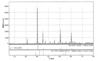
- FIG. 2 is an X-ray diffraction pattern of the oxide sintered body of Example 1.
- FIG. 3 is an X-ray diffraction pattern of an oxide sintered body of Example 12.
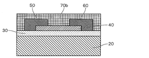
- FIG. It is a figure which shows one Embodiment of TFT of this invention. It is a figure which shows one Embodiment of TFT of this invention.
- the oxide sintered body of the present invention includes a bixbite phase represented by In 2 O 3 and a garnet phase represented by Y 3 In 2 Ga 3 O 12 .
- a sintered compact density (relative density) and reduction of volume resistivity (bulk resistance) are realizable.
- the linear expansion coefficient can be reduced and the thermal conductivity can be increased.
- a sintered body having a low volume resistivity and a high sintered body density is obtained. be able to.
- a high-strength sputtering target (target) can be obtained, microcracks are not generated by thermal stress, chipping and abnormal discharge do not occur, and high power A sputtering target capable of sputtering is obtained.
- the sintered body of the present invention has high target strength.
- the thermal conductivity is high and the linear expansion coefficient is small, thermal stress can be suppressed.
- generation of microcracks and chipping of the target can be suppressed, and generation of nodules and abnormal discharge can be suppressed.
- the sintered body of the present invention has high mobility and heat in a chemical vapor deposition process (CVD process) performed after stacking the oxide semiconductor layer in the TFT manufacturing process or in heat treatment after TFT fabrication. Therefore, a high-performance TFT can be obtained.
- CVD process chemical vapor deposition process
- the bixbite phase represented by In 2 O 3 and the garnet phase represented by Y 3 In 2 Ga 3 O 12 can be detected from the XRD chart by, for example, the X-ray diffraction (XRD) method.
- XRD X-ray diffraction
- the sintered body of the present invention preferably has a bixbite phase represented by In 2 O 3 as a main component.
- the peak intensity ratio (In 2 O 3 / Y 3 In 2 Ga 3 O 12 ) is preferably 1 to 500, more preferably 5 to 300, and even more preferably 7 to 290. By being in the above range, stable sputtering can be performed.
- the peak intensity ratio (In 2 O 3 / Y 3 In 2 Ga 3 O 12 ) can be calculated from, for example, XRD measurement.
- the Vix represented by In 2 O 3 It can be determined by dividing the peak intensity at which the maximum peak of the bite phase appears by the peak intensity at which the maximum peak of the garnet phase represented by Y 3 In 2 Ga 3 O 12 appears.
- Y, Ga, or Y and Ga may be dissolved in the bixbite phase represented by In 2 O 3 . It is preferable that Y and Ga are dissolved in the bixbite phase represented by In 2 O 3 .
- the solid solution is preferably a substitutional solid solution. Thereby, stable sputtering can be performed.
- the solid solution of Y, Ga, or Y and Ga can be identified from the lattice constant of the bixbite phase using, for example, XRD measurement.
- XRD measurement for example, if smaller than the lattice constant of the bixbyite phase only represented by In 2 O 3, the solid solution is superior to the action of Ga If it is larger than the lattice constant of only the bixbite phase represented by In 2 O 3 , the solid solution of Y acts predominantly.
- the “lattice constant” is defined as the length of the lattice axis of the unit cell, and can be obtained by, for example, the X-ray diffraction method.
- Y, In, Ga, or Y, In, and Ga may be dissolved in each site constituting the garnet phase represented by Y 3 In 2 Ga 3 O 12 .
- the solid solution of these metal elements can be confirmed by the fact that the garnet phase contained in the oxide sintered body appears slightly deviated from the composition represented by Y 3 In 2 Ga 3 O 12 . Specifically, it can be confirmed by lead belt analysis. Thereby, stable sputtering can be performed.
- the average particle size of the garnet phase represented by Y 3 In 2 Ga 3 O 12 is preferably 15 ⁇ m or less, more preferably 10 ⁇ m or less, still more preferably 8 ⁇ m or less, and particularly preferably 5 ⁇ m or less. Although there is no restriction
- the average particle diameter of the garnet phase represented by Y 3 In 2 Ga 3 O 12 is, for example, specified by the electron probe microanalyzer (EPMA), and the garnet phase represented by Y 3 In 2 Ga 3 O 12 Assuming a circle whose maximum diameter is the diameter, it can be obtained as an average value of the diameters.
- EPMA electron probe microanalyzer
- the atomic ratio In / (In + Y + Ga) of In element to In element, Y element and Ga element contained in the oxide sintered body is preferably 0.60 or more and 0.97 or less, and 0.70 or more and 0.96. The following is more preferable, and 0.75 or more and 0.95 or less is more preferable.
- In / (In + Y + Ga) is less than 0.60, the movement of the TFT including the oxide semiconductor thin film to be formed may be reduced.
- In / (In + Y + Ga) is more than 0.97, there is a possibility that the stability of the TFT cannot be obtained, or that it becomes difficult to become a semiconductor by conducting.
- the atomic ratio Ga / (In + Y + Ga) of Ga element to In element, Y element and Ga element contained in the oxide sintered body is preferably 0.01 or more and 0.20 or less, and 0.02 or more and 0.15. The following is more preferable, and 0.02 or more and 0.12 or less is more preferable.
- Ga / (In + Y + Ga) is less than 0.01, the garnet phase represented by Y 3 In 2 Ga 3 O 12 is not formed, and the bulk resistance of the sintered body is increased, or the sintered body density and sintering are increased. Since the body strength is low, there is a possibility that cracking due to heat during sputtering is likely to occur, or that stable sputtering cannot be performed.
- Ga / (In + Y + Ga) exceeds 0.20, there is a possibility that the movement of the TFT including the oxide semiconductor thin film to be formed becomes small.
- the atomic ratio Y / (In + Y + Ga) of Y element to In element, Y element, and Ga element contained in the oxide sintered body is preferably 0.02 or more and 0.20 or less, and 0.02 or more and 0.0. 18 or less is more preferable, and 0.03 or more and 0.16 or less is more preferable.
- Y / (In + Y + Ga) is less than 0.02
- the garnet phase represented by Y 3 In 2 Ga 3 O 12 is not formed, the bulk resistance of the sintered body increases, the sintered body density and the sintered body Since the body strength is low, there is a possibility that cracking due to heat during sputtering is likely to occur, or that stable sputtering cannot be performed.
- Y / (In + Y + Ga) exceeds 0.20, the movement of the TFT including the oxide semiconductor thin film to be formed may be reduced.
- the oxide sintered body of the present invention preferably further contains a positive tetravalent metal element. Thereby, sputtering can be performed more stably.
- Examples of the positive tetravalent metal element include Sn, Ti, Zr, Hf, Ce, and Ge. Of the positive tetravalent metal elements, Sn is preferable. Bulk resistance decreases due to the Sn doping effect, and sputtering can be performed more stably.
- the positive tetravalent metal element is preferably dissolved in a bixbite phase represented by In 2 O 3 or a garnet phase represented by Y 3 In 2 Ga 3 O 12 , and is represented by In 2 O 3. More preferably, it is dissolved in the bixbite phase.
- the solid solution is preferably a substitutional solid solution. Thereby, sputtering can be performed more stably.
- the solid solution of the positive tetravalent metal element can be identified from the bulk resistance of the oxide sintered body, for example.
- the bulk resistance of the oxide sintered body when the positive tetravalent metal element is not added or not dissolved is high, and may cause abnormal discharge.
- a positive tetravalent metal element is added and dissolved, the bulk resistance of the oxide sintered body is reduced, and a stable sputtering state can be obtained.
- the content of the positive tetravalent metal element is preferably 100 to 10,000 ppm in terms of atomic concentration with respect to all metal elements in the oxide sintered body, more preferably 500 ppm to 8000 ppm, and still more preferably 800 ppm to 6000 ppm. It is. When the content of the positive tetravalent metal element is less than 100 ppm, the bulk resistance may not be reduced. On the other hand, when the content of the positive tetravalent metal element is more than 10,000 ppm, the oxide semiconductor thin film to be formed may be in a high carrier state and the TFT may be conducted or the on / off value may be reduced.
- the oxide sintered body of the present invention preferably has a relative density of 95% or more, more preferably 96% or more, still more preferably 97% or more, and particularly preferably 98% or more.
- the upper limit is not particularly limited, but is usually 100%.
- the relative density can be calculated, for example, by dividing the measured density of the oxide sintered body measured by the Archimedes method by the theoretical density of the oxide sintered body as a percentage.
- oxide A, oxide B, oxide C, and oxide D are used as the raw material powder of the oxide sintered body
- amount of oxide A, oxide B, oxide C, and oxide D used Assuming that (charge amount) is a (g), b (g), c (g), and d (g), the theoretical density can be calculated by applying as follows.
- Theoretical density (a + b + c + d) / ((a / density of oxide A) + (b / density of oxide B) + (c / density of oxide C) + (d / density of oxide D))
- the value of the specific gravity of the oxide described in the Chemistry Handbook Fundamentals I Nihon Kagaku Revised 2nd edition (Maruzen Co., Ltd.) is used. Good.
- the theoretical density can also be calculated as follows using the weight ratio of each oxide.
- Theoretical density 1 / ((weight ratio of oxide A / density of oxide A) + (weight ratio of oxide B / density of oxide B) + (weight ratio of oxide C / density of oxide C) + (Weight ratio of oxide D / density of oxide D))
- the oxide sintered body of the present invention has a bulk resistance of preferably 30 m ⁇ ⁇ cm or less, more preferably 15 m ⁇ ⁇ cm or less, and further preferably 10 m ⁇ ⁇ cm or less.
- the lower limit is not particularly limited, but is usually 1 m ⁇ ⁇ cm or more.
- the bulk resistance of the oxide sintered body is 30 m ⁇ ⁇ cm or less, abnormal discharge due to charging of the target is less likely to occur during film formation with high power, and the plasma state is stabilized and spark is less likely to occur. Further, when a pulse DC sputtering apparatus is used, the plasma is further stabilized, and it becomes possible to perform sputtering stably without problems such as abnormal discharge.
- the bulk resistance can be measured based on, for example, a four-probe method.
- the oxide sintered body of the present invention preferably has a three-point bending strength of 120 MPa or more, more preferably 140 MPa or more, and further preferably 150 MPa or more.
- the target strength is weak when the sputter film is formed with high power, the target is cracked or chipped, and the chipped fragments are scattered on the target. However, it may cause abnormal discharge.
- the three-point bending strength can be tested in accordance with, for example, JIS R 1601 “Room temperature bending strength test of fine ceramics”. Specifically, using a standard test piece having a width of 4 mm, a thickness of 3 mm, and a length of 40 mm, the test piece is placed on two fulcrums arranged at a fixed distance (30 mm), and the crosshead speed is 0 from the center between the fulcrums. The bending strength can be calculated from the maximum load at the time of breaking by applying a load of 0.5 mm / min.
- the oxide sintered body of the present invention preferably has a linear expansion coefficient of 9.0 ⁇ 10 ⁇ 6 K ⁇ 1 or less, more preferably 8.5 ⁇ 10 ⁇ 6 K ⁇ 1 or less, and 8.0 ⁇ More preferably, it is 10 ⁇ 6 K ⁇ 1 or less.
- the lower limit is not particularly limited, but is usually 5.0 ⁇ 10 ⁇ 6 K ⁇ 1 or more.
- the linear expansion coefficient is, for example, a standard test piece having a width of 5 mm, a thickness of 5 mm, and a length of 10 mm.
- the temperature increase rate is set to 5 ° C./min. It can be obtained by detecting with a detector.
- the oxide sintered body of the present invention preferably has a thermal conductivity of 5.0 W / m ⁇ K or more, more preferably 5.5 W / m ⁇ K or more, and further 6.0 W / m ⁇ K or more. Preferably, 6.5 W / m ⁇ K or more is most preferable.
- the upper limit is not particularly limited, but is usually 10 W / m ⁇ K or less.
- the thermal conductivity can be calculated by, for example, obtaining a specific heat capacity and a thermal diffusivity by a laser flash method using a standard test piece having a diameter of 10 mm and a thickness of 1 mm, and multiplying this by the density of the test piece.
- the oxide sintered body of the present invention preferably has a Young's modulus of 200 GPa or less, more preferably 190 GPa or less, further preferably 185 GPa or less, and most preferably 180 GPa or less.
- the lower limit of the Young's modulus is not particularly limited, but is usually 100 GPa or more. If the Young's modulus of the oxide sintered body is 200 GPa or less, it is preferable that the thermal stress generated during sputtering does not crack.
- the Young's modulus can be obtained by, for example, sound speed measurement by an ultrasonic pulse reflection method.
- the oxide sintered body of the present invention is essentially composed of In, Y, Ga, and optionally a positive tetravalent metal element, and may contain other inevitable impurities as long as the effects of the present invention are not impaired. .
- 90 atomic% or more, 95 atomic% or more, 98 atomic% or more, 99 atomic% or more, or 100 atomic% of the metal element of the oxide sintered body of the present invention is In, Y and Ga, or In, Y , Ga and a positive tetravalent metal element.
- the oxide sintered body of the present invention may include a bixbite phase represented by In 2 O 3 and a garnet phase represented by Y 3 In 2 Ga 3 O 12 as crystal phases, and from only these crystal phases. It may be.
- the oxide sintered body of the present invention is a step of preparing a mixed powder of a raw material powder containing In element, a raw material powder containing Y element, and a raw material powder containing Ga element, and molding the mixed powder to produce a molded body. It can manufacture by the process and the process of baking a molded object.
- the mixed powder may include a raw material powder containing a positive tetravalent metal element.
- the raw material powder is preferably an oxide powder. That is, the raw material powder containing In element is preferably indium oxide powder, the raw material powder containing Y element is preferably yttrium oxide powder, and the raw material powder containing Ga element is preferably gallium oxide powder.
- the raw material powder containing a positive tetravalent metal element is preferably an oxide powder of a positive tetravalent metal element, and more preferably a tin oxide powder.
- the mixing ratio of the raw material powder corresponds to, for example, the atomic ratio of the sintered body to be obtained.
- the average particle diameter of the raw material powder is preferably 0.1 to 1.2 ⁇ m, more preferably 0.5 to 1.0 ⁇ m or less.
- the average particle diameter of the raw material powder can be measured with a laser diffraction type particle size distribution apparatus or the like.
- the method for mixing and forming the raw materials is not particularly limited, and can be performed using a known method.
- a binder may be added when mixing.
- the mixing of the raw materials can be performed using a known device such as a ball mill, a bead mill, a jet mill, or an ultrasonic device.
- the pulverization time may be appropriately adjusted, but is preferably about 6 to 100 hours.
- the molding method may be, for example, pressing a mixed powder into a molded body. By this process, it can be formed into a product shape (for example, a shape suitable as a sputtering target).
- the molding material can be obtained by filling the raw material into a mold and molding it by a die press or cold isostatic press (CIP), for example, at a pressure of 1000 kg / cm 2 or more.
- CIP cold isostatic press
- molding aids such as polyvinyl alcohol, polyethylene glycol, methylcellulose, polywax, oleic acid, and stearic acid may be used.
- the obtained molded body can be sintered at a sintering temperature of 1200 to 1650 ° C. for 10 hours or more, for example, to obtain a sintered body.
- the sintering temperature is preferably 1350 to 1600 ° C, more preferably 1400 to 1600 ° C, still more preferably 1450 to 1600 ° C.
- the sintering time is preferably 10 to 50 hours, more preferably 12 to 40 hours, still more preferably 13 to 30 hours.
- the sintering temperature is less than 1200 ° C. or the sintering time is less than 10 hours, the sintering does not proceed sufficiently, and the electrical resistance of the target is not sufficiently lowered, which may cause abnormal discharge.
- the sintering temperature exceeds 1650 ° C. or the sintering time exceeds 50 hours, the average crystal grain size increases due to remarkable crystal grain growth and the generation of coarse vacancies has occurred. May cause a drop or abnormal discharge.
- the compact is usually sintered in an air atmosphere or an oxygen gas atmosphere.
- the oxygen gas atmosphere is preferably an atmosphere having an oxygen concentration of, for example, 10 to 50% by volume. Even if the temperature raising process is performed in an air atmosphere, the density of the sintered body can be increased.
- the heating rate during sintering is from 50 ° C. to 150 ° C./hour from 800 ° C. to the sintering temperature (1200 to 1650 ° C.).
- the temperature range above 800 ° C. is the range where the sintering proceeds most.
- the rate of temperature rise in this temperature range is slower than 50 ° C./hour, crystal grain growth becomes significant, and there is a possibility that densification cannot be achieved.
- the rate of temperature increase is higher than 150 ° C./hour, a temperature distribution is generated in the molded body, and the sintered body may be warped or cracked.
- the rate of temperature increase from 800 ° C. to the sintering temperature is preferably 60 to 140 ° C./hour, more preferably 70 to 130 ° C./hour.
- the sputtering target of the present invention can be produced using the oxide sintered body described above. Thereby, an oxide semiconductor thin film can be manufactured by vacuum processes, such as sputtering method.
- a sputtering target can be produced by cutting or polishing a sintered body and bonding the sintered body to a backing plate. For example, by cutting, it is possible to remove a highly oxidized sintered portion or an uneven surface on the surface of the sintered body. Also, it can be specified size. The surface may be polished with # 200, # 400, or # 800. Thereby, abnormal discharge and generation of particles during sputtering can be suppressed.
- a bonding method for example, bonding with metal indium can be mentioned.
- the sputtering target of the present invention can be applied to a direct current (DC) sputtering method, a radio frequency (RF) sputtering method, an alternating current (AC) sputtering method, a pulsed DC sputtering method, and the like.
- DC direct current
- RF radio frequency
- AC alternating current
- DC pulsed DC
- An oxide semiconductor thin film can be obtained by forming a film using the above sputtering target. Thereby, a thin film that exhibits excellent TFT performance when used in a TFT can be formed.
- Film formation can be performed by vapor deposition, sputtering, ion plating, pulse laser vapor deposition, or the like.
- the TFT of the present invention includes the above-described oxide semiconductor thin film.
- the oxide semiconductor thin film can be suitably used as a channel layer, for example.
- the element configuration of the TFT is not particularly limited, and various known element configurations can be employed.
- the TFT of the present invention can be used for display devices such as a liquid crystal display and an organic electroluminescence display.
- FIG. 3 shows an example of the TFT of the present invention.
- a semiconductor film 40 obtained by using the sputtering target of the present invention is formed on a gate insulating film 30 on a silicon wafer (gate electrode) 20, and interlayer insulating films 70 and 70a are formed.
- 70a on the semiconductor film 40 also functions as a channel layer protective layer.
- a source electrode 50 and a drain electrode 60 are provided on the semiconductor film.
- FIG. 4 shows an example of the TFT of the present invention.
- a semiconductor film 40 obtained by using the sputtering target of the present invention is formed on a gate insulating film (for example, SiO 2 ) 30 on a silicon wafer (gate electrode) 20, and a source electrode 50 is formed on the semiconductor film 40.
- a drain electrode 60, and a protective layer 70 b is provided on the semiconductor film 40, the source electrode 50, and the drain electrode 60.
- the silicon wafer 20 and the gate insulating film 30 may be a silicon wafer with a thermal oxide film, the silicon wafer may be used as a gate electrode, and the thermal oxide film (SiO 2 ) may be used as a gate insulating film.
- the gate electrode 20 may be formed on a substrate such as glass.
- the semiconductor film preferably has a band gap of 3.0 eV or more.
- the band gap is 3.0 eV or more, light on the long wavelength side from a wavelength near 420 nm is not absorbed.
- light from the light source of the organic EL or TFT-LCD is not absorbed, and when used as a TFT channel layer, there is no malfunction due to the light of the TFT, and light stability can be improved.
- it can.
- it is 3.1 eV or more, More preferably, it is 3.3 eV or more.
- the material for forming each of the drain electrode, the source electrode and the gate electrode is not particularly limited, and a commonly used material can be arbitrarily selected.
- transparent electrodes such as indium tin oxide (ITO), indium zinc oxide (IZO), ZnO, SnO 2 , metal electrodes such as Al, Ag, Cu, Cr, Ni, Mo, Au, Ti, Ta, or these
- metal electrode or a laminated electrode of an alloy containing can be used.
- a silicon wafer may be used as a substrate, and in that case, the silicon wafer also acts as an electrode.
- a protective film on the drain electrode, the source electrode, and the channel layer.
- the durability is easily improved even when the TFT is driven for a long time.
- a top gate type TFT has a structure in which a gate insulating film is formed on a channel layer, for example.
- the protective film or the insulating film can be formed by, for example, CVD, but at that time, the process may be performed at a high temperature.
- the protective film or the insulating film often contains an impurity gas immediately after film formation, and it is preferable to perform heat treatment (annealing treatment).
- the oxide semiconductor thin film of the present invention By removing these impurity gases by heat treatment, a stable protective film or insulating film is obtained, and a highly durable TFT element can be easily formed.
- the oxide semiconductor thin film of the present invention it becomes difficult to be affected by the temperature in the CVD process and the subsequent heat treatment, so that the TFT characteristics can be stabilized even when a protective film or an insulating film is formed. Can be improved.
- Examples 1-14 Manufacture of oxide sintered bodies
- Indium oxide powder, gallium oxide powder, yttrium oxide powder and tin oxide powder are weighed so as to have the atomic ratio and Sn atomic concentration of the oxide sintered bodies shown in Tables 1 and 2, and placed in a polyethylene pot.
- the mixture was pulverized for 72 hours using a dry ball mill to produce a mixed powder.
- This mixed powder was put into a mold and formed into a press-molded body at a pressure of 500 kg / cm 2 .
- This molded body was densified by CIP at a pressure of 2000 kg / cm 2 .
- this molded body was placed in a normal pressure firing furnace, held at 350 ° C. for 3 hours in an air atmosphere, then heated at 100 ° C./hour, sintered at 1450 ° C. for 20 hours, Then, it was left to cool and an oxide sintered body (sintered body) was obtained.
- FIG. 1 An XRD chart of the obtained sintered body in Example 1 is shown in FIG. In FIG. 1, a portion having an intensity of 5500 or more is omitted. From FIG. 1, it was found that the sintered body of Example 1 had “a bixbite phase represented by In 2 O 3 ” and “a garnet phase represented by Y 3 In 2 Ga 3 O 12 ”. Further, for Example 12, an XRD chart of the obtained sintered body is shown in FIG. In FIG. 2, a portion having an intensity of 10500 or more is omitted. From FIG. 2, it was found that the sintered body of Example 12 had “a bixbite phase represented by In 2 O 3 ” and “a garnet phase represented by Y 3 In 2 Ga 3 O 12 ”.
- the maximum peak intensity of the bixbite phase represented by In 2 O 3 and the maximum of the garnet phase represented by Y 3 In 2 Ga 3 O 12 The peak intensity ratio (In 2 O 3 / Y 3 In 2 Ga 3 O 12 ) with respect to the peak intensity was similarly determined. The results are shown in Tables 1 and 2.
- the sintered bodies of Examples 2 to 11 and 13 to 14 were obtained from the XRD chart according to “Bixbite phase represented by In 2 O 3 ” and “Garnet phase represented by Y 3 In 2 Ga 3 O 12. ".
- the lattice constant of the bixbyite structure of “the bixbyite phase represented by In 2 O 3 ” was obtained.
- the results are shown in Tables 1 and 2. From the obtained lattice constant, it can be seen that the sintered bodies of Examples 1 and 2 have Y and Ga dissolved in the bixbite phase represented by In 2 O 3 , and the sintered body of Example 1 is It turned out that the solid solution of Y acts preferentially, and the solid solution of Ga acts preferentially in the sintered body of Example 2. In the sintered bodies of Examples 3 to 14, it was found from the lattice constants obtained that Y, Ga and Sn were dissolved in the bixbite phase represented by In 2 O 3 .
- the bulk resistance (conductivity) of the above-mentioned sintered body was measured based on the four-probe method (JISR1637) using a resistivity meter Loresta (Mitsubishi Chemical Corporation, Loresta AX MCP-T370). The results are shown in Tables 1 and 2.
- the firing method in an atmospheric atmosphere using an atmospheric firing furnace is a sintered body rather than a technique using HIP (Hot Isostatic Press), discharge plasma sintering (SPS), or an atmospheric firing furnace.
- HIP Hot Isostatic Press
- SPS discharge plasma sintering
- an atmospheric firing furnace high-density sintered bodies of Examples 1 to 14 were obtained by firing in an air atmosphere using a simple atmospheric pressure firing furnace.
- the linear expansion coefficient was obtained by cutting the obtained sintered body into a width of 5 mm, a thickness of 5 mm, and a length of 10 mm as a standard test piece, setting the heating rate to 10 ° C./min, and 30 to 300 ° C.
- the average thermal expansion coefficient at 0 ° C. was measured by a thermomechanical analysis method from a thermomechanical analyzer TMA7100 (Hitachi High-Tech Science Co., Ltd.).
- the thermal conductivity was determined by measuring the specific heat capacity with a thermal constant measuring device (TC-9000 specially manufactured by ULVAC-RIKO) using a laser flash method using the obtained sintered body cut to a diameter of 10 mm and a thickness of 2 mm as a standard test piece.
- Type and thermal diffusivity were calculated using a thermophysical property measuring apparatus (LFA501 manufactured by Kyoto Electronics Industry Co., Ltd.), and this was calculated by multiplying this by the outer dimensions of the test piece and the density determined from the weight measurement.
- the Young's modulus is obtained by cutting the obtained sintered body into a diameter of 20 mm and a thickness of 5 mm as a standard test piece, and using an ultrasonic flaw detector (Panametrics, 5900PR) at room temperature, in the atmosphere, in the thickness direction. Obtained by measurement.
- Example 2 An oxide sintered body (sintered body) was obtained.
- the crystal structure of the obtained sintered body was only a bixbite structure represented by In 2 O 3 .
- the lattice constant ( ⁇ ) of the bixbite structure was 10.0686 ⁇
- the relative density (%) was 96.0%
- the bulk resistance was 3.6 m ⁇ cm.
- the obtained oxide sintered body was evaluated for the linear expansion coefficient and the thermal conductivity in the same manner as in Example 2. Table 3 shows the results of the measured linear expansion coefficient and thermal conductivity.
- Sputtering targets were prepared for the sintered bodies of Examples 1 to 14.
- Example 15 Using the sputtering target of Example 5 obtained, an oxide semiconductor layer (channel layer) was formed by sputtering on a silicon substrate with a thermal oxide film using a channel-shaped metal mask.
- a gold electrode was formed to a thickness of 50 nm using a source / drain shaped metal mask.
- annealing was performed in air at 300 ° C. for 1 hour to obtain a simple TFT having a bottom gate and top contact with a channel length of 200 ⁇ m and a channel width of 1000 ⁇ m.
- the oxide sintered body of the present invention can be used for a sputtering target, and the sputtering target of the present invention can be used for manufacturing an oxide semiconductor thin film and a thin film transistor.
Landscapes
- Chemical & Material Sciences (AREA)
- Engineering & Computer Science (AREA)
- Materials Engineering (AREA)
- Organic Chemistry (AREA)
- Ceramic Engineering (AREA)
- Chemical Kinetics & Catalysis (AREA)
- Mechanical Engineering (AREA)
- Metallurgy (AREA)
- Manufacturing & Machinery (AREA)
- Structural Engineering (AREA)
- Inorganic Chemistry (AREA)
- Physics & Mathematics (AREA)
- Plasma & Fusion (AREA)
- Analytical Chemistry (AREA)
- Physical Vapour Deposition (AREA)
- Thin Film Transistor (AREA)
- Conductive Materials (AREA)
- Manufacturing Of Electric Cables (AREA)
- Physical Deposition Of Substances That Are Components Of Semiconductor Devices (AREA)
- Compositions Of Oxide Ceramics (AREA)
Abstract
Description
1.In2O3で表されるビックスバイト相、及び
Y3In2Ga3O12で表されるガーネット相を含む酸化物焼結体。
2.In、Ga及びYの原子比が、下記の範囲である1に記載の酸化物焼結体。
In/(In+Y+Ga)が0.60以上0.97以下
Ga/(In+Y+Ga)が0.01以上0.20以下
Y/(In+Y+Ga)が0.02以上0.20以下
3.前記In2O3で表されるビックスバイト相の最大ピーク強度の、前記Y3In2Ga3O12で表されるガーネット相の最大ピーク強度に対する、ピーク強度比が、1~500である1又は2に記載の酸化物焼結体。
4.さらに、正四価の金属元素を含む1~3のいずれかに記載の酸化物焼結体。
5.前記正四価の金属元素が、前記In2O3で表されるビックスバイト相又はY3In2Ga3O12で表されるガーネット相に固溶している4に記載の酸化物焼結体。
6.前記正四価の金属元素の含有量が、酸化物焼結体中の全金属元素に対して、原子濃度で100~10000ppmである、4又は5に記載の酸化物焼結体。
7.前記正四価の金属元素がSnである4~6のいずれかに記載の酸化物焼結体。
8.相対密度が95%以上である1~7のいずれかに記載の酸化物焼結体。
9.バルク抵抗が、30mΩ・cm以下である1~8のいずれかに記載の酸化物焼結体。
10.1~9のいずれかに記載の酸化物焼結体を含むスパッタリングターゲット。
11.10に記載のスパッタリングターゲットを用いる酸化物半導体薄膜の製造方法。
12.11に記載の酸化物半導体薄膜を含む薄膜トランジスタの製造方法。
本発明の焼結体(酸化物焼結体)により、強度が高いスパッタリングターゲット(ターゲット)を得ることができ、熱応力によりマイクロクラックを発生せず、チッピングや異常放電をおこさず、大パワーでのスパッタリングが可能なスパッタリングターゲットを得ることができる。
本発明の焼結体は、ターゲットの強度が高い。また熱伝導率が高く、線膨張係数が小さいため、熱応力を抑えることができ、その結果、ターゲットのマイクロクラックやチッピングの発生を抑制し、ノジュールや異常放電の発生を抑制することができる。
加えて、本発明の焼結体により、高移動度で、TFT製造プロセス過程で酸化物半導体層の積層後に行われる化学気相成長プロセス(CVDプロセス)やTFT作製後の加熱処理等での熱による特性への劣化が少なく、高性能のTFTを得ることができる。
上記範囲内であることにより、安定したスパッタを行うことができる。
具体的には、In2O3で表されるビックスバイト相の最大ピークが現れるピーク強度(2θ/θ=30~31°付近、例えば、29.5~31°)と、Y3In2Ga3O12で表されるガーネット相の最大ピークが現れるピーク強度(2θ/θ=32°付近、例えば、31.1~32.5°)とを用いて、In2O3で表されるビックスバイト相の最大ピークが現れるピーク強度を、Y3In2Ga3O12で表されるガーネット相の最大ピークが現れるピーク強度で除することで求めることができる。
これにより、安定したスパッタを行うことができる。
In2O3で表されるビックスバイト相の格子定数が、例えば、In2O3で表されるビックスバイト相のみの格子定数よりも小さくなっていれば、Gaの固溶が優位的に作用しており、In2O3で表されるビックスバイト相のみの格子定数よりも大きくなっていれば、Yの固溶が優位的に作用している。
これら金属元素が固溶していることは、酸化物焼結体に含まれるガーネット相が、Y3In2Ga3O12で表される組成から少し外れて現れることにより確認できる。具体的には、リードベルト解析で確認することができる。
これにより、安定したスパッタを行うことができる。
Y3In2Ga3O12で表されるガーネット相の平均粒径が15μm以下の場合、放電を安定化しやすくなる。
Y3In2Ga3O12で表されるガーネット相の平均粒径は、例えば、電子プローブ微小分析器(EPMA)により、Y3In2Ga3O12で表されるガーネット相を特定し、その最大径を直径とする円を仮定し、その直径の平均値として、求めることができる。
In/(In+Y+Ga)が0.60未満の場合、形成する酸化物半導体薄膜を含むTFTの移動動が小さくなるおそれがある。In/(In+Y+Ga)が0.97超の場合、TFTの安定性が得られないおそれや、導電化して半導体になりにくいおそれがある。
Ga/(In+Y+Ga)が0.01未満の場合、Y3In2Ga3O12で表されるガーネット相が形成されず、焼結体のバルク抵抗が高くなったり、焼結体密度及び焼結体強度が低く、そのためスパッタ時の熱による割れ等が発生しやすくなったり、安定したスパッタリングができなくなるおそれがある。一方、Ga/(In+Y+Ga)が0.20超の場合、形成する酸化物半導体薄膜を含むTFTの移動動が小さくなるおそれがある。
Y/(In+Y+Ga)が0.02未満の場合、Y3In2Ga3O12で表されるガーネット相が形成されず、焼結体のバルク抵抗が高くなったり、焼結体密度及び焼結体強度が低く、そのためスパッタ時の熱による割れ等が発生しやすくなったり、安定したスパッタリングができなくなるおそれがある。一方、Y/(In+Y+Ga)が0.20超の場合、形成する酸化物半導体薄膜を含むTFTの移動動が小さくなるおそれがある。
これにより、より安定的にスパッタリングを行うことができる。
上記正四価の金属元素のうちSnが好ましい。Snのドーピング効果によりバルク抵抗が低下し、より安定的にスパッタリングを行うことができる。
これにより、より安定的にスパッタリングを行うことができる。
正四価の金属元素の含有量が100ppm未満の場合、バルク抵抗が低下しないおそれがある。一方、正四価の金属元素の含有量が10000ppm超の場合、形成する酸化物半導体薄膜が高キャリア状態になりTFTが導通するおそれや、オン/オフ値が小さくなるおそれがある。
酸化物焼結体の相対密度が95%以上の場合、ターゲットとして用いた際に、異常放電の原因やノジュール発生の起点となる空隙を減少させることができる。
相対密度は、例えば、アルキメデス法で測定した酸化物焼結体の実測密度を、酸化物焼結体の理論密度で除した値を、百分率にして、算出することができる。
例えば、酸化物焼結体の原料粉末として酸化物A、酸化物B、酸化物C、酸化物Dを用いた場合において、酸化物A、酸化物B、酸化物C、酸化物Dの使用量(仕込量)をそれぞれa(g)、b(g)、c(g)、d(g)とすると、理論密度は、以下のように当てはめることで算出できる。
理論密度=(a+b+c+d)/((a/酸化物Aの密度)+(b/酸化物Bの密度)+(c/酸化物Cの密度)+(d/酸化物Dの密度))
尚、各酸化物の密度は、密度と比重はほぼ同等であることから、化学便覧 基礎編I日本化学編 改定2版(丸善株式会社)に記載されている酸化物の比重の値を用いるとよい。なお、理論密度は、各酸化物の重量比を用いて以下のように算出することもできる。
理論密度=1/((酸化物Aの重量比/酸化物Aの密度)+(酸化物Bの重量比/酸化物Bの密度)+(酸化物Cの重量比/酸化物Cの密度)+(酸化物Dの重量比/酸化物Dの密度))
酸化物焼結体のバルク抵抗が30mΩ・cm以下の場合、大パワーでの成膜時に、ターゲットの帯電による異常放電が発生しにくく、また、プラズマ状態が安定し、スパークが発生しにくくなる。また、パルスDCスパッタ装置を用いる場合、さらにプラズマが安定し、異常放電等の問題もなく、安定してスパッタできるようになる。
バルク抵抗は、例えば、四探針法に基づき測定することができる。
酸化物焼結体の3点曲げ強度が120MPa未満の場合、大パワーでスパッタ成膜した際に、ターゲットの強度が弱く、ターゲットが割れたり、チッピングを起こして、チッピングした破片がターゲット上に飛散し、異常放電の原因となるおそれがある。
具体的には、幅4mm、厚さ3mm、長さ40mmの標準試験片を用いて、一定距離(30mm)に配置された2支点上に試験片を置き、支点間の中央からクロスヘッド速度0.5mm/分荷重を加え、破壊した時の最大荷重より、曲げ強さを算出することができる。
酸化物焼結体の線膨張係数が9.0×10⁻⁶K-1を超える場合、大パワーでスパッタリング中に加熱され、ターゲットが膨張し、ボンディングされている銅版側との間で変形が起こり、応力によりターゲットにマイクロクラックが入ったり、割れやチッピングにより、異常放電の原因となるおそれがある。
線膨張係数は、例えば幅5mm、厚さ5mm、長さ10mmの標準試験片を用いて、昇温速度を5℃/分にセットし、300℃に到達した時の熱膨張による変位を、位置検出機で検出することにより求めることができる。
上限値は、特に制限はないが、通常10W/m・K以下である。
酸化物焼結体の熱伝導率が5.0W/m・K未満の場合、大パワーでスパッタリング成膜した際に、スパッタ面とボンディングされた面の温度が異なり、内部応力によりターゲットにマイクロクラックや割れ、チッピングが発生するおそれがある。
熱伝導率は、例えば直径10mm、厚さ1mmの標準試験片を用いて、レーザーフラッシュ法により比熱容量と熱拡散率を求め、これに試験片の密度を乗算することにより算出できる。
ヤング率の下限値は、特に制限はないが、通常100GPa以上である。
酸化物焼結体のヤング率が200GPa以下であれば、スパッタリング中に発生する熱応力でも割れなくなり好ましい。
ヤング率は、例えば超音波パルス反射法による音速測定より求めることができる。
本発明の酸化物焼結体の金属元素の、例えば、90原子%以上、95原子%以上、98原子%以上、99原子%以上又は100原子%が、In、Y及びGa、又はIn、Y、Ga及び正四価の金属元素からなっていてもよい。
混合粉末は、正四価の金属元素を含む原料粉末を含んでもよい。
原料粉末は、酸化物粉末が好ましい。即ち、In元素を含む原料粉末は、酸化インジウム粉末が好ましく、Y元素を含む原料粉末は、酸化イットリウム粉末が好ましく、Ga元素を含む原料粉末は、酸化ガリウム粉末が好ましい。正四価の金属元素を含む原料粉末は、正四価の金属元素の酸化物粉末が好ましく、なかでも酸化スズ粉末が好ましい。
原料の混合は、例えば、ボールミル、ビーズミル、ジェットミル又は超音波装置等の公知の装置を用いて行うことができる。粉砕時間は、適宜調整すればよいが、6~100時間程度が好ましい。
尚、成形処理に際しては、ポリビニルアルコールやポリエチレングリコール、メチルセルロース、ポリワックス、オレイン酸、ステアリン酸等の成形助剤を用いてもよい。
焼結温度は、好ましくは1350~1600℃、より好ましくは1400~1600℃、さらに好ましくは1450~1600℃である。焼結時間は好ましくは10~50時間、より好ましくは12~40時間、さらに好ましくは13~30時間である。
本発明の酸化物焼結体において800℃から上の温度範囲は、焼結が最も進行する範囲である。この温度範囲での昇温速度が50℃/時間より遅くなると、結晶粒成長が著しくなって、高密度化を達成することができないおそれがある。一方、昇温速度が150℃/時間より速くなると、成形体に温度分布が生じ、焼結体が反ったり割れたりするおそれがある。
800℃から焼結温度における昇温速度は、好ましくは60~140℃/時間、より好ましくは70~130℃/時間である。
例えば、切断加工することで、焼結体表面の、高酸化状態の焼結部や、凸凹した面を除くことができる。また、指定の大きさにすることができる。
表面を#200番、もしくは#400番、さらには#800番の研磨を行ってもよい。これにより、スパッタリング中の異常放電やパーティクルの発生を抑えることができる。
ボンディングの方法としては、例えば金属インジウムにより接合することが挙げられる。
TFTの素子構成は特に限定されず、公知の各種の素子構成を採用することができる。本発明TFTは、例えば液晶ディスプレイや有機エレクトロルミネッセンスディスプレイ等の表示装置等に用いることができる。
シリコンウエハー20及びゲート絶縁膜30は、熱酸化膜付きシリコンウエハーを用いて、シリコンウエハーをゲート電極とし、熱酸化膜(SiO2)をゲート絶縁膜としてもよい。
保護膜又は絶縁膜は、例えばCVDにより形成することができるが、その際に高温度によるプロセスになる場合がある。また、保護膜又は絶縁膜は、成膜直後は不純物ガスを含有していることが多く、加熱処理(アニール処理)を行うことが好ましい。加熱処理によりそれらの不純物ガスを取り除くことにより安定した保護膜又は絶縁膜となり、耐久性の高いTFT素子を形成しやすくなる。
本発明の酸化物半導体薄膜を用いることにより、CVDプロセスにおける温度の影響、及びその後の加熱処理による影響を受けにくくなるため、保護膜又は絶縁膜を形成した場合であっても、TFT特性の安定性を向上させることができる。
(酸化物焼結体の製造)
酸化インジウム粉末、酸化ガリウム粉末、酸化イットリウム粉末及び酸化スズ粉末を、表1及び2に示す酸化物焼結体の原子比及びSn原子濃度となるように、秤量し、ポリエチレン製のポットに入れて、乾式ボールミルにより72時間混合粉砕し、混合粉末を作製した。
この混合粉末を金型に入れ、500kg/cm2の圧力でプレス成型体とした。この成型体を2000kg/cm2の圧力でCIPにより緻密化を行った。次に、この成型体を常圧焼成炉に設置して、大気雰囲気下で、350℃で3時間保持した後に、100℃/時間にて昇温し、1450℃にて20時間焼結し、その後、放置して冷却し、酸化物焼結体(焼結体)を得た。
得られた焼結体について、X線回折測定装置Smartlabにより、以下の条件で、焼結体のX線回折(XRD)を測定した。得られたXRDチャートをJADE6により分析し、焼結体中の結晶相を求めた。結果を表1及び2に示す。表1及び2中、「In2O3」は「In2O3で表されるビックスバイト相」を示し、「Y3In2Ga3O12」は「Y3In2Ga3O12で表されるガーネット相」を示す。
・X線:Cu-Kα線(波長1.5418Å、グラファイトモノクロメータにて単色化)
・2θ-θ反射法、連続スキャン(2.0°/分)
・サンプリング間隔:0.02°
・スリットDS(発散スリット)、SS(散乱スリット)、RS(受光スリット):1.0mm
図1から、実施例1の焼結体は、「In2O3で表されるビックスバイト相」及び「Y3In2Ga3O12で表されるガーネット相」を有することが分かった。
また、実施例12について、得られた焼結体のXRDチャートを図2に示す。図2中、強度10500以上の部分は省略した。図2から、実施例12の焼結体は、「In2O3で表されるビックスバイト相」及び「Y3In2Ga3O12で表されるガーネット相」を有することが分かった。
In2O3で表されるビックスバイト相の最大ピーク強度の、Y3In2Ga3O12で表されるガーネット相の最大ピーク強度に対する、ピーク強度比(In2O3/Y3In2Ga3O12)は、In2O3で表されるビックスバイト相の最大ピーク強度が現れる2θ/θ=30~31°付近のピーク強度を、Y3In2Ga3O12で表されるガーネット相の最大ピーク強度が現れる2θ/θ=32°付近のピーク強度で除することで求めた。
実施例1の焼結体において、In2O3で表されるビックスバイト相の最大ピーク強度の、Y3In2Ga3O12で表されるガーネット相の最大ピーク強度に対する、ピーク強度比(In2O3/Y3In2Ga3O12)は71.09であった。
また、実施例2~11及び13~14の焼結体は、XRDチャートから、「In2O3で表されるビックスバイト相」及び「Y3In2Ga3O12で表されるガーネット相」を有することが分かった。
得られた格子定数から、実施例1及び2の焼結体はIn2O3で表されるビックスバイト相にY及びGaが固溶していることが分かり、実施例1の焼結体はYの固溶が優位的に作用しており、実施例2の焼結体はGaの固溶が優位的に作用していることが分かった。
また、実施例3~14の焼結体においては、得られた格子定数からIn2O3で表されるビックスバイト相にY、Ga及びSnが固溶していることが分かった。
上述の焼結体について、電子プローブ微小分析器(EPMA)により、焼結体中のY3In2Ga3O12で表されるガーネット相を50μm×50μmの視野の中で特定し、ガーネット相の最大径を直径とする円(外接円)を仮定し、焼結体に含まれる複数のガーネット相の直径の平均値を、ガーネット相の平均粒径とした。結果を表1及び2に示す。
上述の焼結体について、アルキメデス法で測定した実測密度を、各構成元素の酸化物の密度及び重量比から算出される理論密度で除した値を、百分率にして、算出した。結果を表1及び2に示す。
尚、各原料粉末の密度は、密度と比重はほぼ同等であることから、化学便覧 基礎編I日本化学編 改定2版(丸善株式会社)に記載されている酸化物の比重の値を用いた。
上述の焼結体のバルク抵抗(導電性)を、抵抗率計ロレスタ(三菱化学株式会社製、ロレスタAX MCP-T370)を使用して、四探針法(JISR1637)に基づき測定した。結果を表1及び2に示す。


実施例2及び実施例11で製造した焼結体について、線膨張係数、熱伝導率及びヤング率をそれぞれ測定した。結果を表3に示す。
線膨張係数は、得られた焼結体を幅5mm、厚さ5mm、長さ10mmに切り出したものを標準試験片として用いて、昇温速度を10℃/分にセットし、30℃~300℃の平均熱膨張率を熱機械分析法により、熱機械分析装置TMA7100((株)日立ハイテクサイエンス )より計測した。
熱伝導率は、得られた焼結体を直径10mm、厚さ2mmに切り出したものを標準試験片として用いて、レーザーフラッシュ法により、比熱容量を熱定数測定装置(アルバック理工製 TC-9000特型)及び熱拡散率を熱物性測定装置(京都電子工業製 LFA501)を用いて求め、これに試験片の外形寸法、重量測定より求めた密度を乗算することにより算出した。
ヤング率は、得られた焼結体を直径20mm、厚さ5mmに切り出したものを標準試験片として用いて、超音波探傷装置(Panametrics社製、5900PR)で室温、大気中、板厚方向の測定で求めた。
酸化インジウム粉末、酸化ガリウム粉末を、それぞれ、95:5wt%(In/(In+Ga)=0.928、Ga/(On+Ga)=0.072)なるように、秤量し、ポリエチレン製のポットに入れて、乾式ボールミルにより72時間混合粉砕し、混合粉末を作製した。
この混合粉末を金型に入れ、500kg/cm2の圧力でプレス成型体とした。この成型体を2000kg/cm2の圧力でCIPにより緻密化を行った。次に、この成型体を常圧焼成炉に設置して、大気雰囲気下で、350℃で3時間保持した後に、100℃/時間にて昇温し、1430℃にて28時間焼結し、その後、放置して冷却し、酸化物焼結体(焼結体)を得た。
得られた酸化物焼結体について、実施例1と同様の評価を行った。その結果、得られた焼結体の結晶構造はIn2O3で表されるビックスバイト構造のみであることを確認した。ビックスバイト構造の格子定数(Å)=10.0686Å、相対密度(%)=96.0%、バルク抵抗=3.6mΩcmであった。
また、得られた酸化物焼結体について、実施例2と同様にして線膨張係数及び熱伝導率を評価した。測定した線膨張係数、熱伝導率の結果を表3に示す。

実施例1~14の焼結体について、スパッタリングターゲットを作製した。
得られた実施例5のスパッタリングターゲットを用いて、熱酸化膜付きシリコン基板上にチャネル形状のメタルマスクを用い、酸化物半導体層(チャネル層)をスパッタリングにより成膜した。スパッタリング条件は、スパッタ圧=1Pa,酸素分圧=5%、基板温度=室温で行い、膜厚は50nmに設定した。次に、ソース・ドレイン形状のメタルマスクを用い、金電極を50nm成膜した。最後に、空気中300℃、1時間の条件でアニールすることで、チャネル長200μm、チャネル幅1000μmのボトムゲート、トップコンタクトの簡易型TFTを得た。アニール条件としては、250℃~450℃、0.5時間~10時間の範囲でチャネルドーピングの効果を見ながら適宜選択した。アニール後の薄膜のX線回折結果より、薄膜は結晶化しており、その結晶構造はIn2O3型のビックスバイト構造であった。
得られたTFTの特性を評価した結果、移動度=28cm2/V・sec、電流値が10-8Aを超えるゲート電圧の値Vth>0.51V、S値(Swing Factor)=0.71であった。
本願のパリ優先の基礎となる日本出願明細書の内容を全てここに援用する。
Claims (12)
- In2O3で表されるビックスバイト相、及び
Y3In2Ga3O12で表されるガーネット相を含む酸化物焼結体。 - In、Ga及びYの原子比が、下記の範囲である請求項1に記載の酸化物焼結体。
In/(In+Y+Ga)が0.60以上0.97以下
Ga/(In+Y+Ga)が0.01以上0.20以下
Y/(In+Y+Ga)が0.02以上0.20以下 - 前記In2O3で表されるビックスバイト相の最大ピーク強度の、前記Y3In2Ga3O12で表されるガーネット相の最大ピーク強度に対する、ピーク強度比が、1~500である請求項1又は2に記載の酸化物焼結体。
- さらに、正四価の金属元素を含む請求項1~3のいずれかに記載の酸化物焼結体。
- 前記正四価の金属元素が、前記In2O3で表されるビックスバイト相又はY3In2Ga3O12で表されるガーネット相に固溶している請求項4に記載の酸化物焼結体。
- 前記正四価の金属元素の含有量が、酸化物焼結体中の全金属元素に対して、原子濃度で100~10000ppmである、請求項4又は5に記載の酸化物焼結体。
- 前記正四価の金属元素がSnである請求項4~6のいずれかに記載の酸化物焼結体。
- 相対密度が95%以上である請求項1~7のいずれかに記載の酸化物焼結体。
- バルク抵抗が、30mΩ・cm以下である請求項1~8のいずれかに記載の酸化物焼結体。
- 請求項1~9のいずれかに記載の酸化物焼結体を含むスパッタリングターゲット。
- 請求項10に記載のスパッタリングターゲットを用いる酸化物半導体薄膜の製造方法。
- 請求項11に記載の酸化物半導体薄膜を含む薄膜トランジスタの製造方法。
Priority Applications (4)
| Application Number | Priority Date | Filing Date | Title |
|---|---|---|---|
| CN201780036417.5A CN109311756B (zh) | 2016-06-17 | 2017-06-16 | 氧化物烧结体以及溅射靶 |
| US16/310,388 US11328911B2 (en) | 2016-06-17 | 2017-06-16 | Oxide sintered body and sputtering target |
| KR1020197000886A KR102353398B1 (ko) | 2016-06-17 | 2017-06-16 | 산화물 소결체 및 스퍼터링 타깃 |
| JP2018524029A JP6885940B2 (ja) | 2016-06-17 | 2017-06-16 | 酸化物焼結体及びスパッタリングターゲット |
Applications Claiming Priority (2)
| Application Number | Priority Date | Filing Date | Title |
|---|---|---|---|
| JP2016-121063 | 2016-06-17 | ||
| JP2016121063 | 2016-06-17 |
Publications (1)
| Publication Number | Publication Date |
|---|---|
| WO2017217529A1 true WO2017217529A1 (ja) | 2017-12-21 |
Family
ID=60664172
Family Applications (1)
| Application Number | Title | Priority Date | Filing Date |
|---|---|---|---|
| PCT/JP2017/022276 Ceased WO2017217529A1 (ja) | 2016-06-17 | 2017-06-16 | 酸化物焼結体及びスパッタリングターゲット |
Country Status (6)
| Country | Link |
|---|---|
| US (1) | US11328911B2 (ja) |
| JP (1) | JP6885940B2 (ja) |
| KR (1) | KR102353398B1 (ja) |
| CN (1) | CN109311756B (ja) |
| TW (1) | TWI778964B (ja) |
| WO (1) | WO2017217529A1 (ja) |
Cited By (3)
| Publication number | Priority date | Publication date | Assignee | Title |
|---|---|---|---|---|
| WO2020138319A1 (ja) * | 2018-12-28 | 2020-07-02 | 出光興産株式会社 | 焼結体 |
| WO2023189834A1 (ja) * | 2022-03-29 | 2023-10-05 | 出光興産株式会社 | スパッタリングターゲット、スパッタリングターゲットの製造方法、結晶酸化物薄膜、薄膜トランジスタ、及び電子機器 |
| US20240105819A1 (en) * | 2022-09-27 | 2024-03-28 | Japan Display Inc. | Method for manufacturing semiconductor device |
Families Citing this family (1)
| Publication number | Priority date | Publication date | Assignee | Title |
|---|---|---|---|---|
| CN105873881A (zh) * | 2013-12-27 | 2016-08-17 | 出光兴产株式会社 | 氧化物烧结体、该烧结体的制造方法及溅射靶 |
Citations (4)
| Publication number | Priority date | Publication date | Assignee | Title |
|---|---|---|---|---|
| JPH09209134A (ja) * | 1996-01-31 | 1997-08-12 | Idemitsu Kosan Co Ltd | ターゲットおよびその製造方法 |
| JP2000169219A (ja) * | 1998-12-09 | 2000-06-20 | Jiomatetsuku Kk | 金属酸化物焼結体およびその用途 |
| WO2010032432A1 (ja) * | 2008-09-19 | 2010-03-25 | 出光興産株式会社 | 酸化イットリウムを含有する焼結体及びスパッタリングターゲット |
| WO2015098060A1 (ja) * | 2013-12-27 | 2015-07-02 | 出光興産株式会社 | 酸化物焼結体、その製造方法及びスパッタリングターゲット |
Family Cites Families (6)
| Publication number | Priority date | Publication date | Assignee | Title |
|---|---|---|---|---|
| JPS6272597A (ja) | 1985-09-25 | 1987-04-03 | Shin Etsu Chem Co Ltd | 酸化物ガ−ネツト単結晶 |
| JP2007112951A (ja) | 2005-10-24 | 2007-05-10 | Fujifilm Corp | 無機化合物及びこれを含む組成物と成形体、発光装置、固体レーザ装置 |
| EP2471972B1 (en) | 2006-12-13 | 2014-01-29 | Idemitsu Kosan Co., Ltd. | Sputtering target |
| WO2009005617A1 (en) | 2007-07-03 | 2009-01-08 | The Gates Corporation | Power transmission belt |
| KR20150098060A (ko) | 2014-02-19 | 2015-08-27 | 엘지전자 주식회사 | 영상 표시 기기 및 그의 동작 방법 |
| CN109641757B (zh) * | 2016-08-31 | 2022-02-25 | 出光兴产株式会社 | 石榴石型化合物、含有该化合物的烧结体以及溅射靶 |
-
2017
- 2017-06-16 CN CN201780036417.5A patent/CN109311756B/zh active Active
- 2017-06-16 WO PCT/JP2017/022276 patent/WO2017217529A1/ja not_active Ceased
- 2017-06-16 JP JP2018524029A patent/JP6885940B2/ja active Active
- 2017-06-16 KR KR1020197000886A patent/KR102353398B1/ko active Active
- 2017-06-16 US US16/310,388 patent/US11328911B2/en active Active
- 2017-06-16 TW TW106120191A patent/TWI778964B/zh active
Patent Citations (4)
| Publication number | Priority date | Publication date | Assignee | Title |
|---|---|---|---|---|
| JPH09209134A (ja) * | 1996-01-31 | 1997-08-12 | Idemitsu Kosan Co Ltd | ターゲットおよびその製造方法 |
| JP2000169219A (ja) * | 1998-12-09 | 2000-06-20 | Jiomatetsuku Kk | 金属酸化物焼結体およびその用途 |
| WO2010032432A1 (ja) * | 2008-09-19 | 2010-03-25 | 出光興産株式会社 | 酸化イットリウムを含有する焼結体及びスパッタリングターゲット |
| WO2015098060A1 (ja) * | 2013-12-27 | 2015-07-02 | 出光興産株式会社 | 酸化物焼結体、その製造方法及びスパッタリングターゲット |
Cited By (6)
| Publication number | Priority date | Publication date | Assignee | Title |
|---|---|---|---|---|
| WO2020138319A1 (ja) * | 2018-12-28 | 2020-07-02 | 出光興産株式会社 | 焼結体 |
| JP6788151B1 (ja) * | 2018-12-28 | 2020-11-18 | 出光興産株式会社 | 焼結体 |
| KR20210106462A (ko) * | 2018-12-28 | 2021-08-30 | 이데미쓰 고산 가부시키가이샤 | 소결체 |
| KR102492876B1 (ko) | 2018-12-28 | 2023-01-27 | 이데미쓰 고산 가부시키가이샤 | 소결체 |
| WO2023189834A1 (ja) * | 2022-03-29 | 2023-10-05 | 出光興産株式会社 | スパッタリングターゲット、スパッタリングターゲットの製造方法、結晶酸化物薄膜、薄膜トランジスタ、及び電子機器 |
| US20240105819A1 (en) * | 2022-09-27 | 2024-03-28 | Japan Display Inc. | Method for manufacturing semiconductor device |
Also Published As
| Publication number | Publication date |
|---|---|
| TWI778964B (zh) | 2022-10-01 |
| JP6885940B2 (ja) | 2021-06-16 |
| TW201816156A (zh) | 2018-05-01 |
| CN109311756B (zh) | 2022-07-22 |
| KR102353398B1 (ko) | 2022-01-19 |
| KR20190019137A (ko) | 2019-02-26 |
| US11328911B2 (en) | 2022-05-10 |
| CN109311756A (zh) | 2019-02-05 |
| JPWO2017217529A1 (ja) | 2019-04-04 |
| US20190218145A1 (en) | 2019-07-18 |
Similar Documents
| Publication | Publication Date | Title |
|---|---|---|
| JP6426309B2 (ja) | 新規ガーネット化合物、それを含有する焼結体及びスパッタリングターゲット | |
| US20210355033A1 (en) | Oxide sintered body, sputtering target and oxide semiconductor film | |
| TW201127976A (en) | Sputtering target and thin film transistor equipped with same | |
| JP2011105561A (ja) | In−Ga−Zn系酸化物、酸化物焼結体、及びスパッタリングターゲット | |
| JP6885940B2 (ja) | 酸化物焼結体及びスパッタリングターゲット | |
| JP2018076227A (ja) | 酸化物焼結体の製造方法 | |
| JP2019064859A (ja) | 酸化物焼結体、スパッタリングターゲット、非晶質酸化物半導体薄膜、および薄膜トランジスタ | |
| JP6326560B1 (ja) | 酸化物焼結体及びスパッタリングターゲット | |
| JP2017178740A (ja) | 酸化物焼結体及びスパッタリングターゲット | |
| JP2019077594A (ja) | 酸化物焼結体、スパッタリングターゲット、酸化物半導体薄膜、および薄膜トランジスタ | |
| JP2017222526A (ja) | 酸化物焼結体 | |
| JP2012056842A (ja) | In−Ga−Zn系酸化物、酸化物焼結体、及びスパッタリングターゲット |
Legal Events
| Date | Code | Title | Description |
|---|---|---|---|
| WWE | Wipo information: entry into national phase |
Ref document number: 2018524029 Country of ref document: JP |
|
| 121 | Ep: the epo has been informed by wipo that ep was designated in this application |
Ref document number: 17813423 Country of ref document: EP Kind code of ref document: A1 |
|
| NENP | Non-entry into the national phase |
Ref country code: DE |
|
| ENP | Entry into the national phase |
Ref document number: 20197000886 Country of ref document: KR Kind code of ref document: A |
|
| 122 | Ep: pct application non-entry in european phase |
Ref document number: 17813423 Country of ref document: EP Kind code of ref document: A1 |