WO2017217097A1 - 半導体装置、半導体装置の製造方法および流量センサ - Google Patents
半導体装置、半導体装置の製造方法および流量センサ Download PDFInfo
- Publication number
- WO2017217097A1 WO2017217097A1 PCT/JP2017/015121 JP2017015121W WO2017217097A1 WO 2017217097 A1 WO2017217097 A1 WO 2017217097A1 JP 2017015121 W JP2017015121 W JP 2017015121W WO 2017217097 A1 WO2017217097 A1 WO 2017217097A1
- Authority
- WO
- WIPO (PCT)
- Prior art keywords
- semiconductor device
- substrate
- region
- opening
- diaphragm
- Prior art date
- Legal status (The legal status is an assumption and is not a legal conclusion. Google has not performed a legal analysis and makes no representation as to the accuracy of the status listed.)
- Ceased
Links
Images





Classifications
-
- G—PHYSICS
- G01—MEASURING; TESTING
- G01F—MEASURING VOLUME, VOLUME FLOW, MASS FLOW OR LIQUID LEVEL; METERING BY VOLUME
- G01F1/00—Measuring the volume flow or mass flow of fluid or fluent solid material wherein the fluid passes through a meter in a continuous flow
- G01F1/68—Measuring the volume flow or mass flow of fluid or fluent solid material wherein the fluid passes through a meter in a continuous flow by using thermal effects
- G01F1/684—Structural arrangements; Mounting of elements, e.g. in relation to fluid flow
- G01F1/6845—Micromachined devices
-
- G—PHYSICS
- G01—MEASURING; TESTING
- G01F—MEASURING VOLUME, VOLUME FLOW, MASS FLOW OR LIQUID LEVEL; METERING BY VOLUME
- G01F1/00—Measuring the volume flow or mass flow of fluid or fluent solid material wherein the fluid passes through a meter in a continuous flow
- G01F1/68—Measuring the volume flow or mass flow of fluid or fluent solid material wherein the fluid passes through a meter in a continuous flow by using thermal effects
- G01F1/684—Structural arrangements; Mounting of elements, e.g. in relation to fluid flow
- G01F1/688—Structural arrangements; Mounting of elements, e.g. in relation to fluid flow using a particular type of heating, cooling or sensing element
- G01F1/69—Structural arrangements; Mounting of elements, e.g. in relation to fluid flow using a particular type of heating, cooling or sensing element of resistive type
- G01F1/692—Thin-film arrangements
-
- G—PHYSICS
- G01—MEASURING; TESTING
- G01L—MEASURING FORCE, STRESS, TORQUE, WORK, MECHANICAL POWER, MECHANICAL EFFICIENCY, OR FLUID PRESSURE
- G01L9/00—Measuring steady of quasi-steady pressure of fluid or fluent solid material by electric or magnetic pressure-sensitive elements; Transmitting or indicating the displacement of mechanical pressure-sensitive elements, used to measure the steady or quasi-steady pressure of a fluid or fluent solid material, by electric or magnetic means
Definitions
- the present invention relates to a semiconductor device, a semiconductor device manufacturing method, and a flow sensor.
- Patent Document 1 Japanese Patent No. 5406664 (Patent Document 2), and Japanese Patent No. 4888732 (Patent Document 3).
- Patent Document 1 describes a thin film heater held in air and a pair of thin film held in air and disposed on opposite sides of the heater.
- a flow rate sensor comprising a heat sensitive sensor is described.
- Patent Document 2 discloses a heating resistor, a resistance temperature detector for a heating resistor, a resistance temperature detector, and a humidity detector in a diaphragm formed on a semiconductor substrate. Heat flow resistor with a plurality of holes that reach the cavity layer, and a cavity layer and a protection film on the cavity layer are formed on the humidity detection heating resistor. A sensor is described.
- Patent Document 3 describes a semiconductor device in which at least a heating element is formed on a semiconductor substrate and a flow rate detection unit configured to detect the flow rate of a fluid is configured.
- the flow rate detection unit and the humidity detection unit that detects the humidity of the fluid are arranged in the fluid flow direction so that the humidity detection unit is upstream of the flow rate detection unit. It is formed side by side.
- JP 60-142268 A Japanese Patent No. 5406664 Japanese Patent No. 4882732
- a mass fluid air sensor can be directly detected. It has become mainstream.
- the thermal air flow sensor element manufactured by MEMS (Micro Electro Mechanical Systems) technology using semiconductors can reduce cost and can be driven with low power. Attention has been paid.
- the pressure gauge also forms a diaphragm with a thin silicon (Si) substrate, it is possible to combine an air flow meter and a pressure gauge.
- Si thin silicon
- the present invention is a semiconductor device having a flow rate detection unit formed in a first region of a semiconductor substrate and a pressure detection unit formed in a second region of the semiconductor substrate.
- the flow rate detection unit includes a first diaphragm penetrating from the upper surface to the lower surface of the semiconductor substrate, and a heating resistor provided at a position overlapping the first diaphragm in a plan view.
- a second diaphragm provided on the semiconductor substrate and a pressure detection element provided at a position overlapping with the second diaphragm in plan view are provided, leaving the semiconductor substrate having a thickness.
- a plurality of markers that can recognize the position of the end portion of the first diaphragm on the upper surface side of the semiconductor substrate are provided in the first region.
- a highly accurate thermal fluid flow sensor can be provided at low cost.
- FIG. 3 is a cross-sectional view of the sensor module along the line BB in FIG. 2.
- FIG. 6 is a cross-sectional view (a cross-sectional view substantially along the line AA in FIG. 1) showing the method for manufacturing the thermal fluid flow sensor according to the first embodiment.
- FIG. 5 is a cross-sectional view illustrating the method for manufacturing the thermal fluid flow sensor following FIG. 4.
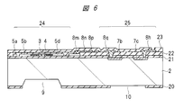
- FIG. 6 is a cross-sectional view illustrating a method for manufacturing the thermal fluid flow sensor following FIG. 5.
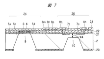
- FIG. 7 is a cross-sectional view illustrating the method for manufacturing the thermal fluid flow sensor following FIG. 6.
- FIG. 7 is a plan view (a plan view showing an enlarged part of a temperature measuring resistor) illustrating a method for manufacturing a thermal fluid flow sensor following FIG. 6. It is sectional drawing which shows the manufacturing method of the thermal type fluid flow sensor following FIG. 7 and FIG.
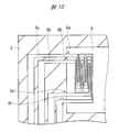
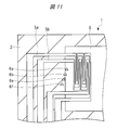
- FIG. 9 is a plan view (a plan view showing an enlarged part of a temperature measuring resistor) showing a method for manufacturing a thermal fluid flow sensor following FIG. 7 and FIG. 8; It is a top view which expands and shows a part of temperature sensing resistor which comprises the flow volume detection part of the thermal type fluid flow sensor by Example 2.
- FIG. 6 is a cross-sectional view showing a method for manufacturing a thermal fluid flow sensor according to Embodiment 3.
- FIG. It is sectional drawing which shows the manufacturing method of the thermal type fluid flow sensor following FIG.
- FIG. 15 is a cross-sectional view illustrating the method for manufacturing the thermal fluid flow sensor, continued from FIG. 14.
- FIG. 6 is a cross-sectional view of a sensor module according to a modified example of Embodiment 1.
- the constituent elements are not necessarily indispensable unless otherwise specified and clearly considered essential in principle. Needless to say.
- the thermal fluid flow sensor according to the embodiment of the present invention is a thermal fluid flow sensor that detects a fluid flow rate using a heating resistor.
- FIG. 1 is a plan view showing a sensor chip on which a thermal fluid flow sensor having a flow rate detection unit and a pressure detection unit according to the first embodiment is formed.
- the flow rate detector 24 of the thermal fluid flow sensor formed on the sensor chip 1 includes a semiconductor substrate 2 made of single crystal silicon (Si), and an insulating film formed on the upper surface of the semiconductor substrate 2. (Illustration is omitted), the heating resistor 3 formed on the insulating film, the heating resistor temperature measuring resistor 4 for detecting the temperature of the heating resistor 3, and the resistance resistors 5a, 5b, 5c, 5d.
- the resistance temperature detector 4 for the heating resistor is formed so as to surround except for a part of the periphery of the heating resistor 3.
- two pairs of resistance temperature detectors 5a and 5b are disposed on the upstream side
- two pairs of resistance temperature sensors 5c and 5d are disposed on the downstream side.
- the heating resistor 3, the heating resistor temperature measuring resistor 4, and the temperature measuring resistors 5 a, 5 b, 5 c, 5 d are disposed in a first diaphragm 9 that penetrates from the upper surface to the lower surface of the semiconductor substrate 2 in plan view. Yes.
- Markers 6a and 6f for monitoring the thickness (silicon (Si) thickness) of the second diaphragm 10 of the pressure detection unit 25 are provided in the middle of the wiring of the resistance temperature detector 5a.
- markers 6b and 6e are provided in the middle of the wiring of the resistance temperature detector 5b
- markers 6c and 6h are provided in the middle of the wiring of the resistance temperature detector 5c
- the marker 6d is provided in the middle of the wiring of the resistance temperature detector 5d.
- the protrusion of the marker 6a of the upstream resistance temperature detector 5a is located in the first diaphragm 9, and the protrusion of the marker 6b of the upstream resistance temperature detector 5b is the first diaphragm 9.
- the marker 6 f of the upstream resistance temperature detector 5 a and the protrusion of the marker 6 e of the upstream resistance temperature detector 5 b are located outside the first diaphragm 9.
- the protrusion of the marker 6c of the downstream resistance temperature detector 5c is located in the first diaphragm 9, and the protrusion of the marker 6d of the downstream resistance resistor 5d is the first
- the marker 6h of the downstream resistance temperature detector 5c and the protrusion of the marker 6g of the downstream resistance temperature detector 5d are positioned outside the first diaphragm 9 so as to overlap the end portion of the diaphragm 9. Yes. That is, the markers 6a, 6b, 6e, 6f arranged on the upstream side and the markers 6c, 6d, 6h, 6g arranged on the downstream side are arranged symmetrically.
- the pressure detection unit 25 is provided with a second diaphragm 10 having a quadrangular shape in plan view, leaving the semiconductor substrate 2 thinly processed to a constant thickness by etching. Furthermore, diffused resistors 7a, 7b, 7c, and 7d having a piezo effect are disposed along the sides of the second diaphragm 10 in the second diaphragm 10 in plan view.
- the diffusion resistors 7a, 7b, 7c, and 7d serving as pressure detection elements are n-type or p-type diffusion resistors, and are arranged so that the piezo effect can be detected to the maximum.
- the heating resistor 3 is connected to the electrode pads 8f and 8p using metal wiring in order to be electrically connected to the outside, and the heating resistor temperature measuring resistor 4 is connected to the electrode pad 8e using metal wiring. , 8p.
- the resistance temperature detectors 5a, 5b, 5c and 5d are connected to electrode pads 8a, 8b, 8c, 8d, 8j, 8k, 8m and 8n using metal wiring, and diffused resistors 7a, 7b, 7c and 7d. Are connected to electrode pads 8g, 8h, 8i, 8q, 8r, 8s using metal wiring.
- an arrow indicated by reference numeral 11 indicates the flow of air.
- the air flowing through the sensor chip 1 flows in the opposite direction to the air flow 11 or in other directions, but here, the air flows in the same direction as the air flow 11 indicated by the arrows.
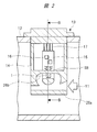
- FIG. 2 is a schematic diagram illustrating a sensor module including a sensor chip on which a thermal fluid flow sensor according to the first embodiment is formed.
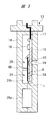
- FIG. 3 is a cross-sectional view of the sensor module along the line BB in FIG.
- a sensor module attached to an intake passage of an internal combustion engine such as an automobile is shown.
- a part of the body is shown through.
- the sensor module 13 includes a support substrate 15, a sensor chip 1 on which a thermal fluid flow sensor is formed, and an adjustment component (for example, a capacitor, etc.) 16, and the sensor The chip 1 and the adjustment component 16 are mounted on the support substrate 15.
- the support substrate 15 on which the sensor chip 1 and the adjustment component 16 are mounted is disposed in the body 14 in which the sub passages 26 a and 26 b are formed, and sends an air flow detection signal to the outside through the connector 17.
- the sub-passage 26a is branched into the sub-passage 26b in the body 14, and the sub-passage 26b branched from the sub-passage 26a is disposed on the flow rate detection unit 24 of the sensor chip 1 so that the air flow 11 can be detected.
- the partition part SB separates the area where the pressure detection part 25, the adjustment component 16 and the connector 17 are arranged.
- the support substrate 15 facing the first diaphragm 9 on the back surface side of the flow rate detection unit 24 is provided with an air flow meter through hole 18 and is connected to the sub passage 26b. Further, a pressure gauge through hole 19 is provided in the support substrate 15 and the body 14 on the back surface side of the pressure detection unit 25 and facing the second diaphragm 10. The pressure change in the intake passage 12 can be detected by the pressure gauge through hole 19.
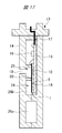
- FIG. 17 shows a cross-sectional view of a sensor module according to a modification of the first embodiment.
- a pressure gauge through hole 19 may be provided on the surface side of the sensor chip 1 to detect a pressure change in the intake passage 12.
- the metal part such as an electrode pad is exposed and covered with a resin or the like so as not to be corroded by intake air.
- the flow rate detection unit 24 of the sensor chip 1 may be disposed on the sub-passage 26a without branching.
- a control circuit for calculating and processing the analog output of the air flow rate detection signal and the pressure detection signal is not shown.
- the control circuit is mounted on the support substrate 15.
- the control circuit may be formed on the same substrate of the sensor chip 1.
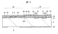
- FIGS. 4 to 7 and 9 are cross-sectional views (a cross-sectional view substantially along the line AA in FIG. 1) showing a method of manufacturing the thermal fluid flow sensor.
- FIG. 8 and FIG. 10 are plan views (a plan view showing an enlarged part of the temperature measuring resistor) showing the method for manufacturing the thermal fluid flow sensor.
- the resistance thermometer 5c, markers 6a, 6b, 6c, 6d, 6e, 6f, 6g, 6h, diffusion resistors 7a, 7d and electrode pads 8a, 8b, 8c, 8d not shown in FIGS. , 8e, 8f, 8g, 8i, 8j, 8k, 8r, 8s, etc. refer to FIG. 1 as appropriate.
- a semiconductor substrate 2 made of single crystal silicon (Si) having a crystal orientation of Si ⁇ 100> is prepared.
- the thickness of the semiconductor substrate 2 is, for example, about 400 ⁇ m.
- an impurity such as phosphorus (P) or boron (B) is doped on the upper surface of the semiconductor substrate 2 of the pressure detection unit 25 to form a pressure detection element having a predetermined depth from the upper surface of the semiconductor substrate 2.
- Diffusion resistors 7a, 7b, 7c and 7d are formed.
- the first insulating film 21 is formed on the upper surface of the semiconductor substrate 2, and the back surface insulating film 20 is formed on the lower surface (surface opposite to the upper surface) of the semiconductor substrate 2.
- the conductor film is processed to obtain a flow rate.
- the heating resistor 3, the heating resistor temperature measuring resistor 4, and the temperature measuring resistors 5 a, 5 b, 5 c, 5 d of the detection unit 24 are formed. Markers 6a, 6b, 6c, 6d, 6e, 6f, 6g, and 6h are attached to the resistance temperature detectors 5a, 5b, 5c, and 5d.
- a second insulating film is formed on the upper surface of the semiconductor substrate 2 so as to cover the heating resistor 3, the heating resistor 4 and the resistance resistors 5a, 5b, 5c, and 5d of the flow rate detector 24. 22 is formed. Note that after the second insulating film 22 is formed, the upper surface of the second insulating film 22 may be planarized by a CMP (Chemical-Mechanical-Polishing) method.
- CMP Chemical-Mechanical-Polishing
- the second insulating film 22 is processed by etching using the resist pattern as a mask, so that the heating resistor 3, the heating resistor temperature measuring resistor 4, and the temperature measuring resistors 5 a, 5 b, A connection hole CN1 reaching 5c and 5d is formed. Further, the first insulating film 21 and the second insulating film 22 are processed by etching using the resist pattern as a mask to form a connection hole CN2 reaching the diffusion resistors 7a, 7b, 7c, and 7d of the pressure detection unit 25.
- the connection holes CN1 and CN2 may be formed in the same process.
- the metal film is processed to form electrode pads 8a, 8b, 8c, 8d, 8e, 8f, 8g, 8h, 8i, 8j, 8k, 8m, 8n, 8p, 8q, 8r, 8s are formed.
- electrode pads 8f and 8p connected to the heating resistor 3 electrode pads 8e and 8p connected to the temperature measuring resistor 4 for heating resistor, and electrode pads connected to the temperature measuring resistors 5a, 5b, 5c and 5d.
- 8a, 8b, 8c, 8d, 8j, 8k, 8m, 8n and electrode pads 8g, 8h, 8i, 8q, 8r, 8s connected to the diffusion resistors 7a, 7b, 7c, 7d are formed.
- a third insulating film 23 is formed. Subsequently, the third insulating film 23 is processed by etching using the resist pattern as a mask, and the electrode pads 8a, 8b, 8c, 8d, 8e, 8f, 8g, 8h, 8i, 8j, 8k, 8m, 8n, 8p, 8q, 8r, 8s.
- a third insulating film 23 is formed. Subsequently, the third insulating film 23 is processed by etching using the resist pattern as a mask, and the electrode pads 8a, 8b, 8c, 8d, 8e, 8f, 8g, 8h, 8i, 8j, 8k, 8m, 8n, A part of 8p, 8q, 8r, and 8s that is connected to the outside is exposed.
- the back surface insulating film 20 in the region to be the first diaphragm 9 of the flow rate detection unit 24 is removed by etching using the resist pattern as a mask.
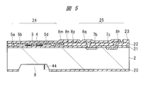
- the semiconductor substrate 2 in the region to be the first diaphragm 9 of the flow rate detection unit 24 is etched from the lower surface side of the semiconductor substrate 2 by etching using the back surface insulating film 20 as a mask.
- the first thickness 44 of the semiconductor substrate 2 is etched from the lower surface of the semiconductor substrate 2 using a solution described later.
- the first thickness 44 is a thickness obtained by adding the design thickness of the semiconductor substrate 2 of the second diaphragm 10 of the pressure detection unit 25 determined by the pressure detection range and the final finish etching amount.
- etching anisotropic etching using an alkaline solution such as a potassium hydroxide (KOH) solution or a tetramethylamide (TMAH) solution is performed.
- KOH potassium hydroxide
- TMAH tetramethylamide
- etching proceeds while maintaining a constant angle (taper), and the etching width of the semiconductor substrate 2 is gradually larger than the mask width of the back surface insulating film 20 from the lower surface to the upper surface of the semiconductor substrate 2.
- the semiconductor substrate 2 is processed so as to be narrowed.
- the crystal orientation of Si ⁇ 100> in the cross-sectional direction and the crystal orientation of Si ⁇ 111> in the oblique direction are exposed.
- the etching rate of Si ⁇ 100> is faster than the etching rate of Si ⁇ 111>, the etching proceeds while maintaining a constant angle (taper).
- the ratio between the etching amount of Si ⁇ 100> and the etching amount of Si ⁇ 111>, the so-called selection ratio, is about 10 to 40, for example.
- the selection ratio varies depending on the alkaline solution, and the selection ratio can be adjusted by adding an additive.
- the first thickness 44 is about 1 ⁇ m to 50 ⁇ m, and is small with respect to the thickness of the semiconductor substrate 2, so that etching with an alkaline solution can be performed in a short time. Thereby, there is little change in the concentration of the alkaline solution, and the semiconductor substrate 2 can be etched with high precision even with time control. At this stage, it may be once dried, and the etching amount of the semiconductor substrate 2 may be measured with a laser or the like to further improve the accuracy.
- the back surface insulating film 20 in the region that becomes the second diaphragm 10 of the pressure detection unit 25 is removed by etching using the resist pattern as a mask.
- the semiconductor substrate 2 in the region that becomes the first diaphragm 9 of the flow rate detection unit 24 and the region that becomes the second diaphragm 10 of the pressure detection unit 25 by etching using the back surface insulating film 20 as a mask. Is etched from the lower surface side of the semiconductor substrate 2.
- the etching of the semiconductor substrate 2 reaches the upper surface of the semiconductor substrate 2, and the first insulating film 21 is exposed.
- anisotropic etching is performed from the lower surface of the semiconductor substrate 2 using the alkaline solution used for etching the first thickness 44 of the semiconductor substrate 2.
- the semiconductor substrate 2 in the region to be the first diaphragm 9 of the flow rate detection unit 24 is removed by an optical microscope or the like, and the end portion of the first diaphragm 9 in contact with the first insulating film 21 from the upper surface side of the semiconductor substrate 2 is removed. Confirm that it is observed.
- the semiconductor substrate 2 in the region that becomes the first diaphragm 9 of the flow rate detection unit 24 is etched and the first insulating film 21 is exposed, the etching amount of the semiconductor substrate 2 in the region that becomes the second diaphragm 10 of the pressure detection unit 25 And the etching amount of the semiconductor substrate 2 in the region to be the first diaphragm 9 of the flow rate detection unit 24 is the same. Accordingly, the semiconductor substrate 2 having the first thickness 44 remains in the region that becomes the second diaphragm 10 of the pressure detection unit 25.
- FIG. 8 shows an enlarged plan view when the end portion of the first diaphragm 9 formed in the flow rate detection unit 24 is observed from above with an optical microscope or the like.
- the resistance temperature detectors 5a and 5b are shown in which the protruding portion of the marker 6a formed on the resistance temperature detector 5a overlaps the end portion of the first diaphragm 9.
- the other markers 6b, 6e, 6f of the resistance temperature detectors 5a, 5b are arranged so as to be shifted from the end of the first diaphragm 9 at regular intervals from the marker 6a. In this situation, the protrusions of the markers 6a, 6b, 6e, 6f are observed on the upper surface of the substrate 2.
- the final finish etching amount of the second diaphragm 10 formed in the pressure detection unit 25 is calculated, and from which selection ratio of the solution, etc., to which marker 6b, 6e, 6f the final finish etching is performed is determined.
- the etching of the crystal surface of Si ⁇ 111> proceeds by performing the final finish etching, the etching gradually proceeds in the order of the markers 6b, 6e, and 6f, and the first formed in the flow rate detection unit 24.
- the diaphragm 9 gradually increases in the horizontal direction with respect to the main surface of the semiconductor substrate 2.
- the first diaphragm 9 is formed in the flow rate detection unit 24, and the second diaphragm 10 is formed in the pressure detection unit 25.
- the etching time is calculated from the final finishing etching amount, and the final finishing etching is performed using the result, whereby the thickness of the semiconductor substrate 2 of the second diaphragm 10 formed in the pressure detection unit 25 is determined as the design thickness.
- the second thickness 45 can be accurately set.
- the first diaphragm 9 formed in the flow rate detection unit 24 does not increase in the direction perpendicular to the main surface of the semiconductor substrate 2 because the first insulating film 21 serves as a stopper, but the main surface of the semiconductor substrate 2 On the other hand, in the horizontal direction, it increases as described above. However, the mechanical strength is maintained because it is only a few ⁇ m larger.
- FIG. 10 shows an enlarged plan view when the end portion of the first diaphragm 9 formed in the flow rate detection unit 24 is observed from the upper surface with an optical microscope or the like after the final finish etching is performed.
- the protruding portion of the marker 6 b formed on the resistance temperature detector 5 b overlaps the end of the first diaphragm 9, and the first diaphragm 9 is moved in the horizontal direction of the semiconductor substrate 2 by the final finish etching. You can see that it is getting bigger.
- the interval between the marker 6a and the marker 6b can be as small as 0.1 ⁇ m, for example.
- variation in the position of the end of the first diaphragm 9 of the flow rate detection unit 24 within the wafer surface on which the plurality of sensor chips 1 are formed, that is, pressure Variations in the second thickness 45 of the second diaphragm 10 of the detection unit 25 can be inspected. If the desired markers 6b, 6d, 6e, 6f, 6g, 6h and the end of the first diaphragm 9 do not overlap, the final finish etching is added to the semiconductor substrate 2 of the second diaphragm 10. The thickness can be set to the second thickness 45 with high accuracy.
- the markers 6a, 6b, 6e, 6f and the markers 6c, 6d, 6g, 6h are formed at both ends of the first diaphragm 9 that face each other in the air flow direction. Since the amount of deviation between the flow rate detecting element and the pressure detecting element can be grasped, the detection output can be corrected. For example, the detection accuracy of the air flow rate can be improved by accurately detecting the pressure in the intake air and correcting the air flow rate.
- infrared rays when observing the end portion of the first diaphragm 9 from above, even if the first diaphragm 9 does not reach the first insulating film 21, that is, the partial thickness of the semiconductor substrate 2 is reduced. Even if it remains, when the markers 6a, 6b, 6c, 6d, 6e, 6f, 6g, and 6h are made of a metal film, infrared rays are not transmitted and the position of the end of the first diaphragm 9 is grasped. Is possible.
- the step of etching the first thickness 44 of the semiconductor substrate 2 (FIG. 5) and the step of etching the semiconductor substrate 2 leaving the second thickness 45 (FIG. 7), which are final finish etching Different solutions may be used. That is, in the step of etching the first thickness 44 of the semiconductor substrate 2 (FIG. 5), since the semiconductor substrate 2 is as thick as about 400 ⁇ m, the semiconductor substrate 2 is etched in a short time with a solution having a high selectivity. In the step of etching the semiconductor substrate 2 while leaving the second thickness 45 (FIG. 7), the markers 6a, 6b, and 6b formed on the first diaphragm 9 by etching the semiconductor substrate 2 with a solution having a low selectivity. The difference between the distances 6c, 6d, 6e, 6f, 6g, and 6h and the final finish etching amount of the second diaphragm 10 is reduced, and the second diaphragm 10 can be formed with higher accuracy.
- pressure measurement is performed using one pressure detection unit 25
- the present invention is not limited to this.
- a plurality of pressure detectors 25 having different second thicknesses 45 of the second diaphragm 10 are formed by providing markers corresponding to each pressure range in the flow rate detector 24. be able to.
- the flow rate detection unit 24 and the pressure detection unit 25 are manufactured on the same semiconductor substrate 2, so that the flow rate detection unit 24 and the pressure detection unit 25 are manufactured on different semiconductor substrates 2.
- the number of electrode pads can be reduced by sharing the wiring. Thereby, size reduction of the sensor chip 1 is realizable and reduction of manufacturing cost can be aimed at.
- the inspection cost can be reduced.
- thermo fluid flow sensor that can detect the air flow rate and the air pressure with high accuracy at low cost can be realized.
- the present Example 1 demonstrated the thermal fluid flow sensor which combined the flow volume detection element and the pressure detection element, it is not limited to this.
- a humidity detection element with a diaphragm structure formed by removing a thermal humidity detection element or a semiconductor substrate, a flow rate detection element, and a pressure detection element can be formed on the same semiconductor substrate.
- a multi-sensor capable of detecting humidity is possible.
- the inspection process can be greatly shortened, and furthermore, correction processing of each detection element can be performed, so that the cost is low, and A highly accurate thermal fluid flow sensor can be realized.
- the difference between the thermal fluid flow sensor according to the second embodiment and the thermal fluid flow sensor according to the first embodiment is the position of the marker.
- FIG. 11 is an enlarged plan view showing a part of the temperature measuring resistor constituting the flow rate detection unit of the thermal fluid flow rate sensor according to the second embodiment.
- the markers 6a, 6b, 6e, and 6f according to the first embodiment described above are formed accompanying the resistance thermometers 5a and 5b, but as shown in FIG. 11, they are attached to the resistance thermometers 5a and 5b. Instead, the markers 6a, 6b, 6e, and 6f may be arranged inside or outside the first diaphragm 9 in plan view. Even if the markers 6a, 6b, 6e, and 6f are arranged independently, the same effects as those of the first embodiment can be obtained.
- the conductor film of the same layer as the resistance temperature detectors 5a, 5b is used for the markers 6a, 6b, 6e, 6f.
- the metal of the same layer as the electrode pad is used.
- a film may be used, or a marker from which the insulating film on the semiconductor substrate 2 is removed or a marker newly formed from an insulating film may be used. Note that if only a plurality of markers are arranged, the marker corresponding to the final finish etching may not be known, and therefore a symbol may be formed in the vicinity of the marker.
- the marker is provided at the end of the first diaphragm 9.
- the marker may be disposed in an empty space of the sensor chip 1, for example, an area close to the periphery of the sensor chip 1.
- the markers 6a, 6b, 6e, and 6f are formed in a protruding shape in order to make the overlap between the markers 6a, 6b, 6e, and 6f and the end of the first diaphragm 9 easy to understand.
- a dent or the like may be formed, and any marker 6a, 6b, 6e, 6f that can recognize the overlap with the end of the first diaphragm 9 may be used.
- the difference between the thermal fluid flow sensor according to the third embodiment and the thermal fluid flow sensor according to the first embodiment is that a third diaphragm is formed also on the upper surface side of the semiconductor substrate of the flow rate detection unit. is there.
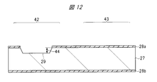
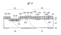
- FIGS. 12 to 15 are cross-sectional views showing a method for manufacturing the thermal fluid flow sensor of FIG.
- FIG. 16 is a plan view (a plan view showing an enlarged part of a temperature measuring resistor) showing a method for manufacturing a thermal fluid flow sensor.
- a semiconductor substrate 27 made of single crystal silicon (Si) having a crystal orientation of Si ⁇ 100> is prepared. Subsequently, a front surface insulating film 28a and a back surface insulating film 28b are formed on the upper surface and the lower surface of the semiconductor substrate 27, respectively.
- the surface insulating film 28a in the region to be the third diaphragm 29 of the flow rate detection unit 42 is removed by etching using the resist pattern as a mask.
- the semiconductor substrate 27 in the region to be the third diaphragm 29 of the flow rate detection unit 42 is etched from the upper surface side of the semiconductor substrate 27 by etching using the surface insulating film 28a as a mask.
- the first thickness 44 of the semiconductor substrate 27 is etched from the upper surface of the semiconductor substrate 27 using an alkaline solution, for example, as in the first embodiment.
- the first thickness 44 is obtained by adding the design thickness of the semiconductor substrate 27 of the second diaphragm 41 determined by the pressure detection range and the final finish etching amount.
- the upper surface of the semiconductor substrate 27 of the pressure detection unit 43 is doped with impurities such as phosphorus (P) or boron (B).
- impurities such as phosphorus (P) or boron (B).
- diffusion resistors 37b and 37c having a predetermined depth from the upper surface of the semiconductor substrate 27 and serving as pressure detection elements are formed.
- the first insulating film 31 is formed on the upper surface of the semiconductor substrate 27, and the back surface insulating film 30 is formed on the lower surface (surface opposite to the upper surface) of the semiconductor substrate 27.
- the first insulating film 31 is processed by etching using the resist pattern as a mask to form a connection hole CN3 reaching the diffusion resistors 37b and 37c.
- a conductor film such as a polycrystalline silicon (Si) film, a molybdenum (Mo) film, or a tungsten (W) film is formed on the first insulating film 31 including the inside of the connection hole CN3, the conductive film
- the body film is processed to form the heating resistor 33, the heating resistor temperature measuring resistor 34, and the temperature measuring resistors 35a, 35b, and 35d of the flow rate detector 42.
- Markers 36a, 36b, 36e, and 36f are attached to the resistance temperature detectors 35a, 35b, and 35d.
- an electrode pad PAD that is electrically connected to the diffusion resistors 37b and 37c of the pressure detection unit 43 is formed.
- the semiconductor substrate 27 is covered so as to cover the heating resistor 33 of the flow rate detection unit 42, the temperature measuring resistor 34 for the heating resistor, the temperature measuring resistors 35a, 35b, and 35d, and the electrode pad PAD of the pressure detection unit 43.
- a second insulating film 32 is formed on the upper surface. Note that after the second insulating film 32 is formed, the upper surface of the second insulating film 32 may be planarized by a CMP method.
- the second insulating film 32 is processed by etching using the resist pattern as a mask, and the heating resistor 33 of the flow rate detection unit 42, the temperature measuring resistor 34 for the heating resistor, the temperature measuring resistors 35a, 35b, A connection hole CN1 reaching 35d and the electrode pad PAD is formed.
- this metal film is processed to form electrode pads 38m, 38n, 38p, and 38h. Form.
- a third insulating film 39 is formed on the upper surface of the semiconductor substrate 27 so as to cover the electrode pads 38h, 38m, 38n, and 38p. Subsequently, the third insulating film 39 is processed by etching using the resist pattern as a mask to expose portions of the electrode pads 38h, 38m, 38n, and 38p that are connected to the outside.
- the back insulating film 30 in the region that becomes the first diaphragm 40 of the flow rate detection unit 42 and the region that becomes the second diaphragm 41 of the pressure detection unit 43 is removed by etching using the resist pattern as a mask.
- the first diaphragm 40 and the third diaphragm 29 are designed so that the first diaphragm 40 is located inside the third diaphragm 29 on the surface where the first diaphragm 40 and the third diaphragm 29 are in contact with each other. A large level difference is prevented from occurring in the diaphragm 40.
- the etching amount of the region that becomes the second diaphragm 41 of the pressure detection unit 43 is the same as the etching amount of the region that becomes the first diaphragm 40 of the flow rate detection unit 42, the first amount of the flow rate detection unit 42.
- the semiconductor substrate 27 in the region to be the diaphragm 40 is etched and the first insulating film 31 is exposed, the semiconductor substrate 27 having the first thickness 44 remains in the region to be the second diaphragm 41 of the pressure detection unit 43. Yes.
- the first diaphragm 40 is formed in the flow rate detection unit 42, and the second diaphragm 41 is formed in the pressure detection unit 43.
- the etching time is calculated from the final finishing etching amount, and the final finishing etching is performed using the result, whereby the thickness of the semiconductor substrate 27 of the second diaphragm 41 formed in the pressure detection unit 43 is determined as the design thickness.
- the second thickness 45 can be accurately set.
- the first diaphragm 40 formed in the flow rate detection unit 42 does not increase in the direction perpendicular to the main surface of the semiconductor substrate 27 because the first insulating film 31 serves as a stopper, but the main surface of the semiconductor substrate 27. On the other hand, in the horizontal direction, it increases as described above. However, the mechanical strength is maintained because it is only a few ⁇ m larger.
- FIG. 16 shows an enlarged plan view when the end portion of the first diaphragm 40 formed in the flow rate detection unit 42 is observed from the upper surface with an optical microscope or the like after the final finish etching is performed.
- the protrusion of the marker 36 b formed on the resistance temperature detector 35 b overlaps the end of the first diaphragm 40, and the first diaphragm 40 is moved in the horizontal direction of the semiconductor substrate 27 by the final finish etching. You can see that it is getting bigger.
- the pressure detection unit 43 by providing markers at both ends of the first diaphragm 40 of the flow rate detection unit 42 provided in the thermal fluid flow rate sensor, the pressure detection unit 43 The final finish etching amount of the second diaphragm 41 can be grasped. Thereby, since the 2nd diaphragm 41 which has the 2nd thickness 45 can be formed with sufficient precision, the precision improvement of pressure measurement can be aimed at.
- the flow rate detection unit 42 and the pressure detection unit 43 are fabricated on the same semiconductor substrate 27 in substantially the same manner as in the first embodiment, the flow rate detection unit 42 and the pressure detection unit 43 are provided.
- the number of electrode pads can be reduced by making the wiring common, rather than making different semiconductor substrates 27. Thereby, size reduction of a sensor chip can be implement
- the inspection cost can be reduced.
- a thermal fluid flow sensor capable of detecting the air flow rate and the air pressure with high accuracy at a low cost can be realized in substantially the same manner as in the first embodiment.
Landscapes
- Physics & Mathematics (AREA)
- General Physics & Mathematics (AREA)
- Fluid Mechanics (AREA)
- Measuring Volume Flow (AREA)
- Measuring Fluid Pressure (AREA)
- Pressure Sensors (AREA)
Abstract
低コストで、かつ、高精度の熱式流体流量センサを提供する。上記課題を解決するために、半導体基板上に流量検出部と圧力検出部とが設けられ、流量検出部は第1ダイヤフラムと、発熱抵抗体とを有し、圧力検出部は第2ダイヤフラムと、圧力検出素子となる拡散抵抗とを有する。そして、発熱抵抗体の両側にそれぞれマーカが設けられており、第2ダイヤフラムを形成する際のエッチング量をマーカで把握する。これにより、第2ダイヤフラムを精度よく形成する。
Description
本発明は、半導体装置、半導体装置の製造方法および流量センサに関する。
本技術分野の背景技術として、特開昭60-142268号公報(特許文献1)、特許第5406674号公報(特許文献2)および特許第4882732号公報(特許文献3)がある。
特開昭60-142268号公報(特許文献1)には、空気中に保持される薄膜のヒータと、空気中に保持されるとともに上記ヒータの対向する両側面に配置される1対の薄膜の熱感知センサからなる流速センサが記載されている。
特許第5406674号公報(特許文献2)には、半導体基板上に形成されたダイヤフラム内に、空気流量を検出する発熱抵抗体、発熱抵抗体用測温抵抗体および測温抵抗体と、湿度検出用発熱抵抗体を配置し、この湿度検出用発熱抵抗体上に空洞層と、空洞層上の保護膜とが形成され、保護膜に、空洞層に達する複数の孔を設けた熱式流体流量センサが記載されている。
特許第4882732号公報(特許文献3)には、半導体基板上に少なくとも発熱体が形成されて、流体の流量を検出する流量検出部が構成された半導体装置が記載されている。この半導体装置では、半導体基板の同一面側に、流量検出部と流体の湿度を検出する湿度検出部とが、湿度検出部が流量検出部よりも上流側となるように、流体の流れ方向に沿って並んで形成されている。
現在、自動車などの内燃機関の電子制御燃料噴射装置に設けられ、吸入空気量を測定する空気流量計に用いられる流体流量センサとしては、質量空気量を直接検知できることから、熱式流体流量センサが主流となっている。
この中で、特に半導体を用いたMEMS(Micro Electro Mechanical Systems:微小電気機械システム)技術により製造された熱式空気流量(エアフロー)センサ素子が、コストを低減でき、かつ、低電力で駆動できることから注目されている。
しかしながら、従来技術においては、空気流量計と湿度計との組み合わせはあるが、空気流量計と圧力計との組み合わせはなく、空気流量計における空気流量の検出精度を向上するには、圧力計を別部品として組み立てる必要がある。この場合、部品点数の増加および素子同士の配線を考慮した設計が必要となるため、構造が複雑化し、組み立て工数が増加することにより、製造コストが増大するという課題がある。
ただし、圧力計もシリコン(Si)基板を薄くしたダイヤフラムを形成するため、空気流量計と圧力計とを複合することは可能である。しかし、圧力計におけるダイヤフラムの加工に起因した感度のばらつきおよび空気流量計における空気流量の検出精度の低下などが懸念された。
上記課題を解決するために、本発明は、半導体基板の第1領域に形成された流量検出部と、半導体基板の第2領域に形成された圧力検出部と、を有する半導体装置である。流量検出部は、半導体基板の上面から下面まで貫通する第1ダイヤフラムと、平面視において第1ダイヤフラムと重なる位置に設けられた発熱抵抗体と、を有し、圧力検出部は、上面から所定の厚さの半導体基板を残して、半導体基板に設けられた第2ダイヤフラムと、平面視において第2ダイヤフラムと重なる位置に設けられた圧力検出素子と、を有する。そして、第1領域に、半導体基板の上面側の第1ダイヤフラムの端部の位置を認識することのできる複数のマーカが設けられている。
本発明によれば、低コストで、かつ、高精度の熱式流体流量センサを提供することができる。
上記した以外の課題、構成および効果は、以下の実施の形態の説明により明らかにされる。
以下の実施の形態において、便宜上その必要があるときは、複数のセクションまたは実施の形態に分割して説明するが、特に明示した場合を除き、それらはお互いに無関係なものではなく、一方は他方の一部または全部の変形例、詳細、補足説明等の関係にある。
また、以下の実施の形態において、要素の数等(個数、数値、量、範囲等を含む)に言及する場合、特に明示した場合および原理的に明らかに特定の数に限定される場合等を除き、その特定の数に限定されるものではなく、特定の数以上でも以下でも良い。
また、以下の実施の形態において、その構成要素(要素ステップ等も含む)は、特に明示した場合および原理的に明らかに必須であると考えられる場合等を除き、必ずしも必須のものではないことは言うまでもない。
また、「Aからなる」、「Aよりなる」、「Aを有する」、「Aを含む」と言うときは、特にその要素のみである旨明示した場合等を除き、それ以外の要素を排除するものでないことは言うまでもない。同様に、以下の実施の形態において、構成要素等の形状、位置関係等に言及するときは、特に明示した場合および原理的に明らかにそうでないと考えられる場合等を除き、実質的にその形状等に近似または類似するもの等を含むものとする。このことは、上記数値および範囲についても同様である。
また、以下の実施の形態を説明するための全図において、同一機能を有するものは原則として同一の符号を付し、その繰り返しの説明は省略する。また、断面図および平面図において、各部位の大きさは実デバイスと対応するものではなく、図面を分かりやすくするため、特定の部位を相対的に大きく表示する場合がある。また、断面図と平面図とが対応する場合においても、図面を分かりやすくするため、特定の部位を相対的に大きく表示する場合がある。また、断面図であっても図面を見易くするためにハッチングを省略する場合もあり、平面図であっても図面を見易くするためにハッチングを付す場合もある。
以下、本発明の実施の形態である熱式流体流量センサを、図面に基づいて詳細に説明する。本発明の実施の形態である熱式流体流量センサは、発熱抵抗体を用いて流体の流量を検出する熱式流体流量センサである。
《熱式流体流量センサの構造》
本実施例1による熱式流体流量センサの構造について、図1を用いて説明する。図1は、本実施例1による流量検出部および圧力検出部を有する熱式流体流量センサが形成されたセンサチップを示す平面図である。
本実施例1による熱式流体流量センサの構造について、図1を用いて説明する。図1は、本実施例1による流量検出部および圧力検出部を有する熱式流体流量センサが形成されたセンサチップを示す平面図である。
図1に示すように、センサチップ1に形成された熱式流体流量センサの流量検出部24は、単結晶シリコン(Si)からなる半導体基板2、半導体基板2の上面上に形成された絶縁膜(図示は省略)、当該絶縁膜上に形成された発熱抵抗体3、発熱抵抗体3の温度を検知するための発熱抵抗体用測温抵抗体4および測温抵抗体5a,5b,5c,5dを有している。
発熱抵抗体用測温抵抗体4は、発熱抵抗体3の周囲の一部を除いて囲むように形成されている。また、上流側に2対の測温抵抗体5a,5bが配置され、下流側に2対の測温抵抗体5c,5dが配置されている。発熱抵抗体3、発熱抵抗体用測温抵抗体4および測温抵抗体5a,5b,5c,5dは、平面視において半導体基板2の上面から下面まで貫通する第1ダイヤフラム9内に配置されている。
測温抵抗体5aの配線途中に、圧力検出部25の第2ダイヤフラム10の厚さ(シリコン(Si)の厚さ)をモニタするマーカ6a,6fが設けられている。同様に、測温抵抗体5bの配線途中にマーカ6b,6eを設けており、測温抵抗体5cの配線途中にマーカ6c,6hを設けており、測温抵抗体5dの配線途中にマーカ6d,6gを設けている。
例えば平面視において、上流側の測温抵抗体5aのマーカ6aの突起部は、第1ダイヤフラム9内に位置し、上流側の測温抵抗体5bのマーカ6bの突起部は、第1ダイヤフラム9の端部に重なるように位置し、上流側の測温抵抗体5aのマーカ6fおよび上流側の測温抵抗体5bのマーカ6eの突起部は、第1ダイヤフラム9の外側に位置している。
また、例えば平面視において、下流側の測温抵抗体5cのマーカ6cの突起部は、第1ダイヤフラム9内に位置し、下流側の測温抵抗体5dのマーカ6dの突起部は、第1ダイヤフラム9の端部に重なるように位置し、下流側の測温抵抗体5cのマーカ6hおよび下流側の測温抵抗体5dのマーカ6gの突起部は、第1ダイヤフラム9の外側に位置している。すなわち、上流側に配置されたマーカ6a,6b,6e,6fと、下流側に配置されたマーカ6c,6d,6h,6gとは対称に配置されている。
圧力検出部25には、エッチングにより一定の厚さに薄く加工した半導体基板2を残して、平面視において四角形状の第2ダイヤフラム10が設けられている。さらに、平面視において第2ダイヤフラム10内には、第2ダイヤフラム10の各辺に沿って、ピエゾ効果を有する拡散抵抗7a,7b,7c,7dがそれぞれ配置されている。圧力検出素子となる拡散抵抗7a,7b,7c,7dは、n型またはp型の拡散抵抗であり、ピエゾ効果が最大に検出できるように配置されている。
さらに、外部と電気的に接続するため、発熱抵抗体3は、金属配線を用いた電極パッド8f,8pに接続され、発熱抵抗体用測温抵抗体4は、金属配線を用いた電極パッド8e,8pに接続されている。また、測温抵抗体5a,5b,5c,5dは、金属配線を用いた電極パッド8a,8b,8c,8d,8j,8k,8m,8nに接続され、拡散抵抗7a,7b,7c,7dは、金属配線を用いた電極パッド8g,8h,8i,8q,8r,8sに接続されている。
図1において、符号11で示す矢印は、空気の流れを示す。センサチップ1を流れる空気は、場合によっては空気の流れ11と逆方向に流れる、または、それ以外の方向へ流れることもあるが、ここでは、矢印で示す空気の流れ11と同じ方向に流れるものとする。
《センサモジュール(熱式空気流量計)の構造》
本実施例1によるセンサモジュールの構造について、図2および図3を用いて説明する。図2は、本実施例1による熱式流体流量センサが形成されたセンサチップを搭載するセンサモジュールを示す模式図である。図3は、図2のB-B線に沿ったセンサモジュールの断面図である。図2では、自動車などの内燃機関の吸気通路に取り付けられたセンサモジュールを図示しており、センサモジュールの構造をわかりやすくするため、ボディの一部を透過させて図示している。
本実施例1によるセンサモジュールの構造について、図2および図3を用いて説明する。図2は、本実施例1による熱式流体流量センサが形成されたセンサチップを搭載するセンサモジュールを示す模式図である。図3は、図2のB-B線に沿ったセンサモジュールの断面図である。図2では、自動車などの内燃機関の吸気通路に取り付けられたセンサモジュールを図示しており、センサモジュールの構造をわかりやすくするため、ボディの一部を透過させて図示している。
図2および図3に示すように、センサモジュール13は、支持基板15と、熱式流体流量センサが形成されたセンサチップ1と、調整部品(例えばコンデンサ、など)16と、を有し、センサチップ1および調整部品16は支持基板15上に搭載されている。センサチップ1および調整部品16を搭載した支持基板15は、副通路26a、26bが形成されたボディ14内に配置され、コネクタ17を通して外部へ空気流量検出信号を送っている。
副通路26aは、ボディ14内で副通路26bに分岐し、副通路26aから分岐した副通路26bは、センサチップ1の流量検出部24上に空気の流れ11が検出できるように配置され、センサ仕切り部SBによって、圧力検出部25、調整部品16およびコネクタ17が配置された領域と分離されている。
流量検出部24の裏面側で、かつ、第1ダイヤフラム9と対向する支持基板15には空気流量計用貫通穴18が設けられており、副通路26b内とつながっている。また、圧力検出部25の裏面側で、かつ、第2ダイヤフラム10と対向する支持基板15およびボディ14に圧力計用貫通穴19が設けられている。圧力計用貫通穴19により吸気通路12内の圧力変化を検出することができる。
図17に、本実施の形態1の変形例によるセンサモジュールの断面図を示す。図17に示すように、センサチップ1の表面側に圧力計用貫通穴19を設けて、吸気通路12内の圧力変化を検出してもよい。その場合には、電極パッドなど金属部が露出し、吸気によって腐食しないように、当該金属部を樹脂などで覆う。
本実施例1では、副通路26aが副通路26bに分岐している例を記載したが、分岐せず副通路26a上にセンサチップ1の流量検出部24を配置してもよい。また、本実施例1では、空気流量検出信号および圧力検出信号のアナログ出力を演算処理する制御回路を図示していないが、調整部品16と同様、支持基板15上に当該制御回路を搭載してもよく、または、センサチップ1の同一基板上に当該制御回路を形成してもよい。
また、図1に示した電極パッド8a,8b,8c,8d,8e,8f,8g,8h,8i,8j,8k,8m,8n,8p,8q,8r,8sは、副通路26bに露出すると腐食するため、少なくとも第1ダイヤフラム9より圧力検出部25に近い領域に配置することが望ましい。
《熱式流体流量センサの製造方法》
次に、本実施例1による熱式流体流量センサの製造方法について、図4~図10を用いて工程順に説明する。図4~図7および図9は、熱式流体流量センサの製造方法を示す断面図(図1のA-A線に略沿った断面図)である。図8および図10は、熱式流体流量センサの製造方法を示す平面図(温測抵抗体の一部を拡大して示す平面図)である。なお、図4~図10に記載されていない温測抵抗体5c、マーカ6a,6b,6c,6d,6e,6f,6g,6h、拡散抵抗7a,7dおよび電極パッド8a,8b,8c,8d,8e,8f,8g,8i,8j,8k,8r,8sなどは、適宜図1を参照する。
次に、本実施例1による熱式流体流量センサの製造方法について、図4~図10を用いて工程順に説明する。図4~図7および図9は、熱式流体流量センサの製造方法を示す断面図(図1のA-A線に略沿った断面図)である。図8および図10は、熱式流体流量センサの製造方法を示す平面図(温測抵抗体の一部を拡大して示す平面図)である。なお、図4~図10に記載されていない温測抵抗体5c、マーカ6a,6b,6c,6d,6e,6f,6g,6h、拡散抵抗7a,7dおよび電極パッド8a,8b,8c,8d,8e,8f,8g,8i,8j,8k,8r,8sなどは、適宜図1を参照する。
まず、図4に示すように、Si<100>の結晶方位を有する単結晶シリコン(Si)からなる半導体基板2を用意する。半導体基板2の厚さは、例えば400μm程度である。続いて、圧力検出部25の半導体基板2の上面に、リン(P)またはボロン(B)などの不純物をドーピングして、半導体基板2の上面から所定の深さを有する、圧力検出素子となる拡散抵抗7a,7b,7c,7dを形成する。続いて、半導体基板2の上面上に第1絶縁膜21を形成し、半導体基板2の下面(上面と反対側の面)上に裏面絶縁膜20を形成する。
次に、第1絶縁膜21上に導電体膜、例えば多結晶シリコン(Si)膜、モリブデン(Mo)膜またはタングステン(W)膜などを形成した後、この導電体膜を加工して、流量検出部24の発熱抵抗体3、発熱抵抗体用測温抵抗体4および測温抵抗体5a,5b,5c,5dを形成する。測温抵抗体5a,5b,5c,5dには、マーカ6a,6b,6c,6d,6e,6f,6g,6hが付随している。
次に、流量検出部24の発熱抵抗体3、発熱抵抗体用測温抵抗体4および測温抵抗体5a,5b,5c,5dを覆うように、半導体基板2の上面上に第2絶縁膜22を形成する。なお、第2絶縁膜22を形成した後、CMP(Chemical Mechanical Polishing)法により第2絶縁膜22の上面の平坦化を行ってもよい。
次に、レジストパターンをマスクとしたエッチングにより、第2絶縁膜22を加工して、流量検出部24の発熱抵抗体3、発熱抵抗体用測温抵抗体4および測温抵抗体5a,5b,5c,5dに達する接続孔CN1を形成する。また、レジストパターンをマスクとしたエッチングにより、第1絶縁膜21および第2絶縁膜22を加工して、圧力検出部25の拡散抵抗7a,7b,7c,7dに達する接続孔CN2を形成する。接続孔CN1,CN2は同一の工程で形成してもよい。
次に、接続孔CN1,CN2の内部を含む第2絶縁膜22上に金属膜、例えばアルミニウム(Al)膜などを形成した後、この金属膜を加工して、電極パッド8a,8b,8c,8d,8e,8f,8g,8h,8i,8j,8k,8m,8n,8p,8q,8r,8sを形成する。
これにより、発熱抵抗体3に接続する電極パッド8f,8p、発熱抵抗体用測温抵抗体4に接続する電極パッド8e,8p、測温抵抗体5a,5b,5c,5dに接続する電極パッド8a,8b,8c,8d,8j,8k,8m,8n、拡散抵抗7a,7b,7c,7dに接続する電極パッド8g,8h,8i,8q,8r,8sが形成される。
次に、電極パッド8a,8b,8c,8d,8e,8f,8g,8h,8i,8j,8k,8m,8n,8p,8q,8r,8sを覆うように、半導体基板2の上面上に第3絶縁膜23を形成する。続いて、レジストパターンをマスクとしたエッチングにより、第3絶縁膜23を加工して、電極パッド8a,8b,8c,8d,8e,8f,8g,8h,8i,8j,8k,8m,8n,8p,8q,8r,8sの一部であって、外部と接続する部分を露出させる。
次に、レジストパターンをマスクとしたエッチングにより、流量検出部24の第1ダイヤフラム9となる領域の裏面絶縁膜20を除去する。
次に、図5に示すように、裏面絶縁膜20をマスクとしたエッチングにより、流量検出部24の第1ダイヤフラム9となる領域の半導体基板2を、半導体基板2の下面側からエッチングする。
この際、後述の溶液を用いて、半導体基板2の下面から半導体基板2の第1厚さ44をエッチングする。第1厚さ44は、圧力検出のレンジにより決まる圧力検出部25の第2ダイヤフラム10の半導体基板2の設計厚さと最終仕上げエッチング量とを加えた厚さとなる。
このエッチングでは、例えば水酸化カリウム(KOH)溶液またはテトラメチルアミド(TMAH:Tetramethylammonium hydroxide)溶液などのアルカリ系溶液を用いた異方性エッチングを行う。これにより、一定の角度(テーパ)を保ったまま、エッチングが進行していき、半導体基板2の下面から上面に向かって、半導体基板2のエッチング幅が裏面絶縁膜20のマスク幅よりも徐々に狭くなるように、半導体基板2は加工される。
アルカリ系溶液による半導体基板2のエッチングでは、断面方向のSi<100>の結晶方位と斜め方向のSi<111>の結晶方位が露出する。通常、Si<100>のエッチング速度は、Si<111>のエッチング速度より速いことから、一定の角度(テーパ)を保ったまま、エッチングが進行する。
Si<100>のエッチング量とSi<111>のエッチング量との比、いわゆる選択比は、例えば10~40程度である。当該選択比は、アルカリ系溶液により異なり、また、添加剤を加えることにより、当該選択比を調整することができる。
第1厚さ44は、1μm~50μm程度であり、半導体基板2の厚さに対して小さいため、短時間でアルカリ系溶液によるエッチングを行うことができる。これにより、アルカリ系溶液の濃度変化が少なく、時間制御でも精度よく半導体基板2をエッチングすることができる。なお、この段階で、一度乾燥させ、レーザなどにより半導体基板2のエッチング量を計測し、さらに精度を高めてもよい。
次に、図6に示すように、レジストパターンをマスクとしたエッチングにより、圧力検出部25の第2ダイヤフラム10となる領域の裏面絶縁膜20を除去する。
次に、図7に示すように、裏面絶縁膜20をマスクとしたエッチングにより、流量検出部24の第1ダイヤフラム9となる領域および圧力検出部25の第2ダイヤフラム10となる領域の半導体基板2を、半導体基板2の下面側からエッチングする。これにより、流量検出部24の第1ダイヤフラム9となる領域では、半導体基板2のエッチングは、半導体基板2の上面に達し、第1絶縁膜21が露出する。
この際、半導体基板2の第1厚さ44をエッチングする際に用いたアルカリ系溶液を用いて、半導体基板2の下面から異方性エッチングを行う。
ここで、光学顕微鏡などで、流量検出部24の第1ダイヤフラム9となる領域の半導体基板2が除去され、半導体基板2の上面側から第1絶縁膜21に接する第1ダイヤフラム9の端部が観察されることを確認する。流量検出部24の第1ダイヤフラム9となる領域の半導体基板2がエッチングされて第1絶縁膜21が露出した時点では、圧力検出部25の第2ダイヤフラム10となる領域の半導体基板2のエッチング量と、流量検出部24の第1ダイヤフラム9となる領域の半導体基板2のエッチング量とは同じである。従って、圧力検出部25の第2ダイヤフラム10となる領域には、第1厚さ44の半導体基板2が残っている。
図8に、流量検出部24に形成された第1ダイヤフラム9の端部を上面から光学顕微鏡などで観察したときの拡大平面図を示す。一例として、測温抵抗体5aに形成されたマーカ6aの突起部が第1ダイヤフラム9の端部と重なっている温測抵抗体5a,5bを示している。
図8に示すように、温測抵抗体5a,5bの他のマーカ6b,6e,6fは、マーカ6aから一定間隔で第1ダイヤフラム9の端部から離れる方向にずらして配置しており、半導体基板2の上面上にマーカ6a,6b,6e,6fの突起部が観察される状況である。
この段階で、圧力検出部25に形成される第2ダイヤフラム10の最終仕上げエッチング量を計算し、溶液の選択比などから、どのマーカ6b,6e,6fまで最終仕上げエッチングを行うかを決定する。なお、最終仕上げエッチングを行うことにより、Si<111>の結晶面のエッチングが進行すると、マーカ6b,6e,6fの順にエッチングは徐々に進行していき、流量検出部24に形成された第1ダイヤフラム9は、半導体基板2の主面に対して水平方向に徐々に大きくなっていく。
次に、図9に示すように、最終仕上げエッチングを行うことにより、流量検出部24に第1ダイヤフラム9が形成され、圧力検出部25に第2ダイヤフラム10が形成される。最終仕上げエッチング量からエッチング時間を計算し、その結果を用いて追加の最終仕上げエッチングを行うことにより、圧力検出部25に形成された第2ダイヤフラム10の半導体基板2の厚さを、設計厚さである第2厚さ45に精度よく設定することができる。
なお、流量検出部24に形成された第1ダイヤフラム9は、第1絶縁膜21がストッパとなるので、半導体基板2の主面に対して垂直方向には大きくならないが、半導体基板2の主面に対して水平方向には、前述したように大きくなる。ただし、数μm程度大きくなるだけなので機械的強度は維持されたままである。
図10に、最終仕上げエッチングを行った後における、流量検出部24に形成された第1ダイヤフラム9の端部を上面から光学顕微鏡などで観察したときの拡大平面図を示す。
図10に示すように、測温抵抗体5bに形成されたマーカ6bの突起部が第1ダイヤフラム9の端部と重なっており、最終仕上げエッチングにより第1ダイヤフラム9が半導体基板2の水平方向において大きくなっていることがわかる。なお、マーカ6aとマーカ6bとの間隔は、例えば最小では0.1μmまで可能である。
この段階で、寸法測定が可能な画像認識検査装置を用いれば、複数のセンサチップ1が形成されるウエハ面内における流量検出部24の第1ダイヤフラム9の端部の位置のばらつき、すなわち、圧力検出部25の第2ダイヤフラム10の第2厚さ45のばらつきを検査することができる。また、所望のマーカ6b,6d,6e,6f,6g,6hと第1ダイヤフラム9の端部とが重なっていない場合は、最終仕上げエッチングを追加することにより、第2ダイヤフラム10の半導体基板2の厚さを、第2厚さ45に精度よく設定することができる。
また、図1に示したように、マーカ6a,6b,6e,6fとマーカ6c,6d,6g,6hとをそれぞれ、第1ダイヤフラム9の空気が流れる方向に対向する両端部に形成することにより、流量検出素子と圧力検出素子とのずれ量を把握することができるので、検出出力の補正が可能となる。例えば吸入空気中の圧力を精度よく検出し、空気流量を補正することにより、空気流量の検出精度を高めることができる。
また、第1ダイヤフラム9の端部を上面から観察する際に赤外線を用いることにより、第1ダイヤフラム9が第1絶縁膜21に達していなくても、すなわち、半導体基板2の一部厚さが残っていても、マーカ6a,6b,6c,6d,6e,6f,6g,6hを金属膜から構成した場合は、赤外線は透過せず、第1ダイヤフラム9の端部との位置を把握することが可能である。
また、半導体基板2の第1厚さ44をエッチングする工程(図5)と、最終仕上げエッチングである、第2厚さ45を残して半導体基板2をエッチングする工程(図7)とにおいて、互いに異なる溶液を用いてもよい。すなわち、半導体基板2の第1厚さ44をエッチングする工程(図5)では、半導体基板2が約400μm程度と厚いため、選択比の高い溶液で、短時間で半導体基板2をエッチングする。また、第2厚さ45を残して半導体基板2をエッチングする工程(図7)では、選択比の低い溶液で半導体基板2をエッチングすることにより、第1ダイヤフラム9に形成したマーカ6a,6b,6c,6d,6e,6f,6g,6hの間隔と、第2ダイヤフラム10の最終仕上げエッチング量との差が小さくなり、より精度良く、第2ダイヤフラム10を形成することができる。
また、本実施例1では、1つの圧力検出部25を用いて圧力測定を行う場合を記載しているが、これに限定されるものではない。例えばダイナミックレンジで圧力測定を行う場合は、流量検出部24に各圧力レンジに対応するマーカを設けることにより、第2ダイヤフラム10の第2厚さ45が互いに異なる複数の圧力検出部25を形成することができる。
《本実施例1による熱式流体流量センサの効果》
本実施例1では、熱式流体流量センサに備わる流量検出部24の第1ダイヤフラム9の両端部にそれぞれマーカ6a,6b,6e,6fとマーカ6c,6d,6g,6hとを設けることにより、圧力検出部25の第2ダイヤフラム10の最終仕上げエッチング量を把握することができる。これにより、精度よく、第2厚さ45を有する第2ダイヤフラム10を形成することができるので、圧力計測の精度向上を図ることができる。さらに、精度よく検出した圧力を用いて空気流用を補正することにより、空気流量計測の精度向上を図ることができる。
本実施例1では、熱式流体流量センサに備わる流量検出部24の第1ダイヤフラム9の両端部にそれぞれマーカ6a,6b,6e,6fとマーカ6c,6d,6g,6hとを設けることにより、圧力検出部25の第2ダイヤフラム10の最終仕上げエッチング量を把握することができる。これにより、精度よく、第2厚さ45を有する第2ダイヤフラム10を形成することができるので、圧力計測の精度向上を図ることができる。さらに、精度よく検出した圧力を用いて空気流用を補正することにより、空気流量計測の精度向上を図ることができる。
また、本実施例1では、流量検出部24および圧力検出部25を同一の半導体基板2に作製しているので、流量検出部24および圧力検出部25をそれぞれ異なる半導体基板2に作製するよりも、配線の共通化により電極パッドの数を削減することができる。これにより、センサチップ1の小型化が実現でき、製造コストの低減を図ることができる。また、流量検出部24の検査と圧力検出部25の検査とを同時にできるので、検査コストの低減を図ることができる。
従って、本実施例1では、低コストで、かつ、空気流量および空気圧力を高精度で検出することのできる熱式流体流量センサを実現することができる。
なお、本実施例1では、流量検出素子と圧力検出素子とを組み合わせた熱式流体流量センサに関して説明したが、これに限定されるものではない。例えば熱式の湿度検出素子または半導体基板を除去して形成するダイヤフラム構造の湿度検出素子と、流量検出素子と、圧力検出素子とを同一の半導体基板に形成することができ、流量検出、圧力検出および湿度検出が検出可能なマルチセンサが可能である。また、マルチセンサに制御回路を搭載して、1つのセンサチップとすることにより、検査工程を大幅に短縮することができ、さらに、各検出素子の補正処理が行えるので、低コストで、かつ、高精度の熱式流体流量センサを実現することができる。
本実施例2による熱式流体流量センサと、前述の実施例1による熱式流体流量センサとが異なる点は、マーカの位置である。
本実施例2による熱式流体流量センサの構造について、図11を用いて以下に説明する。図11は、本実施例2による熱式流体流量センサの流量検出部を構成する温測抵抗体の一部を拡大して示す平面図である。
前述の実施例1によるマーカ6a,6b,6e,6fは、測温抵抗体5a,5bに付随して形成されていたが、図11に示すように、測温抵抗体5a,5bに付随せず、単独でマーカ6a,6b,6e,6fを平面視において第1ダイヤフラム9の内または外に配置してもよい。単独でマーカ6a,6b,6e,6fを配置しても、前述の実施例1とほぼ同様の効果が得られる。
また、前述の実施例1では、マーカ6a,6b,6e,6fに測温抵抗体5a,5bと同一層の導電体膜を用いたが、本実施例2では、電極パッドと同一層の金属膜を用いてもよく、あるいは、半導体基板2上の絶縁膜を除去したマーカまたは新たに絶縁膜で形成したマーカであってもいい。なお、複数のマーカのみを配置すると、最終仕上げエッチングに対応するマーカが判らなくなるおそれがあるため、マーカの近辺に記号を形成してもよい。
また、本実施例2では、第1ダイヤフラム9の端部にマーカを設けているが、センサチップ1の空きスペース、例えばセンサチップ1の周縁に近い領域などに配置してもよく、このように配置することにより、マーカのレイアウトの自由度が向上する。
なお、本実施例2では、マーカ6a,6b,6e,6fと第1ダイヤフラム9の端部との重なりを分かりやすくするため、マーカ6a,6b,6e,6fを突起形状としたが、尖った凹みなどを形成してもよく、第1ダイヤフラム9の端部との重なりを認識できるマーカ6a,6b,6e,6fであればよい。
本実施例3による熱式流体流量センサと、前述の実施例1による熱式流体流量センサとが異なる点は、流量検出部の半導体基板の上面側にも第3ダイヤフラムを形成していることである。
本実施例3による熱式流体流量センサの製造方法を、図12~図16を用いて工程順に説明する。図12~図15は、図1の熱式流体流量センサの製造方法を示す断面図である。図16は、熱式流体流量センサの製造方法を示す平面図(温測抵抗体の一部を拡大して示す平面図)である。
まず、図12に示すように、Si<100>の結晶方位を有する単結晶シリコン(Si)からなる半導体基板27を用意する。続いて、半導体基板27の上面および下面にそれぞれ表面絶縁膜28aおよび裏面絶縁膜28bを形成する。
次に、レジストパターンをマスクとしたエッチングにより、流量検出部42の第3ダイヤフラム29となる領域の表面絶縁膜28aを除去する。
次に、表面絶縁膜28aをマスクとしたエッチングにより、流量検出部42の第3ダイヤフラム29となる領域の半導体基板27を、半導体基板27の上面側からエッチングする。
この際、前述の実施例1と同様に、例えばアルカリ系溶液を用いて、半導体基板27の上面から半導体基板27の第1厚さ44をエッチングする。第1厚さ44は、圧力検出のレンジにより決まる第2ダイヤフラム41の半導体基板27の設計厚さと最終仕上げエッチング量とを加えた厚さとなる。
次に、図13示すように、表面絶縁膜28aおよび裏面絶縁膜28bを除去した後、圧力検出部43の半導体基板27の上面に、リン(P)またはボロン(B)などの不純物をドーピングして、半導体基板27の上面から所定の深さを有する、圧力検出素子となる拡散抵抗37b,37cを形成する。続いて、半導体基板27の上面上に第1絶縁膜31を形成し、半導体基板27の下面(上面と反対側の面)上に裏面絶縁膜30を形成する。
次に、レジストパターンをマスクとしたエッチングにより、第1絶縁膜31を加工して、拡散抵抗37b,37cに達する接続孔CN3を形成する。
次に、接続孔CN3の内部を含む第1絶縁膜31上に、導電体膜、例えば多結晶シリコン(Si)膜、モリブデン(Mo)膜またはタングステン(W)膜などを形成した後、この導電体膜を加工して、流量検出部42の発熱抵抗体33、発熱抵抗体用測温抵抗体34および測温抵抗体35a,35b,35dを形成する。測温抵抗体35a,35b,35dには、マーカ36a,36b,36e,36f(図16参照)が付随している。さらに、圧力検出部43の拡散抵抗37b,37cと電気的に接続する電極パッドPADを形成する。
次に、流量検出部42の発熱抵抗体33、発熱抵抗体用測温抵抗体34および測温抵抗体35a,35b,35d並びに圧力検出部43の電極パッドPADを覆うように、半導体基板27の上面上に第2絶縁膜32を形成する。なお、第2絶縁膜32を形成した後、CMP法により第2絶縁膜32の上面の平坦化を行ってもよい。
次に、レジストパターンをマスクとしたエッチングにより、第2絶縁膜32を加工して、流量検出部42の発熱抵抗体33、発熱抵抗体用測温抵抗体34、測温抵抗体35a,35b,35dおよび電極パッドPADに達する接続孔CN1を形成する。
次に、接続孔CN1の内部を含む第2絶縁膜32上に金属膜、例えばアルミニウム(Al)膜などを形成した後、この金属膜を加工して、電極パッド38m,38n,38p,38hを形成する。
これにより、発熱抵抗体33に接続する電極パッド38p、発熱抵抗体用測温抵抗体34に接続する電極パッド38p、測温抵抗体35a,35b,35dに接続する電極パッド38m,38n、拡散抵抗37b,37cに接続する電極パッド38hが形成される。
次に、電極パッド38h,38m,38n,38pを覆うように、半導体基板27の上面上に第3絶縁膜39を形成する。続いて、レジストパターンをマスクとしたエッチングにより、第3絶縁膜39を加工して、電極パッド38h,38m,38n,38pの一部であって、外部と接続する部分を露出させる。
次に、レジストパターンをマスクとしたエッチングにより、流量検出部42の第1ダイヤフラム40となる領域および圧力検出部43の第2ダイヤフラム41となる領域の裏面絶縁膜30を除去する。
次に、図14に示すように、裏面絶縁膜30をマスクとしたエッチングにより、流量検出部42の第1ダイヤフラム40となる領域および圧力検出部43の第2ダイヤフラム41となる領域の半導体基板27を、半導体基板27の下面側から、前述の実施例1で説明したアルカリ系溶液を用いて異方性エッチングを行う。これにより、流量検出部42の第1ダイヤフラム40となる領域では、半導体基板27のエッチングは、半導体基板27の上面(第3ダイヤフラム29)に達し、第1絶縁膜31が露出する。
なお、第1ダイヤフラム40と第3ダイヤフラム29とが接する面において、第1ダイヤフラム40が第3ダイヤフラム29よりも内側に位置するように、第1ダイヤフラム40および第3ダイヤフラム29を設計し、第1ダイヤフラム40内に大きな段差が発生しないようにする。
この際、圧力検出部43の第2ダイヤフラム41となる領域のエッチング量と流量検出部42の第1ダイヤフラム40となる領域とのエッチング量とは同じであることから、流量検出部42の第1ダイヤフラム40となる領域の半導体基板27がエッチングされて第1絶縁膜31が露出した時点で、圧力検出部43の第2ダイヤフラム41となる領域には第1厚さ44の半導体基板27が残っている。
次に、前述の実施例1と同様に、流量検出部42の第1ダイヤフラム40の端部が、どのマーカの突起部と重なっているかを確認し、最終仕上げエッチング量からエッチング時間を形成する。
次に、図15に示すように、最終仕上げエッチングを行うことにより、流量検出部42に第1ダイヤフラム40が形成され、圧力検出部43に第2ダイヤフラム41が形成される。最終仕上げエッチング量からエッチング時間を計算し、その結果を用いて追加の最終仕上げエッチングを行うことにより、圧力検出部43に形成された第2ダイヤフラム41の半導体基板27の厚さを、設計厚さである第2厚さ45に、精度よく設定することができる。
なお、流量検出部42に形成された第1ダイヤフラム40は、第1絶縁膜31がストッパとなるので、半導体基板27の主面に対して垂直方向には大きくならないが、半導体基板27の主面に対して水平方向には、前述したように大きくなる。ただし、数μm程度大きくなるだけなので機械的強度は維持されたままである。
図16に、最終仕上げエッチングを行った後における、流量検出部42に形成された第1ダイヤフラム40の端部を上面から光学顕微鏡などで観察したときの拡大平面図を示す。
図16に示すように、測温抵抗体35bに形成されたマーカ36bの突起部が第1ダイヤフラム40の端部と重なっており、最終仕上げエッチングにより第1ダイヤフラム40が半導体基板27の水平方向において大きくなっていることがわかる。
従って、本実施例3では、前述の実施例1とほぼ同様に、熱式流体流量センサに備わる流量検出部42の第1ダイヤフラム40の両端部にそれぞれマーカを設けることにより、圧力検出部43の第2ダイヤフラム41の最終仕上げエッチング量を把握することができる。これにより、精度よく、第2厚さ45を有する第2ダイヤフラム41を形成することができるので、圧力計測の精度向上を図ることができる。
また、本実施例3では、前述の実施例1とほぼ同様に、流量検出部42および圧力検出部43を同一の半導体基板27に作製しているので、流量検出部42および圧力検出部43をそれぞれ異なる半導体基板27に作製するよりも、配線の共通化により電極パッドの数を削減することができる。これにより、センサチップの小型化が実現でき、製造コストの低減を図ることができる。また、流量検出部42の検査と圧力検出部43の検査とを同時にできるので、検査コストの低減を図ることができる。
従って、本実施例3では、前述の実施例1とほぼ同様に、低コストで、かつ、空気流量および空気圧力を高精度に検出することのできる熱式流体流量センサを実現することができる。
以上、本発明者らによってなされた発明を実施の形態に基づき具体的に説明したが、本発明は前記実施の形態に限定されるものではなく、その要旨を逸脱しない範囲で種々変更可能であることはいうまでもない。
1 センサチップ
2 半導体基板
3 発熱抵抗体
4 発熱抵抗体用測温抵抗体
5a,5b,5c,5d 測温抵抗体
6a,6b,6c,6d,6e,6f,6g,6h マーカ
7a,7b,7c,7d 拡散抵抗
8a,8b,8c,8d,8e,8f,8g,8h,8i 電極パッド
8j,8k,8m,8n,8p,8q,8r,8s 電極パッド
9 第1ダイヤフラム
10 第2ダイヤフラム
11 空気の流れ
12 吸気通路
13 センサモジュール
14 ボディ
15 支持基板
16 調整部品
17 コネクタ
18 空気流量計用貫通穴
19 圧力計用貫通穴
20 裏面絶縁膜
21 第1絶縁膜
22 第2絶縁膜
23 第3絶縁膜
24 流量検出部
25 圧力検出部
26a,26b 副通路
27 半導体基板
28a 表面絶縁膜
28b 裏面絶縁膜
29 第3ダイヤフラム
30 裏面絶縁膜
31 第1絶縁膜
32 第2絶縁膜
33 発熱抵抗体
34 発熱抵抗体用測温抵抗体
35a,35b,35d 測温抵抗体
36a,36b,36e,36f マーカ
37b,37c 拡散抵抗
38h,38m,38n,38p 電極パッド
39 第3絶縁膜
40 第1ダイヤフラム
41 第2ダイヤフラム
42 流量検出部
43 圧力検出部
44 第1厚さ
45 第2厚さ
CN1,CN2,CN3 接続孔
PAD 電極パッド
SB センサ仕切り部
Claims (15)
- 上面および前記上面と反対側の下面を有する、第1厚さの基板と、
前記基板の第1領域に形成された第1センサ部と、
前記基板の前記第1領域とは異なる第2領域に形成された第2センサ部と、
を有し、
前記第1センサ部は、
前記基板の前記上面から前記下面まで貫通する第1開口と、
平面視において前記第1開口と重なる位置に設けられた第1検出素子と、
を有し、
前記第2センサ部は、
前記上面側に前記第1厚さよりも薄い第2厚さの前記基板を残して、前記下面側に設けられた第2開口と、
平面視において前記第2開口と重なる位置に設けられた第2検出素子と、
を有し、
前記第1領域に、前記第1開口の前記上面側の端部の位置を認識することのできる複数のマーカが設けられている、半導体装置。 - 請求項1記載の半導体装置において、
前記複数のマーカは、前記第1検出素子を挟んで対称となるように配置された、第1のマーカ群と第2のマーカ群とから構成される、半導体装置。 - 請求項1記載の半導体装置において、
前記複数のマーカは、第1導電体膜から構成され、前記第1検出素子は、第2導電体膜から構成され、前記第1導電体膜と前記第2導電体膜とは同一層である、半導体装置。 - 請求項1記載の半導体装置において、
前記複数のマーカは、前記第1開口の前記上面側の前記端部からの距離が互いに異なる位置にそれぞれ設けられている、半導体装置。 - 請求項1記載の半導体装置において、
前記第1検出素子は、空気流量を検出する発熱抵抗体であり、前記第2検出素子は、圧力検出素子である、半導体装置。 - 上面および前記上面と反対側の下面を有する、第1厚さの基板と、
前記基板の第1領域に形成された第1センサ部と、
前記基板の前記第1領域とは異なる第2領域に形成された第2センサ部と、
を有し、
前記第1センサ部は、
前記基板の前記上面側に設けられ、第1底面を有する第1開口と、
前記基板の前記下面側の前記第1開口に対向する位置に設けられ、前記第1底面に接する第2底面を有する第2開口と、
平面視において前記第1開口と重なる位置に設けられた第1検出素子と、
を有し、
前記第2センサ部は、
前記上面側に前記第1厚さよりも薄い第2厚さの前記基板を残して、前記下面側に設けられた第3開口と、
平面視において前記第3開口と重なる位置に設けられた第2検出素子と、
を有し、
前記第1領域に、前記第2開口の前記上面側の端部の位置を認識することのできる複数のマーカが設けられている、半導体装置。 - 請求項6記載の半導体装置において、
前記複数のマーカは、前記第1検出素子を挟んで対称となるように配置された、第1のマーカ群と第2のマーカ群とから構成される、半導体装置。 - 請求項6記載の半導体装置において、
前記複数のマーカは、第1導電体膜から構成され、前記第1検出素子は、第2導電体膜から構成され、前記第1導電体膜と前記第2導電体膜とは同一層である、半導体装置。 - 請求項6記載の半導体装置において、
前記複数のマーカは、前記第2開口の前記上面側の前記端部からの距離が互いに異なる位置にそれぞれ設けられている、半導体装置。 - 請求項6記載の半導体装置において、
前記第1検出素子は、空気流量を検出する発熱抵抗体であり、前記第2検出素子は、圧力検出素子である、半導体装置。 - 請求項6記載の半導体装置において、
前記第2開口の前記第2底面は前記第1開口の前記第1底面の内側に位置する、半導体装置。 - (a)基板の上面に第1絶縁膜を形成する工程、
(b)前記基板の第1領域の前記第1絶縁膜上に、第1検出素子および複数のマーカを形成する工程、
(c)前記基板の前記第1領域とは異なる第2領域に、第2検出素子を形成する工程、
(d)前記基板の下面に第2絶縁膜を形成する工程、
(e)前記第1領域の前記第2絶縁膜をエッチングして、前記第1領域の前記基板の前記下面を露出する工程、
(f)前記下面から前記基板の第1厚さをエッチングする工程、
(g)前記第2領域の前記第2絶縁膜をエッチングして、前記第2領域の前記基板の前記下面を露出する工程、
(h)前記下面から前記基板をエッチングして、前記第1領域では前記第1絶縁膜に達する第1開口を形成し、前記第2領域では第2厚さの前記基板を残して第2開口を形成する工程、
を有し、
前記(h)工程では、前記複数のマーカの位置と、前記第1開口の前記上面側の端部の位置とを把握することにより、前記第2厚さを検出する、半導体装置の製造方法。 - 請求項12記載の半導体装置の製造方法において、
前記(f)工程および前記(h)工程における前記基板の前記エッチングでは、アルカリ系溶液を用いる、半導体装置の製造方法。 - 請求項12記載の半導体装置の製造方法において、
前記半導体基板は、<100>結晶方位を有する単結晶シリコンからなる、半導体装置の製造方法。 - 請求項1または6記載の半導体装置から構成される、流量センサ。
Priority Applications (1)
| Application Number | Priority Date | Filing Date | Title |
|---|---|---|---|
| DE112017001418.2T DE112017001418T5 (de) | 2016-06-15 | 2017-04-13 | Halbleitervorrichtung, Verfahren zur Herstellung der Halbleitervorrichtung und Strömungssensor |
Applications Claiming Priority (2)
| Application Number | Priority Date | Filing Date | Title |
|---|---|---|---|
| JP2016-118511 | 2016-06-15 | ||
| JP2016118511A JP6561017B2 (ja) | 2016-06-15 | 2016-06-15 | 半導体装置、半導体装置の製造方法および流量センサ |
Publications (1)
| Publication Number | Publication Date |
|---|---|
| WO2017217097A1 true WO2017217097A1 (ja) | 2017-12-21 |
Family
ID=60663454
Family Applications (1)
| Application Number | Title | Priority Date | Filing Date |
|---|---|---|---|
| PCT/JP2017/015121 Ceased WO2017217097A1 (ja) | 2016-06-15 | 2017-04-13 | 半導体装置、半導体装置の製造方法および流量センサ |
Country Status (3)
| Country | Link |
|---|---|
| JP (1) | JP6561017B2 (ja) |
| DE (1) | DE112017001418T5 (ja) |
| WO (1) | WO2017217097A1 (ja) |
Citations (4)
| Publication number | Priority date | Publication date | Assignee | Title |
|---|---|---|---|---|
| US20050012588A1 (en) * | 2003-07-16 | 2005-01-20 | Sultan Michel F. | Temperature sensor apparatus and method |
| JP2007286008A (ja) * | 2006-04-20 | 2007-11-01 | Denso Corp | メンブレンを有するセンサ装置およびその製造方法 |
| JP2008026206A (ja) * | 2006-07-24 | 2008-02-07 | Hitachi Ltd | 熱式ガス流量センサ及びそれを用いた内燃機関制御装置 |
| JP2012154748A (ja) * | 2011-01-25 | 2012-08-16 | Azbil Corp | フローセンサおよびフローセンサの製造方法 |
Family Cites Families (5)
| Publication number | Priority date | Publication date | Assignee | Title |
|---|---|---|---|---|
| JPS525384A (en) | 1975-07-02 | 1977-01-17 | Toyo Boseki | Discharge printing method |
| JPS60142268A (ja) | 1983-12-27 | 1985-07-27 | 株式会社山武 | 流速センサ |
| US6631638B2 (en) * | 2001-01-30 | 2003-10-14 | Rosemount Aerospace Inc. | Fluid flow sensor |
| JP4774885B2 (ja) * | 2005-09-22 | 2011-09-14 | セイコーエプソン株式会社 | Mems素子の製造方法 |
| JP4882732B2 (ja) | 2006-12-22 | 2012-02-22 | 株式会社デンソー | 半導体装置 |
-
2016
- 2016-06-15 JP JP2016118511A patent/JP6561017B2/ja not_active Expired - Fee Related
-
2017
- 2017-04-13 WO PCT/JP2017/015121 patent/WO2017217097A1/ja not_active Ceased
- 2017-04-13 DE DE112017001418.2T patent/DE112017001418T5/de not_active Withdrawn
Patent Citations (4)
| Publication number | Priority date | Publication date | Assignee | Title |
|---|---|---|---|---|
| US20050012588A1 (en) * | 2003-07-16 | 2005-01-20 | Sultan Michel F. | Temperature sensor apparatus and method |
| JP2007286008A (ja) * | 2006-04-20 | 2007-11-01 | Denso Corp | メンブレンを有するセンサ装置およびその製造方法 |
| JP2008026206A (ja) * | 2006-07-24 | 2008-02-07 | Hitachi Ltd | 熱式ガス流量センサ及びそれを用いた内燃機関制御装置 |
| JP2012154748A (ja) * | 2011-01-25 | 2012-08-16 | Azbil Corp | フローセンサおよびフローセンサの製造方法 |
Also Published As
| Publication number | Publication date |
|---|---|
| DE112017001418T5 (de) | 2018-11-29 |
| JP2017223526A (ja) | 2017-12-21 |
| JP6561017B2 (ja) | 2019-08-14 |
Similar Documents
| Publication | Publication Date | Title |
|---|---|---|
| US8429964B2 (en) | Thermal fluid flow sensor having stacked insulating films above and below heater and temperature-measuring resistive elements | |
| US4888988A (en) | Silicon based mass airflow sensor and its fabrication method | |
| CN101308036B (zh) | 热式流量计 | |
| JP4925306B2 (ja) | 圧力センサ | |
| JP3513041B2 (ja) | 流量センサ | |
| US10739176B2 (en) | Flow rate sensor having temperature detectors and heat element provided on different insulator layers of diaphragm part | |
| EP0395721A1 (en) | CONTROL AND DETECTION CIRCUIT FOR MASS AIR FLOW SENSORS. | |
| US9476779B2 (en) | Sensor with an embedded thermistor for precise local temperature measurement | |
| WO2012014956A1 (ja) | 熱式流量計 | |
| JP3513048B2 (ja) | 感熱式流量センサおよびその製造方法 | |
| JP6561017B2 (ja) | 半導体装置、半導体装置の製造方法および流量センサ | |
| JP2010286393A (ja) | 流量検出装置 | |
| JP3538188B2 (ja) | 感熱式流量検出素子およびその製造方法 | |
| JP2013124947A (ja) | 半導体圧力センサ | |
| CN112880903A (zh) | 压阻式压力芯片及制备方法 | |
| JP5492834B2 (ja) | 熱式流量計 | |
| US6619130B1 (en) | Pressure sensor | |
| JP6951225B2 (ja) | 湿度センサ | |
| US20220120597A1 (en) | Thermal flow rate sensor | |
| JP6739525B2 (ja) | 湿度測定装置 | |
| JP5949573B2 (ja) | 物理量センサの製造方法 | |
| JP2020064071A (ja) | 流量センサ | |
| WO2017086086A1 (ja) | 流量センサ | |
| JP2013072791A (ja) | フローセンサ及びフローセンサの製造方法 | |
| JP2008026206A (ja) | 熱式ガス流量センサ及びそれを用いた内燃機関制御装置 |
Legal Events
| Date | Code | Title | Description |
|---|---|---|---|
| 121 | Ep: the epo has been informed by wipo that ep was designated in this application |
Ref document number: 17813003 Country of ref document: EP Kind code of ref document: A1 |
|
| 122 | Ep: pct application non-entry in european phase |
Ref document number: 17813003 Country of ref document: EP Kind code of ref document: A1 |