WO2017213255A1 - Cmp用研磨液及び研磨方法 - Google Patents
Cmp用研磨液及び研磨方法 Download PDFInfo
- Publication number
- WO2017213255A1 WO2017213255A1 PCT/JP2017/021482 JP2017021482W WO2017213255A1 WO 2017213255 A1 WO2017213255 A1 WO 2017213255A1 JP 2017021482 W JP2017021482 W JP 2017021482W WO 2017213255 A1 WO2017213255 A1 WO 2017213255A1
- Authority
- WO
- WIPO (PCT)
- Prior art keywords
- polishing
- film
- metal
- acid
- polishing liquid
- Prior art date
- Legal status (The legal status is an assumption and is not a legal conclusion. Google has not performed a legal analysis and makes no representation as to the accuracy of the status listed.)
- Ceased
Links
Images


Classifications
-
- B—PERFORMING OPERATIONS; TRANSPORTING
- B24—GRINDING; POLISHING
- B24B—MACHINES, DEVICES, OR PROCESSES FOR GRINDING OR POLISHING; DRESSING OR CONDITIONING OF ABRADING SURFACES; FEEDING OF GRINDING, POLISHING, OR LAPPING AGENTS
- B24B37/00—Lapping machines or devices; Accessories
-
- C—CHEMISTRY; METALLURGY
- C09—DYES; PAINTS; POLISHES; NATURAL RESINS; ADHESIVES; COMPOSITIONS NOT OTHERWISE PROVIDED FOR; APPLICATIONS OF MATERIALS NOT OTHERWISE PROVIDED FOR
- C09G—POLISHING COMPOSITIONS; SKI WAXES
- C09G1/00—Polishing compositions
- C09G1/02—Polishing compositions containing abrasives or grinding agents
-
- C—CHEMISTRY; METALLURGY
- C09—DYES; PAINTS; POLISHES; NATURAL RESINS; ADHESIVES; COMPOSITIONS NOT OTHERWISE PROVIDED FOR; APPLICATIONS OF MATERIALS NOT OTHERWISE PROVIDED FOR
- C09K—MATERIALS FOR MISCELLANEOUS APPLICATIONS, NOT PROVIDED FOR ELSEWHERE
- C09K3/00—Materials not provided for elsewhere
- C09K3/14—Anti-slip materials; Abrasives
-
- C—CHEMISTRY; METALLURGY
- C09—DYES; PAINTS; POLISHES; NATURAL RESINS; ADHESIVES; COMPOSITIONS NOT OTHERWISE PROVIDED FOR; APPLICATIONS OF MATERIALS NOT OTHERWISE PROVIDED FOR
- C09K—MATERIALS FOR MISCELLANEOUS APPLICATIONS, NOT PROVIDED FOR ELSEWHERE
- C09K3/00—Materials not provided for elsewhere
- C09K3/14—Anti-slip materials; Abrasives
- C09K3/1409—Abrasive particles per se
-
- H—ELECTRICITY
- H10—SEMICONDUCTOR DEVICES; ELECTRIC SOLID-STATE DEVICES NOT OTHERWISE PROVIDED FOR
- H10P—GENERIC PROCESSES OR APPARATUS FOR THE MANUFACTURE OR TREATMENT OF DEVICES COVERED BY CLASS H10
- H10P50/00—Etching of wafers, substrates or parts of devices
- H10P50/60—Wet etching
- H10P50/64—Wet etching of semiconductor materials
- H10P50/642—Chemical etching
-
- H—ELECTRICITY
- H10—SEMICONDUCTOR DEVICES; ELECTRIC SOLID-STATE DEVICES NOT OTHERWISE PROVIDED FOR
- H10P—GENERIC PROCESSES OR APPARATUS FOR THE MANUFACTURE OR TREATMENT OF DEVICES COVERED BY CLASS H10
- H10P52/00—Grinding, lapping or polishing of wafers, substrates or parts of devices
-
- H—ELECTRICITY
- H10—SEMICONDUCTOR DEVICES; ELECTRIC SOLID-STATE DEVICES NOT OTHERWISE PROVIDED FOR
- H10P—GENERIC PROCESSES OR APPARATUS FOR THE MANUFACTURE OR TREATMENT OF DEVICES COVERED BY CLASS H10
- H10P52/00—Grinding, lapping or polishing of wafers, substrates or parts of devices
- H10P52/40—Chemomechanical polishing [CMP]
- H10P52/403—Chemomechanical polishing [CMP] of conductive or resistive materials
-
- H—ELECTRICITY
- H10—SEMICONDUCTOR DEVICES; ELECTRIC SOLID-STATE DEVICES NOT OTHERWISE PROVIDED FOR
- H10P—GENERIC PROCESSES OR APPARATUS FOR THE MANUFACTURE OR TREATMENT OF DEVICES COVERED BY CLASS H10
- H10P95/00—Generic processes or apparatus for manufacture or treatments not covered by the other groups of this subclass
- H10P95/06—Planarisation of inorganic insulating materials
- H10P95/062—Planarisation of inorganic insulating materials involving a dielectric removal step
-
- H—ELECTRICITY
- H10—SEMICONDUCTOR DEVICES; ELECTRIC SOLID-STATE DEVICES NOT OTHERWISE PROVIDED FOR
- H10W—GENERIC PACKAGES, INTERCONNECTIONS, CONNECTORS OR OTHER CONSTRUCTIONAL DETAILS OF DEVICES COVERED BY CLASS H10
- H10W20/00—Interconnections in chips, wafers or substrates
- H10W20/01—Manufacture or treatment
- H10W20/031—Manufacture or treatment of conductive parts of the interconnections
- H10W20/062—Manufacture or treatment of conductive parts of the interconnections by smoothing of conductive parts, e.g. by planarisation
Definitions
- the present invention relates to a polishing slurry for CMP and a polishing method using the same.
- CMP chemical mechanical polishing
- a so-called damascene method in which a copper or copper alloy metal film is deposited and embedded on an insulating film such as silicon dioxide in which a groove is formed in advance, and a metal film other than the groove is removed by CMP to form a buried wiring. Is mainly adopted. This technique is disclosed in Patent Document 2, for example.
- a layer made of a conductor such as tantalum, tantalum alloy, or tantalum nitride is formed as a barrier metal for preventing metal diffusion into the insulating film or improving adhesion, under the metal film such as copper or copper alloy. Is done. Therefore, it is necessary to remove the exposed barrier metal by CMP except for the wiring portion in which the metal film such as copper or copper alloy is embedded.
- barrier metals have higher hardness than copper or copper alloys, so that a sufficient polishing rate cannot be obtained even when polishing with a combination of polishing materials for copper or copper alloys, and the surface to be polished is flat. In many cases, it becomes worse. Therefore, a two-step polishing method comprising a first polishing process for polishing a metal film and a second polishing process for polishing a barrier metal has been studied.
- FIG. 1A shows a state before polishing, an insulating film 1 having grooves formed on the surface, a barrier metal 2 formed so as to follow the surface irregularities of the insulating film 1, and copper deposited so as to fill the irregularities. Or it has the metal 3 for wiring parts of a copper alloy.
- the wiring portion metal 3 is polished with a polishing liquid for polishing the wiring portion metal until the barrier metal 2 is exposed (first polishing step).
- this second polishing step as shown in FIG. 1C, over polishing is often performed to polish the insulating film excessively.
- reference numeral 4 indicates the state of FIG. 1B before barrier metal polishing in the second polishing step.
- Such a barrier metal polishing liquid contains an oxidizing agent, a protective film forming agent for the metal surface, an acid, and water, has a pH of 3 or less, and a concentration of the oxidizing agent of 0.01 to 3
- a polishing solution for barrier metal having a mass% has been proposed. (For example, refer to Patent Document 3.)
- an insulating film mainly composed of silicon dioxide to an insulating film made of a low dielectric constant material (hereinafter referred to as “low-k film”) is used.
- the low-k film include organosilicate glass and wholly aromatic ring-based low-k film. These low-k films have weak points such as low mechanical strength, high hygroscopicity, and low plasma and chemical resistance compared to silicon dioxide films. Therefore, the second polishing step has problems such as damage to the low-k film, excessive polishing, and film peeling.
- FIG. 2 is a schematic cross-sectional view of wiring formation using a low-k film and a cap layer as an insulating film.
- a low-k film 6 and a cap layer 7 made of silicon dioxide are formed on a Si substrate 5 in a laminated structure, and then a raised portion and a groove portion are formed.
- a barrier metal 2 is formed so as to follow the ridges and grooves on the surface, and a wiring portion metal 3 is formed so as to fill the ridges and grooves.
- the barrier metal 2 is polished with a polishing liquid for polishing the metal for the wiring portion from the state of the substrate shown in FIG. 2A to the state of the substrate shown in FIG.
- the metal 3 for wiring part is grind
- the barrier metal 2 is polished with a polishing liquid for barrier metal, and the cap layer 7 made of at least silicon dioxide is completely removed up to the state of the substrate shown in FIG. 2 (c). Then, polishing is performed until the low-k film 6 is exposed (second polishing step).
- the second polishing step it is necessary to polish the barrier metal, the metal film and the silicon dioxide film, or the barrier metal, the metal film, and the silicon dioxide film and the low-k film which are the cap layers.
- a low-k film tends to have a high polishing rate due to low mechanical strength and chemical resistance. Unlike the cap layer, the low-k film must not be excessively removed, and it is also necessary that the polishing rate for the low-k film is not too high.
- the polishing rate of the metal film is too high, the central portion of the embedded metal wiring is isotropically polished, resulting in a dishing-like phenomenon (dishing), so the polishing rate of the metal film is also high. It is necessary not to be too much.
- the barrier metal, metal film and silicon dioxide film, or the barrier metal, metal film, silicon dioxide film as a cap layer and low-k film may be polished using the barrier metal polishing liquid.
- the polishing liquid needs to have a uniform polishing rate to a certain degree with respect to the barrier metal, the metal film, the silicon dioxide film and the low-k film, and the polishing rate of the metal film and the low-k film is particularly appropriate. It needs to be controlled (not too high).
- the mechanical strength of barrier metal and silicon dioxide is generally relatively high, the polishing rate of the barrier metal and silicon dioxide film is low, and the polishing rate of the metal film and low-k film tends to be high. For this reason, it is difficult to balance the polishing rate for each film by diverting the CMP polishing liquid for each film to be polished.
- the present invention has been made in view of the above problems, and in the second polishing step for polishing the barrier metal, the corrosion of the metal film and the occurrence of defects on the metal film and the insulating film can be suppressed, and the barrier metal
- An object of the present invention is to provide a polishing liquid for CMP capable of polishing a metal film, a silicon dioxide film and a low-k film at a uniform and high polishing rate, and a polishing method using the polishing liquid. is there.
- the polishing liquid according to the present invention is a polishing liquid for CMP for polishing a substrate including at least a barrier metal, a metal film, and a silicon dioxide film, or a substrate including at least a barrier metal, a metal film, a silicon dioxide film, and a low-k film. And containing abrasive particles, metal oxide solubilizer, oxidizer, water-soluble polymer and alkali metal ions, and the surface potential of the abrasive particles and the metal film at the time of polishing is the same sign, and the surface potential of the abrasive particles ( The product of mV) and the surface potential (mV) of the metal film is 250 to 10,000, and the pH is 7.0 to 11.0.
- the abrasive particles form associated particles, and the average secondary particle size of the associated particles is 120 nm or less.
- the content of abrasive particles is preferably 1 to 20% by mass.
- the abrasive particles preferably include silica particles.
- the metal oxide solubilizer preferably contains at least one selected from the group consisting of citric acid, malonic acid, diglycolic acid, isophthalic acid and methyl succinic acid.
- the water-soluble polymer preferably has a structure represented by the following general formula (1).
- RO-X n -Y m -H (1)
- R represents an alkyl group, alkenyl group, phenyl group, polycyclic phenyl group, alkylphenyl group or alkenylphenyl group having 6 or more carbon atoms
- X and Y each have a substituent on the side chain.
- An oxyethylene group and an oxypropylene group which may be used are shown.
- N and m each represent an integer of 0 or more, and n + m is an integer of 4 or more.
- the alkali metal ion is preferably a potassium ion.
- the polishing method of the present invention is a substrate comprising at least a barrier metal, a metal film and a silicon dioxide film, or at least a barrier metal, a metal film, while supplying the above polishing slurry for polishing onto the polishing cloth of a polishing surface plate. And a step of relatively moving the polishing platen and the substrate in a state where the substrate including the silicon dioxide film and the low-k film is pressed against the polishing cloth.
- the corrosion of the metal film and the generation of defects on the metal film and the insulating film can be suppressed, and the barrier metal, the metal film, the silicon dioxide film, and the low It is possible to provide a polishing slurry for CMP capable of polishing a -k film at a uniform and high polishing rate, and a polishing method using the polishing solution.
- the cross-sectional schematic diagram of the wiring formation by a general damascene process is shown.
- a cross-sectional schematic view of wiring formation using a low-k film and a cap layer as an insulating film is shown.
- the polishing slurry for CMP contains abrasive particles and (as a chemical component) a metal oxide solubilizer, a metal anticorrosive, an oxidizer, a water-soluble polymer, and alkali metal ions.
- the primary particle size of the abrasive particles is preferably 80 nm or less, more preferably 5 to 70 nm, particularly preferably 10 to 65 nm, and most preferably 15 to 60 nm.
- the abrasive particles may form associated particles, and the average secondary particle size of the associated particles is preferably 120 nm or less, more preferably 5 to 100 nm, and more preferably 10 to 90 nm. Particularly preferred is 15 to 80 nm. When the secondary particle size exceeds 120 nm, the polishing rate tends to deteriorate.
- the secondary particle size of the abrasive particles is measured using a light diffraction / scattering particle size distribution meter (for example, N5 manufactured by BECKMAN COULTER).
- the content of abrasive particles (content based on the total mass of the polishing slurry for CMP. The same shall apply hereinafter) is preferably 1 to 20% by mass, more preferably 1.5 to 18% by mass. It is particularly preferable to set the mass to 0 to 15 masses. When the content is less than 1% by mass, the mechanical reaction layer removal capability by the abrasive particles is insufficient, and the polishing rate of the silicon dioxide film and the barrier metal tends to be low.
- the abrasive particles preferably contain silica particles.
- silica, alumina, ceria, and the like are well known as materials for the abrasive particles.
- silica is suitable because it hardly causes defects on the metal film surface or the insulating film after polishing.
- silicas (such as particles whose surface is coated with a polymer) can also be used as the material for the abrasive particles.
- the metal oxide solubilizer is preferably water-soluble, such as malonic acid, citric acid, malic acid, glycolic acid (diglycolic acid), glutamic acid, glyconic acid, oxalic acid, tartaric acid, picolinic acid, nicotinic acid, mandelic acid , Picolinic acid, acetic acid, formic acid, succinic acid, adipic acid, glutaric acid, benzoic acid, quinaldic acid, butyric acid, valeric acid, lactic acid, phthalic acid, fumaric acid, maleic acid, aminoacetic acid, salicylic acid, glyceric acid, pimelic acid, etc.
- water-soluble such as malonic acid, citric acid, malic acid, glycolic acid (diglycolic acid), glutamic acid, glyconic acid, oxalic acid, tartaric acid, picolinic acid, nicotinic acid, mandelic acid , Picolinic acid, acetic acid, formic acid, succ
- Organic acids organic acid esters thereof, salts of these organic acids, inorganic acids such as sulfuric acid, nitric acid, phosphoric acid, acetic acid and hydrochloric acid, salts of these inorganic acids, and the like.
- inorganic acids such as sulfuric acid, nitric acid, phosphoric acid, acetic acid and hydrochloric acid, salts of these inorganic acids, and the like.
- citric acid, malonic acid, diglycolic acid, isophthalic acid, and methyl succinic acid are preferable from the viewpoint of improving the polishing rate of the barrier metal and silicon dioxide film. These can be used alone or in combination of two or more.
- the content of the metal oxide solubilizer is preferably 0.005 to 5% by mass, more preferably 0.01 to 3% by mass, and particularly preferably 0.1 to 2% by mass. If the content is less than 0.005% by mass, the effect of improving the polishing rate of the silicon dioxide film is low, and if it exceeds 5% by mass, the abrasive particles aggregate and storage stability tends to be lowered.
- the water-soluble polymer preferably has a structure represented by the following general formula (1).
- RO-X n -Y m -H (1)
- R represents an alkyl group having 6 or more carbon atoms, an alkenyl group, a phenyl group, a polycyclic phenyl group, an alkylphenyl group, or an alkenylphenyl group.
- X represents an oxyethylene group
- Y represents an oxypropylene group.
- a substituent such as an alkyl group or a phenyl group may be bonded to the side chain of the oxyethylene group or oxypropylene group.
- N and m represent the number of repeating structures of an oxyethylene group and an oxypropylene group, each being an integer of 0 or more, and n + m is an integer of 4 or more.
- the weight average molecular weight of the water-soluble polymer is preferably 100 to 30000, more preferably 200 to 20000, and particularly preferably 300 to 10000. When the molecular weight is less than 100 or exceeds 30000, the effect of adjusting the polishing rate on the low-k film tends to be small.
- the content is preferably 0.001 to 0.5% by mass, more preferably 0.002 to 0.3% by mass, and particularly preferably 0.004 to 0.2% by mass. When the content is less than 0.001% by mass, the effect of adjusting the polishing rate with respect to the low-k film is small, and when it exceeds 0.5% by mass, the abrasive particles aggregate and storage stability tends to be lowered.
- an oxidizing agent in order to adjust the polishing rate of the metal film.
- the oxidizing agent for the metal film in the present embodiment include hydrogen peroxide (H 2 O 2 ), potassium periodate, ammonium persulfate, hypochlorous acid, ozone water, and the like. These can be used singly or in combination of two or more. However, since contamination with a halide or the like is not desirable, an oxidizing agent containing no nonvolatile component is desirable. Among these, hydrogen peroxide is preferable from the viewpoint of stability.
- the pH of the polishing slurry for CMP is preferably 7.0 to 11.0, more preferably 7.5 to 10.7, and particularly preferably 8.0 to 10.5. When the pH is less than 7 or exceeds 11.0, the metal film tends to be corroded.
- Alkali metal ions As the alkali metal ions of this embodiment, lithium ions, sodium ions, potassium ions, and rubidium ions are preferably used, and potassium ions are particularly preferable from the viewpoint of not contaminating the semiconductor device.
- Alkali metal ions are used as polishing agent for CMP as a pH adjuster.
- Potassium hydroxide etc. can be used suitably as a pH adjuster containing an alkali metal ion.
- Ammonia, organic amines, and the like exist as pH adjusters. However, when these are used, there are problems that the polishing rate of the metal film is remarkably deteriorated and odor is likely to be generated.
- pH adjusters containing alkaline earth metals and the like tend to aggregate the abrasive particles.
- the content of alkali metal ions is preferably 0.01% by mass or more, and particularly preferably 0.03% by mass or more. From the viewpoint of preventing silica aggregation, it is preferably less than 2% by mass, particularly preferably less than 1.9% by mass.
- the surface potential (mV) of the metal film formed by the chemical component contained in the CMP polishing liquid and the surface potential (mV) of the abrasive particles, which are obtained by a surface potential measuring device, have the same sign, and the product is 250 to 10,000. Is preferable, 300 to 10,000 is more preferable, and 400 to 10,000 is particularly preferable.
- both surface potentials have the same sign and the product is in the above range, the abrasive particles, the metal film and the insulating film are electrostatically repelled, and adhesion from the abrasive particles can be suppressed after polishing, Since the adhesion of particles can be suppressed, defects on the metal film surface and the insulating film can also be suppressed.
- the polishing slurry for CMP according to this embodiment may contain a metal anticorrosive as another additive.
- a metal anticorrosive agent a compound that forms a chelate complex with the metal and can form a protective film that prevents the metal from being excessively etched can be used.
- a known compound can be used.
- a compound having a triazole skeleton, a compound having an imidazole skeleton, a compound having a pyrimidine skeleton, a compound having a guanidine skeleton, a compound having a thiazole skeleton, a pyrazole A compound having a skeleton can be given.
- these metal anticorrosive agents can be used individually by 1 type or in mixture of 2 or more types.
- Examples of compounds having a triazole skeleton include 1,2,3-triazole, 1,2,4-triazole, 3-amino-1H-1,2,4-triazole, benzotriazole, 1-hydroxybenzotriazole, and 1-dihydroxy.
- Examples of the compound having an imidazole skeleton include 2-methylimidazole, 2-ethylimidazole, 2-isopropylimidazole, 2-propylimidazole, 2-butylimidazole, 4-methylimidazole, 2,4-dimethylimidazole, 2-ethyl-4 -Methylimidazole, 2-undecylimidazole, 2-aminoimidazole and the like.
- Examples of the compound having a pyrimidine skeleton include pyrimidine, 1,2,4-triazolo [1,5-a] pyrimidine, 1,3,4,6,7,8-hexahydro-2H-pyrimido [1,2-a Pyrimidine, 1,3-diphenyl-pyrimidine-2,4,6-trione, 1,4,5,6-tetrahydropyrimidine, 2,4,5,6-tetraaminopyrimidine sulfate, 2,4,5 -Trihydroxypyrimidine, 2,4,6-triaminopyrimidine, 2,4,6-trichloropyrimidine, 2,4,6-trimethoxypyrimidine, 2,4,6-triphenylpyrimidine, 2,4-diamino- 6-hydroxylpyrimidine, 2,4-diaminopyrimidine, 2-acetamidopyrimidine, 2-aminopyrimidine, 2-methyl-5,7-diphenyl- ( , 2,4) Triazolo [1,5-a] pyrimidine
- Examples of the compound having a guanidine skeleton include 1,3-diphenylguanidine and 1-methyl-3-nitroguanidine.
- Examples of compounds having a thiazole skeleton include 2-mercaptobenzothiazol, 2-aminothiazole, 4,5-dimethylthiazole, 2-amino-2-thiazoline, 2,4-dimethylthiazole, 2-amino-4- And methylthiazole.
- Examples of the compound having a pyrazole skeleton include 3,5-dimethylpyrazole, 3-methyl-5-pyrazolone, 3-amino-5-methylpyrazole, 3-amino-5-hydroxypyrazole, 3-amino-5-methylpyrazole, etc. Is mentioned.
- a compound having a triazole skeleton is preferable in terms of polishing rate and etching rate. Further, among compounds having a triazole skeleton, 1,2,3-triazole, 1,2,4-triazole, 3-amino-1H-1,2,4-triazole, 4-amino-4H-1,2,4 -Triazole, benzotriazole, 1-hydroxybenzotriazole, and 5-methylbenzotriazole are more preferable.
- the content of the metal anticorrosive is preferably 0.001% by mass or more, more preferably 0.002% by mass or more, still more preferably 0.004% by mass or more, from the viewpoint of easy etching suppression. From the viewpoint of obtaining a level of polishing rate, it is preferably 1.0% by mass or less, more preferably 0.5% by mass or less, and further preferably 0.3% by mass or less.
- the material for the metal film examples include copper, copper alloy, copper oxide or copper alloy oxide, cobalt, cobalt alloy, tungsten, tungsten alloy, silver, gold, and other metals as main components.
- the metal film a film formed by a known sputtering method, plating method or the like can be used.
- the barrier metal is formed for preventing the metal of the wiring metal from diffusing into the insulating film and for improving the adhesion between the insulating film and the wiring metal.
- the composition of the barrier metal is tungsten compounds such as tungsten, tungsten nitride and tungsten alloys, titanium compounds such as titanium, titanium nitride and titanium alloys, tantalum compounds such as tantalum, tantalum nitride and tantalum alloys, ruthenium, ruthenium compounds, cobalt and cobalt.
- the barrier metal may have a single layer structure composed of one kind of these or a laminated structure composed of two or more kinds.
- the insulating film includes a silicon dioxide film and a low-k film.
- the low-k film include a silicon-based film and an organic polymer film.
- the silicon-based film as the low-k film include silicon-based films such as silicon oxide film, fluorosilicate glass, organosilicate glass obtained using trimethylsilane or dimethoxydimethylsilane as a starting material, and porous organosilicate glass.
- examples of the organic polymer film as the low-k film include a wholly aromatic low dielectric constant interlayer insulating film. Note that these preferably have a dielectric constant of 2.9 or less from the viewpoint of eliminating wiring delay.
- fluorosilicate glass, organosilicate glass, porous organosilicate glass, and the like are used as the low-k film. These films are formed by CVD, spin coating, dip coating, or spraying.
- the polishing surface plate and the substrate are relatively moved while the substrate having the film to be polished is pressed against the polishing cloth while supplying the CMP polishing liquid onto the polishing cloth of the polishing surface plate.
- This is a polishing method for polishing a film to be polished by moving the film. More specifically, the polishing method of the present embodiment is a substrate including at least a barrier metal, a metal film, and a silicon dioxide film, or at least a barrier while supplying the above-described polishing slurry for CMP onto a polishing cloth of a polishing surface plate.
- a polishing method comprising a step of relatively moving a polishing surface plate and a substrate while pressing a substrate including a metal, a metal film, a silicon dioxide film, and a low-k film against a polishing cloth.
- a general polishing apparatus having a surface plate to which a polishing cloth (pad) is attached and a motor capable of changing the number of rotations, and a holder for holding a substrate can be used.
- abrasive cloth A general nonwoven fabric, a polyurethane foam, a porous fluororesin, etc. can be used.
- the polishing conditions are not particularly limited, but it is preferable to set the rotation speed of the surface plate to a low rotation of 200 rpm or less so that the substrate does not jump out.
- the polishing pressure of the substrate having the film to be polished onto the polishing cloth is preferably 3 to 100 kPa, and more preferably 5 to 50 kPa from the viewpoint of the uniformity of the polishing rate within the substrate surface and the flatness of the pattern.
- a polishing slurry for CMP to the polishing cloth with a pump or the like.
- the surface of polishing cloth is always covered with polishing liquid.
- a polishing cloth conditioning step before or during polishing.
- the polishing cloth is conditioned with a liquid containing at least water using a dresser with diamond particles. Subsequently, it is preferable to perform the polishing method of the present embodiment and further add a substrate cleaning step.
- silica shown in Table 1 was used as the abrasive particles.
- the average secondary particle size (average secondary particle size of associated particles) of silica (silica A, silica B) described in Table 1 was measured using N5 manufactured by BECKMAN COULTER. The photon correlation method was used as the measurement method, and the silica-containing material was diluted so that the scattering intensity was 5.0 ⁇ 10 4 to 1.0 ⁇ 10 6 cps and placed in a plastic cell, and the particle size was measured.
- the CMP polishing liquid had a pH of 10.
- Example 2 Diglycolic acid 0.4 mass%, HBTA (1-hydroxybenzotriazole) 0.0065 mass%, polyoxyethylene tridecyl ether 0.0065 mass% was added to deionized water, and KOH 1.26 mass% was added thereto. Thereafter, 7.5% by mass of silica A was added, and finally 0.1% by mass of hydrogen peroxide was added to prepare a polishing slurry 2 for CMP.
- the CMP polishing liquid had a pH of 10.
- Example 3 After adding 0.22% by mass of diglycolic acid, 0.0040% by mass of HBTA and 0.0065% by mass of polyoxyethylene tridecyl ether to deionized water, 0.73% by mass of KOH was added thereto, and then silica B was added to 5.0%.
- a CMP polishing liquid 3 was prepared by adding 0.1% by mass of hydrogen peroxide and finally adding 0.1% by mass of hydrogen peroxide.
- the CMP polishing liquid had a pH of 10.
- Example 4 Add 0.40% by weight of malonic acid and 0.0065% by weight of polyoxyethylene tridecyl ether to deionized water, add 1.50% by weight of KOH, add 7.5% by weight of silica A, A polishing slurry 4 for CMP was prepared by adding 0.1% by mass of hydrogen oxide.
- the CMP polishing liquid had a pH of 10.
- a polishing slurry 5 for CMP was prepared in the same manner as in Example 1 except that malonic acid was not added as the metal oxide solubilizer and the amount of KOH added as the pH adjuster was changed to 0.35% by mass.
- the pH of the CMP polishing liquid 5 was 10.
- Example 2 A polishing slurry 6 for CMP was prepared in the same manner as in Example 1 except that polyoxyethylene tridecyl ether was not added as the organic compound.
- the pH of the polishing liquid 6 for CMP was 10.
- Example 3 A CMP polishing slurry 7 was prepared in the same manner as in Example 1 except that the alkali metal ion source and the pH adjusting agent KOH were changed to monoethanolamine.
- the pH of the polishing slurry 7 for CMP was 10.
- Example 4 A polishing slurry 8 for CMP was prepared in the same manner as in Example 1 except that hydrogen peroxide as an oxidizing agent was not added.
- the pH of the polishing liquid 8 for CMP was 10.
- Polishing pad H7000 (Fujibo Co., Ltd.) Polishing pressure: 10.3 kPa Plate rotation speed: 90rpm Head rotation speed: 87rpm Polishing liquid supply amount: 300ml
- Metal film a copper substrate (Cu) with a thickness of 1500 nm on a silicon substrate, a 12-inch Cu substrate barrier metal: a 12-inch TaN film with a tantalum nitride (TaN) film with a thickness of 200 nm on a silicon substrate
- Substrate low-k film a low-k film having a thickness of 500 nm formed on a silicon substrate (Applied Materials, trade name “Black Diamond”) 12-inch low-k substrate silicon dioxide film (cap film) ): 12-inch TEOS substrate in which TEOS having a thickness of 1000 nm is formed on a silicon substrate
- the Cu polishing rate and TaN polishing rate were obtained by converting the film thickness difference between Cu and TaN before and after CMP from the electrical resistance value using a resistance measuring device VR-120 / 08S (manufactured by Hitachi Kokusai Electric).
- TEOS and low-k were determined from the film thickness difference before and after polishing using an optical interference type film thickness measuring device F80 (manufactured by Filmetrics).
- the polishing rate of Cu / TaN / low-k / TEOS is (20 to 120 nm / min) / (40 to 120 nm / min) / (40 to 120 nm / min) / (40 to 120 nm / min).
- the polishing rate selection ratio of Cu / TaN / low-k film / TEOS is (0.3 to 1.5) /1.0/ (0.5 to 2.0) / ( 0.3 to 1.5) is preferable.
- Cu corrosion rate evaluation The corrosion rate of Cu was determined by attaching a Cu substrate cut into a 20 mm square to a stirring spring and immersing the Cu substrate in a polishing bath bathed at 60 ° C. for 5 minutes while rotating at 100 rpm. Calculated from the immersion time.
- the surface potential of silica was measured using a surface potential measuring device Delsa Nano C manufactured by BECKMAN COULTER.
- the measurement method was laser Doppler multipoint detection electrophoresis, and the measurement range was ⁇ 100 mV.
- the polishing liquid was diluted so that the scattering intensity was 1.0 ⁇ 10 4 to 5.0 ⁇ 10 4 cps and placed in a dilute solution surface potential measurement quartz cell, and measurement was performed at 25 ° C. Since Cu is considered to be copper oxide by an oxidizing agent at the time of polishing, the surface potential is 1% by mass of copper (II) oxide powder (Kanto Chemical Co., Ltd.) in the polishing slurry for CMP containing no abrasive particles. The product was allowed to stand for 5 minutes, and the supernatant was collected with a pipette, and 3 mL was injected into the measurement cell and measured.
- Comparative Example 3 monohydramine was used without using potassium hydroxide as a potassium ion source, but the Cu polishing rate was remarkably increased. In Comparative Example 4, no oxidizing agent was added, but the Cu polishing rate was extremely low. In Comparative Example 5, the product of the surface potential was a negative value, but the corrosion rate for Cu was high, and the number of defects on the TEOS surface was also high.
- the CMP polishing liquid and polishing method of the present invention can polish TaN (barrier metal) and TEOS (insulating film or cap layer) at high speed, while Cu (metal film) and low- It is possible to appropriately control the polishing rate of k (low dielectric constant film) (so that the polishing rate does not become too high). Further, the CMP polishing liquid of the present invention does not corrode Cu (metal film), and can suppress defects on the surfaces of Cu (metal film) and TEOS (insulating film).
- SYMBOLS 1 Insulating film, 2 ... Barrier metal, 3 ... Metal for wiring part, 5 ... Si substrate, 6 ... Low-k film, 7 ... Cap layer.
Landscapes
- Chemical & Material Sciences (AREA)
- Organic Chemistry (AREA)
- Engineering & Computer Science (AREA)
- Materials Engineering (AREA)
- Mechanical Engineering (AREA)
- Mechanical Treatment Of Semiconductor (AREA)
- Finish Polishing, Edge Sharpening, And Grinding By Specific Grinding Devices (AREA)
- Chemical Kinetics & Catalysis (AREA)
- General Chemical & Material Sciences (AREA)
Abstract
Description
RO-Xn-Ym-H (1)
[式中、Rは炭素数が6個以上のアルキル基、アルケニル基、フェニル基、多環フェニル基、アルキルフェニル基又はアルケニルフェニル基を示し、X及びYは、それぞれ側鎖に置換基を有していてもよいオキシエチレン基及びオキシプロピレン基を示す。またn及びmはそれぞれ0以上の整数を示し、n+mは4以上の整数である。]
本実施形態に係るCMP用研磨液は、研磨粒子と、(化学成分として)酸化金属溶解剤、金属防食剤、酸化剤、水溶性高分子及びアルカリ金属イオンと、を含有する。
研磨粒子の一次粒径は、80nm以下であることが好ましく、5~70nmであることがより好ましく、10~65nmであることが特に好ましく、15~60nmであることが極めて好ましい。また、研磨粒子は会合粒子を形成していてもよく、その会合粒子の平均二次粒径は120nm以下であることが好ましく、5~100nmであることがより好ましく、10~90nmであることが特に好ましく、15~80nmであることが極めて好ましい。二次粒径が120nmを超えると、研磨速度が悪化する傾向がある。なお、研磨粒子の二次粒径は、光回折散乱式粒度分布計(例えば、BECKMAN COULTER社製 N5)を用いて測定する。
酸化金属溶解剤は、水溶性のものが望ましく、例えば、マロン酸、クエン酸、リンゴ酸、グリコール酸(ジグリコール酸)、グルタミン酸、グリコン酸、シュウ酸、酒石酸、ピコリン酸、ニコチン酸、マンデル酸、ピコリン酸、酢酸、ギ酸、コハク酸、アジピン酸、グルタル酸、安息香酸、キナルジン酸、酪酸、吉草酸、乳酸、フタル酸、フマル酸、マレイン酸、アミノ酢酸、サリチル酸、グリセリン酸、ピメリン酸等の有機酸、これらの有機酸エステル、これら有機酸の塩、硫酸、硝酸、燐酸、酢酸、塩酸等の無機酸、これら無機酸の塩等が挙げられる。これらは1種類を単独で又は2種類以上を混合して用いることができる。これらの中ではクエン酸、マロン酸、ジグリコール酸、イソフタル酸、メチルコハク酸がバリアメタル及び二酸化珪素膜の研磨速度向上の点で好ましい。これらは1種類単独で、もしくは2種類以上組み合わせて使用できる。
水溶性高分子は下記一般式(1)の構造を有することが好ましい。
RO-Xn-Ym-H (1)
式中、Rは炭素数が6個以上のアルキル基、アルケニル基、フェニル基、多環フェニル基、アルキルフェニル基、アルケニルフェニル基を示す。
式中、Xはオキシエチレン基、Yはオキシプロピレン基を示す。オキシエチレン基、またオキシプロピレン基にはアルキル基やフェニル基等の置換基が側鎖に結合していても良い。またn、mはオキシエチレン基、オキシプロピレン基の繰り返し構造の数を示し、それぞれ0以上の整数であり、n+mは4以上の整数である。
本実施形態では金属膜の研磨速度の調整のため、酸化剤を用いることが好ましい。本実施形態における金属膜の酸化剤としては、過酸化水素(H2O2)、過ヨウ素酸カリウム、過硫酸アンモニウム、次亜塩素酸、オゾン水等が挙げられる。これらは1種類単独で、もしくは2種類以上組み合わせて使用できるが、ハロゲン化物などによる汚染は望ましくないので、不揮発成分を含まない酸化剤が望ましい。そのなかでも安定性の面から過酸化水素が好ましい。
CMP用研磨液のpHは7.0~11.0とすることが好ましく、7.5~10.7がさらに好ましく、8.0~10.5が特に望ましい。pHが7未満では、あるいは11.0を超過すると金属膜に対する腐食が生じやすい傾向にある。
本実施形態のアルカリ金属イオンは、リチウムイオン、ナトリウムイオン、カリウムイオン、ルビジウムイオンを用いることが好ましく、特に半導体デバイスを汚染しないという観点からカリウムイオンが好ましい。
表面電位測定装置で求められる、CMP用研磨液に含まれる化学成分により形成される金属膜の表面電位(mV)と研磨粒子の表面電位(mV)は同符号であり、その積は250~10000であることが好ましく、300~10000であることがより好ましく、400~10000であることが特に好ましい。両者の表面電位が同符号であり、かつその積が上記範囲であることにより、研磨粒子と金属膜および絶縁膜が静電的に反発し、研磨後に研磨粒子由来の付着が抑制できるとともに、研磨粒子の付着を抑制できることで、金属膜表面や、絶縁膜に対して欠陥も抑制することができる。
本実施形態に係るCMP用研磨液は、その他の添加剤として金属防食剤等を含んでも良い。金属防食剤は、金属とキレート錯体を生成し、金属が過度にエッチングされるのを防ぐ保護膜を形成しうる化合物を使用することができる。このような化合物としては、公知の化合物を使用することができ、例えば、トリアゾール骨格を有する化合物、イミダゾール骨格を有する化合物、ピリミジン骨格を有する化合物、グアニジン骨格を有する化合物、チアゾール骨格を有する化合物、ピラゾール骨格を有する化合物を挙げることができる。またこれらの金属防食剤は、1種類単独で又は2種類以上を混合して用いることができる。
金属膜の材料としては、銅、銅合金、銅の酸化物又は銅合金の酸化物、コバルト、コバルト合金、タングステン、タングステン合金、銀、金等の金属を主成分とするものが挙げられる。金属膜としては、公知のスパッタ法、メッキ法等により成膜された膜を使用できる。
研磨粒子として、表1に記載のシリカを用いた。表1に記載のシリカ(シリカA、シリカB)の平均二次粒径(会合粒子の平均二次粒径)は、BECKMAN COULTER社製 N5を用いて測定した。測定法は光子相関法を用い、散乱強度が5.0×10⁴~1.0×10⁶cpsとなるようにシリカを含んだ材料を希釈してプラスチックセルに入れ、粒径を測定した。

脱イオン水にマロン酸0.4質量%、BTA(ベンゾトリアゾール)0.0065質量%、ポリオキシエチレントリデシルエーテル(上記一般式(1)中のn=8、m=0。以下同じ。)0.0065質量%を加え、これにKOH1.5質量%添加した後、シリカAを7.5質量%加え、最後に過酸化水素0.1質量%を加えてCMP用研磨液1を作製した。CMP用研磨液のpHは10であった。
脱イオン水にジグリコール酸0.4質量%、HBTA(1-ヒドロキシベンゾトリアゾール)0.0065質量%、ポリオキシエチレントリデシルエーテル0.0065質量%を加え、これにKOH1.26質量%添加した後、シリカAを7.5質量%加え、最後に過酸化水素0.1質量%を加えてCMP用研磨液2を作製した。CMP用研磨液のpHは10であった。
脱イオン水にジグリコール酸0.22質量%、HBTA0.0040質量%、ポリオキシエチレントリデシルエーテル0.0065質量%を加え、これにKOH0.73質量%添加した後、シリカBを5.0質量%加え、最後に過酸化水素0.1質量%を加えてCMP用研磨液3を作製した。CMP用研磨液のpHは10であった。
脱イオン水にマロン酸0.40質量%、ポリオキシエチレントリデシルエーテル0.0065質量%を加え、これにKOH1.50質量%添加した後、シリカAを7.5質量%加え、最後に過酸化水素0.1質量%を加えてCMP用研磨液4を作製した。CMP用研磨液のpHは10であった。
酸化金属溶解剤としてマロン酸を加えず、pH調整剤としてのKOHの添加量を0.35質量%に変更したこと以外は実施例1と同様にCMP用研磨液5を作製した。CMP用研磨液5のpHは10であった。
有機化合物としてポリオキシエチレントリデシルエーテルを加えなかったこと以外は実施例1と同様にCMP用研磨液6を作製した。CMP用研磨液6のpHは10であった。
アルカリ金属イオン源およびpH調整剤であるKOHをモノエタノールアミンに変更したこと以外は実施例1と同様にCMP用研磨液7を作製した。CMP用研磨液7のpHは10であった。
酸化剤である過酸化水素を加えなかったこと以外は実施例1と同様にCMP用研磨液8を作製した。CMP用研磨液8のpHは10であった。
脱イオン水にマロン酸0.4質量%、BTA0.0065質量%、ポリオキシエチレントリデシルエーテル0.0065質量%を加え、これにKOH0.05質量%添加した後、シリカAを3.0質量%加え、最後に過酸化水素0.1質量%を加えてCMP用研磨液9を作製した。CMP用研磨液9のpHは3.0であった。
研磨パッド:H7000(富士紡(株))
研磨圧力:10.3kPa
定盤回転数:90rpm
ヘッド回転数:87rpm
研磨液供給量:300ml
金属膜:シリコン基板上に厚さ1500nmの銅(Cu)が製膜された、12インチCu基板
バリアメタル:シリコン基板上に厚さ200nmの窒化タンタル(TaN)が製膜された、12インチTaN基板
low-k膜:シリコン基板上に厚さ500nmのlow-k膜が製膜された、(アプライドマテリアルズ社製、商品名「Black Diamond」)12インチlow-k基板
二酸化珪素膜(キャップ膜):シリコン基板上に厚さ1000nmのTEOSが製膜された、12インチTEOS基板
Cu研磨速度およびTaNの研磨速度は、CuおよびTaNのCMP前後での膜厚差を抵抗測定器VR-120/08S(日立国際電気社製)を用いて電気抵抗値から換算して求めた。またTEOSおよびlow-kについては、光干渉式膜厚測定器であるF80(フィルメトリクス製)を使用して研磨前後の膜厚差から求めた。
なお、同一条件のCMPにおいて、Cu/TaN/low-k/TEOSの研磨速度は(20~120nm/min)/(40~120nm/min)/(40~120nm/min)/(40~120nm/min)であることが好ましい。
また、研磨速度の選択比としてはCu/TaN/low-k膜/TEOSの研磨速度比は、(0.3~1.5)/1.0/(0.5~2.0)/(0.3~1.5)であることが好ましい。
Cuの腐食速度は、攪拌ばねに20mm角に切り出したCu基板を貼り付け、100rpmで回転させながら、60℃に温浴した研磨液にCu基板を5分浸漬して、浸漬前後の膜厚差と浸漬時間から算出した。
シリカの表面電位はBECKMAN COULTER社製の表面電位測定装置Delsa Nano Cを用いて測定した。測定法はレーザードップラー多点検出方式電気泳動法を用い、測定範囲を±100mVとした。散乱強度が1.0×10⁴~5.0×10⁴cpsとなるように研磨液を希釈して希薄溶液表面電位測定用石英セルに入れ、25℃で測定を行った。
またCuは研磨時には酸化剤によって酸化銅になっていると考えられることから、その表面電位は、研磨粒子を含有しないCMP用研磨液に1質量%の酸化銅(II)粉末(関東化学株式会社製)を添加して5分間静置し、その上澄みをピペットにて採取し、3mLを測定セルに注入して測定した。
CuおよびTEOSの表面欠陥数の評価は、日立電子エンジニアリング製LS6700を用いて、下記の条件で測定した。そして研磨後の表面欠陥数/研磨前の表面欠陥数を算出し、2.0以上の場合で不良と判定した。
Cu表面の欠陥測定範囲:0.200μm-0.370μm
TEOS表面の欠陥測定範囲:0.200μm-0.808μm
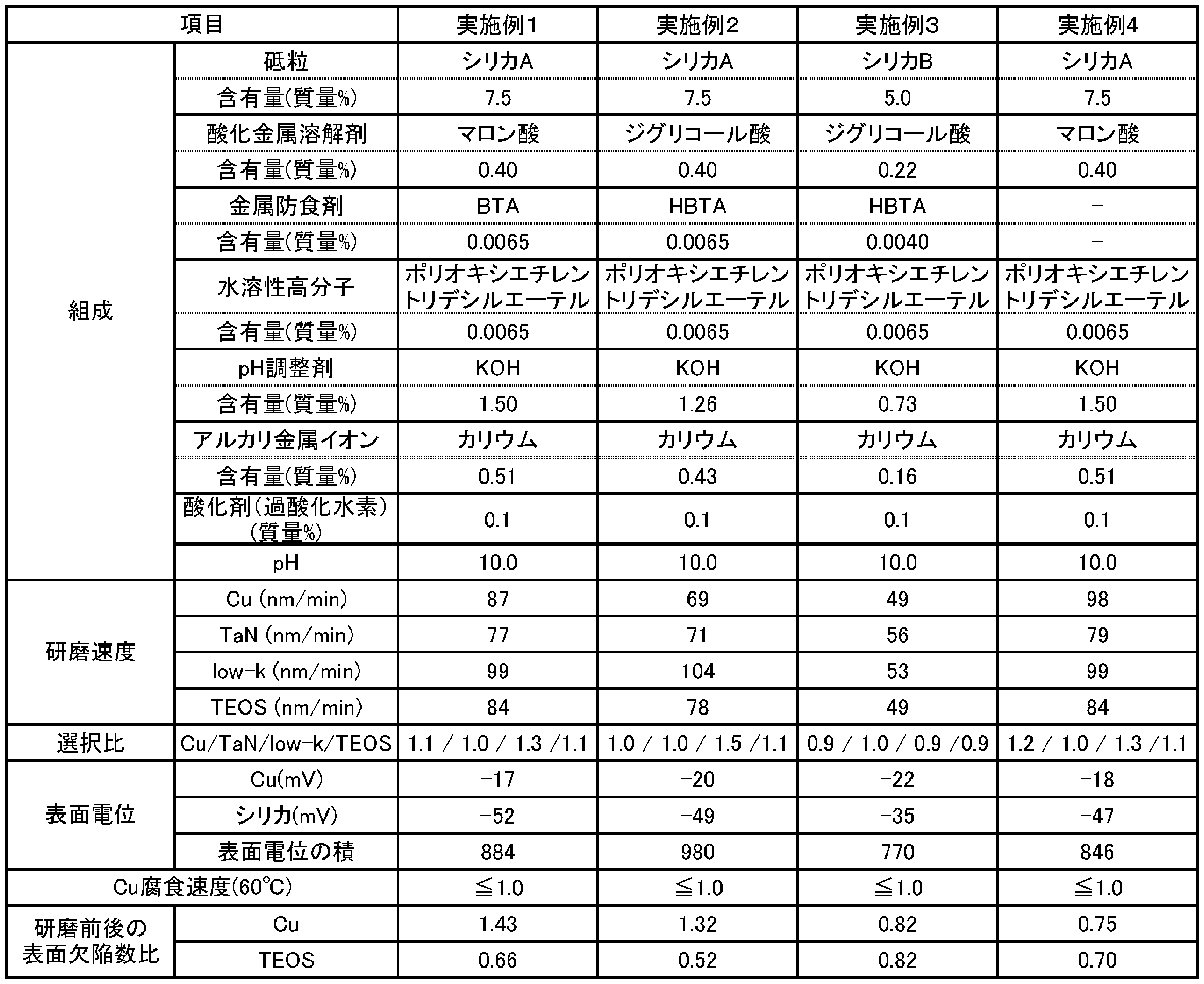
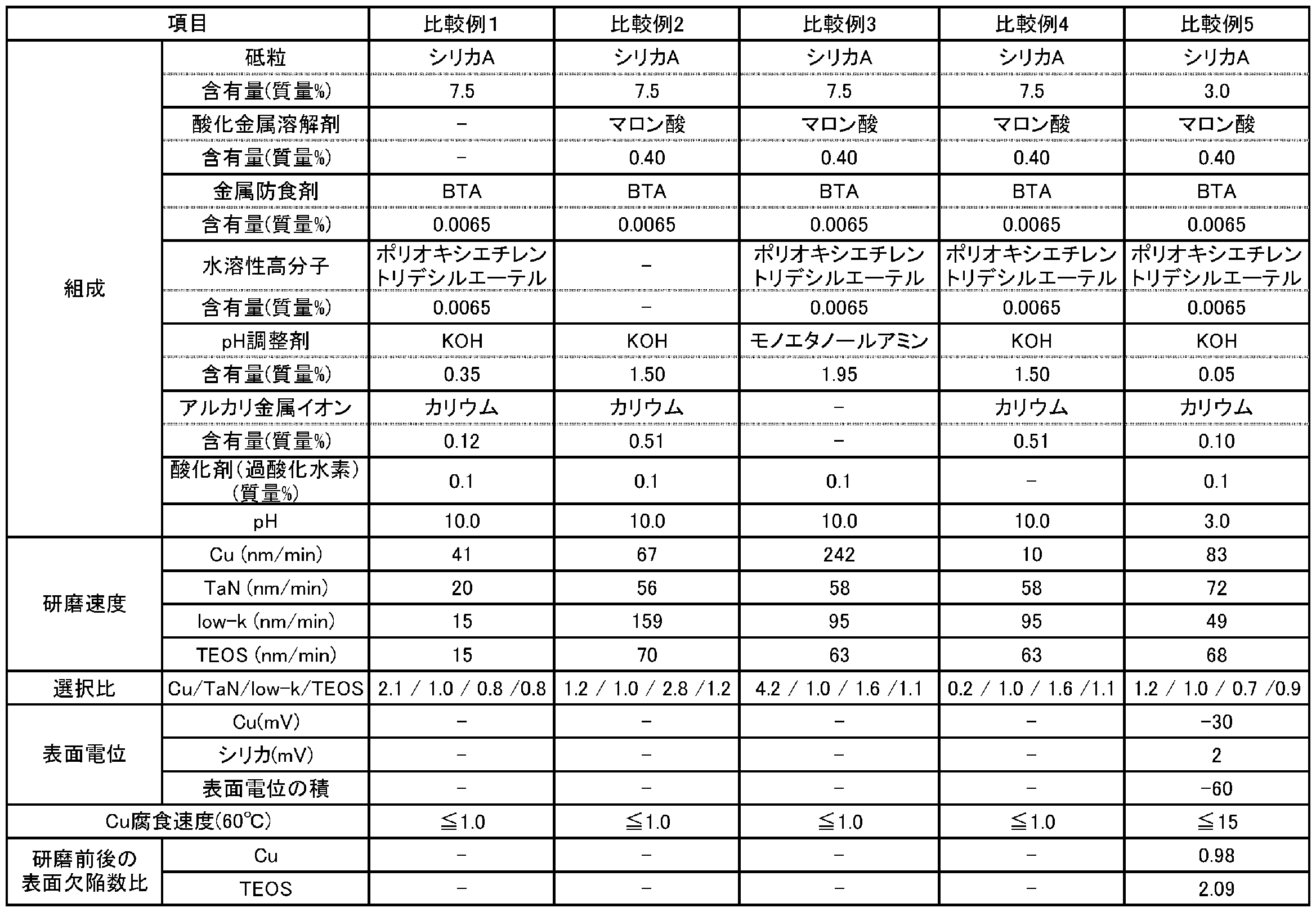
実施例1~4はTaN、TEOSの研磨速度が高く、またCuとlow-kの研磨速度もTaN、TEOSと同程度であり研磨速度および研磨速度の選択比ともに良好であった。またCuの腐食も無く、CuおよびTEOS表面の欠陥も低い値となっていた。一方、酸化金属溶解剤を加えなかった比較例1はTEOSとTaNの研磨速度が非常に低い値となった。また水溶性高分子を加えなかった比較例2はlow-kの研磨速度が159nm/minと非常に大きい値となった。また比較例3ではカリウムイオン源であるpH調整剤の水酸化カリウムを使用せず、モノエタノールアミンを使用しているが、Cuの研磨速度が著しく増加した。また比較例4では酸化剤を加えなかったが、Cuの研磨速度が著しく低い値となった。また比較例5では表面電位の積が負の値であるが、Cuに対する腐食速度が高く、さらにTEOS表面の欠陥数も高い値となった。
Claims (8)
- 少なくともバリアメタル、金属膜及び二酸化珪素膜を含む基板、又は少なくともバリアメタル、金属膜、二酸化珪素膜及びlow-k膜を含む基板を研磨するためのCMP用研磨液であって、
研磨粒子、酸化金属溶解剤、酸化剤、水溶性高分子及びアルカリ金属イオンを含有し、
研磨時における前記研磨粒子及び前記金属膜の表面電位が同符号であり、前記研磨粒子の表面電位(mV)と前記金属膜の表面電位(mV)との積が250~10000であり、
pHが7.0~11.0である、研磨液。 - 前記研磨粒子が会合粒子を形成しており、前記会合粒子の平均二次粒径が120nm以下である、請求項1に記載の研磨液。
- 前記研磨粒子の含有量が1~20質量%である、請求項1又は2に記載の研磨液。
- 前記研磨粒子がシリカ粒子を含む、請求項1~3のいずれか一項に記載の研磨液。
- 前記酸化金属溶解剤がクエン酸、マロン酸、ジグリコール酸、イソフタル酸及びメチルコハク酸からなる群より選択される少なくとも1種を含む、請求項1~4のいずれか一項に記載の研磨液。
- 前記水溶性高分子が下記一般式(1)の構造を有する、請求項1~5のいずれか一項に記載の研磨液。
RO-Xn-Ym-H (1)
[式中、Rは炭素数が6個以上のアルキル基、アルケニル基、フェニル基、多環フェニル基、アルキルフェニル基又はアルケニルフェニル基を示し、X及びYは、それぞれ側鎖に置換基を有していてもよいオキシエチレン基及びオキシプロピレン基を示す。またn及びmは、それぞれ0以上の整数を示し、n+mは4以上の整数である。] - 前記アルカリ金属イオンがカリウムイオンである、請求項1~6のいずれか一項に記載の研磨液。
- 研磨定盤の研磨布上に請求項1~7のいずれか一項に記載のCMP用研磨液を供給しながら、少なくともバリアメタル、金属膜及び二酸化珪素膜を含む基板、又は少なくともバリアメタル、金属膜、二酸化珪素膜及びlow-k膜を含む基板を前記研磨布に押圧した状態で前記研磨定盤と前記基板とを相対的に動かす工程を備える、研磨方法。
Priority Applications (5)
| Application Number | Priority Date | Filing Date | Title |
|---|---|---|---|
| KR1020187037654A KR20190017815A (ko) | 2016-06-09 | 2017-06-09 | Cmp용 연마액 및 연마 방법 |
| CN201780048056.6A CN109690741A (zh) | 2016-06-09 | 2017-06-09 | Cmp用研磨液和研磨方法 |
| US16/308,009 US20190256741A1 (en) | 2016-06-09 | 2017-06-09 | Cmp polishing solution and polishing method |
| JP2018521790A JPWO2017213255A1 (ja) | 2016-06-09 | 2017-06-09 | Cmp用研磨液及び研磨方法 |
| US17/197,991 US11359114B2 (en) | 2016-06-09 | 2021-03-10 | Polishing method using CMP polishing liquid |
Applications Claiming Priority (2)
| Application Number | Priority Date | Filing Date | Title |
|---|---|---|---|
| JP2016-115567 | 2016-06-09 | ||
| JP2016115567 | 2016-06-09 |
Related Child Applications (2)
| Application Number | Title | Priority Date | Filing Date |
|---|---|---|---|
| US16/308,009 A-371-Of-International US20190256741A1 (en) | 2016-06-09 | 2017-06-09 | Cmp polishing solution and polishing method |
| US17/197,991 Division US11359114B2 (en) | 2016-06-09 | 2021-03-10 | Polishing method using CMP polishing liquid |
Publications (1)
| Publication Number | Publication Date |
|---|---|
| WO2017213255A1 true WO2017213255A1 (ja) | 2017-12-14 |
Family
ID=60578628
Family Applications (1)
| Application Number | Title | Priority Date | Filing Date |
|---|---|---|---|
| PCT/JP2017/021482 Ceased WO2017213255A1 (ja) | 2016-06-09 | 2017-06-09 | Cmp用研磨液及び研磨方法 |
Country Status (6)
| Country | Link |
|---|---|
| US (2) | US20190256741A1 (ja) |
| JP (1) | JPWO2017213255A1 (ja) |
| KR (1) | KR20190017815A (ja) |
| CN (1) | CN109690741A (ja) |
| TW (1) | TW201742900A (ja) |
| WO (1) | WO2017213255A1 (ja) |
Cited By (2)
| Publication number | Priority date | Publication date | Assignee | Title |
|---|---|---|---|---|
| JP2019203088A (ja) * | 2018-05-24 | 2019-11-28 | 株式会社バイコウスキージャパン | 研磨砥粒、その製造方法、それを含む研磨スラリー及びそれを用いる研磨方法 |
| KR20200036790A (ko) * | 2018-09-28 | 2020-04-07 | 버슘머트리얼즈 유에스, 엘엘씨 | 배리어 슬러리 제거율 개선 |
Families Citing this family (2)
| Publication number | Priority date | Publication date | Assignee | Title |
|---|---|---|---|---|
| JPWO2020262628A1 (ja) * | 2019-06-27 | 2020-12-30 | ||
| JP7575878B2 (ja) * | 2020-03-24 | 2024-10-30 | 株式会社フジミインコーポレーテッド | 研磨用組成物、その製造方法、および研磨方法 |
Citations (5)
| Publication number | Priority date | Publication date | Assignee | Title |
|---|---|---|---|---|
| JP2003173990A (ja) * | 2001-12-07 | 2003-06-20 | Asahi Kasei Corp | 半導体基板の製造方法 |
| JP2007273621A (ja) * | 2006-03-30 | 2007-10-18 | Jsr Corp | 化学機械研磨用水系分散体および化学機械研磨方法 |
| JP2009272418A (ja) * | 2008-05-07 | 2009-11-19 | Asahi Glass Co Ltd | 研磨剤組成物および半導体集積回路装置の製造方法 |
| JP2010087338A (ja) * | 2008-10-01 | 2010-04-15 | Panasonic Corp | 半導体装置の製造方法および半導体製造装置 |
| JP2014069260A (ja) * | 2012-09-28 | 2014-04-21 | Fujimi Inc | 研磨用組成物 |
Family Cites Families (17)
| Publication number | Priority date | Publication date | Assignee | Title |
|---|---|---|---|---|
| US4944836A (en) | 1985-10-28 | 1990-07-31 | International Business Machines Corporation | Chem-mech polishing method for producing coplanar metal/insulator films on a substrate |
| US4954142A (en) | 1989-03-07 | 1990-09-04 | International Business Machines Corporation | Method of chemical-mechanical polishing an electronic component substrate and polishing slurry therefor |
| US6080802A (en) * | 1991-12-03 | 2000-06-27 | Rohm And Haas Company | Process for preparing an aqueous dispersion of composite particles including polymeric latex adsorbed to titanium dioxide |
| EP1036836B1 (en) * | 1999-03-18 | 2004-11-03 | Kabushiki Kaisha Toshiba | Aqueous dispersion for chemical mechanical polishing |
| TW501197B (en) | 1999-08-17 | 2002-09-01 | Hitachi Chemical Co Ltd | Polishing compound for chemical mechanical polishing and method for polishing substrate |
| US20030168627A1 (en) * | 2002-02-22 | 2003-09-11 | Singh Rajiv K. | Slurry and method for chemical mechanical polishing of metal structures including refractory metal based barrier layers |
| JP3892846B2 (ja) * | 2003-11-27 | 2007-03-14 | 株式会社東芝 | Cmp用スラリー、研磨方法、および半導体装置の製造方法 |
| US20070196975A1 (en) * | 2004-04-12 | 2007-08-23 | Hitachi Chemical Co., Ltd. | Metal-Polishing Liquid And Polishing Method Using The Same |
| JPWO2006030595A1 (ja) * | 2004-09-14 | 2008-05-08 | 日立化成工業株式会社 | Cmp用研磨スラリー |
| JPWO2007060869A1 (ja) * | 2005-11-24 | 2009-05-07 | Jsr株式会社 | 化学機械研磨用水系分散体および化学機械研磨方法 |
| JP4804986B2 (ja) * | 2006-03-30 | 2011-11-02 | 富士フイルム株式会社 | 半導体デバイス用基板の洗浄液及びそれを用いた洗浄方法 |
| JP2008181955A (ja) * | 2007-01-23 | 2008-08-07 | Fujifilm Corp | 金属用研磨液及びそれを用いた研磨方法 |
| JP2008277723A (ja) * | 2007-03-30 | 2008-11-13 | Fujifilm Corp | 金属用研磨液及び研磨方法 |
| TW200946621A (en) * | 2007-10-29 | 2009-11-16 | Ekc Technology Inc | Chemical mechanical polishing and wafer cleaning composition comprising amidoxime compounds and associated method for use |
| WO2009058275A1 (en) * | 2007-10-29 | 2009-05-07 | Ekc Technology, Inc. | Methods of post chemical mechanical polishing and wafer cleaning using amidoxime compositions |
| KR101563023B1 (ko) | 2008-02-18 | 2015-10-23 | 제이에스알 가부시끼가이샤 | 화학 기계 연마용 수계 분산체 및 화학 기계 연마 방법 |
| JP6797811B2 (ja) * | 2015-09-30 | 2020-12-09 | 株式会社フジミインコーポレーテッド | 研磨方法 |
-
2017
- 2017-06-09 KR KR1020187037654A patent/KR20190017815A/ko not_active Ceased
- 2017-06-09 CN CN201780048056.6A patent/CN109690741A/zh active Pending
- 2017-06-09 JP JP2018521790A patent/JPWO2017213255A1/ja active Pending
- 2017-06-09 WO PCT/JP2017/021482 patent/WO2017213255A1/ja not_active Ceased
- 2017-06-09 US US16/308,009 patent/US20190256741A1/en not_active Abandoned
- 2017-06-09 TW TW106119258A patent/TW201742900A/zh unknown
-
2021
- 2021-03-10 US US17/197,991 patent/US11359114B2/en active Active
Patent Citations (5)
| Publication number | Priority date | Publication date | Assignee | Title |
|---|---|---|---|---|
| JP2003173990A (ja) * | 2001-12-07 | 2003-06-20 | Asahi Kasei Corp | 半導体基板の製造方法 |
| JP2007273621A (ja) * | 2006-03-30 | 2007-10-18 | Jsr Corp | 化学機械研磨用水系分散体および化学機械研磨方法 |
| JP2009272418A (ja) * | 2008-05-07 | 2009-11-19 | Asahi Glass Co Ltd | 研磨剤組成物および半導体集積回路装置の製造方法 |
| JP2010087338A (ja) * | 2008-10-01 | 2010-04-15 | Panasonic Corp | 半導体装置の製造方法および半導体製造装置 |
| JP2014069260A (ja) * | 2012-09-28 | 2014-04-21 | Fujimi Inc | 研磨用組成物 |
Cited By (7)
| Publication number | Priority date | Publication date | Assignee | Title |
|---|---|---|---|---|
| JP2019203088A (ja) * | 2018-05-24 | 2019-11-28 | 株式会社バイコウスキージャパン | 研磨砥粒、その製造方法、それを含む研磨スラリー及びそれを用いる研磨方法 |
| JP7220522B2 (ja) | 2018-05-24 | 2023-02-10 | 株式会社バイコウスキージャパン | 研磨砥粒、その製造方法、それを含む研磨スラリー及びそれを用いる研磨方法 |
| KR20200036790A (ko) * | 2018-09-28 | 2020-04-07 | 버슘머트리얼즈 유에스, 엘엘씨 | 배리어 슬러리 제거율 개선 |
| JP2020059847A (ja) * | 2018-09-28 | 2020-04-16 | バーサム マテリアルズ ユーエス,リミティド ライアビリティ カンパニー | バリアスラリー除去速度の改善 |
| CN111087929A (zh) * | 2018-09-28 | 2020-05-01 | 弗萨姆材料美国有限责任公司 | 屏障浆料去除速率改善 |
| JP7048550B2 (ja) | 2018-09-28 | 2022-04-05 | バーサム マテリアルズ ユーエス,リミティド ライアビリティ カンパニー | バリアスラリー除去速度の改善 |
| KR102406821B1 (ko) | 2018-09-28 | 2022-06-10 | 버슘머트리얼즈 유에스, 엘엘씨 | 배리어 슬러리 제거율 개선 |
Also Published As
| Publication number | Publication date |
|---|---|
| KR20190017815A (ko) | 2019-02-20 |
| JPWO2017213255A1 (ja) | 2019-05-16 |
| US20210189179A1 (en) | 2021-06-24 |
| US20190256741A1 (en) | 2019-08-22 |
| CN109690741A (zh) | 2019-04-26 |
| US11359114B2 (en) | 2022-06-14 |
| TW201742900A (zh) | 2017-12-16 |
Similar Documents
| Publication | Publication Date | Title |
|---|---|---|
| JP4853494B2 (ja) | 研磨液及び研磨方法 | |
| US8821750B2 (en) | Metal polishing slurry and polishing method | |
| JP4568604B2 (ja) | 研磨液及び研磨方法 | |
| CN104170065B (zh) | 研磨方法 | |
| US11359114B2 (en) | Polishing method using CMP polishing liquid | |
| JP5493526B2 (ja) | Cmp用研磨液及び研磨方法 | |
| TW201336977A (zh) | 用於鈷應用之漿料 | |
| WO2014175397A1 (ja) | Cmp用研磨液及びこれを用いた研磨方法 | |
| WO2014175393A1 (ja) | Cmp用研磨液及びこれを用いた研磨方法 | |
| JP2009278061A (ja) | Cmp用研磨液及び研磨方法 | |
| JP2016030778A (ja) | Cmp用研磨液及びこれを用いた研磨方法 | |
| JP2012134358A (ja) | Cmp研磨液及び研磨方法 | |
| JP2009124092A (ja) | タングステン用cmp研磨液および基板の研磨方法 | |
| JP2011014552A (ja) | 基板の研磨方法 | |
| JP2010114402A (ja) | Cmp用研磨液及びこのcmp用研磨液を用いた研磨方法 |
Legal Events
| Date | Code | Title | Description |
|---|---|---|---|
| ENP | Entry into the national phase |
Ref document number: 2018521790 Country of ref document: JP Kind code of ref document: A |
|
| 121 | Ep: the epo has been informed by wipo that ep was designated in this application |
Ref document number: 17810427 Country of ref document: EP Kind code of ref document: A1 |
|
| NENP | Non-entry into the national phase |
Ref country code: DE |
|
| ENP | Entry into the national phase |
Ref document number: 20187037654 Country of ref document: KR Kind code of ref document: A |
|
| 122 | Ep: pct application non-entry in european phase |
Ref document number: 17810427 Country of ref document: EP Kind code of ref document: A1 |