WO2017208307A1 - パワーアンプの保護回路、パワーアンプ、およびスピーカーユニット - Google Patents
パワーアンプの保護回路、パワーアンプ、およびスピーカーユニット Download PDFInfo
- Publication number
- WO2017208307A1 WO2017208307A1 PCT/JP2016/065919 JP2016065919W WO2017208307A1 WO 2017208307 A1 WO2017208307 A1 WO 2017208307A1 JP 2016065919 W JP2016065919 W JP 2016065919W WO 2017208307 A1 WO2017208307 A1 WO 2017208307A1
- Authority
- WO
- WIPO (PCT)
- Prior art keywords
- node
- transistor
- resistor
- protection
- circuit
- Prior art date
- Legal status (The legal status is an assumption and is not a legal conclusion. Google has not performed a legal analysis and makes no representation as to the accuracy of the status listed.)
- Ceased
Links
Images






Classifications
-
- H—ELECTRICITY
- H03—ELECTRONIC CIRCUITRY
- H03F—AMPLIFIERS
- H03F1/00—Details of amplifiers with only discharge tubes, only semiconductor devices or only unspecified devices as amplifying elements
- H03F1/52—Circuit arrangements for protecting such amplifiers
-
- H—ELECTRICITY
- H03—ELECTRONIC CIRCUITRY
- H03F—AMPLIFIERS
- H03F3/00—Amplifiers with only discharge tubes or only semiconductor devices as amplifying elements
- H03F3/26—Push-pull amplifiers; Phase-splitters therefor
-
- H—ELECTRICITY
- H04—ELECTRIC COMMUNICATION TECHNIQUE
- H04R—LOUDSPEAKERS, MICROPHONES, GRAMOPHONE PICK-UPS OR LIKE ACOUSTIC ELECTROMECHANICAL TRANSDUCERS; ELECTRIC HEARING AIDS; PUBLIC ADDRESS SYSTEMS
- H04R3/00—Circuits for transducers
Definitions
- the present invention relates to a technology for a power amplifier protection circuit, a power amplifier, and a speaker unit.
- Patent Document 1 As a power amplifier protection circuit, for example, a circuit as disclosed in Patent Document 1 is known. This circuit detects the voltage across the emitter resistance of the push-pull output stage and provides a transistor whose impedance changes according to the voltage across the terminal between the base of the transistor in the push-pull output stage and the amplifier output. is there. In this circuit, the drive capability of the push-pull output stage is limited according to the load, and the amplitude of the current flowing through the output terminal is suppressed, thereby suppressing the heat generation of the transistor in the push-pull output stage.
- a circuit as disclosed in Patent Document 2 is known.
- the current of the output stage of the amplifier circuit is detected by a microcomputer. If the microcomputer determines that an overcurrent has occurred, the microcomputer controls the protection circuit to operate. For example, the protection circuit operates by turning off the gate circuit to cut off the signal input to the drive circuit, turning off the output relay to cut off the audio signal output to the speaker, For example, the power output can be shut off.
- the present invention has been made in view of the above-described circumstances, and its purpose is to reliably detect abnormalities such as excessive input, overload, or deterioration of heat dissipation conditions without using a microcomputer, and in a power amplifier circuit. It is an object of the present invention to provide a power amplifier protection circuit, a power amplifier, and a speaker unit that can prevent destruction of elements.
- a power amplifier protection circuit includes a first node and a second node to which a signal is supplied, and a bias that applies a bias voltage to the first node and the second node.
- a circuit, a plurality of Darlington-connected transistors connected to the first node and the base and used to output a current from an output terminal, and a second node connected to the base and a current drawn from the output terminal A push-pull output circuit having a plurality of Darlington-connected transistors used, the first protection transistor having an emitter connected to the first node, and the first protection A first diode connected between a collector of a transistor and the output terminal; and the second node.
- a second protection transistor having an emitter connected to the second protection transistor; a second diode connected between a collector of the second protection transistor and the output terminal; and a second diode connected between the first node and the second node.
- a compressed voltage is applied to the base of the second protection transistor, and a voltage divided by the second resistor and the third resistor is applied to the base of the first protection transistor.
- the base current flows to the base of the second protection transistor, and the second protection transistor shifts to the active state.
- the collector current starts to flow, and the voltage between the first node and the second node starts to decrease. In this state, a negative feedback is applied to the second protection transistor and an analog operation is performed.
- the second protection transistor is completely turned on. As a result, the collector-emitter voltage of the second protection transistor is about 0V. Therefore, the voltage between the output terminal and the second node is equal to the forward voltage of the second diode.
- the voltage between the base and the emitter of the Darlington-connected transistor used for sucking current from the output terminal is smaller than the voltage necessary for turning on the Darlington-connected transistor.
- the Darlington-connected transistor is turned off.
- the collector-emitter voltage of the second protection transistor becomes about 0 V
- the first protection transistor is turned on via the second resistance and the third resistance.
- the collector-emitter voltage of the first protection transistor becomes about 0V. Therefore, the voltage between the output terminal and the first node is equal to the forward voltage of the first diode.
- the voltage between the base and the emitter of the plurality of Darlington-connected transistors used for outputting current from the output terminal is smaller than the voltage required to turn on the plurality of Darlington-connected transistors.
- the plurality of transistors connected in Darlington are turned off.
- the resistance value of the thermistor changes, and the operation of a plurality of Darlington-connected transistors of the push-pull output circuit can be stopped. Therefore, a plurality of Darlington-connected transistors of the push-pull output circuit can be widely protected regardless of the cause of abnormality, such as when the heat dissipating fan is stopped or the heat dissipating hole is blocked.
- the present invention when the set temperature is exceeded, a plurality of Darlington-connected transistors of the push-pull output circuit are completely stopped, so that heat generation can be completely stopped. Furthermore, since advanced signal processing by a microcomputer or the like is unnecessary, manufacturing cost can be reduced and the application range of the protection circuit can be expanded.
- the semiconductor device may further include a fourth resistor connected between the collector of the first protection transistor and the base of the second protection transistor.
- a fourth resistor connected between the collector of the first protection transistor and the base of the second protection transistor.
- the second protection transistor and the first protection transistor can be turned off when the temperature value drops to a desired temperature and the resistance value of the thermistor changes.
- a fifth resistor connected between a connection node of the first resistor and the thermistor and a base of the second protection transistor may be further provided.
- the fifth resistor by providing the fifth resistor, the second protection transistor can be kept on even when the temperature is lowered and the resistance value of the thermistor is changed.
- the protection transistor can be left on. Therefore, after the protection circuit is turned on once, a latch operation can be realized in which the protection circuit remains on even when the temperature returns to room temperature, and a safer operation is realized as compared with the case where the fifth resistor is not provided.
- the current control for applying a predetermined voltage to the base of the second protection transistor so that the second protection transistor is turned on when detecting that the amplitude of the current flowing through the output terminal exceeds a predetermined level.
- a circuit may be provided. According to this aspect, when an excessive current flows through the load, a predetermined voltage is applied to the base of the second protection transistor by the current control circuit, and the second protection transistor is turned on. Therefore, the protection circuit is turned on, and the driving of the plurality of transistors connected to the Darlington of the push-pull output circuit is stopped. As a result, even when the element is destroyed, the short-circuit current from the positive power supply voltage to the negative power supply voltage does not flow continuously, and subsequent damage expansion can be prevented.
- the first protection transistor and the second protection transistor are turned on to drive the plurality of Darlington-connected push-pull output circuits. Stop. Therefore, it is possible to protect the power amplifier against temperature rise.
- the current control circuit is turned on when the amplitude of the current flowing through the output terminal exceeds a predetermined level
- the current detection circuit includes a current detection transistor that supplies a positive power supply voltage to a collector; and the current detection circuit A third diode and a sixth resistor connected between the collector of the transistor and the base of the second protection transistor may be provided.
- the current detection transistor when an excessive current flows through the load, the current detection transistor is turned on, and a predetermined voltage is applied to the base of the second protection transistor via the third diode and the sixth resistor, so that the second protection The transistor turns on. Further, when the second protection transistor is turned on, the first protection transistor is turned on.
- the first protection transistor and the second protection transistor are turned on, the driving of the Darlington-connected transistor of the push-pull output circuit is stopped. As a result, even when the element is destroyed, the short-circuit current from the positive power supply voltage to the negative power supply voltage does not flow continuously, and subsequent damage expansion can be prevented. Further, according to this aspect, even when the temperature of the power amplifier rises above the set temperature, the first protection transistor and the second protection transistor are turned on to stop the drive of the Darlington-connected transistor of the push-pull output circuit. . Therefore, it is possible to protect the power amplifier against temperature rise.
- the thermistor may be a positive temperature coefficient thermistor in which one terminal is connected to the second node and the other terminal is connected to the first resistor.
- the positive temperature coefficient thermistor has a characteristic in which the resistance value suddenly changes with respect to a specific temperature
- the negative temperature coefficient thermistor is used as the first protection transistor and the second protection transistor. It can be operated more digitally than the case. Therefore, the power amplifier can be reliably protected.
- the thermistor may be a negative characteristic thermistor in which one terminal is connected to the first node and the other terminal is connected to the first resistor.
- the change in resistance value of the negative characteristic thermistor is generally not as steep as compared to the positive characteristic thermistor.
- the first protection transistor and the second protection transistor are operated digitally if a certain value is exceeded even if the resistance change with respect to temperature is moderate. Can be made.
- a power amplifier protection circuit includes a first node and a second node to which a signal is supplied, and a bias that applies a bias voltage to the first node and the second node.
- a current detection circuit including a current detection transistor supplied to a collector;
- a third protection transistor having an emitter connected to the output terminal and a fourth diode and a seventh resistor connected between a collector of the current detection transistor and a base of the third protection transistor;
- An eighth resistor connected between the base of the third protection transistor and
- the current detection transistor when an excessive current flows to the output terminal, the current detection transistor is turned on, and a base current flows to the base of the third protection transistor via the fourth diode and the seventh resistor, so that the third protection The transistor turns on. Therefore, the first node and the output terminal are short-circuited, and in the push-pull output circuit, the first node and the base are connected and the transistor used for outputting current from the output terminal is turned off.
- the current detection transistor is turned on
- the fifth protection transistor is turned on.
- the fourth protection transistor is turned on via the fifth diode and the ninth resistor.
- the second node and the output terminal are short-circuited, and in the push-pull output circuit, the second node and the base are connected and the transistor used to suck current from the output terminal is turned off.
- the fifth protection transistor is turned on, positive feedback is applied to the current detection transistor via the twelfth resistor.
- the current detection transistor can be kept on. Also, when the temperature of the power amplifier rises and the resistance value of the thermistor changes to a predetermined value, the current detection transistor is turned on via the sixth diode.
- the transistor used to suck in turns off.
- the transistor of the push-pull output circuit is turned off when an overcurrent flows through the load and when the temperature of the power amplifier rises above the set temperature. Therefore, the power amplifier can be protected regardless of the cause of the abnormality, and the protection can be continued.
- the present invention can be conceptualized as a power amplifier protection circuit, a power amplifier having the power amplifier protection circuit, and a speaker unit having the power amplifier.
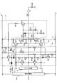
- FIG. 1 is a circuit diagram showing an output circuit and a protection circuit of a power amplifier according to a first embodiment of the present invention. It is a circuit diagram which shows the output circuit and protection circuit of a power amplifier which concern on 2nd Embodiment of this invention. It is a figure which shows the relationship between the detection temperature by the thermistor in 1st Embodiment, and ON / OFF of a protection circuit. It is a figure which shows the relationship between the detection temperature by the thermistor in 2nd Embodiment, and ON / OFF of a protection circuit. It is a circuit diagram which shows the output circuit and protection circuit of a power amplifier which concern on 3rd Embodiment of this invention.
- FIG. 10 is a circuit diagram showing an output circuit and a protection circuit of a power amplifier according to Modification 1.
- FIG. 10 is a circuit diagram showing an output circuit and a protection circuit of a power amplifier according to Modification 2.
- FIG. 10 is a circuit diagram showing an output circuit and a protection circuit of a power amplifier according to Modification 2.
- FIG. 10 is a circuit diagram showing an output circuit and a protection circuit of a power amplifier according to Modification 3.
- FIG. 10 is a circuit diagram showing an output circuit and a protection circuit of a power amplifier according to Modification 4. It is a block diagram which shows the speaker unit which concerns on an application example. It is a perspective view which shows the speaker unit which concerns on an application example. It is a perspective view which shows the speaker unit which concerns on an application example. It is a perspective view which shows the speaker unit which concerns on an application example. It is a perspective view which shows the speaker unit which concerns on an application example.
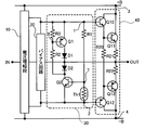
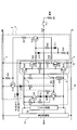
- FIG. 1 is a circuit diagram showing an output circuit of a power amplifier and a protection circuit of the power amplifier according to the first embodiment.
- the output circuit of the power amplifier includes a voltage amplification stage 10, a bias circuit 20, and a SEPP circuit 40.
- An SEPP (Single Ended Push-Pull, single-ended push-pull) circuit 40 as a push-pull output circuit includes transistors Q10, Q11, Q12, and Q13, and resistors R20, R21, and R22.
- the NPN transistor Q10 and the NPN transistor Q11 are Darlington-connected transistors.
- the base of the NPN transistor Q10 is connected to the first node 1 to which a signal is supplied, and is connected to the NPN transistor Q11 by Darlington.
- the transistor Q10 and the transistor Q11 are transistors used to output current from the output terminal OUT.
- the collectors of the transistors Q10 and Q11 are connected to the third node 3 to which the positive power supply voltage + B is supplied.
- the PNP transistor Q12 and the PNP transistor Q13 are Darlington-connected transistors.
- the base of the PNP transistor Q12 is connected to the second node 2 to which a signal is supplied, and is connected to the PNP transistor Q13 by Darlington.
- the transistors Q12 and Q13 are transistors used for sucking current from the output terminal OUT.
- the collectors of the transistors Q12 and Q13 are connected to the fourth node 4 to which the negative power supply voltage -B is supplied.
- the voltage amplification stage 10 is connected to the third node 3 and the fourth node 4, and supplies a signal obtained by amplifying an input signal to a predetermined voltage from the input terminal IN to the first node 1 and the second node 2.
- the bias circuit 20 is connected to the first node 1 and the second node 2 and applies a predetermined bias voltage to the first node 1 and the second node 2. As a result, crossover distortion in the SEPP circuit 40 is reduced.
- the first protection circuit 30 as a power amplifier protection circuit includes a PNP-type first protection transistor Q1 and an NPN-type second protection transistor Q2.
- the emitter of the first protection transistor Q1 is connected to the first node 1.
- the emitter of the second protection transistor Q2 is connected to the second node 2.
- a first diode D1 is connected between the collector of the first protection transistor Q1 and the output terminal OUT.
- a second diode D2 is connected between the collector of the second protection transistor Q2 and the output terminal OUT.
- the first diode D1 and the second diode D2 are connected as described above. These diodes hold the voltage between the first node 1 and the second node 2 at about 1.2 V when the first protection transistor Q1 and the second protection transistor Q2 are turned on.
- the first resistor R1 and the thermistor Th1 are connected in series between the first node 1 and the second node 2.
- a connection node 7 between the first resistor R1 and the thermistor Th1 is connected to the base of the second protection transistor Q2, and a predetermined voltage divided by the first resistor R1 and the thermistor Th1 is applied to the second protection transistor Q2. Applied to the base.
- the first resistor R1 and the thermistor Th1 are used to turn on the second protection transistor Q2 when the temperature of the power amplifier detected by the thermistor Th1 reaches a predetermined temperature.
- the thermistor Th1 is a positive temperature coefficient thermistor whose resistance value increases as the temperature increases.
- a second resistor R2 and a third resistor R3 are connected in series between the first node 1 and the collector of the second protection transistor Q2.
- a connection node 8 between the second resistor R2 and the third resistor R3 is connected to the base of the first protection transistor Q1, and a predetermined voltage divided by the second resistor R2 and the third resistor R3 is applied to the first protection transistor Q1. Applied to the base.
- the second resistor R2 and the third resistor R3 are used to turn on the first protection transistor Q1 when the second protection transistor Q2 is turned on.
- a transistor being in an active state means that the transistor operates in an active region.
- a transistor When a transistor is turned on, it means that the transistor operates in a saturation region.
- the transistor When the transistor is turned off, it means that the transistor operates in the cutoff region.
- the first protection circuit 30 is set to operate at 100 ° C.
- the resistance value of the thermistor Th1 is 10 K ⁇ at 100 ° C.
- the voltage across the bias circuit 20, that is, the voltage between the first node 1 and the second node 2 is the base-emitter voltage Vbe when the transistors Q11 and Q13 of the SEPP circuit 40 become active.
- the voltage between the first node 1 and the second node 2 is about 2.4V.
- the voltage generated by the voltage division between the first resistor R1 and the thermistor Th1 may be about 0.6V or more. Therefore, the following formula is established.
- the equation for obtaining the resistance value of the first resistor R1 is as follows.
- Resistance value of the first resistor R1 (2.4 [V] ⁇ (resistance value of the thermistor Th1) /0.6 [V] ⁇ (resistance value of the thermistor Th1) ... Equation 2
- the resistance value of the first resistor R1 is as follows.
- the resistance value of the thermistor Th1 changes when the temperature changes from room temperature to 100 ° C., and current starts to flow to the base of the second protection transistor Q2.
- the second protection transistor Q2 shifts to an active state.
- the second protection transistor Q2 becomes active, the collector current starts to flow, and the voltage between the first node 1 and the second node 2 starts to drop.
- negative feedback is applied to the second protection transistor Q2 to perform an analog operation, but in this state, negative feedback is applied to the second protection transistor Q2 to perform an analog operation, but the temperature rises further and the thermistor Th1.
- the resistance value of the second protection transistor Q2 increases, the second protection transistor Q2 is completely turned on.
- the collector-emitter voltage Vce of the second protection transistor Q2 is about 0V.
- the voltage between the output terminal OUT and the second node 2 becomes approximately 0.6 V, which is the forward voltage of the second diode D2.
- the voltage between the base of the transistor Q12 connected to the second node 2 and the emitter of the transistor Q13 connected to the output terminal OUT via the resistor R22 is also about 0.6V.
- This voltage of about 0.6 V is more than about 1.2 V, which is the sum of the base-emitter voltage Vbe when the transistor Q12 becomes active and the base-emitter voltage Vbe when the transistor Q13 becomes active. small. Therefore, the transistor Q12 and the transistor Q13 are turned off.
- the first protection transistor Q1 is turned on via the second resistor R2 and the third resistor R3.
- the collector-emitter voltage Vce of the first protection transistor Q1 becomes about 0V.
- the voltage between the output terminal OUT and the first node 1 becomes about 0.6 V which is the forward voltage of the first diode D1.
- the voltage between the base of the transistor Q10 connected to the first node 2 and the emitter of the transistor Q11 connected to the output terminal OUT via the resistor R21 is also about 0.6V.
- This voltage of about 0.6 V is more than about 1.2 V, which is the sum of the base-emitter voltage Vbe when the transistor Q10 becomes active and the base-emitter voltage Vbe when the transistor Q11 becomes active. small. Therefore, the transistor Q10 and the transistor Q11 are turned off. Note that the resistance values of the second resistor R2 and the third resistor R3 can be freely selected within a range in which the first protection transistor Q1 can be turned on and other circuit operations are not adversely affected.
- the SEPP circuit 40 when the temperature of the power amplifier exceeds the set temperature and the resistance value of the thermistor Th1 changes and becomes a predetermined value, the SEPP circuit 40 The operation of the output stage transistor can be stopped. Therefore, the transistors in the output stage of the SEPP circuit 40 can be widely protected regardless of the cause of abnormality, such as when the heat dissipating fan is stopped or the heat dissipating hole is blocked. Further, according to the first protection circuit 30 of the present embodiment, when the set temperature is exceeded, the transistor at the output stage of the SEPP circuit 40 is completely stopped, so that heat generation can be completely stopped. Furthermore, since advanced signal processing by a microcomputer or the like is not necessary, the manufacturing cost can be reduced and the application range of the first protection circuit 30 can be expanded.
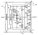
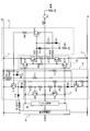
- FIG. 2 is a circuit diagram showing the first protection circuit 30 of the power amplifier according to the second embodiment.
- a fourth resistor R4 is connected between the collector of the first protection transistor Q1 and the base of the second protection transistor Q2.
- the collectors and emitters of the first protection transistor Q1 and the second protection transistor Q2 The voltage between is about 0V.
- the voltage between the first node 1 and the second node 2 depends on the forward voltage of the first diode D1 and the second diode D2, and is about 1.2V.
- the voltage generated by the voltage division between the first resistor R1 and the thermistor Th1 may be about 0.6V or more. Therefore, the following formula is established.
- the equation for obtaining the resistance value of the thermistor Th1 is as follows.
- Resistance value of thermistor Th1 (0.6 [V] ⁇ (resistance value of the first resistor R1)) / 0.6
- the resistance value of the first resistor R1 is 30 [K ⁇ ]
- the resistance value of the thermistor Th1 at this time is as follows.
- the second protection transistor Q2 is not completely turned on.
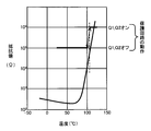
- the resistance value of the thermistor Th1 is 30 [K ⁇ ] as shown in FIG. 3 at a temperature slightly higher than 100 ° C., for example, around 105 ° C. Therefore, until the temperature reaches 105 ° C., the first protection circuit 30 of the first embodiment is operating in an analog manner.
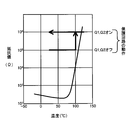
- the fourth resistor R4 since the fourth resistor R4 is provided, when the first protection transistor Q1 starts to shift to the active state, the base current is supplied to the base of the second protection transistor Q2 via the fourth resistor R4. Flows. Therefore, even if the resistance value of the thermistor Th1 near 100 ° C. at which the second protection transistor Q2 becomes active is 10 [K ⁇ ], the base current from the fourth resistor R4 is added, and as shown in FIG. 2 The protection transistor Q2 can be completely turned on.
- the parallel resistance value of the first resistor R1 and the fourth resistor R4 can be obtained by the following equation.
- the parallel resistance value of the first resistor R1 and the fourth resistor R4 1.2 [V] ⁇ (resistance value of the thermistor Th1) /0.6V [V] ⁇ (resistance value of the thermistor Th1).
- the parallel resistance values of the first resistor R1 and the fourth resistor R4 are as follows.
- the fourth resistor R4 is 15 [K ⁇ ]. Therefore, by using a resistor of 15 [K ⁇ ] or less as the fourth resistor R4, the first protection transistor Q1 and the second protection transistor Q2 are completely at the temperature at which the first protection transistor Q1 starts to enter the active state. And can be turned on.
- the base of the second protection transistor Q2 is around 105 ° C to 100 ° C by performing an analog operation similar to that when the temperature is lowered when the temperature is lowered. Current stops flowing. As a result, the first protection transistor Q1 and the second protection transistor Q2 of the first protection circuit 30 are turned off.
- the presence of the fourth resistor R4 is equivalent to the case where the first resistor R1 and the fourth resistor R4 are connected in parallel when the first protection transistor Q1 is on. Accordingly, the second protection transistor Q2 of the first protection circuit 30 is not turned off unless the temperature is lower than the temperature around 105 ° C. to 100 ° C.
- the parallel resistance values of the first resistor R1 and the fourth resistor R4 are as follows: Become. The resistance value of the thermistor Th1 of the equation 2 is set to 1 K ⁇ , and the “resistance value of the first resistor R1” in the equation 2 is replaced with “the resistance value of the first resistor R1 and the fourth resistor R4 in parallel”.
- the fourth resistor R4 is 3.3 [K ⁇ ].
- the second protection transistor Q2 of the first protection circuit 30 can be turned off when the temperature falls below 100 ° C. .
- the first protection transistor Q1 and the second protection transistor Q2 are not simultaneously turned on / off within the range, and the operation of the first protection circuit 30 with respect to the temperature on the plus side and the minus side can be prevented from being different. it can.
- inconveniences such as frequent on / off of the first protection transistor Q1 and the second protection transistor Q2 of the first protection circuit 30 due to a subtle change in temperature are eliminated.
- FIG. 5 is a circuit diagram showing the first protection circuit 30 of the power amplifier according to the third embodiment.
- a fifth resistor R5 connected between the connection node 7 between the first resistor R1 and the thermistor Th1 and the base of the second protection transistor Q2 is further provided.
- the fourth resistor R4 is added, and a hysteresis operation is added between on and off of the first protection circuit 30.
- the fifth resistor R5 as shown in FIG. 5, after the first protection circuit 30 is once turned on, the first protection circuit 30 is kept on even when the temperature returns to room temperature. Can do.
- the first resistance R1 is 30 [K ⁇ ] and the operation start temperature of the first protection circuit 30 is around 100 ° C.
- the first protection transistor Q1 and the second protection transistor Q2 continue to be turned on even when the temperature decreases and the resistance value of the thermistor Th1 approaches 0 ⁇ .
- the resistance values of the fourth resistor R4 and the fifth resistor R5 are set. Assuming that the connector-emitter voltage of the first protection transistor Q1 is 0V and the thermistor Th1 is 0 ⁇ , the relationship between the fourth resistor R4 and the fifth resistor R5 is the same as that of the first resistor R1 described in the second embodiment. It is the same as the relationship of Mr. Th1. Further, since it is assumed that the first protection transistor Q1 and the second protection transistor Q2 are turned on, the voltage between the first node 1 and the second node 2 is about 1.2V.
- the resistance value of the fourth resistor R4 is set to 3.3 K ⁇ as described in the second embodiment.
- the resistance value of the fifth resistor R5 can be obtained by the following equation.
- the resistance value of the fifth resistor R5 is set to 3.3 K ⁇ or more, even if the temperature decreases and the thermistor Th1 becomes a low resistance value as shown in FIG.
- the first protection transistor Q1 and the second protection transistor Q2 are kept on.
- the protection state of the transistor in the output stage of the SEPP circuit 40 is maintained.
- the power supply may be once cut off.
- the present embodiment by adding the fifth resistor R5, after the first protection transistor Q1 and the second protection transistor Q2 are once turned on, the first protection transistor Q1 and the second protection transistor Q2 Latch operation can be realized while the signal is on. As a result, the protection operation of the transistors in the output stage of the SEPP circuit 40 by the first protection circuit 30 is continued until the user turns off the power, and a safer operation is realized as compared with the second embodiment.
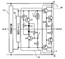
- FIG. 7 is a circuit diagram illustrating a power amplifier protection circuit according to the fourth embodiment.
- the power amplifier protection circuit of the present embodiment includes a first protection circuit 30 and a current control circuit 5.
- the relay RL1 is provided at the subsequent stage of the output terminal OUT, and the relay RL1 is turned off by the operation of the current control circuit 5.
- the function of detecting the temperature and protecting the power amplifier is realized. Therefore, for example, when the current increases due to excessive input or the like and the temperature rises, the protection operation by the first protection circuit 30 can be performed.
- the current control circuit 5 is incorporated in the circuit of the third embodiment, and the protection operation of the power amplifier is performed.
- the current control circuit 5 of the present embodiment detects that the amplitude of the current flowing through the output terminal OUT has exceeded a predetermined level, a predetermined value is applied to the base of the second protection transistor Q2 so that the second protection transistor Q2 is turned on.
- the current control circuit 5 of this embodiment includes a current detection circuit 6, a third diode D3, and a sixth resistor R6.
- the current detection circuit 6 includes resistors R23, R24, R25, R26, R27, and R28, diodes D10, D11, and D12, a first current detection transistor Q14, and a second current detection transistor Q15.
- the first current detection transistor Q14 When the amplitude of the current flowing through the output terminal OUT exceeds a predetermined level, the first current detection transistor Q14 is turned on, the second current detection transistor Q15 is turned on, and the positive power supply voltage + B is applied to the collector of the second current detection transistor Q15. Supplied.
- a third diode D3 and a sixth resistor R6 are connected between the collector of the second current detection transistor Q15 and the base of the second protection transistor Q2.
- the first current detection transistor Q14 when an excessive current flows through the output terminal OUT, the first current detection transistor Q14 is turned on, and further the second current detection transistor Q15 is turned on. As a result, a base current flows to the base of the second protection transistor Q2 via the third diode D3 and the sixth resistor R6, and the second protection transistor Q2 is turned on.
- the subsequent operation is the same as that of the above-described embodiment, and the first protection circuit 30 can continuously limit the drive capability of the output stage of the SEPP circuit 40.
- the power amplifier can be protected by turning off the relay RL1.
- a transistor eg, Q11
- the transistor for example, Q13
- the transistor on the other side of the output stage of the SEPP circuit 40 is also destroyed, and the risk of fire or the like may increase.
- the transistor on one side of the output stage of the SEPP circuit 40 is broken and an excessive current flows, not only the relay RL1 is turned off but also the first protection circuit 30 is turned on and the SEPP circuit 40 The driving of the transistor on the other side of the output stage is stopped. Therefore, the short-circuit current from the positive power supply voltage + B to the negative power supply voltage ⁇ B does not flow continuously, and subsequent damage expansion can be prevented. Even when an excessive current flows through the output terminal OUT due to other factors such as a deviation of the output DC offset, the second protection transistor Q2 can be turned on in the same manner to protect the power amplifier.
- the first protection circuit 30 is turned on to stop driving the transistors in the output stage of the SEPP circuit 40. Therefore, it is possible to protect the power amplifier against temperature rise.
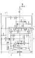
- FIG. 8 is a circuit diagram showing a power amplifier protection circuit according to the fifth embodiment.
- the protection circuit of the present embodiment includes a second protection circuit 31 and a current detection circuit 6 as shown in FIG.
- the configuration of the current detection circuit 6 is substantially the same as that of the current detection circuit 6 described in the fourth embodiment.
- the current detection circuit 6 when the amplitude of the current flowing through the output terminal OUT exceeds a predetermined level, the first current detection transistor Q14 is turned on, and further, the second current detection transistor Q15 is turned on. As a result, the positive power supply voltage + B is supplied to the collector of the second current detection transistor Q15.
- the second protection circuit 31 includes a third protection transistor Q3 having a collector connected to the first node 1 and an emitter connected to the output terminal OUT.
- the second protection circuit 31 includes a fourth diode D4 and a seventh resistor R7 connected between the collector of the second current detection transistor Q15 and the base of the third protection transistor Q3. Further, the second protection circuit 31 includes an eighth resistor R8 connected between the base of the third protection transistor Q3 and the output terminal OUT.
- the second protection circuit 31 includes a fourth protection transistor Q4 having a collector connected to the second node 2 and an emitter connected to the output terminal OUT.
- the second protection circuit 31 includes a fifth protection transistor Q5 whose base is connected to the collector of the second current detection transistor Q15. Further, the second protection circuit 31 includes a fifth diode D5 and a ninth resistor R9 connected between the collector of the fifth protection transistor Q5 and the base of the fourth protection transistor Q4.
- the second protection circuit 31 includes a tenth resistor R10 connected between the base of the fourth protection transistor Q4 and the output terminal OUT.
- the second protection circuit 31 includes a third node 3 to which a positive power supply voltage + B is supplied and a fourth node 4 to which a negative power supply voltage ⁇ B is supplied.
- the second protection circuit 31 includes a thermistor Th1 and an eleventh resistor R11 connected between the third node 3 and the fourth node 4. Further, the second protection circuit 31 includes a sixth diode D6 connected between the connection node 9 of the thermistor Th1 and the eleventh resistor R11 and the base of the second current detection transistor Q15.
- the second protection circuit 31 also includes a twelfth resistor R12 connected between the collector of the fifth protection transistor Q5 and the base of the second current detection transistor Q15.
- the second protection circuit 31 includes a thirteenth resistor R13 connected between the collector of the second current detection transistor Q15 and the base of the fifth protection transistor Q5, and the base and fourth node 4 of the fifth protection transistor Q5. And a fourteenth resistor R14 connected between the two.
- the first current detection transistor Q14 when an excessive current flows through the output terminal OUT, the first current detection transistor Q14 is turned on, and further the second current detection transistor Q15 is turned on. As a result, a base current flows to the base of the third protection transistor Q3 via the fourth diode D4 and the seventh resistor R7, and the third protection transistor Q3 is turned on. As a result, the first node 1 and the output terminal OUT are short-circuited, and the driving of the transistors Q10 and Q11 in the positive output stage in the SEPP circuit 40 is stopped. At the same time, the second current detection transistor Q15 turns on the fifth protection transistor Q5 via the thirteenth resistor R13.
- the fifth protection transistor Q5 turns on the fourth protection transistor Q4 via the fifth diode D5 and the ninth resistor R9. As a result, the second node 2 and the output terminal OUT are short-circuited, and the driving of the negative-side output stage transistors Q12 and Q13 in the SEPP circuit 40 is stopped. At the same time, the fifth protection transistor Q5 applies positive feedback to the second current detection transistor Q15 via the twelfth resistor R12. As a result, even if the first current detection transistor Q14 is turned off, the ON state of the second current detection transistor Q15 can be maintained.
- the temperature detecting thermistor Th1 has one terminal connected to the third node 3 and the other terminal connected to one terminal of the eleventh resistor R11.
- the other terminal of the eleventh resistor R11 is connected to the fourth node 4.
- the second protection circuit 31 when an excessive current flows through the output terminal OUT, the second protection circuit 31 is turned on, and the drive capability of the output stage of the SEPP circuit 40 can be continuously limited.
- the fifth protection transistor Q5 provides a latch function for the current detection circuit 6, the power amplifier can be more reliably protected.
- the second protection circuit 31 is turned on to stop driving the transistors at the output stage of the SEPP circuit 40. Therefore, it is possible to protect the power amplifier against temperature rise.
- the latch function for the second current detection transistor Q15 works by the fifth protection transistor Q5, so that the power amplifier can be protected more reliably than in the above-described embodiments.
- the thermistor generally used is a negative characteristic thermistor, and its resistance value change is not as steep as the positive characteristic thermistor as shown in FIG. For this reason, when the fourth resistor R4 is provided and positive feedback is applied to the second protection transistor Q2 as in the second embodiment, even if the resistance change with respect to temperature is moderate, if the value exceeds a certain value, the circuit operation is performed digitally. Can be made.
- FIG. 10 is a circuit corresponding to the circuit of the second embodiment shown in FIG.
- a thermistor Th2 having a negative characteristic is provided as the thermistor.
- the thermistor Th2 having a negative characteristic has one terminal connected to the first node 1 and the other terminal connected to the first resistor R1.
- the fourth resistor R4 is provided and positive feedback is applied to the second protection transistor Q2, even if the change in resistance with respect to the temperature of the thermistor Th2 having a negative characteristic is gradual, if the value exceeds a certain value, digitally
- the protective operation can be made to function.
- FIG. 11 is a circuit corresponding to the circuit of the third embodiment shown in FIG.
- a thermistor Th2 having a negative characteristic is provided as the thermistor.
- the thermistor Th2 having a negative characteristic has one terminal connected to the first node 1 and the other terminal connected to the first resistor R1.
- the fourth resistor R4 is provided and positive feedback is applied to the second protection transistor Q2, even if the change in resistance with respect to the temperature of the thermistor Th2 having a negative characteristic is gradual, if the value exceeds a certain value, digital The protective operation can be made to function.
- FIG. 12 is a circuit corresponding to the circuit of the fourth embodiment shown in FIG.
- a thermistor Th2 having a negative characteristic is provided as the thermistor.
- the thermistor Th2 having a negative characteristic has one terminal connected to the first node 1 and the other terminal connected to the first resistor R1.
- the fourth resistor R4 is provided and positive feedback is applied to the second protection transistor Q2. Therefore, even if the change in resistance with respect to the temperature of the negative thermistor Th2 is gradual, if it exceeds a certain value, it is digitally
- the protective operation can be made to function.
- FIG. 13 is a circuit corresponding to the circuit of the fourth embodiment shown in FIG.
- a thermistor Th2 having a negative characteristic is provided as the thermistor.
- the negative characteristic thermistor Th2 has one terminal connected to the fourth node 4 and the other terminal connected to a connection node 9 with the eleventh resistor R11.
- the twelfth resistor R12 is provided and positive feedback is applied to the second current detection transistor Q15, even if the resistance change with respect to the temperature of the thermistor Th2 having a negative characteristic is gradual, digital
- the protective operation can be made to function.
- the present invention can be used for a power amplifier and a speaker unit having the power amplifier.
- FIG. 14 illustrates a specific form of a power amplifier to which the present invention is applied and a speaker unit having the power amplifier.
- FIG. 14 is a block diagram showing the speaker unit 50.
- the speaker unit 50 is a bass-reflex type speaker unit, and a speaker 54 including a diaphragm 52 and a converter 53 is attached to a hole provided in the front surface of the cabinet 51.
- the converter 53 includes a voice coil and has a function of converting electric energy into mechanical energy to vibrate the diaphragm 52.
- the speaker unit 50 shown in FIG. 14 is a subwoofer that outputs sound in a low frequency band with relatively weak directivity.
- the present invention is not limited to this example, and can be applied to various speaker units that output sounds in other frequency bands.
- the speaker unit 50 includes a power amplifier 60 inside a cabinet 51.
- the power amplifier 60 is a power amplifier that includes the protection circuit and output circuit of any of the above-described embodiments and modifications.
- An output terminal OUT of the output circuit provided in the power amplifier 60 is connected to the converter 53 of the speaker 54. That is, the speaker 54 is the load shown in the circuit diagrams of the protection circuit and the output circuit of each embodiment and each modification described above.
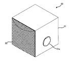
- FIG. 15 is a perspective view showing the front surface, side surface, and top surface of the speaker unit 50.
- a front grill 55 is attached to the front surface of the speaker unit 50.
- a bass reflex port 51 a is provided on the side surface of the speaker unit 50.
- FIG. 16 is a perspective view showing a state where the front grill 55 is removed from the speaker unit 50 shown in FIG.
- a speaker 54 is attached to a hole provided in the front surface of the cabinet 51.
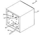
- FIG. 17 is a perspective view showing the back surface, side surface, and top surface of the speaker unit 50.
- an audio signal input terminal 56 of a power amplifier 60, a volume knob 57, a power switch 58, and a power cable 59 are provided on the back surface of the speaker unit 50.
- the audio signal input terminal 56 is connected to the input terminal IN of the output circuit provided in the power amplifier 60.
- the volume knob 57 is a knob attached to the operation unit of the volume.
- the power switch 58 is a switch for switching on and off the power source provided in the power amplifier 60.
- the power cable 59 is connected to a power source provided in the power amplifier 60 and is inserted into, for example, an AC outlet.
- SYMBOLS 10 ... Voltage amplification stage, 20 ... Bias circuit, 30 ... 1st protection circuit, 32 ... 2nd protection circuit, 40 ... SEPP circuit, 50 ... Speaker unit, 54 ... Speaker, 60 ... Power amplifier, D1 ... 1st diode D2 ... second diode, D3 ... third diode, D4 ... fourth diode, D5 ...
Landscapes
- Engineering & Computer Science (AREA)
- Power Engineering (AREA)
- Physics & Mathematics (AREA)
- Acoustics & Sound (AREA)
- Signal Processing (AREA)
- Amplifiers (AREA)
Abstract
第1ノード(1)にエミッターが接続された第1保護トランジスター(Q1)と、第1保護トランジスター(Q1)のコレクターと出力端子(OUT)との間に接続された第1ダイオード(D1)と、第2ノード(2)にエミッターが接続された第2保護トランジスター(Q2)と、第2保護トランジスター(Q2)のコレクターと出力端子(OUT)の間に接続された第2ダイオード(D2)と、第1ノード(1)と第2ノード(2)の間に接続された第1抵抗(R1)およびサーミスター(Th1)と、第1ノード(1)と第2保護トランジスター(Q2)のコレクターの間に接続された第2抵抗(R2)および第3抵抗(R3)とを備え、第1抵抗(R1)とサーミスター(Th1)により分圧された電圧が第2保護トランジスター(Q2)のベースに印加され、第2抵抗(R2)と第3抵抗(R3)により分圧された電圧が第1保護トランジスター(Q1)のベースに印加される。
Description
本発明は、パワーアンプの保護回路、パワーアンプ、およびスピーカーユニットの技術に関する。
パワーアンプの保護回路としては、例えば特許文献1のような回路が知られている。この回路は、プッシュプル出力段のエミッター抵抗の両端電圧を検出し、当該両端電圧に応じてインピーダンスが変化するトランジスターを、プッシュプル出力段のトランジスターのベースとアンプ出力との間に設けた回路である。この回路では、負荷に応じてプッシュプル出力段のドライブ能力に制限を掛け、出力端子を流れる電流の振幅を抑えることによって、プッシュプル出力段のトランジスターの発熱を抑える。
また、別の保護回路としては、例えば特許文献2のような回路が知られている。この回路では、増幅回路の出力段の電流をマイコンにより検出する。マイコンは、過電流が発生したと判別すると、保護回路を動作させる制御をする。保護回路の動作としては、例えば、ゲート回路をオフにして駆動回路への信号の入力を遮断したり、出力リレーのスイッチをオフにしてスピーカーへのオーディオ信号の出力を遮断したり、電源回路の電源出力の遮断をすること等を挙げることができる。
しかしながら、特許文献1および特許文献2の回路では、温度の検出を行っていないため、例えば放熱ファンが停止したり、放熱孔を塞がれたりした場合に温度上昇を抑えることができない。特許文献2の回路に温度検出部を設け、マイコンにより保護回路を動作させることも考えられるが、マイコンの使用により製造コストが上昇し、回路も複雑になるという問題がある。また、特許文献2のように電源回路の出力を遮断したとしても、遮断するまでの時間や、電源回路のコンデンサーに蓄積されたエネルギーの影響により、パワーアンプの回路における素子に対して大きなダメージを与えることがある。
本発明は、上述した事情に鑑みてなされたもので、その目的は、マイコンを用いることなく、過大入力、過負荷、あるいは放熱条件の悪化等の異常を確実に検出し、パワーアンプの回路における素子の破壊を防ぐこのできるパワーアンプの保護回路、パワーアンプ、およびスピーカーユニットを提供することにある。
上記目的を達成するために本発明の一態様に係るパワーアンプの保護回路は、信号が供給される第1ノードおよび第2ノードと、前記第1ノードおよび第2ノードにバイアス電圧を印加するバイアス回路と、前記第1ノードとベースが接続され出力端子から電流を出力するために用いられるダーリントン接続された複数のトランジスターと、前記第2ノードとベースが接続され前記出力端子から電流を吸い込むために用いられるダーリントン接続された複数のトランジスターとを有するプッシュプル出力回路と、を備えたパワーアンプの保護回路であって、前記第1ノードにエミッターが接続された第1保護トランジスターと、前記第1保護トランジスターのコレクターと前記出力端子との間に接続された第1ダイオードと、前記第2ノードにエミッターが接続された第2保護トランジスターと、前記第2保護トランジスターのコレクターと前記出力端子との間に接続された第2ダイオードと、前記第1ノードと前記第2ノードとの間に接続された第1抵抗およびサーミスターと、前記第1ノードと前記第2保護トランジスターのコレクターとの間に接続された第2抵抗および第3抵抗と、を備え、前記第1抵抗および前記サーミスターによって分圧された電圧が、前記第2保護トランジスターのベースに印加され、前記第2抵抗および前記第3抵抗によって分圧された電圧が、前記第1保護トランジスターのベースに印加される、ことを特徴とする。
本発明の一態様によれば、温度が上昇してサーミスターの抵抗値が変化すると、第2保護トランジスターのベースにベース電流が流れ、第2保護トランジスターが能動状態に移行する。第2保護トランジスターが能動状態に移行すると、コレクター電流が流れ始め、第1ノードと第2ノードの間の電圧が下がり始める。この状態では第2保護トランジスターに負帰還が掛かりアナログ的な動作になるが、さらに温度が上がってサーミスターの抵抗値が上がると第2保護トランジスターは完全にオンする。その結果、第2保護トランジスターのコレクター・エミッター間電圧は約0Vとなる。したがって、出力端子と第2ノードとの間の電圧は、第2ダイオードの順電圧と等しくなる。また、出力端子から電流を吸い込むために用いられるダーリントン接続されたトランジスターのベース・エミッター間の電圧は、当該ダーリントン接続されたトランジスターをオンさせるために必要な電圧よりも小さくなる。その結果、当該ダーリントン接続されたトランジスターがオフする。それと同時に、第2保護トランジスターのコレクター・エミッター間電圧が約0Vになると、第2抵抗と第3抵抗を介して、第1保護トランジスターがオンする。第1保護トランジスターがオンすると、第1保護トランジスターのコレクター・エミッター間電圧は約0Vとなる。したがって、出力端子と第1ノードとの間の電圧は、第1ダイオードの順電圧と等しくなる。また、出力端子から電流を出力するために用いられるダーリントン接続された複数のトランジスターのベース・エミッター間の電圧は、当該ダーリントン接続された複数のトランジスターをオンさせるために必要な電圧よりも小さくなる。その結果、当該ダーリントン接続された複数のトランジスターがオフする。以上のように、本発明によれば、設定温度を超えた場合にサーミスターの抵抗値が変化し、プッシュプル出力回路のダーリントン接続された複数のトランジスターの動作を停止させることができる。したがって、放熱ファンが停止したり、あるいは放熱孔が塞がれた場合等、異常の原因を問わずにプッシュプル出力回路のダーリントン接続された複数のトランジスターを幅広く保護することができる。また、本発明は、設定温度を超えた場合には、プッシュプル出力回路のダーリントン接続された複数のトランジスターを完全に停止させるので、発熱を完全に止めることができる。さらに、マイコン等による高度な信号処理は不要であるため、製造コストを低減することができ、保護回路の適用範囲を広げることができる。
前記態様において、前記第1保護トランジスターのコレクターと、前記第2保護トランジスターのベースとの間に接続された第4抵抗をさらに備えてもよい。この態様によれば、第4抵抗が設けられているので、第1保護トランジスターが能動状態に移行し始めると、第4抵抗を介して、第2保護トランジスターのベースにベース電流が流れる。そのため、サーミスターの抵抗値が第2保護トランジスターを完全にオンさせる抵抗値に達していない場合でも、第4抵抗からのベース電流が加わり、第2保護トランジスターを完全にオンさせることができる。また、第4抵抗を設けることにより、第1保護トランジスターと第2保護トランジスターがオンしている時には、第1抵抗と第4抵抗とが並列に接続された場合と同等の状態となる。したがって、第4抵抗の値を適宜に設定することにより、所望の温度まで温度が下がってサーミスターの抵抗値が変化した場合に、第2保護トランジスターおよび第1保護トランジスターをオフさせることができる。このように、この態様によれば、動作にヒステリシスを持たせることで、第2保護トランジスターのオン・オフの状態が不安定になる温度範囲が生じることを防止することができる。さらに、温度の微妙な変化で保護回路のオンとオフが頻繁に繰り返されること等の不都合が解消される。
前記態様において、前記第1抵抗および前記サーミスターの接続ノードと、前記第2保護トランジスターのベースと間に接続された第5抵抗をさらに備えてもよい。この態様によれば、第5抵抗を設けることにより、温度が低下してサーミスターの抵抗値が変化した場合でも、第2保護トランジスターをオンにしたままにすることができ、その結果、第1保護トランジスターをオンにしたままにすることができる。したがって、保護回路が一旦オンした後、常温に戻っても保護回路がオンしたままのラッチ動作を実現することができ、第5抵抗を備えていない場合に比べてより安全な動作を実現する。
前記態様において、前記出力端子を流れる電流の振幅が所定レベルを超えたことを検出すると、前記第2保護トランジスターがオンするように、前記第2保護トランジスターのベースに所定の電圧を印加する電流制御回路を備えてもよい。この態様によれば、負荷に過大電流が流れた場合は、電流制御回路により第2保護トランジスターのベースに所定の電圧が印加され、第2保護トランジスターがオンする。したがって、保護回路がオンしてプッシュプル出力回路のダーリントン接続された複数のトランジスターの駆動を停止させる。その結果、素子の破壊が生じた場合でも、継続的に正電源電圧から負電源電圧に至る短絡電流が流れなくなり、その後の被害拡大を防止することができる。さらに、この態様によれば、パワーアンプの温度が設定温度以上に上昇した場合でも、第1保護トランジスターと第2保護トランジスターとをオンさせてプッシュプル出力回路のダーリントン接続された複数のトランジスターの駆動を停止させる。したがって、温度上昇に対してもパワーアンプを保護することができる。
前記態様において、前記電流制御回路は、前記出力端子を流れる電流の振幅が所定レベルを超えるとオンとなり、正電源電圧がコレクターに供給される電流検出トランジスターを備えた電流検出回路と、前記電流検出トランジスターのコレクターと、前記第2保護トランジスターのベースとの間に接続された第3ダイオードおよび第6抵抗とを備えてもよい。この態様によれば、負荷に過大電流が流れた場合は、電流検出トランジスターがオンし、第3ダイオードおよび第6抵抗を介して第2保護トランジスターのベースに所定の電圧が印加され、第2保護トランジスターがオンする。また、第2保護トランジスターがオンすることにより、第1保護トランジスターがオンする。このように、第1保護トランジスターと第2保護トランジスターがオンすることにより、プッシュプル出力回路のダーリントン接続されたトランジスターの駆動を停止させる。その結果、素子の破壊が生じた場合でも、継続的に正電源電圧から負電源電圧に至る短絡電流が流れなくなり、その後の被害拡大を防止することができる。さらに、この態様によれば、パワーアンプの温度が設定温度以上に上昇した場合でも第1保護トランジスターと第2保護トランジスターとをオンさせてプッシュプル出力回路のダーリントン接続されたトランジスターの駆動を停止させる。したがって、温度上昇に対してもパワーアンプを保護することができる。
前記態様において、前記サーミスターは、一方の端子が前記第2ノードに接続され、他方の端子が前記第1抵抗に接続される正特性サーミスターであってもよい。この態様によれば、正特性サーミスターは、特定の温度に対して急激に抵抗値が変化する特性となっているため、第1保護トランジスターと第2保護トランジスターとを、負特性サーミスターを用いる場合に比べてよりデジタル的に動作させることができる。したがって、パワーアンプを確実に保護することができる。
前記態様において、前記サーミスターは、一方の端子が前記第1ノードに接続され、他方の端子が前記第1抵抗に接続される負特性サーミスターであってもよい。この態様によれば、負特性サーミスターの抵抗値の変化は一般的に正特性サーミスターと比べて急峻では無い。しかし、第4抵抗を設けて第2保護トランジスターに正帰還を掛ける場合には、温度に対する抵抗の変化が緩やかでも、ある値を超えればデジタル的に第1保護トランジスターと第2保護トランジスターとを動作させることができる。
上記目的を達成するために本発明の一態様に係るパワーアンプの保護回路は、信号が供給される第1ノードおよび第2ノードと、前記第1ノードおよび第2ノードにバイアス電圧を印加するバイアス回路と、前記第1ノードとベースが接続され出力端子から電流を出力するために用いられるダーリントン接続された複数のトランジスターと、前記第2ノードとベースが接続され前記出力端子から電流を吸い込むために用いられるダーリントン接続された複数のトランジスターとを有するプッシュプル出力回路とを備えたパワーアンプの保護回路であって、前記出力端子を流れる電流の振幅が所定レベルを超えるとオンとなり、正電源電圧がコレクターに供給される電流検出トランジスターを備えた電流検出回路と、前記第1ノードにコレクターが接続され、前記出力端子にエミッターが接続された第3保護トランジスターと、前記電流検出トランジスターのコレクターと前記第3保護トランジスターのベースとの間に接続された、第4ダイオードおよび第7抵抗と、前記第3保護トランジスターのベースと前記出力端子との間に接続された第8抵抗と、前記第2ノードにコレクターが接続され、前記出力端子にエミッターが接続された第4保護トランジスターと、ベースが電流検出トランジスターのコレクターと接続された第5保護トランジスターと、前記第5保護トランジスターのコレクターと第4保護トランジスターのベースとの間に接続された第5ダイオードおよび第9抵抗と、前第4保護トランジスターのベースと前記出力端子との間に接続された第10抵抗と、前記正電源電圧が供給される第3ノードと、負電源電圧が供給される第4ノードと、前記第3ノードと前記第4ノードとの間に接続されたサーミスターおよび第11抵抗と、前記サーミスターおよび第11抵抗の接続ノードと電流検出トランジスターのベースとの間に接続された第6ダイオードと、前記第5保護トランジスターのコレクターと前記電流検出トランジスターのベースとの間に接続された第12抵抗と、を備える、ことを特徴とする。
本発明の一態様によれば、出力端子に過大電流が流れると、電流検出トランジスターがオンし、第4ダイオードと第7抵抗を介して第3保護トランジスターのベースにベース電流が流れ、第3保護トランジスターがオンする。したがって、第1ノードと出力端子とは短絡し、プッシュプル出力回路においては、第1ノードとベースとが接続され出力端子から電流を出力するために用いられるトランジスターがオフする。それと同時に、電流検出トランジスターがオンすることにより、第5保護トランジスターがオンする。第5保護トランジスターがオンすることより、第5ダイオードと第9抵抗とを介して第4保護トランジスターがオンする。したがって、第2ノードと出力端子とは短絡し、プッシュプル出力回路においては、第2ノードとベースとが接続され出力端子から電流を吸い込むために用いられるトランジスターがオフする。それと同時に、第5保護トランジスターがオンすることにより、第12抵抗を介して、電流検出トランジスターに正帰還が掛かる。その結果、電流検出トランジスターの検出出力が無くなっても、電流検出トランジスターのオンを保持し続けることができる。また、パワーアンプの温度が上昇して、サーミスターの抵抗値が変化して所定値になった場合には、第6ダイオードを介して電流検出トランジスターがオンする。これ以降は上述したように、プッシュプル出力回路において、第1ノードとベースとが接続され出力端子から電流を出力するために用いられるトランジスターと、第2ノードとベースとが接続され出力端子から電流を吸い込むために用いられるトランジスターがオフする。以上のように、本発明の一態様によれば、負荷に過電流が流れた場合、およびパワーアンプの温度が設定温度以上に上昇した場合に、プッシュプル出力回路のトランジスターをオフさせる。したがって、異常が発生した要因に拘わらず、パワーアンプを保護することができ、保護を継続することができる。
本発明は、パワーアンプの保護回路のほか、当該パワーアンプの保護回路を有するパワーアンプ、および当該パワーアンプを有するスピーカーユニットとして概念することも可能である。
以下、本発明の実施形態について図面を参照して説明する。
<第1実施形態>
図1は、第1実施形態に係るパワーアンプの出力回路と当該パワーアンプの保護回路を示す回路図である。図1に示すように、パワーアンプの出力回路には、電圧増幅段10、バイアス回路20、およびSEPP回路40が備えられている。
プッシュプル出力回路としてのSEPP(Single Ended Push-Pull、シングル・エンデッド・プッシュプル)回路40は、トランジスターQ10、Q11、Q12、およびQ13と、抵抗R20、R21、およびR22を備えている。
NPN型のトランジスターQ10とNPN型のトランジスターQ11はダーリントン接続されたトランジスターである。NPN型のトランジスターQ10のベースは、信号が供給される第1ノード1に接続され、NPN型のトランジスターQ11とダーリントン接続される。トランジスターQ10とトランジスターQ11は、出力端子OUTから電流を出力するために用いられるトランジスターである。トランジスターQ10とトランジスターQ11のコレクターは、正電源電圧+Bが供給される第3ノード3に接続される。
PNP型のトランジスターQ12とPNP型のトランジスターQ13はダーリントン接続されたトランジスターである。PNP型のトランジスターQ12のベースは、信号が供給される第2ノード2に接続され、PNP型のトランジスターQ13とダーリントン接続される。トランジスターQ12とトランジスターQ13は、出力端子OUTから電流を吸い込むために用いられるトランジスターである。トランジスターQ12とトランジスターQ13のコレクターは、負電源電圧-Bが供給される第4ノード4に接続される。
<第1実施形態>
図1は、第1実施形態に係るパワーアンプの出力回路と当該パワーアンプの保護回路を示す回路図である。図1に示すように、パワーアンプの出力回路には、電圧増幅段10、バイアス回路20、およびSEPP回路40が備えられている。
プッシュプル出力回路としてのSEPP(Single Ended Push-Pull、シングル・エンデッド・プッシュプル)回路40は、トランジスターQ10、Q11、Q12、およびQ13と、抵抗R20、R21、およびR22を備えている。
NPN型のトランジスターQ10とNPN型のトランジスターQ11はダーリントン接続されたトランジスターである。NPN型のトランジスターQ10のベースは、信号が供給される第1ノード1に接続され、NPN型のトランジスターQ11とダーリントン接続される。トランジスターQ10とトランジスターQ11は、出力端子OUTから電流を出力するために用いられるトランジスターである。トランジスターQ10とトランジスターQ11のコレクターは、正電源電圧+Bが供給される第3ノード3に接続される。
PNP型のトランジスターQ12とPNP型のトランジスターQ13はダーリントン接続されたトランジスターである。PNP型のトランジスターQ12のベースは、信号が供給される第2ノード2に接続され、PNP型のトランジスターQ13とダーリントン接続される。トランジスターQ12とトランジスターQ13は、出力端子OUTから電流を吸い込むために用いられるトランジスターである。トランジスターQ12とトランジスターQ13のコレクターは、負電源電圧-Bが供給される第4ノード4に接続される。
電圧増幅段10は、第3ノード3および第4ノード4に接続され、入力端子INから入力信号を所定の電圧に増幅して得た信号を第1ノード1および第2ノード2に供給する。
バイアス回路20は、第1ノード1および第2ノード2に接続され、第1ノード1および第2ノード2に所定のバイアス電圧を印加する。これにより、SEPP回路40におけるクロスオーバー歪が減少することになる。
バイアス回路20は、第1ノード1および第2ノード2に接続され、第1ノード1および第2ノード2に所定のバイアス電圧を印加する。これにより、SEPP回路40におけるクロスオーバー歪が減少することになる。
パワーアンプの保護回路としての第1保護回路30は、PNP型の第1保護トランジスターQ1と、NPN型の第2保護トランジスターQ2とを備える。第1保護トランジスターQ1のエミッターは、第1ノード1に接続される。第2保護トランジスターQ2のエミッターは、第2ノード2に接続される。
第1保護トランジスターQ1のコレクターと、出力端子OUTとの間には、第1ダイオードD1が接続される。第2保護トランジスターQ2のコレクターと、出力端子OUTとの間には、第2ダイオードD2が接続される。信号がプラス側およびマイナス側に振れて、出力端子に接続された負荷に負荷電流が流れた時、電流に応じて抵抗R21や抵抗R22の両端に電圧降下が生じるが、その電圧降下による電圧はバイアス回路の電圧を超えることがある。例えばトランジスターQ11、抵抗R21、および負荷の経路で電流が流れた場合、抵抗R21の両端に生じる電圧降下が大きくなり、出力端子OUTは第2ノード2より低い電位になることがある。このような場合に、抵抗R2と抵抗R3に電流が流れて第1保護トランジスターQ1が誤動作することを阻止する必要がある。また、第1保護トランジスターQ1や第2保護トランジスターQ2のコレクター・ベースに間に電流が流れて、これらのトランジスターが誤動作することを阻止する必要がある。そこで、第1ダイオードD1と第2ダイオードD2を、上述したように接続している。なお、これらのダイオードにより、第1保護トランジスターQ1と第2保護トランジスターQ2がオンした場合に、第1ノード1と第2ノード2の間の電圧が、約1.2V程度に保持される。
第1保護トランジスターQ1のコレクターと、出力端子OUTとの間には、第1ダイオードD1が接続される。第2保護トランジスターQ2のコレクターと、出力端子OUTとの間には、第2ダイオードD2が接続される。信号がプラス側およびマイナス側に振れて、出力端子に接続された負荷に負荷電流が流れた時、電流に応じて抵抗R21や抵抗R22の両端に電圧降下が生じるが、その電圧降下による電圧はバイアス回路の電圧を超えることがある。例えばトランジスターQ11、抵抗R21、および負荷の経路で電流が流れた場合、抵抗R21の両端に生じる電圧降下が大きくなり、出力端子OUTは第2ノード2より低い電位になることがある。このような場合に、抵抗R2と抵抗R3に電流が流れて第1保護トランジスターQ1が誤動作することを阻止する必要がある。また、第1保護トランジスターQ1や第2保護トランジスターQ2のコレクター・ベースに間に電流が流れて、これらのトランジスターが誤動作することを阻止する必要がある。そこで、第1ダイオードD1と第2ダイオードD2を、上述したように接続している。なお、これらのダイオードにより、第1保護トランジスターQ1と第2保護トランジスターQ2がオンした場合に、第1ノード1と第2ノード2の間の電圧が、約1.2V程度に保持される。
第1ノード1と第2ノード2との間には、第1抵抗R1とサーミスターTh1とが直列接続される。第1抵抗R1とサーミスターTh1との間の接続ノード7は、第2保護トランジスターQ2のベースに接続され、第1抵抗R1とサーミスターTh1により分圧された所定の電圧が第2保護トランジスターQ2のベースに印加される。第1抵抗R1とサーミスターTh1は、サーミスターTh1により検出されるパワーアンプの温度が所定の温度に達した場合に、第2保護トランジスターQ2をオンするために用いられる。なお、サーミスターTh1は、温度が高いほど抵抗値が増加する正特性のサーミスターである。
第1ノード1と第2保護トランジスターQ2のコレクターとの間には、第2抵抗R2と第3抵抗R3が直列接続される。第2抵抗R2と第3抵抗R3の接続ノード8は、第1保護トランジスターQ1のベースに接続され、第2抵抗R2と第3抵抗R3により分圧された所定の電圧が第1保護トランジスターQ1のベースに印加される。第2抵抗R2と第3抵抗R3は、第2保護トランジスターQ2がオンした場合に、第1保護トランジスターQ1をオンするために用いられる。
次に、本実施形態における第1保護回路30の動作について説明する。以下の説明では、トランジスターが能動状態であるとは当該トランジスターが活性領域で動作することを意味する。トランジスターがオンするとは当該トランジスターが飽和領域で動作することを意味する。トランジスターがオフするとは当該トランジスターが遮断領域で動作することを意味する。なお、本実施形態では、一例として、100℃で第1保護回路30が動作するように設定されているものとする。また、サーミスターTh1の抵抗値は、100℃で10KΩであるとする。さらに、バイアス回路20の両端間の電圧、即ち、第1ノード1と第2ノード2との間の電圧は、SEPP回路40のトランジスターQ11とトランジスターQ13が能動状態になる際のベース・エミッター電圧Vbeのほぼ4個分に設定されているものとする。トランジスターQ11とトランジスターQ13が能動状態になる際のベース・エミッター電圧Vbeを約0.6Vとすれば、第1ノード1と第2ノード2との間の電圧は、約2.4Vとなる。
100℃で第2保護トランジスターQ2を能動状態に移行させるには、第1抵抗R1とサーミスターTh1との分圧による電圧が、約0.6V以上あればよい。したがって、以下の式が成立する。
100℃で第2保護トランジスターQ2を能動状態に移行させるには、第1抵抗R1とサーミスターTh1との分圧による電圧が、約0.6V以上あればよい。したがって、以下の式が成立する。
0.6[V]=2.4[V]×(サーミスターTh1の抵抗値)/(第1抵抗R1の抵抗値+サーミスターTh1の抵抗値)…式1
前記式1を変形すれば、第1抵抗R1の抵抗値を求める式は以下のようになる。
第1抵抗R1の抵抗値=(2.4[V]×(サーミスターTh1の抵抗値)/0.6[V]-(サーミスターTh1の抵抗値)…式2
100℃の際のサーミスターTh1の抵抗値を10KΩとすると、第1抵抗R1の抵抗値は以下のようになる。
第1抵抗R1の抵抗値=(2.4[V]×10[KΩ]/0.6[V]-10[KΩ]=30[KΩ]…式3
このような値に第1抵抗R1の抵抗値を設定しておくことにより、常温から100℃に変化するとサーミスターTh1の抵抗値が変化して、第2保護トランジスターQ2のベースに電流が流れ始め、第2保護トランジスターQ2が能動状態に移行する。第2保護トランジスターQ2が能動状態になり、コレクター電流が流れ始め、第1ノード1と第2ノード2との間の電圧が下がり始める。この状態では第2保護トランジスターQ2に負帰還が掛かりアナログ的な動作になるが、この状態では第2保護トランジスターQ2に負帰還が掛かりアナログ的な動作になるが、さらに温度が上がってサーミスターTh1の抵抗値が上がると第2保護トランジスターQ2は完全にオンする。その結果、第2保護トランジスターQ2のコレクター・エミッター間電圧Vceは約0Vとなる。その結果、出力端子OUTと第2ノード2との間の電圧は、第2ダイオードD2の順電圧である約0.6Vになる。同様に、第2ノード2に接続されたトランジスターQ12のベースと、抵抗R22を介して出力端子OUTに接続されたトランジスターQ13のエミッターとの間の電圧も約0.6Vになる。この約0.6Vという電圧は、トランジスターQ12が能動状態になる際のベース・エミッター電圧Vbeと、トランジスターQ13が能動状態になる際のベース・エミッター電圧Vbeとの合計である約1.2Vよりも小さい。したがって、トランジスターQ12とトランジスターQ13はオフする。
それと同時に、第2保護トランジスターQ2がオンすることにより、第2抵抗R2と第3抵抗R3を介して、第1保護トランジスターQ1がオンする。第1保護トランジスターQ1がオンすると、第1保護トランジスターQ1のコレクター・エミッター間電圧Vceは約0Vとなる。その結果、出力端子OUTと第1ノード1との間の電圧は、第1ダイオードD1の順電圧である約0.6Vになる。同様に、第1ノード2に接続されたトランジスターQ10のベースと、抵抗R21を介して出力端子OUTに接続されたトランジスターQ11のエミッターとの間の電圧も約0.6Vになる。この約0.6Vという電圧は、トランジスターQ10が能動状態になる際のベース・エミッター電圧Vbeと、トランジスターQ11が能動状態になる際のベース・エミッター電圧Vbeとの合計である約1.2Vよりも小さい。したがって、トランジスターQ10とトランジスターQ11はオフする。なお、第2抵抗R2と第3抵抗R3の抵抗値はそれぞれ、第1保護トランジスターQ1をオンすることができ、かつ、他の回路動作に悪影響を与えない範囲で自由に選ぶことができる。
以上のように、本実施形態の第1保護回路30によれば、パワーアンプの温度が設定温度を超え、サーミスターTh1の抵抗値が変化して所定値になった場合には、SEPP回路40の出力段のトランジスターの動作を停止させることができる。したがって、放熱ファンが停止したり、あるいは放熱孔が塞がれた場合等、異常の原因を問わずにSEPP回路40の出力段のトランジスターを幅広く保護することができる。また、本実施形態の第1保護回路30によれば、設定温度を超えた場合には、SEPP回路40の出力段のトランジスターを完全に停止させるので、発熱を完全に止めることができる。さらに、マイコン等による高度な信号処理は不要であるため、製造コストを低減することができ、第1保護回路30の適用範囲を広げることができる。
<第2実施形態>
次に、添付図面を参照しつつ、本発明の第2実施形態を説明する。図2は、第2実施形態に係るパワーアンプの第1保護回路30を示す回路図である。図2に示すように、本実施形態の第1保護回路30では、第1保護トランジスターQ1のコレクターと、第2保護トランジスターQ2のベースとの間には、第4抵抗R4が接続されている。
第1実施形態の第1保護回路30において、第1保護トランジスターQ1と第2保護トランジスターQ2が完全にオンになった場合には、第1保護トランジスターQ1と第2保護トランジスターQ2のコレクター・エミッターとの間の電圧はほぼ0Vになる。この時、第1ノード1と第2ノード2との間の電圧は、第1ダイオードD1と第2ダイオードD2の順電圧に依存し、約1.2V程度になる。第2保護トランジスターQ2を能動状態にするには、第1抵抗R1とサーミスターTh1との分圧による電圧が、約0.6V以上あれば良い。したがって、以下の式が成立する。
次に、添付図面を参照しつつ、本発明の第2実施形態を説明する。図2は、第2実施形態に係るパワーアンプの第1保護回路30を示す回路図である。図2に示すように、本実施形態の第1保護回路30では、第1保護トランジスターQ1のコレクターと、第2保護トランジスターQ2のベースとの間には、第4抵抗R4が接続されている。
第1実施形態の第1保護回路30において、第1保護トランジスターQ1と第2保護トランジスターQ2が完全にオンになった場合には、第1保護トランジスターQ1と第2保護トランジスターQ2のコレクター・エミッターとの間の電圧はほぼ0Vになる。この時、第1ノード1と第2ノード2との間の電圧は、第1ダイオードD1と第2ダイオードD2の順電圧に依存し、約1.2V程度になる。第2保護トランジスターQ2を能動状態にするには、第1抵抗R1とサーミスターTh1との分圧による電圧が、約0.6V以上あれば良い。したがって、以下の式が成立する。
0.6[V]=1.2[V]×(サーミスターTh1の抵抗値)/(第1抵抗R1の抵抗値+サーミスターTh1の抵抗値)…式4
前記式4を変形すれば、サーミスターTh1の抵抗値を求める式は以下のようになる。
サーミスターTh1の抵抗値=(0.6[V]×(第1抵抗R1の抵抗値))/0.6…式5
第1実施形態で説明したように、第1抵抗R1の抵抗値は30[KΩ]なので、この時のサーミスターTh1の抵抗値は以下のようになる。
サーミスターTh1の抵抗値=(0.6[V]×30[KΩ])/0.6=30[KΩ]…式6
つまり、サーミスターTh1の抵抗値が30[KΩ]程にならないと、第2保護トランジスターQ2は完全にオンにならないことになる。サーミスターTh1の抵抗値が30[KΩ]になるのは、図3に示すように100℃からもう少し高い温度、例えば、105℃辺りとなる。したがって、温度が105℃に達するまでは、第1実施形態の第1保護回路30はアナログ的な動作をしていることになる。
しかし、本実施形態では、第4抵抗R4が設けられているので、第1保護トランジスターQ1が能動状態に移行し始めると、第4抵抗R4を介して、第2保護トランジスターQ2のベースにベース電流が流れる。そのため、第2保護トランジスターQ2が能動状態になる100℃付近のサーミスターTh1の抵抗値が10[KΩ]であっても、第4抵抗R4からのベース電流が加わり、図4に示すように第2保護トランジスターQ2を完全にオンさせることができる。
第1抵抗R1と第4抵抗R4の並列の抵抗値を前記式4に当てはめると次式のようになる。
0.6[V]=1.2[V]×(サーミスターTh1の抵抗値)/(第1抵抗R1と第4抵抗R4の並列の抵抗値+サーミスターTh1の抵抗値)…式7
前記式7を変形すれば、第1抵抗R1と第4抵抗R4の並列の抵抗値は次式で求められる。
第1抵抗R1と第4抵抗R4の並列の抵抗値=1.2[V]×(サーミスターTh1の抵抗値)/0.6V[V]-(サーミスターTh1の抵抗値)…式8
サーミスターTh1の抵抗値が10[KΩ]であるとすると、第1抵抗R1と第4抵抗R4の並列の抵抗値は次のようになる。
第1抵抗R1と第4抵抗R4の並列の抵抗値=(1.2[V]×10[KΩ]/0.6V[V])-10[KΩ]=10[KΩ]…式9
第1抵抗R1は30[KΩ]なので、第4抵抗R4は15[KΩ]となる。したがって、第4抵抗R4として15[KΩ]以下の抵抗を用いることにより、第1保護トランジスターQ1が能動状態に移行し始めた時点の温度で、完全に第1保護トランジスターQ1と第2保護トランジスターQ2とをオンさせることができる。
また、第4抵抗R4が無い場合は、温度が下がっていった時、上述のオンの時と同様のアナログ的な動作が行われることにより105℃~100℃辺りで第2保護トランジスターQ2のベース電流が流れなくなる。その結果、第1保護回路30の第1保護トランジスターQ1と第2保護トランジスターQ2がオフする。しかし、第4抵抗R4があることで、第1保護トランジスターQ1がオンしている時には、第1抵抗R1と第4抵抗R4とが並列に接続された場合と同等となっている。したがって、105℃~100℃辺りの温度よりもさらに低い温度にならないと第1保護回路30の第2保護トランジスターQ2はオフしない。例えば、サーミスターTh1が1KΩ以下になった時に第1保護回路30の第2保護トランジスターQ2をオフさせたい場合には、第1抵抗R1と第4抵抗R4の並列の抵抗値は以下のようになる。前記式2のサーミスターTh1の抵抗値を1KΩとし、また前記式2における「第1抵抗R1の抵抗値」を「第1抵抗R1と第4抵抗R4の並列の抵抗値」に置き換える。
第1抵抗R1と第4抵抗R4の並列の抵抗値=(2.4[V]×1[KΩ]/0.6V[V])-1[KΩ]=3[KΩ]…式10
したがって、第1抵抗R1は30[KΩ]なので、第4抵抗R4は3.3[KΩ]となる。第4抵抗R4を3.3[KΩ]にすることにより、図4に示すように、100℃よりも低い温度に下がった時に第1保護回路30の第2保護トランジスターQ2をオフさせることができる。このように、本実施形態においては、動作にヒステリシスを持たせることで、第2保護トランジスターQ2のオン・オフの状態が不安定になる温度範囲が生じることを防止することができる。また、その範囲で第1保護トランジスターQ1と第2保護トランジスターQ2が同時にオン・オフせずに、プラス側とマイナス側で温度に対する第1保護回路30の動作が違ってくることを防止することができる。さらに、温度の微妙な変化で第1保護回路30の第1保護トランジスターQ1と第2保護トランジスターQ2とのオンとオフが頻繁に繰り返されること等の不都合が解消される。
<第3実施形態>
次に、添付図面を参照しつつ、本発明の第3実施形態を説明する。図5は、第3実施形態に係るパワーアンプの第1保護回路30を示す回路図である。図5に示すように、本実施形態においては、第1抵抗R1およびサーミスターTh1との間の接続ノード7と、第2保護トランジスターQ2のベースとの間に接続された第5抵抗R5をさらに備える。
第2実施形態では、第4抵抗R4を加えて、第1保護回路30のオンとオフの間にヒステリシス動作を付加した。本実施形態では、図5のように第5抵抗R5を加えることで、第1保護回路30が一旦オンした後、常温に戻っても第1保護回路30がオンしたままのラッチ動作にすることができる。
次に、添付図面を参照しつつ、本発明の第3実施形態を説明する。図5は、第3実施形態に係るパワーアンプの第1保護回路30を示す回路図である。図5に示すように、本実施形態においては、第1抵抗R1およびサーミスターTh1との間の接続ノード7と、第2保護トランジスターQ2のベースとの間に接続された第5抵抗R5をさらに備える。
第2実施形態では、第4抵抗R4を加えて、第1保護回路30のオンとオフの間にヒステリシス動作を付加した。本実施形態では、図5のように第5抵抗R5を加えることで、第1保護回路30が一旦オンした後、常温に戻っても第1保護回路30がオンしたままのラッチ動作にすることができる。
前記式3で計算したように、第1抵抗R1を30[KΩ]として、第1保護回路30の動作開始温度を100℃辺りと想定する。第1保護トランジスターQ1および第2保護トランジスターQ2がオンした後、温度が低下しサーミスターTh1の抵抗値がほぼ0Ωに近づいた時にも、第1保護トランジスターQ1および第2保護トランジスターQ2がオンし続けるように第4抵抗R4と第5抵抗R5の抵抗値を設定する。
第1保護トランジスターQ1のコネクター・エミッター電圧を0Vとして、サーミスターTh1を0Ωと仮定すれば、第4抵抗R4と第5抵抗R5の関係は、第2実施形態で説明した第1抵抗R1とサーミスターTh1の関係と同じである。また、第1保護トランジスターQ1と第2保護トランジスターQ2がオンした状態の想定なので、第1ノード1と第2ノード2との間の電圧は約1.2Vとなる。
第1保護トランジスターQ1のコネクター・エミッター電圧を0Vとして、サーミスターTh1を0Ωと仮定すれば、第4抵抗R4と第5抵抗R5の関係は、第2実施形態で説明した第1抵抗R1とサーミスターTh1の関係と同じである。また、第1保護トランジスターQ1と第2保護トランジスターQ2がオンした状態の想定なので、第1ノード1と第2ノード2との間の電圧は約1.2Vとなる。
0.6[V]=1.2[V]×(第5抵抗R5の抵抗値)/(第4抵抗R4の抵抗値+第5抵抗R5の抵抗値)…式11
ここで、第4抵抗R4の抵抗値を、第2実施形態で説明したように3.3KΩとする。
0.6[V]=1.2[V]×(第5抵抗R5の抵抗値)/(3.3[KΩ]+第5抵抗R5)…式12
前記式12を変形すれば、第5抵抗R5の抵抗値は次式で求められる。
(第5抵抗R5の抵抗値)=(3.3[KΩ]×0.6[V])/0.6[V]=3.3[KΩ]…式13
したがって、第5抵抗R5の抵抗値を3.3KΩ以上にしておけば、図6に示すように、例え温度が下がってサーミスターTh1が低い抵抗値になっても、第1保護回路30の第1保護トランジスターQ1と第2保護トランジスターQ2はオンし続ける。その結果、SEPP回路40の出力段のトランジスターの保護の状態は保持されることになる。なお、第1保護回路30の第1保護トランジスターQ1と第2保護トランジスターQ2をオフするには、例えば電源を一旦切断すればよい。
本実施形態によれば、第5抵抗R5を加えることで、第1保護トランジスターQ1と第2保護トランジスターQ2が一旦オンした後、常温に戻っても第1保護トランジスターQ1と第2保護トランジスターQ2とがオンしたままのラッチ動作を実現することができる。その結果、第1保護回路30によるSEPP回路40の出力段のトランジスターの保護動作は使用者が電源を切断するまで継続され、第2実施形態に比べてより安全な動作を実現する。
本実施形態によれば、第5抵抗R5を加えることで、第1保護トランジスターQ1と第2保護トランジスターQ2が一旦オンした後、常温に戻っても第1保護トランジスターQ1と第2保護トランジスターQ2とがオンしたままのラッチ動作を実現することができる。その結果、第1保護回路30によるSEPP回路40の出力段のトランジスターの保護動作は使用者が電源を切断するまで継続され、第2実施形態に比べてより安全な動作を実現する。
<第4実施形態>
次に、添付図面を参照しつつ、本発明の第4実施形態を説明する。図7は、第4実施形態に係るパワーアンプの保護回路を示す回路図である。本実施形態のパワーアンプの保護回路は、図7に示すように、第1保護回路30と電流制御回路5とを備えている。また、本実施形態においては、出力端子OUTの後段にリレーRL1が設けられており、電流制御回路5の動作によってリレーRL1がオフになるように構成されている。
上述した実施形態では、温度を検出してパワーアンプを保護する機能を実現した。したがって、例えば過大入力等で電流が増え、温度が上昇する場合には、第1保護回路30による保護動作を行うことができる。しかし、負荷が短絡する等して一瞬にして出力段のトランジスターの破壊にまで至る場合には、温度検出による保護動作だけでは対応できない。そこで、本実施形態においては、電流制御回路5を第3実施形態の回路に取り込んで、パワーアンプの保護動作を行う。
次に、添付図面を参照しつつ、本発明の第4実施形態を説明する。図7は、第4実施形態に係るパワーアンプの保護回路を示す回路図である。本実施形態のパワーアンプの保護回路は、図7に示すように、第1保護回路30と電流制御回路5とを備えている。また、本実施形態においては、出力端子OUTの後段にリレーRL1が設けられており、電流制御回路5の動作によってリレーRL1がオフになるように構成されている。
上述した実施形態では、温度を検出してパワーアンプを保護する機能を実現した。したがって、例えば過大入力等で電流が増え、温度が上昇する場合には、第1保護回路30による保護動作を行うことができる。しかし、負荷が短絡する等して一瞬にして出力段のトランジスターの破壊にまで至る場合には、温度検出による保護動作だけでは対応できない。そこで、本実施形態においては、電流制御回路5を第3実施形態の回路に取り込んで、パワーアンプの保護動作を行う。
本実施形態の電流制御回路5は、出力端子OUTを流れる電流の振幅が所定レベルを超えたことを検出すると、第2保護トランジスターQ2がオンするように、第2保護トランジスターQ2のベースに所定の電圧を印加する回路である。
本実施形態の電流制御回路5は、電流検出回路6と、第3ダイオードD3および第6抵抗R6とを備える。電流検出回路6は、抵抗R23、R24、R25、R26、R27、およびR28と、ダイオードD10、D11、およびD12と、第1電流検出トランジスターQ14と、第2電流検出トランジスターQ15とを備える。
出力端子OUTを流れる電流の振幅が所定レベルを超えると、第1電流検出トランジスターQ14がオンとなり、さらに第2電流検出トランジスターQ15がオンとなり、正電源電圧+Bが第2電流検出トランジスターQ15のコレクターに供給される。
第2電流検出トランジスターQ15のコレクターと、第2保護トランジスターQ2のベースとの間には、第3ダイオードD3と第6抵抗R6が接続される。
本実施形態の電流制御回路5は、電流検出回路6と、第3ダイオードD3および第6抵抗R6とを備える。電流検出回路6は、抵抗R23、R24、R25、R26、R27、およびR28と、ダイオードD10、D11、およびD12と、第1電流検出トランジスターQ14と、第2電流検出トランジスターQ15とを備える。
出力端子OUTを流れる電流の振幅が所定レベルを超えると、第1電流検出トランジスターQ14がオンとなり、さらに第2電流検出トランジスターQ15がオンとなり、正電源電圧+Bが第2電流検出トランジスターQ15のコレクターに供給される。
第2電流検出トランジスターQ15のコレクターと、第2保護トランジスターQ2のベースとの間には、第3ダイオードD3と第6抵抗R6が接続される。
本実施形態の回路において、出力端子OUTに過大電流が流れると、第1電流検出トランジスターQ14がオンし、さらに第2電流検出トランジスターQ15がオンする。その結果、第3ダイオードD3と第6抵抗R6を介して第2保護トランジスターQ2のベースにベース電流が流れ、第2保護トランジスターQ2がオンする。これ以降の動作は上述した実施形態と同様であり、第1保護回路30によりSEPP回路40の出力段のドライブ能力を持続的に制限することができる。
なお、負荷に過大電流が流れた場合はリレーRL1をオフすることでパワーアンプを保護することができる。しかし、例えばSEPP回路40の出力段の一方側のトランジスター(例えば、Q11)が短絡して壊れたとすると、リレーRL1をオフしてもスピーカー等の負荷の保護にはなるが、パワーアンプ自身の電源は遮断されない。したがって、SEPP回路40の出力段の他方側のトランジスター(例えば、Q13)も破壊され、火災等の危険が増大することがある。
しかしながら、本実施形態においては、SEPP回路40の出力段の一方側のトランジスターが壊れて過大電流が流れると、リレーRL1をオフするだけでなく、第1保護回路30がオンしてSEPP回路40の出力段の他方側のトランジスターの駆動を停止させる。したがって、継続的に正電源電圧+Bから負電源電圧-Bに至る短絡電流が流れなくなり、その後の被害拡大を防止することができる。なお、出力のDCオフセットのズレ等他の要因によって過大な電流が出力端子OUTを流れた場合でも、同様に第2保護トランジスターQ2をオンさせて、パワーアンプを保護することができる。
さらに、本実施形態によれば、パワーアンプの温度が設定温度以上に上昇した場合でも第1保護回路30をオンさせてSEPP回路40の出力段のトランジスターの駆動を停止させる。したがって、温度上昇に対してもパワーアンプを保護することができる。
<第5実施形態>
次に、添付図面を参照しつつ、本発明の第5実施形態を説明する。図8は、第5実施形態に係るパワーアンプの保護回路を示す回路図である。本実施形態の保護回路は、図8に示すように、第2保護回路31と電流検出回路6とを備えている。電流検出回路6の構成は、第4実施形態で説明した電流検出回路6とほぼ同様である。電流検出回路6は、出力端子OUTを流れる電流の振幅が所定レベルを超えると、第1電流検出トランジスターQ14がオンとなり、さらに、第2電流検出トランジスターQ15がオンとなる。その結果、第2電流検出トランジスターQ15のコレクターには、正電源電圧+Bが供給される。
次に、添付図面を参照しつつ、本発明の第5実施形態を説明する。図8は、第5実施形態に係るパワーアンプの保護回路を示す回路図である。本実施形態の保護回路は、図8に示すように、第2保護回路31と電流検出回路6とを備えている。電流検出回路6の構成は、第4実施形態で説明した電流検出回路6とほぼ同様である。電流検出回路6は、出力端子OUTを流れる電流の振幅が所定レベルを超えると、第1電流検出トランジスターQ14がオンとなり、さらに、第2電流検出トランジスターQ15がオンとなる。その結果、第2電流検出トランジスターQ15のコレクターには、正電源電圧+Bが供給される。
第2保護回路31は、第1ノード1にコレクターが接続され、出力端子OUTにエミッターが接続された第3保護トランジスターQ3を備えている。また、第2保護回路31は、第2電流検出トランジスターQ15のコレクターと第3保護トランジスターQ3のベースとの間に接続された第4ダイオードD4および第7抵抗R7とを備えている。さらに、第2保護回路31は、第3保護トランジスターQ3のベースと出力端子OUTとの間に接続された第8抵抗R8を備えている。
第2保護回路31は、第2ノード2にコレクターが接続され、出力端子OUTにエミッターが接続された第4保護トランジスターQ4を備えている。また、第2保護回路31は、ベースが第2電流検出トランジスターQ15のコレクターと接続された第5保護トランジスターQ5を備えている。さらに、第2保護回路31は、第5保護トランジスターQ5のコレクターと第4保護トランジスターQ4のベースとの間に接続された第5ダイオードD5および第9抵抗R9を備えている。第2保護回路31は、第4保護トランジスターQ4のベースと出力端子OUTとの間に接続された第10抵抗R10を備えている。
第2保護回路31は、正電源電圧+Bが供給される第3ノード3と、負電源電圧-Bが供給される第4ノード4とを備えている。また、第2保護回路31は、第3ノード3と第4ノード4との間に接続されたサーミスターTh1および第11抵抗R11を備える。さらに、第2保護回路31は、サーミスターTh1および第11抵抗R11の接続ノード9と第2電流検出トランジスターQ15のベースとの間に接続された第6ダイオードD6を備える。第2保護回路31は、また、第5保護トランジスターQ5のコレクターと第2電流検出トランジスターQ15のベースとの間に接続された第12抵抗R12を備える。さらに、第2保護回路31は、第2電流検出トランジスターQ15のコレクターと第5保護トランジスターQ5のベースとの間に接続された第13抵抗R13と、第5保護トランジスターQ5のベースと第4ノード4との間に接続された第14抵抗R14とを備える。
本実施形態の回路において、出力端子OUTに過大電流が流れると、第1電流検出トランジスターQ14がオンし、さらに第2電流検出トランジスターQ15がオンする。その結果、第4ダイオードD4と第7抵抗R7を介して第3保護トランジスターQ3のベースにベース電流が流れ、第3保護トランジスターQ3がオンする。その結果、第1ノード1と出力端子OUTは短絡し、SEPP回路40におけるプラス側の出力段のトランジスターQ10およびQ11の駆動を停止させる。それと同時に、第2電流検出トランジスターQ15は第13抵抗R13を介して第5保護トランジスターQ5をオンさせる。
第5保護トランジスターQ5は、第5ダイオードD5と第9抵抗R9を介して第4保護トランジスターQ4をオンさせる。その結果、第2ノード2と出力端子OUTは短絡し、SEPP回路40におけるマイナス側の出力段のトランジスターQ12,Q13の駆動を停止させる。それと同時に、第5保護トランジスターQ5は第12抵抗R12を介して、第2電流検出トランジスターQ15に正帰還を掛ける。その結果、仮に、第1電流検出トランジスターQ14がオフしても、第2電流検出トランジスターQ15のオン状態を保持し続けることができる。
なお、温度検出のサーミスターTh1は、一方の端子が第3ノード3に接続され、他方の端子が第11抵抗R11の一方の端子と接続される。また、第11抵抗R11の他方の端子は、第4ノード4に接続される。パワーアンプの温度が上昇して、サーミスターTh1の抵抗値が上昇すると、第6ダイオードD6を介して第2電流検出トランジスターQ15をオンさせる。これ以降は上述したように、SEPP回路40の出力段のトランジスターの駆動を停止させ、保護機能を保持したままにできる。
以上のように、本実施形態によれば、出力端子OUTに過大電流が流れると、第2保護回路31がオンし、SEPP回路40の出力段のドライブ能力を持続的に制限することができる。特に、第5保護トランジスターQ5により、電流検出回路6に対するラッチ機能を設けたので、より確実にパワーアンプの保護を行うことができる。
さらに、本実施形態によれば、パワーアンプの温度が設定温度以上に上昇した場合でも第2保護回路31をオンさせてSEPP回路40の出力段のトランジスターの駆動を停止させる。したがって、温度上昇に対してもパワーアンプを保護することができる。この場合も同様に、第5保護トランジスターQ5によって第2電流検出トランジスターQ15にに対するラッチ機能が働くので、上述した各実施形態に比べてより確実にパワーアンプの保護を行うことができる。
<変形例>
本発明は、上述した実施形態に限定されるものではなく、例えば次に述べるような各種の変形が可能である。また、次に述べる変形の態様は、任意に選択された一または複数を、適宜に組み合わせることもできる。
本発明は、上述した実施形態に限定されるものではなく、例えば次に述べるような各種の変形が可能である。また、次に述べる変形の態様は、任意に選択された一または複数を、適宜に組み合わせることもできる。
(変形例1)
上述した各実施形態においては、一方の端子が第2ノード2に接続され、他方の端子が第1抵抗R1に接続される正特性サーミスターを用いた。これは、図9に示すように、正特性サーミスターが、仕様で定まる特定の温度に対して急激に抵抗値が変化する特性となっているため、保護回路がよりデジタル的に動作するという利点からであった。
上述した各実施形態においては、一方の端子が第2ノード2に接続され、他方の端子が第1抵抗R1に接続される正特性サーミスターを用いた。これは、図9に示すように、正特性サーミスターが、仕様で定まる特定の温度に対して急激に抵抗値が変化する特性となっているため、保護回路がよりデジタル的に動作するという利点からであった。
一方、一般的に用いられているサーミスターは、負特性サーミスターであり、その抵抗値の変化は図9に示すように正特性サーミスターと比べて急峻では無い。このため、第2実施形態のように第4抵抗R4を設けて第2保護トランジスターQ2に正帰還を掛ける場合には、温度に対する抵抗の変化が緩やかでも、ある値を超えればデジタル的に回路動作させることができる。
図10は、図2に示す第2実施形態の回路に対応する回路である。図10に示す回路では、サーミスターとして、負特性のサーミスターTh2が設けられている。負特性のサーミスターTh2は、一方の端子が第1ノード1に接続され、他方の端子が第1抵抗R1に接続される。図10に示す回路では、第4抵抗R4を設けて第2保護トランジスターQ2に正帰還を掛けるので、負特性のサーミスターTh2の温度に対する抵抗の変化が緩やかでも、ある値を超えればデジタル的に保護動作を機能させることができる。
(変形例2)
図11は、図5に示す第3実施形態の回路に対応する回路である。図11に示す回路では、サーミスターとして、負特性のサーミスターTh2が設けられている。負特性のサーミスターTh2は、一方の端子が第1ノード1に接続され、他方の端子が第1抵抗R1に接続される。図11に示す回路では、第4抵抗R4を設けて第2保護トランジスターQ2に正帰還を掛けるので、負特性のサーミスターTh2の温度に対する抵抗の変化が緩やかでも、ある値を超えればデジタル的に保護動作を機能させることができる。
図11は、図5に示す第3実施形態の回路に対応する回路である。図11に示す回路では、サーミスターとして、負特性のサーミスターTh2が設けられている。負特性のサーミスターTh2は、一方の端子が第1ノード1に接続され、他方の端子が第1抵抗R1に接続される。図11に示す回路では、第4抵抗R4を設けて第2保護トランジスターQ2に正帰還を掛けるので、負特性のサーミスターTh2の温度に対する抵抗の変化が緩やかでも、ある値を超えればデジタル的に保護動作を機能させることができる。
(変形例3)
図12は、図7に示す第4実施形態の回路に対応する回路である。図12に示す回路では、サーミスターとして、負特性のサーミスターTh2が設けられている。負特性のサーミスターTh2は、一方の端子が第1ノード1に接続され、他方の端子が第1抵抗R1に接続される。図12に示す回路では、第4抵抗R4を設けて第2保護トランジスターQ2に正帰還を掛けるので、負特性のサーミスターTh2の温度に対する抵抗の変化が緩やかでも、ある値を超えればデジタル的に保護動作を機能させることができる。
図12は、図7に示す第4実施形態の回路に対応する回路である。図12に示す回路では、サーミスターとして、負特性のサーミスターTh2が設けられている。負特性のサーミスターTh2は、一方の端子が第1ノード1に接続され、他方の端子が第1抵抗R1に接続される。図12に示す回路では、第4抵抗R4を設けて第2保護トランジスターQ2に正帰還を掛けるので、負特性のサーミスターTh2の温度に対する抵抗の変化が緩やかでも、ある値を超えればデジタル的に保護動作を機能させることができる。
(変形例4)
図13は、図8に示す第4実施形態の回路に対応する回路である。図13に示す回路では、サーミスターとして、負特性のサーミスターTh2が設けられている。負特性のサーミスターTh2は、一方の端子が第4ノード4に接続され、他方の端子が第11抵抗R11との接続ノード9に接続される。図13に示す回路では、第12抵抗R12を設けて第2電流検出トランジスターQ15に正帰還を掛けるので、負特性のサーミスターTh2の温度に対する抵抗の変化が緩やかでも、ある値を超えればデジタル的に保護動作を機能させることができる。
図13は、図8に示す第4実施形態の回路に対応する回路である。図13に示す回路では、サーミスターとして、負特性のサーミスターTh2が設けられている。負特性のサーミスターTh2は、一方の端子が第4ノード4に接続され、他方の端子が第11抵抗R11との接続ノード9に接続される。図13に示す回路では、第12抵抗R12を設けて第2電流検出トランジスターQ15に正帰還を掛けるので、負特性のサーミスターTh2の温度に対する抵抗の変化が緩やかでも、ある値を超えればデジタル的に保護動作を機能させることができる。
(変形例5)
上述した各実施形態および各変形例においては、SEPP回路40の出力段のトランジスターとして、ダーリントン接続された複数のトランジスターを用いた構成について説明した。しかし、本発明はこの構成に限定される訳ではなく、単一のNPN型トランジスターと単一のPNP型トランジスターを接続した構成であってもよい。また、上述した各実施形態および各変形例においては、ダーリントン接続された複数のトランジスターとして、2段のダーリントン接続された複数のトランジスターを用いたが、3段のダーリントン接続された複数のトランジスターであってもよい。
上述した各実施形態および各変形例においては、SEPP回路40の出力段のトランジスターとして、ダーリントン接続された複数のトランジスターを用いた構成について説明した。しかし、本発明はこの構成に限定される訳ではなく、単一のNPN型トランジスターと単一のPNP型トランジスターを接続した構成であってもよい。また、上述した各実施形態および各変形例においては、ダーリントン接続された複数のトランジスターとして、2段のダーリントン接続された複数のトランジスターを用いたが、3段のダーリントン接続された複数のトランジスターであってもよい。
<応用例>
本発明は、パワーアンプおよび当該パワーアンプを有するスピーカーユニットに利用され得る。図14図17は、本発明の適用対象となるパワーアンプおよび当該パワーアンプを有するスピーカーユニットの具体的な形態を例示するものである。
本発明は、パワーアンプおよび当該パワーアンプを有するスピーカーユニットに利用され得る。図14図17は、本発明の適用対象となるパワーアンプおよび当該パワーアンプを有するスピーカーユニットの具体的な形態を例示するものである。
図14は、スピーカーユニット50を示すブロック図である。図14に示すように、スピーカーユニット50は、バスレフ型のスピーカーユニットであり、キャビネット51の前面に設けられた穴に、振動板52および変換器53からなるスピーカー54が取り付けられている。変換器53は、ボイスコイルを備え、電気エネルギーを機械エネルギーに変換して、振動板52を振動させる機能を有する。図14に示すスピーカーユニット50は、一例として、指向性が比較的に弱い低域の周波数帯の音を出力するサブウーファーである。但し、本発明はこの例に限定されるものではなく、その他の周波数帯の音を出力する様々なスピーカーユニットに適用可能である。
図14に示すように、スピーカーユニット50は、キャビネット51の内部にパワーアンプ60を備えている。パワーアンプ60は、上述した各実施形態および各変形例のいずれかの保護回路および出力回路を備えたパワーアンプである。パワーアンプ60に備えられた前記出力回路の出力端子OUTは、スピーカー54の変換器53と接続される。つまり、スピーカー54は、上述した各実施形態および各変形例の保護回路および出力回路の回路図に示した負荷である。
図15は、スピーカーユニット50の前面、側面、および上面を示す斜視図である。図15に示すように、スピーカーユニット50の前面にはフロントグリル55が取り付けられる。また、スピーカーユニット50の側面にはバスレフポート51aが設けられている。図16は、図15に示すスピーカーユニット50からフロントグリル55を取り外した状態を示す斜視図である。図16に示すように、キャビネット51の前面に設けられた穴にはスピーカー54が取り付けられている。
図17は、スピーカーユニット50の背面、側面、および上面を示す斜視図である。図17に示すように、スピーカーユニット50の背面には、パワーアンプ60のオーディオ信号入力端子56と、ボリュームノブ57と、電源スイッチ58と、電源ケーブル59が設けられている。オーディオ信号入力端子56は、パワーアンプ60に備えられた前記出力回路の入力端子INと接続される。ボリュームノブ57は、例えば、パワーアンプ60に備えられた前記出力回路の入力端子INと電圧増幅段10との間にボリュームを設けた場合に、当該ボリュームの操作部に取り付けるノブである。電源スイッチ58は、パワーアンプ60に備えられた電源のオンとオフを切り換えるスイッチである。電源ケーブル59は、パワーアンプ60に備えられた電源に接続され、例えばACコンセントに挿入される。
本応用例によれば、パワーアンプの温度が設定温度を超えた場合でも確実にパワーアンプ60の保護を行うことのできる安全なスピーカーユニット50を提供することができる。
1…第1ノード、2…第2ノード、3…第3ノード、4…第4ノード、5…電流制御回路、6…電流検出回路、7…接続ノード、8…接続ノード、9…接続ノード、10…電圧増幅段、20…バイアス回路、30…第1保護回路、32…第2保護回路、40…SEPP回路、50…スピーカーユニット、54…スピーカー、60…パワーアンプ、D1…第1ダイオード、D2…第2ダイオード、D3…第3ダイオード、D4…第4ダイオード、D5…第5ダイオード、D6…第6ダイオード、Q1…第1保護トランジスター、Q2…第2保護トランジスター、Q3…第3保護トランジスター、Q4…第4保護トランジスター、Q5…第5保護トランジスター、Q14…第1電流検出トランジスター、Q15…第2電流検出トランジスター、R1…第1抵抗、R2…第2抵抗、R3…第3抵抗、R4…第4抵抗、R5…第5抵抗、R6…第6抵抗、R7…第7抵抗、R8…第8抵抗、R9…第9抵抗、R10…第10抵抗、R11…第12抵抗、R13…第13抵抗、R14…第14抵抗、Th1…サーミスター、Th2…サーミスター。
Claims (11)
- 信号が供給される第1ノードおよび第2ノードと、前記第1ノードおよび第2ノードにバイアス電圧を印加するバイアス回路と、前記第1ノードとベースが接続され出力端子から電流を出力するために用いられるダーリントン接続された複数のトランジスターと、前記第2ノードとベースが接続され前記出力端子から電流を吸い込むために用いられるダーリントン接続された複数のトランジスターとを有するプッシュプル出力回路と、を備えたパワーアンプの保護回路であって、
前記第1ノードにエミッターが接続された第1保護トランジスターと、
前記第1保護トランジスターのコレクターと前記出力端子との間に接続された第1ダイオードと、
前記第2ノードにエミッターが接続された第2保護トランジスターと、
前記第2保護トランジスターのコレクターと前記出力端子との間に接続された第2ダイオードと、
前記第1ノードと前記第2ノードとの間に接続された第1抵抗およびサーミスターと、
前記第1ノードと前記第2保護トランジスターのコレクターとの間に接続された第2抵抗および第3抵抗と、を備え、
前記第1抵抗および前記サーミスターによって分圧された電圧が、前記第2保護トランジスターのベースに印加され、
前記第2抵抗および前記第3抵抗によって分圧された電圧が、前記第1保護トランジスターのベースに印加される、
ことを特徴とするパワーアンプの保護回路。 - 前記第1保護トランジスターのコレクターと、前記第2保護トランジスターのベースとの間に接続された第4抵抗をさらに備える、
ことを特徴とする請求項1に記載のパワーアンプの保護回路。 - 前記第1抵抗および前記サーミスターの接続ノードと、前記第2保護トランジスターのベースと間に接続された第5抵抗をさらに備える、
ことを特徴とする請求項2に記載のパワーアンプの保護回路。 - 前記出力端子を流れる電流の振幅が所定レベルを超えたことを検出すると、前記第2保護トランジスターがオンするように、前記第2保護トランジスターのベースに所定の電圧を印加する電流制御回路を備える、
ことを特徴とする請求項3に記載のパワーアンプの保護回路。 - 前記電流制御回路は、
前記出力端子を流れる電流の振幅が所定レベルを超えるとオンとなり、正電源電圧がコレクターに供給される電流検出トランジスターを備えた電流検出回路と、
前記電流検出トランジスターのコレクターと、前記第2保護トランジスターのベースとの間に接続された第3ダイオードおよび第6抵抗とを備える、
ことを特徴とする請求項4に記載のパワーアンプの保護回路。 - 前記サーミスターは、一方の端子が前記第2ノードに接続され、他方の端子が前記第1抵抗に接続される正特性サーミスターである、
ことを特徴とする請求項1ないし請求項5のいずれか一に記載のパワーアンプの保護回路。 - 前記サーミスターは、一方の端子が前記第1ノードに接続され、他方の端子が前記第1抵抗に接続される負特性サーミスターである、
ことを特徴とする請求項1ないし請求項5のいずれか一に記載のパワーアンプの保護回路。 - 信号が供給される第1ノードおよび第2ノードと、前記第1ノードおよび第2ノードにバイアス電圧を印加するバイアス回路と、前記第1ノードとベースが接続され出力端子から電流を出力するために用いられるダーリントン接続された複数のトランジスターと、前記第2ノードとベースが接続され前記出力端子から電流を吸い込むために用いられるダーリントン接続された複数のトランジスターとを有するプッシュプル出力回路とを備えたパワーアンプの保護回路であって、
前記出力端子を流れる電流の振幅が所定レベルを超えるとオンとなり、正電源電圧がコレクターに供給される電流検出トランジスターを備えた電流検出回路と、
前記第1ノードにコレクターが接続され、前記出力端子にエミッターが接続された第3保護トランジスターと、
前記電流検出トランジスターのコレクターと前記第3保護トランジスターのベースとの間に接続された、第4ダイオードおよび第7抵抗と、
前記第3保護トランジスターのベースと前記出力端子との間に接続された第8抵抗と、
前記第2ノードにコレクターが接続され、前記出力端子にエミッターが接続された第4保護トランジスターと、
ベースが電流検出トランジスターのコレクターと接続された第5保護トランジスターと、
前記第5保護トランジスターのコレクターと第4保護トランジスターのベースとの間に接続された第5ダイオードおよび第9抵抗と、
前第4保護トランジスターのベースと前記出力端子との間に接続された第10抵抗と、
前記正電源電圧が供給される第3ノードと、
負電源電圧が供給される第4ノードと、
前記第3ノードと前記第4ノードとの間に接続されたサーミスターおよび第11抵抗と、
前記サーミスターおよび第11抵抗の接続ノードと電流検出トランジスターのベースとの間に接続された第6ダイオードと、
前記第5保護トランジスターのコレクターと前記電流検出トランジスターのベースとの間に接続された第12抵抗と、を備える、
ことを特徴とするパワーアンプの保護回路。 - 信号が供給される第1ノードおよび第2ノードと、前記第1ノードおよび第2ノードにバイアス電圧を印加するバイアス回路と、前記第1ノードとベースが接続され出力端子から電流を出力するために用いられるダーリントン接続された複数のトランジスターと、前記第2ノードとベースが接続され前記出力端子から電流を吸い込むために用いられるダーリントン接続された複数のトランジスターとを有するプッシュプル出力回路と、
前記第1ノードにエミッターが接続された第1保護トランジスターと、
前記第1保護トランジスターのコレクターと前記出力端子との間に接続された第1ダイオードと、
前記第2ノードにエミッターが接続された第2保護トランジスターと、
前記第2保護トランジスターのコレクターと前記出力端子との間に接続された第2ダイオードと、
前記第1ノードと前記第2ノードとの間に接続された第1抵抗およびサーミスターと、
前記第1ノードと前記第2保護トランジスターのコレクターとの間に接続された第2抵抗および第3抵抗と、を備え、
前記第1抵抗および前記サーミスターによって分圧された電圧が、前記第2保護トランジスターのベースに印加され、
前記第2抵抗および前記第3抵抗によって分圧された電圧が、前記第1保護トランジスターのベースに印加される、
ことを特徴とするパワーアンプ。 - 信号が供給される第1ノードおよび第2ノードと、前記第1ノードおよび第2ノードにバイアス電圧を印加するバイアス回路と、前記第1ノードとベースが接続され出力端子から電流を出力するために用いられるダーリントン接続された複数のトランジスターと、前記第2ノードとベースが接続され前記出力端子から電流を吸い込むために用いられるダーリントン接続された複数のトランジスターとを有するプッシュプル出力回路と、
前記出力端子を流れる電流の振幅が所定レベルを超えるとオンとなり、正電源電圧がコレクターに供給される電流検出トランジスターを備えた電流検出回路と、
前記第1ノードにコレクターが接続され、前記出力端子にエミッターが接続された第3保護トランジスターと、
前記電流検出トランジスターのコレクターと前記第3保護トランジスターのベースとの間に接続された、第4ダイオードおよび第7抵抗と、
前記第3保護トランジスターのベースと前記出力端子との間に接続された第8抵抗と、
前記第2ノードにコレクターが接続され、前記出力端子にエミッターが接続された第4保護トランジスターと、
ベースが電流検出トランジスターのコレクターと接続された第5保護トランジスターと、
前記第5保護トランジスターのコレクターと第4保護トランジスターのベースとの間に接続された第5ダイオードおよび第9抵抗と、
前第4保護トランジスターのベースと前記出力端子との間に接続された第10抵抗と、
前記正電源電圧が供給される第3ノードと、
負電源電圧が供給される第4ノードと、
前記第3ノードと前記第4ノードとの間に接続されたサーミスターおよび第11抵抗と、
前記サーミスターおよび第11抵抗の接続ノードと電流検出トランジスターのベースとの間に接続された第6ダイオードと、
前記第5保護トランジスターのコレクターと前記電流検出トランジスターのベースとの間に接続された第12抵抗と、を備える、
ことを特徴とするパワーアンプ。 - 請求項9または10に記載のパワーアンプと、
前記出力端子に接続されたスピーカーと、
を備えるスピーカーユニット。
Priority Applications (3)
| Application Number | Priority Date | Filing Date | Title |
|---|---|---|---|
| JP2018520217A JP6648827B2 (ja) | 2016-05-30 | 2016-05-30 | パワーアンプの保護回路、パワーアンプ、およびスピーカーユニット |
| CN201680086339.5A CN109314494B (zh) | 2016-05-30 | 2016-05-30 | 功率放大器的保护电路、功率放大器以及扬声器单元 |
| PCT/JP2016/065919 WO2017208307A1 (ja) | 2016-05-30 | 2016-05-30 | パワーアンプの保護回路、パワーアンプ、およびスピーカーユニット |
Applications Claiming Priority (1)
| Application Number | Priority Date | Filing Date | Title |
|---|---|---|---|
| PCT/JP2016/065919 WO2017208307A1 (ja) | 2016-05-30 | 2016-05-30 | パワーアンプの保護回路、パワーアンプ、およびスピーカーユニット |
Publications (1)
| Publication Number | Publication Date |
|---|---|
| WO2017208307A1 true WO2017208307A1 (ja) | 2017-12-07 |
Family
ID=60478143
Family Applications (1)
| Application Number | Title | Priority Date | Filing Date |
|---|---|---|---|
| PCT/JP2016/065919 Ceased WO2017208307A1 (ja) | 2016-05-30 | 2016-05-30 | パワーアンプの保護回路、パワーアンプ、およびスピーカーユニット |
Country Status (3)
| Country | Link |
|---|---|
| JP (1) | JP6648827B2 (ja) |
| CN (1) | CN109314494B (ja) |
| WO (1) | WO2017208307A1 (ja) |
Cited By (2)
| Publication number | Priority date | Publication date | Assignee | Title |
|---|---|---|---|---|
| CN111490687A (zh) * | 2020-06-01 | 2020-08-04 | 郑州时享电子技术有限公司 | 一种逆变电源过流保护电路 |
| CN118473385A (zh) * | 2024-04-15 | 2024-08-09 | 南京大学 | 一种具备正负输入保护的推挽型控制输出电路 |
Families Citing this family (1)
| Publication number | Priority date | Publication date | Assignee | Title |
|---|---|---|---|---|
| CN111439124B (zh) * | 2020-03-18 | 2022-03-08 | 吉利汽车研究院(宁波)有限公司 | 一种分离式仪表扬声器及其控制方法 |
Citations (4)
| Publication number | Priority date | Publication date | Assignee | Title |
|---|---|---|---|---|
| JPS4724906Y1 (ja) * | 1969-10-02 | 1972-08-04 | ||
| JPS5389143U (ja) * | 1976-12-20 | 1978-07-21 | ||
| JPS56152412U (ja) * | 1980-04-14 | 1981-11-14 | ||
| JP2000124745A (ja) * | 1998-10-20 | 2000-04-28 | Sanyo Electric Co Ltd | 増幅回路およびこれを実装した混成集積回路装置 |
Family Cites Families (11)
| Publication number | Priority date | Publication date | Assignee | Title |
|---|---|---|---|---|
| GB2069266B (en) * | 1980-02-06 | 1984-05-31 | Chien San Wang | Current source amplifier |
| JPH0638217B2 (ja) * | 1985-11-30 | 1994-05-18 | 株式会社東芝 | 熱保護回路 |
| JP3783669B2 (ja) * | 2002-08-29 | 2006-06-07 | 株式会社村田製作所 | 過熱保護回路 |
| US6927626B2 (en) * | 2002-09-23 | 2005-08-09 | Harman International Industries, Incorporated | Thermal protection system for an output stage of an amplifier |
| CN100550560C (zh) * | 2004-07-15 | 2009-10-14 | 罗姆股份有限公司 | 过流保护电路 |
| JP2006094148A (ja) * | 2004-09-24 | 2006-04-06 | Denon Ltd | デジタルアンプ |
| JP2009055421A (ja) * | 2007-08-28 | 2009-03-12 | Sanyo Electric Co Ltd | 増幅回路 |
| CN101588056B (zh) * | 2009-03-11 | 2011-06-29 | 中国电子科技集团公司第二十四研究所 | 一种过热保护电路 |
| WO2014017444A1 (ja) * | 2012-07-23 | 2014-01-30 | ヤマハ株式会社 | 音響信号変換器のための温度測定装置及び保護装置 |
| CN103117718B (zh) * | 2013-01-31 | 2015-08-26 | 桂林电子科技大学 | 高保真晶体管音频功率放大器 |
| CN105391410A (zh) * | 2015-11-05 | 2016-03-09 | 晋鲁杰 | 一种功率放大器的保护电路 |
-
2016
- 2016-05-30 JP JP2018520217A patent/JP6648827B2/ja active Active
- 2016-05-30 WO PCT/JP2016/065919 patent/WO2017208307A1/ja not_active Ceased
- 2016-05-30 CN CN201680086339.5A patent/CN109314494B/zh active Active
Patent Citations (4)
| Publication number | Priority date | Publication date | Assignee | Title |
|---|---|---|---|---|
| JPS4724906Y1 (ja) * | 1969-10-02 | 1972-08-04 | ||
| JPS5389143U (ja) * | 1976-12-20 | 1978-07-21 | ||
| JPS56152412U (ja) * | 1980-04-14 | 1981-11-14 | ||
| JP2000124745A (ja) * | 1998-10-20 | 2000-04-28 | Sanyo Electric Co Ltd | 増幅回路およびこれを実装した混成集積回路装置 |
Cited By (2)
| Publication number | Priority date | Publication date | Assignee | Title |
|---|---|---|---|---|
| CN111490687A (zh) * | 2020-06-01 | 2020-08-04 | 郑州时享电子技术有限公司 | 一种逆变电源过流保护电路 |
| CN118473385A (zh) * | 2024-04-15 | 2024-08-09 | 南京大学 | 一种具备正负输入保护的推挽型控制输出电路 |
Also Published As
| Publication number | Publication date |
|---|---|
| CN109314494A (zh) | 2019-02-05 |
| CN109314494B (zh) | 2022-02-25 |
| JP6648827B2 (ja) | 2020-02-14 |
| JPWO2017208307A1 (ja) | 2019-02-28 |
Similar Documents
| Publication | Publication Date | Title |
|---|---|---|
| KR101606441B1 (ko) | 전력 증폭기의 전원 온/오프시 출력단과 스피커 보호회로 | |
| JP2006180049A (ja) | ディジタルアンプ | |
| CN109428556B (zh) | 功率放大器和用于射频主动电路的保护电路 | |
| US7719363B2 (en) | Method and apparatus for output amplifier protection | |
| JP6648827B2 (ja) | パワーアンプの保護回路、パワーアンプ、およびスピーカーユニット | |
| JPS582607B2 (ja) | 温度検知回路 | |
| CN102333264A (zh) | 静音控制电路及具有该静音控制电路的电子装置 | |
| JP4191077B2 (ja) | スピーカ保護回路およびスピーカ保護方法 | |
| JP4960734B2 (ja) | オーディオ装置の過熱保護回路 | |
| JP2008035596A (ja) | 保護回路 | |
| US3277386A (en) | Overload protection circuit for transistor amplifiers | |
| JP5638428B2 (ja) | アンテナ接続状態検出回路 | |
| US3600695A (en) | Power amplifier with overload protection | |
| JP2010288138A (ja) | 電力増幅器保護回路 | |
| CN204408284U (zh) | 一种音频功率放大器电路 | |
| JP4284102B2 (ja) | 音響用プッシュプル電力増幅回路 | |
| JP4078514B2 (ja) | 増幅回路 | |
| JP2002124837A (ja) | 増幅回路およびそれを用いた電子装置 | |
| JP6108617B2 (ja) | 電圧レギュレータ回路 | |
| JP4011435B2 (ja) | 過電流検出回路 | |
| WO2014109090A1 (ja) | 高周波増幅回路 | |
| CN223599834U (zh) | 模拟信号保护电路、音频播放设备和音视频播放设备 | |
| CN213280065U (zh) | 带有保护电路的喇叭 | |
| JPH0145152Y2 (ja) | ||
| CN210829821U (zh) | 一种控制高性能大功率功放散热风扇的电路 |
Legal Events
| Date | Code | Title | Description |
|---|---|---|---|
| ENP | Entry into the national phase |
Ref document number: 2018520217 Country of ref document: JP Kind code of ref document: A |
|
| NENP | Non-entry into the national phase |
Ref country code: DE |
|
| 121 | Ep: the epo has been informed by wipo that ep was designated in this application |
Ref document number: 16903935 Country of ref document: EP Kind code of ref document: A1 |
|
| 122 | Ep: pct application non-entry in european phase |
Ref document number: 16903935 Country of ref document: EP Kind code of ref document: A1 |