WO2017199617A1 - モジュール部品 - Google Patents
モジュール部品 Download PDFInfo
- Publication number
- WO2017199617A1 WO2017199617A1 PCT/JP2017/014160 JP2017014160W WO2017199617A1 WO 2017199617 A1 WO2017199617 A1 WO 2017199617A1 JP 2017014160 W JP2017014160 W JP 2017014160W WO 2017199617 A1 WO2017199617 A1 WO 2017199617A1
- Authority
- WO
- WIPO (PCT)
- Prior art keywords
- main electrode
- electrode
- mounting component
- main
- wiring
- Prior art date
- Legal status (The legal status is an assumption and is not a legal conclusion. Google has not performed a legal analysis and makes no representation as to the accuracy of the status listed.)
- Ceased
Links
Images














Classifications
-
- H—ELECTRICITY
- H05—ELECTRIC TECHNIQUES NOT OTHERWISE PROVIDED FOR
- H05K—PRINTED CIRCUITS; CASINGS OR CONSTRUCTIONAL DETAILS OF ELECTRIC APPARATUS; MANUFACTURE OF ASSEMBLAGES OF ELECTRICAL COMPONENTS
- H05K1/00—Printed circuits
- H05K1/02—Details
- H05K1/0286—Programmable, customizable or modifiable circuits
- H05K1/029—Programmable, customizable or modifiable circuits having a programmable lay-out, i.e. adapted for choosing between a few possibilities
-
- H—ELECTRICITY
- H05—ELECTRIC TECHNIQUES NOT OTHERWISE PROVIDED FOR
- H05K—PRINTED CIRCUITS; CASINGS OR CONSTRUCTIONAL DETAILS OF ELECTRIC APPARATUS; MANUFACTURE OF ASSEMBLAGES OF ELECTRICAL COMPONENTS
- H05K1/00—Printed circuits
- H05K1/02—Details
- H05K1/11—Printed elements for providing electric connections to or between printed circuits
- H05K1/111—Pads for surface mounting, e.g. lay-out
- H05K1/112—Pads for surface mounting, e.g. lay-out directly combined with via connections
- H05K1/113—Via provided in pad; Pad over filled via
-
- H—ELECTRICITY
- H05—ELECTRIC TECHNIQUES NOT OTHERWISE PROVIDED FOR
- H05K—PRINTED CIRCUITS; CASINGS OR CONSTRUCTIONAL DETAILS OF ELECTRIC APPARATUS; MANUFACTURE OF ASSEMBLAGES OF ELECTRICAL COMPONENTS
- H05K1/00—Printed circuits
- H05K1/02—Details
- H05K1/0213—Electrical arrangements not otherwise provided for
- H05K1/0216—Reduction of cross-talk, noise or electromagnetic interference
- H05K1/023—Reduction of cross-talk, noise or electromagnetic interference using auxiliary mounted passive components or auxiliary substances
- H05K1/0231—Capacitors or dielectric substances
-
- H—ELECTRICITY
- H05—ELECTRIC TECHNIQUES NOT OTHERWISE PROVIDED FOR
- H05K—PRINTED CIRCUITS; CASINGS OR CONSTRUCTIONAL DETAILS OF ELECTRIC APPARATUS; MANUFACTURE OF ASSEMBLAGES OF ELECTRICAL COMPONENTS
- H05K1/00—Printed circuits
- H05K1/02—Details
- H05K1/11—Printed elements for providing electric connections to or between printed circuits
- H05K1/111—Pads for surface mounting, e.g. lay-out
-
- H—ELECTRICITY
- H05—ELECTRIC TECHNIQUES NOT OTHERWISE PROVIDED FOR
- H05K—PRINTED CIRCUITS; CASINGS OR CONSTRUCTIONAL DETAILS OF ELECTRIC APPARATUS; MANUFACTURE OF ASSEMBLAGES OF ELECTRICAL COMPONENTS
- H05K1/00—Printed circuits
- H05K1/02—Details
- H05K1/11—Printed elements for providing electric connections to or between printed circuits
- H05K1/115—Via connections; Lands around holes or via connections
-
- H—ELECTRICITY
- H05—ELECTRIC TECHNIQUES NOT OTHERWISE PROVIDED FOR
- H05K—PRINTED CIRCUITS; CASINGS OR CONSTRUCTIONAL DETAILS OF ELECTRIC APPARATUS; MANUFACTURE OF ASSEMBLAGES OF ELECTRICAL COMPONENTS
- H05K1/00—Printed circuits
- H05K1/18—Printed circuits structurally associated with non-printed electric components
-
- H—ELECTRICITY
- H05—ELECTRIC TECHNIQUES NOT OTHERWISE PROVIDED FOR
- H05K—PRINTED CIRCUITS; CASINGS OR CONSTRUCTIONAL DETAILS OF ELECTRIC APPARATUS; MANUFACTURE OF ASSEMBLAGES OF ELECTRICAL COMPONENTS
- H05K2201/00—Indexing scheme relating to printed circuits covered by H05K1/00
- H05K2201/03—Conductive materials
- H05K2201/0302—Properties and characteristics in general
- H05K2201/0305—Solder used for other purposes than connections between PCB or components, e.g. for filling vias or for programmable patterns
-
- H—ELECTRICITY
- H05—ELECTRIC TECHNIQUES NOT OTHERWISE PROVIDED FOR
- H05K—PRINTED CIRCUITS; CASINGS OR CONSTRUCTIONAL DETAILS OF ELECTRIC APPARATUS; MANUFACTURE OF ASSEMBLAGES OF ELECTRICAL COMPONENTS
- H05K2201/00—Indexing scheme relating to printed circuits covered by H05K1/00
- H05K2201/10—Details of components or other objects attached to or integrated in a printed circuit board
- H05K2201/10613—Details of electrical connections of non-printed components, e.g. special leads
- H05K2201/10621—Components characterised by their electrical contacts
- H05K2201/10636—Leadless chip, e.g. chip capacitor or resistor
-
- H—ELECTRICITY
- H05—ELECTRIC TECHNIQUES NOT OTHERWISE PROVIDED FOR
- H05K—PRINTED CIRCUITS; CASINGS OR CONSTRUCTIONAL DETAILS OF ELECTRIC APPARATUS; MANUFACTURE OF ASSEMBLAGES OF ELECTRICAL COMPONENTS
- H05K2203/00—Indexing scheme relating to apparatus or processes for manufacturing printed circuits covered by H05K3/00
- H05K2203/17—Post-manufacturing processes
- H05K2203/173—Adding connections between adjacent pads or conductors, e.g. for modifying or repairing
-
- H—ELECTRICITY
- H05—ELECTRIC TECHNIQUES NOT OTHERWISE PROVIDED FOR
- H05K—PRINTED CIRCUITS; CASINGS OR CONSTRUCTIONAL DETAILS OF ELECTRIC APPARATUS; MANUFACTURE OF ASSEMBLAGES OF ELECTRICAL COMPONENTS
- H05K3/00—Apparatus or processes for manufacturing printed circuits
- H05K3/30—Assembling printed circuits with electric components, e.g. with resistors
- H05K3/32—Assembling printed circuits with electric components, e.g. with resistors electrically connecting electric components or wires to printed circuits
- H05K3/34—Assembling printed circuits with electric components, e.g. with resistors electrically connecting electric components or wires to printed circuits by soldering
- H05K3/341—Surface mounted components
- H05K3/3431—Leadless components
- H05K3/3442—Leadless components having edge contacts, e.g. leadless chip capacitors, chip carriers
-
- Y—GENERAL TAGGING OF NEW TECHNOLOGICAL DEVELOPMENTS; GENERAL TAGGING OF CROSS-SECTIONAL TECHNOLOGIES SPANNING OVER SEVERAL SECTIONS OF THE IPC; TECHNICAL SUBJECTS COVERED BY FORMER USPC CROSS-REFERENCE ART COLLECTIONS [XRACs] AND DIGESTS
- Y02—TECHNOLOGIES OR APPLICATIONS FOR MITIGATION OR ADAPTATION AGAINST CLIMATE CHANGE
- Y02P—CLIMATE CHANGE MITIGATION TECHNOLOGIES IN THE PRODUCTION OR PROCESSING OF GOODS
- Y02P70/00—Climate change mitigation technologies in the production process for final industrial or consumer products
- Y02P70/50—Manufacturing or production processes characterised by the final manufactured product
Definitions
- the present invention relates to a module component.
- circuit configurations such as electronic components and wiring are designed in advance.
- wiring is formed in the circuit board, and the circuit board is formed on the surface of the circuit board.
- Forms an electrode is formed in the circuit board.
- the mounting component is joined to the electrode by soldering to be mounted on the circuit board to form a module component.
- an object of the present invention is to provide a module component that can cope with a plurality of circuit configurations.
- one aspect of a module component according to the present invention includes a substrate, a first main electrode disposed on the main surface of the substrate, and the main surface facing the first main electrode.
- a second main electrode disposed on the main surface, a third main electrode disposed on the main surface at a position other than the position where the first main electrode and the second main electrode are provided, and the third main electrode
- the fourth main electrode disposed on the main surface so as to face each other, and any two of the first main electrode, the second main electrode, the third main electrode, and the fourth main electrode
- a first mounting component mounted on two main electrodes, and a second mounting component mounted on the third main electrode and the fourth main electrode, and the area of the sub-electrode is the first main electrode , Smaller than the area of the second main electrode, the third main electrode, and the fourth main electrode.
- any one of the first main electrode, the second main electrode, the third main electrode, and the fourth main electrode and the sub electrode are connected only by the conductive bonding member. Therefore, it is not necessary to previously form a wiring pattern for connecting any one of the first main electrode, the second main electrode, the third main electrode, and the fourth main electrode and the sub electrode on the substrate, and the arrangement of the conductive bonding member By changing the circuit configuration, the circuit configuration can be easily changed.
- the sub-electrode is provided between at least one of the first main electrode and the second main electrode and between the third main electrode and the fourth main electrode.
- the sub-electrode is disposed below the first mounting component, the second mounting component, or both on the main surface of the substrate.
- the sub-electrode is between the first main electrode and any one of the third main electrode and the fourth main electrode adjacent to the first main electrode, and the second main electrode, The third main electrode and the fourth main electrode are provided at least between one of the third main electrode and the fourth main electrode adjacent to the second main electrode.
- the sub electrode is connected to the main electrode by the conductive bonding member, it is not necessary to previously form a wiring pattern on the substrate, and the sub electrode and the main electrode are connected by the arrangement of the conductive bonding member. Can do.
- first main electrode, one of the third main electrode and the fourth main electrode adjacent to the first main electrode, the second main electrode, the third main electrode, and the At least one of the fourth main electrodes adjacent to the second main electrode is connected via the sub electrode.
- the sub electrode disposed between the two main electrodes and the main electrode are connected by the conductive bonding member, even when the distance between the two main electrodes is long, the sub electrode is interposed. Can connect two main electrodes.
- the sub-electrode is configured such that the first mounting component or the second mounting is provided via at least one of the first main electrode, the second main electrode, the third main electrode, and the fourth main electrode. Connected with parts.
- a signal such as current or voltage can be supplied from the sub electrode to the mounting component via the main electrode.
- the sub electrode is grounded.
- the sub electrode can be used as a ground electrode.
- any one of the first main electrode, the second main electrode, the third main electrode, and the fourth main electrode is connected to an input wiring.
- the wiring connected to one of the main electrodes to which the mounting component is connected can be used as the wiring for supplying the input signal to the mounting component.
- any one of the first main electrode, the second main electrode, the third main electrode, and the fourth main electrode is connected to an output wiring.
- the wiring connected to one of the main electrodes to which the mounting component is connected can be used as a wiring for outputting a signal from the mounting component.
- the sub electrode is connected to any one of the first main electrode, the second main electrode, the third main electrode, and the fourth main electrode connected to the input wiring.
- a wiring path branched from the first main electrode, the second main electrode, the third main electrode, and the fourth main electrode connected to the input wiring can be configured.
- the sub electrode is connected to any one of the first main electrode, the second main electrode, the third main electrode, and the fourth main electrode connected to the output wiring.
- a wiring path branched from the first main electrode, the second main electrode, the third main electrode, and the fourth main electrode connected to the output wiring can be configured.
- a plurality of the sub-electrodes are provided between at least one of the first main electrode and the second main electrode and between the third main electrode and the fourth main electrode.
- the bonding property between the sub electrode and the main electrode can be improved.
- the sub-electrode overlaps with the first mounting component or the second mounting component when the module component is viewed in plan and is along a side surface of the first mounting component or the second mounting component. Placed in position.
- the sub electrode is disposed at a position along the side surface of the first mounting component or the second mounting component, the sub electrode is positioned at a position that hinders the lines of magnetic force directed directly below the first mounting component or the second mounting component. Arranging the electrodes can be avoided. Thereby, the characteristic of a module component can be improved.
- One of the electrode and the fourth main electrode is connected to an output wiring, the first mounting component and the second mounting component are connected in parallel to each other, and between the input wiring and the output wiring Are connected in series.
- One of the electrode and the fourth main electrode is connected to an output wiring, the first mounting component and the second mounting component are connected in series to each other, and between the input wiring and the output wiring Are connected so as to branch from a wiring connecting the input wiring and the output wiring.
- One of the electrode and the fourth main electrode is connected to an output wiring, the first mounting component and the second mounting component are connected in parallel to each other, and between the input wiring and the output wiring Are connected so as to branch from a wiring connecting the input wiring and the output wiring.
- One of the electrode and the fourth main electrode is connected to an output wiring, the first mounting component and the second mounting component are connected in series to each other, and between the input wiring and the output wiring Are connected in series.
- a fifth main electrode disposed at a position other than a position at which the first main electrode, the second main electrode, the third main electrode, and the fourth main electrode are disposed, and opposite to the fifth main electrode.
- a third mounting component mounted on the fifth main electrode and the sixth main electrode, the first mounting component, the second mounting component, and the One of the third mounting components is connected in series between the input wiring and the output wiring, and the other one of the first mounting component, the second mounting component, and the third mounting component.
- the input wiring and the output wiring are connected between the input wiring and one of the first mounting component, the second mounting component, and the third mounting component connected in series to the input wiring.
- Branch from the wiring connecting The remaining one of the first mounting component, the second mounting component, and the third mounting component is connected to the output wiring in series with the first mounting component, the second mounting component, and One of the third mounting components and the output wiring are connected so as to branch from a wiring connecting the input wiring and the output wiring.
- the configuration of the ⁇ connection circuit can be realized by changing the connection of the first mounting component, the second mounting component, and the third mounting component on one board.
- a fifth main electrode disposed at a position other than a position at which the first main electrode, the second main electrode, the third main electrode, and the fourth main electrode are disposed, and opposite to the fifth main electrode.
- a third mounting component mounted on the fifth main electrode and the sixth main electrode, the first mounting component, the second mounting component, and the Two of the third mounting components are connected in series between the input wiring and the output wiring, and the remaining one of the first mounting component, the second mounting component, and the third mounting component.
- One of the first mounting component and the second mounting component is connected so as to branch from a wiring connecting the input wiring and the output wiring.
- the configuration of the Y connection circuit can be realized by changing the connection of the first mounting component, the second mounting component, and the third mounting component on one board.
- the second main electrode or the fourth main electrode closest to the first main electrode or the third main electrode is connected to the first main electrode or the third main electrode closest to the first main electrode or the third main electrode. It is connected without going through.
- the main electrodes since the side surfaces of the main electrodes are connected only by the conductive bonding member, it is not necessary to previously form a wiring pattern for connecting the main electrodes on the substrate, and the arrangement of the conductive bonding members is changed. By doing so, the main electrodes can be easily joined together.
- the areas of the first sub electrode and the second sub electrode are smaller than the areas of the first main electrode and the second main electrode, and the first sub electrode may be the first main electrode or the second main electrode.
- the electrode is connected by a conductive bonding member, and the second sub electrode is connected by the conductive bonding member to the first main electrode or the second main electrode to which the first sub electrode is not connected. .
- the sub electrode and the first main electrode or the second main electrode are connected only by the conductive bonding member, the sub electrode and the first main electrode or the second main electrode are connected by one substrate. There is no need to previously form a wiring pattern on the substrate, and the direction of the current flowing through the first mounting component can be easily changed by changing the arrangement of the conductive bonding members. Therefore, the magnetic field given to the surroundings by the first mounting component can be changed.
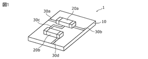
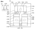
- FIG. 1 is a conceptual diagram illustrating a configuration of a module component according to the first embodiment.
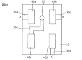
- FIG. 2A is a plan view illustrating an example of an electrode pattern of the module component according to the first embodiment.
- FIG. 2B is a plan view illustrating a connection example of the first main electrode and the first sub electrode in the module component according to the first embodiment.
- FIG. 2C is a plan view illustrating an example of a configuration in which the first mounting component and the second mounting component are mounted in the module component according to the first exemplary embodiment.
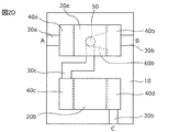
- FIG. 2D is a plan view illustrating an example of a configuration in which the first mounting component and the second mounting component are mounted in the module component according to the first embodiment.
- FIG. 1 is a conceptual diagram illustrating a configuration of a module component according to the first embodiment.
- FIG. 2A is a plan view illustrating an example of an electrode pattern of the module component according to the first embodiment.
- FIG. 2B is a plan view illustrating a connection example of the first main electrode and
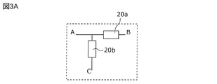
- FIG. 3A is a plan view illustrating a connection example of the first mounting component and the second mounting component in the module component according to the first embodiment.
- FIG. 3B is a plan view illustrating another connection example of the first mounting component and the second mounting component in the module component according to the first embodiment.
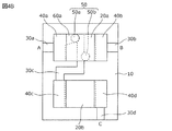
- FIG. 4A is a plan view illustrating an example of an electrode pattern of a module component according to the second embodiment.
- FIG. 4B is a plan view illustrating an example of a configuration in which the first mounting component and the second mounting component are mounted in the module component according to the second exemplary embodiment.
- FIG. 4C is a plan view illustrating an example of a configuration in which the first mounting component and the second mounting component are mounted in the module component according to the second exemplary embodiment.
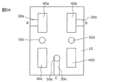
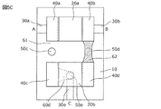
- FIG. 5A is a plan view illustrating an example of an electrode pattern of a module component according to the third embodiment.
- FIG. 5B is a plan view illustrating an example of a configuration in which the first mounting component and the second mounting component are mounted in the module component according to the third embodiment.
- FIG. 5C is a plan view illustrating an example of a configuration in which the first mounting component and the second mounting component are mounted in the module component according to the third exemplary embodiment.
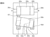
- FIG. 6A is a plan view illustrating an example of an electrode pattern of a module component according to the fourth embodiment.
- FIG. 6B is a plan view illustrating an example of a configuration in which the first mounting component and the second mounting component are mounted in the module component according to the fourth embodiment.
- FIG. 6C is a plan view illustrating an example of a configuration in which the first mounting component and the second mounting component are mounted in the module component according to the fourth embodiment.
- FIG. 7A is a plan view illustrating an example of an electrode pattern of a module component according to the fifth embodiment.
- FIG. 7B is a plan view illustrating an example of a configuration in which the first mounting component and the second mounting component are mounted in the module component according to the fifth embodiment.
- FIG. 7C is a plan view illustrating an example of a configuration in which the first mounting component and the second mounting component are mounted in the module component according to the fifth embodiment.
- FIG. 7D is a plan view illustrating an example of a configuration in which the first mounting component and the second mounting component are mounted in the module component according to the fifth embodiment.
- FIG. 7A is a plan view illustrating an example of an electrode pattern of a module component according to the fifth embodiment.
- FIG. 7B is a plan view illustrating an example of a configuration in which the first mounting component and the second
- FIG. 7E is a plan view illustrating an example of a configuration in which the first mounting component and the second mounting component are mounted in the module component according to the fifth embodiment.
- FIG. 8A is a plan view illustrating an example of an electrode pattern of a module component according to the sixth embodiment.
- FIG. 8B is a plan view illustrating an example of a configuration in which the first mounting component, the second mounting component, and the third mounting component are mounted in the module component according to the sixth embodiment.
- FIG. 8C is a plan view illustrating an example of a configuration in which the first mounting component, the second mounting component, and the third mounting component are mounted in the module component according to the sixth embodiment.
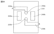
- FIG. 9A is a plan view illustrating an example of an electrode pattern of a module component according to the seventh embodiment.
- FIG. 9A is a plan view illustrating an example of an electrode pattern of a module component according to the seventh embodiment.
- FIG. 9B is a plan view illustrating an example of a configuration in which the first mounting component is mounted in the module component according to the seventh embodiment.
- FIG. 9C is a plan view illustrating an example of a configuration in which the first mounting component is mounted in the module component according to the seventh embodiment.
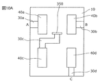
- FIG. 10A is a plan view illustrating an example of an electrode pattern of a module component according to the eighth embodiment.
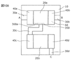
- FIG. 10B is a plan view illustrating an example of a configuration in which the first mounting component and the second mounting component are mounted in the module component according to the eighth embodiment.
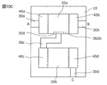
- FIG. 10C is a plan view illustrating an example of a configuration in which the first mounting component and the second mounting component are mounted in the module component according to the eighth embodiment.
- FIG. 10A is a plan view illustrating an example of an electrode pattern of a module component according to the eighth embodiment.
- FIG. 10B is a plan view illustrating an example of a configuration in which the first mounting component and the second mounting component are mounted in the module component according to
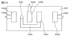
- FIG. 11A is a plan view illustrating an example of an electrode pattern of a module component according to the first modification.
- FIG. 11B is a plan view illustrating an example of a configuration in which the first mounting component and the second mounting component are mounted in the module component according to the first modification.
- 12A is a plan view illustrating an example of an electrode pattern of a module component according to Modification 2.
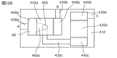
- FIG. 12B is a plan view illustrating an example of a configuration in which the first mounting component and the second mounting component are mounted in the module component according to the second modification.
- FIG. 1 is a schematic diagram showing a configuration of a module component 1 according to the present embodiment.
- the module component 1 includes a first mounting component 20a and a second mounting component 20b, wirings 30a, 30b, 30c and 30d on the main surface of the substrate 10 as shown in FIG.
- a main electrode 40a, a second main electrode 40b, a third main electrode 40c, a fourth main electrode 40d (see FIG. 2A), and a sub electrode 50 (see FIG. 2A) are provided.
- the board 10 is, for example, a printed board or a LTCC (Low Temperature Co-fired Ceramics) board.
- LTCC Low Temperature Co-fired Ceramics
- the first mounting component 20a and the second mounting component 20b are components such as a capacitor and an inductor, for example.
- the first mounting component 20a and the second mounting component 20b are provided with electrode portions at both ends so that they can be connected to the first main electrode 40a, the second main electrode 40b, the third main electrode 40c, and the fourth main electrode 40d. Yes.
- FIG. 2A is a plan view showing an example of an electrode pattern on the substrate 10 of the module component 1 according to the present embodiment.
- a first main electrode 40a, a second main electrode 40b, a third main electrode 40c, and a fourth main electrode 40d are formed on the substrate 10.
- the second main electrode is disposed so as to face the first main electrode.
- the third main electrode is disposed at a position other than the position where the first main electrode and the second main electrode are provided.
- the fourth main electrode is disposed so as to face the third main electrode, and is disposed at a position other than the position where the first main electrode, the second main electrode, and the third main electrode are provided.
- the first main electrode 40a, the second main electrode 40b, the third main electrode 40c, and the fourth main electrode 40d are made of, for example, a Cu—Ni-based material. Note that the first main electrode 40a, the second main electrode 40b, the third main electrode 40c, and the fourth main electrode 40d may be formed of other materials, for example, aluminum.
- the first main electrode 40a, the second main electrode 40b, the third main electrode 40c, and the fourth main electrode 40d have, for example, a substantially rectangular shape having a long side of 200 ⁇ m and a short side of 90 ⁇ m.
- the first main electrode 40a and the second main electrode 40b are arranged to face each other on the substrate 10 so that the long sides are substantially parallel to each other.
- the distance between the first main electrode 40a and the second main electrode 40b is, for example, 220 ⁇ m.
- the 3rd main electrode 40c and the 4th main electrode 40d are arrange
- the distance between the third main electrode 40c and the fourth main electrode 40d is, for example, 220 ⁇ m.
- the third main electrode 40c is disposed on the main surface of the substrate 10 so as to face the first main electrode 40a so that the short side thereof is substantially parallel.
- the distance between the first main electrode 40a and the third main electrode 40c is, for example, 125 ⁇ m.
- the fourth main electrode 40d is disposed on the main surface of the substrate 10 so as to face the second main electrode 40b so that the short sides thereof are substantially parallel to each other.
- the distance between the second main electrode 40b and the fourth main electrode 40d is, for example, 125 ⁇ m.
- the first main electrode 40a is connected to one end of the wiring 30a.
- the wiring 30a is made of, for example, a Cu—Ni-based material.
- the width of the wiring 30a is, for example, 75 ⁇ m.
- the other end of the wiring 30a is connected to a terminal A (for example, an input terminal).
- the second main electrode 40b is connected to one end of the wiring 30b.
- the other end of the wiring 30b is connected to a terminal B (for example, an output terminal). Since the material constituting the wiring 30b and the width of the wiring 30b are the same as those of the wiring 30a, detailed description thereof is omitted. Note that the wiring 30a and the wiring 30b correspond to an input wiring and an output wiring in the present invention, respectively.
- a sub electrode 50 is formed between the first main electrode 40a and the second main electrode 40b on the main surface of the substrate 10.
- the sub electrode 50 is made of, for example, a Cu—Ni based material.
- the sub electrode 50 may be formed of other materials, for example, aluminum.
- the area of the sub electrode 50 is smaller than the areas of the first main electrode 40a, the second main electrode 40b, the third main electrode 40c, and the fourth main electrode 40d.
- the sub electrode 50 has a circular shape with a diameter of 90 ⁇ m.
- the sub electrode 50 may have a shape other than a circular shape, such as a quadrangle, a triangle, or an ellipse.
- Each distance between the sub electrode 50 and the first main electrode 40a and the second main electrode 40b is, for example, 65 ⁇ m.
- the sub electrode 50 is connected to the first main electrode 40a or the second main electrode 40b by solder 60a. Thereby, the 1st main electrode 40a and the 2nd main electrode 40b, and the 1st mounting component 20a are conducted.
- the sub electrode 50 is connected to the third main electrode 40c through the wiring 30c.
- the sub electrode 50 is not limited to the third main electrode 40c, and may be connected to the fourth main electrode 40d via the wiring 30c.
- FIG. 2B is a plan view showing an example of connection between the first main electrode 40a and the sub electrode 50 in the module component 1 according to the present embodiment.
- the first main electrode 40a and the sub electrode 50 are connected by solder 60a without using a wiring pattern or the like.
- the solder 60a used here is integrated with the solder 60 used when one end of the first mounting component 20a is connected to the first main electrode 40a.
- the solder 60a corresponds to the conductive joining member in the present invention.
- the first mounting component 20a and the first main electrode 40a are connected by disposing the solder 60 between the electrode portion of the first mounting component 20a and the first main electrode 40a.
- the paste-like solder 60 is applied to the main surface of the substrate 10 so as to connect the first mounting component 20a and the first main electrode 40a, heated and melted, and then cured by cooling.
- a method of applying the solder 60 for example, a method of applying a solder with a squeegee by placing a metal mask having an opening to which solder is applied on the main surface of the substrate 10, or a sheet on which a mounting pattern of the solder 60 is formed is used.
- a method of transferring the solder 60 to the main surface of the substrate 10 may be used.
- the first main electrode 40a and the sub electrode 50 are connected by applying the solder 60a between the first main electrode 40a and the sub electrode 50, heating and melting, and then cooling and hardening.
- the first main electrode 40a and the sub electrode 50 can be connected only by the solder 60a without forming a wiring pattern or the like on the substrate in advance.
- the sub electrode 50 is not limited to the first main electrode 40a, and may be connected to the second main electrode 40b as will be described later.
- FIG. 2C is a plan view showing an example of a configuration in which the first mounting component 20a and the second mounting component 20b are mounted on the substrate 10 in the module component 1 according to the present embodiment.
- the first main electrode 40a, the second main electrode 40b, the sub electrode 50, and the solder 60 disposed below the first mounting component 20a and the second mounting component 20b. And 60a are indicated by broken lines.
- the first mounting component 20a is mounted on the first main electrode 40a and the second main electrode 40b.
- the first mounting component 20a is, for example, a capacitor.
- the electrode portions provided at both ends of the first mounting component 20a are connected to the first main electrode 40a and the second main electrode 40b, respectively.
- the first main electrode 40 a is connected to the third main electrode 40 c through the sub electrode 50. Therefore, the first mounting component 20a is connected to the second mounting component 20b via the sub electrode 50.
- the second mounting component 20b is mounted on the third main electrode 40c and the fourth main electrode 40d.
- the second mounting component 20b is, for example, a capacitor.
- the electrode portions provided at both ends of the second mounting component 20b are connected to the third main electrode 40c and the fourth main electrode 40d, respectively.
- the fourth main electrode 40d is further connected to one end of the wiring 30d.
- the other end of the wiring 30d is connected to the terminal C.
- the terminal C is connected to the ground.
- the terminal C may be connected to a circuit element (not shown) instead of the ground via a wiring.
- FIG. 3A is a plan view showing a connection example of the first mounting component and the second mounting component in the module component according to the present embodiment.
- the first main electrode 40a is connected to the third main electrode 40c through the sub electrode 50. Therefore, the first mounting component 20a is connected to the second mounting component 20b via the sub electrode 50.
- the first mounting component 20a is connected in series between the wiring 30a as the input wiring and the wiring 30b as the output wiring.
- the second mounting component 20b is connected between the terminal A and the first mounting component 20a so as to branch from the wiring connecting the wiring 30a as the input wiring and the wiring 30b as the output wiring.
- the wiring 30d is connected to the ground.
- the module component 1 is formed by such a configuration.
- the module component 1 is not limited to the above-described form, and may be configured as a module component described below.
- FIG. 2D is a plan view showing an example of a configuration in which the first mounting component 20a and the second mounting component 20b are mounted in the module component according to the present invention.
- FIG. 3B is a plan view showing another connection example of the first mounting component 20a and the second mounting component 20b in the module component according to the present invention.
- the sub electrode 50 may be connected to the second main electrode 40b instead of the first main electrode 40a.
- the connection method between the sub electrode 50 and the second main electrode 40b is the same as that of the module component 1 described above.
- the second main electrode 40b is connected to the third main electrode 40c through the sub electrode 50. Therefore, the first mounting component 20a is connected to the second mounting component 20b via the sub electrode 50.
- the first mounting component 20a is connected in series between the wiring 30a as the input wiring and the wiring 30b as the output wiring.
- the second mounting component 20b is connected so as to branch from the wiring connecting the wiring 30a as the input wiring and the wiring 30b as the output wiring between the terminal B and the first mounting component 20a.
- the wiring 30d is connected to the ground.
- the first main electrode 40a or the second main electrode 40b and the sub electrode 50 are connected only by the solder 60a. Therefore, it is not necessary to previously form a wiring pattern for connecting the first main electrode 40a, the second main electrode 40b, and the sub electrode 50 on the substrate 10, and a circuit configuration can be simply achieved by changing the arrangement of the solder 60a. Can be changed. Therefore, it is possible to provide a module component that can support a plurality of circuit configurations on a single substrate.
- the configuration in which the first main electrode 40a or the second main electrode 40b is connected to the sub electrode 50 has been described.
- the third main electrode 40c and the fourth main electrode 40d are provided between the third main electrode 40c and the fourth main electrode 40d.
- the sub electrode 50 may be disposed, and the third main electrode 40c or the fourth main electrode 40d may be connected to the sub electrode 50.
- Embodiment 2 Next, Embodiment 2 will be described with reference to FIGS. 4A to 4C.
- FIG. 4A is a plan view showing an example of an electrode pattern of the module component according to the present embodiment.
- 4B and 4C are plan views showing an example of a configuration in which the first mounting component and the second mounting component are mounted in the module component according to the present embodiment.
- the module component according to the present embodiment is different from the module component 1 according to the first embodiment in that the sub-electrode 50 includes a first sub-electrode 50a and a second sub-electrode 50b that are a plurality of sub-electrodes. It is. Since other configurations are the same as those of the module component 1 shown in the first embodiment, detailed description thereof is omitted.
- the sub-electrode 50 is composed of a first sub-electrode 50a and a second sub-electrode 50b.
- the material constituting the first sub electrode 50a and the second sub electrode 50b is the same as that of the sub electrode 50 shown in the first embodiment.
- the first sub electrode 50a has, for example, a circular shape with a diameter of 90 ⁇ m.
- the first sub electrode 50a is disposed at a position closer to the first main electrode 40a than the middle between the first main electrode 40a and the second main electrode 40b.
- the distance between the first sub electrode 50a and the first main electrode 40a is, for example, 20 ⁇ m.
- the wiring 30c is formed at an intermediate position between the first main electrode 40a and the second main electrode 40b. Accordingly, the wiring 30c partially overlaps the first sub electrode 50a in plan view.
- the area of the overlapping portion between the first sub electrode 50a and the wiring 30c is, for example, half the area of the first sub electrode 50a.
- the first main electrode 40a and the first sub electrode 50a use a wiring pattern or the like. And can be easily connected by the solder 60a. Therefore, in the module component according to the present embodiment, the first sub electrode 50a and the first main electrode 40a can be easily connected.
- the second sub electrode 50b has, for example, a circular shape with a diameter of 90 ⁇ m.
- the second sub electrode 50b is disposed at a position closer to the second main electrode 40b than the middle between the first main electrode 40a and the second main electrode 40b.
- the distance between the second sub electrode 50b and the second main electrode 40b is, for example, 20 ⁇ m.
- the area of the overlapping portion between the second sub electrode 50b and the wiring 30c is, for example, half the area of the second sub electrode 50b.
- the second main electrode 40b and the second sub electrode 50b use a wiring pattern or the like. And can be easily connected by the solder 60b. Therefore, in the module component according to the present embodiment, the second sub electrode 50b and the second main electrode 40b can be easily connected.
- Embodiment 3 Next, Embodiment 3 will be described with reference to FIGS. 5A to 5C.
- FIG. 5A is a plan view showing an example of an electrode pattern of the module component according to the present embodiment.
- 5B and 5C are plan views showing an example of a configuration in which the first mounting component and the second mounting component are mounted in the module component according to the present embodiment.
- the module component according to the present embodiment differs from the module component 1 according to the first embodiment in that the module component according to the present embodiment is superimposed on the first mounting component 20a and the second mounting component 20b when viewed in plan.
- the sub-electrode 50c and the sub-electrode 50d are provided at positions where they are not.
- a sub electrode 50c is provided between the first main electrode 40a and the third main electrode 40c.
- a sub electrode 50d is provided between the second main electrode 40b and the fourth main electrode 40d.
- the sub-electrode 50c and the sub-electrode 50d are made of a Cu—Ni-based material, like the sub-electrode 50 shown in the first embodiment.
- the sub-electrodes 50c and 50d have a circular shape with a diameter of 90 ⁇ m, for example.
- the sub electrode 50e is provided between the third main electrode 40c and the fourth main electrode 40d.
- the sub electrode 50e is made of a Cu—Ni-based material, like the sub electrode 50 shown in the first embodiment.
- the sub-electrodes 50c and 50d have a circular shape with a diameter of 90 ⁇ m, for example.
- One end of a wiring 30e is connected to the sub electrode 50e.
- the wiring 30e is connected to the ground in the same manner as the wiring 30d shown in the first embodiment.
- the sub electrode 50e is connected to the third main electrode 40c or the fourth main electrode 40d by solder.
- the sub electrode 50c is connected to the first main electrode 40a and the third main electrode 40c by solder 61 without using a wiring pattern or the like.
- the solder 61 is solder 60 (not shown) used when mounting the electrode portion of the first mounting component 20a on the first main electrode 40a, and the electrode portion of the second mounting component 20b is connected to the third main electrode 40c. It is integrated with a solder 60 (not shown) used for mounting.
- the first main electrode 40a and the third main electrode 40c can be connected to the wiring pattern or the like via the sub electrode 50c. It is possible to connect with the solder 61 without using.
- the first mounting component 20a and the second mounting component 20b can be connected without providing the wiring 30c shown in the first embodiment. Therefore, the number of wirings provided in advance on the substrate 10 can be reduced. Therefore, it is possible to provide a module component with a higher degree of freedom in designing the circuit configuration.
- the sub electrode 50d is connected to the second main electrode 40b and the fourth main electrode 40d by solder 62 as shown in FIG. 5C.
- the solder 62 is solder 60 (not shown) used when the electrode part of the first mounting component 20a is mounted on the second main electrode 40b, and the electrode part of the second mounting component 20b is used as the fourth main electrode 40d. It is integrated with a solder 60 (not shown) used for mounting.
- the provision of the sub electrode 50d also allows the second main electrode 40b and the fourth main electrode 40d to be connected to the solder 62 without using a wiring pattern or the like via the sub electrode 50d. Can be connected by.
- the first mounting component 20a and the second mounting component 20b can be connected without providing the wiring 30c shown in the first embodiment. Therefore, it is possible to reduce the number of wirings provided in advance on the substrate 10 and realize a module component with a higher degree of freedom in designing the circuit configuration.
- Embodiment 4 Next, Embodiment 4 will be described with reference to FIGS. 6A to 6C.
- FIG. 6A is a plan view showing an example of an electrode pattern of the module component according to the present embodiment.
- 6B and 6C are plan views showing an example of a configuration in which the first mounting component and the second mounting component are mounted in the module component according to the present embodiment.
- the module component according to the present embodiment differs from the module component according to the third embodiment in that one of the first main electrode 40a and the second main electrode 40b on which the first mounting component 20a is mounted and the second mounting.
- One of the third main electrode 40c and the fourth main electrode 40d on which the component 20b is mounted is directly connected by solder without passing through the sub electrode 50c or the sub electrode 50d shown in the third embodiment. is there.
- a first main electrode 40a, a second main electrode 40b, a third main electrode 40c, and a fourth main electrode 40d are disposed on the main surface of the substrate 10.
- a sub electrode 50e is disposed between the third main electrode 40c and the fourth main electrode 40d.
- the first main electrode 40a is connected to a wiring 30a that is an input wiring.
- the second main electrode 40b is connected to a wiring 30b that is an output wiring.
- the sub electrode 50e is connected to a wiring 30e connected to the ground.
- the electrode portions at both ends of the first mounting component 20a are connected to the first main electrode 40a and the second main electrode 40b by solder 60 (not shown), respectively.
- the electrode portion of the second mounting component 20b mounted on the third main electrode 40c is close to the first mounting component 20a. Placed in. That is, the distance between the electrode portion of the first mounting component 20a mounted on the first main electrode 40a and the electrode portion of the second mounting component 20b mounted on the third main electrode 40c is mounted on the second main electrode 40b.
- the first mounting component 20a and the second mounting component 20b are arranged so as to be shorter than the distance between the electrode portion of the first mounting component 20a and the electrode portion of the second mounting component 20b mounted on the fourth main electrode 40d. Is done. And the electrode part of the both ends of the 2nd mounting component 20b is each connected with the 3rd main electrode 40c and the 4th main electrode 40d with the solder 60 (not shown).
- the solder 63 includes solder 60 (not shown) for connecting the first main electrode 40a and the electrode portion of the first mounting component 20a, and the third main electrode 40c and the electrode portion of the second mounting component 20b. Is integrated with a solder 60 (not shown) for connecting the two.
- the sub electrode 50e is connected to the fourth main electrode 40d by the solder 60c.
- the solder 60c is integrated with a solder 60 (not shown) for connecting the fourth main electrode 40d and the electrode part of the second mounting component 20b.
- the number of sub-electrodes and wirings provided in advance on the substrate 10 can be reduced, and a module component with a higher degree of freedom in designing the circuit configuration can be realized.
- the second mounting component 20b when the second mounting component 20b is arranged such that the electrode portion of the second mounting component 20b mounted on the third main electrode 40c is close to the first mounting component 20a.
- the second mounting component 20b is disposed such that the electrode portion of the second mounting component 20b mounted on the fourth main electrode 40d is close to the first mounting component 20a. It may be. That is, the distance between the electrode portion of the first mounting component 20a mounted on the second main electrode 40b and the electrode portion of the second mounting component 20b mounted on the fourth main electrode 40d is mounted on the first main electrode 40a.
- the first mounting component 20a and the second mounting component 20b are arranged so as to be shorter than the distance between the electrode portion of the first mounting component 20a and the electrode portion of the second mounting component 20b mounted on the third main electrode 40c. May be.
- the sub electrode 50e may be connected to the fourth main electrode 40d by the solder 64 without using a wiring pattern or the like.
- Embodiment 5 Next, Embodiment 5 will be described with reference to FIGS. 7A to 7E.
- FIG. 7A is a plan view showing an example of an electrode pattern of the module component according to the present embodiment.
- 7B to 7E are plan views showing examples of configurations in which the first mounting component and the second mounting component are mounted in the module component according to the present embodiment.
- the module component according to the present embodiment is different from the module component 1 according to the first embodiment in that the second main electrode 40b and the fourth main electrode 40d are connected by a wiring 30g.
- the connection between some of the main electrodes is not limited to the connection via the sub electrode, but may be a direct connection by wiring.
- the module component according to the present embodiment is that the sub-electrodes 50e and 50f are arranged on the substrate 10 under both the first mounting component 20a and the second mounting component 20b. 1 and different.
- a sub electrode 50c is disposed between the first main electrode 40a and the third main electrode 40c on the main surface of the substrate 10.
- the sub electrode 50c is connected to a wiring 30a that is an input wiring.
- a sub electrode 50f is disposed between the first main electrode 40a and the second main electrode 40b.
- the sub electrode 50f is connected to a wiring 30f that is an output wiring.
- a sub electrode 50e is disposed between the third main electrode 40c and the fourth main electrode 40d.
- the sub electrode 50e is connected to a wiring 30e connected to the ground.
- the second main electrode 40b and the fourth main electrode 40d are directly connected by the wiring 30g. That is, since the second main electrode 40b and the fourth main electrode 40d are connected by the wiring pattern previously formed on the substrate 10, the configuration is changed so that the second main electrode 40b and the fourth main electrode 40d are not connected. I can't do it.
- the module component concerning this Embodiment has the 1st mounting component 20a and the 2nd mounting component 20b which were mutually connected in parallel, terminal A (for example, input terminal) ) And a terminal B (for example, an output terminal). That is, the first mounting component 20a and the second mounting component 20b are connected in parallel to each other and connected in series between the wiring 30a and the wiring 30b.
- the sub electrode 50c uses the first main electrode 40a and the third main electrode 40c, a wiring pattern, and the like. They are connected by solder 61 without any problems.
- the solder 61 at this time includes solder 60 (not shown) for connecting the electrode portion of the first mounting component 20a to the first main electrode 40a, and the electrode portion of the second mounting component 20b as the third main electrode 40c. It is integrated with the solder 60 (not shown) for connecting to.
- the sub electrode 50f is connected to the second main electrode 40b by the solder 60b without using a wiring pattern or the like.
- the solder 60b at this time is integrated with a solder 60 (not shown) for connecting the electrode portion of the first mounting component 20a to the second main electrode 40b.
- the sub electrode 50e is not connected to any electrode portion of the first mounting component 20a and the second mounting component 20b.
- first mounting component 20a and the second mounting component 20b are connected in parallel to each other, and are connected in series between the terminal A and the terminal B.
- the module components concerning this Embodiment are the 1st mounting components 20a and the 2nd mounting components 20b which were connected in series, between the terminal A and the terminal B. , A circuit configuration connected so as to branch from a wiring connecting the terminal A and the terminal B.
- the first mounting component 20a and the second mounting component 20b are connected in series with each other, and are connected between the wiring 30a and the wiring 30b so as to branch from the wiring connecting the wiring 30a and the wiring 30b. .
- the sub electrode 50c is connected to the first main electrode 40a by the solder 65 without using a wiring pattern or the like.
- the sub electrode 50f is connected to the first main electrode 40a by the solder 60a without using a wiring pattern or the like.
- the solder 60a at this time is integrated with a solder 60 (not shown) for connecting the electrode portion of the first mounting component 20a to the first main electrode 40a.
- the sub electrode 50e is connected to the third main electrode 40c by solder 60d without using a wiring pattern or the like.
- the solder 60d at this time is integrated with a solder 60 (not shown) for connecting the electrode portion of the second mounting component 20b to the third main electrode 40c.
- first mounting component 20a and the second mounting component 20b are connected in series so as to branch from the wiring connecting the terminal A and the terminal B between the terminal A and the terminal B.
- the module component according to the present embodiment includes a first mounting component 20a and a second mounting component 20b connected in parallel with each other between the terminal A and the terminal B.
- the circuit structure is connected so as to branch from the wiring connecting the terminal A and the terminal B. That is, the first mounting component 20a and the second mounting component 20b are connected in parallel to each other, and are connected between the wiring 30a and the wiring 30b so as to branch from the wiring connecting the wiring 30a and the wiring 30b. .
- the sub-electrode 50c is made of the first main electrode 40a and the third main electrode 40c by the solder 61 without using a wiring pattern or the like. It is connected.
- the solder 61 at this time includes solder 60 (not shown) for connecting the electrode portion of the first mounting component 20a to the first main electrode 40a, and the electrode portion of the second mounting component 20b as the third main electrode 40c. It is integrated with the solder 60 (not shown) for connecting to.
- the sub electrode 50f is connected to the first main electrode 40a by the solder 60a without using a wiring pattern or the like.
- the solder 60a at this time is integrated with a solder 60 (not shown) for connecting the electrode portion of the first mounting component 20a to the first main electrode 40a.
- the sub electrode 50e is connected to the fourth main electrode 40d by the solder 60c without using a wiring pattern or the like.
- the solder 60c at this time is integrated with a solder 60 (not shown) for connecting the electrode portion of the second mounting component 20b to the fourth main electrode 40d.
- first mounting component 20a and the second mounting component 20b are connected in parallel and between the terminal A and the terminal B so as to branch from the wiring connecting the terminal A and the terminal B.
- the module components concerning this Embodiment are the 1st mounting components 20a and the 2nd mounting components 20b connected in series, between the terminal A and the terminal B.
- the circuit configuration is connected in series. That is, the first mounting component 20a and the second mounting component 20b are connected in series with each other, and are connected in series between the wiring 30a and the wiring 30b.
- the sub electrode 50c is connected to the third main electrode 40c by solder 66.
- the solder 66 at this time is integrated with a solder 60 (not shown) for connecting the electrode portion of the second mounting component 20b to the third main electrode 40c.
- the sub electrode 50f is connected to the first main electrode 40a by the solder 60a without using a wiring pattern or the like.
- the solder 60a at this time is integrated with a solder 60 (not shown) for connecting the electrode portion of the first mounting component 20a to the first main electrode 40a.
- the sub electrode 50e is not connected to any electrode portion of the first mounting component 20a and the second mounting component 20b.
- first mounting component 20a and the second mounting component 20b are connected in series and between the terminal A and the terminal B in series.
- connection between the main electrodes is not limited to the connection via the sub electrode, but may be connected in advance by wiring.
- the connection state can be stabilized by connecting the portions where the circuit configuration is not changed by wiring in advance.
- the second main electrode 40b and the fourth main electrode 40d are directly connected by a previously formed wiring pattern.
- the second main electrode 40b and the fourth main electrode 40d are configured as described above. Not limited to this, other main electrodes may be directly connected by a previously formed wiring pattern.
- Embodiment 6 Next, Embodiment 6 will be described with reference to FIGS. 8A to 8C.
- FIG. 8A is a plan view showing an example of an electrode pattern of the module component according to the present embodiment.
- 8B and 8C are plan views showing an example of a configuration in which the first mounting component, the second mounting component, and the third mounting component are mounted in the module component according to the present embodiment.
- the module component according to the present embodiment is different from the module component 1 according to the first embodiment in that the module component according to the present embodiment includes three mounting components, a combination of main electrodes and sub-electrodes to be connected, and The circuit configuration is changed by changing the position where the solder is arranged.
- the substrate 110 includes a first main electrode 140a, a second main electrode 140b, a third main electrode 140c, a fourth main electrode 140d, a fifth main electrode 140e, 6 main electrodes 140f are formed.
- the first main electrode 140a and the second main electrode 140b face each other, the third main electrode 140c and the fourth main electrode 140d face each other, and the fifth main electrode 140e and the sixth main electrode 140f face each other.
- the fifth main electrode 140e is disposed at a position other than the position where the first main electrode, the second main electrode, the third main electrode, and the fourth main electrode are disposed, and the sixth main electrode 140f is the first main electrode.
- 140a, the second main electrode 140b, the third main electrode 140c, the fourth main electrode 140d, and the fifth main electrode 140e are disposed at positions other than the positions.
- the third main electrode 140c is disposed in the vicinity of the first main electrode 140a.
- the long side of the third main electrode 140c is opposed to the short side of the first main electrode 140a.
- the fifth main electrode 140e is disposed in the vicinity of the second main electrode 140b.
- the long side of the fourth main electrode 140d faces the short side of the second main electrode 140b.
- a sub electrode 150a is disposed between the first main electrode 140a and the second main electrode 140b.
- a sub electrode 150b is disposed between the third main electrode 140c and the fourth main electrode 140d.
- a sub electrode 150c is disposed between the fifth main electrode 140e and the second main electrode 140b.
- the first main electrode 140a is connected to a wiring 130a that is an input wiring.
- the fifth main electrode 140e is connected to a wiring 130b that is an output wiring.
- the fourth main electrode 140d is connected to a wiring 130c connected to the ground.
- the third main electrode 140c is connected to the sub electrode 150a by a previously formed wiring 130d. Further, the sub electrode 150b and the sub electrode 150c are connected by a wiring 130e formed in advance.
- the module component according to the present embodiment includes the first mounting component 120a, the second mounting component 120b, and the third mounting component 120c between the terminal A and the terminal B.
- the first mounting component 120a is connected in series between the terminal A and the terminal B
- the second mounting component 120b is connected so as to branch from the wiring connecting the terminal A and the first mounting component 120a.
- the third mounting component 120c is connected so as to branch from the wiring connecting the mounting component 120a and the terminal B.
- the second mounting component 120b and the third mounting component 120c are connected in parallel to each other.
- each of the electrode portions at both ends of the first mounting component 120a is solder 160 for the first main electrode 140a and the second main electrode 140b. Connected by.
- Each of the electrode portions at both ends of the second mounting component 120b is connected to the third main electrode 140c and the fourth main electrode 140d by solder 160 (not shown).
- Each of the electrode portions at both ends of the third mounting component 120c is connected to the fifth main electrode 140e and the sixth main electrode 140f by solder 160 (not shown).
- the electrode portion of the first mounting component 120a connected to the first main electrode 140a and the electrode portion of the second mounting component 120b connected to the third main electrode 140c are soldered without using a wiring pattern or the like. 161 is connected.
- the solder 161 at this time is solder 160 for connecting the electrode portion of the first mounting component 120a to the first main electrode 140a, and for connecting the electrode portion of the second mounting component 120b to the third main electrode 140c. It is integrated with the solder 160 (not shown).
- the electrode portion of the first mounting component 120a connected to the second main electrode 140b and the electrode portion of the third mounting component 120c connected to the fifth main electrode 140e are soldered without using a wiring pattern or the like. 162 is connected.
- the solder 162 includes solder 160 (not shown) for connecting the electrode portion of the first mounting component 120a to the second main electrode 140b, and the electrode portion of the third mounting component 120c as the fifth main electrode 140e. It is integrated with the solder 60 (not shown) for connecting to.
- the electrode part of the second mounting component 120b connected to the fourth main electrode 140d and the electrode part of the third mounting component 120c connected to the sixth main electrode 140f are soldered without using a wiring pattern or the like. 163 is connected.
- the solder 163 includes solder 160 (not shown) for connecting the electrode portion of the first mounting component 120a to the second main electrode 140b, and the electrode portion of the third mounting component 120c as the fifth main electrode 140e. It is integrated with a solder 160 (not shown) for connecting to the.
- the sub electrode 150b and the sub electrode 150c are not connected to any of the mounted components.
- the sub electrode 150a is connected to the third main electrode 140c via the wiring 130d, but is not connected to the first mounting component 120a.
- the first mounting component 120a, the second mounting component 120b, and the third mounting component 120c are connected in a so-called ⁇ shape between the terminal A and the terminal B.
- the module component according to the present embodiment includes a first mounting component 120a, a second mounting component 120b, and a third mounting component 120c between the terminal A and the terminal B. It is configured to be connected to a so-called Y type. That is, the first mounting component 120a and the second mounting component 120b are connected in series between the terminal A and the terminal B, and the terminal A and the terminal B are connected between the first mounting component 120a and the second mounting component 120b.
- the third mounting component 120c is connected so as to branch from the wiring connecting the two.
- each of the electrode portions at both ends of the first mounting component 120a is solder 160 for the first main electrode 140a and the second main electrode 140b. Connected by.
- Each of the electrode portions at both ends of the second mounting component 120b is connected to the third main electrode 140c and the fourth main electrode 140d by solder 160 (not shown).
- Each of the electrode portions at both ends of the third mounting component 120c is connected to the fifth main electrode 140e and the sixth main electrode 140f by solder 160 (not shown).
- the sub electrode 150a and the second main electrode 140b are connected by solder 160a without using a wiring pattern or the like.
- the solder 160a at this time is integrated with a solder 160 (not shown) for connecting the electrode portion of the first mounting component 120a to the second main electrode 140b.
- the sub electrode 150b and the third main electrode 140c are connected by solder 160b without using a wiring pattern or the like.
- the solder 160b at this time is integrated with a solder 160 (not shown) for connecting the second mounting component 120b to the third main electrode 140c.
- the sub electrode 150c and the sixth main electrode 140f are connected by the solder 160c without using a wiring pattern or the like.
- the solder 160c at this time is integrated with a solder 160 (not shown) for connecting the third mounting component 120c to the sixth main electrode 140f.
- the first mounting component 120a, the second mounting component 120b, and the third mounting component 120c are so-called Y-shaped between the terminal A (for example, the input terminal) and the terminal B (for example, the output terminal). Connected.
- the configuration including three mounting components has been described.
- the number of mounting components is not limited to this, and may be increased.
- the combination of the main electrode and the sub electrode to be connected may be changed.
- Embodiment 7 Next, Embodiment 7 will be described with reference to FIGS. 9A to 9C.
- FIG. 9A is a plan view showing an example of an electrode pattern of the module component according to the present embodiment according to the present embodiment.
- 9B and 9C are plan views showing an example of a configuration in which the first mounting component is mounted on the module component according to the present embodiment.
- the module component 1 according to the present embodiment is different from the module component 1 according to the first embodiment in that the module component 1 includes one mounting component and two sub-electrodes, and uses a sub-electrode connected to the main electrode.
- the module component 1 includes one mounting component and two sub-electrodes, and uses a sub-electrode connected to the main electrode.
- the mounting direction of the inductor is changed, the direction of the magnetic field of the inductor is also changed.
- other mounting components provided in the periphery thereof are affected by mounting components such as inductors whose mounting orientation has been changed.
- the current direction can be changed without changing the mounting direction of the mounted component. Therefore, the influence of the mounting direction of the mounting component and the current direction on the surrounding components is reduced, and the degree of freedom in design can be improved.
- a first main electrode 240a and a second main electrode 240b are arranged to face each other.
- a sub electrode 250a and a sub electrode 250b are disposed between the first main electrode 240a and the second main electrode 240b.
- the sub electrode 250a is connected to a wiring 230a that is an input wiring.
- the sub electrode 250b is connected to a wiring 230b that is an output wiring.
- each of the electrode portions at both ends of the first mounting component 220 is connected to the first main electrode 240a and the second main electrode 240b.
- the first mounting component 220 is an inductor having a polarity, for example.
- the sub electrode 250a and the first main electrode 240a are connected by the solder 260a without using a wiring pattern or the like.
- the solder 260a at this time is integrated with the solder 60 (not shown) for connecting the electrode portion of the first mounting component 220 to the first main electrode 240a.
- the sub electrode 250b and the second main electrode 240b are connected by the solder 260b without using a wiring pattern or the like.
- the solder 260b at this time is integrated with the solder 60 (not shown) for connecting the electrode portion of the first mounting component 220 to the second main electrode 240b.
- a current flows from the electrode part connected to the first main electrode 240a to the electrode part connected to the second main electrode 240b.
- the connection between the sub-electrodes 250a and 250b and the first main electrode 240a and the second main electrode 240b may be reversed. That is, as shown in FIG. 9C, the sub electrode 250a and the second main electrode 240b are connected by the solder 260c without using the wiring pattern or the like, and the sub electrode 250b and the first main electrode 240a are connected by the wiring pattern or the like. It may be connected by solder 260d without using.
- the first mounting component 220 can flow a current from the second main electrode 240b to the first main electrode 240a.
- Embodiment 8 Next, Embodiment 8 will be described with reference to FIGS. 10A to 10C.
- FIG. 10A is a plan view showing an example of an electrode pattern of the module component according to the present embodiment.
- 10B and 10C are plan views showing an example of a configuration in which the first mounting component and the second mounting component are mounted in the module component according to the present embodiment.
- the module component according to the present embodiment is different from the module component 1 according to the first embodiment in that when the module component according to the present embodiment is viewed in plan, the sub electrode overlaps with the first mounting component. And it is the point arrange
- a sub-electrode 350 is disposed on the main surface of the substrate 10 between the first main electrode 40a and the second main electrode 40b.
- the sub electrode 350 has a side surface on the long side of the first mounting component 20a in plan view when the electrode portions at both ends of the first mounting component 20a are connected to the first main electrode 40a and the second main electrode 40b, respectively. Is formed at a position overlapping with the first mounting component.
- the sub-electrode 350 is formed in a rectangular shape having a long side of 90 ⁇ m and a short side of 10 ⁇ m.
- each of the electrode portions at both ends of the first mounting component 20a is connected to the first main electrode 40a and the second main electrode 40b by solder 60 (not shown).
- the sub electrode 350 and the first main electrode 40a are connected by the solder 360a without using a wiring pattern or the like.
- the solder 360a at this time is integrated with a solder 60 (not shown) for connecting the electrode portion of the first mounting component 20a to the first main electrode 40a.
- the sub electrode 350 may be connected to the second main electrode 40b by solder 360b without using a wiring pattern or the like.
- the solder 360b at this time is integrated with a solder 60 (not shown) for connecting the electrode portion of the first mounting component 20a to the first main electrode 40a.
- the sub electrode 350 is formed at a position along the side surface on the long side of the first mounting component 20a, the magnetic lines of force going directly below the first mounting component 20a are not obstructed by the sub electrode 350.
- the characteristics of the module component according to the present embodiment can be improved.
- the first mounting component 20a and the second mounting component 20b are arranged in the short side direction, and the long side direction of the first mounting component 20a and the long side direction of the second mounting component 20b are substantially the same.
- the first mounting component 20a and the second mounting component 20b are arranged in parallel with each other.
- the first mounting component 20a and the second mounting component 20b are arranged in the long side direction, the short side direction of the first mounting component 20a and the short side direction of the second mounting component 20b. May be arranged so as to be substantially parallel.
- FIG. 11A is a plan view showing an example of an electrode pattern of a module component according to this modification.
- FIG. 11B is a plan view illustrating an example of a configuration in which the first mounting component and the second mounting component are mounted in the module component according to the present modification.
- the substrate 410 includes a first main electrode 440a, a second main electrode 440b, a third main electrode 440c, and a fourth main electrode 440d.
- the first main electrode 440a and the second main electrode 440b are arranged to face each other so that the long sides are substantially parallel.
- the third main electrode 440c and the fourth main electrode 440d are arranged to face each other so that the long sides are substantially parallel.
- the second main electrode 440b and the third main electrode 440c are arranged to face each other so that the long sides are substantially parallel.
- a sub electrode 450 is disposed between the first main electrode 440a and the second main electrode 440b.
- the sub electrode 450 is connected to the third main electrode 440c by the wiring 430c.
- the first main electrode 440a is connected to a wiring 430a that is an input wiring.
- the second main electrode is connected to a wiring 430b that is an output wiring.
- the fourth main electrode 440d is connected to a wiring 430d connected to the ground.
- the sub-electrode 450 is connected to the first main electrode 440a by the solder 460a without using a wiring pattern or the like.
- the solder 460a at this time is integrated with the solder 60 (not shown) for connecting the electrode portion of the first mounting component 420a to the first main electrode 440a.
- Each of the electrode portions at both ends of the first mounting component 420a is connected to the first main electrode 440a and the second main electrode 440b by solder.
- each of the electrode portions at both ends of the second mounting component 420b is connected to the third main electrode 440c and the fourth main electrode 440d by solder.
- the sub electrode 450 may be connected to the second main electrode 440b by solder without using a wiring pattern or the like. Thereby, a circuit configuration similar to the circuit shown in FIG. 3B can be realized.
- FIG. 12A is a plan view showing an example of an electrode pattern of a module component according to this modification.
- FIG. 12B is a plan view illustrating an example of a configuration in which the first mounting component and the second mounting component are mounted in the module component according to the present modification.
- the substrate 410 includes a first main electrode 440a, a second main electrode 440b, a third main electrode 440c, and a fourth main electrode 440d.
- the first main electrode 440a and the second main electrode 440b are arranged to face each other so that the long sides are substantially parallel.
- the third main electrode 440c and the fourth main electrode 440d are arranged to face each other so that the long sides are substantially parallel.
- the second main electrode 440b and the third main electrode 440c are arranged so that the long side of the second main electrode 440b and the short side of the third main electrode 440c are substantially parallel.
- the second main electrode 440b and the fourth main electrode 440d are arranged such that the long side of the second main electrode 440b and the short side of the fourth main electrode 440d are substantially parallel.
- the sub electrode 450 is disposed between the first main electrode 440a and the second main electrode 440b as in the first modification described above.
- the sub electrode 450 is connected to the third main electrode 440c by a wiring 430c.
- the first main electrode 440a is connected to a wiring 430a that is an input wiring.
- the second main electrode 440b is connected to a wiring 430b that is an output wiring.
- the fourth main electrode 440d is connected to a wiring 430d connected to the ground.
- the sub electrode 450 is connected to the first main electrode 440a by the solder 460a without using a wiring pattern or the like, like the module component shown in the first modification.
- the sub electrode 450 may be connected to the second main electrode 440b by solder without using a wiring pattern or the like. Thereby, a circuit configuration similar to the circuit shown in FIG. 3B can be realized.
- solder is used as the conductive bonding member.
- the present invention is not limited to solder, and other materials may be used.
- the method of applying solder is not limited to the method described above, and other methods may be used.
- the sub-electrode may be disposed under any mounted component when the module component is viewed in plan.
- the sub electrode may be disposed between the two main electrodes on the main surface of the substrate at a position other than under the mounting component.
- the number of sub-electrodes disposed under the mounting component is not limited to one, and a plurality of sub-electrodes may be provided.
- the wiring arranged on the main surface of the substrate is not limited to a linear wiring, and may be a curved shape.
- the size and shape of the main electrode, the sub electrode, and the wiring are not limited to those shown in the above-described embodiment, and may be changed.
- the present invention can be used for electrical equipment and communication equipment provided with a module part constituted by mounting a mounting part on a circuit board.
Landscapes
- Engineering & Computer Science (AREA)
- Microelectronics & Electronic Packaging (AREA)
- Physics & Mathematics (AREA)
- Electromagnetism (AREA)
- Structures For Mounting Electric Components On Printed Circuit Boards (AREA)
- Combinations Of Printed Boards (AREA)
Abstract
モジュール部品(1)は、基板(10)と、基板(10)の主面に配置された第1メイン電極(40a)と、第2メイン電極(40b)と、第3メイン電極(40c)と、第4メイン電極(40d)と、2つのメイン電極の間に配置され、第1メイン電極(40a)、第2メイン電極(40b)、第3メイン電極(40c)および第4メイン電極(40d)のいずれかと、はんだ(60a)により接続されたサブ電極(50)と、第1メイン電極(40a)と第2メイン電極(40b)とに実装された第1実装部品(20a)と、第3メイン電極(40c)と第4メイン電極(40d)とに実装された第2実装部品(20b)とを備え、サブ電極(50)の面積は、各メイン電極(40a~40d)の面積より小さい。
Description
本発明は、モジュール部品に関する。
従来、電気機器および通信機器等の分野では、回路基板上に実装部品を搭載することによって構成されるモジュール部品が開発されている(例えば、特許文献1参照)。
特許文献1に記載のモジュール部品では、電子部品および配線等の回路構成が予め設計されており、設計された回路構成を実現するために回路基板内には配線を形成し、回路基板の表面には電極を形成する。そして、実装部品をはんだによって電極に接合することで回路基板に実装し、モジュール部品を形成している。
しかし、特許文献1に記載の従来のモジュール部品では、回路構成に応じた配線および電極の配置が設計されるため、回路構成が変わるとその都度設計変更が必要になる。また、設計変更に合わせて配線および電極を回路基板に形成することは手間および時間を要する。さらに、設計変更に対応するために複数種類の回路基板を予め用意することは費用を要する。
上記課題に鑑み、本発明は、複数の回路構成に対応することができるモジュール部品を提供することを目的とする。
上記目的を達成するために、本発明にかかるモジュール部品の一態様は、基板と、前記基板の主面に配置された第1メイン電極と、前記第1メイン電極に対向するように前記主面に配置された第2メイン電極と、前記主面において、前記第1メイン電極および前記第2メイン電極が設けられた位置以外の位置に配置された第3メイン電極と、前記第3メイン電極に対向するように前記主面に配置された第4メイン電極と、前記第1メイン電極、前記第2メイン電極、前記第3メイン電極および前記第4メイン電極のうちのいずれか2つの電極の間に配置され、前記第1メイン電極、前記第2メイン電極、前記第3メイン電極および前記第4メイン電極のいずれかと、導電性接合部材により接続されたサブ電極と、前記第1メイン電極と前記第2メイン電極とに実装された第1実装部品と、前記第3メイン電極と前記第4メイン電極とに実装された第2実装部品とを備え、前記サブ電極の面積は、前記第1メイン電極、前記第2メイン電極、前記第3メイン電極および前記第4メイン電極の面積より小さい。
この態様によれば、モジュール部品は、第1メイン電極、第2メイン電極、第3メイン電極および第4メイン電極のいずれかとサブ電極とは、導電性接合部材のみで接続される。したがって、第1メイン電極、第2メイン電極、第3メイン電極および第4メイン電極のいずれかとサブ電極とを接続するための配線パターンを予め基板に形成する必要がなく、導電性接合部材の配置を変更することにより簡便に回路構成を変更することができる。
また、前記サブ電極は、前記第1メイン電極と前記第2メイン電極との間、および、前記第3メイン電極と前記第4メイン電極との間の少なくともいずれかに設けられている。
この態様によれば、サブ電極は、基板の主面において、第1実装部品または第2実装部品、またはその両方の下に配置される。これにより、メイン電極とサブ電極とを接続する導電性接合部材を伸ばし広げる範囲をコントロールすることができる。したがって、メイン電極とサブ電極との接続を良好に行うことができる。
また、前記サブ電極は、前記第1メイン電極と、前記第3メイン電極および前記第4メイン電極のうちの前記第1メイン電極に近接するいずれかとの間、および、前記第2メイン電極と、前記第3メイン電極および前記第4メイン電極のうちの前記第2メイン電極に近接するいずれかとの間の少なくともいずれかに設けられている。
この態様によれば、サブ電極を導電性接合部材によりメイン電極に接続するので、配線パターンを予め基板に形成する必要がなく、導電性接合部材の配置によりサブ電極とメイン電極とを接続することができる。
また、前記第1メイン電極と、前記第3メイン電極および前記第4メイン電極のうちの前記第1メイン電極に近接するいずれか、および、前記第2メイン電極と、前記第3メイン電極および前記第4メイン電極のうちの前記第2メイン電極に近接するいずれか、のうちの少なくともいずれかは、前記サブ電極を介して接続されている。
この態様によれば、2つのメイン電極の間に配置されたサブ電極とメイン電極とを導電性接合部材によって接続するので、2つのメイン電極の距離が遠い場合であっても、サブ電極を介して2つのメイン電極を接続することができる。
また、前記サブ電極は、前記第1メイン電極、前記第2メイン電極、前記第3メイン電極および前記第4メイン電極のうちの少なくともいずれかを介して、前記第1実装部品または前記第2実装部品と接続されている。
この態様によれば、サブ電極は、メイン電極を介して実装部品に接続されているので、メイン電極を介してサブ電極から実装部品に電流または電圧等の信号を供給することができる。
また、前記サブ電極は、接地されている。
この態様によれば、サブ電極をグランド電極として使用することができる。
また、前記第1メイン電極、前記第2メイン電極、前記第3メイン電極および前記第4メイン電極のうちのいずれか1つは、入力配線に接続されている。
この態様によれば、実装部品が接続されるメイン電極のうちの1つに接続された配線を、実装部品へ入力信号を供給する配線として使用することができる。
また、前記第1メイン電極、前記第2メイン電極、前記第3メイン電極および前記第4メイン電極のうちのいずれか1つは、出力配線に接続されている。
この態様によれば、実装部品が接続されるメイン電極のうちの1つに接続された配線を、実装部品からの信号を出力する配線として使用することができる。
また、前記サブ電極は、前記入力配線に接続された前記第1メイン電極、前記第2メイン電極、前記第3メイン電極および前記第4メイン電極のうちのいずれかと接続されている。
この態様によれば、入力配線に接続された第1メイン電極、第2メイン電極、第3メイン電極および第4メイン電極から分岐した配線経路を構成することができる。
また、前記サブ電極は、前記出力配線に接続された前記第1メイン電極、前記第2メイン電極、前記第3メイン電極および前記第4メイン電極のうちのいずれかと接続されている。
この態様によれば、出力配線に接続された第1メイン電極、第2メイン電極、第3メイン電極および第4メイン電極から分岐した配線経路を構成することができる。
また、前記第1メイン電極と前記第2メイン電極との間、および、前記第3メイン電極と前記第4メイン電極との間の少なくともいずれかにおいて複数の前記サブ電極が設けられている。
この態様によれば、接続したいメイン電極に近い方のサブ電極を使用することができるので、サブ電極とメイン電極との接合性を向上することができる。
また、前記サブ電極は、前記モジュール部品を平面視したときに、前記第1実装部品または前記第2実装部品と重複し、かつ、前記第1実装部品または前記第2実装部品の側面に沿った位置に配置されている。
この態様によれば、サブ電極を第1実装部品または第2実装部品の側面に沿った位置に配置するので、第1実装部品または第2実装部品の真下へと向かう磁力線の妨げとなる位置に電極を配置するのを回避することができる。これにより、モジュール部品の特性を向上することができる。
また、前記入力配線に接続された前記第1メイン電極、前記第2メイン電極、前記第3メイン電極および前記第4メイン電極以外の前記第1メイン電極、前記第2メイン電極、前記第3メイン電極および前記第4メイン電極のうちの1つは、出力配線に接続され、前記第1実装部品および前記第2実装部品は互いに並列に接続され、かつ、前記入力配線と前記出力配線との間に、直列に接続されている。
また、前記入力配線に接続された前記第1メイン電極、前記第2メイン電極、前記第3メイン電極および前記第4メイン電極以外の前記第1メイン電極、前記第2メイン電極、前記第3メイン電極および前記第4メイン電極のうちの1つは、出力配線に接続され、前記第1実装部品および前記第2実装部品は互いに直列に接続され、かつ、前記入力配線と前記出力配線との間に、前記入力配線と前記出力配線とを繋ぐ配線から分岐するように接続されている。
また、前記入力配線に接続された前記第1メイン電極、前記第2メイン電極、前記第3メイン電極および前記第4メイン電極以外の前記第1メイン電極、前記第2メイン電極、前記第3メイン電極および前記第4メイン電極のうちの1つは、出力配線に接続され、前記第1実装部品および前記第2実装部品は互いに並列に接続され、かつ、前記入力配線と前記出力配線との間に、前記入力配線と前記出力配線とを繋ぐ配線から分岐するように接続されている。
また、前記入力配線に接続された前記第1メイン電極、前記第2メイン電極、前記第3メイン電極および前記第4メイン電極以外の前記第1メイン電極、前記第2メイン電極、前記第3メイン電極および前記第4メイン電極のうちの1つは、出力配線に接続され、前記第1実装部品および前記第2実装部品は互いに直列に接続され、かつ、前記入力配線と前記出力配線との間に、直列に接続されている。
この態様によれば、第1実装部品および第2実装部品で構成される直列回路および並列回路の回路構成を変更しても、1つの基板により対応することができる。
また、前記第1メイン電極、前記第2メイン電極、前記第3メイン電極および前記第4メイン電極が配置された位置以外の位置に配置された第5メイン電極と、前記第5メイン電極と対向する位置に配置された第6メイン電極と、前記第5メイン電極と前記第6メイン電極とに実装された第3実装部品とをさらに備え、前記第1実装部品、前記第2実装部品および前記第3実装部品のうちの1つは、前記入力配線と前記出力配線との間に直列に接続され、前記第1実装部品、前記第2実装部品および前記第3実装部品のうちの他の1つは、前記入力配線と前記入力配線とに直列に接続された前記第1実装部品、前記第2実装部品および前記第3実装部品のうちの1つとの間に、前記入力配線と前記出力配線とを繋ぐ配線から分岐するように接続され、前記第1実装部品、前記第2実装部品および前記第3実装部品のうちの残りの1つは、前記出力配線に直列に接続された前記第1実装部品、前記第2実装部品および前記第3実装部品のうちの1つと前記出力配線との間に、前記入力配線と前記出力配線とを繋ぐ配線から分岐するように接続されている。
この態様によれば、1つの基板において、第1実装部品、第2実装部品および第3実装部品の接続を変更することによりΔ結線回路の構成を実現ことができる。
また、前記第1メイン電極、前記第2メイン電極、前記第3メイン電極および前記第4メイン電極が配置された位置以外の位置に配置された第5メイン電極と、前記第5メイン電極と対向する位置に配置された第6メイン電極と、前記第5メイン電極と前記第6メイン電極とに実装された第3実装部品とをさらに備え、前記第1実装部品、前記第2実装部品および前記第3実装部品のうちの2つは、前記入力配線と前記出力配線との間に直列に接続され、前記第1実装部品、前記第2実装部品および前記第3実装部品のうちの残りの1つは、前記第1実装部品と前記第2実装部品との間に前記入力配線と前記出力配線とを繋ぐ配線から分岐するように接続されている。
この態様によれば、1つの基板において、第1実装部品、第2実装部品および第3実装部品の接続を変更することによりY結線回路の構成を実現することができる。
また、前記第1メイン電極または前記第3メイン電極に最も近接する前記第2メイン電極または前記第4メイン電極は、最も近接する前記第1メイン電極または前記第3メイン電極と、前記サブ電極を介することなく接続されている。
この態様によれば、メイン電極同士の側面を導電性接合部材のみで接続するので、メイン電極同士を接続するための配線パターンを予め基板に形成する必要がなく、導電性接合部材の配置を変更することにより簡便にメイン電極同士を接合することができる。
また、基板と、前記基板の主面に配置された第1メイン電極と、前記第1メイン電極に対向するように前記主面に配置された第2メイン電極と、前記主面において、前記第1メイン電極と前記第2メイン電極との間に配置された第1サブ電極および第2サブ電極と、前記第1メイン電極と前記第2メイン電極とに実装された第1実装部品とを備え、前記第1サブ電極および前記第2サブ電極の面積は、前記第1メイン電極および前記第2メイン電極の面積よりも小さく、前記第1サブ電極は、前記第1メイン電極または前記第2メイン電極に、導電性接合部材により接続され、前記第2サブ電極は、前記第1サブ電極が接続されていない前記第1メイン電極または前記第2メイン電極に、導電性接合部材により接続されている。
この態様によれば、1つの基板により、サブ電極と第1メイン電極または第2メイン電極とを導電性接合部材のみで接続するので、サブ電極と第1メイン電極または第2メイン電極とを接続するための配線パターンを予め基板に形成する必要がなく、導電性接合部材の配置を変更することにより、簡便に第1実装部品に流れる電流の向きを変えることができる。したがって、第1実装部品が周囲に与える磁界を変更することができる。
本発明によれば、複数の回路構成に対応することができるモジュール部品を提供することができる。
以下、本発明の実施の形態について説明する。なお、以下に説明する実施の形態は、いずれも本発明の好ましい一具体例を示すものである。したがって、以下の実施の形態で示される、数値、形状、材料、構成要素、構成要素の配置位置及び接続形態、並びに、工程及び工程の順序などは、一例であって本発明を限定する主旨ではない。よって、以下の実施の形態における構成要素のうち、本発明の最上位概念を示す独立請求項に記載されていない構成要素については、任意の構成要素として説明される。
また、各図は、模式図であり、必ずしも厳密に図示されたものではない。各図において、実質的に同一の構成に対しては同一の符号を付しており、重複する説明は省略または簡略化する。なお、理解を容易にするために、各図において、はんだにはハッチングを付して示している。
(実施の形態1)
以下、実施の形態1について、図1~図3Bを用いて説明する。本実施の形態では、基板40に実装されるモジュール部品1について説明する。
以下、実施の形態1について、図1~図3Bを用いて説明する。本実施の形態では、基板40に実装されるモジュール部品1について説明する。
図1は、本実施の形態にかかるモジュール部品1の構成を示す概略図である。
モジュール部品1は、図1に示すように、基板10の主面に第1実装部品20aおよび第2実装部品20bと、配線30a、30b、30cおよび30dと、図2Aに示すように、第1メイン電極40aと、第2メイン電極40bと、第3メイン電極40cと、第4メイン電極40d(図2A参照)と、サブ電極50(図2A参照)とを備えている。
基板10は、例えば、プリント基板またはLTCC(Low Temperature Co-fired Ceramics)基板等である。
第1実装部品20aおよび第2実装部品20bは、例えば、コンデンサ、インダクタ等の部品である。第1実装部品20aおよび第2実装部品20bは、第1メイン電極40a、第2メイン電極40b、第3メイン電極40cおよび第4メイン電極40dと接続できるように、両端に電極部が設けられている。
図2Aは、本実施の形態にかかるモジュール部品1の基板10における電極パターンの一例を示す平面図である。
図2Aに示すように、基板10には、第1メイン電極40aと、第2メイン電極40bと、第3メイン電極40cと、第4メイン電極40dが形成されている。第2メイン電極は第1メイン電極に対向するように配置されている。第3メイン電極は第1メイン電極および第2メイン電極が設けられた位置以外の位置に配置されている。第4メイン電極は、第3メイン電極に対向するように配置され、第1メイン電極、第2メイン電極、および第3メイン電極が設けられた位置以外の位置に配置されている。第1メイン電極40a、第2メイン電極40b、第3メイン電極40cおよび第4メイン電極40dは、例えばCu-Ni系の材料で形成されている。なお、第1メイン電極40a、第2メイン電極40b、第3メイン電極40cおよび第4メイン電極40dは、その他の材料で形成されていてもよく、例えばアルミニウム等で形成されていてもよい。
第1メイン電極40a、第2メイン電極40b、第3メイン電極40cおよび第4メイン電極40dは、例えば、長辺が200μm、短辺が90μmの略長方形の形状をしている。
第1メイン電極40aと第2メイン電極40bとは、基板10上において長辺が略並行となるように対向して配置されている。第1メイン電極40aと第2メイン電極40bとの間の距離は、例えば、220μmである。同様に、第3メイン電極40cと第4メイン電極40dとは、基板10上において長辺が略並行となるように対向して配置されている。第3メイン電極40cと第4メイン電極40dとの間の距離は、例えば、220μmである。
また、第3メイン電極40cは、基板10の主面において、第1メイン電極40aと短辺が略並行となるように対向して配置されている。第1メイン電極40aと第3メイン電極40cとの間の距離は、例えば125μmである。同様に、第4メイン電極40dは、基板10の主面において、第2メイン電極40bと短辺が略並行となるように対向して配置されている。第2メイン電極40bと第4メイン電極40dとの間の距離は、例えば125μmである。
第1メイン電極40aは、配線30aの一端に接続されている。配線30aは、例えばCu-Ni系の材料で形成されている。配線30aの幅は、例えば75μmである。配線30aの他端は、端子A(例えば、入力端子)に接続される。
また、第2メイン電極40bは、配線30bの一端に接続されている。配線30bの他端は、端子B(例えば、出力端子)に接続される。配線30bを構成する材料および配線30bの幅については、配線30aと同様であるので詳細な説明は省略する。なお、配線30aおよび配線30bは、それぞれ本発明における入力配線および出力配線に相当する。
また、基板10の主面の第1メイン電極40aと第2メイン電極40bとの間には、サブ電極50が形成されている。サブ電極50は、例えばCu-Ni系の材料で形成されている。なお、サブ電極50は、その他の材料で形成されていてもよく、例えばアルミニウム等で形成されていてもよい。サブ電極50の面積は、第1メイン電極40a、第2メイン電極40b、第3メイン電極40cおよび第4メイン電極40dの面積よりも小さい。例えば、サブ電極50は、直径90μmの円形の形状をしている。なお、サブ電極50は、例えば、四角形、三角形、楕円形など、円形の形状以外の形状であってもよい。サブ電極50と第1メイン電極40aおよび第2メイン電極40bとの間のそれぞれの距離は、例えば65μmである。
サブ電極50は、後に詳述するように、第1メイン電極40aまたは第2メイン電極40bに、はんだ60aにより接続されている。これにより、第1メイン電極40aおよび第2メイン電極40bと第1実装部品20aとは導通している。
また、サブ電極50は、配線30cを介して第3メイン電極40cに接続されている。なお、サブ電極50は、第3メイン電極40cに限らず、配線30cを介して第4メイン電極40dに接続されていてもよい。
図2Bは、本実施の形態にかかるモジュール部品1において第1メイン電極40aとサブ電極50との接続例を示す平面図である。
図2Bに示すように、第1メイン電極40aとサブ電極50とは、配線パターン等を使用することなくはんだ60aによって接続されている。ここで使用されているはんだ60aは、第1実装部品20aの一端を第1メイン電極40aに接続する際に使用されるはんだ60と一体となっている。なお、はんだ60aは、本発明における導電性接合部材に相当する。
第1実装部品20aと第1メイン電極40aとは、第1実装部品20aの電極部と第1メイン電極40aとの間にはんだ60を配置することで接続されている。ペースト状のはんだ60を第1実装部品20aと第1メイン電極40aとを接続するように基板10の主面に塗布し、加熱溶融したのち冷却することで硬化する。はんだ60の塗布の方法としては、例えば、はんだを塗布する部分を開口したメタルマスクを基板10の主面に配置してスキージによってはんだを塗布する方法、はんだ60の実装パターンを形成したシートを用いて基板10の主面にはんだ60を転写する方法等であってもよい。このとき、第1メイン電極40aとサブ電極50との間にもはんだ60aを塗布し、加熱溶融したのち冷却して硬化することで、第1メイン電極40aとサブ電極50とを接続する。はんだ60aの使用量および粘性を調整することにより、第1メイン電極40aとサブ電極50とは、配線パターン等を予め基板に形成することなくはんだ60aのみで接続することができる。
なお、サブ電極50は、第1メイン電極40aに限らず、後に説明するように第2メイン電極40bに接続されてもよい。
図2Cは、本実施の形態にかかるモジュール部品1において第1実装部品20aおよび第2実装部品20bが基板10に実装された構成の一例を示す平面図である。なお、図2Cでは、理解を容易にするために、第1実装部品20aおよび第2実装部品20bの下に配置されている第1メイン電極40a、第2メイン電極40b、サブ電極50およびはんだ60および60aを破線で示している。
図2Cに示すように、第1メイン電極40aと第2メイン電極40bの上には、第1実装部品20aが実装されている。第1実装部品20aは、例えば、コンデンサである。第1実装部品20aの両端に設けられた電極部は、それぞれ第1メイン電極40aおよび第2メイン電極40bに接続されている。また、第1メイン電極40aは、サブ電極50を介して第3メイン電極40cに接続されている。したがって、第1実装部品20aは、サブ電極50を介して第2実装部品20bと接続されていることとなる。
また、第3メイン電極40cと第4メイン電極40dの上には、第2実装部品20bが実装されている。第2実装部品20bも第1実装部品20aと同様、例えば、コンデンサである。
第2実装部品20bの両端に設けられた電極部は、それぞれ第3メイン電極40cおよび第4メイン電極40dに接続されている。第4メイン電極40dは、さらに配線30dの一端に接続されている。配線30dの他端は、端子Cに接続される。本実施形態において、端子Cはグランドに接続される。なお、端子Cは、グランドではなく図示していない回路素子に配線を介して接続されていてもよい。
このような接続により、図2Cに示すモジュール部品1では、図3Aに示すような回路が構成されている。なお、図3Aは、本実施の形態にかかるモジュール部品における第1実装部品と第2実装部品の接続例を示す平面図である。
図2Cおよび図3Aに示すように、モジュール部品1では、第1メイン電極40aは、サブ電極50を介して第3メイン電極40cに接続されている。したがって、第1実装部品20aは、サブ電極50を介して第2実装部品20bと接続されている。ここで、第1実装部品20aは、入力配線である配線30aと出力配線である配線30bとの間に直列に接続されている。また、第2実装部品20bは、端子Aと第1実装部品20aとの間に、入力配線である配線30aと出力配線である配線30bとを繋ぐ配線から分岐するように接続されている。また、配線30dは、グランドに接続される。
このような構成により、モジュール部品1が形成されている。
なお、モジュール部品1は、上述した形態に限らず、以下に示すモジュール部品のような構成であってもよい。図2Dは、本発明にかかるモジュール部品において第1実装部品20aおよび第2実装部品20bが実装された構成の例を示す平面図である。また、図3Bは、本発明にかかるモジュール部品における第1実装部品20aと第2実装部品20bの他の接続例を示す平面図である。
図2Dに示すモジュール部品は、サブ電極50が、第1メイン電極40aではなく第2メイン電極40bに接続されていてもよい。サブ電極50と第2メイン電極40bとの接続方法は、上述したモジュール部品1と同様である。
図2Dおよび図3Bに示すモジュール部品では、第2メイン電極40bは、サブ電極50を介して第3メイン電極40cに接続されている。したがって、第1実装部品20aは、サブ電極50を介して第2実装部品20bと接続されている。ここで、第1実装部品20aは、入力配線である配線30aと出力配線である配線30bとの間に直列に接続されている。また、第2実装部品20bは、端子Bと第1実装部品20aとの間に入力配線である配線30aと出力配線である配線30bとを繋ぐ配線から分岐するように接続されている。また、配線30dは、グランドに接続される。
このような構成により、図2Dに示すモジュール部品が形成されている。
以上、本実施の形態にかかるモジュール部品1によれば、第1メイン電極40aまたは第2メイン電極40bとサブ電極50とは、はんだ60aのみで接続される。したがって、第1メイン電極40aおよび第2メイン電極40bとサブ電極50とを接続するための配線パターンを予め基板10に形成する必要がなく、はんだ60aの配置を変更することにより簡便に回路構成を変更することができる。よって、1つの基板で複数の回路構成に対応することができるモジュール部品を提供することができる。
なお、上述した実施の形態1では、第1メイン電極40aまたは第2メイン電極40bとサブ電極50とを接続する構成について説明したが、第3メイン電極40cと第4メイン電極40dとの間にサブ電極50が配置され、第3メイン電極40cまたは第4メイン電極40dとサブ電極50とを接続する構成であってもよい。
(実施の形態2)
次に、実施の形態2について、図4A~図4Cを用いて説明する。
次に、実施の形態2について、図4A~図4Cを用いて説明する。
図4Aは、本実施の形態にかかるモジュール部品の電極パターンの一例を示す平面図である。図4Bおよび図4Cは、本実施の形態にかかるモジュール部品において第1実装部品および第2実装部品が実装された構成の例を示す平面図である。
本実施の形態にかかるモジュール部品が実施の形態1にかかるモジュール部品1と異なる点は、サブ電極50が複数のサブ電極である第1サブ電極50aと第2サブ電極50bとで構成される点である。その他の構成は、実施の形態1に示したモジュール部品1と同様であるため、詳細な説明は省略する。
図4Aに示すように、基板10の主面において、サブ電極50は、第1サブ電極50aと第2サブ電極50bとで構成されている。第1サブ電極50aおよび第2サブ電極50bを構成する材料は、実施の形態1に示したサブ電極50と同様である。
第1サブ電極50aは、例えば、直径90μmの円形の形状をしている。第1サブ電極50aは、第1メイン電極40aと第2メイン電極40bとの間の中間よりも第1メイン電極40a寄りの位置に配置されている。第1サブ電極50aと第1メイン電極40aとの距離は、例えば20μmである。
ここで、図4Aに示すように、配線30cは、第1メイン電極40aと第2メイン電極40bとの間の中間の位置に形成されている。したがって、配線30cは、平面視で第1サブ電極50aと一部重複している。第1サブ電極50aと配線30cとの重複部分の面積は、例えば、第1サブ電極50aの1/2の面積である。
このように、第1サブ電極50aを第1メイン電極40aに近い位置に設けることにより、図4Bに示すように、第1メイン電極40aと第1サブ電極50aとを、配線パターン等を使用することなくはんだ60aにより容易に接続することができる。したがって、本実施の形態にかかるモジュール部品において、容易に第1サブ電極50aと第1メイン電極40aとを接続することができる。
また、第1サブ電極50aと同様に、第2サブ電極50bは、例えば、直径90μmの円形の形状をしている。第2サブ電極50bは、第1メイン電極40aと第2メイン電極40bとの間の中間よりも第2メイン電極40b寄りの位置に配置されている。第2サブ電極50bと第2メイン電極40bとの距離は、例えば20μmである。また、第2サブ電極50bと配線30cとの重複部分の面積は、例えば、第2サブ電極50bの1/2の面積である。
このように、第2サブ電極50bを第2メイン電極40bに近い位置に設けることにより、図4Cに示すように、第2メイン電極40bと第2サブ電極50bとを、配線パターン等を使用することなくはんだ60bにより容易に接続することができる。したがって、本実施の形態にかかるモジュール部品において、容易に第2サブ電極50bと第2メイン電極40bとを接続することができる。
(実施の形態3)
次に、実施の形態3について、図5A~図5Cを用いて説明する。
次に、実施の形態3について、図5A~図5Cを用いて説明する。
図5Aは、本実施の形態にかかるモジュール部品の電極パターンの一例を示す平面図である。図5Bおよび図5Cは、本実施の形態にかかるモジュール部品において第1実装部品および第2実装部品が実装された構成の例を示す平面図である。
本実施の形態にかかるモジュール部品が実施の形態1にかかるモジュール部品1と異なる点は、本実施の形態にかかるモジュール部品を平面視したときに第1実装部品20aおよび第2実装部品20bと重畳しない位置に、サブ電極50cおよびサブ電極50dが設けられている点である。
具体的には、図5Aに示すように、基板10の主面において、第1メイン電極40aと第3メイン電極40cとの間にサブ電極50cが設けられている。また、第2メイン電極40bと第4メイン電極40dとの間にサブ電極50dが設けられている。
サブ電極50cおよびサブ電極50dは、実施の形態1に示したサブ電極50と同様、Cu-Ni系の材料で構成されている。サブ電極50cおよび50dは、例えば、直径90μmの円形の形状をしている。
また、図5Aに示すように、サブ電極50eは、第3メイン電極40cと第4メイン電極40dとの間に設けられている。サブ電極50eは、実施の形態1に示したサブ電極50と同様、Cu-Ni系の材料で構成されている。サブ電極50cおよび50dは、例えば、直径90μmの円形の形状をしている。サブ電極50eには、配線30eの一端が接続されている。配線30eは、実施の形態1に示した配線30dと同様、グランドに接続される。サブ電極50eは、第3メイン電極40cまたは第4メイン電極40dとはんだにより接続される。
サブ電極50cは、図5Bに示すように、第1メイン電極40aおよび第3メイン電極40cと、配線パターン等を使用することなくはんだ61によって接続される。はんだ61は、第1実装部品20aの電極部を第1メイン電極40aに実装するときに使用するはんだ60(図示せず)、および、第2実装部品20bの電極部を第3メイン電極40cに実装するときに使用するはんだ60(図示せず)と一体となっている。
このように、第1メイン電極40aと第3メイン電極40cとの間にサブ電極50cを設けることにより、サブ電極50cを介して第1メイン電極40aと第3メイン電極40cとを、配線パターン等を使用することなくはんだ61によって接続することができる。これにより、実施の形態1に示した配線30cを設けなくても、第1実装部品20aと第2実装部品20bとを接続することができる。したがって、基板10に予め設けておく配線の数を減少することができる。よって、より回路構成の設計の自由度の高いモジュール部品を提供することができる。
また、同様に、サブ電極50dは、図5Cに示すように、第2メイン電極40bおよび第4メイン電極40dとはんだ62により接続される。はんだ62は、第1実装部品20aの電極部を第2メイン電極40bに実装するときに使用するはんだ60(図示せず)、および、第2実装部品20bの電極部を第4メイン電極40dに実装するときに使用するはんだ60(図示せず)と一体となっている。
したがって、サブ電極50cを設けるのと同様、サブ電極50dを設けることによっても、サブ電極50dを介して第2メイン電極40bと第4メイン電極40dとを、配線パターン等を使用することなくはんだ62によって接続することができる。これにより、実施の形態1に示した配線30cを設けなくても、第1実装部品20aと第2実装部品20bとを接続することができる。したがって、基板10に予め設けておく配線の数を減少し、より回路構成の設計の自由度の高いモジュール部品を実現することができる。
(実施の形態4)
次に、実施の形態4について、図6A~図6Cを用いて説明する。
次に、実施の形態4について、図6A~図6Cを用いて説明する。
図6Aは、本実施の形態にかかるモジュール部品の電極パターンの一例を示す平面図である。図6Bおよび図6Cは、本実施の形態にかかるモジュール部品において第1実装部品および第2実装部品が実装された構成の例を示す平面図である。
本実施の形態にかかるモジュール部品が実施の形態3にかかるモジュール部品と異なる点は、第1実装部品20aを実装する第1メイン電極40aおよび第2メイン電極40bのうちの一つと、第2実装部品20bを実装する第3メイン電極40cおよび第4メイン電極40dのうちの一つとが、実施の形態3に示したサブ電極50cまたはサブ電極50dを介さずにはんだにより直接接続されている点である。
図6Aに示すように、基板10の主面には、第1メイン電極40a、第2メイン電極40b、第3メイン電極40c、第4メイン電極40dが配置されている。また、第3メイン電極40cと第4メイン電極40dとの間には、サブ電極50eが配置されている。また、第1メイン電極40aは、入力配線である配線30aに接続されている。第2メイン電極40bは、出力配線である配線30bに接続されている。サブ電極50eは、グランドに接続される配線30eに接続されている。
ここで、第1実装部品20aの両端の電極部は、図6Bに示すように、それぞれ第1メイン電極40aおよび第2メイン電極40bとはんだ60(図示せず)によって接続される。また、第2実装部品20bを基板10に実装する場合、第2実装部品20bにおいて、第3メイン電極40cに実装される第2実装部品20bの電極部が、第1実装部品20aに近接するように配置される。つまり、第1メイン電極40aに実装される第1実装部品20aの電極部と第3メイン電極40cに実装される第2実装部品20bの電極部との距離が、第2メイン電極40bに実装される第1実装部品20aの電極部と第4メイン電極40dに実装される第2実装部品20bの電極部との距離よりも短くなるように、第1実装部品20aおよび第2実装部品20bは配置される。そして、第2実装部品20bの両端の電極部は、それぞれ第3メイン電極40cおよび第4メイン電極40dとはんだ60(図示せず)により接続される。
このとき、第1メイン電極40a側の第1実装部品20aの電極部と第3メイン電極40c側の第2実装部品20bの電極部とは、配線パターン等を使用することなくはんだ63によって接続される。このはんだ63は、第1メイン電極40aと第1実装部品20aの電極部とを接続するためのはんだ60(図示せず)、および、第3メイン電極40cと第2実装部品20bの電極部とを接続するためのはんだ60(図示せず)と一体となっている。
また、サブ電極50eは、はんだ60cにより第4メイン電極40dに接続される。このはんだ60cは、第4メイン電極40dと第2実装部品20bの電極部とを接続するためのはんだ60(図示せず)と一体となっている。
これにより、基板10に予め設けておくサブ電極および配線の数を減少し、より回路構成の設計の自由度の高いモジュール部品を実現することができる。
なお、上述した場合には、第2実装部品20bの配置位置について、第3メイン電極40cに実装される第2実装部品20bの電極部が第1実装部品20aに近接するように配置されるとしたが、第2実装部品20bの配置位置は、図6Cに示すように、第4メイン電極40dに実装される第2実装部品20bの電極部が第1実装部品20aに近接するように配置されるとしてもよい。つまり、第2メイン電極40bに実装される第1実装部品20aの電極部と第4メイン電極40dに実装される第2実装部品20bの電極部との距離が、第1メイン電極40aに実装される第1実装部品20aの電極部と第3メイン電極40cに実装される第2実装部品20bの電極部との距離よりも短くなるように、第1実装部品20aおよび第2実装部品20bは配置されてもよい。この場合、サブ電極50eは、第4メイン電極40dと、配線パターン等を使用することなくはんだ64によって接続されてもよい。
(実施の形態5)
次に、実施の形態5について、図7A~図7Eを用いて説明する。
次に、実施の形態5について、図7A~図7Eを用いて説明する。
図7Aは、本実施の形態にかかるモジュール部品の電極パターンの一例を示す平面図である。図7B~図7Eは、本実施の形態にかかるモジュール部品において第1実装部品および第2実装部品が実装された構成の例を示す平面図である。
本実施の形態にかかるモジュール部品が実施の形態1にかかるモジュール部品1と異なる点は、第2メイン電極40bと第4メイン電極40dとが配線30gにより接続されている点である。すなわち、一部のメイン電極同士の接続は、サブ電極を介した接続に限らず、配線で直接接続したものであってもよい。また、本実施の形態にかかるモジュール部品は、第1実装部品20aおよび第2実装部品20bの両方の下の基板10にサブ電極50eよび50fが配置される点が実施の形態1にかかるモジュール部品1と異なっている。
具体的には、図7Aに示すように、基板10の主面の第1メイン電極40aと第3メイン電極40cとの間には、サブ電極50cが配置されている。サブ電極50cは、入力配線である配線30aに接続されている。第1メイン電極40aと第2メイン電極40bとの間には、サブ電極50fが配置されている。サブ電極50fは、出力配線である配線30fに接続されている。第3メイン電極40cと第4メイン電極40dとの間には、サブ電極50eが配置されている。サブ電極50eは、グランドに接続される配線30eに接続されている。
また、第2メイン電極40bと第4メイン電極40dとは、配線30gにより直接接続されている。つまり、第2メイン電極40bと第4メイン電極40dとは、予め基板10に形成された配線パターンにより接続されているので、第2メイン電極40bと第4メイン電極40dとを接続しない構成に変更することはできない。
基板10の主面にメイン電極およびサブ電極を上述のように配置して、はんだにより第1メイン電極40a、第3メイン電極40cおよびサブ電極50eおよび50fの接続を変更することにより、以下に示す本実施の形態にかかるモジュール部品の4通りの回路構成を実現することができる。
ここで、図7Bの(a)に示すように、本実施の形態にかかるモジュール部品は、互いに並列に接続された第1実装部品20aおよび第2実装部品20bが、端子A(例えば、入力端子)と端子B(例えば、出力端子)との間に直列に接続されている回路構成である。つまり、第1実装部品20aおよび前記第2実装部品20bは、互いに並列に接続され、かつ、配線30aと配線30bとの間に直列に接続されている。
具体的には、図7Bの(b)に示すように、本実施の形態にかかるモジュール部品では、サブ電極50cは、第1メイン電極40aおよび第3メイン電極40cと、配線パターン等を使用することなくはんだ61により接続されている。このときのはんだ61は、第1実装部品20aの電極部を第1メイン電極40aに接続するためのはんだ60(図示せず)、および、第2実装部品20bの電極部を第3メイン電極40cに接続するためのはんだ60(図示せず)と一体となっている。
また、サブ電極50fは、第2メイン電極40bと、配線パターン等を使用することなくはんだ60bにより接続されている。このときのはんだ60bは、第1実装部品20aの電極部を第2メイン電極40bに接続するためのはんだ60(図示せず)と一体となっている。
なお、サブ電極50eは、第1実装部品20aおよび第2実装部品20bのいずれの電極部にも接続されていない。
このような接続により、第1実装部品20aと第2実装部品20bとが互いに並列に接続され、かつ、端子Aと端子Bとの間に直列に接続される。
また、図7Cの(a)に示すように、本実施の形態にかかるモジュール部品は、直列に接続された第1実装部品20aおよび第2実装部品20bが、端子Aと端子Bとの間に、端子Aと端子Bとを繋ぐ配線から分岐するように接続されている回路構成である。つまり、第1実装部品20aおよび第2実装部品20bは互いに直列に接続され、かつ、配線30aと配線30bとの間に、配線30aと配線30bとを繋ぐ配線から分岐するように接続されている。
具体的には、図7Cの(b)に示すように、本実施の形態にかかるモジュール部品では、サブ電極50cは、第1メイン電極40aと、配線パターン等を使用することなくはんだ65により接続されている。また、サブ電極50fは、第1メイン電極40aと、配線パターン等を使用することなくはんだ60aにより接続されている。このときのはんだ60aは、第1実装部品20aの電極部を第1メイン電極40aに接続するためのはんだ60(図示せず)と一体となっている。
また、サブ電極50eは、第3メイン電極40cと、配線パターン等を使用することなくはんだ60dにより接続されている。このときのはんだ60dは、第2実装部品20bの電極部を第3メイン電極40cに接続するためのはんだ60(図示せず)と一体となっている。
このような接続により、第1実装部品20aと第2実装部品20bとが直列に、かつ、端子Aと端子Bとの間に、端子Aと端子Bとを繋ぐ配線から分岐するように接続される。
また、図7Dの(a)に示すように、本実施の形態にかかるモジュール部品は、互いに並列に接続された第1実装部品20aおよび第2実装部品20bが、端子Aと端子Bとの間に端子Aと端子Bとを繋ぐ配線から分岐するように接続されている回路構成である。つまり、第1実装部品20aおよび第2実装部品20bは互いに並列に接続され、かつ、配線30aと配線30bとの間に、配線30aと配線30bとを繋ぐ配線から分岐するように接続されている。
図7Dの(b)に示すように、本実施の形態にかかるモジュール部品では、サブ電極50cは、第1メイン電極40aおよび第3メイン電極40cと、配線パターン等を使用することなくはんだ61により接続されている。このときのはんだ61は、第1実装部品20aの電極部を第1メイン電極40aに接続するためのはんだ60(図示せず)、および、第2実装部品20bの電極部を第3メイン電極40cに接続するためのはんだ60(図示せず)と一体となっている。
また、サブ電極50fは、第1メイン電極40aと、配線パターン等を使用することなくはんだ60aにより接続されている。このときのはんだ60aは、第1実装部品20aの電極部を第1メイン電極40aに接続するためのはんだ60(図示せず)と一体となっている。
また、サブ電極50eは、第4メイン電極40dと、配線パターン等を使用することなくはんだ60cにより接続されている。このときのはんだ60cは、第2実装部品20bの電極部を第4メイン電極40dに接続するためのはんだ60(図示せず)と一体となっている。
このような接続により、第1実装部品20aと第2実装部品20bとが並列に、かつ、端子Aと端子Bとの間に、端子Aと端子Bとを繋ぐ配線から分岐するように接続される。
また、図7Eの(a)に示すように、本実施の形態にかかるモジュール部品は、直列に接続された第1実装部品20aおよび第2実装部品20bが、端子Aと端子Bとの間に直列に接続されている回路構成である。つまり、第1実装部品20aおよび第2実装部品20bは互いに直列に接続され、かつ、配線30aと配線30bとの間に、直列に接続されている。
図7Eの(b)に示すように、本実施の形態にかかるモジュール部品では、サブ電極50cは、第3メイン電極40cにはんだ66により接続されている。このときのはんだ66は、第2実装部品20bの電極部を第3メイン電極40cに接続するためのはんだ60(図示せず)と一体となっている。
また、サブ電極50fは、第1メイン電極40aと、配線パターン等を使用することなくはんだ60aにより接続されている。このときのはんだ60aは、第1実装部品20aの電極部を第1メイン電極40aに接続するためのはんだ60(図示せず)と一体となっている。
なお、サブ電極50eは、第1実装部品20aおよび第2実装部品20bのいずれの電極部にも接続されていない。
このような接続により、第1実装部品20aと第2実装部品20bとが直列に、かつ、端子Aと端子Bとの間に直列に接続される。
このように、メイン電極同士の接続は、サブ電極を介した接続に限らず、配線により予め接続していてもよい。これにより、回路構成を変更しない部分については、予め配線で接続しておくことにより接続状態を安定させることができる。
なお、上述した実施の形態では、第2メイン電極40bと第4メイン電極40dとが、予め形成された配線パターンにより直接接続された構成としたが、第2メイン電極40bと第4メイン電極40dに限らず、他のメイン電極同士を予め形成された配線パターンにより直接接続してもよい。
(実施の形態6)
次に、実施の形態6について、図8A~図8Cを用いて説明する。
次に、実施の形態6について、図8A~図8Cを用いて説明する。
図8Aは、本実施の形態にかかるモジュール部品の電極パターンの一例を示す平面図である。図8Bおよび図8Cは、本実施の形態にかかるモジュール部品において第1実装部品、第2実装部品および第3実装部品が実装された構成の例を示す平面図である。
本実施の形態にかかるモジュール部品が実施の形態1にかかるモジュール部品1と異なる点は、本実施の形態にかかるモジュール部品が実装部品を3つ備え、接続するメイン電極およびサブ電極の組み合わせ、および、はんだを配置する位置を変更することで、回路構成を変更している点である。
図8Aに示すように、基板110には、第1メイン電極140aと、第2メイン電極140bと、第3メイン電極140cと、第4メイン電極140dに加えて、第5メイン電極140eと、第6メイン電極140fとが形成されている。第1メイン電極140aと第2メイン電極140bとは対向し、第3メイン電極140cと第4メイン電極140dとは対向し、第5メイン電極140eと第6メイン電極140fとは対向している。第5メイン電極140eは、第1メイン電極、第2メイン電極、第3メイン電極および第4メイン電極が配置された位置以外の位置に配置されており、第6メイン電極140fは第1メイン電極140a、第2メイン電極140b、第3メイン電極140c、第4メイン電極140dおよび第5メイン電極140eが配置された位置以外の位置に配置されている。
第3メイン電極140cは、第1メイン電極140aの近傍に配置されている。第3メイン電極140cの長辺は、第1メイン電極140aの短辺と対向している。同様に、第5メイン電極140eは、第2メイン電極140bの近傍に配置されている。第4メイン電極140dの長辺は、第2メイン電極140bの短辺と対向している。
また、第1メイン電極140aと第2メイン電極140bとの間には、サブ電極150aが配置されている。第3メイン電極140cと第4メイン電極140dとの間には、サブ電極150bが配置されている。第5メイン電極140eと第2メイン電極140bとの間には、サブ電極150cが配置されている。
第1メイン電極140aは、入力配線である配線130aに接続されている。第5メイン電極140eは、出力配線である配線130bに接続されている。第4メイン電極140dは、グランドに接続される配線130cに接続されている。
また、第3メイン電極140cは、予め形成された配線130dによりサブ電極150aと接続されている。また、サブ電極150bとサブ電極150cとは、予め形成された配線130eにより接続されている。
ここで、図8Bの(a)に示すように、本実施の形態にかかるモジュール部品は、第1実装部品120a、第2実装部品120bおよび第3実装部品120cが端子Aと端子Bとの間にいわゆるΔ型に接続された構成をしている。つまり、端子Aと端子Bとの間に第1実装部品120aが直列に接続され、端子Aと第1実装部品120aとを繋ぐ配線から分岐するように第2実装部品120bが接続され、第1実装部品120aと端子Bとを繋ぐ配線から分岐するように第3実装部品120cが接続された構成である。第2実装部品120bと第3実装部品120cとは、互いに並列に接続されている。
図8Bの(b)に示すように、本実施の形態にかかるモジュール部品では、第1メイン電極140aおよび第2メイン電極140bには、第1実装部品120aの両端の電極部のそれぞれがはんだ160により接続される。第3メイン電極140cおよび第4メイン電極140dには、第2実装部品120bの両端の電極部のそれぞれがはんだ160(図示せず)により接続される。第5メイン電極140eおよび第6メイン電極140fには、第3実装部品120cの両端の電極部のそれぞれがはんだ160(図示せず)により接続される。
また、第1メイン電極140aに接続された第1実装部品120aの電極部と、第3メイン電極140cに接続された第2実装部品120bの電極部とは、配線パターン等を使用することなくはんだ161により接続されている。このときのはんだ161は、第1実装部品120aの電極部を第1メイン電極140aに接続するためのはんだ160、および、第2実装部品120bの電極部を第3メイン電極140cに接続するためのはんだ160(図示せず)と一体となっている。
また、第2メイン電極140bに接続された第1実装部品120aの電極部と、第5メイン電極140eに接続された第3実装部品120cの電極部とは、配線パターン等を使用することなくはんだ162により接続されている。このときのはんだ162は、第1実装部品120aの電極部を第2メイン電極140bに接続するためのはんだ160(図示せず)、および、第3実装部品120cの電極部を第5メイン電極140eに接続するためのはんだ60(図示せず)と一体となっている。
また、第4メイン電極140dに接続された第2実装部品120bの電極部と、第6メイン電極140fに接続された第3実装部品120cの電極部とは、配線パターン等を使用することなくはんだ163により接続されている。このときのはんだ163は、第1実装部品120aの電極部を第2メイン電極140bに接続するためのはんだ160(図示せず)、および、第3実装部品120cの電極部を第5メイン電極140eに接続するためのはんだ160(図示せず)と一体となっている。
なお、サブ電極150bおよびサブ電極150cは、いずれの実装部品にも接続されていない。また、サブ電極150aは、配線130dを介して第3メイン電極140cには接続されているが、第1実装部品120aには接続されていない。
このような接続により、第1実装部品120a、第2実装部品120bおよび第3実装部品120cは、端子Aと端子Bとの間にいわゆるΔ型に接続される。
また、図8Cの(a)に示すように、本実施の形態にかかるモジュール部品は、第1実装部品120a、第2実装部品120bおよび第3実装部品120cが端子Aと端子Bとの間にいわゆるY型に接続された構成をしている。つまり、端子Aと端子Bとの間に第1実装部品120aと第2実装部品120bとが直列に接続され、第1実装部品120aと第2実装部品120bとの間に、端子Aと端子Bとを繋ぐ配線から分岐するように第3実装部品120cが接続された構成である。
図8Cの(b)に示すように、本実施の形態にかかるモジュール部品では、第1メイン電極140aおよび第2メイン電極140bには、第1実装部品120aの両端の電極部のそれぞれがはんだ160により接続される。第3メイン電極140cと第4メイン電極140dには、第2実装部品120bの両端の電極部のそれぞれがはんだ160(図示せず)により接続される。第5メイン電極140eおよび第6メイン電極140fには、第3実装部品120cの両端の電極部のそれぞれがはんだ160(図示せず)により接続される。
さらに、サブ電極150aと第2メイン電極140bとは、配線パターン等を使用することなくはんだ160aにより接続されている。このときのはんだ160aは、第1実装部品120aの電極部を第2メイン電極140bに接続するためのはんだ160(図示せず)と一体となっている。同様に、サブ電極150bと第3メイン電極140cとは、配線パターン等を使用することなくはんだ160bにより接続されている。このときのはんだ160bは、第2実装部品120bを第3メイン電極140cに接続するためのはんだ160(図示せず)と一体となっている。さらに、サブ電極150cと第6メイン電極140fとは、配線パターン等を使用することなくはんだ160cにより接続されている。このときのはんだ160cは、第3実装部品120cを第6メイン電極140fに接続するためのはんだ160(図示せず)と一体となっている。
このような接続により、第1実装部品120a、第2実装部品120bおよび第3実装部品120cは、端子A(例えば、入力端子)と端子B(例えば、出力端子)との間にいわゆるY型に接続される。
なお、上述した実施の形態では、実装部品を3つ備える構成について説明したが、実装部品の数はこれに限らず、増加してもよい。また、接続するメイン電極およびサブ電極の組み合わせは、変更してもよい。
(実施の形態7)
次に、実施の形態7について、図9A~図9Cを用いて説明する。
次に、実施の形態7について、図9A~図9Cを用いて説明する。
図9Aは、本実施の形態にかかる本実施の形態にかかるモジュール部品の電極パターンの一例を示す平面図である。図9Bおよび図9Cは、本実施の形態にかかるモジュール部品において第1実装部品が実装された構成の例を示す平面図である。
本実施の形態にかかるモジュール部品1が実施の形態1にかかるモジュール部品1と異なる点は、モジュール部品1が実装部品を1つ、サブ電極を2つ備え、メイン電極と接続するサブ電極を用いてはんだを配置する位置を変更することで、実装部品の実装向きを変更することなく、実装部品に対する入出力方向を変更する点である。例えば、実装部品が極性を有するインダクタである場合には、実装部品の実装向きを変更することなく、実装部品を流れる電流の向きを変更することができる。また、例えば、実装部品がインダクタである場合には、実装部品の実装向きを変更して実装部品を流れる電流の向きを変更することも一応は可能である。しかしながら、インダクタの実装向きを変更した場合、インダクタの磁界の向きも変更される。そのため、その周囲に設けられている他の実装部品が、実装向きが変更されたインダクタのような実装部品の影響を受ける。一方、本実施の形態においては、実装部品の実装向きを変更せずに電流の向きを変更することができる。したがって、実装部品の実装向きと電流の向きが周囲の部品へ与える影響が少なくなり、設計の自由度を向上することができる。
図9Aに示すように、基板210には、第1メイン電極240aと第2メイン電極240bとが対向して配置されている。また、第1メイン電極240aと第2メイン電極240bとの間には、サブ電極250aおよびサブ電極250bが配置されている。サブ電極250aは、入力配線である配線230aに接続されている。サブ電極250bは、出力配線である配線230bに接続されている。
ここで、図9Bに示すように、第1実装部品220の両端の電極部のそれぞれは、第1メイン電極240aおよび第2メイン電極240bに接続されている。第1実装部品220は、例えば極性を有するインダクタである。
また、サブ電極250aと第1メイン電極240aとは、配線パターン等を使用することなくはんだ260aにより接続されている。このときのはんだ260aは、第1実装部品220の電極部を第1メイン電極240aに接続するためのはんだ60(図示せず)と一体となっている。同様に、サブ電極250bと第2メイン電極240bとは、配線パターン等を使用することなくはんだ260bにより接続されている。このときのはんだ260bは、第1実装部品220の電極部を第2メイン電極240bに接続するためのはんだ60(図示せず)と一体となっている。
これにより、第1実装部品220において、第1メイン電極240aと接続された電極部から第2メイン電極240bと接続された電極部の方向へ電流が流れることとなる。
また、第1実装部品220を流れる電流を逆向きにするには、サブ電極250aおよび250bと第1メイン電極240aおよび第2メイン電極240bとの接続を逆にすればよい。つまり、図9Cに示すように、サブ電極250aと第2メイン電極240bとが、配線パターン等を使用することなくはんだ260cにより接続され、サブ電極250bと第1メイン電極240aとが、配線パターン等を使用することなくはんだ260dにより接続されてもよい。
これにより、第1実装部品220は、第2メイン電極240bから第1メイン電極240aの方向へ電流を流すことができる。
(実施の形態8)
次に、実施の形態8について、図10A~図10Cを用いて説明する。
次に、実施の形態8について、図10A~図10Cを用いて説明する。
図10Aは、本実施の形態にかかるモジュール部品の電極パターンの一例を示す平面図である。図10Bおよび図10Cは、本実施の形態にかかるモジュール部品において第1実装部品および第2実装部品が実装された構成の例を示す平面図である。
本実施の形態にかかるモジュール部品が実施の形態1にかかるモジュール部品1と異なる点は、本実施の形態にかかるモジュール部品を平面視したときに、サブ電極が、第1実装部品と重複し、かつ、第1実装部品の側面に沿った位置に配置されている点である。その他の構成については実施の形態1と同様であるため、詳細な説明は省略する。
図10Aに示すように、基板10の主面において、第1メイン電極40aと第2メイン電極40bとの間には、サブ電極350が配置されている。サブ電極350は、第1実装部品20aの両端の電極部のそれぞれを第1メイン電極40aおよび第2メイン電極40bに接続したときに、平面視で、第1実装部品20aの長辺側の側面に沿った位置であって、かつ、第1実装部品と重複する位置に形成されている。サブ電極350は、例えば、長辺が90μm、短辺が10μmの長方形の形状に形成されている。
ここで、図10Bに示すように、第1実装部品20aの両端の電極部のそれぞれは、第1メイン電極40aおよび第2メイン電極40bにはんだ60(図示せず)により接続されている。サブ電極350と第1メイン電極40aとは、配線パターン等を使用することなくはんだ360aによって接続されている。このときのはんだ360aは、第1実装部品20aの電極部を第1メイン電極40aに接続するためのはんだ60(図示せず)と一体となっている。
また、図10Cに示すように、サブ電極350は、第2メイン電極40bと、配線パターン等を使用することなくはんだ360bにより接続されていてもよい。このときのはんだ360bは、第1実装部品20aの電極部を第1メイン電極40aに接続するためのはんだ60(図示せず)と一体となっている。
サブ電極350が、第1実装部品20aの長辺側の側面に沿った位置に形成されていることにより、第1実装部品20aの直下へと向かう磁力線をサブ電極350で妨げることがないので、本実施の形態にかかるモジュール部品の特性を向上することができる。
なお、上述した実施の形態1では、第1実装部品20aと第2実装部品20bとを、短辺方向に、第1実装部品20aの長辺方向と第2実装部品20bの長辺方向が略並行となるように配置する構成としたが、第1実装部品20aと第2実装部品20bとは、長辺方向に、第1実装部品20aの短辺方向と第2実装部品20bの短辺方向が略並行となるように配置してもよい。また、第1実装部品20aの長辺方向と第2実装部品20bの短辺方向とが略並行となるように配置してもよい。以下に、上述した実施の形態の変形例を示す。
(変形例1)
以下、実施の形態の変形例1について説明する。
以下、実施の形態の変形例1について説明する。
図11Aは、本変形例にかかるモジュール部品の電極パターンの一例を示す平面図である。図11Bは、本変形例にかかるモジュール部品において第1実装部品および第2実装部品が実装された構成の例を示す平面図である。
図11Aに示すように、基板410には、第1メイン電極440aと、第2メイン電極440bと、第3メイン電極440cと、第4メイン電極440dとを備えている。第1メイン電極440aと第2メイン電極440bとは、長辺が略並行となるように対向して配置されている。同様に、第3メイン電極440cと第4メイン電極440dとは、長辺が略並行となるように対向して配置されている。また、第2メイン電極440bと第3メイン電極440cとは、長辺が略並行となるように対向して配置されている。
第1メイン電極440aと第2メイン電極440bとの間には、サブ電極450が配置されている。サブ電極450は、第3メイン電極440cと配線430cにより接続されている。また、第1メイン電極440aは、入力配線である配線430aに接続されている。第2メイン電極は、出力配線である配線430bに接続されている。第4メイン電極440dは、グランドに接続される配線430dに接続されている。
また、図11Bに示すように、サブ電極450は、配線パターン等を使用することなくはんだ460aにより第1メイン電極440aに接続される。このときのはんだ460aは、第1実装部品420aの電極部を第1メイン電極440aに接続するためのはんだ60(図示せず)と一体となっている。
第1実装部品420aの両端の電極部のそれぞれは、第1メイン電極440aと第2メイン電極440bと、はんだにより接続される。同様に、第2実装部品420bの両端の電極部のそれぞれは、第3メイン電極440cと第4メイン電極440dと、はんだにより接続される。これにより、第1実装部品420aと第2実装部品と420bを長辺方向に2つ並べた配置であっても、図3Aに示した回路と同様の回路構成を実現することができる。
なお、図示を省略したが、サブ電極450は、配線パターン等を使用することなくはんだにより第2メイン電極440bに接続されてもよい。これにより、図3Bに示した回路と同様の回路構成を実現することができる。
(変形例2)
次に、実施の形態の変形例2について説明する。
次に、実施の形態の変形例2について説明する。
図12Aは、本変形例にかかるモジュール部品の電極パターンの一例を示す平面図である。図12Bは、本変形例にかかるモジュール部品において第1実装部品および第2実装部品が実装された構成の例を示す平面図である。
図12Aに示すように、基板410には、第1メイン電極440aと、第2メイン電極440bと、第3メイン電極440cと、第4メイン電極440dとを備えている。第1メイン電極440aと第2メイン電極440bとは、長辺が略並行となるように対向して配置されている。同様に、第3メイン電極440cと第4メイン電極440dとは、長辺が略並行となるように対向して配置されている。
また、第2メイン電極440bと第3メイン電極440cとは、第2メイン電極440bの長辺と第3メイン電極440cの短辺が略並行となるように配置されている。また、第2メイン電極440bと第4メイン電極440dとは、第2メイン電極440bの長辺と第4メイン電極440dの短辺が略並行となるように配置されている。
第1メイン電極440aと第2メイン電極440bとの間には、上述した変形例1と同様、サブ電極450が配置されている。サブ電極450は、第3メイン電極440cに配線430cにより接続されている。また、第1メイン電極440aは、入力配線である配線430aに接続されている。第2メイン電極440bは、出力配線である配線430bに接続されている。第4メイン電極440dは、グランドに接続される配線430dに接続されている。
また、図12Bに示すように、サブ電極450は、変形例1に示したモジュール部品と同様、配線パターン等を使用することなくはんだ460aにより第1メイン電極440aに接続される。これにより、第1実装部品420aと第2実装部品と420bを、交差する方向に2つ配置したであっても、図3Aに示した回路と同様の回路構成を実現することができる。
なお、図示を省略したが、サブ電極450は、配線パターン等を使用することなくはんだにより第2メイン電極440bに接続されてもよい。これにより、図3Bに示した回路と同様の回路構成を実現することができる。
なお、本発明は、上述した実施の形態に記載した構成に限定されるものではなく、例えば以下に示す変形例のように、適宜変更を加えてもよい。
例えば、上述した実施の形態では、実装部品を1つ、2つまたは3つ備える場合について説明したが、実装部品の数はこれに限らず変更してもよい。
また、上述した実施の形態では、導電性接合部材としてはんだを用いたが、はんだに限らず他の材料を用いてもよい。また、はんだの塗布の方法は、上述した方法に限らず他の方法であってもよい。
また、サブ電極は、モジュール部品を平面視したときに、いずれの実装部品の下に配置されてもよい。また、サブ電極は、実装部品の下以外の位置の基板の主面において、2つのメイン電極の間に位置に配置されてもよい。
また、実装部品の下に配置されるサブ電極は、1つに限らず複数設けてもよい。
また、基板の主面に配置された配線は、直線状の配線に限らず、曲線状であってもよい。
また、メイン電極、サブ電極および配線の大きさおよび形状は、上述した実施の形態に示したものに限らず、変更してもよい。
その他、上述の実施の形態及び変形例に対して当業者が思いつく各種変形を施して得られる形態、又は、本発明の趣旨を逸脱しない範囲で上述の実施の形態及び変形例における構成要素及び機能を任意に組み合わせることで実現される形態も本発明に含まれる。
本発明は、回路基板上に実装部品を搭載することによって構成されるモジュール部品を備えた電気機器および通信機器等に利用することができる。
1 モジュール部品
10、110、210、410 基板
20a、120a、220、420a 第1実装部品
20b、120b、420b 第2実装部品
30a、30b、30c、30d、30e、30f、30g、130a、130b、130c、130d、130e、230a、230b、430a、430b、430c、430d 配線
40a、140a、240a、440a 第1メイン電極
40b、140b、240b、440b 第2メイン電極
40c、140c、440c 第3メイン電極
40d、140d、440d 第4メイン電極
50、50c、50d、50e、50f、150a、150b、150c、250a、250b、350、450 サブ電極
50a 第1サブ電極(サブ電極)
50b 第2サブ電極(サブ電極)
60、60a、60b、60c、60d、61、62、63、64、65、66、160、160a、160b、160c、161、162、163、260a、260b、260c、260d、360a、360b、460a はんだ(導電性接合部材)
120c 第3実装部品
140e 第5メイン電極
140f 第6メイン電極
10、110、210、410 基板
20a、120a、220、420a 第1実装部品
20b、120b、420b 第2実装部品
30a、30b、30c、30d、30e、30f、30g、130a、130b、130c、130d、130e、230a、230b、430a、430b、430c、430d 配線
40a、140a、240a、440a 第1メイン電極
40b、140b、240b、440b 第2メイン電極
40c、140c、440c 第3メイン電極
40d、140d、440d 第4メイン電極
50、50c、50d、50e、50f、150a、150b、150c、250a、250b、350、450 サブ電極
50a 第1サブ電極(サブ電極)
50b 第2サブ電極(サブ電極)
60、60a、60b、60c、60d、61、62、63、64、65、66、160、160a、160b、160c、161、162、163、260a、260b、260c、260d、360a、360b、460a はんだ(導電性接合部材)
120c 第3実装部品
140e 第5メイン電極
140f 第6メイン電極
Claims (20)
- 基板と、
前記基板の主面に配置された第1メイン電極と、
前記第1メイン電極に対向するように前記主面に配置された第2メイン電極と、
前記主面において、前記第1メイン電極および前記第2メイン電極が設けられた位置以外の位置に配置された第3メイン電極と、
前記第3メイン電極に対向するように前記主面に配置された第4メイン電極と、
前記第1メイン電極、前記第2メイン電極、前記第3メイン電極および前記第4メイン電極のうちのいずれか2つの電極の間に配置され、前記第1メイン電極、前記第2メイン電極、前記第3メイン電極および前記第4メイン電極のいずれかと、導電性接合部材により接続されたサブ電極と、
前記第1メイン電極と前記第2メイン電極とに実装された第1実装部品と、
前記第3メイン電極と前記第4メイン電極とに実装された第2実装部品とを備え、
前記サブ電極の面積は、前記第1メイン電極、前記第2メイン電極、前記第3メイン電極および前記第4メイン電極の面積より小さい
モジュール部品。 - 前記サブ電極は、前記第1メイン電極と前記第2メイン電極との間、および、前記第3メイン電極と前記第4メイン電極との間の少なくともいずれかに設けられている
請求項1に記載のモジュール部品。 - 前記サブ電極は、前記第1メイン電極と、前記第3メイン電極および前記第4メイン電極のうちの前記第1メイン電極に近接するいずれかとの間、および、前記第2メイン電極と、前記第3メイン電極および前記第4メイン電極のうちの前記第2メイン電極に近接するいずれかとの間の少なくともいずれかに設けられている
請求項1または2に記載のモジュール部品。 - 前記第1メイン電極と、前記第3メイン電極および前記第4メイン電極のうちの前記第1メイン電極に近接するいずれか、および、前記第2メイン電極と、前記第3メイン電極および前記第4メイン電極のうちの前記第2メイン電極に近接するいずれか、のうちの少なくともいずれかは、前記サブ電極を介して接続されている
請求項3に記載のモジュール部品。 - 前記サブ電極は、前記第1メイン電極、前記第2メイン電極、前記第3メイン電極および前記第4メイン電極のうちの少なくともいずれかを介して、前記第1実装部品または前記第2実装部品と接続されている
請求項4に記載のモジュール部品。 - 前記サブ電極は、接地されている
請求項1~5のいずれか1項に記載のモジュール部品。 - 前記第1メイン電極、前記第2メイン電極、前記第3メイン電極および前記第4メイン電極のうちのいずれか1つは、入力配線に接続されている
請求項1~6のいずれか1項に記載のモジュール部品。 - 前記第1メイン電極、前記第2メイン電極、前記第3メイン電極および前記第4メイン電極のうちのいずれか1つは、出力配線に接続されている
請求項1~7のいずれか1項に記載のモジュール部品。 - 前記サブ電極は、前記入力配線に接続された前記第1メイン電極、前記第2メイン電極、前記第3メイン電極および前記第4メイン電極のうちのいずれかと接続されている
請求項7に記載のモジュール部品。 - 前記サブ電極は、前記出力配線に接続された前記第1メイン電極、前記第2メイン電極、前記第3メイン電極および前記第4メイン電極のうちのいずれかと接続されている
請求項8に記載のモジュール部品。 - 前記第1メイン電極と前記第2メイン電極との間、および、前記第3メイン電極と前記第4メイン電極との間の少なくともいずれかにおいて複数の前記サブ電極が設けられている
請求項2に記載のモジュール部品。 - 前記サブ電極は、前記モジュール部品を平面視したときに、前記第1実装部品または前記第2実装部品と重複し、かつ、前記第1実装部品または前記第2実装部品の側面に沿った位置に配置されている
請求項1~11のいずれか1項に記載のモジュール部品。 - 前記入力配線に接続された前記第1メイン電極、前記第2メイン電極、前記第3メイン電極および前記第4メイン電極以外の前記第1メイン電極、前記第2メイン電極、前記第3メイン電極および前記第4メイン電極のうちの1つは、出力配線に接続され、
前記第1実装部品および前記第2実装部品は互いに並列に接続され、かつ、前記入力配線と前記出力配線との間に、直列に接続されている
請求項7に記載のモジュール部品。 - 前記入力配線に接続された前記第1メイン電極、前記第2メイン電極、前記第3メイン電極および前記第4メイン電極以外の前記第1メイン電極、前記第2メイン電極、前記第3メイン電極および前記第4メイン電極のうちの1つは、出力配線に接続され、
前記第1実装部品および前記第2実装部品は互いに直列に接続され、かつ、前記入力配線と前記出力配線との間に、前記入力配線と前記出力配線とを繋ぐ配線から分岐するように接続されている
請求項7に記載のモジュール部品。 - 前記入力配線に接続された前記第1メイン電極、前記第2メイン電極、前記第3メイン電極および前記第4メイン電極以外の前記第1メイン電極、前記第2メイン電極、前記第3メイン電極および前記第4メイン電極のうちの1つは、出力配線に接続され、
前記第1実装部品および前記第2実装部品は互いに並列に接続され、かつ、前記入力配線と前記出力配線との間に、前記入力配線と前記出力配線とを繋ぐ配線から分岐するように接続されている
請求項7に記載のモジュール部品。 - 前記入力配線に接続された前記第1メイン電極、前記第2メイン電極、前記第3メイン電極および前記第4メイン電極以外の前記第1メイン電極、前記第2メイン電極、前記第3メイン電極および前記第4メイン電極のうちの1つは、出力配線に接続され、
前記第1実装部品および前記第2実装部品は互いに直列に接続され、かつ、前記入力配線と前記出力配線との間に、直列に接続されている
請求項7に記載のモジュール部品。 - 前記第1メイン電極、前記第2メイン電極、前記第3メイン電極および前記第4メイン電極が配置された位置以外の位置に配置された第5メイン電極と、
前記第5メイン電極と対向する位置に配置された第6メイン電極と、
前記第5メイン電極と前記第6メイン電極とに実装された第3実装部品とをさらに備え、
前記第1実装部品、前記第2実装部品および前記第3実装部品のうちの1つは、前記入力配線と前記出力配線との間に直列に接続され、
前記第1実装部品、前記第2実装部品および前記第3実装部品のうちの他の1つは、前記入力配線と前記入力配線とに直列に接続された前記第1実装部品、前記第2実装部品および前記第3実装部品のうちの1つとの間に、前記入力配線と前記出力配線とを繋ぐ配線から分岐するように接続され、
前記第1実装部品、前記第2実装部品および前記第3実装部品のうちの残りの1つは、前記出力配線に直列に接続された前記第1実装部品、前記第2実装部品および前記第3実装部品のうちの1つと前記出力配線との間に、前記入力配線と前記出力配線とを繋ぐ配線から分岐するように接続されている
請求項8に記載のモジュール部品。 - 前記第1メイン電極、前記第2メイン電極、前記第3メイン電極および前記第4メイン電極が配置された位置以外の位置に配置された第5メイン電極と、
前記第5メイン電極と対向する位置に配置された第6メイン電極と、
前記第5メイン電極と前記第6メイン電極とに実装された第3実装部品とをさらに備え、
前記第1実装部品、前記第2実装部品および前記第3実装部品のうちの2つは、前記入力配線と前記出力配線との間に直列に接続され、
前記第1実装部品、前記第2実装部品および前記第3実装部品のうちの残りの1つは、前記第1実装部品と前記第2実装部品との間に前記入力配線と前記出力配線とを繋ぐ配線から分岐するように接続されている
請求項8に記載のモジュール部品。 - 前記第1メイン電極または前記第3メイン電極に最も近接する前記第2メイン電極または前記第4メイン電極は、最も近接する前記第1メイン電極または前記第3メイン電極と、前記サブ電極を介することなく接続されている
請求項1または2に記載のモジュール部品。 - 基板と、
前記基板の主面に配置された第1メイン電極と、
前記第1メイン電極に対向するように前記主面に配置された第2メイン電極と、
前記主面において、前記第1メイン電極と前記第2メイン電極との間に配置された第1サブ電極および第2サブ電極と、
前記第1メイン電極と前記第2メイン電極とに実装された第1実装部品とを備え、
前記第1サブ電極および前記第2サブ電極の面積は、前記第1メイン電極および前記第2メイン電極の面積よりも小さく、
前記第1サブ電極は、前記第1メイン電極または前記第2メイン電極に、導電性接合部材により接続され、
前記第2サブ電極は、前記第1サブ電極が接続されていない前記第1メイン電極または前記第2メイン電極に、導電性接合部材により接続されている
モジュール部品。
Priority Applications (1)
| Application Number | Priority Date | Filing Date | Title |
|---|---|---|---|
| US16/180,055 US10595406B2 (en) | 2016-05-18 | 2018-11-05 | Module component |
Applications Claiming Priority (2)
| Application Number | Priority Date | Filing Date | Title |
|---|---|---|---|
| JP2016-099998 | 2016-05-18 | ||
| JP2016099998 | 2016-05-18 |
Related Child Applications (1)
| Application Number | Title | Priority Date | Filing Date |
|---|---|---|---|
| US16/180,055 Continuation US10595406B2 (en) | 2016-05-18 | 2018-11-05 | Module component |
Publications (1)
| Publication Number | Publication Date |
|---|---|
| WO2017199617A1 true WO2017199617A1 (ja) | 2017-11-23 |
Family
ID=60325101
Family Applications (1)
| Application Number | Title | Priority Date | Filing Date |
|---|---|---|---|
| PCT/JP2017/014160 Ceased WO2017199617A1 (ja) | 2016-05-18 | 2017-04-04 | モジュール部品 |
Country Status (2)
| Country | Link |
|---|---|
| US (1) | US10595406B2 (ja) |
| WO (1) | WO2017199617A1 (ja) |
Citations (4)
| Publication number | Priority date | Publication date | Assignee | Title |
|---|---|---|---|---|
| JPS58121662A (ja) * | 1981-08-28 | 1983-07-20 | Fujitsu Ltd | 混成集積回路の導体パタ−ン接続方法 |
| JP2001144395A (ja) * | 1999-11-17 | 2001-05-25 | Mitsubishi Electric Corp | 高周波回路 |
| JP2006156512A (ja) * | 2004-11-26 | 2006-06-15 | Ricoh Co Ltd | プリント配線基板 |
| JP2010267903A (ja) * | 2009-05-18 | 2010-11-25 | Fujikura Ltd | プリント回路基板における部品実装構造及び部品実装方法、並びにプリント回路基板 |
Family Cites Families (4)
| Publication number | Priority date | Publication date | Assignee | Title |
|---|---|---|---|---|
| JPH0992537A (ja) | 1995-09-26 | 1997-04-04 | Canon Inc | プリントインダクタ |
| US7161252B2 (en) | 2002-07-19 | 2007-01-09 | Matsushita Electric Industrial Co., Ltd. | Module component |
| US7645940B2 (en) * | 2004-02-06 | 2010-01-12 | Solectron Corporation | Substrate with via and pad structures |
| JP2010267603A (ja) * | 2009-04-13 | 2010-11-25 | Panasonic Corp | 回転型電子部品 |
-
2017
- 2017-04-04 WO PCT/JP2017/014160 patent/WO2017199617A1/ja not_active Ceased
-
2018
- 2018-11-05 US US16/180,055 patent/US10595406B2/en active Active
Patent Citations (4)
| Publication number | Priority date | Publication date | Assignee | Title |
|---|---|---|---|---|
| JPS58121662A (ja) * | 1981-08-28 | 1983-07-20 | Fujitsu Ltd | 混成集積回路の導体パタ−ン接続方法 |
| JP2001144395A (ja) * | 1999-11-17 | 2001-05-25 | Mitsubishi Electric Corp | 高周波回路 |
| JP2006156512A (ja) * | 2004-11-26 | 2006-06-15 | Ricoh Co Ltd | プリント配線基板 |
| JP2010267903A (ja) * | 2009-05-18 | 2010-11-25 | Fujikura Ltd | プリント回路基板における部品実装構造及び部品実装方法、並びにプリント回路基板 |
Also Published As
| Publication number | Publication date |
|---|---|
| US20190075654A1 (en) | 2019-03-07 |
| US10595406B2 (en) | 2020-03-17 |
Similar Documents
| Publication | Publication Date | Title |
|---|---|---|
| US11647593B2 (en) | Semiconductor device manufacturing method | |
| JP6585912B2 (ja) | カメラモジュール | |
| CN107636777A (zh) | 分流电阻的安装构造及其制造方法 | |
| JP7172050B2 (ja) | 電子部品および電子回路モジュール | |
| CN108781515B (zh) | 电子装置及其制造方法 | |
| WO2017199617A1 (ja) | モジュール部品 | |
| CN106298714B (zh) | 半导体结构 | |
| JP2012164744A (ja) | 3端子コンデンサ実装構造及び3端子コンデンサ実装方法 | |
| WO2012153835A1 (ja) | プリント配線基板 | |
| JP2014067769A (ja) | プリント基板 | |
| WO2020129893A1 (ja) | カプラモジュール | |
| JP2024077627A (ja) | 光学装置およびカメラ、回路モジュール | |
| JP6552801B2 (ja) | 圧電トランス及びこれを用いた電源用回路モジュール | |
| JP2006222268A (ja) | 電子回路用基板 | |
| JP4981637B2 (ja) | プリント基板およびその導体パターン構造 | |
| JP4227008B2 (ja) | プリント配線回路基板 | |
| JP2002290020A (ja) | 表面実装部品実装用パターンおよびその実装用パターンをそなえた回路基板 | |
| CN103052257B (zh) | 印刷线路板 | |
| WO2022149446A1 (ja) | 回路基板、および、回路モジュール | |
| JP2020047799A (ja) | プリント基板の構造 | |
| WO2020080526A1 (ja) | 電源装置 | |
| JP3095446U (ja) | チップコンデンサのリフローによるハンダ固定構造及び面実装型部品のリフローによるハンダ固定構造 | |
| JP5348442B2 (ja) | 金属ケース付き回路モジュール、金属ケース付き回路モジュール集合体、および金属ケース付き回路モジュールの製造方法 | |
| JP2006302944A (ja) | 多層プリント配線基板 | |
| TWI645752B (zh) | 電路組件及其電子零組件配置載板 |
Legal Events
| Date | Code | Title | Description |
|---|---|---|---|
| NENP | Non-entry into the national phase |
Ref country code: DE |
|
| 121 | Ep: the epo has been informed by wipo that ep was designated in this application |
Ref document number: 17799051 Country of ref document: EP Kind code of ref document: A1 |
|
| 122 | Ep: pct application non-entry in european phase |
Ref document number: 17799051 Country of ref document: EP Kind code of ref document: A1 |
|
| NENP | Non-entry into the national phase |
Ref country code: JP |