WO2017195414A1 - セラミック電子部品及びセラミック電子部品の製造方法 - Google Patents
セラミック電子部品及びセラミック電子部品の製造方法 Download PDFInfo
- Publication number
- WO2017195414A1 WO2017195414A1 PCT/JP2017/004158 JP2017004158W WO2017195414A1 WO 2017195414 A1 WO2017195414 A1 WO 2017195414A1 JP 2017004158 W JP2017004158 W JP 2017004158W WO 2017195414 A1 WO2017195414 A1 WO 2017195414A1
- Authority
- WO
- WIPO (PCT)
- Prior art keywords
- layer
- protective layer
- ceramic
- green sheet
- electronic component
- Prior art date
- Legal status (The legal status is an assumption and is not a legal conclusion. Google has not performed a legal analysis and makes no representation as to the accuracy of the status listed.)
- Ceased
Links
Images
Classifications
-
- H—ELECTRICITY
- H05—ELECTRIC TECHNIQUES NOT OTHERWISE PROVIDED FOR
- H05K—PRINTED CIRCUITS; CASINGS OR CONSTRUCTIONAL DETAILS OF ELECTRIC APPARATUS; MANUFACTURE OF ASSEMBLAGES OF ELECTRICAL COMPONENTS
- H05K3/00—Apparatus or processes for manufacturing printed circuits
- H05K3/02—Apparatus or processes for manufacturing printed circuits in which the conductive material is applied to the surface of the insulating support and is thereafter removed from such areas of the surface which are not intended for current conducting or shielding
- H05K3/06—Apparatus or processes for manufacturing printed circuits in which the conductive material is applied to the surface of the insulating support and is thereafter removed from such areas of the surface which are not intended for current conducting or shielding the conductive material being removed chemically or electrolytically, e.g. by photo-etch process
-
- H—ELECTRICITY
- H05—ELECTRIC TECHNIQUES NOT OTHERWISE PROVIDED FOR
- H05K—PRINTED CIRCUITS; CASINGS OR CONSTRUCTIONAL DETAILS OF ELECTRIC APPARATUS; MANUFACTURE OF ASSEMBLAGES OF ELECTRICAL COMPONENTS
- H05K3/00—Apparatus or processes for manufacturing printed circuits
- H05K3/38—Improvement of the adhesion between the insulating substrate and the metal
-
- H—ELECTRICITY
- H05—ELECTRIC TECHNIQUES NOT OTHERWISE PROVIDED FOR
- H05K—PRINTED CIRCUITS; CASINGS OR CONSTRUCTIONAL DETAILS OF ELECTRIC APPARATUS; MANUFACTURE OF ASSEMBLAGES OF ELECTRICAL COMPONENTS
- H05K3/00—Apparatus or processes for manufacturing printed circuits
- H05K3/46—Manufacturing multilayer circuits
Definitions
- the present invention relates to a ceramic electronic component and a method for manufacturing a ceramic electronic component.
- a conductive layer is usually formed on a green sheet by forming a green sheet to be a ceramic layer on a base film and then screen printing a conductive paste. Then, a plurality of green sheets on which conductor patterns are formed are laminated to form a raw laminate, and the raw laminate is fired (see, for example, Patent Documents 1 and 2).
- the present invention has been made to solve the above problems, and an object thereof is to provide a ceramic electronic component in which an internal conductor layer having a fine conductor pattern is formed, and a method for manufacturing the ceramic electronic component. To do.
- the present inventors considered that an internal conductor layer having a fine conductor pattern could be formed by forming a green sheet to be a ceramic layer on a metal foil and etching the metal foil. .
- the green sheet when the green sheet is exposed to an etching solution used for etching the metal foil, the green sheet cannot maintain its shape. Therefore, the present inventors have formed a protective layer for protecting the green sheet from etching on one main surface of the metal foil, and after forming the green sheet on the protective layer, a method of etching the metal foil The present invention has been completed.
- the ceramic electronic component of the present invention includes a ceramic layer, a protective layer made of a metal oxide, disposed on one main surface of the ceramic layer to protect the ceramic layer, and disposed on one main surface of the protective layer.
- a plurality of structures including the inner conductor layers thus formed are laminated in this order.
- the ceramic electronic component of the present invention obtains a raw laminate by laminating a plurality of green sheets including a green sheet on which a green sheet protective layer and an internal conductor layer are formed. It is manufactured by baking. Therefore, in the ceramic electronic component after firing, a protective layer made of a metal oxide remains between the ceramic layer and the internal conductor layer. Furthermore, when the ceramic electronic component of the present invention is manufactured, the inner conductor layer is formed by etching the metal foil, so that the conductor pattern is finer and smaller than when the inner conductor layer is formed using a conductive paste. The density can be increased, and furthermore, the electrical resistivity of the inner conductor layer can be lowered. In addition, if a thick metal foil is used, a thick inner conductor layer can be formed with respect to the ceramic layer, so that it is possible to provide a ceramic electronic component with low heat generation and high heat dissipation when a large current flows. .
- the protective layer is preferably composed mainly of any one metal oxide selected from the group consisting of titanium oxide, chromium oxide, tungsten oxide, nickel oxide and silicon oxide. .
- the protective layer is formed from a green sheet protective layer made of the metal oxide or a metal before the metal oxide is oxidized. As will be described later, the metal oxide or the metal before the metal oxide is oxidized can be suitably used as a material for protecting the green sheet from etching.
- the metal oxide constituting the protective layer is also included in the ceramic layer. If the protective layer and the ceramic layer contain the same metal oxide, differences in thermal expansion and thermal shrinkage during firing are alleviated, so that firing is facilitated and substrate cracking after firing is less likely to occur.
- the protective layer is preferably thinner than the internal conductor layer. Furthermore, the protective layer is preferably thinner than the ceramic layer. By reducing the thickness of the protective layer, not only can the ceramic electronic component be miniaturized, but a highly functional ceramic electronic component can be produced without impairing the electrical characteristics of the protective layer.
- the inner conductor layer is made of copper
- the protective layer is made of titanium oxide.
- the protective layer made of titanium oxide is formed by oxidizing the titanium layer during firing. Since copper and titanium have high adhesion, it is possible to suppress the formation of undesired voids between the internal conductor layer and the protective layer during firing when manufacturing a ceramic electronic component.
- the method for producing a ceramic electronic component of the present invention includes a step of forming a green sheet protective layer made of metal or metal oxide on one main surface of a metal foil, and a ceramic layer on one main surface of the green sheet protective layer.
- the green sheet protective layer comprises the steps of obtaining a raw laminate by laminating and press-bonding a plurality of green sheets including the green sheet, and firing the raw laminate.
- the green sheet is protected from etching without being etched, and the raw laminate After the step of firing the is characterized in that a protective layer comprising a metal oxide.
- a green sheet protective layer made of metal or metal oxide is formed on one main surface of a metal foil, and after forming the green sheet on the green sheet protective layer, the green sheet protective layer Etch the top metal foil.
- the green sheet protective layer By forming a green sheet protective layer that is not etched in the step of etching the metal foil on the metal foil, the green sheet can be protected from etching.
- the conductor pattern can be made finer and denser than the case where the inner conductor layer is formed using a conductive paste. The electrical resistivity of the conductor layer can be lowered.
- a thick inner conductor layer can be formed with respect to the ceramic layer, so that it is possible to provide a ceramic electronic component with low heat generation and high heat dissipation when a large current flows. .
- the green sheet protective layer is preferably a metal layer made of any one metal selected from the group consisting of titanium, chromium, tungsten, and nickel.
- the green sheet protective layer is preferably a metal oxide layer made of silicon oxide. The metal or metal oxide can be suitably used as a material for protecting the green sheet from etching.
- a copper foil is used as the metal foil, and a titanium layer is formed as the green sheet protective layer on one main surface of the copper foil. It is preferable to form. Since copper and titanium have high adhesion, it is possible to suppress the formation of undesired voids between the internal conductor layer and the protective layer during firing when manufacturing a ceramic electronic component.
- the ceramic electronic component in which the internal conductor layer which has a fine conductor pattern was formed, and the manufacturing method of this ceramic electronic component can be provided.
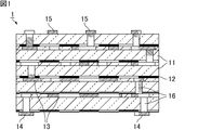
- FIG. 1 is a cross-sectional view schematically showing a multilayer ceramic substrate according to an embodiment of the ceramic electronic component of the present invention.
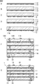
- 2A to 2G are cross-sectional views schematically showing an example of a method for manufacturing the multilayer ceramic substrate shown in FIG. 3A is a cross-sectional view schematically illustrating the multilayer ceramic substrate of Example 1, and
- FIG. 3B schematically illustrates the internal conductor layer formed on the multilayer ceramic substrate of Example 1. It is a top view. 4 is a scanning electron micrograph showing a cross section of the multilayer ceramic substrate of Example 1.
- FIG. 1 is a cross-sectional view schematically showing a multilayer ceramic substrate according to an embodiment of the ceramic electronic component of the present invention.
- 2A to 2G are cross-sectional views schematically showing an example of a method for manufacturing the multilayer ceramic substrate shown in FIG. 3A is a cross-sectional view schematically illustrating the multilayer ceramic substrate of Example 1, and
- FIG. 3B schematically illustrates the internal conductor layer formed on the
- the ceramic electronic component of the present invention and the method for manufacturing the ceramic electronic component will be described.
- the present invention is not limited to the following configurations, and can be applied with appropriate modifications without departing from the scope of the present invention.
- a combination of two or more of the individual desirable configurations of the present invention described below is also the present invention.
- the ceramic electronic component of the present invention is not limited to a multilayer ceramic substrate, but may be a chip component mounted on a multilayer ceramic substrate, for example, a ceramic electronic component such as a multilayer ceramic capacitor, a multilayer inductor, or a multilayer ceramic filter obtained by integrally firing these. It is possible to apply to.
- the ceramic electronic component of the present invention when the ceramic electronic component of the present invention is applied to a multilayer ceramic capacitor, the dielectric layer constituting the multilayer ceramic capacitor corresponds to the ceramic layer, and the inner layer electrode corresponds to the inner conductor layer.
- FIG. 1 is a cross-sectional view schematically showing a multilayer ceramic substrate according to an embodiment of the ceramic electronic component of the present invention.
- a multilayer ceramic substrate 1 shown in FIG. 1 includes a ceramic layer 11, a protective layer 12 disposed on one main surface of the ceramic layer 11, and an internal conductor layer 13 disposed on one main surface of the protective layer 12.
- a plurality of structures provided in order are stacked.
- the main surface on the lower side of the paper is one main surface
- the main surface on the upper side of the paper is the other main surface.
- the protective layer 12 and the inner conductor layer 13 are both formed substantially parallel to the ceramic layer 11.
- the internal conductor layer 13 is disposed between the ceramic layer 11 and the protective layer 12 as a wiring conductor.
- a ceramic layer having the same thickness as the internal conductor layer 13 is formed in a portion where the internal conductor layer 13 between the ceramic layer 11 and the protective layer 12 is not formed.
- the multilayer ceramic substrate 1 includes, as wiring conductors other than the internal conductor layer 13, an external conductor layer 14 disposed on one main surface of the protective layer 12 constituting one main surface of the multilayer ceramic substrate 1, and the other of the multilayer ceramic substrate 1.
- the external conductor layer 15 disposed on the other main surface of the ceramic layer 11 constituting the main surface is electrically connected to any of the internal conductor layer 13, the external conductor layer 14, and the external conductor layer 15, and the ceramic layer 11 is And a via-hole conductor 16 provided so as to penetrate in the thickness direction.
- a chip component is mounted on the other main surface of the multilayer ceramic substrate 1 while being electrically connected to the external conductor layer 15.
- the outer conductor layer 14 disposed on one main surface of the multilayer ceramic substrate 1 is used as an electrical connection means when the multilayer ceramic substrate 1 on which chip components are mounted is mounted on a motherboard.
- the ceramic layer constituting the multilayer ceramic substrate preferably contains a low-temperature sintered ceramic material.
- the low-temperature sintered ceramic material means a material that can be sintered at a firing temperature of 1000 ° C. or less and can be co-fired with copper or silver among ceramic materials.
- Examples of the low-temperature sintered ceramic material contained in the ceramic layer include a glass composite low-temperature sintered ceramic material obtained by mixing borosilicate glass with a ceramic material such as quartz, alumina, and forsterite, ZnO—MgO—Al 2 Crystallized glass-based low-temperature sintered ceramic materials using O 3 —SiO 2 -based crystallized glass, BaO—Al 2 O 3 —SiO 2 based ceramic materials and Al 2 O 3 —CaO—SiO 2 —MgO—B 2
- Non-glass type low-temperature sintered ceramic material using O 3 type ceramic material or the like can be used.
- a ceramic layer is not specifically limited, 1 micrometer or more and 60 micrometers or less are preferable.
- the protective layer is disposed between the ceramic layer and the inner conductor layer. Since the protective layer is a layer for protecting the ceramic layer, the protective layer is preferably formed on the entire surface of one main surface of the ceramic layer. Moreover, it is preferable that the protective layer is arrange
- the protective layer is made of a metal oxide and is also an insulating layer.
- the metal oxide composing the protective layer may be one in which the metal oxide or the metal before the metal oxide is oxidized is not etched with an etching solution for etching the metal foil that becomes the inner conductor layer.
- etching solution for etching the metal foil that becomes the inner conductor layer.
- titanium oxide, chromium oxide, tungsten oxide, nickel oxide, silicon oxide and the like can be mentioned.
- the protective layer may be two or more layers, but is preferably composed of one layer.
- the protective layer is mainly composed of any one metal oxide selected from the group consisting of titanium oxide, chromium oxide, tungsten oxide, nickel oxide and silicon oxide.
- the main component here means an element having a concentration of 1% by weight or more among elements of Group 1 to Group 12 detected when composition analysis is performed using inductively coupled plasma emission spectroscopy. It is an oxide containing.
- the protective layer is preferably formed by oxidizing any one metal selected from the group consisting of titanium, chromium, tungsten, and nickel. In this way, when the protective layer is formed by oxidizing the metal, a part of oxygen is supplied from the ceramic layer to the protective layer, so that the amount of oxidation of the protective layer on the inner conductor layer side is on the ceramic layer side. Less than the oxidation amount of the protective layer.
- the metal oxide constituting the protective layer is preferably also included in the ceramic layer. That is, the ceramic layer preferably contains the same metal oxide as the metal oxide constituting the protective layer, and is specifically selected from the group consisting of titanium oxide, chromium oxide, tungsten oxide, nickel oxide and silicon oxide. It is preferable that any one of these is included.
- the ceramic layer preferably contains titanium oxide.
- the thickness of a protective layer is not specifically limited, It is preferable that a protective layer is thinner than an internal conductor layer. Furthermore, the protective layer is preferably thinner than the ceramic layer. Specifically, the thickness of the protective layer is preferably 10 nm or more, more preferably 50 nm or more, further preferably 75 nm or more, and particularly preferably 100 nm or more. Further, the thickness of the protective layer is preferably 5000 nm or less, more preferably 1000 nm or less, further preferably 750 nm or less, and particularly preferably 500 nm or less.
- the inner conductor layer is formed by etching a metal foil.
- the metal contained in the inner conductor layer is preferably copper. Since copper has a low resistance, it is particularly suitable when the ceramic electronic component is used for high frequency.
- the inner conductor layer formed by etching metal foil has a higher proportion of metal contained in the inner conductor layer than the inner conductor layer formed using the conductive paste. Lower.
- the ratio of the metal contained in the inner conductor layer is preferably 90% by weight or more, more preferably 95% by weight or more, further preferably 98% by weight or more, particularly preferably 99% by weight or more, and most preferably 100% by weight.
- the thickness of the inner conductor layer is not particularly limited, but is preferably 1 ⁇ m or more, more preferably 5 ⁇ m or more, further preferably 10 ⁇ m or more, more preferably 40 ⁇ m or less, and more preferably 35 ⁇ m or less.
- the thickness of the ceramic layer, the thickness of the protective layer, and the thickness of the internal conductor layer are all measured by observing a cross section substantially perpendicular to the main surface using a scanning electron microscope (SEM).
- the inner conductor layer is preferably made of copper
- the protective layer is preferably made of titanium oxide
- the protective layer is more preferably composed mainly of titanium oxide.
- the oxidation amount of the protective layer on the inner conductor layer side is preferably smaller than the oxidation amount of the protective layer on the ceramic layer side. That is, if the composition of titanium oxide constituting the protective layer on the inner conductor layer side is TiOx and the composition of titanium oxide constituting the protective layer on the ceramic layer side is TiOy, x ⁇ y is preferable.
- the external conductor layer when the external conductor layer is disposed on one main surface of the protective layer constituting one main surface of the multilayer ceramic substrate, like the external conductor layer 14 in FIG.
- the external conductor layer may be formed using a conductive paste, it is preferably formed by etching a metal foil in the same manner as the internal conductor layer.
- the outer conductor layer disposed on one main surface of the multilayer ceramic substrate may be formed using a conductive paste without providing a protective layer.
- the external conductor layer is disposed on the other main surface of the ceramic layer constituting the other main surface of the multilayer ceramic substrate as in the case of the outer conductor layer 15 in FIG. It is preferable to form by using.
- the via-hole conductor is preferably formed using a conductive paste.
- these external conductor layer and / or via-hole conductor are preferably mainly composed of copper, silver or platinum, and copper is the main component. More preferably.
- the multilayer ceramic substrate 1 shown in FIG. 1 is preferably manufactured as follows.
- 2A to 2G are cross-sectional views schematically showing an example of a method for manufacturing the multilayer ceramic substrate shown in FIG.
- a green sheet protective layer 112 made of metal or metal oxide is formed on one main surface of the metal foil 113.
- the main surface on the upper side of the paper is one main surface.
- the green sheet protective layer 112 is preferably formed on the entire main surface of the metal foil 113.
- metal foil it is preferable to use a copper foil as the metal foil.
- the thickness of metal foil is not specifically limited, 1 micrometer or more is preferable, 5 micrometers or more are more preferable, 10 micrometers or more are further more preferable, 40 micrometers or less are preferable, and 35 micrometers or less are more preferable.
- the metal or metal oxide constituting the green sheet protective layer is not particularly limited as long as it is not etched with an etching solution for etching the metal foil, for example, metals such as titanium, chromium, tungsten and nickel, and Examples thereof include metal oxides such as silicon oxide. Metal oxides such as titanium oxide, chromium oxide, tungsten oxide and nickel oxide may be used.
- the green sheet protective layer may be two or more layers, but is preferably composed of one layer.
- the green sheet protective layer is preferably a metal layer made of any one metal selected from the group consisting of titanium, chromium, tungsten and nickel.
- the green sheet protective layer is preferably a metal oxide layer made of silicon oxide.
- the green sheet protective layer is formed by a method such as a physical vapor deposition method (PVD method) such as sputtering or vacuum deposition, a chemical vapor deposition method (CVD method) such as plasma CVD, or a plating method.
- PVD method physical vapor deposition method
- CVD method chemical vapor deposition method
- plating method a plating method.
- the metal oxide layer made of silicon oxide can also be formed by wet coating such as a sol-gel method.
- the thickness of the green sheet protective layer is not particularly limited, but the green sheet protective layer is preferably thinner than the metal foil. Furthermore, the green sheet protective layer is preferably thinner than the green sheet. Specifically, the thickness of the green sheet protective layer is preferably 10 nm or more, more preferably 50 nm or more, further preferably 75 nm or more, and particularly preferably 100 nm or more. Further, the thickness of the protective layer is preferably 5000 nm or less, more preferably 1000 nm or less, further preferably 750 nm or less, and particularly preferably 500 nm or less.
- a green sheet 111 to be the ceramic layer 11 is formed on one main surface of the green sheet protective layer 112.
- the green sheet protective layer 112 is not formed on the metal foil 113, it is preferable not to mold the green sheet 111 on the exposed metal foil 113.
- the green sheet can be formed into a sheet shape by a doctor blade method or the like, for example, a ceramic slurry containing a ceramic raw material powder such as a low-temperature sintered ceramic material, an organic binder and a solvent.
- the ceramic slurry may contain various additives such as a dispersant and a plasticizer.
- Examples of the organic binder contained in the ceramic slurry include butyral resin (polyvinyl butyral), acrylic resin, and methacrylic resin.
- the solvent for example, alcohol such as toluene and isopropyl alcohol can be used.
- the plasticizer for example, di-n-butyl phthalate can be used.
- the green sheet preferably contains a metal oxide containing the same metal element as the metal element contained in the green sheet protective layer, specifically, a group consisting of titanium oxide, chromium oxide, tungsten oxide, nickel oxide and silicon oxide. It is preferable to include any one selected from more.
- the metal foil 113 on the green sheet protective layer 112 is etched to form the inner conductor layer 13 having a conductor pattern, as shown in FIG. 2C.
- the metal foil is etched using an etchant.
- the internal conductor layer having a conductor pattern can be formed by removing the resist.
- etching solution examples include ferric chloride solution, cupric chloride solution, hydrochloric acid, sulfuric acid-hydrogen peroxide aqueous solution, persulfate aqueous solution such as ammonium persulfate, and the like. Of these, ferric chloride solutions are preferred.
- the step formed by the etching it is preferable to fill the step formed by the etching by pouring the ceramic slurry 121 used for forming the green sheet into the portion where the internal conductor layer 13 is not formed.
- holes for the via-hole conductor 16 are formed in the green sheet 111 and the green sheet protective layer 112 as shown in FIG. 2E.
- the hole may reach the inner conductor layer 13.
- a conductive paste such as a copper paste
- a conductive paste body 116 to be the via-hole conductor 16 is formed.
- the order of the step of filling the step and the step of forming the conductive paste body may be reversed.
- positioned at the main surface of a ceramic layer are formed with respect to a specific green sheet.
- the outer conductor layer 14 disposed on the main surface of the protective layer is preferably formed by etching a metal foil, similarly to the formation of the inner conductor layer 13 shown in FIGS. 2A to 2C.
- the external conductor layer 15 disposed on the main surface of the ceramic layer is preferably formed from a conductive paste layer 115 using a conductive paste.
- the external conductor layer 14 may be formed using a conductive paste without providing the green sheet protective layer.
- a green laminate 100 is obtained by laminating and pressing a plurality of green sheets including the green sheet 111 on which the green sheet protective layer 112 and the internal conductor layer 13 are formed.
- the raw laminate 100 is fired. Thereby, the green sheet is sintered into a ceramic layer. During firing, the green sheet shrinks mainly in the thickness direction.
- the green sheet protective layer becomes a protective layer made of a metal oxide by firing.
- a titanium layer is formed as the green sheet protective layer
- titanium is oxidized at the firing temperature to form a protective layer made of titanium oxide.
- the protective layer is formed by oxidizing the metal
- a part of oxygen is supplied from the ceramic layer to the protective layer, so that the amount of oxidation of the protective layer on the inner conductor layer side is on the ceramic layer side.
- a silicon oxide layer is formed as a green sheet protective layer, the metal oxide remains unchanged after firing and becomes a protective layer made of silicon oxide.
- the ceramic layer 11, the protective layer 12 disposed on one main surface of the ceramic layer 11, and the internal conductor layer 13 disposed on one main surface of the protective layer 12 are A multilayer ceramic substrate 1 in which a plurality of structures provided in order is laminated is obtained.
- the firing atmosphere is not particularly limited, but firing is preferably performed in a low oxygen atmosphere.
- the low oxygen atmosphere means an atmosphere having a lower oxygen partial pressure than the atmosphere.
- an inert gas atmosphere such as a nitrogen atmosphere or an argon atmosphere
- an atmosphere mixed with an inert gas such as nitrogen, a vacuum atmosphere, etc.
- a mixed gas atmosphere of nitrogen and hydrogen may be used.
- the constraining green sheet does not sinter substantially at the time of firing, so that the shrinkage does not occur and acts on the raw laminate to suppress the shrinkage in the main surface direction.
- the dimensional accuracy of the multilayer ceramic substrate can be increased.
- the oxidation amount of the protective layer on the inner conductor layer side is preferably smaller than the oxidation amount of the protective layer on the ceramic layer side.
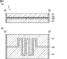
- Example 1 3A is a cross-sectional view schematically illustrating the multilayer ceramic substrate of Example 1, and FIG. 3B schematically illustrates the internal conductor layer formed on the multilayer ceramic substrate of Example 1. It is a top view.
- the multilayer ceramic substrate 2 on which the internal conductor layer 23 shown in FIGS. 3A and 3B was formed was manufactured by the following method.
- a titanium (Ti) layer having a thickness of 500 nm was formed as a green sheet protective layer on one main surface of a 10 ⁇ m thick copper (Cu) foil by sputtering.
- SiO 2 , Ba 2 CO 3 , Al 2 O 3 , TiO 2 and ZrO 2 are weighed so that the total amount is 100 g at a weight ratio of 52: 35: 10: 2: 1, 100 g of water, 5 mm in diameter Together with 500 g of the zirconia balls, was put in a polyethylene pot having an internal volume of 500 cm 3 . After mixing at 150 rpm for 16 hours, a ceramic mixed powder was prepared by drying with a spray dryer, and further heat treated at 750 ° C. for 1 hour to obtain a calcined ceramic powder.
- the obtained ceramic calcined powder, butyral resin, dioctyl phthalate, toluene, and ethanol were weighed so as to have a weight ratio of 44: 10: 2: 31: 13, and an internal volume of 500 cm 3 together with 500 g of zirconia balls having a diameter of 5 mm.
- a ceramic slurry was prepared by mixing and pulverizing at 150 rpm for 16 hours. The prepared ceramic slurry is applied by a doctor blade method to the surface on which the titanium layer of the copper foil having a thickness of 10 ⁇ m is formed so that the thickness after drying becomes 40 ⁇ m, and dried to obtain a green sheet with copper foil.
- a resist having a predetermined pattern was formed on the copper foil of the green sheet with copper foil. Thereafter, the copper foil was etched using a ferric chloride solution as an etching solution. At this time, only the copper foil surface was etched so that the green sheet was not exposed to the etching solution. After etching, the resist was removed to produce a green sheet on which an internal conductor layer having a conductor pattern was formed. As a result, an internal conductor layer having a width of 100 ⁇ m and a wiring length of 50 mm could be formed for measuring electrical resistivity after firing (see FIG. 3B).
- a plurality of green sheets including a green sheet on which an internal conductor layer was formed was laminated and pressed at 50 MPa by an isostatic press to produce a raw laminate. At this time, the thickness of the raw laminate was adjusted to 500 ⁇ m.
- the step produced by the etching was filled by pouring the ceramic slurry into the green sheets on which the internal conductor layers were formed.
- the raw laminate was fired in a low oxygen atmosphere with an oxygen partial pressure of 1.0 ⁇ 10 ⁇ 11 Pa at a top temperature of 990 ° C. and a keep time of 30 minutes.
- the heating rate was 2 ° C./min
- the cooling rate was 5 ° C./min.
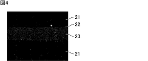
- FIG. 4 is a scanning electron micrograph showing a cross section of the multilayer ceramic substrate of Example 1.
- FIG. 4 it can be confirmed that a protective layer 22 made of titanium oxide is formed between the ceramic layers 21 on one main surface of the inner conductor layer 23 made of copper.
- an external electrode 25 is formed on the end face of the fired multilayer ceramic substrate 2 using a copper paste so as to be connected to the internal conductor layer 23.
- the electrical resistivity of the internal conductor layer was calculated by measuring the voltage between terminals when a constant current of 1 mA was passed through the external electrode. As a result, the electrical resistivity of the inner conductor layer in Example 1 was 1.8 ⁇ 10 ⁇ 8 ⁇ ⁇ m. On the other hand, the electrical resistivity when the internal conductor layer was formed using copper paste was 2.3 ⁇ 10 ⁇ 8 ⁇ ⁇ m. From the above results, it can be confirmed that the electrical resistivity of the internal conductor layer formed by etching the copper foil is lower than the electrical resistivity of the internal conductor layer formed using the copper paste.
- Example 2 A multilayer ceramic substrate was produced in the same manner as in Example 1 except that a silicon oxide (SiO 2 ) layer was formed on one main surface of the copper foil instead of the titanium layer as the green sheet protective layer. As a result, as in Example 1, an internal conductor layer having a width of 100 ⁇ m and a wiring length of 50 mm could be formed.
- SiO 2 silicon oxide
Landscapes
- Engineering & Computer Science (AREA)
- Manufacturing & Machinery (AREA)
- Microelectronics & Electronic Packaging (AREA)
- Parts Printed On Printed Circuit Boards (AREA)
- Production Of Multi-Layered Print Wiring Board (AREA)
Abstract
本発明のセラミック電子部品は、セラミック層と、上記セラミック層を保護するために上記セラミック層の一方主面に配置された、金属酸化物からなる保護層と、上記保護層の一方主面に配置された内部導体層と、をこの順に備える構造が複数積層されてなることを特徴とする。
Description
本発明は、セラミック電子部品及びセラミック電子部品の製造方法に関する。
多層セラミック基板及び積層セラミックコンデンサ等のセラミック電子部品は、通常、セラミック層となるグリーンシートを基材フィルム上に成形した後、導電性ペーストをスクリーン印刷する等してグリーンシート上に導体パターンを形成し、次いで、導体パターンが形成されたグリーンシートを複数枚積層して生の積層体を形成し、この生の積層体を焼成することにより得られる(例えば、特許文献1及び2参照)。
セラミック電子部品の従来の製造方法では、導電性ペーストを用いて導体パターンを形成するため、印刷精度が制約となり、微細な導体パターンを有する内部導体層を形成することが困難であるという問題があった。
本発明は上記の問題を解決するためになされたものであり、微細な導体パターンを有する内部導体層が形成されたセラミック電子部品、及び、該セラミック電子部品の製造方法を提供することを目的とする。
本発明者らは、セラミック層となるグリーンシートを金属箔上に成形し、この金属箔をエッチングすることにより、微細な導体パターンを有する内部導体層を形成することができるのではないかと考えた。しかし、金属箔のエッチングに用いられるエッチング液にグリーンシートが曝されると、グリーンシートが形状を保てなくなってしまう。そこで、本発明者らは、グリーンシートをエッチングから保護するための保護層を金属箔の一方主面に形成しておき、この保護層上にグリーンシートを成形した後で金属箔をエッチングする方法を考え、本発明を完成した。
本発明のセラミック電子部品は、セラミック層と、上記セラミック層を保護するために上記セラミック層の一方主面に配置された、金属酸化物からなる保護層と、上記保護層の一方主面に配置された内部導体層と、をこの順に備える構造が複数積層されてなることを特徴とする。
本発明のセラミック電子部品は、後述するように、グリーンシート保護層及び内部導体層が形成されたグリーンシートを含む複数のグリーンシートを積層して生の積層体を得て、この生の積層体を焼成することにより製造される。そのため、焼成後のセラミック電子部品においては、セラミック層と内部導体層との間に、金属酸化物からなる保護層が残留する。さらに、本発明のセラミック電子部品を製造する際には、金属箔のエッチングによって内部導体層を形成するため、導電性ペーストを用いて内部導体層を形成する場合に比べて、導体パターンを微細かつ高密度にすることができ、さらには、内部導体層の電気抵抗率を低くすることができる。また、肉厚の金属箔を用いれば、セラミック層に対して厚い内部導体層を形成することもできるため、大電流が流れる場合の発熱が少なく、放熱性が高いセラミック電子部品とすることができる。
本発明のセラミック電子部品において、上記保護層は、酸化チタン、酸化クロム、酸化タングステン、酸化ニッケル及び酸化ケイ素からなる群より選択されるいずれか1種の金属酸化物を主成分とすることが好ましい。
上記保護層は、上記金属酸化物、又は、上記の金属酸化物が酸化される前の金属からなるグリーンシート保護層から形成されるものである。後述するように、上記金属酸化物、又は、上記の金属酸化物が酸化される前の金属は、グリーンシートをエッチングから保護する材料として好適に用いることができる。
上記保護層は、上記金属酸化物、又は、上記の金属酸化物が酸化される前の金属からなるグリーンシート保護層から形成されるものである。後述するように、上記金属酸化物、又は、上記の金属酸化物が酸化される前の金属は、グリーンシートをエッチングから保護する材料として好適に用いることができる。
本発明のセラミック電子部品において、上記保護層を構成する上記金属酸化物は、上記セラミック層にも含まれることが好ましい。
保護層とセラミック層とが同じ金属酸化物を含んでいると、焼成時の熱膨張や熱収縮の差が緩和されるため、焼成を行いやすく、また、焼成後の基板割れも生じ難くなる。
保護層とセラミック層とが同じ金属酸化物を含んでいると、焼成時の熱膨張や熱収縮の差が緩和されるため、焼成を行いやすく、また、焼成後の基板割れも生じ難くなる。
本発明のセラミック電子部品において、上記保護層は、上記内部導体層より薄いことが好ましい。さらに、上記保護層は、上記セラミック層より薄いことが好ましい。
保護層を薄くすることにより、セラミック電子部品を小型化することができるだけでなく、保護層によって電気特性を損なうことなく、高機能なセラミック電子部品を作製することができる。
保護層を薄くすることにより、セラミック電子部品を小型化することができるだけでなく、保護層によって電気特性を損なうことなく、高機能なセラミック電子部品を作製することができる。
本発明のセラミック電子部品において、上記内部導体層は、銅からなり、上記保護層は、酸化チタンからなることが好ましい。
後述の製造方法では、酸化チタンからなる保護層は、チタン層が焼成時に酸化されることによって形成される。銅とチタンとは密着性が高いため、セラミック電子部品を製造する際の焼成時に、内部導体層と保護層との間に不所望な空隙が形成されることを抑制することができる。
後述の製造方法では、酸化チタンからなる保護層は、チタン層が焼成時に酸化されることによって形成される。銅とチタンとは密着性が高いため、セラミック電子部品を製造する際の焼成時に、内部導体層と保護層との間に不所望な空隙が形成されることを抑制することができる。
本発明のセラミック電子部品の製造方法は、金属箔の一方主面に、金属又は金属酸化物からなるグリーンシート保護層を形成する工程と、上記グリーンシート保護層の一方主面に、セラミック層となるグリーンシートを成形する工程と、上記グリーンシート保護層上の上記金属箔をエッチングすることにより、導体パターンを有する内部導体層を形成する工程と、上記グリーンシート保護層及び上記内部導体層が形成された上記グリーンシートを含む複数のグリーンシートを積層及び圧着することにより、生の積層体を得る工程と、上記生の積層体を焼成する工程と、を備え、上記グリーンシート保護層は、上記金属箔をエッチングする工程においては、エッチングされずに上記グリーンシートをエッチングから保護し、かつ、上記生の積層体を焼成する工程の後には、金属酸化物からなる保護層となることを特徴とする。
本発明のセラミック電子部品の製造方法では、金属又は金属酸化物からなるグリーンシート保護層を金属箔の一方主面に形成し、グリーンシート保護層上にグリーンシートを成形した後、グリーンシート保護層上の金属箔をエッチングする。金属箔をエッチングする工程においてエッチングされないグリーンシート保護層を金属箔上に形成しておくことにより、グリーンシートをエッチングから保護することができる。さらに、金属箔のエッチングによって内部導体層を形成することにより、導電性ペーストを用いて内部導体層を形成する場合に比べて、導体パターンを微細かつ高密度にすることができ、さらには、内部導体層の電気抵抗率を低くすることができる。また、肉厚の金属箔を用いれば、セラミック層に対して厚い内部導体層を形成することもできるため、大電流が流れる場合の発熱が少なく、放熱性が高いセラミック電子部品とすることができる。
本発明のセラミック電子部品の製造方法において、上記グリーンシート保護層は、チタン、クロム、タングステン及びニッケルからなる群より選択されるいずれか1種の金属からなる金属層であることが好ましい。また、上記グリーンシート保護層は、酸化ケイ素からなる金属酸化物層であることが好ましい。
上記金属又は金属酸化物は、グリーンシートをエッチングから保護する材料として好適に用いることができる。
上記金属又は金属酸化物は、グリーンシートをエッチングから保護する材料として好適に用いることができる。
本発明のセラミック電子部品の製造方法において、上記グリーンシート保護層を形成する工程では、上記金属箔として銅箔を使用し、上記銅箔の一方主面に、上記グリーンシート保護層としてチタン層を形成することが好ましい。
銅とチタンとは密着性が高いため、セラミック電子部品を製造する際の焼成時に、内部導体層と保護層との間に不所望な空隙が形成されることを抑制することができる。
銅とチタンとは密着性が高いため、セラミック電子部品を製造する際の焼成時に、内部導体層と保護層との間に不所望な空隙が形成されることを抑制することができる。
本発明によれば、微細な導体パターンを有する内部導体層が形成されたセラミック電子部品、及び、該セラミック電子部品の製造方法を提供することができる。
以下、本発明のセラミック電子部品及びセラミック電子部品の製造方法について説明する。
しかしながら、本発明は、以下の構成に限定されるものではなく、本発明の要旨を変更しない範囲において適宜変更して適用することができる。
以下において記載する本発明の個々の望ましい構成を2つ以上組み合わせたものもまた本発明である。
しかしながら、本発明は、以下の構成に限定されるものではなく、本発明の要旨を変更しない範囲において適宜変更して適用することができる。
以下において記載する本発明の個々の望ましい構成を2つ以上組み合わせたものもまた本発明である。
本発明のセラミック電子部品の一実施形態として、多層セラミック基板を例にとって説明する。
しかし、本発明のセラミック電子部品は、多層セラミック基板に限らず、多層セラミック基板に搭載するチップ部品、例えば、積層セラミックコンデンサ、積層インダクタ、あるいはこれらを一体焼成した積層セラミックフィルタ等のセラミック電子部品に対して適用することが可能である。例えば、本発明のセラミック電子部品を積層セラミックコンデンサに適用する場合、積層セラミックコンデンサを構成する誘電体層がセラミック層に、内層電極が内部導体層に該当する。
しかし、本発明のセラミック電子部品は、多層セラミック基板に限らず、多層セラミック基板に搭載するチップ部品、例えば、積層セラミックコンデンサ、積層インダクタ、あるいはこれらを一体焼成した積層セラミックフィルタ等のセラミック電子部品に対して適用することが可能である。例えば、本発明のセラミック電子部品を積層セラミックコンデンサに適用する場合、積層セラミックコンデンサを構成する誘電体層がセラミック層に、内層電極が内部導体層に該当する。
図1は、本発明のセラミック電子部品の一実施形態に係る多層セラミック基板を模式的に示す断面図である。
図1に示す多層セラミック基板1は、セラミック層11と、セラミック層11の一方主面に配置された保護層12と、保護層12の一方主面に配置された内部導体層13と、をこの順に備える構造が複数積層されてなる。図1では、紙面下側の主面が一方主面であり、紙面上側の主面が他方主面である。保護層12及び内部導体層13は、いずれも、セラミック層11に実質的に平行に形成されている。
図1に示す多層セラミック基板1は、セラミック層11と、セラミック層11の一方主面に配置された保護層12と、保護層12の一方主面に配置された内部導体層13と、をこの順に備える構造が複数積層されてなる。図1では、紙面下側の主面が一方主面であり、紙面上側の主面が他方主面である。保護層12及び内部導体層13は、いずれも、セラミック層11に実質的に平行に形成されている。
内部導体層13は、配線導体として、セラミック層11と保護層12との間に配置されている。セラミック層11と保護層12との間の内部導体層13が形成されていない部分には、内部導体層13と同じ厚みのセラミック層が形成されている。
多層セラミック基板1は、内部導体層13以外の配線導体として、多層セラミック基板1の一方主面を構成する保護層12の一方主面に配置された外部導体層14と、多層セラミック基板1の他方主面を構成するセラミック層11の他方主面に配置された外部導体層15と、内部導体層13、外部導体層14及び外部導体層15のいずれかと電気的に接続され、かつセラミック層11を厚み方向に貫通するように設けられたビアホール導体16と、を備えている。
例えば、多層セラミック基板1の他方主面上には、外部導体層15に電気的に接続された状態で、チップ部品が搭載される。多層セラミック基板1の一方主面に配置された外部導体層14は、チップ部品が搭載された多層セラミック基板1をマザーボード上に実装する際の電気的接続手段として用いられる。
本発明のセラミック電子部品において、多層セラミック基板を構成するセラミック層は、低温焼結セラミック材料を含有することが好ましい。
低温焼結セラミック材料とは、セラミック材料のうち、1000℃以下の焼成温度で焼結可能であり、銅や銀との同時焼成が可能である材料を意味する。
低温焼結セラミック材料とは、セラミック材料のうち、1000℃以下の焼成温度で焼結可能であり、銅や銀との同時焼成が可能である材料を意味する。
セラミック層に含有される低温焼結セラミック材料としては、例えば、クオーツやアルミナ、フォルステライト等のセラミック材料にホウ珪酸ガラスを混合してなるガラス複合系低温焼結セラミック材料、ZnO-MgO-Al2O3-SiO2系の結晶化ガラスを用いた結晶化ガラス系低温焼結セラミック材料、BaO-Al2O3-SiO2系セラミック材料やAl2O3-CaO-SiO2-MgO-B2O3系セラミック材料等を用いた非ガラス系低温焼結セラミック材料等が挙げられる。
セラミック層の厚みは特に限定されないが、1μm以上、60μm以下が好ましい。
本発明のセラミック電子部品において、保護層は、セラミック層と内部導体層との間に配置されている。保護層は、セラミック層を保護するための層であるため、セラミック層の一方主面の全面に形成されていることが好ましい。また、保護層は、内部導体層が形成されたすべてのセラミック層の一方主面に配置されていることが好ましい。
保護層は、金属酸化物からなり、絶縁層でもある。保護層を構成する金属酸化物は、当該金属酸化物、又は、当該金属酸化物が酸化される前の金属が、内部導体層となる金属箔をエッチングするためのエッチング液でエッチングされないものであれば特に限定されず、例えば、酸化チタン、酸化クロム、酸化タングステン、酸化ニッケル及び酸化ケイ素等が挙げられる。保護層は、2層以上でもよいが、1層からなることが好ましい。
保護層は、酸化チタン、酸化クロム、酸化タングステン、酸化ニッケル及び酸化ケイ素からなる群より選択されるいずれか1種の金属酸化物を主成分とすることがより好ましい。
なお、ここでいう主成分とは、誘導結合プラズマ発光分光法を用いて組成分析を行った際に検出される第1族~第12族元素のうち、含有濃度が1重量%以上の元素を含む酸化物のことである。
なお、ここでいう主成分とは、誘導結合プラズマ発光分光法を用いて組成分析を行った際に検出される第1族~第12族元素のうち、含有濃度が1重量%以上の元素を含む酸化物のことである。
本発明のセラミック電子部品において、上記保護層は、チタン、クロム、タングステン及びニッケルからなる群より選択されるいずれか1種の金属が酸化されることによって形成されることが好ましい。このように、金属が酸化されることによって保護層が形成される場合、セラミック層から一部の酸素が保護層に供給されるため、内部導体層側の保護層の酸化量がセラミック層側の保護層の酸化量よりも少なくなる。
本発明のセラミック電子部品において、保護層を構成する上記金属酸化物は、セラミック層にも含まれることが好ましい。すなわち、セラミック層は、保護層を構成する金属酸化物と同じ金属酸化物を含むことが好ましく、具体的には、酸化チタン、酸化クロム、酸化タングステン、酸化ニッケル及び酸化ケイ素からなる群より選択されるいずれか1種を含むことが好ましい。例えば、保護層が酸化チタンからなる場合、セラミック層が酸化チタンを含むことが好ましい。
保護層の厚みは特に限定されないが、保護層は、内部導体層より薄いことが好ましい。さらに、保護層は、セラミック層より薄いことが好ましい。
具体的には、保護層の厚みは、10nm以上が好ましく、50nm以上がより好ましく、75nm以上がさらに好ましく、100nm以上が特に好ましい。また、保護層の厚みは、5000nm以下が好ましく、1000nm以下がより好ましく、750nm以下がさらに好ましく、500nm以下が特に好ましい。
具体的には、保護層の厚みは、10nm以上が好ましく、50nm以上がより好ましく、75nm以上がさらに好ましく、100nm以上が特に好ましい。また、保護層の厚みは、5000nm以下が好ましく、1000nm以下がより好ましく、750nm以下がさらに好ましく、500nm以下が特に好ましい。
本発明のセラミック電子部品において、内部導体層は、金属箔のエッチングによって形成される。内部導体層に含まれる金属は、銅であることが好ましい。銅は低抵抗であるため、特に、セラミック電子部品が高周波用途である場合に適している。
金属箔のエッチングによって形成される内部導体層では、導電性ペーストを用いて形成される内部導体層に比べて、内部導体層に含まれる金属の割合が多いため、内部導体層の電気抵抗率が低くなる。内部導体層に含まれる金属の割合は、90重量%以上が好ましく、95重量%以上がより好ましく、98重量%以上がさらに好ましく、99重量%以上が特に好ましく、100重量%が最も好ましい。
内部導体層の厚みは特に限定されないが、1μm以上が好ましく、5μm以上がより好ましく、10μm以上がさらに好ましく、また、40μm以下が好ましく、35μm以下がより好ましい。
なお、セラミック層の厚み、保護層の厚み、及び、内部導体層の厚みは、いずれも、走査型電子顕微鏡(SEM)を用いた主面に略垂直な断面の観察により測定される。
本発明のセラミック電子部品においては、特に、内部導体層が銅からなり、保護層が酸化チタンからなることが好ましく、保護層が酸化チタンを主成分とすることがより好ましい。この場合、内部導体層側の保護層の酸化量がセラミック層側の保護層の酸化量よりも少ないことが好ましい。すなわち、内部導体層側の保護層を構成する酸化チタンの組成をTiOx、セラミック層側の保護層を構成する酸化チタンの組成をTiOyとすると、x<yであることが好ましい。
本発明のセラミック電子部品において、図1中の外部導体層14のように、多層セラミック基板の一方主面を構成する保護層の一方主面に外部導体層が配置される場合、この外部導体層は、導電性ペーストを用いて形成されてもよいが、内部導体層と同様に、金属箔のエッチングによって形成されることが好ましい。ただし、多層セラミック基板の一方主面に配置される外部導体層は、保護層が設けられずに、導電性ペーストを用いて形成されてもよい。
一方、図1中の外部導体層15のように、多層セラミック基板の他方主面を構成するセラミック層の他方主面に外部導体層が配置される場合、この外部導体層は、導電性ペーストを用いて形成されることが好ましい。また、ビアホール導体が設けられる場合、ビアホール導体は、導電性ペーストを用いて形成されることが好ましい。導電性ペーストを用いて外部導体層及び/又はビアホール導体が形成される場合、これらの外部導体層及び/又はビアホール導体は、銅、銀又は白金を主成分とすることが好ましく、銅を主成分とすることがより好ましい。
図1に示す多層セラミック基板1は、好ましくは、以下のように製造される。
図2A~図2Gは、図1に示す多層セラミック基板の製造方法の一例を模式的に示す断面図である。
図2A~図2Gは、図1に示す多層セラミック基板の製造方法の一例を模式的に示す断面図である。
まず、図2Aに示すように、金属箔113の一方主面に、金属又は金属酸化物からなるグリーンシート保護層112を形成する。図2Aでは、紙面上側の主面が一方主面である。グリーンシート保護層112は、金属箔113の一方主面の全面に形成されることが好ましい。
金属箔としては、銅箔を用いることが好ましい。金属箔の厚みは特に限定されないが、1μm以上が好ましく、5μm以上がより好ましく、10μm以上がさらに好ましく、また、40μm以下が好ましく、35μm以下がより好ましい。
グリーンシート保護層を構成する金属又は金属酸化物は、金属箔をエッチングするためのエッチング液でエッチングされないものであれば特に限定されず、例えば、チタン、クロム、タングステン及びニッケル等の金属、並びに、酸化ケイ素等の金属酸化物が挙げられる。酸化チタン、酸化クロム、酸化タングステン及び酸化ニッケル等の金属酸化物であってもよい。グリーンシート保護層は、2層以上でもよいが、1層からなることが好ましい。
グリーンシート保護層は、チタン、クロム、タングステン及びニッケルからなる群より選択されるいずれか1種の金属からなる金属層であることが好ましい。また、グリーンシート保護層は、酸化ケイ素からなる金属酸化物層であることが好ましい。
グリーンシート保護層は、例えば、スパッタ法や真空蒸着法等の物理的気相成長法(PVD法)、プラズマCVD等の化学的気相成長法(CVD法)、めっき法等の方法によって形成することができる。また、酸化ケイ素からなる金属酸化物層は、上記の方法に加えて、ゾルゲル法等の湿式コーティングによって形成することもできる。
グリーンシート保護層の厚みは特に限定されないが、グリーンシート保護層は、金属箔より薄いことが好ましい。さらに、グリーンシート保護層は、グリーンシートより薄いことが好ましい。
具体的には、グリーンシート保護層の厚みは、10nm以上が好ましく、50nm以上がより好ましく、75nm以上がさらに好ましく、100nm以上が特に好ましい。また、保護層の厚みは、5000nm以下が好ましく、1000nm以下がより好ましく、750nm以下がさらに好ましく、500nm以下が特に好ましい。
具体的には、グリーンシート保護層の厚みは、10nm以上が好ましく、50nm以上がより好ましく、75nm以上がさらに好ましく、100nm以上が特に好ましい。また、保護層の厚みは、5000nm以下が好ましく、1000nm以下がより好ましく、750nm以下がさらに好ましく、500nm以下が特に好ましい。
次に、図2Bに示すように、グリーンシート保護層112の一方主面に、セラミック層11となるグリーンシート111を成形する。金属箔113上にグリーンシート保護層112が形成されていない部分が存在する場合、露出した金属箔113上にグリーンシート111を成形しないことが好ましい。
グリーンシートは、例えば低温焼結セラミック材料のようなセラミック原料の粉末と、有機バインダと溶剤とを含有するセラミックスラリーを、ドクターブレード法等によってシート状に成形することができる。上記セラミックスラリーには、分散剤、可塑剤等の種々の添加剤が含有されていてもよい。
上記セラミックスラリーに含有される有機バインダとしては、例えば、ブチラール樹脂(ポリビニルブチラール)、アクリル樹脂、メタクリル樹脂等を用いることができる。溶剤としては、例えば、トルエン、イソプロピルアルコール等のアルコール等を用いることができる。可塑剤としては、例えば、ジ-n-ブチルフタレート等を用いることができる。
グリーンシートは、グリーンシート保護層に含まれる金属元素と同じ金属元素を含む金属酸化物を含むことが好ましく、具体的には、酸化チタン、酸化クロム、酸化タングステン、酸化ニッケル及び酸化ケイ素からなる群より選択されるいずれか1種を含むことが好ましい。
続いて、グリーンシート保護層112上の金属箔113をエッチングすることにより、図2Cに示すように、導体パターンを有する内部導体層13を形成する。具体的には、金属箔に、所定のパターンを有するレジストを形成した後、エッチング液を用いて金属箔のエッチングを行う。この際、グリーンシートがエッチング液に曝されないように、金属箔面のみをエッチングすることが好ましい。グリーンシート保護層は、金属箔をエッチングするためのエッチング液ではエッチングされないため、グリーンシートをエッチングから保護することができる。エッチング後、レジストを除去することにより、導体パターンを有する内部導体層を形成することができる。
エッチング液としては、例えば、塩化第二鉄溶液、塩化第二銅溶液、塩酸、硫酸-過酸化水素水溶液、過硫酸アンモニウム等の過硫酸塩水溶液等が挙げられる。これらの中では、塩化第二鉄溶液が好ましい。
図2Dに示すように、内部導体層13が形成されていない部分に、グリーンシートを成形するために使用したセラミックスラリー121を流し込むことによって、エッチングにより生じた段差を埋めることが好ましい。
必要に応じて、図2Eに示すように、グリーンシート111及びグリーンシート保護層112に、ビアホール導体16のための孔を形成する。該孔は内部導体層13に達してもよい。該孔に、銅ペースト等の導電性ペーストを充填することによって、ビアホール導体16となる導電性ペースト体116を形成する。
なお、段差を埋める工程及び導電性ペースト体を形成する工程の順序は、逆であってもよい。
また、特定のグリーンシートに対して、保護層の主面に配置される外部導体層14、及び、セラミック層の主面に配置される外部導体層15を形成する。保護層の主面に配置される外部導体層14は、図2A~図2Cに示した内部導体層13の形成と同様に、金属箔のエッチングによって形成されることが好ましい。一方、セラミック層の主面に配置される外部導体層15は、導電性ペーストを用いた導電性ペースト層115から形成されることが好ましい。ただし、外部導体層14は、外部導体層15と同様、グリーンシート保護層を設けずに、導電性ペーストを用いて形成されてもよい。
図2Fに示すように、グリーンシート保護層112及び内部導体層13が形成されたグリーンシート111を含む複数のグリーンシートを積層及び圧着することにより、生の積層体100を得る。
その後、生の積層体100を焼成する。これにより、グリーンシートは焼結してセラミック層となる。焼成時、グリーンシートは、主に厚み方向に収縮する。
また、焼成によって、グリーンシート保護層は、金属酸化物からなる保護層となる。例えば、グリーンシート保護層としてチタン層が形成されている場合、焼成温度でチタンが酸化され、酸化チタンからなる保護層となる。このように、金属が酸化されることによって保護層が形成される場合、セラミック層から一部の酸素が保護層に供給されるため、内部導体層側の保護層の酸化量がセラミック層側の保護層の酸化量よりも少なくなる。
一方、グリーンシート保護層として酸化ケイ素層が形成されている場合、焼成後も金属酸化物のまま変化せず、酸化ケイ素からなる保護層となる。
一方、グリーンシート保護層として酸化ケイ素層が形成されている場合、焼成後も金属酸化物のまま変化せず、酸化ケイ素からなる保護層となる。
その結果、図2Gに示すように、セラミック層11と、セラミック層11の一方主面に配置された保護層12と、保護層12の一方主面に配置された内部導体層13と、をこの順に備える構造が複数積層されてなる多層セラミック基板1が得られる。
グリーンシートが低温焼結セラミック材料を含有する場合、例えば1000℃以下の焼成温度が適用される。また、焼成雰囲気は特に限定されないが、低酸素雰囲気下で焼成を行うことが好ましい。低酸素雰囲気とは、大気よりも酸素分圧が低い雰囲気を意味し、例えば、窒素雰囲気又はアルゴン雰囲気等の不活性ガス雰囲気、窒素等の不活性ガスを大気に混入した雰囲気、真空雰囲気等が挙げられる。また、窒素と水素の混合ガス雰囲気であってもよい。
なお、グリーンシートが焼結する温度では実質的に焼結しない無機材料(Al2O3等)を含有する拘束用グリーンシートを準備し、生の積層体の両主面に拘束用グリーンシートを配置した状態で生の積層体を焼成してもよい。
この場合、拘束用グリーンシートは、焼成時において実質的に焼結しないので収縮が生じず、生の積層体に対して主面方向での収縮を抑制するように作用する。その結果、多層セラミック基板の寸法精度を高めることができる。
この場合、拘束用グリーンシートは、焼成時において実質的に焼結しないので収縮が生じず、生の積層体に対して主面方向での収縮を抑制するように作用する。その結果、多層セラミック基板の寸法精度を高めることができる。
本発明のセラミック電子部品の製造方法においては、特に、金属箔として銅箔を使用し、上記銅箔の一方主面に、グリーンシート保護層としてチタン層を形成することが好ましい。この場合、内部導体層側の保護層の酸化量がセラミック層側の保護層の酸化量よりも少ないことが好ましい。
以下、本発明のセラミック電子部品及びセラミック電子部品の製造方法をより具体的に開示した実施例を示す。なお、本発明は、これらの実施例のみに限定されるものではない。
(実施例1)
図3(a)は、実施例1の多層セラミック基板を模式的に示す断面図であり、図3(b)は、実施例1の多層セラミック基板に形成された内部導体層を模式的に示す平面図である。
実施例1では、以下の方法により、図3(a)及び図3(b)に示す内部導体層23が形成された多層セラミック基板2を作製した。
図3(a)は、実施例1の多層セラミック基板を模式的に示す断面図であり、図3(b)は、実施例1の多層セラミック基板に形成された内部導体層を模式的に示す平面図である。
実施例1では、以下の方法により、図3(a)及び図3(b)に示す内部導体層23が形成された多層セラミック基板2を作製した。
厚み10μmの銅(Cu)箔の一方主面に、グリーンシート保護層として、チタン(Ti)層をスパッタ法により500nm成膜した。
SiO2、Ba2CO3、Al2O3、TiO2及びZrO2を、重量比で52:35:10:2:1の割合で総量が100gとなるように秤量し、水100g、直径5mmのジルコニアボール500gとともに内容積500cm3のポリエチレン製ポットに入れた。150rpmで16時間混合後、スプレードライヤーで乾燥することによりセラミック混合粉を作製し、さらに750℃で1時間熱処理することによりセラミック仮焼粉を得た。得られたセラミック仮焼粉、ブチラール樹脂、フタル酸ジオクチル、トルエン及びエタノールを、重量比で44:10:2:31:13となるように秤量し、直径5mmのジルコニアボール500gとともに内容積500cm3のポリエチレン製ポットに入れた。150rpmで16時間混合、粉砕することにより、セラミックスラリーを作製した。作製したセラミックスラリーを、ドクターブレード法にて、上記厚み10μmの銅箔のチタン層を成膜した面に乾燥後の厚みが40μmとなるように塗布し、乾燥させることにより、銅箔付きグリーンシートを作製した。
銅箔付きグリーンシートの銅箔に、所定のパターンを有するレジストを形成した。その後、エッチング液として塩化第二鉄溶液を用いて銅箔のエッチングを行った。この際、グリーンシートがエッチング液に曝されないように、銅箔面のみをエッチングした。エッチング後、レジストを除去することにより、導体パターンを有する内部導体層が形成されたグリーンシートを作製した。その結果、焼成後の電気抵抗率測定用として、幅100μm、配線長50mmの内部導体層を形成することができた(図3(b)参照)。
内部導体層が形成されたグリーンシートを含む複数のグリーンシートを積層し、静水圧プレスにて50MPaで圧着することにより、生の積層体を作製した。この際、生の積層体の厚みが500μmとなるようにした。なお、グリーンシートを積層する前に、内部導体層が形成されたグリーンシートに対して、上記セラミックスラリーを流し込むことによって、エッチングにより生じた段差を埋めておいた。
生の積層体を、酸素分圧1.0×10⁻¹¹Paの低酸素雰囲気下で、トップ温度990℃、キープ時間30分にて焼成した。ここで、昇温速度は2℃/分、冷却速度は5℃/分とした。
その結果、基板割れ等の欠陥のない多層セラミック基板が得られた。
その結果、基板割れ等の欠陥のない多層セラミック基板が得られた。
図4は、実施例1の多層セラミック基板の断面を示す走査型電子顕微鏡写真である。
図4に示すように、セラミック層21間には、銅からなる内部導体層23の一主面に、酸化チタンからなる保護層22が形成されていることが確認できる。
図4に示すように、セラミック層21間には、銅からなる内部導体層23の一主面に、酸化チタンからなる保護層22が形成されていることが確認できる。
また、図3(a)及び図3(b)に示すように、焼成後の多層セラミック基板2の端面に、銅ペーストを用いて、内部導体層23と接続するように外部電極25を形成した。外部電極に1mAの一定電流を流したときの端子間電圧を測定することで、内部導体層の電気抵抗率を算出した。その結果、実施例1における内部導体層の電気抵抗率は1.8×10⁻⁸Ω・mであった。一方、銅ペーストを用いて内部導体層を形成した場合の電気抵抗率は2.3×10⁻⁸Ω・mであった。以上の結果から、銅箔のエッチングによって形成された内部導体層の電気抵抗率は、銅ペーストを用いて形成された内部導体層の電気抵抗率よりも低いことが確認できる。
(実施例2)
グリーンシート保護層として、チタン層に代えて酸化ケイ素(SiO2)層を銅箔の一方主面に形成したことを除いて、実施例1と同様に多層セラミック基板を作製した。
その結果、実施例1と同様、幅100μm、配線長50mmの内部導体層を形成することができた。
グリーンシート保護層として、チタン層に代えて酸化ケイ素(SiO2)層を銅箔の一方主面に形成したことを除いて、実施例1と同様に多層セラミック基板を作製した。
その結果、実施例1と同様、幅100μm、配線長50mmの内部導体層を形成することができた。
1,2 多層セラミック基板(セラミック電子部品)
11,21 セラミック層
12,22 保護層
13,23 内部導体層
14,15 外部導体層
16 ビアホール導体
25 外部電極
100 生の積層体
111 グリーンシート
112 グリーンシート保護層
113 金属箔
115 導電性ペースト層
116 導電性ペースト体
121 セラミックスラリー
11,21 セラミック層
12,22 保護層
13,23 内部導体層
14,15 外部導体層
16 ビアホール導体
25 外部電極
100 生の積層体
111 グリーンシート
112 グリーンシート保護層
113 金属箔
115 導電性ペースト層
116 導電性ペースト体
121 セラミックスラリー
Claims (10)
- セラミック層と、
前記セラミック層を保護するために前記セラミック層の一方主面に配置された、金属酸化物からなる保護層と、
前記保護層の一方主面に配置された内部導体層と、をこの順に備える構造が複数積層されてなることを特徴とするセラミック電子部品。 - 前記保護層は、酸化チタン、酸化クロム、酸化タングステン、酸化ニッケル及び酸化ケイ素からなる群より選択されるいずれか1種の金属酸化物を主成分とする請求項1に記載のセラミック電子部品。
- 前記保護層を構成する前記金属酸化物は、前記セラミック層にも含まれる請求項1又は2に記載のセラミック電子部品。
- 前記保護層は、前記内部導体層より薄い請求項1~3のいずれかに記載のセラミック電子部品。
- 前記保護層は、前記セラミック層より薄い請求項4に記載のセラミック電子部品。
- 前記内部導体層は、銅からなり、
前記保護層は、酸化チタンからなる請求項1~5のいずれかに記載のセラミック電子部品。 - 請求項1~6のいずれかに記載のセラミック電子部品の製造方法であって、
金属箔の一方主面に、金属又は金属酸化物からなるグリーンシート保護層を形成する工程と、
前記グリーンシート保護層の一方主面に、セラミック層となるグリーンシートを成形する工程と、
前記グリーンシート保護層上の前記金属箔をエッチングすることにより、導体パターンを有する内部導体層を形成する工程と、
前記グリーンシート保護層及び前記内部導体層が形成された前記グリーンシートを含む複数のグリーンシートを積層及び圧着することにより、生の積層体を得る工程と、
前記生の積層体を焼成する工程と、を備え、
前記グリーンシート保護層は、前記金属箔をエッチングする工程においては、エッチングされずに前記グリーンシートをエッチングから保護し、かつ、前記生の積層体を焼成する工程の後には、金属酸化物からなる保護層となることを特徴とするセラミック電子部品の製造方法。 - 前記グリーンシート保護層は、チタン、クロム、タングステン及びニッケルからなる群より選択されるいずれか1種の金属からなる金属層である請求項7に記載のセラミック電子部品の製造方法。
- 前記グリーンシート保護層は、酸化ケイ素からなる金属酸化物層である請求項7に記載のセラミック電子部品の製造方法。
- 前記グリーンシート保護層を形成する工程では、
前記金属箔として銅箔を使用し、
前記銅箔の一方主面に、前記グリーンシート保護層としてチタン層を形成する請求項7に記載のセラミック電子部品の製造方法。
Applications Claiming Priority (2)
| Application Number | Priority Date | Filing Date | Title |
|---|---|---|---|
| JP2016-096448 | 2016-05-12 | ||
| JP2016096448 | 2016-05-12 |
Publications (1)
| Publication Number | Publication Date |
|---|---|
| WO2017195414A1 true WO2017195414A1 (ja) | 2017-11-16 |
Family
ID=60267038
Family Applications (1)
| Application Number | Title | Priority Date | Filing Date |
|---|---|---|---|
| PCT/JP2017/004158 Ceased WO2017195414A1 (ja) | 2016-05-12 | 2017-02-06 | セラミック電子部品及びセラミック電子部品の製造方法 |
Country Status (1)
| Country | Link |
|---|---|
| WO (1) | WO2017195414A1 (ja) |
Citations (5)
| Publication number | Priority date | Publication date | Assignee | Title |
|---|---|---|---|---|
| JPS6314493A (ja) * | 1986-07-04 | 1988-01-21 | 新光電気工業株式会社 | 多層セラミツク基板の製造方法 |
| JPH046896A (ja) * | 1990-04-24 | 1992-01-10 | World Metal:Kk | セラミック配線板 |
| JPH04260621A (ja) * | 1991-02-12 | 1992-09-16 | Minolta Camera Co Ltd | ガラス成形用金型の製作方法 |
| JPH04355086A (ja) * | 1991-03-06 | 1992-12-09 | Internatl Business Mach Corp <Ibm> | 電気接続要素の製造方法 |
| JP2004055728A (ja) * | 2002-07-18 | 2004-02-19 | Murata Mfg Co Ltd | 積層型セラミック電子部品およびその製造方法 |
-
2017
- 2017-02-06 WO PCT/JP2017/004158 patent/WO2017195414A1/ja not_active Ceased
Patent Citations (5)
| Publication number | Priority date | Publication date | Assignee | Title |
|---|---|---|---|---|
| JPS6314493A (ja) * | 1986-07-04 | 1988-01-21 | 新光電気工業株式会社 | 多層セラミツク基板の製造方法 |
| JPH046896A (ja) * | 1990-04-24 | 1992-01-10 | World Metal:Kk | セラミック配線板 |
| JPH04260621A (ja) * | 1991-02-12 | 1992-09-16 | Minolta Camera Co Ltd | ガラス成形用金型の製作方法 |
| JPH04355086A (ja) * | 1991-03-06 | 1992-12-09 | Internatl Business Mach Corp <Ibm> | 電気接続要素の製造方法 |
| JP2004055728A (ja) * | 2002-07-18 | 2004-02-19 | Murata Mfg Co Ltd | 積層型セラミック電子部品およびその製造方法 |
Similar Documents
| Publication | Publication Date | Title |
|---|---|---|
| KR101577395B1 (ko) | 적층 세라믹 전자부품 및 그 제조방법 | |
| JP2020072263A (ja) | 積層セラミック電子部品とその製造方法 | |
| WO2010087221A1 (ja) | 積層型電子部品 | |
| JP2010045209A (ja) | 積層セラミック電子部品の製造方法 | |
| JP5324247B2 (ja) | 積層セラミックコンデンサ | |
| TW201409505A (zh) | 積層陶瓷電子零件 | |
| JP5527404B2 (ja) | 積層セラミック電子部品 | |
| JP2002299145A (ja) | セラミック積層体およびその製法 | |
| JP4535098B2 (ja) | 積層型セラミック電子部品の製造方法 | |
| JP3955389B2 (ja) | コンデンサ内蔵基板およびその製造方法 | |
| JP5780035B2 (ja) | セラミック電子部品 | |
| JP2002329638A (ja) | 積層型電子部品およびその製法 | |
| WO2017195414A1 (ja) | セラミック電子部品及びセラミック電子部品の製造方法 | |
| JP4876518B2 (ja) | 電子部品の製造方法 | |
| JP4796809B2 (ja) | 積層電子部品 | |
| JP2014060331A (ja) | 積層電子部品 | |
| JP5527400B2 (ja) | 積層セラミック電子部品 | |
| JP5527403B2 (ja) | 積層セラミック電子部品 | |
| JP2010045212A (ja) | 積層セラミック電子部品及びその製造方法 | |
| JP2008252019A (ja) | 薄膜キャパシタの製造方法 | |
| JP2007302503A (ja) | セラミックグリーンシート積層体並びに配線基板の製造方法及び配線基板 | |
| JP4387150B2 (ja) | 積層セラミック電子部品およびその製造方法 | |
| JP5429393B2 (ja) | 積層セラミック電子部品、および積層セラミック電子部品の製造方法 | |
| JP4624754B2 (ja) | 薄膜電子部品用セラミック基板及びその製造方法並びにこれを用いた薄膜電子部品 | |
| JP5093091B2 (ja) | セラミック基板 |
Legal Events
| Date | Code | Title | Description |
|---|---|---|---|
| NENP | Non-entry into the national phase |
Ref country code: DE |
|
| 121 | Ep: the epo has been informed by wipo that ep was designated in this application |
Ref document number: 17795775 Country of ref document: EP Kind code of ref document: A1 |
|
| 122 | Ep: pct application non-entry in european phase |
Ref document number: 17795775 Country of ref document: EP Kind code of ref document: A1 |
|
| NENP | Non-entry into the national phase |
Ref country code: JP |