WO2017169944A1 - 半導体装置の製造方法及び半導体装置の製造装置 - Google Patents
半導体装置の製造方法及び半導体装置の製造装置 Download PDFInfo
- Publication number
- WO2017169944A1 WO2017169944A1 PCT/JP2017/011088 JP2017011088W WO2017169944A1 WO 2017169944 A1 WO2017169944 A1 WO 2017169944A1 JP 2017011088 W JP2017011088 W JP 2017011088W WO 2017169944 A1 WO2017169944 A1 WO 2017169944A1
- Authority
- WO
- WIPO (PCT)
- Prior art keywords
- temporary
- semiconductor chip
- adhesive
- semiconductor
- main surface
- Prior art date
- Legal status (The legal status is an assumption and is not a legal conclusion. Google has not performed a legal analysis and makes no representation as to the accuracy of the status listed.)
- Ceased
Links
Images


Classifications
-
- H—ELECTRICITY
- H10—SEMICONDUCTOR DEVICES; ELECTRIC SOLID-STATE DEVICES NOT OTHERWISE PROVIDED FOR
- H10P—GENERIC PROCESSES OR APPARATUS FOR THE MANUFACTURE OR TREATMENT OF DEVICES COVERED BY CLASS H10
- H10P95/00—Generic processes or apparatus for manufacture or treatments not covered by the other groups of this subclass
- H10P95/90—Thermal treatments, e.g. annealing or sintering
-
- H—ELECTRICITY
- H10—SEMICONDUCTOR DEVICES; ELECTRIC SOLID-STATE DEVICES NOT OTHERWISE PROVIDED FOR
- H10W—GENERIC PACKAGES, INTERCONNECTIONS, CONNECTORS OR OTHER CONSTRUCTIONAL DETAILS OF DEVICES COVERED BY CLASS H10
- H10W72/00—Interconnections or connectors in packages
- H10W72/30—Die-attach connectors
-
- H—ELECTRICITY
- H10—SEMICONDUCTOR DEVICES; ELECTRIC SOLID-STATE DEVICES NOT OTHERWISE PROVIDED FOR
- H10W—GENERIC PACKAGES, INTERCONNECTIONS, CONNECTORS OR OTHER CONSTRUCTIONAL DETAILS OF DEVICES COVERED BY CLASS H10
- H10W72/00—Interconnections or connectors in packages
- H10W72/90—Bond pads, in general
-
- H—ELECTRICITY
- H10—SEMICONDUCTOR DEVICES; ELECTRIC SOLID-STATE DEVICES NOT OTHERWISE PROVIDED FOR
- H10W—GENERIC PACKAGES, INTERCONNECTIONS, CONNECTORS OR OTHER CONSTRUCTIONAL DETAILS OF DEVICES COVERED BY CLASS H10
- H10W90/00—Package configurations
-
- H—ELECTRICITY
- H10—SEMICONDUCTOR DEVICES; ELECTRIC SOLID-STATE DEVICES NOT OTHERWISE PROVIDED FOR
- H10W—GENERIC PACKAGES, INTERCONNECTIONS, CONNECTORS OR OTHER CONSTRUCTIONAL DETAILS OF DEVICES COVERED BY CLASS H10
- H10W72/00—Interconnections or connectors in packages
- H10W72/071—Connecting or disconnecting
- H10W72/072—Connecting or disconnecting of bump connectors
-
- H—ELECTRICITY
- H10—SEMICONDUCTOR DEVICES; ELECTRIC SOLID-STATE DEVICES NOT OTHERWISE PROVIDED FOR
- H10W—GENERIC PACKAGES, INTERCONNECTIONS, CONNECTORS OR OTHER CONSTRUCTIONAL DETAILS OF DEVICES COVERED BY CLASS H10
- H10W90/00—Package configurations
- H10W90/701—Package configurations characterised by the relative positions of pads or connectors relative to package parts
- H10W90/721—Package configurations characterised by the relative positions of pads or connectors relative to package parts of bump connectors
- H10W90/722—Package configurations characterised by the relative positions of pads or connectors relative to package parts of bump connectors between stacked chips
-
- H—ELECTRICITY
- H10—SEMICONDUCTOR DEVICES; ELECTRIC SOLID-STATE DEVICES NOT OTHERWISE PROVIDED FOR
- H10W—GENERIC PACKAGES, INTERCONNECTIONS, CONNECTORS OR OTHER CONSTRUCTIONAL DETAILS OF DEVICES COVERED BY CLASS H10
- H10W90/00—Package configurations
- H10W90/701—Package configurations characterised by the relative positions of pads or connectors relative to package parts
- H10W90/721—Package configurations characterised by the relative positions of pads or connectors relative to package parts of bump connectors
- H10W90/724—Package configurations characterised by the relative positions of pads or connectors relative to package parts of bump connectors between a chip and a stacked insulating package substrate, interposer or RDL
Definitions
- the present invention relates to a semiconductor device manufacturing method and a semiconductor device manufacturing apparatus with improved productivity.
- Patent Document 1 describes a configuration in which a plurality of semiconductor chips are subjected to temporary pressure bonding and stacked, and then subjected to main pressure bonding in a lump, thereby reducing the number of times the semiconductor chips are exposed to high temperatures.
- Patent Document 1 JP 2012-2222038
- Patent Document 1 has a problem that the yield is poor and the productivity is lowered because the process proceeds as it is even if there is a problem of misalignment during temporary pressure bonding.
- An object of the present invention is to solve the above problems and improve productivity in manufacturing a semiconductor device.
- the present invention provides a semiconductor device manufacturing method for manufacturing a semiconductor device by stacking semiconductor chips in multiple stages, Electrode pads are formed on the first main surface of each semiconductor chip, and bumps are formed on the second main surface.
- a positional deviation between a bump of a new semiconductor chip in the body and the electrode pad facing the bump, and a temporary arrangement body having a new semiconductor chip with the positional deviation within a predetermined range is selected as a temporary arrangement body
- the semiconductor chips are collectively heated and pressed to electrically connect the bumps and the electrode pads between the semiconductor chips and to cure the first adhesive and the second adhesive between the semiconductor chips.
- the present invention provides a method for manufacturing a semiconductor device comprising the steps.
- the semiconductor chips can be connected to each other without displacement, and the productivity in manufacturing the semiconductor device can be improved.
- the first adhesive is a thermosetting non-conductive adhesive film.
- the first adhesive is heated to a temperature at which the first adhesive softens, and the positional deviation is predetermined. You may make it move the new semiconductor chip which is not in the range.
- the present invention is formed by stacking a plurality of semiconductor chips and forming bumps formed on the second main surface of the upper semiconductor chip and the first main surface of the lower semiconductor chip.
- a semiconductor device manufacturing apparatus for electrically connecting an electrode pad to a suction nozzle that sucks a semiconductor chip and temporarily places the semiconductor chip on a temporary substrate, and allows the semiconductor chips to pass through and see through
- An image pickup device for picking up an image
- a pressure bonding head for electrically connecting the electrode pads facing the bumps by heating and pressurizing the semiconductor chips and curing the adhesive between the semiconductor chips
- the suction A control unit that controls the nozzle, the imaging device, and the pressure-bonding head, and the control unit controls the suction nozzle so that the bump and the electrode pad are interposed via a first adhesive.
- a temporary placement processing unit that forms a temporary placement body and an image captured by the imaging device, the positional displacement between the semiconductor chips in the temporary placement body is inspected, and the positional displacement is a predetermined amount
- An inspection processing unit that identifies a temporary arrangement body having a semiconductor chip in the range as a selection temporary arrangement body, and the suction nozzle is controlled so that some of the selected temporary arrangement bodies are selected temporary arrangement bodies on the temporary substrate.
- a multi-stage temporary arrangement processing unit that forms a multi-stage temporary arrangement body by stacking via a second adhesive, and the crimping head is controlled to electrically connect the bumps and the electrode pads in the multi-stage temporary arrangement body.
- the present invention provides a semiconductor device manufacturing apparatus comprising a connection processing unit that connects and cures the first adhesive and the second adhesive.
- semiconductor chips having no misalignment can be stacked, and productivity in semiconductor device manufacturing can be improved.
- Example 1 of this invention It is a figure explaining the temporary arrangement
- FIGS. 1 to 6 and FIG. 1A and 1B are diagrams for explaining a semiconductor chip provisional placement process according to the first embodiment of the present invention.
- FIG. 2 is a diagram for explaining an inspection process according to the first embodiment of the present invention.
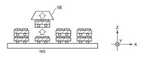
- FIG. 3 is a diagram for explaining the multi-stage temporary placement process in the first embodiment of the present invention.
- FIG. 4 is a diagram for explaining a connection process in the first embodiment of the present invention.
- FIG. 5 is a diagram for explaining a semiconductor device manufacturing apparatus according to the first embodiment of the present invention.
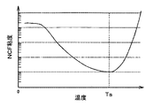
- FIG. 6 is a diagram for explaining the temperature-viscosity characteristics of the adhesive in the present invention.
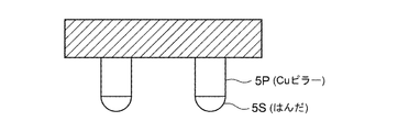
- FIG. 8 is a diagram illustrating the configuration of the pillar bump.
- a plurality of semiconductor chips 54 are arranged on a temporary substrate with the second main surface facing down.
- the temporary substrate only needs to have a surface state in which the semiconductor chip 54 is easily separated in a later process, and can be appropriately selected depending on the convenience of the process.
- a silicon substrate or a glass epoxy substrate may be used, a release material may be attached to a plate material or a stage, or a stage having an adsorption function may be used.
- the semiconductor chip 54 is a semiconductor chip made of a small piece of silicon, and bumps 55 made of solder at least at the tip are formed on the second main surface.
- solder made of Sn—Ag is used.
- the solder 5S is preferably formed at the tip of the copper pillar 5P, and its configuration is shown in FIG.
- a through electrode (not shown) is provided from the bump 55 on the second main surface of the semiconductor chip 54 to the first main surface on the opposite side, and an electrode pad 56 is provided on the first main surface side of the through electrode.
- the electrode pad 56 on the first main surface is electrically connected to the bump 55 on the second main surface via the through electrode. Further, the position of the electrode pad 56 and the position of the bump 55 differ only in the Z direction, and the position coordinates of X and Y are the same.
- the semiconductor device manufacturing apparatus 30 includes a control unit 20, an imaging device 11 including an X-ray sensor, an X-ray source 12, a monitor TV 14, a moving unit 15, a suction nozzle 16, and a pressure bonding head 13.
- the control unit 20 includes an inspection processing unit 21, a temporary arrangement processing unit 22, a multistage temporary arrangement processing unit 23, and a connection processing unit 24.
- the moving means 15 has a suction nozzle 16 and is configured to be able to move the suction nozzle 16 in the X, Y, and Z directions, and includes a heater inside to heat the suction nozzle 16.
- the crimping head 13 is also configured to be movable in the X, Y, and Z directions and can be heated by a heater.
- the captured fluoroscopic image is input to the inspection processing unit 21 in the control unit 20, and by performing image processing, the position of the electrode pad 56 of the semiconductor chip 54 and the position of the bump 5 of the semiconductor chip 4 (FIG. 1, FIG. 2), the positional deviation between the semiconductor chip 54 and the semiconductor chip 4 is recognized, and it is determined whether or not the positional deviation is within a predetermined range. Further, the fluoroscopic image captured by the imaging device 11 can be monitored by the monitor TV 14.
- the temporary arrangement processing unit 22 controls a temporary arrangement process described later. That is, the moving means 15 and the suction nozzle 16 are controlled to take out the semiconductor chip 4 from the container or the like and align the bumps 5 of the semiconductor chip 4 with the electrode pads 56 of the semiconductor chip 54 as shown in FIG. Temporary placement.
- the multi-stage temporary arrangement processing unit 23 controls a multi-stage temporary arrangement process to be described later, and among the temporary arrangement bodies 8 having the semiconductor chips 4 whose positional deviation is within a predetermined range, some temporary arrangement bodies 8 are absorbed by the suction nozzles 16. It is separated from the temporary substrate and stacked on another temporary arrangement body 8 having the semiconductor chip 8 in which the positional deviation remaining on the temporary substrate is within a predetermined range via the second adhesive 107.
- the arrangement body 108 is formed.
- connection processing unit 24 controls a connection process described later. That is, the crimping head 13 is driven and controlled to pressurize the temporary arrangement body 8 to electrically connect the bumps 5 of the semiconductor chip 4 and the electrode pads 56 of the semiconductor chip 54, as well as the first adhesive 7 and the first adhesive 7.
- the second adhesive 107 is heated to the curing temperature and cured.
- the semiconductor device manufacturing method according to the first embodiment is performed in the order of a temporary placement process, an inspection process, a multistage temporary placement process, and a connection process.
- the temporary placement process First, the temporary placement process will be described. As shown in FIG. 1, in the temporary placement step, the bumps 5 of the semiconductor chip 4 and the electrode pads 56 of the semiconductor chip 54 are positioned and temporarily placed via the first adhesive 7 so as to face each other.
- the semiconductor chip 4 has the same configuration as that of the semiconductor chip 54.
- a through electrode (not shown) is provided from the bump 5 on the second main surface to the first main surface on the opposite surface, and an electrode is formed on the first main surface side of the through electrode.
- a pad 6 is provided, whereby the electrode pad 6 on the first main surface is electrically connected to the bump 5 on the second main surface via the through electrode.
- the first adhesive 7 is a thermosetting non-conductive adhesive film (NCF), and is laminated in advance so as to enclose the bumps 5 on the second main surface of the semiconductor chip 4.
- NCF thermosetting non-conductive adhesive film
- the semiconductor chip 4 is temporarily placed on the semiconductor chip 54 by heating and pressurizing. Is done.
- the gap from the tip of the bump 5 of the semiconductor chip 4 to the surface of the electrode pad 56 of the semiconductor chip 54 is preferably 1 to 5 ⁇ m, more preferably 1 to 3 ⁇ m.
- This value is an experimentally obtained value. If the gap is made narrower or the bump 5 and the electrode pad 56 are brought into contact with each other, the bump 5-electrode pad is obtained when the two are connected in the connecting step described later. It has been found that the first adhesive 7 may remain between 56. Further, if the gap is made wider than this value, the semiconductor chip 4 may slip when the semiconductor chip 4 is pressurized in the connection process, which causes a serious displacement in quality.
- the viscosity of the first adhesive 7 varies depending on the temperature.
- the first adhesive 7 which is a thermosetting non-conductive adhesive film (NCF)
- NCF thermosetting non-conductive adhesive film
- the first adhesive 7 reversibly rises in temperature without being cured in a temperature range below the reference temperature Ts determined from its characteristics. Along with this, it exhibits the property of decreasing the viscosity, that is, the property of softening, and the property of increasing the viscosity when the temperature is lowered.
- NCF thermosetting non-conductive adhesive film
- the semiconductor chip 4 is temporarily placed by heating the first adhesive 7 to a temperature lower than the reference temperature Ts and softening. By leaving it after that, it is possible to prevent the temperature of the first adhesive 7 from being lowered and the viscosity to be increased and the semiconductor chip 4 from being displaced.
- a plurality of semiconductor chips 4 are temporarily placed on the semiconductor chip 54 via the first adhesive 7 to form a plurality of temporary placement bodies 8.
- the suction nozzle 16 is moved by the moving means 15 to suck the first main surface of the semiconductor chip 4 housed in a container or the like. Thereafter, the suction nozzle 16 is moved above the semiconductor chip 54 so that the electrode pad 56 of the semiconductor chip 54 and the bump 5 of the semiconductor chip 4 sucked by the suction nozzle 16 are opposed to each other, and then the suction nozzle 16 is moved to the semiconductor chip. It is heated and pressed close to the electrode pad 56 and temporarily disposed on the semiconductor chip 54.
- the gap between the bump 5 of the semiconductor chip 4 and the electrode pad 56 of the semiconductor chip 54 is kept within the above-described range. Further, when the positions of the electrode pads 56 of the semiconductor chip 54 before the semiconductor chip 4 is stacked are imaged in advance by an imaging device such as a CCD camera, and the positions are measured and stored, the stacking can be performed accurately.
- an inspection process is performed next.
- the inspection process will be described with reference to FIG.
- the positional deviation between the electrode pad 56 of the semiconductor chip 54 and the electrode pad 6 of the semiconductor chip 4 is inspected, and the temporary arrangement body 8 having the semiconductor chip 4 with the positional deviation within a predetermined range is used as the selected temporary arrangement body.
- the imaging device 11 captures X-rays from the X-ray source 12 to capture a perspective image of the bumps 5 of the semiconductor chip 4 and the electrode pads 56 of the semiconductor chip 54. The captured image is input to the inspection processing unit 21.
- the inspection processing unit 21 calculates the positional deviation of the semiconductor chip 4 in each temporary arrangement body 8 from the position of the electrode pad 56 of the semiconductor chip 54 and the position of the bump 5 of the semiconductor chip 4 from the captured image. Then, it is determined whether or not the calculated positional deviation is within a predetermined range, and the temporary arrangement body 8 having the semiconductor chip 4 within the predetermined range is specified as the selected temporary arrangement body.
- the imaging device 11 including the X-ray sensor and the X-ray source 12 are used to capture a perspective image of the electrode pad 56 of the semiconductor chip 54 and the bump 5 of the semiconductor chip 4.
- the imaging device 11 including the X-ray sensor and the X-ray source 12 are used to capture a perspective image of the electrode pad 56 of the semiconductor chip 54 and the bump 5 of the semiconductor chip 4.
- it is not necessarily limited to this, and can be appropriately selected depending on the convenience of the device configuration.
- an infrared sensor is provided as an imaging device, and infrared rays from an infrared source are transmitted through the temporary arrangement body 8 so that the electrode pads 56 of the semiconductor chip 54 and the bumps 5 of the semiconductor chip 4 are transmitted.
- the position of the electrode pad 56 of the semiconductor chip 54 before the semiconductor chip 4 is stacked may be measured and stored using a CCD camera, a CMOS sensor, or the like. After stacking the chips 4, the electrode pads 6 of the semiconductor chip 4 may be imaged with a CCD camera, a CMOS sensor, or the like, and the positional deviation between them may be inspected.
- the multi-stage temporary arrangement process will be described with reference to FIG.
- a part of the selected temporary arrangement bodies is adsorbed by the suction nozzle 16 and separated from the temporary substrate, and another selected temporary arrangement body remaining on the temporary substrate is used.
- the multi-stage temporary arrangement body 108 is formed by laminating via the second adhesive 107.
- the suction nozzle 16 sucks and holds the first main surface of the semiconductor chip 4 in a part of the selected temporary placement bodies to separate the selected temporary placement body from the temporary substrate, and another remaining on the temporary substrate.
- a multi-stage temporary arrangement body 108 is formed by laminating the first main surface of the semiconductor chip 4 of the selected temporary arrangement body via the second adhesive 107.
- the bump 55 of the lowermost semiconductor chip 54 of the selected temporary arrangement body adsorbed by the adsorption nozzle 16 and the electrode pad 6 of the uppermost semiconductor chip 4 of the selected temporary arrangement body remaining on the temporary substrate are arranged. Laminate so that they face each other.
- the second adhesive 107 remains on the second main surface of the semiconductor chip 54 or the temporary substrate of the selected temporary arrangement body in which the liquid thermosetting adhesive is adsorbed and separated by a coating nozzle (not shown).
- the selected temporary arrangement body is applied to the first main surface of the semiconductor chip 4.
- the second adhesive 107 is a liquid adhesive.
- the second adhesive 107 is not necessarily limited to this and can be appropriately selected.
- a thermosetting non-conductive adhesive film (NCF) similar to the first adhesive 7 may be used.
- the imaging device 11 captures X-rays from the X-ray source 12 so that the bumps 5 in the upper temporary selection body and the electrode pads in the lower temporary selection body are arranged.
- a fluoroscopic image with 56 is taken.
- the captured image is input to the inspection processing unit 21.
- the inspection processing unit 21 calculates a positional deviation in each selected temporary arrangement body from the bump 5 in the upper temporary selection arrangement body and the electrode pad 56 in the lower selection temporary arrangement body from the captured image. Then, it is determined whether or not the calculated positional deviation is within a predetermined range.
- connection process The connection process will be described with reference to FIG.
- the uppermost semiconductor chip 4 in the multi-stage temporary arrangement body 108 whose positional deviation on the temporary substrate is within a predetermined range is pressurized, and the bumps of each layer are brought into contact with the opposing electrode pads to be electrically connected.
- the first adhesive 7 and the second adhesive 107 are heated to the reference temperature Ts or higher to be cured.
- the pressure bonding head 13 is moved to above the multi-stage temporary arrangement bodies 108, and then the pressure bonding head 13 is brought close to the multi-stage temporary arrangement bodies 108, and the uppermost semiconductor chip 4 is heated and pressurized. Can do.
- a plurality of multi-stage temporary arrangement bodies 108 may be simultaneously heated and pressurized using a crimping head having an area including the plurality of multi-stage temporary arrangement bodies 108. .
- stacked the semiconductor chip 4 in multiple stages can be manufactured by repeating a temporary arrangement
- the multi-stage temporary arrangement step the multi-stage temporary arrangement body is sucked and held by the suction nozzle 16 and stacked on another temporary arrangement body.
- the semiconductor chip 4 whose positional deviation is not within a predetermined range may be sucked by the suction nozzle 16 and separated from the temporary placement body 8, and the temporary placement body 8 may be repaired.
- the first adhesive 7 can be easily separated by heating the first adhesive 7 to a temperature that is lower than the reference temperature Ts and softening it to reduce the viscosity.
- Example 1 a semiconductor device manufacturing method for manufacturing a semiconductor device by stacking semiconductor chips in multiple stages, Electrode pads are formed on the first main surface of each semiconductor chip, and bumps are formed on the second main surface.
- a positional deviation between a bump of a new semiconductor chip in the body and the electrode pad facing the bump, and a temporary arrangement body having a new semiconductor chip with the positional deviation within a predetermined range is selected as a temporary arrangement body
- the semiconductor chips are collectively heated and pressed to electrically connect the bumps and the electrode pads between the semiconductor chips and to cure the first adhesive and the second adhesive between the semiconductor chips.
- a semiconductor in which a plurality of semiconductor chips are stacked to electrically connect a bump formed on the second main surface of the upper semiconductor chip and an electrode pad formed on the first main surface of the lower semiconductor chip A device manufacturing device, An adsorption nozzle that adsorbs a semiconductor chip and temporarily arranges the semiconductor chip on a temporary substrate; and An imaging device that captures a fluoroscopic image through the semiconductor chips; and A pressure-bonding head that heats and pressurizes the semiconductor chips to electrically connect the electrode pads facing the bumps and cures the adhesive between the semiconductor chips; A controller that controls the suction nozzle, the imaging device, and the pressure-bonding head; The controller is A temporary placement processing unit that controls the suction nozzle to form a temporary placement body by facing the bumps and the electrode pads via a first adhesive; Based on the image picked up by the imaging device, the positional deviation between the semiconductor chips in the temporary arrangement body is inspected, and the temporary arrangement body having the semiconductor chips in which the positional deviation is in a predetermined range is specified as the
- An inspection processing unit to perform A multi-stage temporary arrangement processing unit which controls the suction nozzle to form a multi-stage temporary arrangement body by laminating a part of the selected temporary arrangement bodies on the temporary substrate on the temporary substrate via a second adhesive.
- the second embodiment of the present invention is different from the first embodiment in that a position correcting step of correcting the position by moving the semiconductor chip 4 whose positional deviation is not within a predetermined range is corrected.
- each process is performed in the order of a temporary placement process, an inspection process, a position correction process, a multistage temporary placement process, and a connection process.
- the temporary placement process, the inspection process, the multi-stage temporary placement process, and the connection process are the same as those in the first embodiment, and thus description thereof is omitted.
- the configuration of the semiconductor device manufacturing apparatus in the second embodiment is the same as that in the first embodiment, and thus the description thereof is omitted.
- the position correction process in the second embodiment will be described. If the semiconductor chip 4 whose positional deviation is not in the predetermined range, that is, the semiconductor chip 4 that is misaligned, is found in the inspection process in the first embodiment described above, the position correction is performed to eliminate the positional deviation of the semiconductor chip 4. Perform the process and correct its position. Then, the temporary arrangement body having the semiconductor chip 4 whose position is corrected is recognized as the selected temporary arrangement body. Specifically, it is carried out using the same suction nozzle 16 and moving means 15 as those used in the temporary placement step and the multistage temporary placement step described above.
- the semiconductor chip 104 is moved by heating the first adhesive 7 to a temperature that is lower than the reference temperature Ts and softens. Then, by leaving it after the position correction, it is possible to prevent the temperature of the first adhesive 7 from being lowered and the viscosity to be increased and the semiconductor chip 4 from being displaced.
- the position correction process is performed using the same suction nozzle 16 and moving means 15 as those used in the temporary placement process and the multi-stage temporary placement process.
- the position correction process is not necessarily limited to this. However, it can be changed as appropriate for the convenience of the device configuration. For example, a suction nozzle and moving means different from those used in the temporary placement step and the multistage temporary placement step may be provided separately.
- the selected temporary arrangement body which has been certified by correcting the position in the position correction process is also used as the multistage temporary arrangement body 108 for separation or lamination in the next multistage temporary arrangement process.
- the semiconductor chip 104 is moved by heating the second adhesive 107 to a temperature lower than the reference temperature Ts and softening.
- the bump in FIG. 7 is drawn round, it is preferable to use what has the solder 5S formed in the front-end
- the semiconductor chips can be connected to each other without any positional deviation, and the productivity in manufacturing the semiconductor device can be improved.
- the semiconductor device manufacturing method and the semiconductor device manufacturing apparatus according to the present invention can be widely used in the field of stacking semiconductor chips.
Landscapes
- Wire Bonding (AREA)
Abstract
半導体装置製造における生産性を向上させることを課題とする。具体的には、仮基板上に配置された半導体チップ54の第1主面に形成された電極パッド55に新たな半導体チップ4の第2主面に形成されたバンプ5を対向させ、第1の接着剤7を介して仮配置した仮配置体8を複数得た後、仮配置体8における半導体チップ4と、半導体チップ54との位置ズレを検査し、位置ズレが所定の範囲である仮配置体8を選択仮配置体として特定し、一部の選択仮配置体を仮基板より分離し仮基板上に残っている選択仮配置体に重ね、第2の接着剤107を介して仮配置した多段仮配置体108を得た後、多段仮配置体108における各半導体チップを一括して、加熱、加圧して半導体チップ間のバンプと電極パッドとを電気的に接続するとともに、半導体チップ間の第1及び第2の接着剤を硬化させる接続工程、とを備えた構成とした。
Description
本発明は、生産性を向上させた半導体装置の製造方法及び半導体装置の製造装置に関するものである。
近年、半導体チップを直接基板に実装する技術や半導体チップ同士を積層させて実装密度を高める技術の開発が進んでいる。
特許文献1には、複数の半導体チップを仮圧着して積層した後、一括して本圧着するようにして、半導体チップが高温に曝される回数を少なくした構成が記載されている。
特許文献1:特開2012-222038号公報
しかしながら、特許文献1記載のものは、仮圧着時に位置ズレの問題が発生していたとしてもそのまま本圧着工程に進むため、歩留まりが悪く生産性が低下するという問題があった。
本発明は、上記問題点を解決して、半導体装置製造における生産性を向上させることを課題とする。
上記課題を解決するために本発明は、半導体チップを多段に積層して半導体装置を製造する半導体装置の製造方法であって、
各半導体チップの第1主面には電極パッドが形成され第2主面にはバンプが形成されており、
(A)第1主面を上にして、複数の半導体チップを仮基板上に配置する配置工程、と
(B)新たな半導体チップの第2主面に形成されたバンプと、前記仮基板上に配置された半導体チップの第1主面に形成された電極パッドとを対向させ、第1の接着剤を介して仮配置した仮配置体を複数得る仮配置工程、と
(C)前記仮配置体における新たな半導体チップのバンプと、当該バンプと対向する前記電極パッドとの位置ズレを検査し、前記位置ズレが所定の範囲である新たな半導体チップを有する仮配置体を選択仮配置体として特定する検査工程、と
(D)一部の前記選択仮配置体を前記仮基板より分離し、この分離した選択仮配置体の最下層の半導体チップの第2主面に形成されたバンプと前記仮基板上の選択仮配置体における最上層の半導体チップの第1主面に形成された電極パッドとを対向させ、第2の接着剤を介して仮配置した多段仮配置体を得る多段仮配置工程、と
(E)前記多段仮配置体における各半導体チップを一括して、加熱、加圧して半導体チップ間のバンプと電極パッドとを電気的に接続するとともに、半導体チップ間の前記第1の接着剤及び前記第2の接着剤を硬化させる接続工程、と
を備えたことを特徴とする半導体装置の製造方法を提供するものである。
各半導体チップの第1主面には電極パッドが形成され第2主面にはバンプが形成されており、
(A)第1主面を上にして、複数の半導体チップを仮基板上に配置する配置工程、と
(B)新たな半導体チップの第2主面に形成されたバンプと、前記仮基板上に配置された半導体チップの第1主面に形成された電極パッドとを対向させ、第1の接着剤を介して仮配置した仮配置体を複数得る仮配置工程、と
(C)前記仮配置体における新たな半導体チップのバンプと、当該バンプと対向する前記電極パッドとの位置ズレを検査し、前記位置ズレが所定の範囲である新たな半導体チップを有する仮配置体を選択仮配置体として特定する検査工程、と
(D)一部の前記選択仮配置体を前記仮基板より分離し、この分離した選択仮配置体の最下層の半導体チップの第2主面に形成されたバンプと前記仮基板上の選択仮配置体における最上層の半導体チップの第1主面に形成された電極パッドとを対向させ、第2の接着剤を介して仮配置した多段仮配置体を得る多段仮配置工程、と
(E)前記多段仮配置体における各半導体チップを一括して、加熱、加圧して半導体チップ間のバンプと電極パッドとを電気的に接続するとともに、半導体チップ間の前記第1の接着剤及び前記第2の接着剤を硬化させる接続工程、と
を備えたことを特徴とする半導体装置の製造方法を提供するものである。
この構成により、位置ズレのない半導体チップを積層することができ、半導体装置製造における生産性を向上させることができる。
前記検査工程(C)と前記多段仮配置工程(D)との間に、(C1)前記位置ズレが所定の範囲にない新たな半導体チップがあれば、当該新たな半導体チップを移動させて位置修正し、当該仮配置体を選択仮配置体として認定する位置修正工程を備えるようにしてもよい。
この構成より、位置ズレをなくして半導体チップ同士を接続することができ、半導体装置製造における生産性を向上させることができる。
前記第1の接着剤は熱硬化性の非導電性接着フィルムであり、前記位置修正工程(C1)においては、前記第1の接着剤が軟化する温度に加熱して、前記位置ズレが所定の範囲にない新たな半導体チップを移動させるようにしてもよい。
この構成により、容易に半導体チップの位置を修正することができる。
また、上記課題を解決するために本発明は、複数の半導体チップを積層して、上層の半導体チップの第2主面に形成されたバンプと、下層の半導体チップの第1主面に形成された電極パッドとを電気的に接続する半導体装置の製造装置であって、半導体チップを吸着して仮基板上に配置された半導体チップに仮配置する吸着ノズルと、半導体チップ同士を透過させて透視画像を撮像する撮像装置と、前記半導体チップ同士を加熱、加圧して前記バンプと対向する前記電極パッドとを電気的に接続するとともに、半導体チップ間の接着剤を硬化させる圧着ヘッドと、前記吸着ノズル、前記撮像装置、及び前記圧着ヘッドを制御する制御部と、を備え、前記制御部は、前記吸着ノズルを制御して、第1の接着剤を介して前記バンプと前記電極パッドとを対向させて仮配置体を形成する仮配置処理部と、前記撮像装置が撮像した画像に基づいて、前記仮配置体における各半導体チップ間の位置ズレを検査し、前記位置ズレが所定の範囲にある半導体チップを有する仮配置体を選択仮配置体として特定する検査処理部と、前記吸着ノズルを制御して、一部の前記選択仮配置体を前記仮基板上の選択仮配置体に第2の接着剤を介して積層して多段仮配置体を形成する多段仮配置処理部と、前記圧着ヘッドを制御して、前記多段仮配置体における前記バンプと前記電極パッドとを電気的に接続するとともに前記第1の接着剤及び前記第2の接着剤を硬化させる接続処理部と、を有したことを特徴とする半導体装置の製造装置を提供するものである。
この構成により、位置ズレのない半導体チップを積層することができ、半導体装置製造における生産性を向上させることができる。
本発明の半導体装置の製造方法及び半導体装置の製造装置により、位置ズレのない半導体チップを積層することができ、半導体装置製造における生産性を向上させることができる。
本発明の実施例1について、図1~図6、図8を参照しながら説明する。図1は、本発明の実施例1における半導体チップの仮配置工程を説明する図である。図2は、本発明の実施例1における検査工程を説明する図である。図3は、本発明の実施例1における多段仮配置工程を説明する図である。図4は、本発明の実施例1における接続工程を説明する図である。図5は、本発明の実施例1における半導体装置の製造装置を説明する図である。図6は、本発明における接着剤の温度-粘度特性を説明する図である。図8は、ピラーバンプの構成を説明する図である。
(ベースとなる半導体チップの準備)
図1に示すように、複数の半導体チップ54をその第2主面を下にして、仮基板の上に配置しておく。仮基板は、後工程で半導体チップ54が分離しやすい表面状態のものであればよく、適宜、工程の都合により選択できる。例えば、シリコン基板やガラエポ基板を用いてもよいし、板材やステージに離型紙を貼りつけたものでもよいし、吸着機能のあるステージを用いてもよい。半導体チップ54は、小片のシリコンからなる半導体チップであり、その第2主面には少なくとも先端がはんだからなるバンプ55が形成されている。実施例1においては、Sn-Agからなるはんだが用いられている。なお、図1~図4におけるバンプ5は丸く描いているが、好ましくは、銅ピラー5Pの先端にはんだ5Sが形成されているものであり、その構成を図8に示す。半導体チップ54の第2主面におけるバンプ55から反対面の第1主面まで図示しない貫通電極が設けられ、この貫通電極の第1主面側には電極パッド56が設けられており、これによって、第1主面の電極パッド56は、貫通電極を介して第2主面のバンプ55に電気的に接続されている。また、電極パッド56の位置とバンプ55の位置とはZ方向に異なっているのみであって、X、Yの位置座標は同一である。
図1に示すように、複数の半導体チップ54をその第2主面を下にして、仮基板の上に配置しておく。仮基板は、後工程で半導体チップ54が分離しやすい表面状態のものであればよく、適宜、工程の都合により選択できる。例えば、シリコン基板やガラエポ基板を用いてもよいし、板材やステージに離型紙を貼りつけたものでもよいし、吸着機能のあるステージを用いてもよい。半導体チップ54は、小片のシリコンからなる半導体チップであり、その第2主面には少なくとも先端がはんだからなるバンプ55が形成されている。実施例1においては、Sn-Agからなるはんだが用いられている。なお、図1~図4におけるバンプ5は丸く描いているが、好ましくは、銅ピラー5Pの先端にはんだ5Sが形成されているものであり、その構成を図8に示す。半導体チップ54の第2主面におけるバンプ55から反対面の第1主面まで図示しない貫通電極が設けられ、この貫通電極の第1主面側には電極パッド56が設けられており、これによって、第1主面の電極パッド56は、貫通電極を介して第2主面のバンプ55に電気的に接続されている。また、電極パッド56の位置とバンプ55の位置とはZ方向に異なっているのみであって、X、Yの位置座標は同一である。
(半導体装置の製造装置)
本発明の実施例1における半導体装置の製造装置30について、図5を参照して説明する。半導体装置の製造装置30は、制御部20、X線センサからなる撮像装置11、X線源12、モニタTV14、移動手段15、吸着ノズル16、及び圧着ヘッド13を含んでいる。制御部20は、検査処理部21、仮配置処理部22、多段仮配置処理部23、及び接続処理部24を備えている。移動手段15は、吸着ノズル16を有して、この吸着ノズル16をX、Y、Z方向に移動可能に構成されるとともに、内部にヒータを含んでいて加熱することが可能となっている。また、圧着ヘッド13もX,Y、Z方向に移動可能に構成されているとともに、ヒータにより加熱することができる。
本発明の実施例1における半導体装置の製造装置30について、図5を参照して説明する。半導体装置の製造装置30は、制御部20、X線センサからなる撮像装置11、X線源12、モニタTV14、移動手段15、吸着ノズル16、及び圧着ヘッド13を含んでいる。制御部20は、検査処理部21、仮配置処理部22、多段仮配置処理部23、及び接続処理部24を備えている。移動手段15は、吸着ノズル16を有して、この吸着ノズル16をX、Y、Z方向に移動可能に構成されるとともに、内部にヒータを含んでいて加熱することが可能となっている。また、圧着ヘッド13もX,Y、Z方向に移動可能に構成されているとともに、ヒータにより加熱することができる。
X線源12で発生させたX線を積層された半導体チップに入射させ、透過したX線を撮像装置11で撮像して、バンプと電極パッドとの透視画像を得る。撮像された透視画像は、制御部20における検査処理部21に入力され、画像処理を実施することにより、半導体チップ54の電極パッド56の位置、及び半導体チップ4のバンプ5の位置(図1、図2参照)を計測し、半導体チップ54と半導体チップ4との位置ズレを認識して、この位置ズレが予め定めた所定の範囲であるか否かを判断する。また、撮像装置11が撮像した透視画像は、モニタTV14でモニタすることができる。
仮配置処理部22は、後述する仮配置工程を制御する。すなわち、移動手段15と吸着ノズル16を制御して、半導体チップ4を容器等から取り出し、半導体チップ54の電極パッド56に半導体チップ4のバンプ5を対向させるように位置合わせして図1のように仮配置する。
多段仮配置処理部23は、後述する多段仮配置工程を制御し、位置ズレが所定の範囲である半導体チップ4を有する仮配置体8のうち、一部の仮配置体8を吸着ノズル16で吸着して仮基板上から分離し、仮基板上に残っている位置ズレが所定の範囲である半導体チップ8を有する別の仮配置体8に第2の接着剤107を介して積層し多段仮配置体108を形成する。
接続処理部24は、後述する接続工程を制御する。すなわち、圧着ヘッド13を駆動制御して、仮配置体8を加圧して半導体チップ4のバンプ5と半導体チップ54の電極パッド56とを電気的に接続するとともに、第1の接着剤7及び第2の接着剤107を硬化温度に加熱して硬化させる。
実施例1における半導体装置の製造方法は、仮配置工程、検査工程、多段仮配置工程、接続工程の順に行われる。
(仮配置工程)
最初に、仮配置工程について説明する。図1に示すように仮配置工程では、第1の接着剤7を介して、半導体チップ4のバンプ5と半導体チップ54の電極パッド56とを対向させるように位置決めして仮配置する。半導体チップ4も半導体チップ54と同様の構成であり、第2主面のバンプ5から反対面の第1主面まで図示しない貫通電極が設けられ、この貫通電極の第1主面側には電極パッド6が設けられており、これによって、第1主面の電極パッド6は、貫通電極を介して第2主面のバンプ5に電気的に接続されている。また、電極パッド6の位置とバンプ5の位置とはZ方向に異なっているのみであって、X、Yの位置座標は同一である。第1の接着剤7は、熱硬化性の非導電性接着フィルム(NCF)であり、予め半導体チップ4の第2主面にバンプ5を内包するようにラミネートされている。仮配置工程では、半導体チップ4が加熱、加圧して半導体チップ54に仮配置されるが、半導体チップ54の電極パッド56に半導体チップ4のバンプ5が接触しないように間隙を有して仮配置される。半導体チップ4のバンプ5の先端から半導体チップ54の電極パッド56の表面までの間隙は1~5μmが好ましく、より好ましくは1~3μmである。
最初に、仮配置工程について説明する。図1に示すように仮配置工程では、第1の接着剤7を介して、半導体チップ4のバンプ5と半導体チップ54の電極パッド56とを対向させるように位置決めして仮配置する。半導体チップ4も半導体チップ54と同様の構成であり、第2主面のバンプ5から反対面の第1主面まで図示しない貫通電極が設けられ、この貫通電極の第1主面側には電極パッド6が設けられており、これによって、第1主面の電極パッド6は、貫通電極を介して第2主面のバンプ5に電気的に接続されている。また、電極パッド6の位置とバンプ5の位置とはZ方向に異なっているのみであって、X、Yの位置座標は同一である。第1の接着剤7は、熱硬化性の非導電性接着フィルム(NCF)であり、予め半導体チップ4の第2主面にバンプ5を内包するようにラミネートされている。仮配置工程では、半導体チップ4が加熱、加圧して半導体チップ54に仮配置されるが、半導体チップ54の電極パッド56に半導体チップ4のバンプ5が接触しないように間隙を有して仮配置される。半導体チップ4のバンプ5の先端から半導体チップ54の電極パッド56の表面までの間隙は1~5μmが好ましく、より好ましくは1~3μmである。
この値は、実験的に求めた値であり、これより間隙を狭くしたりバンプ5と電極パッド56とを接触させたりすると、後述する接続工程で両者を接続したときに、バンプ5-電極パッド56間に第1の接着剤7が残留する可能性があることがわかっている。また、この値より間隙を広くすると、接続工程で半導体チップ4を加圧したときに、半導体チップ4が滑って位置ズレが発生する可能性があり、品質に重大な問題となる。
第1の接着剤7は、図6に示すように、その温度に応じて粘度が変動する。具体的には、熱硬化性の非導電性接着フィルム(NCF)である第1の接着剤7は、その特性から定まる基準温度Ts未満の温度域においては硬化することなく、可逆的に温度上昇に伴って粘度が低くなる性質、つまり軟化する性質を示し、また、温度を低下させると粘度が高くなる性質を示す。一方、基準温度Ts以上の温度域においては硬化し、不可逆的に温度上昇に伴って粘度が高くなる性質を示す。つまり、基準温度Ts以上に一旦加熱すると温度が低下しても粘度が低下することはなく硬化状態となる。
そのため、仮配置工程においては、第1の接着剤7を基準温度Ts未満の温度であり軟化する温度に加熱して半導体チップ4を仮配置する。その後放置することにより、第1の接着剤7の温度が下がって粘度が高くなり半導体チップ4が位置ズレすることを防止できる。
仮配置工程では、複数の半導体チップ4を半導体チップ54上に第1の接着剤7を介して仮配置して複数の仮配置体8を形成する。具体的には、移動手段15により吸着ノズル16を移動させて容器等に収納されている半導体チップ4の第1主面を吸着する。その後、吸着ノズル16を半導体チップ54の上方に移動させ、半導体チップ54の電極パッド56と吸着ノズル16で吸着している半導体チップ4のバンプ5とを対向させた後、吸着ノズル16を半導体チップ54の電極パッド56に近づけて加熱、加圧して半導体チップ54上に仮配置する。ここで、前述したように、半導体チップ4のバンプ5と半導体チップ54の電極パッド56との間隙は前述した範囲内に止めておく。また、半導体チップ4を積層する前の半導体チップ54の電極パッド56の位置を予めCCDカメラ等の撮像装置で撮像して位置を計測して記憶しておくと正確に積層することができる。
(検査工程)
複数の仮配置体8を形成したら、次は、検査工程を実施する。図2を参照しながら、検査工程を説明する。検査工程では、半導体チップ54の電極パッド56と半導体チップ4の電極パッド6との位置ズレを検査し、位置ズレが所定の範囲にある半導体チップ4を有する仮配置体8を選択仮配置体として特定する。具体的には、撮像装置11がX線源12からのX線を撮像することにより、半導体チップ4のバンプ5と半導体チップ54の電極パッド56との透視画像を撮像する。撮像画像は、検査処理部21に入力される。検査処理部21は、撮像画像から半導体チップ54の電極パッド56の位置と、半導体チップ4のバンプ5の位置とから、各仮配置体8における半導体チップ4の位置ズレを算出する。そして算出した位置ズレが予め定めた所定の範囲であるか否かを判断し、所定の範囲にある半導体チップ4を有する仮配置体8を選択仮配置体として特定する。
複数の仮配置体8を形成したら、次は、検査工程を実施する。図2を参照しながら、検査工程を説明する。検査工程では、半導体チップ54の電極パッド56と半導体チップ4の電極パッド6との位置ズレを検査し、位置ズレが所定の範囲にある半導体チップ4を有する仮配置体8を選択仮配置体として特定する。具体的には、撮像装置11がX線源12からのX線を撮像することにより、半導体チップ4のバンプ5と半導体チップ54の電極パッド56との透視画像を撮像する。撮像画像は、検査処理部21に入力される。検査処理部21は、撮像画像から半導体チップ54の電極パッド56の位置と、半導体チップ4のバンプ5の位置とから、各仮配置体8における半導体チップ4の位置ズレを算出する。そして算出した位置ズレが予め定めた所定の範囲であるか否かを判断し、所定の範囲にある半導体チップ4を有する仮配置体8を選択仮配置体として特定する。
なお、実施例1においては、X線センサからなる撮像装置11とX線源12とを用いて、半導体チップ54の電極パッド56と半導体チップ4のバンプ5の透視画像を撮像するように構成したが、必ずしもこれに限定されず、装置構成の都合により適宜、選択することができる。例えば、仮基板にシリコン基板を用いた場合に撮像装置として赤外線センサを設けて、赤外線源からの赤外線を仮配置体8に透過させて、半導体チップ54の電極パッド56と半導体チップ4のバンプ5の透視画像を撮像するようにしてもよいし、CCDカメラやCMOSセンサ等を用いて、半導体チップ4を積層する前の半導体チップ54の電極パッド56の位置を計測、記憶しておいて、半導体チップ4を積層した後、当該半導体チップ4の電極パッド6をCCDカメラやCMOSセンサ等で撮像し、両者の位置ズレを検査するようにしてもよい。
(多段仮配置工程)
図3を参照しながら、多段仮配置工程を説明する。前述した検査工程で特定した選択仮配置体のうち、一部の選択仮配置体を吸着ノズル16で吸着して仮基板上から分離し、仮基板上に残っている別の選択仮置体に第2の接着剤107を介して積層し多段仮配置体108を形成する。具体的には、吸着ノズル16で一部の選択仮配置体における半導体チップ4の第1主面を吸着保持して選択仮配置体を仮基板から分離し、仮基板上に残っている別の選択仮配置体の半導体チップ4の第1主面に第2の接着剤107を介して積層して多段仮配置体108を形成する。その際、吸着ノズル16で吸着している選択仮配置体の最下層の半導体チップ54のバンプ55と仮基板上に残っている選択仮配置体の最上層の半導体チップ4の電極パッド6とを対向させるように積層する。第2の接着剤107は、積層の前に、図示しない塗布ノズルで液状の熱硬化性接着剤を吸着・分離した選択仮配置体の半導体チップ54の第2主面、又は仮基板上に残っている選択仮配置体の半導体チップ4の第1主面に塗布する。
図3を参照しながら、多段仮配置工程を説明する。前述した検査工程で特定した選択仮配置体のうち、一部の選択仮配置体を吸着ノズル16で吸着して仮基板上から分離し、仮基板上に残っている別の選択仮置体に第2の接着剤107を介して積層し多段仮配置体108を形成する。具体的には、吸着ノズル16で一部の選択仮配置体における半導体チップ4の第1主面を吸着保持して選択仮配置体を仮基板から分離し、仮基板上に残っている別の選択仮配置体の半導体チップ4の第1主面に第2の接着剤107を介して積層して多段仮配置体108を形成する。その際、吸着ノズル16で吸着している選択仮配置体の最下層の半導体チップ54のバンプ55と仮基板上に残っている選択仮配置体の最上層の半導体チップ4の電極パッド6とを対向させるように積層する。第2の接着剤107は、積層の前に、図示しない塗布ノズルで液状の熱硬化性接着剤を吸着・分離した選択仮配置体の半導体チップ54の第2主面、又は仮基板上に残っている選択仮配置体の半導体チップ4の第1主面に塗布する。
なお、実施例1においては、第2の接着剤107を液状の接着剤としたが、必ずしもこれに限定されず、適宜、選択することができる。例えば、第1の接着剤7と同様の熱硬化性の非導電性接着フィルム(NCF)としてもよい。
なお、多段仮配置体108を形成した後、各選択仮配置体同士の位置ズレを検査するようにしてもよい。これにより、選択仮配置体同士の位置ズレを防いで多段仮配置体108を形成することができる。具体的には、前述した検査工程と同様に、撮像装置11がX線源12からのX線を撮像することにより、上層の選択仮配置体におけるバンプ5と下層の選択仮配置体における電極パッド56との透視画像を撮像する。撮像画像は、検査処理部21に入力される。検査処理部21は、撮像画像から上層の選択仮配置体におけるバンプ5と下層の選択仮配置体における電極パッド56とから、各選択仮配置体における位置ズレを算出する。そして算出した位置ズレが予め定めた所定の範囲であるか否かを判断する。
(接続工程)
図4を参照しながら、接続工程を説明する。接続工程では、仮基板上の位置ズレが所定の範囲である多段仮配置体108における最上層の半導体チップ4を加圧して、各層のバンプを対向する電極パッドに接触させて電気的に接続するとともに、第1の接着剤7及び第2の接着剤107を基準温度Ts以上に加熱して硬化させる。具体的には、圧着ヘッド13を各多段仮配置体108の上方まで移動させ、次に圧着ヘッド13を多段仮配置体108に近づけ、最上層の半導体チップ4を加熱、加圧することにより行うことができる。
図4を参照しながら、接続工程を説明する。接続工程では、仮基板上の位置ズレが所定の範囲である多段仮配置体108における最上層の半導体チップ4を加圧して、各層のバンプを対向する電極パッドに接触させて電気的に接続するとともに、第1の接着剤7及び第2の接着剤107を基準温度Ts以上に加熱して硬化させる。具体的には、圧着ヘッド13を各多段仮配置体108の上方まで移動させ、次に圧着ヘッド13を多段仮配置体108に近づけ、最上層の半導体チップ4を加熱、加圧することにより行うことができる。
この接続工程は、10秒程度の時間を要するので、複数の多段仮配置体108を含む面積を有する圧着ヘッドを用いて、複数の多段仮配置体108を同時に加熱、加圧するようにしてもよい。
なお、仮配置工程、及び検査工程を繰り返すことにより、半導体チップ4を多段に積層した仮配置体を製造することができる。この場合、多段仮配置工程では、吸着ノズル16で多段の仮配置体を吸着保持し、別の仮配置体に積層させる。
なお、検査工程の後に、位置ズレが所定の範囲にない半導体チップ4を吸着ノズル16で吸着して仮配置体8から分離し、この仮配置体8をリペアするように構成してもよい。半導体チップ4を仮配置体8から分離する場合は、第1の接着剤7を基準温度Ts未満の温度であり軟化する温度に加熱して粘度を低下させると容易に分離できる。
このように、実施例1においては、半導体チップを多段に積層して半導体装置を製造する半導体装置の製造方法であって、
各半導体チップの第1主面には電極パッドが形成され第2主面にはバンプが形成されており、
(A)第1主面を上にして、複数の半導体チップを仮基板上に配置する配置工程、と
(B)新たな半導体チップの第2主面に形成されたバンプと、前記仮基板上に配置された半導体チップの第1主面に形成された電極パッドとを対向させ、第1の接着剤を介して仮配置した仮配置体を複数得る仮配置工程、と
(C)前記仮配置体における新たな半導体チップのバンプと、当該バンプと対向する前記電極パッドとの位置ズレを検査し、前記位置ズレが所定の範囲である新たな半導体チップを有する仮配置体を選択仮配置体として特定する検査工程、と
(D)一部の前記選択仮配置体を前記仮基板より分離し、この分離した選択仮配置体の最下層の半導体チップの第2主面に形成されたバンプと前記仮基板上の選択仮配置体における最上層の半導体チップの第1主面に形成された電極パッドとを対向させ、第2の接着剤を介して仮配置した多段仮配置体を得る多段仮配置工程、と
(E)前記多段仮配置体における各半導体チップを一括して、加熱、加圧して半導体チップ間のバンプと電極パッドとを電気的に接続するとともに、半導体チップ間の前記第1の接着剤及び前記第2の接着剤を硬化させる接続工程、と
を備えたことを特徴とする半導体装置の製造方法により、位置ズレのない半導体チップを積層することができ、半導体装置製造における生産性を向上させることができる。
各半導体チップの第1主面には電極パッドが形成され第2主面にはバンプが形成されており、
(A)第1主面を上にして、複数の半導体チップを仮基板上に配置する配置工程、と
(B)新たな半導体チップの第2主面に形成されたバンプと、前記仮基板上に配置された半導体チップの第1主面に形成された電極パッドとを対向させ、第1の接着剤を介して仮配置した仮配置体を複数得る仮配置工程、と
(C)前記仮配置体における新たな半導体チップのバンプと、当該バンプと対向する前記電極パッドとの位置ズレを検査し、前記位置ズレが所定の範囲である新たな半導体チップを有する仮配置体を選択仮配置体として特定する検査工程、と
(D)一部の前記選択仮配置体を前記仮基板より分離し、この分離した選択仮配置体の最下層の半導体チップの第2主面に形成されたバンプと前記仮基板上の選択仮配置体における最上層の半導体チップの第1主面に形成された電極パッドとを対向させ、第2の接着剤を介して仮配置した多段仮配置体を得る多段仮配置工程、と
(E)前記多段仮配置体における各半導体チップを一括して、加熱、加圧して半導体チップ間のバンプと電極パッドとを電気的に接続するとともに、半導体チップ間の前記第1の接着剤及び前記第2の接着剤を硬化させる接続工程、と
を備えたことを特徴とする半導体装置の製造方法により、位置ズレのない半導体チップを積層することができ、半導体装置製造における生産性を向上させることができる。
また、複数の半導体チップを積層して、上層の半導体チップの第2主面に形成されたバンプと、下層の半導体チップの第1主面に形成された電極パッドとを電気的に接続する半導体装置の製造装置であって、
半導体チップを吸着して仮基板上に配置された半導体チップに仮配置する吸着ノズルと、
半導体チップ同士を透過させて透視画像を撮像する撮像装置と、
前記半導体チップ同士を加熱、加圧して前記バンプと対向する前記電極パッドとを電気的に接続するとともに、半導体チップ間の接着剤を硬化させる圧着ヘッドと、
前記吸着ノズル、前記撮像装置、及び前記圧着ヘッドを制御する制御部と、を備え、
前記制御部は、
前記吸着ノズルを制御して、第1の接着剤を介して前記バンプと前記電極パッドとを対向させて仮配置体を形成する仮配置処理部と、
前記撮像装置が撮像した画像に基づいて、前記仮配置体における各半導体チップ間の位置ズレを検査し、前記位置ズレが所定の範囲にある半導体チップを有する仮配置体を選択仮配置体として特定する検査処理部と、
前記吸着ノズルを制御して、一部の前記選択仮配置体を前記仮基板上の選択仮配置体に第2の接着剤を介して積層して多段仮配置体を形成する多段仮配置処理部と、
前記圧着ヘッドを制御して、前記多段仮配置体における前記バンプと前記電極パッドとを電気的に接続するとともに前記第1の接着剤及び前記第2の接着剤を硬化させる接続処理部と、を有したことを特徴とする半導体装置の製造装置により、位置ズレのない半導体チップを積層することができ、半導体装置製造における生産性を向上させることができる。
半導体チップを吸着して仮基板上に配置された半導体チップに仮配置する吸着ノズルと、
半導体チップ同士を透過させて透視画像を撮像する撮像装置と、
前記半導体チップ同士を加熱、加圧して前記バンプと対向する前記電極パッドとを電気的に接続するとともに、半導体チップ間の接着剤を硬化させる圧着ヘッドと、
前記吸着ノズル、前記撮像装置、及び前記圧着ヘッドを制御する制御部と、を備え、
前記制御部は、
前記吸着ノズルを制御して、第1の接着剤を介して前記バンプと前記電極パッドとを対向させて仮配置体を形成する仮配置処理部と、
前記撮像装置が撮像した画像に基づいて、前記仮配置体における各半導体チップ間の位置ズレを検査し、前記位置ズレが所定の範囲にある半導体チップを有する仮配置体を選択仮配置体として特定する検査処理部と、
前記吸着ノズルを制御して、一部の前記選択仮配置体を前記仮基板上の選択仮配置体に第2の接着剤を介して積層して多段仮配置体を形成する多段仮配置処理部と、
前記圧着ヘッドを制御して、前記多段仮配置体における前記バンプと前記電極パッドとを電気的に接続するとともに前記第1の接着剤及び前記第2の接着剤を硬化させる接続処理部と、を有したことを特徴とする半導体装置の製造装置により、位置ズレのない半導体チップを積層することができ、半導体装置製造における生産性を向上させることができる。
本発明の実施例2は、位置ズレが所定の範囲にない半導体チップ4の位置ズレを解消すべく移動させて位置修正する位置修正工程を加えた点で実施例1に対して異なっている。
実施例2における半導体装置の製造方法は、仮配置工程、検査工程、位置修正工程、多段仮配置工程、接続工程の順に各工程を実施する。このうち、仮配置工程、検査工程、多段仮配置工程、及び接続工程は、実施例1と同じであるので、説明を省略する。また、実施例2における半導体装置の製造装置の構成は、実施例1と同じであるので、説明を省略する。
(位置修正工程)
図7を参照しながら、実施例2における位置修正工程を説明する。前述した実施例1における検査工程で、位置ズレが所定の範囲にない半導体チップ4、すなわち、位置ズレした半導体チップ4が発見されれば、当該半導体チップ4の位置ズレを解消すべく、位置修正工程を実施してその位置を修正する。そして、位置修正した半導体チップ4を有する仮配置体を選択仮配置体として認定する。具体的には、前述した仮配置工程や多段仮配置工程で使用したものと同じ吸着ノズル16と移動手段15とを用いて実施する。つまり、吸着ノズル16で位置ズレした半導体チップ4の第1主面を吸着保持したまま、位置ズレの逆向きに移動手段15により、X、Y方向へ移動させる。この位置修正工程では、第1の接着剤7を基準温度Ts未満の温度であり軟化する温度に加熱して半導体チップ104を移動させる。そして、位置修正後、放置することにより、第1の接着剤7の温度が下がって粘度が高くなり半導体チップ4が位置ズレすることを防止できる。
図7を参照しながら、実施例2における位置修正工程を説明する。前述した実施例1における検査工程で、位置ズレが所定の範囲にない半導体チップ4、すなわち、位置ズレした半導体チップ4が発見されれば、当該半導体チップ4の位置ズレを解消すべく、位置修正工程を実施してその位置を修正する。そして、位置修正した半導体チップ4を有する仮配置体を選択仮配置体として認定する。具体的には、前述した仮配置工程や多段仮配置工程で使用したものと同じ吸着ノズル16と移動手段15とを用いて実施する。つまり、吸着ノズル16で位置ズレした半導体チップ4の第1主面を吸着保持したまま、位置ズレの逆向きに移動手段15により、X、Y方向へ移動させる。この位置修正工程では、第1の接着剤7を基準温度Ts未満の温度であり軟化する温度に加熱して半導体チップ104を移動させる。そして、位置修正後、放置することにより、第1の接着剤7の温度が下がって粘度が高くなり半導体チップ4が位置ズレすることを防止できる。
なお、実施例2においては、位置修正工程を、仮配置工程や多段仮配置工程で使用したものと同じ吸着ノズル16と移動手段15とを用いて実施するようにしたが、必ずしもこれに限定されず、装置構成の都合により適宜変更できる。例えば、仮配置工程や多段仮配置工程で使用したものとは異なる吸着ノズルや移動手段を別に設けて実施するようにしてもよい。
位置修正工程で位置修正して認定された選択仮配置体も、次の多段仮配置工程での分離又は積層に用いられて多段仮配置体108とされる。このとき、積層された多段仮配置体における選択仮配置体の位置ズレがないか検査をしてもよい。仮に位置ズレがあれば、前述の位置修正工程と同様に、この位置ズレを解消すべくX、Y方向に上層の選択仮配置体を移動させてもよい。これにより、位置ズレのない多段仮配置体108を形成できる。この場合、第2の接着剤107を基準温度Ts未満の温度であり軟化する温度に加熱して半導体チップ104を移動させる。
なお、図7におけるバンプは丸く描いているが、バンプとして銅ピラー5Pの先端にはんだ5Sが形成されているものを用いることが好ましい(図8参照)。
このように、実施例2においては、位置修正工程を実施することにより、位置ズレをなくして半導体チップ同士を接続することができ、半導体装置製造における生産性を向上させることができる。
本発明における半導体装置の製造方法及び半導体装置の製造装置は、半導体チップを積層する分野に広く用いることができる。
4:半導体チップ 5:バンプ 6:電極パッド 7:接着剤 8:仮配置体11:撮像装置 13:圧着ヘッド 14:モニタTV 15:移動手段 16:吸着ノズル20:制御部 21:検査処理部 22:仮配置処理部 23:多段仮配置処理部24:接続処理部 30:半導体装置の製造装置54:半導体チップ 55:バンプ 56:電極パッド 107:接着剤 108:多段仮配置体
Claims (4)
- 半導体チップを多段に積層して半導体装置を製造する半導体装置の製造方法であって、
各半導体チップの第1主面には電極パッドが形成され第2主面にはバンプが形成されており、
(A)第1主面を上にして、複数の半導体チップを仮基板上に配置する配置工程、と
(B)新たな半導体チップの第2主面に形成されたバンプと、前記仮基板上に配置された半導体チップの第1主面に形成された電極パッドとを対向させ、第1の接着剤を介して仮配置した仮配置体を複数得る仮配置工程、と
(C)前記仮配置体における新たな半導体チップのバンプと、当該バンプと対向する前記電極パッドとの位置ズレを検査し、前記位置ズレが所定の範囲である新たな半導体チップを有する仮配置体を選択仮配置体として特定する検査工程、と
(D)一部の前記選択仮配置体を前記仮基板より分離し、この分離した選択仮配置体の最下層の半導体チップの第2主面に形成されたバンプと前記仮基板上の選択仮配置体における最上層の半導体チップの第1主面に形成された電極パッドとを対向させ、第2の接着剤を介して仮配置した多段仮配置体を得る多段仮配置工程、と
(E)前記多段仮配置体における各半導体チップを一括して、加熱、加圧して半導体チップ間のバンプと電極パッドとを電気的に接続するとともに、半導体チップ間の前記第1の接着剤及び前記第2の接着剤を硬化させる接続工程、と
を備えたことを特徴とする半導体装置の製造方法。 - 前記検査工程(C)と前記多段仮配置工程(D)との間に、
(C1)前記位置ズレが所定の範囲にない新たな半導体チップがあれば、当該新たな半導体チップを移動させて位置修正し、当該仮配置体を選択仮配置体として認定する位置修正工程を備えたことを特徴とする請求項1に記載の半導体装置の製造方法。 - 前記第1の接着剤は熱硬化性の非導電性接着フィルムであり、前記位置修正工程(C1)においては、前記第1の接着剤が軟化する温度に加熱して、前記位置ズレが所定の範囲にない新たな半導体チップを移動させることを特徴とする請求項2に記載の半導体装置の製造方法。
- 複数の半導体チップを積層して、上層の半導体チップの第2主面に形成されたバンプと、下層の半導体チップの第1主面に形成された電極パッドとを電気的に接続する半導体装置の製造装置であって、
半導体チップを吸着して仮基板上に配置された半導体チップに仮配置する吸着ノズルと、半導体チップ同士を透過させて透視画像を撮像する撮像装置と、
前記半導体チップ同士を加熱、加圧して前記バンプと対向する前記電極パッドとを電気的に接続するとともに、半導体チップ間の接着剤を硬化させる圧着ヘッドと、
前記吸着ノズル、前記撮像装置、及び前記圧着ヘッドを制御する制御部と、を備え、
前記制御部は、
前記吸着ノズルを制御して、第1の接着剤を介して前記バンプと前記電極パッドとを対向させて仮配置体を形成する仮配置処理部と、
前記撮像装置が撮像した画像に基づいて、前記仮配置体における各半導体チップ間の位置ズレを検査し、前記位置ズレが所定の範囲にある半導体チップを有する仮配置体を選択仮配置体として特定する検査処理部と、
前記吸着ノズルを制御して、一部の前記選択仮配置体を前記仮基板上の選択仮配置体に第2の接着剤を介して積層して多段仮配置体を形成する多段仮配置処理部と、
前記圧着ヘッドを制御して、前記多段仮配置体における前記バンプと前記電極パッドとを電気的に接続するとともに前記第1の接着剤及び前記第2の接着剤を硬化させる接続処理部と、を有したことを特徴とする半導体装置の製造装置。
Priority Applications (2)
| Application Number | Priority Date | Filing Date | Title |
|---|---|---|---|
| KR1020187027597A KR102196325B1 (ko) | 2016-03-30 | 2017-03-21 | 반도체 장치의 제조 방법 및 반도체 장치의 제조 장치 |
| CN201780032694.9A CN109155304B (zh) | 2016-03-30 | 2017-03-21 | 半导体装置的制造方法和半导体装置的制造装置 |
Applications Claiming Priority (2)
| Application Number | Priority Date | Filing Date | Title |
|---|---|---|---|
| JP2016-067398 | 2016-03-30 | ||
| JP2016067398A JP6688543B2 (ja) | 2016-03-30 | 2016-03-30 | 半導体装置の製造方法及び半導体装置の製造装置 |
Publications (1)
| Publication Number | Publication Date |
|---|---|
| WO2017169944A1 true WO2017169944A1 (ja) | 2017-10-05 |
Family
ID=59964958
Family Applications (1)
| Application Number | Title | Priority Date | Filing Date |
|---|---|---|---|
| PCT/JP2017/011088 Ceased WO2017169944A1 (ja) | 2016-03-30 | 2017-03-21 | 半導体装置の製造方法及び半導体装置の製造装置 |
Country Status (4)
| Country | Link |
|---|---|
| JP (1) | JP6688543B2 (ja) |
| KR (1) | KR102196325B1 (ja) |
| CN (1) | CN109155304B (ja) |
| WO (1) | WO2017169944A1 (ja) |
Families Citing this family (2)
| Publication number | Priority date | Publication date | Assignee | Title |
|---|---|---|---|---|
| JP6349539B2 (ja) | 2016-09-30 | 2018-07-04 | 株式会社新川 | 半導体装置の製造方法および実装装置 |
| CN113013307A (zh) * | 2021-03-01 | 2021-06-22 | 东莞市中麒光电技术有限公司 | 一种显示模块故障芯片修复方法 |
Citations (6)
| Publication number | Priority date | Publication date | Assignee | Title |
|---|---|---|---|---|
| JP2002100728A (ja) * | 2000-09-25 | 2002-04-05 | Taiyo Yuden Co Ltd | チップ部品組立体の製造方法 |
| JP2006261264A (ja) * | 2005-03-16 | 2006-09-28 | Oki Electric Ind Co Ltd | チップの積層方法及びその方法を使用した半導体装置の製造方法 |
| JP2012222038A (ja) * | 2011-04-05 | 2012-11-12 | Elpida Memory Inc | 半導体装置の製造方法 |
| JP2013225642A (ja) * | 2011-11-11 | 2013-10-31 | Sumitomo Bakelite Co Ltd | 半導体装置の製造方法 |
| JP2015095499A (ja) * | 2013-11-11 | 2015-05-18 | 東レ株式会社 | 半導体装置の製造方法 |
| WO2015079991A1 (ja) * | 2013-11-27 | 2015-06-04 | 東レエンジニアリング株式会社 | 3次元実装方法および3次元実装装置 |
Family Cites Families (6)
| Publication number | Priority date | Publication date | Assignee | Title |
|---|---|---|---|---|
| JP3718205B2 (ja) * | 2003-07-04 | 2005-11-24 | 松下電器産業株式会社 | チップ積層型半導体装置およびその製造方法 |
| JP2007036143A (ja) * | 2005-07-29 | 2007-02-08 | Disco Abrasive Syst Ltd | 半導体ウエーハの加工方法 |
| JP2008177215A (ja) * | 2007-01-16 | 2008-07-31 | Sharp Corp | 基板貼り合わせ方法および基板貼り合わせ装置 |
| US20120287263A1 (en) * | 2009-11-16 | 2012-11-15 | Rudolph Technologies, Inc. | Infrared inspection of bonded substrates |
| JP5289484B2 (ja) * | 2011-03-04 | 2013-09-11 | 株式会社東芝 | 積層型半導体装置の製造方法 |
| US20150050778A1 (en) * | 2012-03-07 | 2015-02-19 | Toray Industries, Inc. | Method and apparatus for producing semiconductor device |
-
2016
- 2016-03-30 JP JP2016067398A patent/JP6688543B2/ja active Active
-
2017
- 2017-03-21 CN CN201780032694.9A patent/CN109155304B/zh active Active
- 2017-03-21 KR KR1020187027597A patent/KR102196325B1/ko active Active
- 2017-03-21 WO PCT/JP2017/011088 patent/WO2017169944A1/ja not_active Ceased
Patent Citations (6)
| Publication number | Priority date | Publication date | Assignee | Title |
|---|---|---|---|---|
| JP2002100728A (ja) * | 2000-09-25 | 2002-04-05 | Taiyo Yuden Co Ltd | チップ部品組立体の製造方法 |
| JP2006261264A (ja) * | 2005-03-16 | 2006-09-28 | Oki Electric Ind Co Ltd | チップの積層方法及びその方法を使用した半導体装置の製造方法 |
| JP2012222038A (ja) * | 2011-04-05 | 2012-11-12 | Elpida Memory Inc | 半導体装置の製造方法 |
| JP2013225642A (ja) * | 2011-11-11 | 2013-10-31 | Sumitomo Bakelite Co Ltd | 半導体装置の製造方法 |
| JP2015095499A (ja) * | 2013-11-11 | 2015-05-18 | 東レ株式会社 | 半導体装置の製造方法 |
| WO2015079991A1 (ja) * | 2013-11-27 | 2015-06-04 | 東レエンジニアリング株式会社 | 3次元実装方法および3次元実装装置 |
Also Published As
| Publication number | Publication date |
|---|---|
| JP2017183457A (ja) | 2017-10-05 |
| KR102196325B1 (ko) | 2020-12-29 |
| KR20180128412A (ko) | 2018-12-03 |
| JP6688543B2 (ja) | 2020-04-28 |
| CN109155304B (zh) | 2021-10-22 |
| CN109155304A (zh) | 2019-01-04 |
Similar Documents
| Publication | Publication Date | Title |
|---|---|---|
| KR102227444B1 (ko) | 반도체 장치의 제조 방법 및 제조 장치 | |
| KR102230921B1 (ko) | 반도체 장치의 제조 방법, 및 실장 장치 | |
| CN103377958B (zh) | 半导体芯片的热压缩键合 | |
| CN109103117B (zh) | 结合半导体芯片的设备和结合半导体芯片的方法 | |
| JP6349540B2 (ja) | 半導体チップの実装装置、および、半導体装置の製造方法 | |
| KR102147683B1 (ko) | 반도체 장치의 제조 방법 및 실장 장치 | |
| TWI746888B (zh) | 封裝裝置 | |
| WO2010016570A1 (ja) | ボンディング装置、ボンディング装置の補正量算出方法及びボンディング方法 | |
| WO2017169944A1 (ja) | 半導体装置の製造方法及び半導体装置の製造装置 | |
| JP6789791B2 (ja) | 半導体装置の製造装置および製造方法 | |
| JP6179843B2 (ja) | 実装装置及び実装方法 | |
| JP2016058542A (ja) | チップと基板との接合方法、チップと基板との仮接合装置、チップ実装システム | |
| JP6536024B2 (ja) | 半導体デバイスの製造方法及び半導体デバイス | |
| JP7317354B2 (ja) | 実装装置 | |
| WO2015105149A1 (ja) | 半導体装置の実装方法および実装装置 |
Legal Events
| Date | Code | Title | Description |
|---|---|---|---|
| ENP | Entry into the national phase |
Ref document number: 20187027597 Country of ref document: KR Kind code of ref document: A |
|
| NENP | Non-entry into the national phase |
Ref country code: DE |
|
| 121 | Ep: the epo has been informed by wipo that ep was designated in this application |
Ref document number: 17774485 Country of ref document: EP Kind code of ref document: A1 |
|
| 122 | Ep: pct application non-entry in european phase |
Ref document number: 17774485 Country of ref document: EP Kind code of ref document: A1 |