WO2017169686A1 - 電圧変換装置及び電圧変換方法 - Google Patents
電圧変換装置及び電圧変換方法 Download PDFInfo
- Publication number
- WO2017169686A1 WO2017169686A1 PCT/JP2017/009928 JP2017009928W WO2017169686A1 WO 2017169686 A1 WO2017169686 A1 WO 2017169686A1 JP 2017009928 W JP2017009928 W JP 2017009928W WO 2017169686 A1 WO2017169686 A1 WO 2017169686A1
- Authority
- WO
- WIPO (PCT)
- Prior art keywords
- switching
- pwm signal
- time
- frequency
- switching frequency
- Prior art date
- Legal status (The legal status is an assumption and is not a legal conclusion. Google has not performed a legal analysis and makes no representation as to the accuracy of the status listed.)
- Ceased
Links
Images


Classifications
-
- H—ELECTRICITY
- H03—ELECTRONIC CIRCUITRY
- H03K—PULSE TECHNIQUE
- H03K3/00—Circuits for generating electric pulses; Monostable, bistable or multistable circuits
- H03K3/01—Details
- H03K3/017—Adjustment of width or dutycycle of pulses
-
- H—ELECTRICITY
- H03—ELECTRONIC CIRCUITRY
- H03K—PULSE TECHNIQUE
- H03K7/00—Modulating pulses with a continuously-variable modulating signal
- H03K7/08—Duration or width modulation ; Duty cycle modulation
-
- H—ELECTRICITY
- H02—GENERATION; CONVERSION OR DISTRIBUTION OF ELECTRIC POWER
- H02M—APPARATUS FOR CONVERSION BETWEEN AC AND AC, BETWEEN AC AND DC, OR BETWEEN DC AND DC, AND FOR USE WITH MAINS OR SIMILAR POWER SUPPLY SYSTEMS; CONVERSION OF DC OR AC INPUT POWER INTO SURGE OUTPUT POWER; CONTROL OR REGULATION THEREOF
- H02M3/00—Conversion of DC power input into DC power output
- H02M3/02—Conversion of DC power input into DC power output without intermediate conversion into AC
- H02M3/04—Conversion of DC power input into DC power output without intermediate conversion into AC by static converters
- H02M3/10—Conversion of DC power input into DC power output without intermediate conversion into AC by static converters using discharge tubes with control electrode or semiconductor devices with control electrode
- H02M3/145—Conversion of DC power input into DC power output without intermediate conversion into AC by static converters using discharge tubes with control electrode or semiconductor devices with control electrode using devices of a triode or transistor type requiring continuous application of a control signal
- H02M3/155—Conversion of DC power input into DC power output without intermediate conversion into AC by static converters using discharge tubes with control electrode or semiconductor devices with control electrode using devices of a triode or transistor type requiring continuous application of a control signal using semiconductor devices only
-
- H—ELECTRICITY
- H03—ELECTRONIC CIRCUITRY
- H03K—PULSE TECHNIQUE
- H03K17/00—Electronic switching or gating, i.e. not by contact-making and –breaking
- H03K17/51—Electronic switching or gating, i.e. not by contact-making and –breaking characterised by the components used
- H03K17/56—Electronic switching or gating, i.e. not by contact-making and –breaking characterised by the components used by the use, as active elements, of semiconductor devices
- H03K17/60—Electronic switching or gating, i.e. not by contact-making and –breaking characterised by the components used by the use, as active elements, of semiconductor devices the devices being bipolar transistors
- H03K17/64—Electronic switching or gating, i.e. not by contact-making and –breaking characterised by the components used by the use, as active elements, of semiconductor devices the devices being bipolar transistors having inductive loads
Definitions
- the present invention relates to a voltage conversion device and a voltage conversion method.
- This application claims priority based on Japanese Patent Application No. 2016-66759 filed on Mar. 29, 2016, and incorporates all the description items described in the above Japanese application.
- a DC / DC converter as a power circuit for supplying power to a load.
- This DC / DC converter includes a switching element and an inductor, and switches the switching element on / off based on a PWM signal, thereby transforming (boosting or stepping down) the voltage from the battery and outputting the voltage to a load.
- the voltage from the battery can be transformed (step-up or step-down) and a constant voltage can be applied to the load.
- a voltage mode control method that feeds back the output voltage As a control method for stabilizing the output voltage of the DC / DC converter, a voltage mode control method that feeds back the output voltage, a current mode control method that feeds back the output current in addition to the output voltage, and the like are known.
- Patent Document 1 discloses a technique for switching a switching frequency for a switching element according to an output current in order to realize a DC / DC converter that can suppress ripple current and maintain high transformation efficiency.
- a voltage conversion device includes a switching element, an inductor, and a drive circuit, and drives the on / off state of the switching element with a PWM signal by the drive circuit, thereby converting an input voltage.
- switching means for switching the switching frequency by the drive circuit according to the magnitude of the output current to the load, and the switching by the switching means
- changing means for changing the waveform of the PWM signal is provided, and the changing means changes the ON time of the PWM signal and drives ON / OFF of the switching element.
- a voltage conversion method includes a switching element, an inductor, and a drive circuit, and the drive circuit drives the on / off state of the switching element with a PWM signal so that an input voltage is obtained.
- the voltage conversion method by the voltage conversion device that generates the inductor current, transforms it, and outputs it to the load, when switching the switching frequency by the drive circuit according to the magnitude of the output current to the load, The waveform is changed, the on time of the PWM signal is changed, and the on / off of the switching element is driven.
- FIG. 10 is a timing chart showing a relationship among a switching frequency, a PWM signal, and an inductor current according to Modification 2. It is a timing chart which shows the relationship between the switching frequency which concerns on 3rd Embodiment of this invention, a PWM signal, and an inductor current. It is a timing chart which shows the relationship between the switching frequency which concerns on 4th Embodiment of this invention, a PWM signal, and an inductor current. It is a timing chart which shows the relationship between the switching frequency which concerns on 5th Embodiment of this invention, a PWM signal, and an inductor current. It is a timing chart which shows the relationship between the switching frequency which concerns on 6th Embodiment of this invention, a PWM signal, and an inductor current.
- the present invention has been made in view of such circumstances, and an object of the present invention is to provide a voltage that can suppress fluctuations in the output voltage when switching the switching frequency and can stably output a constant voltage to a load.
- an object of the present invention is to provide a voltage that can suppress fluctuations in the output voltage when switching the switching frequency and can stably output a constant voltage to a load.
- a voltage converter includes a switching element, an inductor, and a drive circuit, and is input by driving on / off of the switching element with a PWM signal by the drive circuit.
- the switching means for switching the switching frequency by the drive circuit according to the magnitude of the output current to the load, and the switching means
- the switching unit includes a changing unit that changes a waveform of the PWM signal, and the changing unit changes an on time of the PWM signal and drives on / off of the switching element.
- a voltage conversion method includes a switching element, an inductor, and a drive circuit, and is input by driving on / off of the switching element with a PWM signal by the drive circuit.
- the voltage conversion method by the voltage conversion device that generates an inductor current and transforms and outputs the voltage to the load, when switching the switching frequency by the drive circuit according to the magnitude of the output current to the load, The waveform of the PWM signal is changed, the on time of the PWM signal is changed, and the on / off of the switching element is driven.
- the waveform of the PWM signal when switching to increase / decrease the switching frequency for the switching element, the waveform of the PWM signal is changed. This change suppresses a decrease / increase in the average value of the inductor current after switching the switching frequency, and suppresses fluctuations in the output voltage after switching the switching frequency.
- the changing unit may determine the amount of change in the waveform of the PWM signal so that the lower limit value of the inductor current is the same immediately after the change of the waveform and the steady state after the switching of the switching frequency. preferable.
- the amount of change in the waveform of the PWM signal is determined so that the lower limit value of the inductor current matches between the state immediately after the change of the waveform and the steady state after the switching of the switching frequency. Therefore, when switching to increase / decrease the switching frequency, the average value of the inductor current after switching can be efficiently suppressed.
- the change amount of the waveform of the PWM signal changed by the changing means includes at least one of an on time of the PWM signal and a duty ratio of the PWM signal.
- the amount of change in the waveform of the PWM signal to be changed is at least one of the on time of the PWM signal and the duty ratio of the PWM signal. Therefore, fluctuations in the output voltage after switching the switching frequency can be reliably suppressed.
- the changing unit changes a waveform in only one cycle of the PWM signal immediately after switching of the switching frequency or immediately before switching.
- the waveform is changed by one cycle of the PWM signal immediately after switching of the switching frequency or immediately before switching. Therefore, fluctuations in the output voltage can be quickly suppressed after switching the switching frequency.
- the changing unit changes a waveform in a plurality of cycles of the PWM signal immediately after switching of the switching frequency or immediately before switching.
- the waveform is changed over a plurality of periods of the PWM signal immediately after switching of the switching frequency or immediately before switching. Therefore, fluctuations in the output voltage can be suppressed without significant fluctuations after switching the switching frequency.
- the duty ratio of the PWM signal immediately after switching is larger than the duty ratio of the PWM signal before switching (or after switching).
- the duty ratio of the PWM signal immediately after switching may be smaller than the duty ratio of the PWM signal before switching (or after switching). preferable.
- the duty ratio of the PWM signal immediately after switching is changed from before switching (or after switching) according to the switching frequency high / low. Increase / decrease. Therefore, fluctuations in the output voltage after switching the switching frequency can be reliably suppressed.
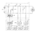
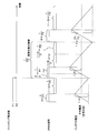
- FIG. 1 is a block diagram illustrating a configuration example of the voltage conversion device according to the first embodiment of the present invention
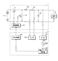
- FIG. 2 is a block diagram illustrating a functional configuration of the control unit 2 in the voltage conversion device.
- the voltage converter shown in FIG. 1 includes, for example, a DC / DC converter 1 that steps down the voltage of an external battery 3 and supplies the voltage to a load 4 and a control unit 2 that supplies a PWM signal to the DC / DC converter 1.
- the DC / DC converter 1 includes a switching element 11 having one end connected to the battery 3, a second switching element 12 and an inductor 13 each having one end connected to the other end of the switching element 11, and the other end of the inductor 13. And a capacitor 15 connected between the other end of the resistor 14 and the ground potential. The other end of the second switching element 12 is connected to the ground potential.
- the load 4 is connected across the capacitor 15.
- the switching element 11 and the second switching element 12 are, for example, N-channel MOSFETs each having one end as a drain.
- the DC / DC converter 1 also includes a drive circuit 16 that provides a drive signal for driving the switching element 11 and the second switching element 12 on / off.
- the drive circuit 16 supplies the PWM signal supplied from the control unit 2 and a PWM signal complementary to the PWM signal to the gates of the switching element 11 and the second switching element 12.
- the control unit 2 has a CPU 21, and the CPU 21 is connected to each other by a ROM 22 for storing information such as a program, a RAM 23 for storing temporarily generated information, and a timer 24 for measuring various times such as a PWM control cycle. Has been.
- the CPU 21 also includes a PWM circuit 25 that generates a PWM signal to be supplied to the drive circuit 16, and an A / D conversion circuit that detects the voltage across the resistor 14 and converts the current flowing through the resistor 14 into a digital current value. 26 and an A / D conversion circuit 27 for converting the voltage across the capacitor 15 into a digital voltage value are connected by a bus.
- control unit 2 realizes the function of the voltage loop controller 28 for controlling the output voltage output from the DC / DC converter 1 to the load 4 by a so-called voltage mode control method.
- the symbol “ ⁇ ” in the figure represents a subtractor.
- the voltage loop controller 28 is based on the deviation obtained by subtracting the digital voltage value Vo obtained by converting the output voltage output to the load 4 by the A / D conversion circuit 27 from the target voltage value Vref (ON time of the PWM signal ( Hereinafter, it is simply referred to as an on-time unless otherwise specified) and is output to the PWM circuit 25.
- the PWM circuit 25 generates a PWM signal having a duty ratio corresponding to a given on time.
- switching with respect to the switching element 11 and the second switching element 12 is performed according to the magnitude of the output current to the load 4 so that the voltage conversion efficiency is good.
- the frequency is switched. For example, when the output current is 20 A or more, the switching frequency is 150 kHz, and when the output current is less than 20 A, the switching frequency is 100 kHz.
- the ON time calculated by the voltage loop controller 28 is also switched. However, unless the duty ratio is corrected, the duty ratio of the PWM signal generated by the PWM circuit 25 does not change (described later). The same applies to other embodiments and modified examples).
- switching of the switching frequency (hereinafter also simply referred to as switching) is performed by changing (hereinafter also referred to as correction) the waveform of the PWM signal immediately after switching of the switching frequency. Such variations in output voltage that occur later are suppressed.
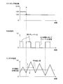
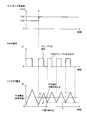
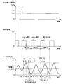
- FIG. 3 is a timing chart showing the relationship between the switching frequency, the PWM signal, and the inductor current according to the comparative example.
- FIG. 4 shows the relationship between the switching frequency, the PWM signal, and the inductor current according to the first embodiment of the present invention. It is a timing chart which shows. In each of the three timing diagrams shown in FIGS. 3 and 4, the horizontal axis is the same time axis.
- FIG. 3 shows a comparative example (conventional example) in which no change is made as in the present invention
- FIG. 4 shows an example according to the first embodiment of the present invention. In both examples, at timing A, the switching frequency is switched from 150 kHz to 100 kHz.
- the duty ratio in the PWM signal immediately after switching is the same as that before switching and is not changed. Therefore, the inductor current immediately after switching is increased, and the average value (represented by the broken line a) is higher than the average value in the steady state (represented by the solid line b). As a result, the output voltage varies greatly.
- a change in the inductor current accompanying switching of the switching frequency is predicted, and the lower limit value of the inductor current immediately after the switching is expressed as a lower limit value in a steady state (represented by a broken line c).
- the duty ratio in one cycle of the PWM signal immediately after switching is changed so as to coincide with (1).
- the lower limit value of the inductor current is matched between the cycle in which the duty ratio is changed and each cycle in the steady state after switching of the switching frequency.
- the amount of change in the waveform of the PWM signal immediately after the switching that is, the duty ratio after the change of the waveform immediately after switching the switching frequency (hereinafter simply referred to as “change”) and the specific value of the on-time after the change will be described. To do. Through a derivation process described later, it is derived that the changed duty ratio D ′ is calculated by the following equation (1).
- ON ′ ⁇ ON ⁇ F1 ⁇ (1-ON ⁇ F1) ⁇ / (2 ⁇ F1) + ⁇ ON ⁇ F1 ⁇ (1 + ON ⁇ F1) ⁇ / (2 ⁇ F2) (2)
- FIG. 5 is a timing chart showing the relationship between the switching frequency, the PWM signal, and the inductor current before and after switching of the switching frequency for explaining the derivation of the change amount.
- the horizontal axis in the figure represents time. The process of deriving the above equation (1) will be described with reference to FIG.
- T ⁇ represents a part of the on-time immediately after switching of the switching frequency.
- the absolute value of the slope of the inductor current decrease period can be regarded as D / (1-D) times the slope of the inductor current increase period. . That is, the length of the decrease period of the inductor current during the period in which the increase / decrease in the inductor current cancels becomes (1 ⁇ D) / D times the length of the increase period of the inductor current. Is obtained by the following equation (3).
- D ′ Since the changed duty ratio D ′ is represented by on time / period, that is, on time ⁇ frequency, D ′ is obtained by the following equation (4).
- T ⁇ ⁇ D (1 + D ) / 2 ⁇ ⁇ (1 / F2) - (D 2/2) ⁇ (1 / F1) ⁇ (5)
- D ′ [(D / 2) ⁇ (1 / F1) + ⁇ D (1 + D) / 2 ⁇ ⁇ (1 / F2) - (D 2/2) ⁇ (1 / F1) ]
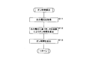
- FIG. 6 is a flowchart showing an operation procedure of the voltage converter.
- the operation shown in FIG. 6 is performed every control cycle of PWM control, and is executed by the CPU 21 in accordance with a control program stored in the ROM 22 in advance.
- step S1 In the operation of the voltage converter, the on-time calculation process (step S1), which is feedback control on the PWM signal based on the detected output voltage, and the necessity of switching of the switching frequency are determined. And a frequency switching process (step S2) in which the change amount is calculated and switched, and the CPU 21 executes these processes.
- step S1 the on-time calculation process (step S1) and the frequency switching process (step S2) will be described in detail.
- FIG. 7 is a flowchart showing the operation procedure of the on-time calculation process performed by the CPU 21 (subroutine of step S1).
- the CPU21 acquires the digital voltage value which converted the output voltage output to the load 4 with the A / D conversion circuit 27 (step S11). Next, the CPU 21 calculates the ON time by performing PID calculation so that the output voltage becomes the target voltage value (Vref) based on the acquired voltage value (Vo) of the output voltage (step S12). The CPU 21 sends the calculated on-time to the PWM circuit 25 (step S13) and ends the process. A PWM signal is generated in the PWM circuit 25 in accordance with the transmitted on-time.
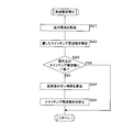
- FIG. 8 is a flowchart showing the operation procedure of the frequency switching process performed by the CPU 21 (subroutine of step S2).
- the CPU 21 obtains a digital current value obtained by converting the output current output to the load 4 by the A / D conversion circuit 26 (step S21).
- CPU21 specifies the switching frequency suitable for the electric current value of the acquired output current (step S22). Specifically, the CPU 21 specifies the switching frequency as 150 kHz when the acquired current value is 20 A or more, and specifies the switching frequency as 100 kHz when the acquired current value is less than 20 A.
- the CPU 21 determines whether or not the identified switching frequency matches the current switching frequency (step S23). If they match (S23: YES), the CPU 21 ends the process.
- the CPU 21 follows the above-described equation (2), the ON time before the change, the current switching frequency (the switching frequency before the change), and the specified switching frequency (the change The on-time after the change is calculated using (switching frequency after) (step S24). Then, the CPU 21 switches the current switching frequency to the specified switching frequency (step S25), and ends the process.
- the on-time in the first period immediately after switching of the switching frequency of the PWM signal is the on-time calculated in step S24.
- the characteristics of the waveform of the PWM signal immediately after switching (on time or duty ratio) ) Can be suppressed, so that the increase in the average value of the inductor current after switching due to switching can be suppressed, and as a result, fluctuations in output voltage can be suppressed and the constant voltage can be stabilized. It is possible to output to the load 4.
- the first embodiment is a mode in which the switching frequency is switched to decrease from a high frequency to a low frequency
- the first modification is a mode in which the switching frequency is switched to increase from a low frequency to a high frequency.
- the modification 1 of 1st Embodiment of this invention is demonstrated.
- the configuration of the voltage conversion device according to Modification 1 is the same as the configuration of the voltage conversion device according to the first embodiment described above (FIGS. 1 and 2).
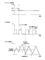
- FIG. 9 is a timing chart showing a relationship among the switching frequency, the PWM signal, and the inductor current according to the first modification.
- the same time axis is taken as the horizontal axis.
- the switching frequency is switched from 100 kHz to 150 kHz.
- a change in the inductor current accompanying switching of the switching frequency is predicted so that the lower limit value of the inductor current immediately after the switching coincides with the lower limit value in the steady state (represented by a broken line c).
- the duty ratio in one cycle of the PWM signal immediately after switching is changed.
- the lower limit value of the inductor current is matched between the cycle in which the duty ratio is changed and each cycle in the steady state after switching of the switching frequency.
- the ON time in one cycle of the PWM signal immediately after switching of the switching frequency is changed.
- the ON time in one cycle of the PWM signal immediately before switching of the switching frequency is changed.
- This second embodiment is suitable when PWM control is to be performed without special correction immediately after switching the switching frequency.
- FIG. 10 is a timing chart showing the relationship among the switching frequency, the PWM signal, and the inductor current according to the second embodiment of the present invention.
- the switching frequency is switched from 150 kHz to 100 kHz at timing A.
- the change in the inductor current accompanying switching of the switching frequency is predicted so that the lower limit value of the inductor current at the time of switching coincides with the lower limit value in the steady state (represented by a broken line c).
- the duty ratio in one cycle of the PWM signal immediately before switching is changed.
- the lower limit value of the inductor current is matched between the cycle in which the duty ratio is changed and each cycle in the steady state after switching of the switching frequency.
- correction is performed so that the duty ratio is smaller in one cycle of the PWM signal immediately before switching than in the previous cycle (that is, in each cycle after switching). Therefore, the inductor current in one cycle immediately before switching becomes small, and the average value (represented by a broken line d) is appropriately lowered with respect to the average value in a steady state (represented by a solid line e). As a result, an increase in the average value of the inductor current after switching is suppressed, and fluctuations in the output voltage after switching are suppressed.
- the change amount of the waveform in the PWM signal immediately before switching that is, the duty ratio after changing the waveform immediately before switching the switching frequency and the specific value of the ON time after changing will be described.
- the changed duty ratio D ′ is calculated by the following equation (6).
- ON ′ ⁇ ON ⁇ F1 ⁇ (3-ON ⁇ F1) ⁇ / (2 ⁇ F1) + ⁇ ON ⁇ F1 ⁇ (ON ⁇ F1-1) ⁇ / (2 ⁇ F2) (7)
- FIG. 11 is a timing chart showing the relationship between the switching frequency, the PWM signal, and the inductor current before and after switching of the switching frequency for explaining the derivation of the change amount.
- the horizontal axis in the figure represents time. The process of deriving the above calculation formula will be described with reference to FIG.
- the length of the inductor current decrease period during the period in which the increase / decrease in the inductor current cancels out is calculated as follows. Since the length of the increase period is (1 ⁇ D) / D times, the period 1 / F1 immediately before the switching is obtained by the following equation (8).
- D ′ is represented by on-time ⁇ frequency
- D ′ is obtained by the following equation (4) (re-displayed).
- T ⁇ ⁇ D (2-D) / 2 ⁇ ⁇ (1 / F1) + ⁇ D (D ⁇ 1) / 2 ⁇ ⁇ (1 / F2) ⁇ ⁇ ⁇ ⁇ ⁇ ⁇ ⁇ ⁇ ⁇ ⁇ ⁇ ⁇ ⁇ ⁇ ⁇ ⁇ ⁇ ⁇ ⁇ ⁇ ⁇ ⁇ ⁇ ⁇ ⁇ ⁇ ⁇ ⁇ ⁇ ⁇ ⁇ ⁇ ⁇ ⁇ ⁇ ⁇ ⁇ (9)
- D ′ [(D / 2) ⁇ (1 / F1) + ⁇ D (2-D) / 2 ⁇ ⁇ (1 / F1) + ⁇ D (D-1) / 2 ⁇ ⁇ (1 / F2)]
- ⁇ F1 ⁇ D (3-D) / 2 * (1 / F1) + D (D-1) / 2 * (1 / F2) ⁇ * F1
- FIG. 12 is a flowchart showing the operation procedure of the frequency switching process performed by the CPU 21 (subroutine of step S2).
- the switching flag in the figure is a flag indicating whether or not it is a cycle for switching the switching frequency, and the initial value is set to 0 and stored in the RAM 23. Since the processing from step S31 to S34 shown in FIG. 12 is the same as the processing from step S21 to S24 shown in FIG. 8 in the first embodiment, the description thereof will be simplified.
- the CPU 21 determines whether or not the switching flag is set to 1 (step S30). When the switching flag is not set to 1 (S30: NO), the CPU 21 acquires the output current output to the load 4 (step S31), and specifies a switching frequency suitable for the acquired output current (step S32). ).
- the CPU 21 determines whether or not the identified switching frequency matches the current switching frequency (step S33). If they match (S33: YES), the process is terminated.
- step S34 calculates the changed on-time according to the above-described equation (7) (step S34), sets the switching flag to 1 (step S35), and performs the process. finish.
- step S30 If the switching flag is set to 1 in step S30 (S30: YES), the CPU 21 clears the switching flag to 0 (step S36), and then switches the current switching frequency to the specified switching frequency (step S30). S37) The process ends.
- the waveform characteristics (ON time or duty ratio) immediately before switching are switched. ) Can be suppressed, so that the increase in the average value of the inductor current after switching due to switching can be suppressed, and as a result, fluctuations in output voltage can be suppressed and the constant voltage can be stabilized. It is possible to output to the load 4.
- D ′ calculated by the expression (6) may be less than 0, but in that case, D ′ is not limited. A numerical value close to 0 may be used.
- Modification 2 The second embodiment is a mode in which the switching frequency is switched to be lowered from a high frequency to a low frequency, whereas the second modification is a mode in which the switching frequency is switched to be raised from a low frequency to a high frequency.
- Modification 2 of the second embodiment of the present invention will be described.
- the configuration of the voltage conversion device according to Modification 2 is the same as the configuration of the voltage conversion device according to the first embodiment described above (FIGS. 1 and 2).
- FIG. 13 is a timing chart showing a relationship among the switching frequency, the PWM signal, and the inductor current according to the second modification.
- the switching frequency is switched from 100 kHz to 150 kHz at timing A.
- the change in the inductor current accompanying switching of the switching frequency is predicted so that the lower limit value of the inductor current at the time of switching coincides with the lower limit value in the steady state (represented by a broken line c).
- the duty ratio in one cycle of the PWM signal immediately before switching is changed.
- the lower limit value of the inductor current is matched between the cycle in which the duty ratio is changed and each cycle in the steady state after switching of the switching frequency.
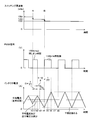
- FIG. 14 is a timing chart showing the relationship among the switching frequency, the PWM signal, and the inductor current according to the third embodiment of the present invention.
- the same time axis is taken as the horizontal axis.
- the switching frequency is switched from 150 kHz to 100 kHz at timing A.
- the on-time is changed over two cycles immediately after switching of the switching frequency. That is, in the first cycle immediately after switching the switching frequency, the on-time is changed by x1 ⁇ s so that the upper limit value of the inductor current matches the upper limit value in the steady state, and in the second cycle, the lower limit value of the inductor current is steady.
- the on-time is changed by x2 ⁇ s so as to coincide with the lower limit value in the state, and normal control is performed from the third period onward.
- the upper limit value and the lower limit value of the inductor current are made to coincide with each other in the first period and the second period in which the duty ratio is changed and in each period in the steady state after switching the switching frequency.
- the time when the switching frequency is switched is t0, and the time when the inductor current coincides with the average current immediately after that is t1.
- the time when the inductor current sequentially matches the average current is set as t3, t5, t7, t9, t11, and the time when the maximum value and the minimum value are sequentially set is set as t2, t4, t6, t8, t10, t12.
- the time from time t1 to t2 corresponds to T ⁇ in FIG. 5, and the time from time t8 to t10 corresponds to D ⁇ 1 / F2 in FIG.
- the following equation (10) is established.
- the changed duty ratio D ′ is represented by the on-time ⁇ frequency, so that D ′ is obtained by the following equation (4) (reprinted).
- the duty ratio D ′ in the first cycle (from time t0 to t4) after switching of the switching frequency is obtained as the following equation (11).
- the amount of correction of the on time of the PWM signal from time t0 to t2 is obtained by multiplying the second term on the right-hand side modified last by the equation (11) by the period (1 / F2). It is.
- the switching frequency from 150 kHz to 100 kHz, that is, when F2 / F1 is smaller than 1
- the duty ratio immediately after switching is corrected so as to be smaller than before switching.
- x1 is a negative number
- the PWM signal ON time immediately after switching is corrected so as to be shorter than the ON time in the steady state after switching.
- the correction amount of the PWM signal in the second period (from time t4 to t8) after switching of the switching frequency will be described.
- the duty ratio D ′ is corrected to be smaller than D as shown in the equation (11), so that the time from time t2 to t4 is the normal control at the frequency F2. It becomes longer than the time from time t10 to t12, and the inductor current is further reduced by that amount.
- the time from time t3 to t4 in the first cycle is T3, the time from time t0 to t1 is (D / 2) ⁇ (1 / F1), as in FIG. Further, the time from the time t1 to the time t3 is (1/2) ⁇ (1 / F2) corresponding to a half of one cycle similarly to the time from the time t9 to the time t11. Since the time from time t0 to t4 is 1 / F2, T3 is obtained by the following equation (12).
- the time from time t5 to t6 in the second period is T ⁇ .
- the length of the decrease period of the inductor current during the period in which the increase / decrease in the inductor current cancels can be regarded as (1-D) / D times the length of the increase period of the inductor current.
- the time from time t4 to t5 is D / (1-D) times T3
- the time from time t6 to t7 is (1-D) / D times T ⁇ .
- the time from time t7 to t8 is ⁇ (1-D) / 2 ⁇ ⁇ (1 / F2), the following equation (13) is established for the entire time of the second period.
- 1 / F2 T3 ⁇ D / (1-D) + T ⁇ + ⁇ (1-D) / D ⁇ ⁇ T ⁇ + ⁇ (1-D) / 2 ⁇ ⁇ (1 / F2) (13)
- the changed duty ratio D ′′ is obtained by the following equation (14).
- the changed duty ratio D ′′ is expressed by the following equation (16):
- the description of the intermediate result of the transformation of the formula is omitted, and the second term on the right-hand side last transformed in the formula (16) is multiplied by the period (1 / F2) to obtain the time t4 to t6.
- the correction amount of the PWM signal up to (corresponding to the above x2 ⁇ s)
- the duty ratio in the second cycle after switching is In this case, x2 is a positive number, and the ON time of the PWM signal in the second cycle after switching is longer than the ON time of each cycle in the steady state after switching. It is corrected to.
- the transition of the inductor current after switching the switching frequency is assumed, and the upper limit value or lower limit value of the inductor current is the steady state based on the assumed result. What is necessary is just to calculate similarly to 3rd Embodiment mentioned above using the switching frequency before switching, the switching frequency after switching, and the duty ratio before change so that it may correspond to the upper limit value or lower limit value.
- D ′ may be set to a value as close to 1 as possible, and D ′′ may be set to D, for example.
- the fourth embodiment of the present invention will be described below.
- the configuration of the voltage conversion device according to the fourth embodiment is the same as the configuration of the voltage conversion device according to the first embodiment described above (FIGS. 1 and 2).
- the third embodiment described above is a form in which the length of the ON signal of the PWM signal is corrected over two periods immediately after switching of the switching frequency, whereas the fourth embodiment is performed over two periods immediately before switching of the switching frequency. In this embodiment, the length of the ON signal of the PWM signal is corrected.
- FIG. 15 is a timing chart showing the relationship among the switching frequency, the PWM signal, and the inductor current according to the fourth embodiment of the present invention.
- the switching frequency is switched from 150 kHz to 100 kHz at timing A.
- the on-time is changed over two cycles of the PWM signal immediately before switching. That is, in the first period (from time t0 to t4) of the two periods immediately before the switching of the switching frequency, the on-time is changed by y1 ⁇ s so that the upper limit value of the inductor current matches the upper limit value in the steady state.
- the on-time is changed by y2 ⁇ s so that the lower limit value of the inductor current matches the lower limit value in the steady state, and normal control is performed immediately after switching.
- the upper limit value and the lower limit value of the inductor current are made to coincide with each other in the first period and the second period in which the duty ratio is changed and in each period in the steady state after switching the switching frequency.
- the time two cycles before the switching frequency is set to t0, and immediately after that, the time when the inductor current matches the average current is set to t1.
- the time when the inductor current sequentially matches the average current is set as t3, t5, t7, t9, t11, and the time when the maximum value and the minimum value are sequentially set is set as t2, t4, t6, t8, t10, t12.
- the time for switching the switching frequency is t8.
- the time from time t1 to t2 corresponds to T ⁇ in FIG. 5, and the time from time t8 to t10 corresponds to D ⁇ 1 / F2 in FIG.
- the following equation (10) (repost) is established.
- the changed duty ratio D ′ is represented by ON time ⁇ frequency, and therefore D ′ is obtained by the following equation (17).
- the duty ratio D ′ in the first cycle among the two cycles immediately before the switching of the switching frequency is obtained as the following equation (18).
- the PWM signal correction amount (corresponding to y1 ⁇ s described above) from time t0 to t2 is obtained by multiplying the second term on the right side modified last by the equation (18) by the period (1 / F1).
- the switching frequency from 150 kHz to 100 kHz, that is, when F1 / F2 is greater than 1
- the duty ratio of the first period out of the two periods immediately before switching is greater than the previous period (that is, each period after switching). It is corrected so that In this case, y1 is a positive number and is corrected so that the on-time of the PWM signal in the first period out of the two periods immediately before switching is longer than the on-time in the steady state after switching.
- T3 the time from time t0 to t1 is (D / 2) ⁇ (1 / F1). Further, the time from the time t1 to the time t3 is (1/2) ⁇ (1 / F2) corresponding to a half of one cycle similarly to the time from the time t9 to the time t11. Since the time from time t0 to t4 is 1 / F1, T3 is obtained by the following equation (19).
- the time from time t5 to t6 in the second period is T ⁇ .
- the length of the decrease period of the inductor current during the period in which the increase / decrease in the inductor current cancels can be regarded as (1-D) / D times the length of the increase period of the inductor current.
- the time from time t4 to t5 is D / (1-D) times T3
- the time from time t6 to t7 is (1-D) / D times T ⁇ .
- the time from time t7 to t8 is ⁇ (1-D) / 2 ⁇ ⁇ (1 / F1), the following equation (20) is established for the entire second period.
- the changed duty ratio is represented by the on time from time t4 to t6 divided by the period, that is, the on time x frequency, the changed duty ratio D "is obtained by the following equation (21).
- T ⁇ ⁇ D (1 + D) / 2 ⁇ ⁇ (1 / F1) ⁇ T3 ⁇ D 2 / (1-D) (22)
- the changed duty ratio D ′′ is expressed by the following equation (23):
- the description of the intermediate result of the transformation of the formula is omitted, and the second term on the right-hand side last transformed in the formula (23) is multiplied by the period (1 / F1) to obtain the time t4 to t6.
- PWM signal correction amount (corresponding to y2 ⁇ s above)
- the switching frequency from 150 kHz to 100 kHz, that is, when F1 / F2 is greater than F1
- the duty ratio of the first cycle of the two cycles immediately before switching In this case, y2 is a negative number, and the on-time of the PWM signal in the second period of the two periods immediately before the switching is corrected to be smaller than the previous period (ie, each period after the switching). But cut It is corrected to be shorter than the ON time in the steady state after e.
- the fluctuation of the output voltage is not in the increasing direction but in the decreasing direction. Therefore, when switching the switching frequency, there is no possibility of exceeding the upper limit voltage indicated in the specification.
- D ′ may be set to a value as close to 1 as possible, and D ′′ may be set to D, for example.
- the fifth embodiment of the present invention will be described below.
- the configuration of the voltage conversion device according to the fifth embodiment is the same as the configuration of the voltage conversion device according to the first embodiment described above (FIGS. 1 and 2).
- the ON time in one cycle of the PWM signal immediately after switching of the switching frequency is changed, but in the fifth embodiment, the frequency in one cycle of the PWM signal immediately after switching of the switching frequency is changed.
- the fifth embodiment can also be regarded as a form of changing the frequency in one cycle of the PWM signal immediately before switching the switching frequency.
- FIG. 16 is a timing chart showing the relationship among the switching frequency, the PWM signal, and the inductor current according to the fifth embodiment of the present invention.
- the switching frequency is switched at timing A (or timing B).
- the frequency of the PWM signal is set to, for example, 120 kHz without changing the ON time for only one period immediately after switching of the switching frequency (or immediately before switching), for example, after the second period (or after switching).
- the frequency of the PWM signal is 100 kHz.
- the frequency of the PWM signal is changed.
- the lower limit value of the inductor current is matched between the period in which the frequency of the PWM signal is changed and each period in the steady state after switching of the switching frequency.
- the time when the switching frequency is switched is t0 (or t4), and the time when the inductor current coincides with the average current immediately after time t0 is t1.
- the time when the inductor current sequentially matches the average current is set to t3, t5, and t7, and the time when the maximum value and the minimum value are sequentially set are set to t2, t4, t6, and t8.
- the time from time t0 to t2 corresponds to D ⁇ (1 / F1) before switching of the switching frequency in FIG. Further, the time from time t2 to t3 corresponds to half of (1-D) ⁇ (1 / F1) before switching of the switching frequency in FIG.
- the time from time t0 to t4 is 1 / F2. Therefore, if the time from time t3 to t4 is T3, T3 is obtained by the following equation (24).
- T3 (1 / F2) ⁇ D ⁇ (1 / F1) - ⁇ (1-D) / 2 ⁇ x (1 / F1) (24)
- the depth of the valley of the inductor current at time t4 (the difference between the average current and the minimum value) is the inductor current at time t8. It is the same as the depth of the valley. The depths of these valleys are the same as the peak height of the inductor current (difference between the average current and the maximum value) at time t6.
- the switching frequency after the second period after switching is F3
- the ratio of the peak height at time t6 to the peak height of the inductor current at time t2 is the ratio of F1 to F3. Therefore, the ratio of T3 to the time from time t2 to time t3 becomes equal to the ratio of F1 to F3, and the following equation (25) is established.
- This F2 may be a switching frequency of one cycle immediately after switching of switching frequency (or immediately before switching).
- F2 2 ⁇ F1 ⁇ F3 / ⁇ (1-D) ⁇ F1 + (1 + D) ⁇ F3 ⁇ (26)
- each PWM immediately before and immediately after switching of the switching frequency is changed.
- the ON time in one cycle of the signal is changed.
- the sixth embodiment is suitable when the feedback control based on the output voltage is not performed for each cycle of the PWM signal.
- FIG. 17 is a timing chart showing the relationship among the switching frequency, the PWM signal, and the inductor current according to the sixth embodiment of the present invention.
- the switching frequency is switched from 150 kHz to 100 kHz at timing A.
- the change in the inductor current accompanying the switching of the switching frequency is predicted, and the minimum value of the inductor current at the end of one cycle immediately after the switching is the lower limit value in the steady state (represented by the broken line c).
- the duty ratio in one cycle of the PWM signal immediately before switching and immediately after switching is changed so as to substantially match.
- the lower limit value of the inductor current is substantially matched between the second period in which the duty ratio is changed and each period in the steady state after switching of the switching frequency.
- the duty ratio is higher than each cycle in the steady state in one cycle of the PWM signal immediately before switching and immediately after switching. Correct to be smaller (or larger).
- the average value of the inductor current in one cycle before switching and immediately after switching is appropriately lowered (or increased), so that the lower limit value of the inductor current in one cycle immediately after the change of the duty ratio and the steady state after switching.
- the duty ratio D_ after the change is the duty ratio D before the change and the D ′ (the corrected duty ratio when the switching frequency is corrected before or after the switching frequency is changed by the expression (1) or (6)) ) Is calculated by the following equation (27) or (28).
- D _ [D + ⁇ D (1-D) / 2 ⁇ (1 / F1) + D (1 + D) / 2 ⁇ (1 / F2) ⁇ ⁇ F1] / 2 (27)
- D _ [D + ⁇ D (3-D) / 2 ⁇ (1 / F1) + D (D-1) / 2 ⁇ (1 / F2) ⁇ ⁇ F1] / 2 (28)
- ON _ [ON ⁇ F1 + ⁇ ON ⁇ F1 ⁇ (1-ON ⁇ F1) ⁇ / (2 ⁇ F1) + ⁇ ON ⁇ F1 ⁇ (1 + ON ⁇ F1) ⁇ / (2 ⁇ F2) (29)
- ON _ [ON ⁇ F1 + ⁇ ON ⁇ F1 ⁇ (3-ON ⁇ F1) ⁇ / (2 ⁇ F1) + ⁇ ON ⁇ F1 ⁇ (ON ⁇ F1-1) ⁇ / (2 ⁇ F2) (30)
- the duty ratio D_ of the PWM signal immediately before and after switching is calculated by the arithmetic average of D and D ′.
- the geometric average of D and D ′, or D and D ′ D_ may be calculated based on an average value of.
- the frequency was changed without changing the on-time immediately after switching of the switching frequency (or immediately before switching), but as a form combining the first (or second) and fifth embodiments, Immediately after switching the switching frequency (or just before switching), the on-time and frequency are changed at the same time, and the lower limit value of the inductor current is made uniform immediately after changing the PWM signal waveform and in the steady state after switching the switching frequency. Is possible.
- the switching frequency is switched from 150 kHz to 100 kHz or from 100 kHz to 150 kHz according to the magnitude of the output current
- the present invention can be similarly applied to a case where the switching frequency is switched from 125 kHz to 110 kHz or 110 kHz to 125 kHz. That is, regarding the numerical value of the switching frequency before and after switching according to the magnitude of the output current, the numerical value described in the specification is merely an example, and depending on the product form of the target voltage converter, any numerical value can be The present invention can cope with changes to numerical values.
- the DC / DC converter 1 may boost or step up or step down the voltage of the battery 3.
Landscapes
- Engineering & Computer Science (AREA)
- Power Engineering (AREA)
- Dc-Dc Converters (AREA)
Priority Applications (3)
| Application Number | Priority Date | Filing Date | Title |
|---|---|---|---|
| CN201780007599.3A CN108475986A (zh) | 2016-03-29 | 2017-03-13 | 电压转换装置及电压转换方法 |
| DE112017001741.6T DE112017001741T5 (de) | 2016-03-29 | 2017-03-13 | Spannungsumwandlungsvorrichtung und Spannungsumwandlungsverfahren |
| US16/085,004 US20190074821A1 (en) | 2016-03-29 | 2017-03-13 | Voltage conversion device and voltage conversion method |
Applications Claiming Priority (2)
| Application Number | Priority Date | Filing Date | Title |
|---|---|---|---|
| JP2016066759A JP2017184404A (ja) | 2016-03-29 | 2016-03-29 | 電圧変換装置及び電圧変換方法 |
| JP2016-066759 | 2016-03-29 |
Publications (1)
| Publication Number | Publication Date |
|---|---|
| WO2017169686A1 true WO2017169686A1 (ja) | 2017-10-05 |
Family
ID=59964193
Family Applications (1)
| Application Number | Title | Priority Date | Filing Date |
|---|---|---|---|
| PCT/JP2017/009928 Ceased WO2017169686A1 (ja) | 2016-03-29 | 2017-03-13 | 電圧変換装置及び電圧変換方法 |
Country Status (5)
| Country | Link |
|---|---|
| US (1) | US20190074821A1 (enExample) |
| JP (1) | JP2017184404A (enExample) |
| CN (1) | CN108475986A (enExample) |
| DE (1) | DE112017001741T5 (enExample) |
| WO (1) | WO2017169686A1 (enExample) |
Families Citing this family (2)
| Publication number | Priority date | Publication date | Assignee | Title |
|---|---|---|---|---|
| CN108667283A (zh) | 2018-06-11 | 2018-10-16 | 矽力杰半导体技术(杭州)有限公司 | 一种用于降低thd的控制方法及系统 |
| JP7181805B2 (ja) * | 2019-02-12 | 2022-12-01 | 株式会社三社電機製作所 | 半導体素子の過渡熱抵抗測定用電源回路 |
Citations (3)
| Publication number | Priority date | Publication date | Assignee | Title |
|---|---|---|---|---|
| JP2013247574A (ja) * | 2012-05-28 | 2013-12-09 | Renesas Electronics Corp | Pwm信号生成回路および半導体装置 |
| JP2014161190A (ja) * | 2013-02-20 | 2014-09-04 | Fujitsu Ltd | 制御装置、制御方法および電源装置 |
| JP2015211539A (ja) * | 2014-04-25 | 2015-11-24 | ローム株式会社 | スイッチング電源の制御回路およびそれを用いた電源回路、ならびに電子機器および基地局、半導体集積回路 |
Family Cites Families (2)
| Publication number | Priority date | Publication date | Assignee | Title |
|---|---|---|---|---|
| JPH10323027A (ja) | 1997-05-19 | 1998-12-04 | Kyocera Corp | 電源回路 |
| JP2016066759A (ja) | 2014-09-25 | 2016-04-28 | 山本化成株式会社 | 有機トランジスタ |
-
2016
- 2016-03-29 JP JP2016066759A patent/JP2017184404A/ja active Pending
-
2017
- 2017-03-13 US US16/085,004 patent/US20190074821A1/en not_active Abandoned
- 2017-03-13 WO PCT/JP2017/009928 patent/WO2017169686A1/ja not_active Ceased
- 2017-03-13 CN CN201780007599.3A patent/CN108475986A/zh active Pending
- 2017-03-13 DE DE112017001741.6T patent/DE112017001741T5/de not_active Withdrawn
Patent Citations (3)
| Publication number | Priority date | Publication date | Assignee | Title |
|---|---|---|---|---|
| JP2013247574A (ja) * | 2012-05-28 | 2013-12-09 | Renesas Electronics Corp | Pwm信号生成回路および半導体装置 |
| JP2014161190A (ja) * | 2013-02-20 | 2014-09-04 | Fujitsu Ltd | 制御装置、制御方法および電源装置 |
| JP2015211539A (ja) * | 2014-04-25 | 2015-11-24 | ローム株式会社 | スイッチング電源の制御回路およびそれを用いた電源回路、ならびに電子機器および基地局、半導体集積回路 |
Also Published As
| Publication number | Publication date |
|---|---|
| JP2017184404A (ja) | 2017-10-05 |
| CN108475986A (zh) | 2018-08-31 |
| DE112017001741T5 (de) | 2018-12-13 |
| US20190074821A1 (en) | 2019-03-07 |
Similar Documents
| Publication | Publication Date | Title |
|---|---|---|
| JP6350305B2 (ja) | 電圧変換装置及び電圧変換方法 | |
| EP2466740B1 (en) | Circuit of high efficient buck-boost switching regulator and control method thereof | |
| JP5930700B2 (ja) | スイッチング電源装置及びその制御方法 | |
| US9146571B2 (en) | Power converter with average current limiting | |
| TWI430552B (zh) | 連續地切換之升-降壓控制 | |
| US20120086418A1 (en) | Multi-phase switching regulator and driver circuit and control method thereof | |
| JP6203688B2 (ja) | 電源回路とその制御方法 | |
| KR20130036065A (ko) | 벅 스위치 모드 파워 컨버터 큰 신호 천이 응답 최적화기 | |
| CN113098281A (zh) | 一种应用于准并联结构变换器的变占空比软启动控制系统 | |
| JP2017060303A (ja) | 電源装置 | |
| JP6013294B2 (ja) | 電力変換装置 | |
| US8675375B2 (en) | System and method for input voltage transient response control | |
| JP6070715B2 (ja) | 電力変換装置 | |
| WO2017169686A1 (ja) | 電圧変換装置及び電圧変換方法 | |
| JP4937895B2 (ja) | 昇降圧コンバータの駆動制御装置 | |
| JP2017184404A5 (enExample) | ||
| JP2018085827A (ja) | 電圧制御装置 | |
| JP6144374B1 (ja) | 電力変換装置 | |
| EP3203620B1 (en) | Dc-dc converter including dynamically adjusted duty cycle limit | |
| US20180235063A1 (en) | Device and method for processing an inductor current | |
| JP5388912B2 (ja) | パルス電源装置とそのパルス電圧生成方法 | |
| JP6316392B2 (ja) | Dc/dcコンバータ | |
| KR101299474B1 (ko) | 전력변환장치 | |
| JP2016149881A (ja) | 直流−直流変換器の制御装置および制御方法 | |
| JP2023161414A (ja) | Dc-dcコンバータ |
Legal Events
| Date | Code | Title | Description |
|---|---|---|---|
| 121 | Ep: the epo has been informed by wipo that ep was designated in this application |
Ref document number: 17774230 Country of ref document: EP Kind code of ref document: A1 |
|
| 122 | Ep: pct application non-entry in european phase |
Ref document number: 17774230 Country of ref document: EP Kind code of ref document: A1 |