WO2017169637A1 - 液晶硬化フィルム及びその製造方法 - Google Patents
液晶硬化フィルム及びその製造方法 Download PDFInfo
- Publication number
- WO2017169637A1 WO2017169637A1 PCT/JP2017/009542 JP2017009542W WO2017169637A1 WO 2017169637 A1 WO2017169637 A1 WO 2017169637A1 JP 2017009542 W JP2017009542 W JP 2017009542W WO 2017169637 A1 WO2017169637 A1 WO 2017169637A1
- Authority
- WO
- WIPO (PCT)
- Prior art keywords
- group
- liquid crystal
- carbon atoms
- crystal cured
- cured layer
- Prior art date
- Legal status (The legal status is an assumption and is not a legal conclusion. Google has not performed a legal analysis and makes no representation as to the accuracy of the status listed.)
- Ceased
Links
- 0 C**[*@@](*)C(*)=NN(*)* Chemical compound C**[*@@](*)C(*)=NN(*)* 0.000 description 10
- RHOOLJLEYYXKTK-UHFFFAOYSA-N Cc1cnc(C)nc1 Chemical compound Cc1cnc(C)nc1 RHOOLJLEYYXKTK-UHFFFAOYSA-N 0.000 description 1
- BGVTUIRPHLSMJU-UHFFFAOYSA-N Cc1nnc(C)cc1 Chemical compound Cc1nnc(C)cc1 BGVTUIRPHLSMJU-UHFFFAOYSA-N 0.000 description 1
Images

Classifications
-
- C—CHEMISTRY; METALLURGY
- C09—DYES; PAINTS; POLISHES; NATURAL RESINS; ADHESIVES; COMPOSITIONS NOT OTHERWISE PROVIDED FOR; APPLICATIONS OF MATERIALS NOT OTHERWISE PROVIDED FOR
- C09K—MATERIALS FOR MISCELLANEOUS APPLICATIONS, NOT PROVIDED FOR ELSEWHERE
- C09K19/00—Liquid crystal materials
- C09K19/04—Liquid crystal materials characterised by the chemical structure of the liquid crystal components, e.g. by a specific unit
- C09K19/38—Polymers
-
- C—CHEMISTRY; METALLURGY
- C09—DYES; PAINTS; POLISHES; NATURAL RESINS; ADHESIVES; COMPOSITIONS NOT OTHERWISE PROVIDED FOR; APPLICATIONS OF MATERIALS NOT OTHERWISE PROVIDED FOR
- C09K—MATERIALS FOR MISCELLANEOUS APPLICATIONS, NOT PROVIDED FOR ELSEWHERE
- C09K19/00—Liquid crystal materials
- C09K19/04—Liquid crystal materials characterised by the chemical structure of the liquid crystal components, e.g. by a specific unit
- C09K19/06—Non-steroidal liquid crystal compounds
- C09K19/34—Non-steroidal liquid crystal compounds containing at least one heterocyclic ring
- C09K19/3491—Non-steroidal liquid crystal compounds containing at least one heterocyclic ring having sulfur as hetero atom
- C09K19/3497—Non-steroidal liquid crystal compounds containing at least one heterocyclic ring having sulfur as hetero atom the heterocyclic ring containing sulfur and nitrogen atoms
-
- C—CHEMISTRY; METALLURGY
- C09—DYES; PAINTS; POLISHES; NATURAL RESINS; ADHESIVES; COMPOSITIONS NOT OTHERWISE PROVIDED FOR; APPLICATIONS OF MATERIALS NOT OTHERWISE PROVIDED FOR
- C09K—MATERIALS FOR MISCELLANEOUS APPLICATIONS, NOT PROVIDED FOR ELSEWHERE
- C09K19/00—Liquid crystal materials
- C09K19/04—Liquid crystal materials characterised by the chemical structure of the liquid crystal components, e.g. by a specific unit
-
- C—CHEMISTRY; METALLURGY
- C09—DYES; PAINTS; POLISHES; NATURAL RESINS; ADHESIVES; COMPOSITIONS NOT OTHERWISE PROVIDED FOR; APPLICATIONS OF MATERIALS NOT OTHERWISE PROVIDED FOR
- C09K—MATERIALS FOR MISCELLANEOUS APPLICATIONS, NOT PROVIDED FOR ELSEWHERE
- C09K19/00—Liquid crystal materials
- C09K19/52—Liquid crystal materials characterised by components which are not liquid crystals, e.g. additives with special physical aspect: solvents, solid particles
- C09K19/54—Additives having no specific mesophase characterised by their chemical composition
-
- G—PHYSICS
- G02—OPTICS
- G02B—OPTICAL ELEMENTS, SYSTEMS OR APPARATUS
- G02B5/00—Optical elements other than lenses
- G02B5/30—Polarising elements
-
- G—PHYSICS
- G02—OPTICS
- G02F—OPTICAL DEVICES OR ARRANGEMENTS FOR THE CONTROL OF LIGHT BY MODIFICATION OF THE OPTICAL PROPERTIES OF THE MEDIA OF THE ELEMENTS INVOLVED THEREIN; NON-LINEAR OPTICS; FREQUENCY-CHANGING OF LIGHT; OPTICAL LOGIC ELEMENTS; OPTICAL ANALOGUE/DIGITAL CONVERTERS
- G02F1/00—Devices or arrangements for the control of the intensity, colour, phase, polarisation or direction of light arriving from an independent light source, e.g. switching, gating or modulating; Non-linear optics
- G02F1/01—Devices or arrangements for the control of the intensity, colour, phase, polarisation or direction of light arriving from an independent light source, e.g. switching, gating or modulating; Non-linear optics for the control of the intensity, phase, polarisation or colour
- G02F1/13—Devices or arrangements for the control of the intensity, colour, phase, polarisation or direction of light arriving from an independent light source, e.g. switching, gating or modulating; Non-linear optics for the control of the intensity, phase, polarisation or colour based on liquid crystals, e.g. single liquid crystal display cells
- G02F1/133—Constructional arrangements; Operation of liquid crystal cells; Circuit arrangements
- G02F1/1333—Constructional arrangements; Manufacturing methods
- G02F1/1335—Structural association of cells with optical devices, e.g. polarisers or reflectors
- G02F1/133528—Polarisers
-
- G—PHYSICS
- G02—OPTICS
- G02F—OPTICAL DEVICES OR ARRANGEMENTS FOR THE CONTROL OF LIGHT BY MODIFICATION OF THE OPTICAL PROPERTIES OF THE MEDIA OF THE ELEMENTS INVOLVED THEREIN; NON-LINEAR OPTICS; FREQUENCY-CHANGING OF LIGHT; OPTICAL LOGIC ELEMENTS; OPTICAL ANALOGUE/DIGITAL CONVERTERS
- G02F1/00—Devices or arrangements for the control of the intensity, colour, phase, polarisation or direction of light arriving from an independent light source, e.g. switching, gating or modulating; Non-linear optics
- G02F1/01—Devices or arrangements for the control of the intensity, colour, phase, polarisation or direction of light arriving from an independent light source, e.g. switching, gating or modulating; Non-linear optics for the control of the intensity, phase, polarisation or colour
- G02F1/13—Devices or arrangements for the control of the intensity, colour, phase, polarisation or direction of light arriving from an independent light source, e.g. switching, gating or modulating; Non-linear optics for the control of the intensity, phase, polarisation or colour based on liquid crystals, e.g. single liquid crystal display cells
- G02F1/133—Constructional arrangements; Operation of liquid crystal cells; Circuit arrangements
- G02F1/1333—Constructional arrangements; Manufacturing methods
- G02F1/1335—Structural association of cells with optical devices, e.g. polarisers or reflectors
- G02F1/13363—Birefringent elements, e.g. for optical compensation
-
- G—PHYSICS
- G02—OPTICS
- G02F—OPTICAL DEVICES OR ARRANGEMENTS FOR THE CONTROL OF LIGHT BY MODIFICATION OF THE OPTICAL PROPERTIES OF THE MEDIA OF THE ELEMENTS INVOLVED THEREIN; NON-LINEAR OPTICS; FREQUENCY-CHANGING OF LIGHT; OPTICAL LOGIC ELEMENTS; OPTICAL ANALOGUE/DIGITAL CONVERTERS
- G02F1/00—Devices or arrangements for the control of the intensity, colour, phase, polarisation or direction of light arriving from an independent light source, e.g. switching, gating or modulating; Non-linear optics
- G02F1/01—Devices or arrangements for the control of the intensity, colour, phase, polarisation or direction of light arriving from an independent light source, e.g. switching, gating or modulating; Non-linear optics for the control of the intensity, phase, polarisation or colour
- G02F1/13—Devices or arrangements for the control of the intensity, colour, phase, polarisation or direction of light arriving from an independent light source, e.g. switching, gating or modulating; Non-linear optics for the control of the intensity, phase, polarisation or colour based on liquid crystals, e.g. single liquid crystal display cells
- G02F1/133—Constructional arrangements; Operation of liquid crystal cells; Circuit arrangements
- G02F1/1333—Constructional arrangements; Manufacturing methods
- G02F1/1335—Structural association of cells with optical devices, e.g. polarisers or reflectors
- G02F1/13363—Birefringent elements, e.g. for optical compensation
- G02F1/133634—Birefringent elements, e.g. for optical compensation the refractive index Nz perpendicular to the element surface being different from in-plane refractive indices Nx and Ny, e.g. biaxial or with normal optical axis
-
- C—CHEMISTRY; METALLURGY
- C09—DYES; PAINTS; POLISHES; NATURAL RESINS; ADHESIVES; COMPOSITIONS NOT OTHERWISE PROVIDED FOR; APPLICATIONS OF MATERIALS NOT OTHERWISE PROVIDED FOR
- C09K—MATERIALS FOR MISCELLANEOUS APPLICATIONS, NOT PROVIDED FOR ELSEWHERE
- C09K19/00—Liquid crystal materials
- C09K19/04—Liquid crystal materials characterised by the chemical structure of the liquid crystal components, e.g. by a specific unit
- C09K2019/0444—Liquid crystal materials characterised by the chemical structure of the liquid crystal components, e.g. by a specific unit characterized by a linking chain between rings or ring systems, a bridging chain between extensive mesogenic moieties or an end chain group
- C09K2019/0448—Liquid crystal materials characterised by the chemical structure of the liquid crystal components, e.g. by a specific unit characterized by a linking chain between rings or ring systems, a bridging chain between extensive mesogenic moieties or an end chain group the end chain group being a polymerizable end group, e.g. -Sp-P or acrylate
-
- G—PHYSICS
- G02—OPTICS
- G02B—OPTICAL ELEMENTS, SYSTEMS OR APPARATUS
- G02B5/00—Optical elements other than lenses
- G02B5/30—Polarising elements
- G02B5/3025—Polarisers, i.e. arrangements capable of producing a definite output polarisation state from an unpolarised input state
- G02B5/3033—Polarisers, i.e. arrangements capable of producing a definite output polarisation state from an unpolarised input state in the form of a thin sheet or foil, e.g. Polaroid
-
- G—PHYSICS
- G02—OPTICS
- G02F—OPTICAL DEVICES OR ARRANGEMENTS FOR THE CONTROL OF LIGHT BY MODIFICATION OF THE OPTICAL PROPERTIES OF THE MEDIA OF THE ELEMENTS INVOLVED THEREIN; NON-LINEAR OPTICS; FREQUENCY-CHANGING OF LIGHT; OPTICAL LOGIC ELEMENTS; OPTICAL ANALOGUE/DIGITAL CONVERTERS
- G02F1/00—Devices or arrangements for the control of the intensity, colour, phase, polarisation or direction of light arriving from an independent light source, e.g. switching, gating or modulating; Non-linear optics
- G02F1/01—Devices or arrangements for the control of the intensity, colour, phase, polarisation or direction of light arriving from an independent light source, e.g. switching, gating or modulating; Non-linear optics for the control of the intensity, phase, polarisation or colour
- G02F1/13—Devices or arrangements for the control of the intensity, colour, phase, polarisation or direction of light arriving from an independent light source, e.g. switching, gating or modulating; Non-linear optics for the control of the intensity, phase, polarisation or colour based on liquid crystals, e.g. single liquid crystal display cells
- G02F1/133—Constructional arrangements; Operation of liquid crystal cells; Circuit arrangements
- G02F1/1333—Constructional arrangements; Manufacturing methods
- G02F1/1335—Structural association of cells with optical devices, e.g. polarisers or reflectors
- G02F1/133528—Polarisers
- G02F1/133541—Circular polarisers
-
- G—PHYSICS
- G02—OPTICS
- G02F—OPTICAL DEVICES OR ARRANGEMENTS FOR THE CONTROL OF LIGHT BY MODIFICATION OF THE OPTICAL PROPERTIES OF THE MEDIA OF THE ELEMENTS INVOLVED THEREIN; NON-LINEAR OPTICS; FREQUENCY-CHANGING OF LIGHT; OPTICAL LOGIC ELEMENTS; OPTICAL ANALOGUE/DIGITAL CONVERTERS
- G02F1/00—Devices or arrangements for the control of the intensity, colour, phase, polarisation or direction of light arriving from an independent light source, e.g. switching, gating or modulating; Non-linear optics
- G02F1/01—Devices or arrangements for the control of the intensity, colour, phase, polarisation or direction of light arriving from an independent light source, e.g. switching, gating or modulating; Non-linear optics for the control of the intensity, phase, polarisation or colour
- G02F1/13—Devices or arrangements for the control of the intensity, colour, phase, polarisation or direction of light arriving from an independent light source, e.g. switching, gating or modulating; Non-linear optics for the control of the intensity, phase, polarisation or colour based on liquid crystals, e.g. single liquid crystal display cells
- G02F1/133—Constructional arrangements; Operation of liquid crystal cells; Circuit arrangements
- G02F1/1333—Constructional arrangements; Manufacturing methods
- G02F1/1335—Structural association of cells with optical devices, e.g. polarisers or reflectors
- G02F1/133528—Polarisers
- G02F1/133543—Cholesteric polarisers
-
- G—PHYSICS
- G02—OPTICS
- G02F—OPTICAL DEVICES OR ARRANGEMENTS FOR THE CONTROL OF LIGHT BY MODIFICATION OF THE OPTICAL PROPERTIES OF THE MEDIA OF THE ELEMENTS INVOLVED THEREIN; NON-LINEAR OPTICS; FREQUENCY-CHANGING OF LIGHT; OPTICAL LOGIC ELEMENTS; OPTICAL ANALOGUE/DIGITAL CONVERTERS
- G02F1/00—Devices or arrangements for the control of the intensity, colour, phase, polarisation or direction of light arriving from an independent light source, e.g. switching, gating or modulating; Non-linear optics
- G02F1/01—Devices or arrangements for the control of the intensity, colour, phase, polarisation or direction of light arriving from an independent light source, e.g. switching, gating or modulating; Non-linear optics for the control of the intensity, phase, polarisation or colour
- G02F1/13—Devices or arrangements for the control of the intensity, colour, phase, polarisation or direction of light arriving from an independent light source, e.g. switching, gating or modulating; Non-linear optics for the control of the intensity, phase, polarisation or colour based on liquid crystals, e.g. single liquid crystal display cells
- G02F1/133—Constructional arrangements; Operation of liquid crystal cells; Circuit arrangements
- G02F1/1333—Constructional arrangements; Manufacturing methods
- G02F1/1335—Structural association of cells with optical devices, e.g. polarisers or reflectors
- G02F1/133528—Polarisers
- G02F1/133548—Wire-grid polarisers
-
- G—PHYSICS
- G02—OPTICS
- G02F—OPTICAL DEVICES OR ARRANGEMENTS FOR THE CONTROL OF LIGHT BY MODIFICATION OF THE OPTICAL PROPERTIES OF THE MEDIA OF THE ELEMENTS INVOLVED THEREIN; NON-LINEAR OPTICS; FREQUENCY-CHANGING OF LIGHT; OPTICAL LOGIC ELEMENTS; OPTICAL ANALOGUE/DIGITAL CONVERTERS
- G02F1/00—Devices or arrangements for the control of the intensity, colour, phase, polarisation or direction of light arriving from an independent light source, e.g. switching, gating or modulating; Non-linear optics
- G02F1/01—Devices or arrangements for the control of the intensity, colour, phase, polarisation or direction of light arriving from an independent light source, e.g. switching, gating or modulating; Non-linear optics for the control of the intensity, phase, polarisation or colour
- G02F1/13—Devices or arrangements for the control of the intensity, colour, phase, polarisation or direction of light arriving from an independent light source, e.g. switching, gating or modulating; Non-linear optics for the control of the intensity, phase, polarisation or colour based on liquid crystals, e.g. single liquid crystal display cells
- G02F1/133—Constructional arrangements; Operation of liquid crystal cells; Circuit arrangements
- G02F1/1333—Constructional arrangements; Manufacturing methods
- G02F1/1335—Structural association of cells with optical devices, e.g. polarisers or reflectors
- G02F1/13363—Birefringent elements, e.g. for optical compensation
- G02F1/133631—Birefringent elements, e.g. for optical compensation with a spatial distribution of the retardation value
Definitions
- R 4 represents an alkyl group having 1 to 20 carbon atoms, an alkenyl group having 2 to 20 carbon atoms, a phenyl group, or a 4-methylphenyl group.
- R 9 is an optionally substituted alkyl group having 1 to 20 carbon atoms, an optionally substituted alkenyl group having 2 to 20 carbon atoms, and an optionally substituted carbon. It represents a cycloalkyl group having 3 to 12 carbon atoms or an aromatic group having 5 to 20 carbon atoms which may have a substituent. The aromatic ring which said Ax and Ay have may have a substituent.
- a x and A y may be combined to form a ring.
- a 1 represents a trivalent aromatic group which may have a substituent.
- a 2 and A 3 each independently represent a C 3-30 divalent alicyclic hydrocarbon group which may have a substituent.
- a 4 and A 5 each independently represents a divalent aromatic group having 6 to 30 carbon atoms, which may have a substituent.
- Q 1 represents a hydrogen atom or an alkyl group having 1 to 6 carbon atoms which may have a substituent.
- m and n each independently represents 0 or 1.
- the ratio X between the peak intensity I (1) and the peak intensity I (2) indicates the residual ratio of ethylenically unsaturated bonds in the liquid crystal cured layer 110, and thus the reverse wavelength as the residual monomer in the liquid crystal cured layer 110.
- the ratio of the polymerizable liquid crystal compound is shown. Therefore, according to the peak ratio X, the degree of progress of the polymerization reaction of the reverse wavelength polymerizable liquid crystal compound can be quantitatively expressed.
- the scratch resistance of the liquid crystal cured layer 110 can be evaluated by conducting a rubbing test. Specifically, after the haze of the liquid crystal cured film 100 is measured, a rubbing test for rubbing the surface 110U of the liquid crystal cured layer 110 is performed, and the haze of the liquid crystal cured film 100 after the rubbing test is measured. Then, the amount of change in haze before and after the rubbing test is calculated. It can be evaluated that the smaller the amount of change in haze, the better the liquid crystal cured layer 110 has scratch resistance.
- a 4a and A 5a each independently represent a divalent aromatic group having 6 to 30 carbon atoms, which may have a substituent.
- the organic group having 2 to 30 carbon atoms and having at least one aromatic ring selected from the group consisting of an aromatic hydrocarbon ring and an aromatic heterocyclic ring of A x may have a plurality of aromatic rings. And having both an aromatic hydrocarbon ring and an aromatic heterocycle.
- E represents NR 6a , an oxygen atom or a sulfur atom.
- R 6a represents a hydrogen atom; or an alkyl group having 1 to 6 carbon atoms such as a methyl group, an ethyl group, or a propyl group.
- the ring of A x may have a plurality of the same or different substituents, and two adjacent substituents may be bonded together to form a ring.
- the ring formed may be a single ring or a condensed polycycle.
- the “carbon number” of the organic group having 2 to 30 carbon atoms in A x means the total number of carbon atoms in the whole organic group not including the carbon atom of the substituent (the same applies to A y described later).
- Examples of the substituent of the cycloalkyl group having 3 to 12 carbon atoms which may have a substituent of A y include, for example, a halogen atom such as a fluorine atom and a chlorine atom; a cyano group; a substituted amino group such as a dimethylamino group Groups: alkyl groups having 1 to 6 carbon atoms such as methyl, ethyl, and propyl groups; alkoxy groups having 1 to 6 carbon atoms such as methoxy, ethoxy, and isopropoxy groups; nitro groups; phenyl groups, naphthyl groups, and the like A cycloalkyl group having 3 to 8 carbon atoms such as a cyclopropyl group, a cyclopentyl group, and a cyclohexyl group; —C ( ⁇ O) —R 7a ; —C ( ⁇ O) —OR 7a ; —SO 2 R 8a A hydroxy
- X represents the same meaning as described above.
- R 10 represents the same meaning as described above.
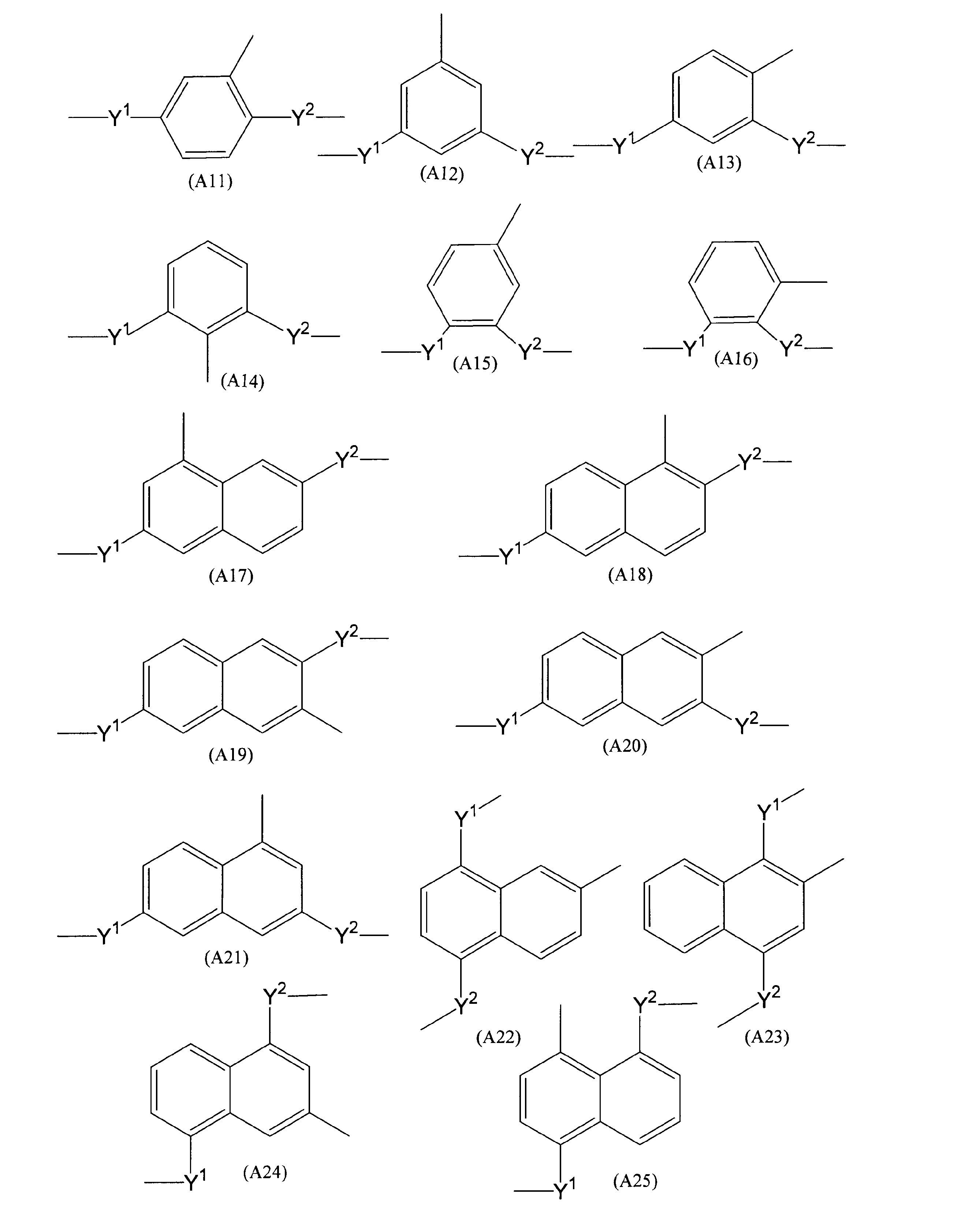
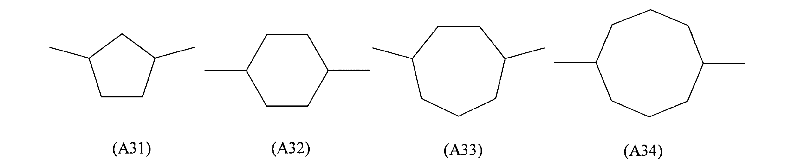
- a 1 groups represented by the following formulas (A11) to (A25) are more preferable.
- A13 groups represented by the following formulas (A11), (A13), (A15), (A19), and (A23) are particularly preferred.
- the divalent aromatic groups of A 4 and A 5 may have a substituent at any position.
- the substituent include a halogen atom, a cyano group, a hydroxyl group, an alkyl group having 1 to 6 carbon atoms, an alkoxy group having 1 to 6 carbon atoms, a nitro group, and a —C ( ⁇ O) —OR 8b group; Can be mentioned.
- R 8b is an alkyl group having 1 to 6 carbon atoms.
- a halogen atom, an alkyl group having 1 to 6 carbon atoms, and an alkoxy group are preferable.
- a compound represented by the formula: D1-J J represents an epoxy group
- a compound represented by the formula: D2-OH in the presence of a base such as sodium hydroxide or potassium hydroxide. Mix and condense.
- a compound represented by the formula: D1-OFN (OFN represents a group having an unsaturated bond) and a compound represented by the formula: D2-OMet, such as sodium hydroxide, potassium hydroxide, etc. In the presence of a base, they are mixed and subjected to an addition reaction.
- a compound represented by the formula: D1-hal and a compound represented by the formula: D2-OMet are mixed and condensed in the presence of copper or cuprous chloride (Ullman condensation).
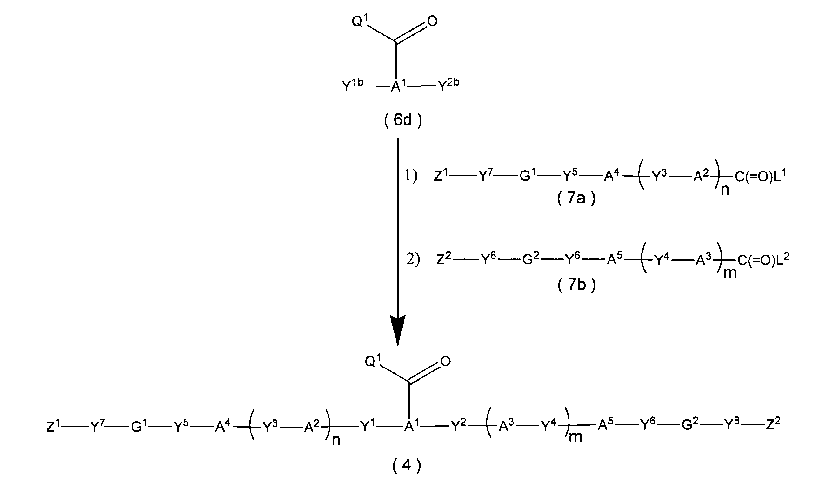
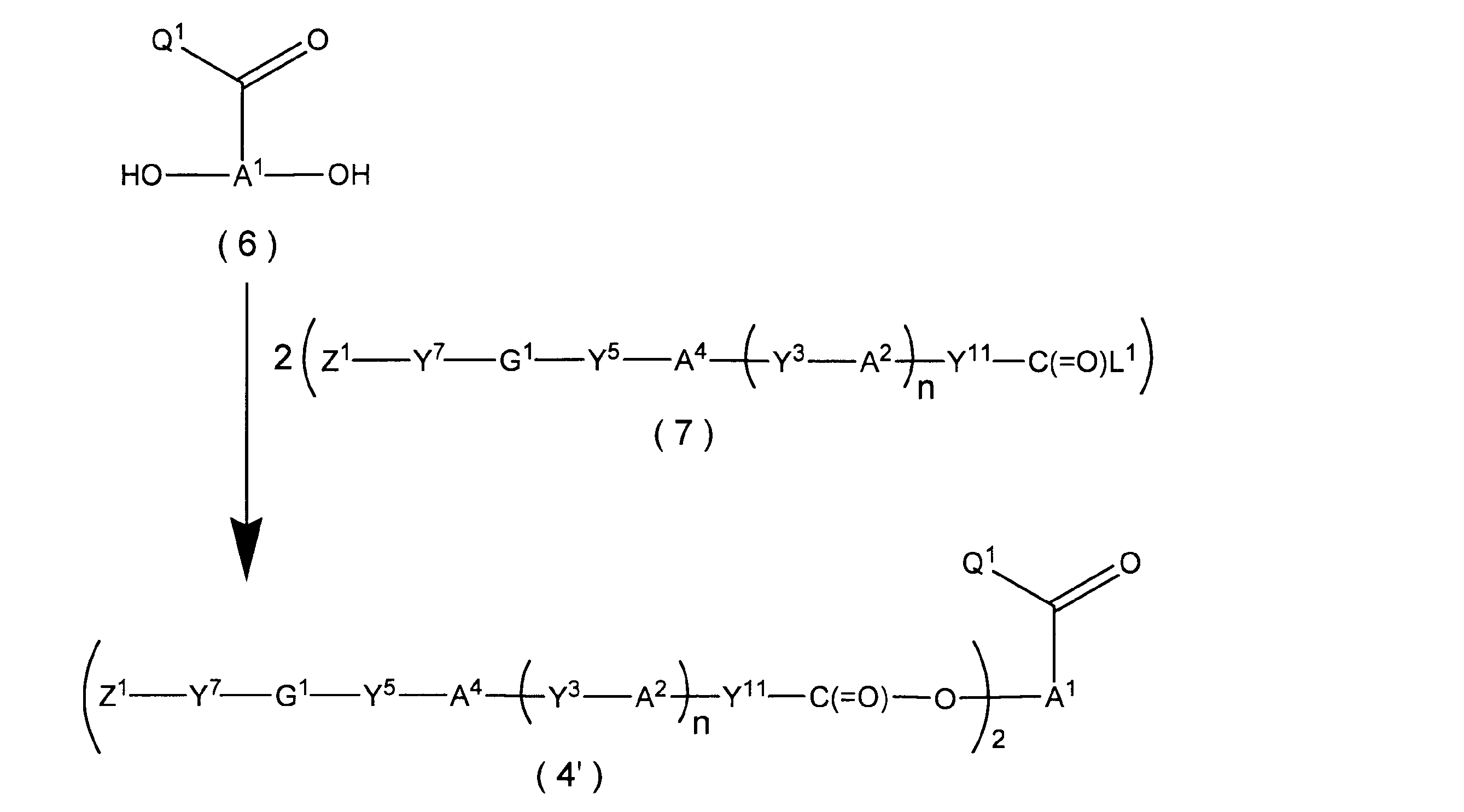
- compound (7) is a compound (carboxylic acid) in which L 1 is a hydroxyl group
- a dehydrating condensing agent such as 1-ethyl-3- (3-dimethylaminopropyl) carbodiimide hydrochloride, dicyclohexylcarbodiimide, etc.
- the target product can be obtained by reacting with.
- the amount of the dehydrating condensing agent to be used is generally 1 mol-3 mol per 1 mol of compound (7).
- the desired product can be obtained by reacting in the presence of a base.
- a base include organic bases such as triethylamine and pyridine; and inorganic bases such as sodium hydroxide, sodium carbonate, and sodium bicarbonate.
- the amount of the base to be used is generally 1 mol-3 mol per 1 mol of compound (7).
Landscapes
- Chemical & Material Sciences (AREA)
- Physics & Mathematics (AREA)
- Crystallography & Structural Chemistry (AREA)
- Nonlinear Science (AREA)
- Engineering & Computer Science (AREA)
- Materials Engineering (AREA)
- Organic Chemistry (AREA)
- General Physics & Mathematics (AREA)
- Optics & Photonics (AREA)
- Mathematical Physics (AREA)
- Polarising Elements (AREA)
- Liquid Crystal Substances (AREA)
Abstract
Description
〔1〕 エチレン性不飽和結合及び芳香環を含有し逆波長分散性の複屈折を発現しうる重合性液晶化合物を含む液晶性組成物の硬化物からなる液晶硬化層を備えた、液晶硬化フィルムであって、
下記式(i):
1.00<X(S)/X(A) (i)
(前記の式(i)において、
X(S)は、前記液晶硬化層の一方の面のピーク比Xを表し、
X(A)は、前記液晶硬化層の他方の面のピーク比Xを表し、
ピーク比Xは、X=I(1)/I(2)で表される比を表し、
I(1)は、赤外全反射吸収スペクトル測定によるエチレン性不飽和結合の面内変角振動由来のピーク強度を表し、
I(2)は、赤外全反射吸収スペクトル測定による芳香環の不飽和結合の伸縮振動由来のピーク強度を表す。)
を満たす、液晶硬化フィルム。
〔2〕 前記液晶硬化層が、逆波長分散性のレターデーションを有する、〔1〕記載の液晶硬化フィルム。
〔3〕 前記液晶性組成物が、界面活性剤を含み、前記液晶硬化層の前記一方の面での前記界面活性剤の量が、前記液晶硬化層の前記他方の面での前記界面活性剤の量よりも、少ない、〔1〕又は〔2〕記載の液晶硬化フィルム。
〔4〕 前記重合性液晶化合物が、前記重合性液晶化合物の分子中に、主鎖メソゲンと、前記主鎖メソゲンに結合した側鎖メソゲンとを含む、〔1〕~〔3〕のいずれか一項に記載の液晶硬化フィルム。
〔5〕 前記重合性液晶化合物が、下記式(I)で表される、〔1〕~〔4〕のいずれか一項に記載の液晶硬化フィルム。
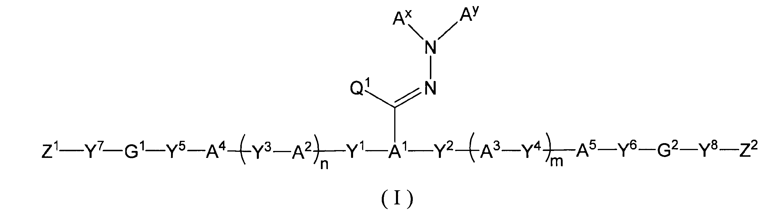
Y1~Y8は、それぞれ独立して、化学的な単結合、-O-、-S-、-O-C(=O)-、-C(=O)-O-、-O-C(=O)-O-、-NR1-C(=O)-、-C(=O)-NR1-、-O-C(=O)-NR1-、-NR1-C(=O)-O-、-NR1-C(=O)-NR1-、-O-NR1-、又は、-NR1-O-を表す。ここで、R1は、水素原子又は炭素数1~6のアルキル基を表す。
G1、G2は、それぞれ独立して、置換基を有していてもよい、炭素数1~20の二価の脂肪族基を表す。また、前記脂肪族基には、1つの脂肪族基当たり1以上の-O-、-S-、-O-C(=O)-、-C(=O)-O-、-O-C(=O)-O-、-NR2-C(=O)-、-C(=O)-NR2-、-NR2-、又は、-C(=O)-が介在していてもよい。ただし、-O-又は-S-がそれぞれ2以上隣接して介在する場合を除く。ここで、R2は、水素原子又は炭素数1~6のアルキル基を表す。
Z1、Z2は、それぞれ独立して、ハロゲン原子で置換されていてもよい炭素数2~10のアルケニル基を表す。
Axは、芳香族炭化水素環及び芳香族複素環からなる群から選ばれる少なくとも一つの芳香環を有する、炭素数2~30の有機基を表す。
Ayは、水素原子、置換基を有していてもよい炭素数1~20のアルキル基、置換基を有していてもよい炭素数2~20のアルケニル基、置換基を有していてもよい炭素数3~12のシクロアルキル基、置換基を有していてもよい炭素数2~20のアルキニル基、-C(=O)-R3、-SO2-R4、-C(=S)NH-R9、又は、芳香族炭化水素環及び芳香族複素環からなる群から選ばれる少なくとも一つの芳香環を有する、炭素数2~30の有機基を表す。ここで、R3は、置換基を有していてもよい炭素数1~20のアルキル基、置換基を有していてもよい炭素数2~20のアルケニル基、置換基を有していてもよい炭素数3~12のシクロアルキル基、又は、炭素数5~12の芳香族炭化水素環基を表す。R4は、炭素数1~20のアルキル基、炭素数2~20のアルケニル基、フェニル基、又は、4-メチルフェニル基を表す。R9は、置換基を有していてもよい炭素数1~20のアルキル基、置換基を有していてもよい炭素数2~20のアルケニル基、置換基を有していてもよい炭素数3~12のシクロアルキル基、又は、置換基を有していてもよい炭素数5~20の芳香族基を表す。前記Ax及びAyが有する芳香環は、置換基を有していてもよい。また、前記AxとAyは、一緒になって、環を形成していてもよい。
A1は、置換基を有していてもよい三価の芳香族基を表す。
A2、A3は、それぞれ独立して、置換基を有していてもよい炭素数3~30の二価の脂環式炭化水素基を表す。
A4、A5は、それぞれ独立して、置換基を有していてもよい、炭素数6~30の二価の芳香族基を表す。
Q1は、水素原子、又は、置換基を有していてもよい炭素数1~6のアルキル基を表す。
m及びnは、それぞれ独立に、0又は1を表す。)
〔6〕 前記重合性液晶化合物が、前記重合性液晶化合物の分子中に、ベンゾチアゾール環、並びに、シクロヘキシル環及びフェニル環の組み合わせ、からなる群より選ばれる少なくとも1種を含有する、〔1〕~〔5〕のいずれか一項に記載の液晶硬化フィルム。
〔7〕 〔1〕~〔6〕のいずれか一項に記載の液晶硬化フィルムの製造方法であって、
基材フィルム上に、前記液晶性組成物の層を形成する工程と、
前記液晶性組成物の層を硬化させて、液晶硬化層を得る工程と、を含む、液晶硬化フィルムの製造方法。
図1は、本発明の一実施形態に係る液晶硬化フィルム100を模式的に示す断面図である。図1に示すように、液晶硬化フィルム100は、逆波長分散性の複屈折を発現しうる重合性液晶化合物を含む液晶性組成物の硬化物からなる液晶硬化層110を備える。以下の説明において、逆波長分散性の複屈折を発現しうる重合性液晶化合物のことを、適宜「逆波長重合性液晶化合物」ということがある。液晶硬化層110において、逆波長重合性液晶化合物としては、その分子構造中にエチレン性不飽和結合及び芳香環を含有する化合物を用いている。
1.00<X(S)/X(A) (i)
(前記の式(i)において、
X(S)は、液晶硬化層110の一方の面(図1では、基材フィルム側の面)110Dのピーク比Xを表し、
X(A)は、液晶硬化層110の他方の面(図1では、空気側の面)110Uのピーク比Xを表し、
ピーク比Xは、X=I(1)/I(2)で表される比を表し、
I(1)は、赤外全反射吸収スペクトル測定によるエチレン性不飽和結合の面内変角振動由来のピーク強度を表し、
I(2)は、赤外全反射吸収スペクトル測定による芳香環の不飽和結合の伸縮振動由来のピーク強度を表す。)
以下の説明において、「赤外全反射吸収スペクトル」のことを、適宜「IRスペクトル」ということがある。
一般に、液晶硬化層を備える液晶硬化フィルムは、液晶硬化層を適切な接着剤を用いて任意の光学部材に貼り合わせて使用されることがある。このような場合、接着剤としては、紫外線硬化型の接着剤を用いることが多い。ところが、従来の液晶硬化フィルムでは、液晶硬化層を接着剤に接触させると、液晶硬化層のレターデーションが変化し、所望の光学特性が得られないことがあった。
液晶硬化フィルム100の測定波長590nmにおける面内レターデーションRe0を測定する。その後、液晶硬化層110の面110Uに、紫外線硬化型の接着剤を厚み100μm以上で塗工して、基材フィルム、液晶硬化層及び接着剤層を備える積層体を得る。液晶硬化層に接着剤を塗工した時点から5分後、前記の積層体の測定波長590nmにおける面内レターデーションRe1を測定する。そして、下記の式(ii)により、接着剤の塗工による面内レターデーションの変化量ΔReを計算する。
ΔRe={(Re0-Re1)/Re0}×100(%) (ii)
こうして得られる面内レターデーションの変化量ΔReの絶対値が小さいほど、液晶硬化層110の接着剤に対する耐性が優れることを示す。
逆波長重合性液晶化合物は、液晶性を有するので、当該逆波長重合性液晶化合物を配向させたときに、液晶相を呈しうる。また、逆波長重合性液晶化合物は、重合性を有するので、前記のように液晶相を呈した状態で重合し、液晶相における分子の配向を維持したまま重合体となりうる。
Δn(450)<Δn(650) (iii)
Δn(450)<Δn(550)<Δn(650) (iv)
また、逆波長重合性液晶化合物の例としては、下記式(Ia)で表される化合物が挙げられる。以下の説明において、式(Ia)で表される化合物を、適宜「化合物(Ia)」ということがある。


R1の炭素数1~6のアルキル基としては、例えば、メチル基、エチル基、n-プロピル基、イソプロピル基、n-ブチル基、sec-ブチル基、t-ブチル基、n-ペンチル基、n-へキシル基が挙げられる。
R1としては、水素原子又は炭素数1~4のアルキル基が好ましい。
炭素数1~20の二価の脂肪族基としては、例えば、炭素数1~20のアルキレン基、炭素数2~20のアルケニレン基等の鎖状構造を有する二価の脂肪族基;炭素数3~20のシクロアルカンジイル基、炭素数4~20のシクロアルケンジイル基、炭素数10~30の二価の脂環式縮合環基等の二価の脂肪族基;が挙げられる。
前記脂肪族基に介在する基としては、-O-、-O-C(=O)-、-C(=O)-O-、-C(=O)-が好ましい。
該アルケニル基の炭素数としては、2~6が好ましい。Z1及びZ2のアルケニル基の置換基であるハロゲン原子としては、フッ素原子、塩素原子、臭素原子等が挙げられ、塩素原子が好ましい。
さらに、Axの炭素数2~30の有機基の「炭素数」は、置換基の炭素原子を含まない有機基全体の総炭素数を意味する(後述するAyにて同じである。)。
(1)芳香族炭化水素環基

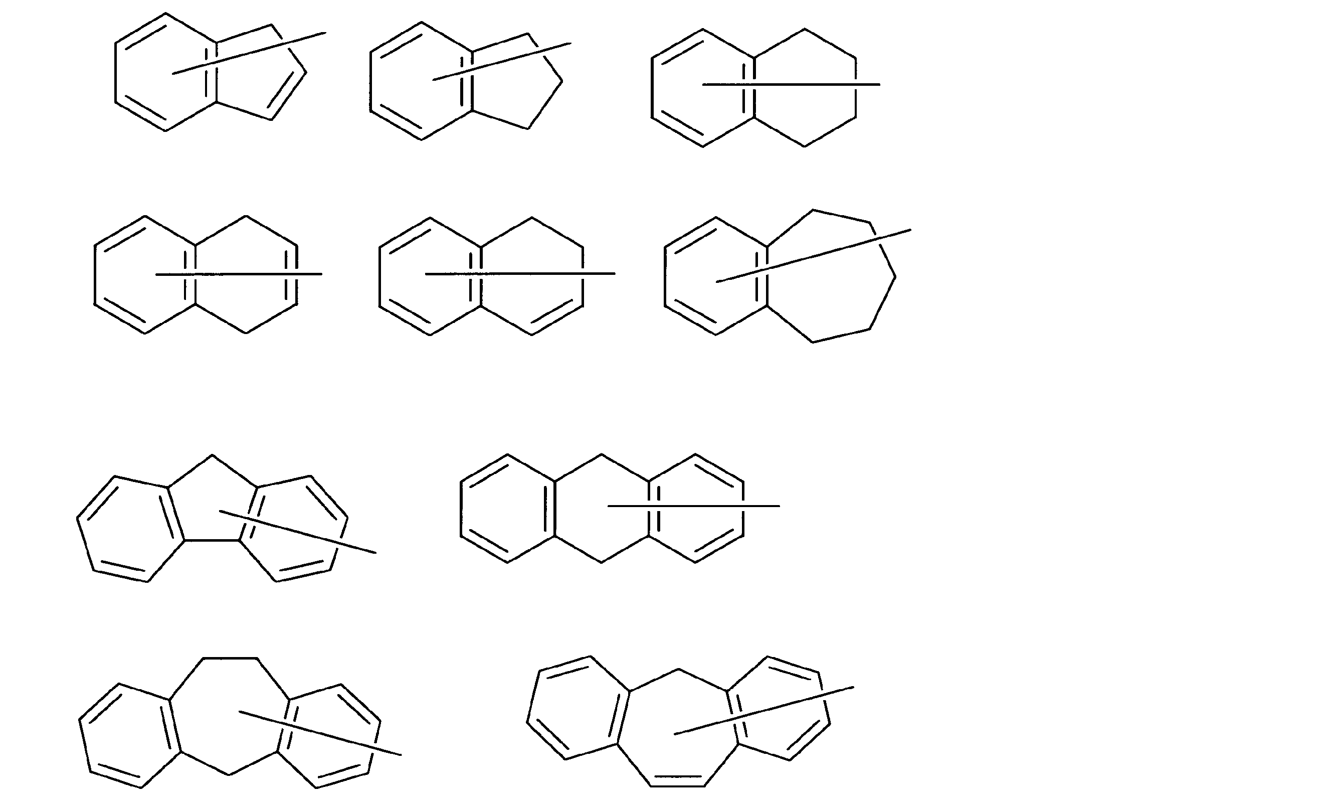
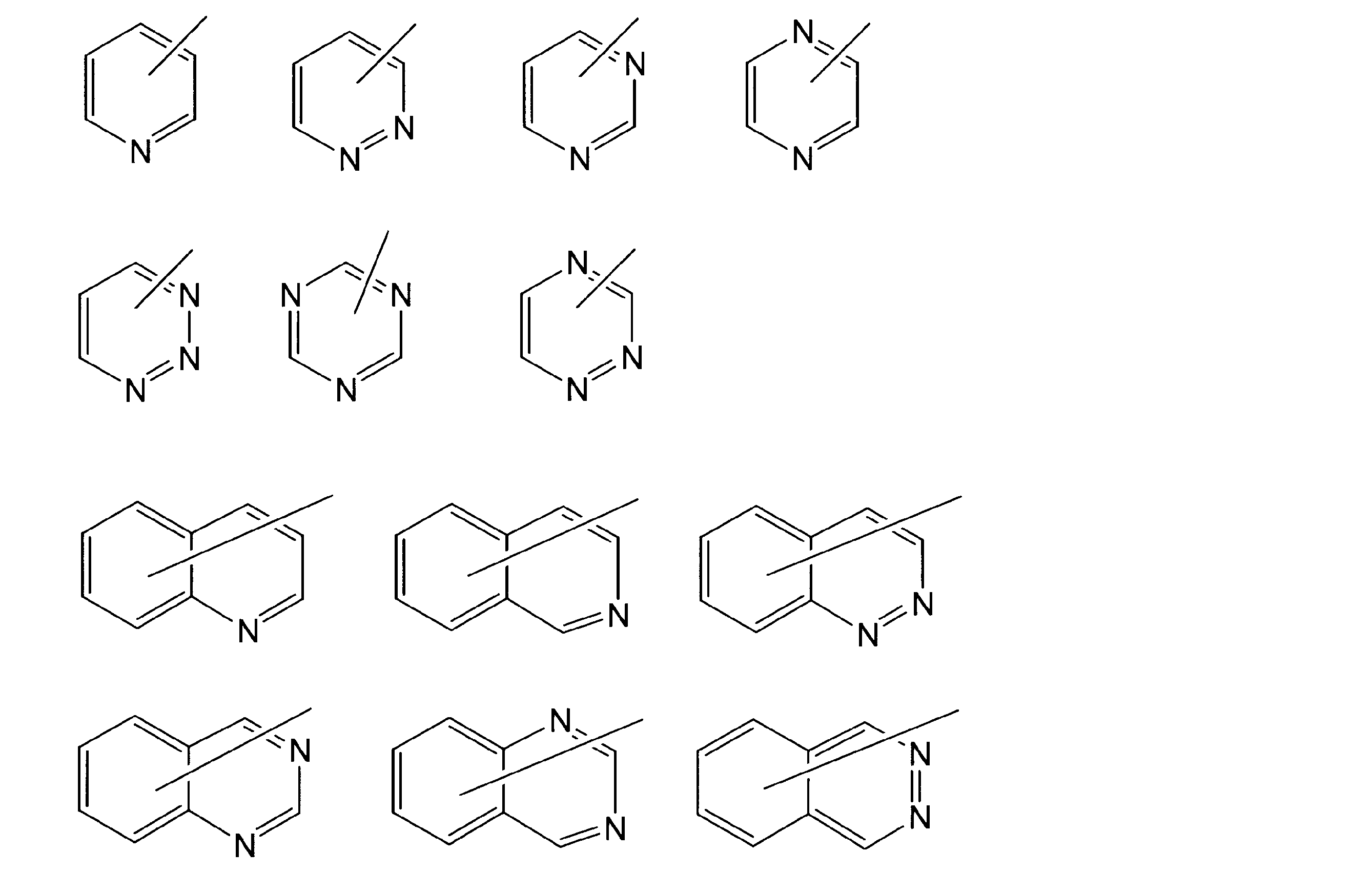


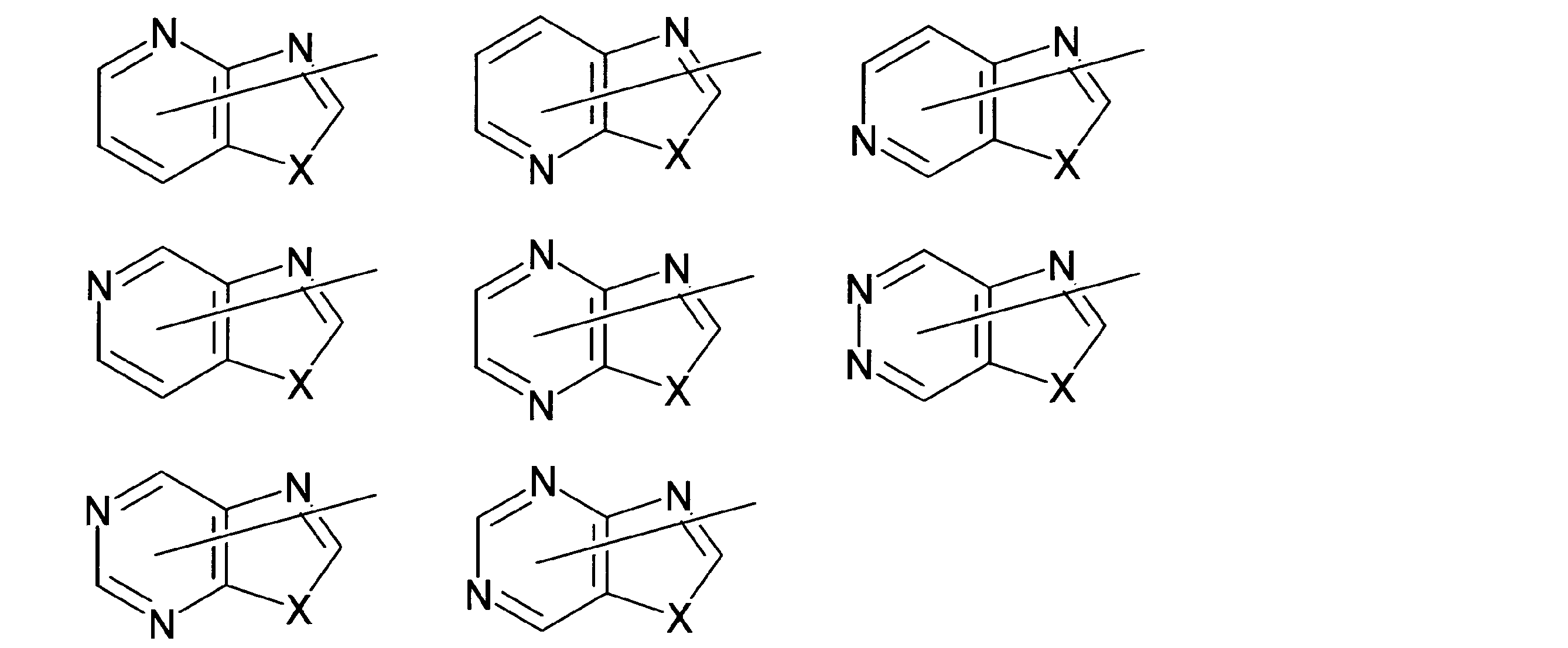

(3)芳香族炭化水素環及び複素環の組み合わせを含む基
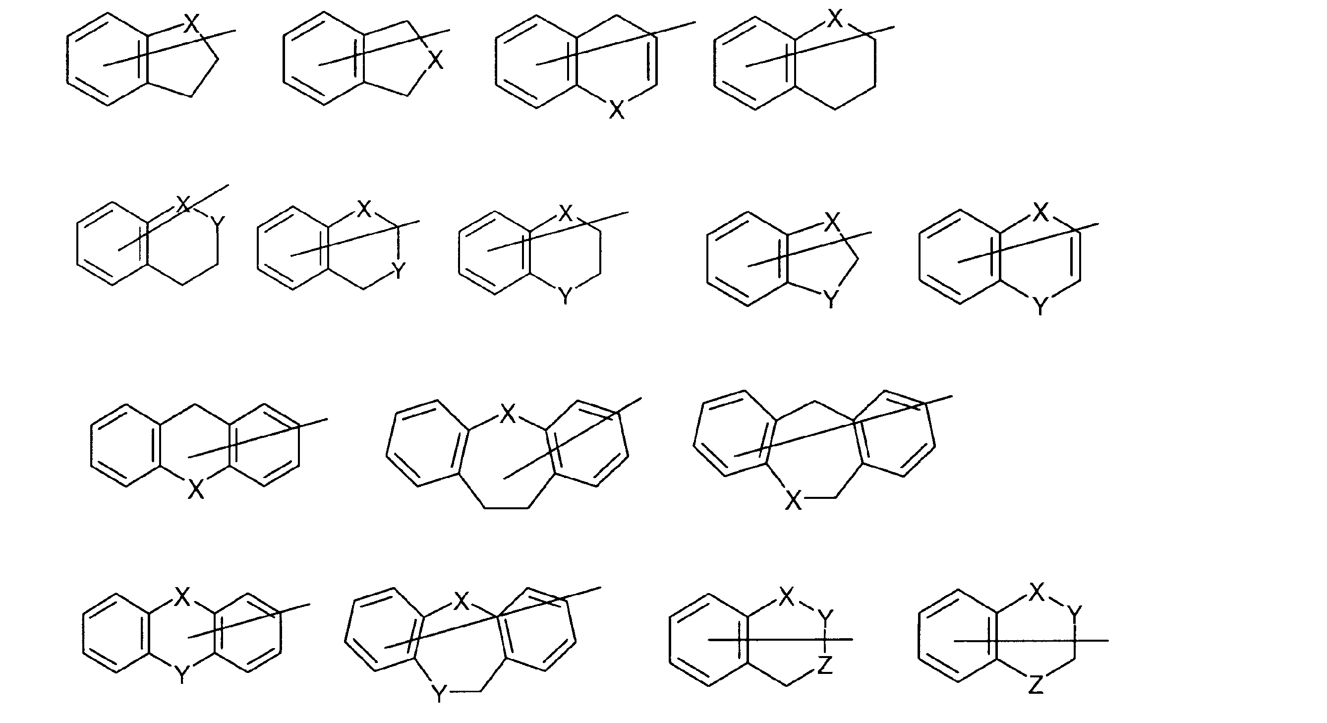
(4)芳香族炭化水素環及び芳香族複素環からなる群から選ばれる少なくとも一つの芳香環を有する、アルキル基




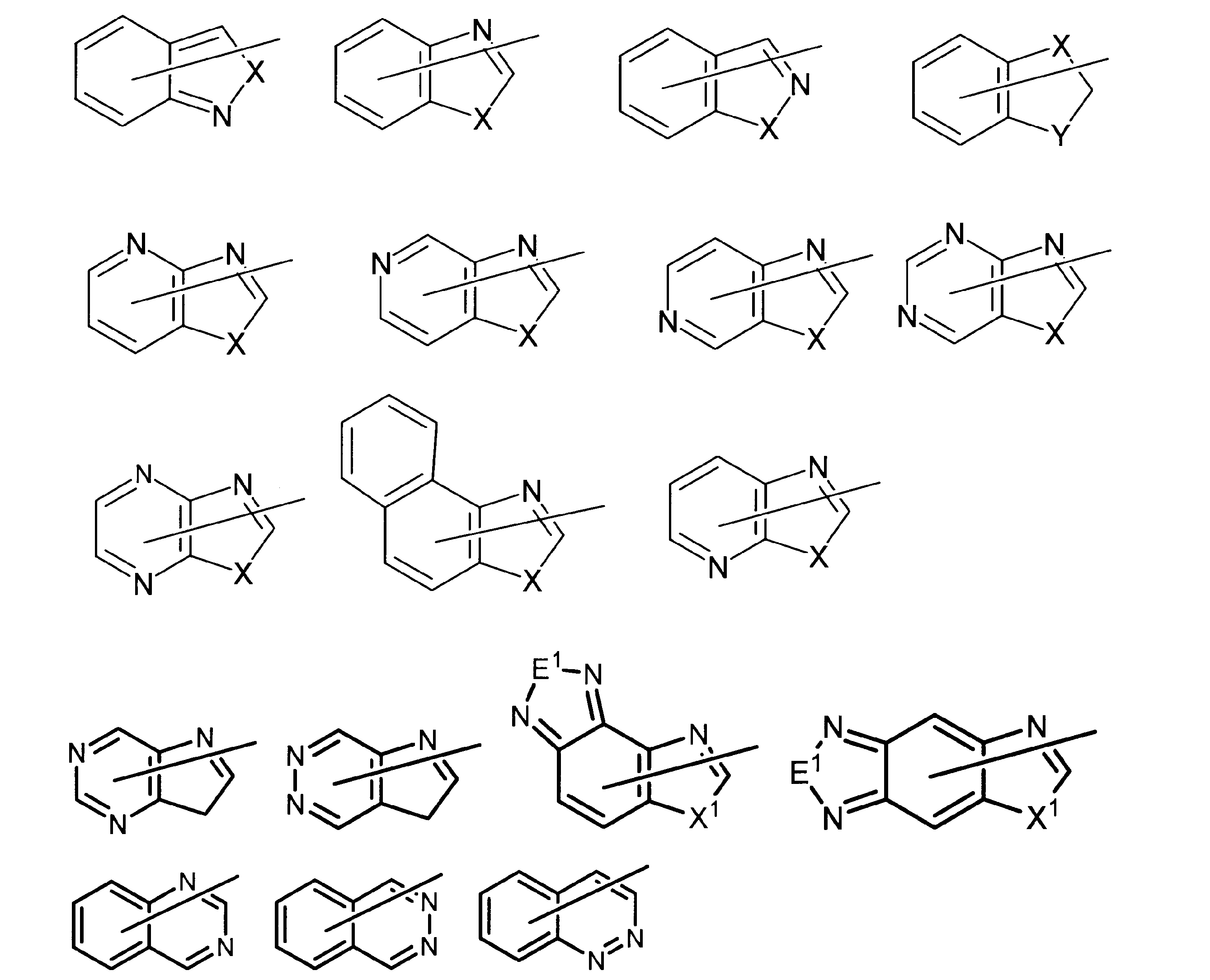

Axの炭素数2~30の有機基の「炭素数」は、置換基の炭素原子を含まない有機基全体の総炭素数を意味する(後述するAyにて同じである。)。
AxとAyが一緒になって形成される環としては、例えば、下記に示す環が挙げられる。なお、下記に示す環は、式(I)中の



また、これらの環は置換基を有していてもよい。かかる置換基としては、Axが有する芳香環の置換基として説明したのと同様のものが挙げられる。
(α)Axが炭素数4~30の、芳香族炭化水素環基、芳香族複素環基、又は、芳香族炭化水素環及び複素環の組み合わせを含む基であり、Ayが水素原子、炭素数3~8のシクロアルキル基、(ハロゲン原子、シアノ基、炭素数1~6のアルキル基、炭素数1~6のアルコキシ基、若しくは炭素数3~8のシクロアルキル基)を置換基として有していてもよい炭素数6~12の芳香族炭化水素環基、(ハロゲン原子、炭素数1~6のアルキル基、炭素数1~6のアルコキシ基、シアノ基)を置換基として有していてもよい炭素数3~9の芳香族複素環基、(ハロゲン原子、炭素数1~6のアルキル基、炭素数1~6のアルコキシ基、シアノ基)を置換基として有していてもよく芳香族炭化水素環及び複素環の組み合わせを含む炭素数3~9の基、置換基を有していてもよい炭素数1~20のアルキル基、置換基を有していてもよい炭素数1~20のアルケニル基、又は、置換基を有していてもよい炭素数2~20のアルキニル基であり、当該置換基が、ハロゲン原子、シアノ基、炭素数1~20のアルコキシ基、炭素数1~12のアルコキシ基で置換された炭素数1~12のアルコキシ基、フェニル基、シクロヘキシル基、炭素数2~12の環状エーテル基、炭素数6~14のアリールオキシ基、水酸基、ベンゾジオキサニル基、ベンゼンスルホニル基、ベンゾイル基及び-SR10のいずれかである組み合わせ。
(β)AxとAyが一緒になって不飽和複素環又は不飽和炭素環を形成している組み合わせ。
ここで、R10は前記と同じ意味を表す。
(γ)Axが下記構造を有する基のいずれかであり、Ayが水素原子、炭素数3~8のシクロアルキル基、(ハロゲン原子、シアノ基、炭素数1~6のアルキル基、炭素数1~6のアルコキシ基、若しくは炭素数3~8のシクロアルキル基)を置換基として有していてもよい炭素数6~12の芳香族炭化水素環基、(ハロゲン原子、炭素数1~6のアルキル基、炭素数1~6のアルコキシ基、シアノ基)を置換基として有していてもよい炭素数3~9の芳香族複素環基、(ハロゲン原子、炭素数1~6のアルキル基、炭素数1~6のアルコキシ基、シアノ基)を置換基として有していてもよく芳香族炭化水素環及び複素環の組み合わせを含む炭素数3~9の基、置換基を有していてもよい炭素数1~20のアルキル基、置換基を有していてもよい炭素数1~20のアルケニル基、又は、置換基を有していてもよい炭素数2~20のアルキニル基であり、当該置換基が、ハロゲン原子、シアノ基、炭素数1~20のアルコキシ基、炭素数1~12のアルコキシ基で置換された炭素数1~12のアルコキシ基、フェニル基、シクロヘキシル基、炭素数2~12の環状エーテル基、炭素数6~14のアリールオキシ基、水酸基、ベンゾジオキサニル基、ベンゼンスルホニル基、ベンゾイル基、-SR10のいずれかである組み合わせ。
ここで、R10は前記と同じ意味を表す。


AxとAyの特に好ましい組み合わせとしては、下記の組み合わせ(δ)が挙げられる。
(δ)Axが下記構造を有する基のいずれかであり、Ayが水素原子、炭素数3~8のシクロアルキル基、(ハロゲン原子、シアノ基、炭素数1~6のアルキル基、炭素数1~6のアルコキシ基、若しくは炭素数3~8のシクロアルキル基)を置換基として有していてもよい炭素数6~12の芳香族炭化水素環基、(ハロゲン原子、炭素数1~6のアルキル基、炭素数1~6のアルコキシ基、シアノ基)を置換基として有していてもよい炭素数3~9の芳香族複素環基、(ハロゲン原子、炭素数1~6のアルキル基、炭素数1~6のアルコキシ基、シアノ基)を置換基として有していてもよく芳香族炭化水素環及び複素環の組み合わせを含む炭素数3~9の基、置換基を有していてもよい炭素数1~20のアルキル基、置換基を有していてもよい炭素数1~20のアルケニル基、又は、置換基を有していてもよい炭素数2~20のアルキニル基であり、当該置換基が、ハロゲン原子、シアノ基、炭素数1~20のアルコキシ基、炭素数1~12のアルコキシ基で置換された炭素数1~12のアルコキシ基、フェニル基、シクロヘキシル基、炭素数2~12の環状エーテル基、炭素数6~14のアリールオキシ基、水酸基、ベンゾジオキサニル基、ベンゼンスルホニル基、ベンゾイル基、及び、-SR10のいずれかである組み合わせ。
下記式中、Xは前記と同じ意味を表す。ここで、R10は前記と同じ意味を表す。
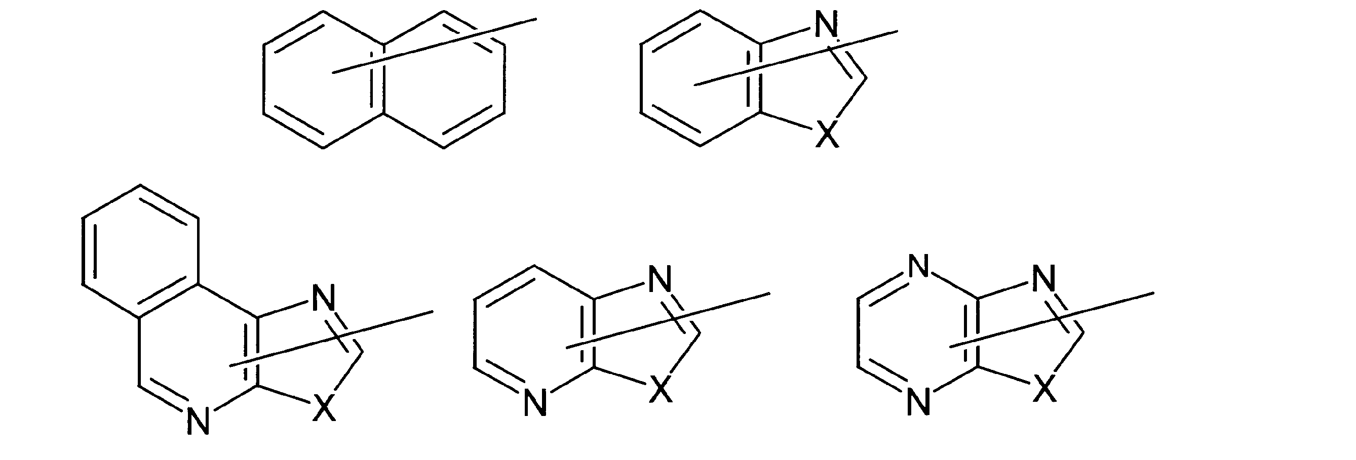
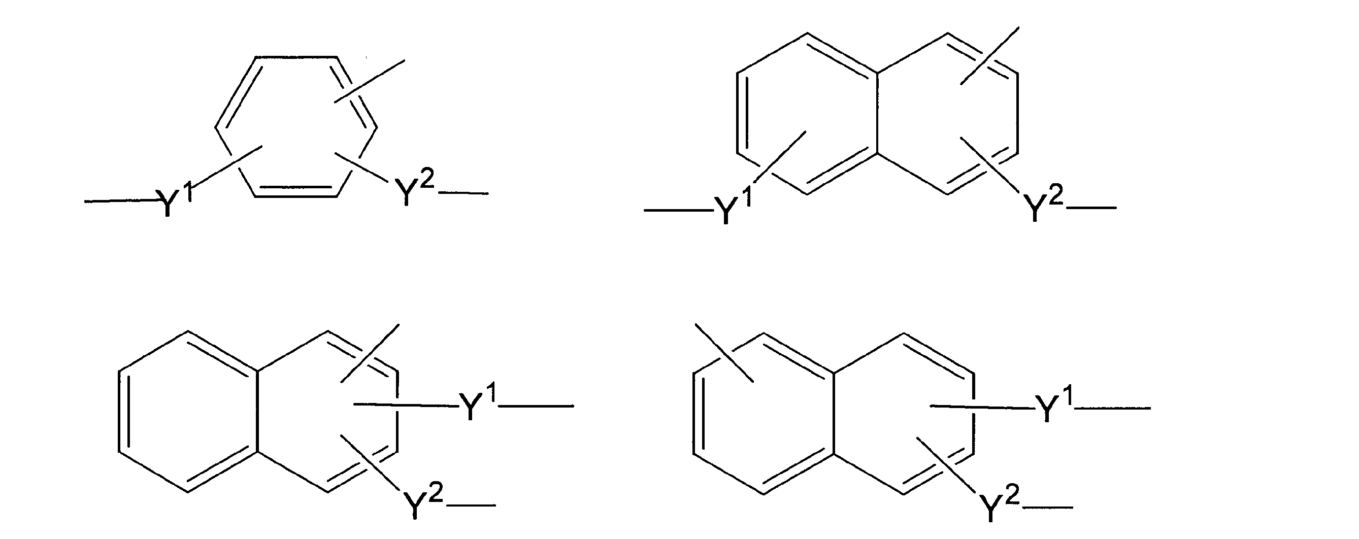


また、ジアゾニウム塩(5)は、アニリン等の化合物から常法により製造しうる。
(i)式:D1-hal(halはハロゲン原子を表す。以下にて同じ。)で表される化合物と、式:D2-OMet(Metはアルカリ金属(主にナトリウム)を表す。以下にて同じ。)で表される化合物とを、混合して縮合させる(ウイリアムソン合成)。なお、式中、D1及びD2は任意の有機基を表す(以下にて同じ。)。
(ii)式:D1-halで表される化合物と、式:D2-OHで表される化合物とを、水酸化ナトリウム、水酸化カリウム等の塩基存在下、混合して縮合させる。
(iii)式:D1-J(Jはエポキシ基を表す。)で表される化合物と、式:D2-OHで表される化合物とを、水酸化ナトリウム、水酸化カリウム等の塩基存在下、混合して縮合させる。
(iv)式:D1-OFN(OFNは不飽和結合を有する基を表す。)で表される化合物と、式:D2-OMetで表される化合物とを、水酸化ナトリウム、水酸化カリウム等の塩基存在下、混合して付加反応させる。
(v)式:D1-halで表される化合物と、式:D2-OMetで表される化合物とを、銅あるいは塩化第一銅の存在下、混合して縮合させる(ウルマン縮合)。
(vi)式:D1-COOHで表される化合物と、式:D2-OH又はD2-NH2で表される化合物とを、脱水縮合剤(N,N-ジシクロヘキシルカルボジイミド等)の存在下に脱水縮合させる。
(vii)式:D1-COOHで表される化合物にハロゲン化剤を作用させることにより、式:D1-CO-halで表される化合物を得て、このものと式:D2-OH又はD2-NH2で表される化合物とを、塩基の存在下に反応させる。
(viii)式:D1-COOHで表される化合物に酸無水物を作用させることにより、混合酸無水物を得た後、このものと式:D2-OH又はD2-NH2で表される化合物とを反応させる。
(ix)式:D1-COOHで表される化合物と、式:D2-OH又はD2-NH2で表される化合物とを、酸触媒あるいは塩基触媒の存在下に脱水縮合させる。
溶媒の使用量は、特に限定されず、用いる化合物の種類及び反応規模等を考慮して設定しうる。溶媒の具体的な使用量は、ヒドロキシ化合物(6)1gに対し、通常1g~50gである。

また、化合物(6)として、市販されているものをそのまま、又は所望により精製して用いてもよい。

スルホニルクロライドの使用量は、化合物(9’)1当量に対して、通常0.5当量~0.7当量である。
また、化合物(8)の使用量は、化合物(9’)1当量に対して、通常0.5当量~0.6当量である。
塩基の使用量は、化合物(9’)1当量に対して、通常0.5当量~0.7当量である。
反応温度は、20℃~30℃であり、反応時間は反応規模等にもよるが、数分から数時間である。
溶媒の使用量は、特に限定されず、用いる化合物の種類及び反応規模等を考慮して設定しうる。溶媒の具体的な使用量は、化合物(9’)1gに対し、通常1g~50gである。
目的とする化合物の構造は、NMRスペクトル、IRスペクトル、マススペクトル等の測定、元素分析等により、同定できる。

液晶性組成物は、上述した逆波長重合性液晶化合物を含む。また、液晶性組成物は、逆波長重合性液晶化合物に組み合わせて、任意の成分を含みうる。これらの任意の成分は、1種類を単独で用いてもよく、2種類以上を任意の比率で組み合わせて用いてもよい。
液晶硬化層は、上述した液晶性組成物の硬化物からなる層である。この液晶硬化層は、当該液晶硬化層の厚み方向に対して垂直な2つの面(おもて面及び裏面)のピーク比Xが、式(i)を満たす。より詳しくは、X(S)/X(A)は、通常1.00より大きく、好ましくは1.05より大きく、また、好ましくは1.30未満、より好ましくは1.25未満である。X(S)/X(A)が、前記範囲の下限値より大きいことにより、液晶硬化層の耐傷付き性を良好にでき、更に通常は、液晶硬化層の接着剤耐性及び剥離性を良好にできる。また、X(S)/X(A)が、前記範囲の上限値未満であることにより、液晶硬化層の経年変化などによる耐久性の低下を抑制できる。
液晶硬化フィルムの液晶硬化層の面のIRスペクトルを測定する。測定したIRスペクトルから、エチレン性不飽和結合の面内変角振動に由来する1407.7809cm-1のピーク強度I(1)、及び、芳香環の不飽和結合の伸縮振動に由来する1505.1685cm-1のピーク強度I(2)を求める。これらのピーク強度I(1)及びI(2)から、液晶硬化層の各面のピーク比X(S)及びX(A)を計算する。
Re(450)<Re(650) (v)
Re(450)<Re(550)<Re(650) (vi)
液晶硬化フィルムは、液晶硬化層の形成に用いた基材フィルムを備えていてもよい。このような基材フィルムとして、通常は、樹脂フィルムを用いる。樹脂としては、各種の重合体を含む樹脂が挙げられる。当該重合体としては、例えば、ノルボルネン系重合体等の脂環式構造含有重合体、セルロースエステル、ポリビニルアルコール、ポリイミド、UV透過アクリル、ポリカーボネート、ポリスルホン、ポリエーテルスルホン、エポキシ重合体、ポリスチレン、及び、これらの組み合わせが挙げられる。これらの中でも、透明性、低吸湿性、寸法安定性及び軽量性の観点から、脂環式構造含有重合体及びセルロースエステルが好ましく、脂環式構造含有重合体がより好ましい。
前記の延伸は、テンター延伸機などの延伸機を用いて行いうる。
液晶硬化フィルムは、上述した液晶硬化層に、基材フィルム以外の任意の層を備えていてもよい。例えば、液晶硬化フィルムは、液晶硬化層の基材フィルムとは反対側の面に、任意の層を備えていてもよい。任意の層の例としては、他の部材と接着するための接着剤層、フィルムの滑り性を良くするマット層、耐衝撃性ポリメタクリレート樹脂層などのハードコート層、反射防止層、防汚層等が挙げられる。
液晶硬化フィルムは、その用途に応じた適切な特性を有することが好ましい。例えば、液晶硬化フィルムを光学フィルムとして用いる場合、液晶硬化層が有しうるレターデーションReの範囲として説明したのと同様の範囲のレターデーションを有しうる。
上述した液晶硬化フィルムは、基材フィルム上に液晶性組成物の層を形成する工程と、液晶性組成物の層を硬化させて液晶硬化層を得る工程と、を含む製造方法によって、製造できる。
液晶硬化フィルムの製造方法は、例えば、逆波長重合性液晶化合物を重合させる工程の前に、液晶性組成物の層を乾燥させる工程を含んでいてもよい。かかる乾燥は、自然乾燥、加熱乾燥、減圧乾燥、減圧加熱乾燥等の乾燥方法で達成しうる。かかる乾燥により、液晶性組成物の層から、溶媒を除去することができる。
また、液晶硬化フィルムの製造方法は、例えば、製造された液晶硬化フィルムから基材フィルムを剥離する工程を含んでいてもよい。
さらに、液晶硬化フィルムの製造方法は、例えば、製造された液晶硬化フィルムに、更に任意の層を設ける工程を含んでいてもよい。
液晶硬化フィルムの用途は、任意である。好ましくは、液晶硬化フィルムは、光学フィルムとして用いうる。
〔1.IRスペクトルの測定方法〕
液晶硬化フィルムの液晶硬化層の空気側の面と、樹脂フィルム(日本ゼオン社製「ゼオノアフィルム」)とを、粘着剤を用いて貼り合わせた。その後、基材フィルムを剥離して、液晶硬化層の基材フィルム側の面を露出させた。こうして得られた樹脂フィルム及び液晶硬化層を備える試料を用いて、液晶硬化層の基材フィルム側の面のIRスペクトルを測定した。
液晶硬化フィルムのヘイズを、ヘイズメーター(東洋精機社製「HAZE-GARD II」)を用いて測定した。
擦り試験後のヘイズから擦り試験前のヘイズの値を引き算して、ヘイズの変化量Δhaze(%)を求めた。
分子内に水酸基を含む(メタ)アクリレートモノマーである「2-ヒドロキシ-3-アクリロイロキシプロピルメタクリレート」を7部、水酸基を含まないアクリレートモノマーである「3-メチル-1,5-ペンタンジオールジアクリレート」を90部、及び光重合開始剤(BASF社製「Irgacure2959」)を3部仕込み、十分に撹拌を行い、十分に脱泡を行った。これにより、紫外線硬化型の接着剤を得た。
その後、液晶硬化フィルムの液晶硬化層の空気側の面に、前記の紫外線硬化型の接着剤を厚み100μm以上で塗工して、基材フィルム、液晶硬化層及び接着剤層を備える積層体を得た。
液晶硬化層に接着剤を塗工した時点から5分後、前記の積層体の測定波長590nmにおける面内レターデーションRe1を、前記の位相差計を用いて測定した。
ΔRe={(Re0-Re1)/Re0}×100(%) (ii)
面内レターデーションの変化量ΔReの絶対値が小さいほど、液晶硬化層の接着剤に対する耐性が優れることを示す。
液晶硬化フィルムを2cm×5cmの大きさで切り出してサンプルを得て、このサンプルの液晶硬化層の空気側の面と、樹脂フィルム(日本ゼオン社製「ゼオノアフィルム」)とを、粘着剤を用いて貼り合わせた。その後、基材フィルムを剥離し、剥離した基材フィルムを観察した。
剥離した基材フィルムの全体にわたって、基材フィルムに液晶硬化層が付着していなければ、転写性を「良」と判定した。また、剥離した基材フィルムに液晶硬化層の一部が付着していれば、転写性を「不良」と判定した。
実施例及び比較例で用いた液晶化合物を、溶媒である1,3-ジオキソランに溶解し、様々な濃度の検量線作成用の溶液を得た。これらの溶液を汎用HPLC(島津製作所社製「Prominence」)で分析し、検量線を作成した。
溶媒:アセトニトリル
流速:1mL/min
使用カラム: Eclipse XDB-C18(Agilent社製)
液晶硬化層の空気側の面におけるフッ素の含有率(%:原子数の百分率)f1を、液晶硬化フィルム自体を試料として用いて、下記の条件に従ってX線光電子分光法により、測定した。
励起X線:Al Kα線
フィラメントEmission:10mA
AnodeHT:15kV
中和銃:Electron Neutralizer
中和条件 Filament Current:1.55A
Charge Balance:3.3V
Filament Bias:1.5V
分析エリア:約700μm×300μm
光電子検出角度:0°(試料面と検出器のなす角度:90°)
熱可塑性ノルボルネン樹脂のペレット(日本ゼオン社製「ZEONOR1420R」)を90℃で5時間乾燥させた。乾燥させたペレットを押し出し機に供給し、押し出し機内で溶融させ、ポリマーパイプ及びポリマーフィルターを通し、Tダイからキャスティングドラム上にフィルム状に押し出し、冷却して、厚み60μm、幅1490mmの長尺の延伸前基材を製造した。この製造した延伸前基材を巻き取って、ロールを得た。
(1.1.液晶性組成物の製造)
下記式(E1)で示す構造を有する逆波長重合性液晶化合物(E1)100重量部、界面活性剤(DIC社製「F562」)0.3重量部、及び、光重合開始剤(BASF社製「IRGACURE379EG」)3重量部を、溶媒であるシクロペンタノン146.5重量部及び1,3-ジオキソラン219.8重量部と混合して、完全に溶解させた。こうして得られた混合液を、孔径0.45μmのディスクフィルターで濾過して、液状の液晶性組成物を製造した。

前記の液晶性組成物を、製造例1で製造した基材フィルム上に、ワイヤーバー(#6)を用いて塗工して、液晶性組成物の層を形成した。液晶性組成物の層を、オーブン(ヤマト科学社製「イナートオーブンDN410I」)を用いて、液晶化合物の液晶化温度以上の温度である110℃で、4分間加熱し、乾燥処理及び配向処理を行った。
こうして得られた液晶硬化フィルムを、上述した方法によって評価した。
光重合開始剤の種類をBASF社製「IRGACURE907」に変更した。以上の事項以外は、実施例1と同様にして、液晶硬化フィルムの製造及び評価を行った。形成された液晶硬化層には、逆波長重合性液晶化合物(E1)を重合させた重合体が、ホモジニアス配向規則性を有して含まれていた。また、液晶硬化層の遅相軸の角度は、塗工に用いた基材フィルムの遅相軸と同じく、巻取方向に対して45°の角度をなしていることが確認された。
光重合開始剤の種類をBASF社製「LucirinTPO」に変更した。以上の事項以外は、実施例1と同様にして、液晶硬化フィルムの製造及び評価を行った。形成された液晶硬化層には、逆波長重合性液晶化合物(E1)を重合させた重合体が、ホモジニアス配向規則性を有して含まれていた。また、液晶硬化層の遅相軸の角度は、塗工に用いた基材フィルムの遅相軸と同じく、巻取方向に対して45°の角度をなしていることが確認された。
逆波長重合性液晶化合物(E1)100部の代わりに、逆波長重合性液晶化合物(E1)80部と、下記式(F1)で示す構造を有する順波長重合性液晶化合物(BASF社製「LC242」)20部とを組み合わせて用いた。以上の事項以外は、実施例1と同様にして、液晶硬化フィルムの製造及び評価を行った。形成された液晶硬化層には、逆波長重合性液晶化合物(E1)及び下記式(F1)で示す構造を有する順波長重合性液晶化合物を重合させた重合体が、ホモジニアス配向規則性を有して含まれていた。また、液晶硬化層の遅相軸の角度は、塗工に用いた基材フィルムの遅相軸と同じく、巻取方向に対して45°の角度をなしていることが確認された。

逆波長重合性液晶化合物(E1)100部の代わりに、逆波長重合性液晶化合物(E1)60部と、前記式(F1)で示す構造を有する順波長重合性液晶化合物(BASF社製「LC242」)40部とを組み合わせて用いた。以上の事項以外は、実施例1と同様にして、液晶硬化フィルムの製造及び評価を行った。形成された液晶硬化層には、逆波長重合性液晶化合物(E1)及び前記式(F1)で示す構造を有する順波長重合性液晶化合物を重合させた重合体が、ホモジニアス配向規則性を有して含まれていた。また、液晶硬化層の遅相軸の角度は、塗工に用いた基材フィルムの遅相軸と同じく、巻取方向に対して45°の角度をなしていることが確認された。
逆波長重合性液晶化合物(E1)100部の代わりに、逆波長重合性液晶化合物(E1)80部と、下記式(F2)で示す構造を有する順波長重合性液晶化合物(BASF社製「LC1057」)20部とを組み合わせて用いた。以上の事項以外は、実施例1と同様にして、液晶硬化フィルムの製造及び評価を行った。形成された液晶硬化層には、逆波長重合性液晶化合物(E1)及び下記式(F2)で示す構造を有する順波長重合性液晶化合物を重合させた重合体が、ホモジニアス配向規則性を有して含まれていた。また、液晶硬化層の遅相軸の角度は、塗工に用いた基材フィルムの遅相軸と同じく、巻取方向に対して45°の角度をなしていることが確認された。

逆波長重合性液晶化合物(E1)100部の代わりに、逆波長重合性液晶化合物(E1)60部と、前記式(F2)で示す構造を有する順波長重合性液晶化合物(BASF社製「LC1057」)40部とを組み合わせて用いた。以上の事項以外は、実施例1と同様にして、液晶硬化フィルムの製造及び評価を行った。形成された液晶硬化層には、逆波長重合性液晶化合物(E1)及び前記式(F2)で示す構造を有する順波長重合性液晶化合物を重合させた重合体が、ホモジニアス配向規則性を有して含まれていた。また、液晶硬化層の遅相軸の角度は、塗工に用いた基材フィルムの遅相軸と同じく、巻取方向に対して45°の角度をなしていることが確認された。
液晶性組成物の層への紫外線の照射を、液晶性組成物の層の空気側の面にではなく、基材フィルムを通して行った。以上の事項以外は、実施例1と同様にして、液晶硬化フィルムの製造及び評価を行った。
上述した実施例及び比較例の構成を表1に示し、その結果を表2に示す。
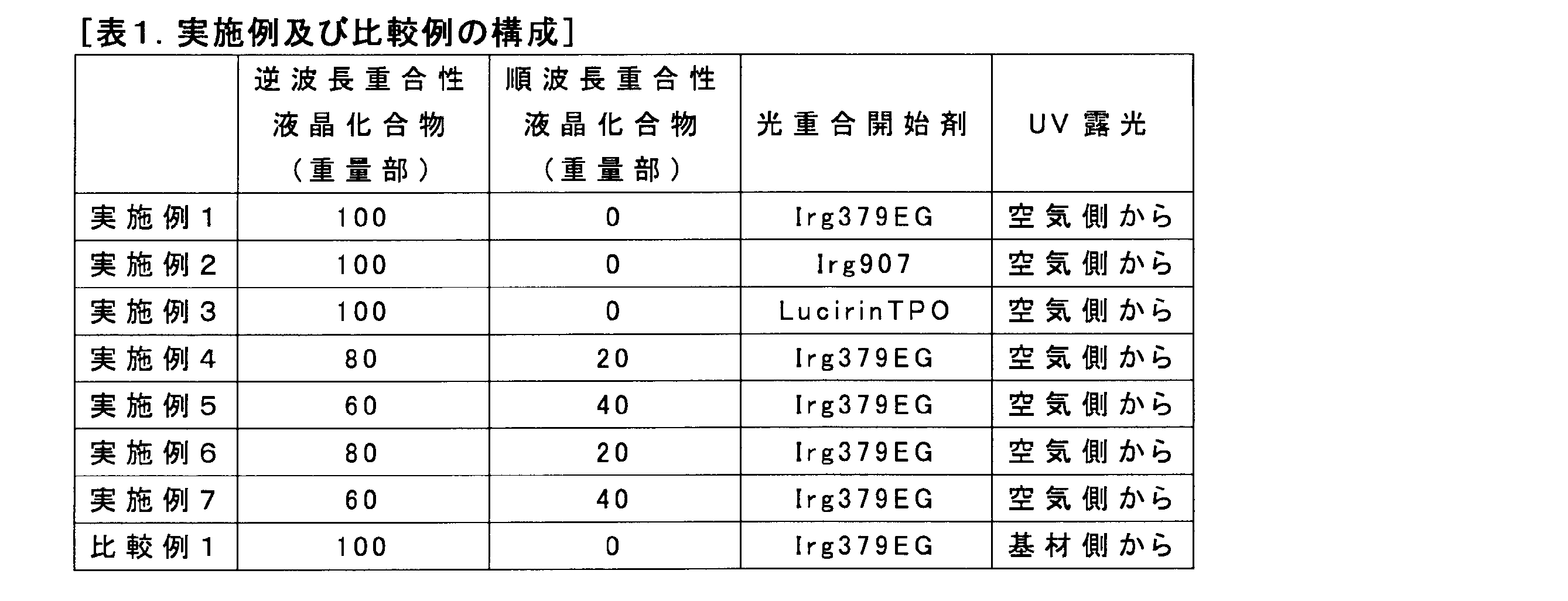
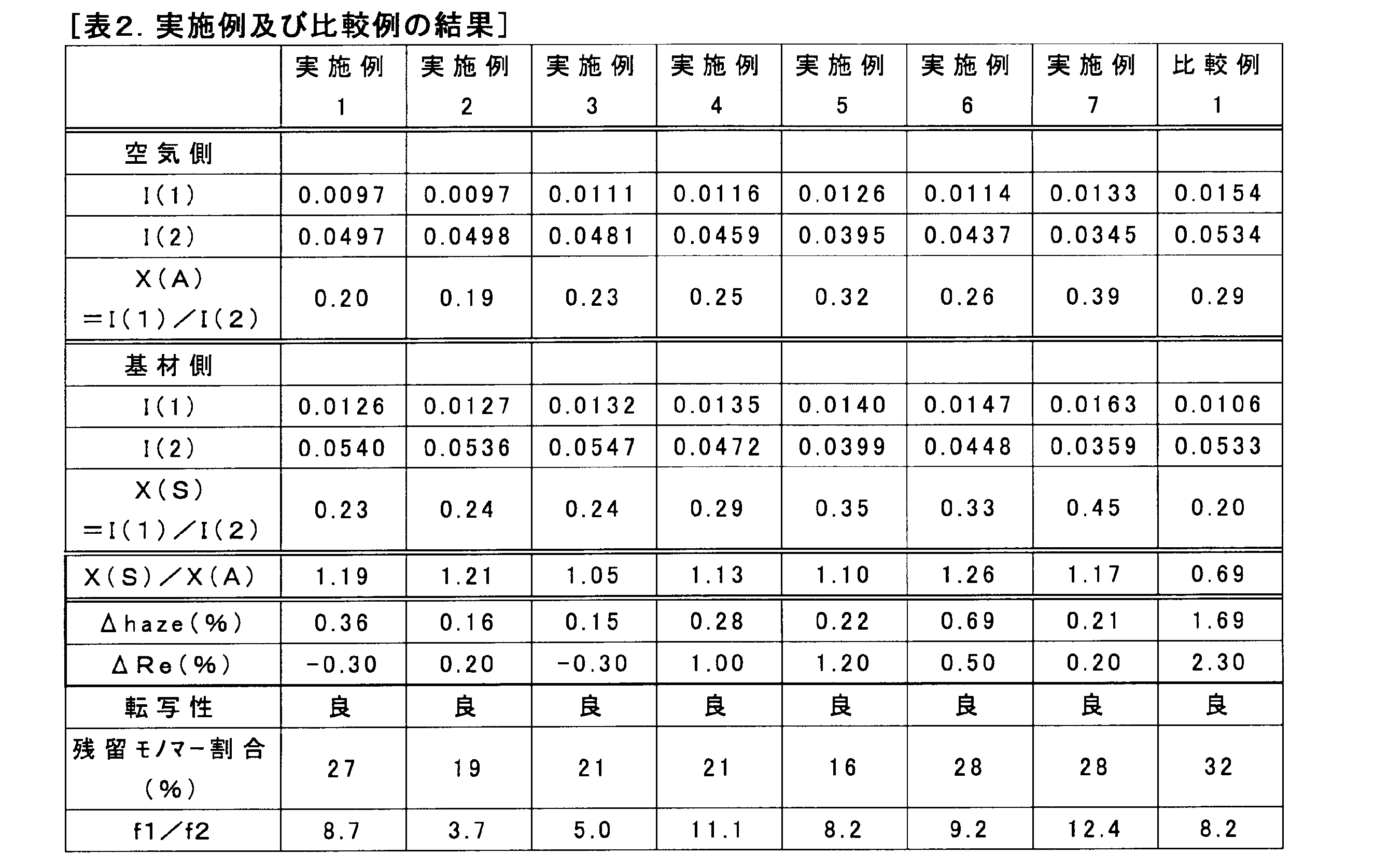
表2から分かるように、X(S)/X(A)が式(i)を満たす実施例1~7においては、Δhazeが小さく、耐傷付き性を改善できている。また、実施例1~7においては、ΔReの絶対値が小さいことから、得られた液晶硬化層が、優れた接着剤耐性を有していることが分かる。
110 液晶硬化層
120 基材フィルム
Claims (7)
- エチレン性不飽和結合及び芳香環を含有し逆波長分散性の複屈折を発現しうる重合性液晶化合物を含む液晶性組成物の硬化物からなる液晶硬化層を備えた、液晶硬化フィルムであって、
下記式(i):
1.00<X(S)/X(A) (i)
(前記の式(i)において、
X(S)は、前記液晶硬化層の一方の面のピーク比Xを表し、
X(A)は、前記液晶硬化層の他方の面のピーク比Xを表し、
ピーク比Xは、X=I(1)/I(2)で表される比を表し、
I(1)は、赤外全反射吸収スペクトル測定によるエチレン性不飽和結合の面内変角振動由来のピーク強度を表し、
I(2)は、赤外全反射吸収スペクトル測定による芳香環の不飽和結合の伸縮振動由来のピーク強度を表す。)
を満たす、液晶硬化フィルム。 - 前記液晶硬化層が、逆波長分散性のレターデーションを有する、請求項1記載の液晶硬化フィルム。
- 前記液晶性組成物が、界面活性剤を含み、
前記液晶硬化層の前記一方の面での前記界面活性剤の量が、前記液晶硬化層の前記他方の面での前記界面活性剤の量よりも、少ない、請求項1又は2記載の液晶硬化フィルム。 - 前記重合性液晶化合物が、前記重合性液晶化合物の分子中に、主鎖メソゲンと、前記主鎖メソゲンに結合した側鎖メソゲンとを含む、請求項1~3のいずれか一項に記載の液晶硬化フィルム。
- 前記重合性液晶化合物が、下記式(I)で表される、請求項1~4のいずれか一項に記載の液晶硬化フィルム。
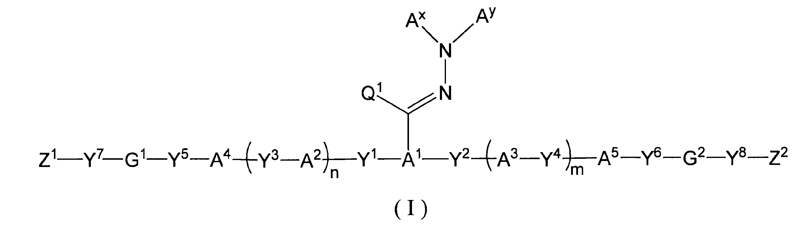
Y1~Y8は、それぞれ独立して、化学的な単結合、-O-、-S-、-O-C(=O)-、-C(=O)-O-、-O-C(=O)-O-、-NR1-C(=O)-、-C(=O)-NR1-、-O-C(=O)-NR1-、-NR1-C(=O)-O-、-NR1-C(=O)-NR1-、-O-NR1-、又は、-NR1-O-を表す。ここで、R1は、水素原子又は炭素数1~6のアルキル基を表す。
G1、G2は、それぞれ独立して、置換基を有していてもよい、炭素数1~20の二価の脂肪族基を表す。また、前記脂肪族基には、1つの脂肪族基当たり1以上の-O-、-S-、-O-C(=O)-、-C(=O)-O-、-O-C(=O)-O-、-NR2-C(=O)-、-C(=O)-NR2-、-NR2-、又は、-C(=O)-が介在していてもよい。ただし、-O-又は-S-がそれぞれ2以上隣接して介在する場合を除く。ここで、R2は、水素原子又は炭素数1~6のアルキル基を表す。
Z1、Z2は、それぞれ独立して、ハロゲン原子で置換されていてもよい炭素数2~10のアルケニル基を表す。
Axは、芳香族炭化水素環及び芳香族複素環からなる群から選ばれる少なくとも一つの芳香環を有する、炭素数2~30の有機基を表す。
Ayは、水素原子、置換基を有していてもよい炭素数1~20のアルキル基、置換基を有していてもよい炭素数2~20のアルケニル基、置換基を有していてもよい炭素数3~12のシクロアルキル基、置換基を有していてもよい炭素数2~20のアルキニル基、-C(=O)-R3、-SO2-R4、-C(=S)NH-R9、又は、芳香族炭化水素環及び芳香族複素環からなる群から選ばれる少なくとも一つの芳香環を有する、炭素数2~30の有機基を表す。ここで、R3は、置換基を有していてもよい炭素数1~20のアルキル基、置換基を有していてもよい炭素数2~20のアルケニル基、置換基を有していてもよい炭素数3~12のシクロアルキル基、又は、炭素数5~12の芳香族炭化水素環基を表す。R4は、炭素数1~20のアルキル基、炭素数2~20のアルケニル基、フェニル基、又は、4-メチルフェニル基を表す。R9は、置換基を有していてもよい炭素数1~20のアルキル基、置換基を有していてもよい炭素数2~20のアルケニル基、置換基を有していてもよい炭素数3~12のシクロアルキル基、又は、置換基を有していてもよい炭素数5~20の芳香族基を表す。前記Ax及びAyが有する芳香環は、置換基を有していてもよい。また、前記AxとAyは、一緒になって、環を形成していてもよい。
A1は、置換基を有していてもよい三価の芳香族基を表す。
A2、A3は、それぞれ独立して、置換基を有していてもよい炭素数3~30の二価の脂環式炭化水素基を表す。
A4、A5は、それぞれ独立して、置換基を有していてもよい、炭素数6~30の二価の芳香族基を表す。
Q1は、水素原子、又は、置換基を有していてもよい炭素数1~6のアルキル基を表す。
m及びnは、それぞれ独立に、0又は1を表す。) - 前記重合性液晶化合物が、前記重合性液晶化合物の分子中に、ベンゾチアゾール環、並びに、シクロヘキシル環及びフェニル環の組み合わせ、からなる群より選ばれる少なくとも1種を含有する、請求項1~5のいずれか一項に記載の液晶硬化フィルム。
- 請求項1~6のいずれか一項に記載の液晶硬化フィルムの製造方法であって、
基材フィルム上に、前記液晶性組成物の層を形成する工程と、
前記液晶性組成物の層を硬化させて、液晶硬化層を得る工程と、を含む、液晶硬化フィルムの製造方法。
Priority Applications (4)
| Application Number | Priority Date | Filing Date | Title |
|---|---|---|---|
| CN201780017958.3A CN108780185A (zh) | 2016-03-28 | 2017-03-09 | 液晶固化膜及其制造方法 |
| JP2018508919A JP6844615B2 (ja) | 2016-03-28 | 2017-03-09 | 液晶硬化フィルム及びその製造方法 |
| KR1020187027104A KR20180127351A (ko) | 2016-03-28 | 2017-03-09 | 액정 경화 필름 및 그 제조 방법 |
| US16/084,692 US20190071604A1 (en) | 2016-03-28 | 2017-03-09 | Liquid crystal cured film and method for manufacturing same |
Applications Claiming Priority (2)
| Application Number | Priority Date | Filing Date | Title |
|---|---|---|---|
| JP2016064047 | 2016-03-28 | ||
| JP2016-064047 | 2016-03-28 |
Publications (1)
| Publication Number | Publication Date |
|---|---|
| WO2017169637A1 true WO2017169637A1 (ja) | 2017-10-05 |
Family
ID=59963065
Family Applications (1)
| Application Number | Title | Priority Date | Filing Date |
|---|---|---|---|
| PCT/JP2017/009542 Ceased WO2017169637A1 (ja) | 2016-03-28 | 2017-03-09 | 液晶硬化フィルム及びその製造方法 |
Country Status (6)
| Country | Link |
|---|---|
| US (1) | US20190071604A1 (ja) |
| JP (1) | JP6844615B2 (ja) |
| KR (1) | KR20180127351A (ja) |
| CN (1) | CN108780185A (ja) |
| TW (1) | TWI709486B (ja) |
| WO (1) | WO2017169637A1 (ja) |
Cited By (5)
| Publication number | Priority date | Publication date | Assignee | Title |
|---|---|---|---|---|
| WO2019116990A1 (ja) * | 2017-12-12 | 2019-06-20 | 日本ゼオン株式会社 | 液晶配向層及びその製造方法、光学フィルム及びその製造方法、1/4波長板、偏光板並びに有機エレクトロルミネッセンス表示パネル |
| JP2020034871A (ja) * | 2018-08-31 | 2020-03-05 | 日本ゼオン株式会社 | 液晶硬化フィルム及びその製造方法、偏光板並びに有機エレクトロルミネッセンス表示装置 |
| JP2020038242A (ja) * | 2018-08-31 | 2020-03-12 | 日本ゼオン株式会社 | 液晶硬化フィルム、偏光板及び有機エレクトロルミネッセンス表示装置の製造方法 |
| US20220288827A1 (en) * | 2019-12-02 | 2022-09-15 | Fujifilm Corporation | Liquid crystal film for three-dimensional molding, three-dimensional molded body, and method of manufacturing three-dimensional molded body |
| WO2026070581A1 (ja) * | 2024-09-27 | 2026-04-02 | 富士フイルム株式会社 | フィルム、偏光板、画像表示装置 |
Families Citing this family (2)
| Publication number | Priority date | Publication date | Assignee | Title |
|---|---|---|---|---|
| WO2017154598A1 (ja) * | 2016-03-08 | 2017-09-14 | 日本ゼオン株式会社 | 液晶性組成物、液晶硬化層及びその液晶硬化層の製造方法 |
| US11702595B2 (en) | 2019-06-28 | 2023-07-18 | Rolic Technologies AG | Polymerizable liquid crystal |
Citations (7)
| Publication number | Priority date | Publication date | Assignee | Title |
|---|---|---|---|---|
| JP2004125841A (ja) * | 2002-09-30 | 2004-04-22 | Fuji Photo Film Co Ltd | 位相差板、その製造方法およびそれを用いた円偏光板 |
| JP2007249108A (ja) * | 2006-03-20 | 2007-09-27 | Fujifilm Corp | 光学補償シートならびに、これを用いた偏光板および液晶表示装置 |
| JP2007299006A (ja) * | 2007-06-25 | 2007-11-15 | Dainippon Printing Co Ltd | 液晶性転写体 |
| JP2008009156A (ja) * | 2006-06-29 | 2008-01-17 | Nitto Denko Corp | 粘着型光学フィルムの製造方法、粘着型光学フィルムおよび画像表示装置 |
| JP2015143786A (ja) * | 2014-01-31 | 2015-08-06 | 住友化学株式会社 | 液晶硬化膜 |
| JP2016012031A (ja) * | 2014-06-27 | 2016-01-21 | 日本ゼオン株式会社 | 複層フィルムの製造方法、位相差フィルム、円偏光板、及び、有機エレクトロルミネッセンス表示装置 |
| KR20160026738A (ko) * | 2014-08-29 | 2016-03-09 | 스미또모 가가꾸 가부시키가이샤 | 광학 필름의 제조 방법 |
Family Cites Families (4)
| Publication number | Priority date | Publication date | Assignee | Title |
|---|---|---|---|---|
| JP5905419B2 (ja) * | 2013-03-13 | 2016-04-20 | 富士フイルム株式会社 | 重合性液晶化合物、液晶組成物、高分子材料とその製造方法、フィルム、偏光板および液晶表示装置 |
| JP2015143790A (ja) * | 2014-01-31 | 2015-08-06 | 住友化学株式会社 | 転写用光学異方性シート |
| JP2015143789A (ja) * | 2014-01-31 | 2015-08-06 | 住友化学株式会社 | 転写用光学異方性シート |
| JP2016091022A (ja) * | 2014-10-31 | 2016-05-23 | 住友化学株式会社 | 光学異方性フィルム及び光学異方性フィルムの製造方法 |
-
2017
- 2017-03-09 US US16/084,692 patent/US20190071604A1/en not_active Abandoned
- 2017-03-09 KR KR1020187027104A patent/KR20180127351A/ko not_active Ceased
- 2017-03-09 JP JP2018508919A patent/JP6844615B2/ja active Active
- 2017-03-09 WO PCT/JP2017/009542 patent/WO2017169637A1/ja not_active Ceased
- 2017-03-09 CN CN201780017958.3A patent/CN108780185A/zh active Pending
- 2017-03-16 TW TW106108672A patent/TWI709486B/zh not_active IP Right Cessation
Patent Citations (7)
| Publication number | Priority date | Publication date | Assignee | Title |
|---|---|---|---|---|
| JP2004125841A (ja) * | 2002-09-30 | 2004-04-22 | Fuji Photo Film Co Ltd | 位相差板、その製造方法およびそれを用いた円偏光板 |
| JP2007249108A (ja) * | 2006-03-20 | 2007-09-27 | Fujifilm Corp | 光学補償シートならびに、これを用いた偏光板および液晶表示装置 |
| JP2008009156A (ja) * | 2006-06-29 | 2008-01-17 | Nitto Denko Corp | 粘着型光学フィルムの製造方法、粘着型光学フィルムおよび画像表示装置 |
| JP2007299006A (ja) * | 2007-06-25 | 2007-11-15 | Dainippon Printing Co Ltd | 液晶性転写体 |
| JP2015143786A (ja) * | 2014-01-31 | 2015-08-06 | 住友化学株式会社 | 液晶硬化膜 |
| JP2016012031A (ja) * | 2014-06-27 | 2016-01-21 | 日本ゼオン株式会社 | 複層フィルムの製造方法、位相差フィルム、円偏光板、及び、有機エレクトロルミネッセンス表示装置 |
| KR20160026738A (ko) * | 2014-08-29 | 2016-03-09 | 스미또모 가가꾸 가부시키가이샤 | 광학 필름의 제조 방법 |
Cited By (9)
| Publication number | Priority date | Publication date | Assignee | Title |
|---|---|---|---|---|
| WO2019116990A1 (ja) * | 2017-12-12 | 2019-06-20 | 日本ゼオン株式会社 | 液晶配向層及びその製造方法、光学フィルム及びその製造方法、1/4波長板、偏光板並びに有機エレクトロルミネッセンス表示パネル |
| JPWO2019116990A1 (ja) * | 2017-12-12 | 2021-01-07 | 日本ゼオン株式会社 | 液晶配向層及びその製造方法、光学フィルム及びその製造方法、1/4波長板、偏光板並びに有機エレクトロルミネッセンス表示パネル |
| JP7363483B2 (ja) | 2017-12-12 | 2023-10-18 | 日本ゼオン株式会社 | 光学フィルム及びその製造方法、1/4波長板、偏光板並びに有機エレクトロルミネッセンス表示パネル |
| JP2020034871A (ja) * | 2018-08-31 | 2020-03-05 | 日本ゼオン株式会社 | 液晶硬化フィルム及びその製造方法、偏光板並びに有機エレクトロルミネッセンス表示装置 |
| JP2020038242A (ja) * | 2018-08-31 | 2020-03-12 | 日本ゼオン株式会社 | 液晶硬化フィルム、偏光板及び有機エレクトロルミネッセンス表示装置の製造方法 |
| US20220288827A1 (en) * | 2019-12-02 | 2022-09-15 | Fujifilm Corporation | Liquid crystal film for three-dimensional molding, three-dimensional molded body, and method of manufacturing three-dimensional molded body |
| JP2023171833A (ja) * | 2019-12-02 | 2023-12-05 | 富士フイルム株式会社 | 三次元成形用液晶フィルム、三次元成形体、および、三次元成形体の製造方法 |
| JP7712335B2 (ja) | 2019-12-02 | 2025-07-23 | 富士フイルム株式会社 | 三次元成形用液晶フィルム、三次元成形体、および、三次元成形体の製造方法 |
| WO2026070581A1 (ja) * | 2024-09-27 | 2026-04-02 | 富士フイルム株式会社 | フィルム、偏光板、画像表示装置 |
Also Published As
| Publication number | Publication date |
|---|---|
| CN108780185A (zh) | 2018-11-09 |
| KR20180127351A (ko) | 2018-11-28 |
| JP6844615B2 (ja) | 2021-03-17 |
| JPWO2017169637A1 (ja) | 2019-01-31 |
| TW201801925A (zh) | 2018-01-16 |
| TWI709486B (zh) | 2020-11-11 |
| US20190071604A1 (en) | 2019-03-07 |
Similar Documents
| Publication | Publication Date | Title |
|---|---|---|
| CN104995219B (zh) | 聚合性化合物、聚合性组合物、高分子、以及光学各向异性体 | |
| CN107406769B (zh) | 液晶性组合物、相位差层的制造方法和圆偏振片 | |
| WO2017169637A1 (ja) | 液晶硬化フィルム及びその製造方法 | |
| WO2016171041A1 (ja) | 複層フィルムの製造方法及び複層フィルム | |
| JP6442886B2 (ja) | 複層フィルム、位相差フィルム、円偏光板、及び、有機エレクトロルミネッセンス表示装置の製造方法 | |
| JP6641683B2 (ja) | 樹脂フィルム、λ/4板、円偏光板、有機エレクトロルミネッセンス表示装置、及び製造方法 | |
| WO2017154598A1 (ja) | 液晶性組成物、液晶硬化層及びその液晶硬化層の製造方法 | |
| JPWO2017110638A1 (ja) | 液晶性組成物、液晶硬化層及びその製造方法、並びに、光学フィルム | |
| WO2017057005A1 (ja) | 光学フィルム及びその製造方法 | |
| US20180370184A1 (en) | Optical anisotropic layer and manufacturing method therefor, optical anisotropic laminate, and circularly polarizing plate | |
| WO2018173778A1 (ja) | 液晶組成物、液晶硬化フィルム及びその製造方法 | |
| WO2018173773A1 (ja) | 液晶硬化フィルム及びその製造方法 | |
| JP6446860B2 (ja) | 複層フィルム、位相差フィルム、円偏光板、及び、有機エレクトロルミネッセンス表示装置の製造方法 | |
| JP2018163218A (ja) | 液晶硬化フィルム及びその製造方法 |
Legal Events
| Date | Code | Title | Description |
|---|---|---|---|
| ENP | Entry into the national phase |
Ref document number: 2018508919 Country of ref document: JP Kind code of ref document: A |
|
| ENP | Entry into the national phase |
Ref document number: 20187027104 Country of ref document: KR Kind code of ref document: A |
|
| NENP | Non-entry into the national phase |
Ref country code: DE |
|
| 121 | Ep: the epo has been informed by wipo that ep was designated in this application |
Ref document number: 17774182 Country of ref document: EP Kind code of ref document: A1 |
|
| 122 | Ep: pct application non-entry in european phase |
Ref document number: 17774182 Country of ref document: EP Kind code of ref document: A1 |