WO2017168522A1 - Convertisseur de puissance - Google Patents
Convertisseur de puissance Download PDFInfo
- Publication number
- WO2017168522A1 WO2017168522A1 PCT/JP2016/059931 JP2016059931W WO2017168522A1 WO 2017168522 A1 WO2017168522 A1 WO 2017168522A1 JP 2016059931 W JP2016059931 W JP 2016059931W WO 2017168522 A1 WO2017168522 A1 WO 2017168522A1
- Authority
- WO
- WIPO (PCT)
- Prior art keywords
- voltage
- phase
- inverter
- offset
- offset voltage
- Prior art date
Links
Images


Classifications
-
- H—ELECTRICITY
- H02—GENERATION; CONVERSION OR DISTRIBUTION OF ELECTRIC POWER
- H02M—APPARATUS FOR CONVERSION BETWEEN AC AND AC, BETWEEN AC AND DC, OR BETWEEN DC AND DC, AND FOR USE WITH MAINS OR SIMILAR POWER SUPPLY SYSTEMS; CONVERSION OF DC OR AC INPUT POWER INTO SURGE OUTPUT POWER; CONTROL OR REGULATION THEREOF
- H02M7/00—Conversion of ac power input into dc power output; Conversion of dc power input into ac power output
- H02M7/42—Conversion of dc power input into ac power output without possibility of reversal
- H02M7/44—Conversion of dc power input into ac power output without possibility of reversal by static converters
- H02M7/48—Conversion of dc power input into ac power output without possibility of reversal by static converters using discharge tubes with control electrode or semiconductor devices with control electrode
- H02M7/53—Conversion of dc power input into ac power output without possibility of reversal by static converters using discharge tubes with control electrode or semiconductor devices with control electrode using devices of a triode or transistor type requiring continuous application of a control signal
- H02M7/537—Conversion of dc power input into ac power output without possibility of reversal by static converters using discharge tubes with control electrode or semiconductor devices with control electrode using devices of a triode or transistor type requiring continuous application of a control signal using semiconductor devices only, e.g. single switched pulse inverters
- H02M7/539—Conversion of dc power input into ac power output without possibility of reversal by static converters using discharge tubes with control electrode or semiconductor devices with control electrode using devices of a triode or transistor type requiring continuous application of a control signal using semiconductor devices only, e.g. single switched pulse inverters with automatic control of output wave form or frequency
- H02M7/5395—Conversion of dc power input into ac power output without possibility of reversal by static converters using discharge tubes with control electrode or semiconductor devices with control electrode using devices of a triode or transistor type requiring continuous application of a control signal using semiconductor devices only, e.g. single switched pulse inverters with automatic control of output wave form or frequency by pulse-width modulation
-
- G—PHYSICS
- G01—MEASURING; TESTING
- G01R—MEASURING ELECTRIC VARIABLES; MEASURING MAGNETIC VARIABLES
- G01R31/00—Arrangements for testing electric properties; Arrangements for locating electric faults; Arrangements for electrical testing characterised by what is being tested not provided for elsewhere
- G01R31/40—Testing power supplies
- G01R31/42—AC power supplies
-
- H—ELECTRICITY
- H02—GENERATION; CONVERSION OR DISTRIBUTION OF ELECTRIC POWER
- H02H—EMERGENCY PROTECTIVE CIRCUIT ARRANGEMENTS
- H02H7/00—Emergency protective circuit arrangements specially adapted for specific types of electric machines or apparatus or for sectionalised protection of cable or line systems, and effecting automatic switching in the event of an undesired change from normal working conditions
- H02H7/10—Emergency protective circuit arrangements specially adapted for specific types of electric machines or apparatus or for sectionalised protection of cable or line systems, and effecting automatic switching in the event of an undesired change from normal working conditions for converters; for rectifiers
- H02H7/12—Emergency protective circuit arrangements specially adapted for specific types of electric machines or apparatus or for sectionalised protection of cable or line systems, and effecting automatic switching in the event of an undesired change from normal working conditions for converters; for rectifiers for static converters or rectifiers
- H02H7/122—Emergency protective circuit arrangements specially adapted for specific types of electric machines or apparatus or for sectionalised protection of cable or line systems, and effecting automatic switching in the event of an undesired change from normal working conditions for converters; for rectifiers for static converters or rectifiers for inverters, i.e. dc/ac converters
- H02H7/1225—Emergency protective circuit arrangements specially adapted for specific types of electric machines or apparatus or for sectionalised protection of cable or line systems, and effecting automatic switching in the event of an undesired change from normal working conditions for converters; for rectifiers for static converters or rectifiers for inverters, i.e. dc/ac converters responsive to internal faults, e.g. shoot-through
-
- H—ELECTRICITY
- H02—GENERATION; CONVERSION OR DISTRIBUTION OF ELECTRIC POWER
- H02M—APPARATUS FOR CONVERSION BETWEEN AC AND AC, BETWEEN AC AND DC, OR BETWEEN DC AND DC, AND FOR USE WITH MAINS OR SIMILAR POWER SUPPLY SYSTEMS; CONVERSION OF DC OR AC INPUT POWER INTO SURGE OUTPUT POWER; CONTROL OR REGULATION THEREOF
- H02M1/00—Details of apparatus for conversion
- H02M1/08—Circuits specially adapted for the generation of control voltages for semiconductor devices incorporated in static converters
-
- H—ELECTRICITY
- H02—GENERATION; CONVERSION OR DISTRIBUTION OF ELECTRIC POWER
- H02M—APPARATUS FOR CONVERSION BETWEEN AC AND AC, BETWEEN AC AND DC, OR BETWEEN DC AND DC, AND FOR USE WITH MAINS OR SIMILAR POWER SUPPLY SYSTEMS; CONVERSION OF DC OR AC INPUT POWER INTO SURGE OUTPUT POWER; CONTROL OR REGULATION THEREOF
- H02M1/00—Details of apparatus for conversion
- H02M1/38—Means for preventing simultaneous conduction of switches
-
- H—ELECTRICITY
- H02—GENERATION; CONVERSION OR DISTRIBUTION OF ELECTRIC POWER
- H02M—APPARATUS FOR CONVERSION BETWEEN AC AND AC, BETWEEN AC AND DC, OR BETWEEN DC AND DC, AND FOR USE WITH MAINS OR SIMILAR POWER SUPPLY SYSTEMS; CONVERSION OF DC OR AC INPUT POWER INTO SURGE OUTPUT POWER; CONTROL OR REGULATION THEREOF
- H02M7/00—Conversion of ac power input into dc power output; Conversion of dc power input into ac power output
- H02M7/42—Conversion of dc power input into ac power output without possibility of reversal
- H02M7/44—Conversion of dc power input into ac power output without possibility of reversal by static converters
- H02M7/48—Conversion of dc power input into ac power output without possibility of reversal by static converters using discharge tubes with control electrode or semiconductor devices with control electrode
- H02M7/53—Conversion of dc power input into ac power output without possibility of reversal by static converters using discharge tubes with control electrode or semiconductor devices with control electrode using devices of a triode or transistor type requiring continuous application of a control signal
- H02M7/537—Conversion of dc power input into ac power output without possibility of reversal by static converters using discharge tubes with control electrode or semiconductor devices with control electrode using devices of a triode or transistor type requiring continuous application of a control signal using semiconductor devices only, e.g. single switched pulse inverters
- H02M7/5387—Conversion of dc power input into ac power output without possibility of reversal by static converters using discharge tubes with control electrode or semiconductor devices with control electrode using devices of a triode or transistor type requiring continuous application of a control signal using semiconductor devices only, e.g. single switched pulse inverters in a bridge configuration
- H02M7/53871—Conversion of dc power input into ac power output without possibility of reversal by static converters using discharge tubes with control electrode or semiconductor devices with control electrode using devices of a triode or transistor type requiring continuous application of a control signal using semiconductor devices only, e.g. single switched pulse inverters in a bridge configuration with automatic control of output voltage or current
- H02M7/53875—Conversion of dc power input into ac power output without possibility of reversal by static converters using discharge tubes with control electrode or semiconductor devices with control electrode using devices of a triode or transistor type requiring continuous application of a control signal using semiconductor devices only, e.g. single switched pulse inverters in a bridge configuration with automatic control of output voltage or current with analogue control of three-phase output
-
- G—PHYSICS
- G01—MEASURING; TESTING
- G01R—MEASURING ELECTRIC VARIABLES; MEASURING MAGNETIC VARIABLES
- G01R31/00—Arrangements for testing electric properties; Arrangements for locating electric faults; Arrangements for electrical testing characterised by what is being tested not provided for elsewhere
- G01R31/50—Testing of electric apparatus, lines, cables or components for short-circuits, continuity, leakage current or incorrect line connections
- G01R31/52—Testing for short-circuits, leakage current or ground faults
-
- H—ELECTRICITY
- H02—GENERATION; CONVERSION OR DISTRIBUTION OF ELECTRIC POWER
- H02M—APPARATUS FOR CONVERSION BETWEEN AC AND AC, BETWEEN AC AND DC, OR BETWEEN DC AND DC, AND FOR USE WITH MAINS OR SIMILAR POWER SUPPLY SYSTEMS; CONVERSION OF DC OR AC INPUT POWER INTO SURGE OUTPUT POWER; CONTROL OR REGULATION THEREOF
- H02M1/00—Details of apparatus for conversion
- H02M1/0003—Details of control, feedback or regulation circuits
- H02M1/0009—Devices or circuits for detecting current in a converter
-
- H—ELECTRICITY
- H02—GENERATION; CONVERSION OR DISTRIBUTION OF ELECTRIC POWER
- H02M—APPARATUS FOR CONVERSION BETWEEN AC AND AC, BETWEEN AC AND DC, OR BETWEEN DC AND DC, AND FOR USE WITH MAINS OR SIMILAR POWER SUPPLY SYSTEMS; CONVERSION OF DC OR AC INPUT POWER INTO SURGE OUTPUT POWER; CONTROL OR REGULATION THEREOF
- H02M1/00—Details of apparatus for conversion
- H02M1/0003—Details of control, feedback or regulation circuits
- H02M1/0025—Arrangements for modifying reference values, feedback values or error values in the control loop of a converter
-
- H—ELECTRICITY
- H02—GENERATION; CONVERSION OR DISTRIBUTION OF ELECTRIC POWER
- H02M—APPARATUS FOR CONVERSION BETWEEN AC AND AC, BETWEEN AC AND DC, OR BETWEEN DC AND DC, AND FOR USE WITH MAINS OR SIMILAR POWER SUPPLY SYSTEMS; CONVERSION OF DC OR AC INPUT POWER INTO SURGE OUTPUT POWER; CONTROL OR REGULATION THEREOF
- H02M1/00—Details of apparatus for conversion
- H02M1/44—Circuits or arrangements for compensating for electromagnetic interference in converters or inverters
-
- H—ELECTRICITY
- H02—GENERATION; CONVERSION OR DISTRIBUTION OF ELECTRIC POWER
- H02P—CONTROL OR REGULATION OF ELECTRIC MOTORS, ELECTRIC GENERATORS OR DYNAMO-ELECTRIC CONVERTERS; CONTROLLING TRANSFORMERS, REACTORS OR CHOKE COILS
- H02P27/00—Arrangements or methods for the control of AC motors characterised by the kind of supply voltage
- H02P27/04—Arrangements or methods for the control of AC motors characterised by the kind of supply voltage using variable-frequency supply voltage, e.g. inverter or converter supply voltage
- H02P27/06—Arrangements or methods for the control of AC motors characterised by the kind of supply voltage using variable-frequency supply voltage, e.g. inverter or converter supply voltage using dc to ac converters or inverters
- H02P27/08—Arrangements or methods for the control of AC motors characterised by the kind of supply voltage using variable-frequency supply voltage, e.g. inverter or converter supply voltage using dc to ac converters or inverters with pulse width modulation
Definitions
- the present invention relates to a power converter that converts a DC voltage into a three-phase voltage based on a three-phase voltage command and outputs the converted voltage.
- the modulation factor which is the amplitude of the duty command signal with respect to the power supply voltage
- the lower solid two-phase modulation or the upper solid two-phase modulation is used, and the modulation factor is equal to or lower than the first predetermined value.
- the voltage saturation using the three-phase modulation depends on the amplitude value of the inverter output voltage and the voltage phase from the reference direction of the voltage vector. Therefore, even in the case of an amplitude value that causes voltage saturation in three-phase modulation, voltage saturation is not always achieved, and voltage saturation does not occur depending on the voltage phase. Under such operating conditions, outputting three-phase modulation and two-phase modulation in accordance with the voltage phase is advantageous in reducing distortion of the output voltage, noise, and vibration.
- Patent Document 1 and Patent Document 2 always switch to two-phase modulation based on the amplitude or the modulation rate, respectively.
- the use of the two-phase modulation causes a problem that the distortion rate of the output voltage is deteriorated and the noise and vibration of the motor increase. is there.
- the noise and vibration of the motor increase due to the occurrence of discontinuous voltage changes.
- the present invention has been made to solve the above-described problems, and an object of the present invention is to obtain a power converter that can reduce the distortion rate of the output voltage and reduce noise and vibration.
- the power conversion device is a power conversion device that converts a DC voltage into a three-phase voltage based on a three-phase voltage command that is a sine wave and outputs the three-phase voltage command.
- the first offset voltage is calculated by subtracting the first DC voltage obtained by multiplying the DC voltage by the first constant from the maximum phase, and the sign of the first offset voltage is negative
- a first offset voltage calculator that sets the first offset voltage to 0, and a modified three-phase voltage command calculator that subtracts the first offset voltage from each phase of the three-phase voltage command and outputs a modified three-phase voltage command
- an inverter that outputs a three-phase voltage based on the modified three-phase voltage command.
- the first offset voltage calculator is configured to multiply the DC voltage by the first constant when the three-phase voltage command is set to the maximum phase, the intermediate phase, and the minimum phase in descending order.
- the first offset voltage is calculated by subtracting the voltage from the maximum phase, and when the sign of the first offset voltage is negative, the first offset voltage is set to 0.
- the first offset voltage is subtracted from each phase of the phase voltage command to output a modified three-phase voltage command. Therefore, the distortion rate of the output voltage can be reduced, and noise and vibration can be reduced.
- FIG. 3 is a flowchart illustrating a calculation of a first offset voltage calculation unit illustrated in FIG. 1. It is a flowchart which shows the calculation of the correction 3 phase voltage command calculating part shown in FIG. It is explanatory drawing which shows each output waveform of the power converter device which concerns on Embodiment 1 of this invention. It is explanatory drawing which shows each output waveform at the time of increasing the amplitude value of the three-phase voltage command in FIG. It is a whole block diagram which shows the power converter device which concerns on Embodiment 2 of this invention.
- FIG. 7 It is a block diagram which shows the output voltage detection circuit shown in FIG. It is a flowchart which shows operation
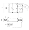
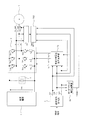
- FIG. 1 is an overall configuration diagram showing a power conversion apparatus according to Embodiment 1 of the present invention.
- an AC rotating machine 1 is an AC rotating machine having three-phase windings U, V, and W.
- a permanent magnet synchronous rotating machine for example, a permanent magnet synchronous rotating machine, a wound field synchronous rotating machine, an induction rotating machine, and synchronous reluctance Motors and the like.
- DC power supply 2 outputs DC voltage Vdc to inverter 3.
- the DC power supply includes all devices that output DC voltage, such as a battery, a DC-DC converter, a diode rectifier, and a PWM rectifier.
- Vdc 10V will be described.
- the inverter 3 performs PWM modulation with a carrier period Tc of, for example, 50 ⁇ s based on the corrected three-phase voltage commands Vu, Vv, Vw and the DC voltage Vdc input from the DC power supply 2, and the three-phase winding of the AC rotating machine 1. A voltage is applied to U, V, and W.
- switches Sup to Swn semiconductor switches such as IGBTs, bipolar transistors, and MOS power transistors and diodes connected in antiparallel are used.
- Current detection resistance elements Ru, Rv, and Rw are provided in series with the lower arm elements Sun, Svn, and Swn of the inverter 3, respectively.
- Ru detects the current flowing through the U-phase winding of the AC rotating machine 1 by acquiring the voltage at both ends when the Sun is turned on.
- Rv detects the current flowing through the V-phase winding of the AC rotating machine 1 by acquiring the voltage at both ends at the timing when Svn is turned on.
- Rw detects the current flowing through the W-phase winding of the AC rotating machine 1 by acquiring the voltage at both ends at the timing when Swn is turned on.
- the smoothing capacitor 4 is a capacitor that stabilizes the DC voltage Vdc of the DC power supply 2.
- the basic command calculation unit 5 calculates three-phase voltage commands Vub, Vvb, and Vwb for driving the AC rotating machine 1.
- V / which determines the amplitude of the three-phase voltage command after setting the speed (frequency) command f of the AC rotating machine 1 as the control command in FIG. F control is mentioned. Further, a current command of the AC rotating machine 1 is set as a control command, and the deviation is set to 0 based on a deviation between the current command and the current of the AC rotating machine 1 detected by the current detection resistance elements Ru, Rv, Rw. Therefore, a known technique such as current feedback control for calculating the three-phase voltage commands Vub, Vvb, Vwb by proportional-integral control is used.
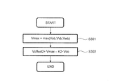
- the first offset voltage calculator 6a calculates the first offset voltage Voffset1 based on the three-phase voltage commands Vub, Vvb, and Vwb.
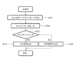
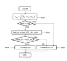
- FIG. 2 is a flowchart showing the calculation of the first offset voltage calculation unit 6a.
- the modified three-phase voltage command calculation unit 7a calculates the modified three-phase voltage commands Vu, Vv, and Vw based on the three-phase voltage commands Vub, Vvb, and Vwb and the first offset voltage Voffset1.
- FIG. 3 is a flowchart showing the calculation of the modified three-phase voltage command calculation unit 7a.
- Voffset1 is subtracted from each of Vub, Vvb, and Vwb to calculate Vu, Vv, and Vw.
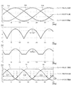
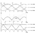
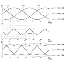
- FIG. 4 is an explanatory diagram showing output waveforms of the power conversion apparatus according to Embodiment 1 of the present invention.
- three-phase voltage commands Vub, Vvb, Vwb are shown in the first stage from the top
- the first offset voltage Voffset1 ′ is shown in the second stage
- the first offset voltage Voffset1 is shown in the third stage.
- the modified three-phase voltage commands Vu, Vv, and Vw are shown in FIG.
- the voltage range that can be output without saturating the modified three-phase voltage command is the 10V section of -5 to 5V, and -5V is the inverter output lower limit.
- 0V is the inverter output center value, and 5V is the inverter output upper limit value.
- the modified three-phase voltage commands Vu, Vv, Vw are within 10% below the upper limit of 5 V in the voltage range ⁇ 5 to 5 V that can be output by the inverter, that is, 4 If it is present at ⁇ 5 V, the energization time of the lower arm switching element becomes insufficient, and current detection cannot be performed by the current detection resistance elements Ru, Rv, Rw.
- the modified three-phase voltage command is the inverter output lower limit value. It must be in the range from -5V to 4V which is the upper limit of current detection. Therefore, the first offset voltage Voffset1 'is set so that the three-phase voltage commands Vub, Vvb, Vwb do not exceed 4V.
- offset is also caused when the sign of Voffset1 'is negative and Vmax is 4V or less. That is, offsets are also made in sections A1, A2, A3, and A4 in FIG. In this section, since Vmax is less than 4V, the maximum phase of the modified three-phase voltage command does not exceed 4V even if there is no offset, so that current detection is possible with the current detection resistance element.
- Voffset1 if the sign of Voffset1 'is negative, it is corrected to 0 and the value is set to Voffset1. Then, by subtracting Voffset1 from the three-phase voltage commands Vub, Vvb, and Vwb, the energizing time of the lower arm switching element in the maximum phase is detected only in the sections B1, B2, and B3 that require offset for current detection. It is corrected so as to coincide with the lower limit value at which current can be detected by the resistance element.
- the three-phase voltage commands Vub, Vvb, and Vwb are output as modified three-phase voltage commands Vu, Vv, and Vw as they are. Therefore, in the sections A1, A2, A3, and A4, the average values of the corrected three-phase voltages Vu, Vv, and Vw coincide with the inverter output center value, and the neutral point voltage becomes equal to half the capacitor voltage. Therefore, as described in Patent Document 2, the effect of reducing noise and vibration is obtained in the section.
- Patent Document 1 three-phase modulation and two-phase modulation are switched according to the amplitude value of the inverter output voltage.
- the amplitude value of the three-phase voltage command is expressed by the following equation (1).
- the amplitude value becomes 4.33V. It becomes a constant value in all sections.
- This value is equal to the point A indicated by the black circle in the first stage of FIG. 4, that is, the peak value of the three-phase voltage command. Therefore, since the amplitude value exceeds 4V, considering the lower limit of the energization time of the lower arm switching element that current detection is impossible at over 4V, two-phase modulation is selected in all sections shown in FIG. Noise and vibration will get worse.
- Patent Document 2 only the amplitude value in Patent Document 1 is changed to the modulation factor, and the energization time of the lower arm switching element is secured for the three-phase voltage command shown in the first stage of FIG. Therefore, the lower solid two-phase modulation must be selected.
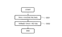
- an interval in which the maximum phase is an instantaneous value exceeding 4 V and an offset is required is determined in S103 in FIG. 2, and when it is unnecessary (Voffset1 ′ ⁇ 0), the first offset voltage Voffset1 is set to Voffset1 in S105. '( ⁇ 0) is corrected to 0 to obtain the final first offset voltage.
- the section that requires offset means that the three-phase voltage commands Vub, Vvb, and Vwb are used as the modified three-phase voltage commands Vu, Vv, and Vw, and the energization time of the lower arm switching element is the current detection resistance element. This is a case in which the maximum phase voltage of the corrected three-phase voltage command needs to be 4 V or less, which is a case where the value falls below the lower limit value that can be detected.
- the point voltage is equal to half the capacitor voltage.
- the modified three-phase voltage command must be in the range from ⁇ 4V, which is the current detection lower limit value, to 5V, which is the upper limit value of the inverter output.
- the third offset voltage Voffset3 ' is set so that the three-phase voltage commands Vub, Vvb, Vwb do not fall below -4V, which is the lower limit value at which current can be detected by the current detection resistor element.
- Voffset3 when the sign of Voffset3 ′ is positive, it is corrected to 0, and when it is negative, it is output as it is.
- the value is Voffset3, and Voffset3 is subtracted from the three-phase voltage commands Vub, Vvb, and Vwb as described above. Further, the same effect as that obtained when the current detection resistance elements Ru, Rv, and Rw are provided in series with the lower arm elements Sun, Svn, and Swn of the inverter 3 can be obtained.
- the first offset voltage calculator is configured to multiply the DC voltage by the first constant when the three-phase voltage command is set to the maximum phase, the intermediate phase, and the minimum phase in descending order. 1 DC voltage is subtracted from the maximum phase to calculate the first offset voltage, and when the sign of the first offset voltage is negative, the first offset voltage is set to 0, and the modified three-phase voltage command calculation unit The first offset voltage is subtracted from each phase of the three-phase voltage command to output a corrected three-phase voltage command.
- the use range of the three-phase modulation can be increased, and a discontinuous voltage change does not occur when the modulation method is switched. Therefore, the distortion rate of the output voltage can be reduced, and noise and vibration can be reduced.
- Embodiment 2 Compared to FIG. 4 in which the amplitude value of the three-phase voltage command is 4.33 V in the first embodiment, the three-phase voltage commands Vub, Vvb, when the amplitude value of the three-phase voltage command is increased to 5.48 V, FIG. 5 shows Vwb, the first offset voltage Voffset1 ′, the first offset voltage Voffset1, and the modified three-phase voltage commands Vu, Vv, and Vw.
- FIG. 6 is an overall configuration diagram showing a power converter according to Embodiment 2 of the present invention.
- the second embodiment differs from the first embodiment in a second offset voltage calculation unit 6b and a modified three-phase voltage command calculation unit 7b.
- the second offset voltage calculator 6b calculates the second offset voltage Voffset2 based on the three-phase voltage commands Vub, Vvb, and Vwb.
- FIG. 7 is a flowchart showing the calculation of the second offset voltage calculation unit 6b.
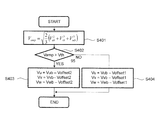
- the modified three-phase voltage command calculation unit 7b calculates the modified three-phase voltage commands Vu, Vv, and Vw based on the three-phase voltage commands Vub, Vvb, and Vwb, the first offset voltage Voffset1, and the second offset voltage Voffset2.
- FIG. 8 is a flowchart showing the calculation of the modified three-phase voltage command calculation unit 7b.
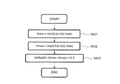
- the amplitude value Vamp of the three-phase voltage command is calculated by the above equation (1). Subsequently, in S402, it is determined whether the amplitude value Vamp is larger than the amplitude threshold value Vth.
- Voffset2 is subtracted from each of Vub, Vvb, and Vwb to calculate Vu, Vv, and Vw.
- Voffset1 is subtracted from each of Vub, Vvb, and Vwb to calculate Vu, Vv, and Vw.
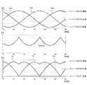
- FIG. 9 is an explanatory diagram showing output waveforms of the power conversion apparatus according to Embodiment 2 of the present invention.
- three-phase voltage commands Vub, Vvb and Vwb with the same amplitude value Vamp as in FIG. 5 at 5.48 V are shown in the first stage from the top, the second offset voltage Voffset2 is shown in the second stage, and the third stage
- the eyes show modified three-phase voltage commands Vu, Vv, and Vw.
- Vth 5V and “YES” is selected in the process of S402.
- the second offset voltage calculation unit is provided, and the second offset voltage obtained by subtracting the second DC voltage obtained by multiplying the DC voltage by the second constant from the maximum phase is 3 Since the output is performed when the amplitude of the phase voltage command is larger than the threshold, in addition to the effect of the first embodiment, voltage saturation can be avoided even when the amplitude of the three-phase voltage command is large, and the output voltage distortion can be avoided. In addition, noise and vibration can be reduced.
- a corrected three-phase voltage command is calculated based on the first offset voltage in the intervals C1, C2, C3, and C4. In other intervals, the corrected three-phase voltage command is calculated based on the second offset voltage. It goes without saying that the same effect can be obtained by calculating.
- the fourth offset voltage Voffset4 is calculated by subtracting the fifth DC voltage obtained by multiplying the fifth constant K5 by Vmax from Vmax.
- Embodiment 3 FIG.
- the third embodiment differs from the second embodiment in the second offset voltage calculation unit 6b.
- the second offset voltage calculator 6b calculates the second offset voltage Voffset2 based on the three-phase voltage commands Vub, Vvb, and Vwb.
- FIG. 10 is a flowchart showing the calculation of the second offset voltage calculation unit 6b.
- FIG. 11 is an explanatory diagram showing output waveforms of the power conversion apparatus according to Embodiment 3 of the present invention.
- the three-phase voltage commands Vub, Vvb, and Vwb in which the same amplitude value Vamp as in FIG. 5 is 5.48V are shown in the first stage from the top, the second offset voltage Voffset2 is shown in the second stage, and the third stage
- the eyes show modified three-phase voltage commands Vu, Vv, and Vw.
- Vth 5V and “YES” is selected in the process of S402 of FIG.
- the corrected three-phase voltage command is within the inverter output range, and voltage saturation can be avoided even when the amplitude is large.
- the second offset voltage calculation unit obtains the second offset voltage obtained by adding the third DC voltage obtained by multiplying the DC voltage by the third constant to the minimum phase.
- a corrected three-phase voltage command is calculated based on the first offset voltage in the intervals C1, C2, C3, and C4. In other intervals, the corrected three-phase voltage command is calculated based on the second offset voltage. It goes without saying that the same effect can be obtained by calculating.
- the fourth offset voltage Voffset4 is calculated by adding the sixth DC voltage obtained by multiplying the sixth constant K6 to Vmim.
- Embodiment 4 FIG.
- the fourth embodiment differs from the second embodiment in the second offset voltage calculation unit 6b.
- the second offset voltage calculator 6b calculates the second offset voltage Voffset2 based on the three-phase voltage commands Vub, Vvb, and Vwb.
- FIG. 12 is a flowchart showing the calculation of the second offset voltage calculation unit 6b.
- FIG. 13 is an explanatory diagram showing output waveforms of the power conversion apparatus according to Embodiment 4 of the present invention.
- the three-phase voltage commands Vub, Vvb, and Vwb in which the same amplitude value Vamp as in FIG. 5 is 5.48V are shown in the first stage from the top, the second offset voltage Voffset2 is shown in the second stage, and the third stage
- the eyes show modified three-phase voltage commands Vu, Vv, and Vw.
- Vth 5V and “YES” is selected in the process of S402 of FIG.
- the corrected three-phase voltage command is within the inverter output range, and voltage saturation can be avoided even when the amplitude is large.
- the second offset voltage calculation unit obtains the second offset voltage obtained by averaging the minimum phase and the maximum phase
- the amplitude of the three-phase voltage command is larger than the threshold value.
- the amplitude of the three-phase voltage command is large, voltage saturation can be avoided and output voltage distortion, noise, and vibration can be reduced. is there.
- a corrected three-phase voltage command is calculated based on the first offset voltage in the intervals C1, C2, C3, and C4. In other intervals, the corrected three-phase voltage command is calculated based on the second offset voltage. It goes without saying that the same effect can be obtained by calculating.
- the second offset voltage Voffset2 is calculated based on at least two of the maximum phase Vmax, the minimum phase Vmin, and the DC voltage Vdc, and the amplitude value Vamp of the three-phase voltage command is a threshold value. If the second offset voltage is subtracted from the three-phase voltage command when Vth is greater than Vth, voltage saturation can be avoided even when the amplitude of the three-phase voltage command is large, output voltage distortion, noise, It is possible to reduce vibration.
- the fourth offset voltage Voffset4 is calculated based on at least two of the maximum phase Vmax, the minimum phase Vmin, and the DC voltage Vdc, and the amplitude value Vamp of the three-phase voltage command is a threshold value. If the fourth offset voltage is subtracted from the three-phase voltage command when Vth is greater than Vth, voltage saturation can be avoided even when the amplitude of the three-phase voltage command is large, output voltage distortion, noise, It is possible to reduce vibration.
- FIG. 14 is an overall configuration diagram showing a power conversion device according to Embodiment 5 of the present invention.
- the fifth embodiment differs from the first embodiment in output voltage detection circuits 501, 502, and 503 and an inverter failure detection unit 504.
- the output voltage detection circuit 501 is a circuit that inputs Vu_real among the three-phase voltages Vu_real, Vv_real, and Vw_real output from the inverter 3 and outputs an on-time Tu of Vu_real.
- the output voltage detection circuit 502 is a circuit that inputs Vv_real among the three-phase voltages Vu_real, Vv_real, and Vw_real output from the inverter 3 and outputs an ON time Tv of Vv_real.
- the output voltage detection circuit 503 is a circuit that inputs Vw_real among the three-phase voltages Vu_real, Vv_real, and Vw_real output from the inverter 3 and outputs an ON time Tw of Vw_real.
- the on-time is the time connected to the upper arm switching element
- the off-time is the time connected to the lower arm element.
- FIG. 15 is an explanatory diagram showing the operation of the output voltage detection circuit shown in FIG. Note that the operation of the output voltage detection circuits 502 and 503 is the same as that of the output voltage detection circuit 501, and therefore will be omitted.
- Vu_real is a PWM waveform with a carrier period Tc, and is connected to the switch Sun during the off period and outputs 0 V, and is connected to the switch Sup during the on period and outputs Vdc [V].
- a threshold value Vth2 satisfying 0 ⁇ Vth2 ⁇ Vdc is set.
- Vu_real is larger than Vth2
- the count is increased, and when it is smaller, the count is held.
- the on-time Tu is counted and output to the inverter failure detection unit 504.
- FIG. 16 is a flowchart showing the operation of the inverter failure detection unit 504.
- the U-phase output voltage Vu_real2 is calculated by Tu ⁇ Tc ⁇ Vdc ⁇ 0.5Vdc using the on-time Tu, carrier cycle Tc, and DC voltage Vdc output from the output voltage detection circuit 501. To do. Subsequently, in S702, Vu output from the modified three-phase voltage command calculation unit 7a is subtracted from Vu_real2 obtained in S701 to calculate a U-phase voltage error Vu_err.
- the error reference value V_err_th is a value having a slight allowance in consideration that an error due to dead time or the like is included between the corrected three-phase voltage command and the voltage actually output from the inverter 3.
- , the W phase voltage error of the V phase and the W phase based on the V phase on time Tv and the W phase on time Tw respectively
- is calculated and compared with the error reference value V_err_th. If it is larger, a signal for stopping the inverter 3 is output.
- the first offset voltage when the three-phase voltage command exceeds the current detection upper limit value, the first offset voltage is set so that the phase with the largest corrected three-phase voltage command matches the current detection upper limit value.
- the third offset voltage Voffset3 was set so that the phase with the smallest three-phase voltage command coincided with the current detection lower limit value.
- FIG. 17 is an overall configuration diagram showing a power conversion device according to Embodiment 6 of the present invention.
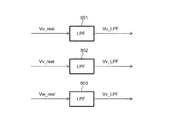
- the sixth embodiment differs from the first embodiment in output voltage detection circuits 601, 602, and 603 and an inverter failure detection unit 604.
- FIG. 18 is a block diagram showing the output voltage detection circuit shown in FIG.
- output voltage detection circuits 601, 602, and 603 are low-pass filters (LPF).
- the output voltage detection circuit 601 receives Vu_real among the three-phase voltages Vu_real, Vv_real, and Vw_real output from the inverter 3 and outputs a voltage Vu_LPF obtained by removing the carrier frequency component from Vu_real.
- the carrier frequency component is a carrier component and is the reciprocal of the carrier cycle Tc.
- the output voltage detection circuit 602 receives Vv_real among the three-phase voltages Vu_real, Vv_real, and Vw_real output from the inverter 3, and outputs a voltage Vv_LPF obtained by removing the carrier frequency component from Vv_real.
- the output voltage detection circuit 603 receives Vw_real among the three-phase voltages Vu_real, Vv_real, and Vw_real output from the inverter 3, and outputs a voltage Vw_LPF obtained by removing the carrier frequency component from Vw_real.
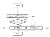
- FIG. 19 is a flowchart showing the operation of the inverter failure detection unit 604.
- are calculated based on Vv_LPF and Vw_LPF, respectively. If the difference is larger than the error reference value V_err_th, a signal for stopping the inverter 3 is output.
- the first offset voltage when the three-phase voltage command exceeds the current detection upper limit value, the first offset voltage is set so that the phase with the largest corrected three-phase voltage command matches the current detection upper limit value. Voffset1 was set. Therefore, since Vu_LPF, Vw_LPF, and Vw_LPF have values smaller than the DC voltage Vdc, it can be distinguished from a power fault.
- FIG. 20 is an overall configuration diagram showing a power conversion device according to Embodiment 7 of the present invention.
- the seventh embodiment differs from the first embodiment in an output voltage detection circuit 701 and an inverter failure detection unit 702.
- FIG. 21 is a block diagram showing the output voltage detection circuit shown in FIG.
- the output voltage detection circuit 701 includes a low-pass filter (LPF) 711.
- LPF low-pass filter
- the output voltage detection circuit 701 detects the three-phase voltages Vu_real, Vv_real, and Vw_real output from the inverter 3, adds all the phases, and removes the carrier frequency component from the addition using the low-pass filter (LPF) 711.
- the voltage Vadd_LPF is output.
- the carrier frequency component is a carrier component and is the reciprocal of the carrier cycle Tc.
- FIG. 22 is a flowchart showing the operation of the inverter failure detection unit 702.
- the amplitude value Vamp of the three-phase voltage command is calculated by the above equation (1). Subsequently, in S902, it is determined whether the amplitude value Vamp is larger than the amplitude threshold value Vthx.
- Vthx is set so that the maximum phase is equal to or less than the current detection condition value even if the three-phase voltage command is output as it is as the modified three-phase voltage command.
- FIG. 23 is an explanatory diagram showing output waveforms of the conventional power converter.
- the upper stage is a waveform of three-phase voltages Vu_real, Vv_real, and Vw_real, and two-phase modulation is performed before time t2.
- the lower row shows the waveform of Vadd_LPF.
- the left side of the modulation method switching point (t2) is a region where the amplitude value Vamp is larger than Vthx and NO is selected in the processing of S902 of FIG.
- the area on the right side of t2 is an area where the amplitude value Vamp is smaller than Vthx and YES is selected in the processing of S902 of FIG.
- Vadd_LPF is a response by the low-pass filter process shown in FIG. A delay occurs and does not instantaneously reach 1.5 Vdc at time t2, and exceeds 1.5 Vdc + Vadd_err_th in the interval from time t2 to t3.
- FIG. 24 is an explanatory diagram showing output waveforms of the power conversion device according to the seventh embodiment of the present invention.
- the upper stage shows the waveforms of the three-phase voltages Vu_real, Vv_real, and Vw_real, and has the same amplitude as the upper stage of FIG. Further, before the time t1, the maximum phase of the three-phase voltage commands Vub, Vvb, Vwb is higher than the current detection upper limit value and lower than after t1.
- the first offset when the three-phase voltage command exceeds the current detection upper limit value, the first offset is set so that the phase with the largest corrected three-phase voltage command matches the current detection upper limit value.
- the voltage Voffset1 was set. Therefore, before time t1, the variation of Vadd_LPF is also smaller than that before time t2 in FIG. 23, and is in the range of 1.5Vdc ⁇ Vadd_err_th to 1.5Vdc + Vadd_err_th.
- Vadd_LPF does not deviate from the range of 1.5Vdc ⁇ Vadd_err_th to 1.5Vdc + Vadd_err_th, and
Landscapes
- Engineering & Computer Science (AREA)
- Power Engineering (AREA)
- Physics & Mathematics (AREA)
- General Physics & Mathematics (AREA)
- Inverter Devices (AREA)
Abstract
Priority Applications (6)
| Application Number | Priority Date | Filing Date | Title |
|---|---|---|---|
| PCT/JP2016/059931 WO2017168522A1 (fr) | 2016-03-28 | 2016-03-28 | Convertisseur de puissance |
| CN201680083842.5A CN109121454B (zh) | 2016-03-28 | 2016-03-28 | 功率转换装置 |
| EP16896742.0A EP3439163B1 (fr) | 2016-03-28 | 2016-03-28 | Convertisseur de puissance |
| US16/079,176 US10411615B2 (en) | 2016-03-28 | 2016-03-28 | Power converter |
| JP2018507845A JP6525364B2 (ja) | 2016-03-28 | 2016-03-28 | 電力変換装置 |
| EP22183544.0A EP4092901A1 (fr) | 2016-03-28 | 2016-03-28 | Transformateur électrique |
Applications Claiming Priority (1)
| Application Number | Priority Date | Filing Date | Title |
|---|---|---|---|
| PCT/JP2016/059931 WO2017168522A1 (fr) | 2016-03-28 | 2016-03-28 | Convertisseur de puissance |
Publications (1)
| Publication Number | Publication Date |
|---|---|
| WO2017168522A1 true WO2017168522A1 (fr) | 2017-10-05 |
Family
ID=59963678
Family Applications (1)
| Application Number | Title | Priority Date | Filing Date |
|---|---|---|---|
| PCT/JP2016/059931 WO2017168522A1 (fr) | 2016-03-28 | 2016-03-28 | Convertisseur de puissance |
Country Status (5)
| Country | Link |
|---|---|
| US (1) | US10411615B2 (fr) |
| EP (2) | EP3439163B1 (fr) |
| JP (1) | JP6525364B2 (fr) |
| CN (1) | CN109121454B (fr) |
| WO (1) | WO2017168522A1 (fr) |
Cited By (3)
| Publication number | Priority date | Publication date | Assignee | Title |
|---|---|---|---|---|
| WO2022181084A1 (fr) * | 2021-02-25 | 2022-09-01 | 日本電産株式会社 | Circuit onduleur et module moteur |
| WO2022208911A1 (fr) * | 2021-03-30 | 2022-10-06 | 日本電産株式会社 | Dispositif de conversion de puissance et module de moteur |
| JP7471414B2 (ja) | 2020-06-16 | 2024-04-19 | 三菱電機株式会社 | 電力変換装置、及び電動パワーステアリング装置 |
Families Citing this family (4)
| Publication number | Priority date | Publication date | Assignee | Title |
|---|---|---|---|---|
| DE102020111901B3 (de) * | 2020-05-03 | 2021-04-22 | Iav Gmbh Ingenieurgesellschaft Auto Und Verkehr | Verfahren und Vorrichtung zur Bestimmung des Zwischenkreisstromes eines Stromrichters |
| EP4030611B1 (fr) * | 2020-11-17 | 2022-12-21 | Jiangsu Contemporary Amperex Technology Limited | Procédé et dispositif de commande pour onduleur connecté au réseau |
| WO2022130480A1 (fr) * | 2020-12-15 | 2022-06-23 | 三菱電機株式会社 | Dispositif de conversion de puissance |
| CN116054620A (zh) * | 2021-10-28 | 2023-05-02 | 台达电子工业股份有限公司 | 功率转换器的控制方法与功率转换器 |
Citations (2)
| Publication number | Priority date | Publication date | Assignee | Title |
|---|---|---|---|---|
| JP2005253229A (ja) * | 2004-03-05 | 2005-09-15 | Mitsubishi Electric Corp | 相電圧指令値補正方法およびこの相電圧指令値補正方法を使用したモータ制御装置 |
| JP2009189203A (ja) * | 2008-02-08 | 2009-08-20 | Denso Corp | Eps用モータ駆動装置 |
Family Cites Families (10)
| Publication number | Priority date | Publication date | Assignee | Title |
|---|---|---|---|---|
| JP2577738B2 (ja) | 1987-05-20 | 1997-02-05 | 三菱電機株式会社 | Pwmインバ−タ装置 |
| JP2006081327A (ja) * | 2004-09-10 | 2006-03-23 | Mitsubishi Electric Corp | インバータの故障検出装置 |
| JP4082438B2 (ja) * | 2006-08-30 | 2008-04-30 | ダイキン工業株式会社 | 電流制御形電力変換装置 |
| JP5122505B2 (ja) * | 2009-03-09 | 2013-01-16 | 株式会社日立産機システム | 電力変換装置及びその制御方法 |
| KR101266278B1 (ko) * | 2009-04-16 | 2013-05-22 | 메이덴샤 코포레이션 | 전력변환장치의 제어방법 |
| JP5354369B2 (ja) | 2009-09-09 | 2013-11-27 | 株式会社デンソー | 電力変換装置 |
| JP5161985B2 (ja) * | 2011-02-16 | 2013-03-13 | 三菱電機株式会社 | 電力変換装置および電動パワーステアリングの制御装置 |
| JP5831444B2 (ja) * | 2012-12-26 | 2015-12-09 | 株式会社デンソー | 回転機の制御装置 |
| US9553540B2 (en) * | 2015-01-21 | 2017-01-24 | Ford Global Technologies, Llc | Power converter with pre-compensation for dead-time insertion |
| JP2019013071A (ja) * | 2017-06-29 | 2019-01-24 | ルネサスエレクトロニクス株式会社 | 演算装置及び処理装置 |
-
2016
- 2016-03-28 JP JP2018507845A patent/JP6525364B2/ja active Active
- 2016-03-28 EP EP16896742.0A patent/EP3439163B1/fr active Active
- 2016-03-28 CN CN201680083842.5A patent/CN109121454B/zh active Active
- 2016-03-28 WO PCT/JP2016/059931 patent/WO2017168522A1/fr active Application Filing
- 2016-03-28 US US16/079,176 patent/US10411615B2/en active Active
- 2016-03-28 EP EP22183544.0A patent/EP4092901A1/fr active Pending
Patent Citations (2)
| Publication number | Priority date | Publication date | Assignee | Title |
|---|---|---|---|---|
| JP2005253229A (ja) * | 2004-03-05 | 2005-09-15 | Mitsubishi Electric Corp | 相電圧指令値補正方法およびこの相電圧指令値補正方法を使用したモータ制御装置 |
| JP2009189203A (ja) * | 2008-02-08 | 2009-08-20 | Denso Corp | Eps用モータ駆動装置 |
Non-Patent Citations (1)
| Title |
|---|
| See also references of EP3439163A4 * |
Cited By (3)
| Publication number | Priority date | Publication date | Assignee | Title |
|---|---|---|---|---|
| JP7471414B2 (ja) | 2020-06-16 | 2024-04-19 | 三菱電機株式会社 | 電力変換装置、及び電動パワーステアリング装置 |
| WO2022181084A1 (fr) * | 2021-02-25 | 2022-09-01 | 日本電産株式会社 | Circuit onduleur et module moteur |
| WO2022208911A1 (fr) * | 2021-03-30 | 2022-10-06 | 日本電産株式会社 | Dispositif de conversion de puissance et module de moteur |
Also Published As
| Publication number | Publication date |
|---|---|
| US10411615B2 (en) | 2019-09-10 |
| EP3439163A4 (fr) | 2019-06-19 |
| JPWO2017168522A1 (ja) | 2018-06-28 |
| CN109121454A (zh) | 2019-01-01 |
| JP6525364B2 (ja) | 2019-06-05 |
| EP4092901A1 (fr) | 2022-11-23 |
| CN109121454B (zh) | 2020-10-30 |
| US20190058418A1 (en) | 2019-02-21 |
| EP3439163B1 (fr) | 2022-08-31 |
| EP3439163A1 (fr) | 2019-02-06 |
Similar Documents
| Publication | Publication Date | Title |
|---|---|---|
| WO2017168522A1 (fr) | Convertisseur de puissance | |
| US8816612B2 (en) | Controller for multi-phase rotary device | |
| US8339089B2 (en) | Power converter | |
| JP5161985B2 (ja) | 電力変換装置および電動パワーステアリングの制御装置 | |
| US10374503B2 (en) | Power conversion device | |
| US11218107B2 (en) | Control device for power converter | |
| CN107438943B (zh) | 交流旋转电机的控制装置和电动助力转向系统的控制装置 | |
| JP2015208143A (ja) | 電動機駆動装置 | |
| WO2014024460A1 (fr) | Appareil de commande de moteur | |
| JP5278723B2 (ja) | モータの制御装置及びモータの制御方法 | |
| JP2006317425A (ja) | 電力変換回路の交流電圧検出方式 | |
| JP6293401B2 (ja) | 空気調和機のモータ制御装置及び空気調和機 | |
| JP6024245B2 (ja) | インバータ制御装置 | |
| US10526007B2 (en) | Power conversion device, control method for same, and electric power steering control device | |
| JP2006074951A (ja) | 交流電動機の制御装置 | |
| JP2014036539A (ja) | インバータ装置及びインバータ装置のスイッチングタイミング補正方法 | |
| JP5473071B2 (ja) | 負荷制御装置 | |
| US9935575B2 (en) | Power conversion device and control method for same, and electric power steering control device | |
| WO2022130480A1 (fr) | Dispositif de conversion de puissance | |
| JP6324615B2 (ja) | 交流回転機の制御装置および電動パワーステアリングの制御装置 | |
| CN108432124B (zh) | 电力转换装置和电力转换方法 | |
| JP6575865B2 (ja) | 3レベルインバータの制御方法及び制御装置 | |
| CN115769483A (zh) | 功率转换装置和电动助力转向装置 | |
| US20140097773A1 (en) | Method and device for operating an electronically commutated electric machine |
Legal Events
| Date | Code | Title | Description |
|---|---|---|---|
| ENP | Entry into the national phase |
Ref document number: 2018507845 Country of ref document: JP Kind code of ref document: A |
|
| NENP | Non-entry into the national phase |
Ref country code: DE |
|
| WWE | Wipo information: entry into national phase |
Ref document number: 2016896742 Country of ref document: EP |
|
| ENP | Entry into the national phase |
Ref document number: 2016896742 Country of ref document: EP Effective date: 20181029 |
|
| 121 | Ep: the epo has been informed by wipo that ep was designated in this application |
Ref document number: 16896742 Country of ref document: EP Kind code of ref document: A1 |