WO2017163440A1 - 蒸着装置、蒸着方法及び有機el表示装置の製造方法 - Google Patents
蒸着装置、蒸着方法及び有機el表示装置の製造方法 Download PDFInfo
- Publication number
- WO2017163440A1 WO2017163440A1 PCT/JP2016/071623 JP2016071623W WO2017163440A1 WO 2017163440 A1 WO2017163440 A1 WO 2017163440A1 JP 2016071623 W JP2016071623 W JP 2016071623W WO 2017163440 A1 WO2017163440 A1 WO 2017163440A1
- Authority
- WO
- WIPO (PCT)
- Prior art keywords
- vapor deposition
- substrate
- deposition mask
- mask
- deflection
- Prior art date
- Legal status (The legal status is an assumption and is not a legal conclusion. Google has not performed a legal analysis and makes no representation as to the accuracy of the status listed.)
- Ceased
Links
Images








Classifications
-
- C—CHEMISTRY; METALLURGY
- C23—COATING METALLIC MATERIAL; COATING MATERIAL WITH METALLIC MATERIAL; CHEMICAL SURFACE TREATMENT; DIFFUSION TREATMENT OF METALLIC MATERIAL; COATING BY VACUUM EVAPORATION, BY SPUTTERING, BY ION IMPLANTATION OR BY CHEMICAL VAPOUR DEPOSITION, IN GENERAL; INHIBITING CORROSION OF METALLIC MATERIAL OR INCRUSTATION IN GENERAL
- C23C—COATING METALLIC MATERIAL; COATING MATERIAL WITH METALLIC MATERIAL; SURFACE TREATMENT OF METALLIC MATERIAL BY DIFFUSION INTO THE SURFACE, BY CHEMICAL CONVERSION OR SUBSTITUTION; COATING BY VACUUM EVAPORATION, BY SPUTTERING, BY ION IMPLANTATION OR BY CHEMICAL VAPOUR DEPOSITION, IN GENERAL
- C23C14/00—Coating by vacuum evaporation, by sputtering or by ion implantation of the coating forming material
- C23C14/04—Coating on selected surface areas, e.g. using masks
- C23C14/042—Coating on selected surface areas, e.g. using masks using masks
-
- C—CHEMISTRY; METALLURGY
- C23—COATING METALLIC MATERIAL; COATING MATERIAL WITH METALLIC MATERIAL; CHEMICAL SURFACE TREATMENT; DIFFUSION TREATMENT OF METALLIC MATERIAL; COATING BY VACUUM EVAPORATION, BY SPUTTERING, BY ION IMPLANTATION OR BY CHEMICAL VAPOUR DEPOSITION, IN GENERAL; INHIBITING CORROSION OF METALLIC MATERIAL OR INCRUSTATION IN GENERAL
- C23C—COATING METALLIC MATERIAL; COATING MATERIAL WITH METALLIC MATERIAL; SURFACE TREATMENT OF METALLIC MATERIAL BY DIFFUSION INTO THE SURFACE, BY CHEMICAL CONVERSION OR SUBSTITUTION; COATING BY VACUUM EVAPORATION, BY SPUTTERING, BY ION IMPLANTATION OR BY CHEMICAL VAPOUR DEPOSITION, IN GENERAL
- C23C14/00—Coating by vacuum evaporation, by sputtering or by ion implantation of the coating forming material
- C23C14/06—Coating by vacuum evaporation, by sputtering or by ion implantation of the coating forming material characterised by the coating material
- C23C14/12—Organic material
-
- C—CHEMISTRY; METALLURGY
- C23—COATING METALLIC MATERIAL; COATING MATERIAL WITH METALLIC MATERIAL; CHEMICAL SURFACE TREATMENT; DIFFUSION TREATMENT OF METALLIC MATERIAL; COATING BY VACUUM EVAPORATION, BY SPUTTERING, BY ION IMPLANTATION OR BY CHEMICAL VAPOUR DEPOSITION, IN GENERAL; INHIBITING CORROSION OF METALLIC MATERIAL OR INCRUSTATION IN GENERAL
- C23C—COATING METALLIC MATERIAL; COATING MATERIAL WITH METALLIC MATERIAL; SURFACE TREATMENT OF METALLIC MATERIAL BY DIFFUSION INTO THE SURFACE, BY CHEMICAL CONVERSION OR SUBSTITUTION; COATING BY VACUUM EVAPORATION, BY SPUTTERING, BY ION IMPLANTATION OR BY CHEMICAL VAPOUR DEPOSITION, IN GENERAL
- C23C14/00—Coating by vacuum evaporation, by sputtering or by ion implantation of the coating forming material
- C23C14/22—Coating by vacuum evaporation, by sputtering or by ion implantation of the coating forming material characterised by the process of coating
- C23C14/50—Substrate holders
-
- H—ELECTRICITY
- H05—ELECTRIC TECHNIQUES NOT OTHERWISE PROVIDED FOR
- H05B—ELECTRIC HEATING; ELECTRIC LIGHT SOURCES NOT OTHERWISE PROVIDED FOR; CIRCUIT ARRANGEMENTS FOR ELECTRIC LIGHT SOURCES, IN GENERAL
- H05B33/00—Electroluminescent light sources
- H05B33/10—Apparatus or processes specially adapted to the manufacture of electroluminescent light sources
-
- H—ELECTRICITY
- H10—SEMICONDUCTOR DEVICES; ELECTRIC SOLID-STATE DEVICES NOT OTHERWISE PROVIDED FOR
- H10K—ORGANIC ELECTRIC SOLID-STATE DEVICES
- H10K59/00—Integrated devices, or assemblies of multiple devices, comprising at least one organic light-emitting element covered by group H10K50/00
- H10K59/10—OLED displays
- H10K59/12—Active-matrix OLED [AMOLED] displays
- H10K59/1201—Manufacture or treatment
-
- H—ELECTRICITY
- H10—SEMICONDUCTOR DEVICES; ELECTRIC SOLID-STATE DEVICES NOT OTHERWISE PROVIDED FOR
- H10K—ORGANIC ELECTRIC SOLID-STATE DEVICES
- H10K71/00—Manufacture or treatment specially adapted for the organic devices covered by this subclass
- H10K71/10—Deposition of organic active material
- H10K71/16—Deposition of organic active material using physical vapour deposition [PVD], e.g. vacuum deposition or sputtering
- H10K71/166—Deposition of organic active material using physical vapour deposition [PVD], e.g. vacuum deposition or sputtering using selective deposition, e.g. using a mask
Definitions
- the present invention relates to a vapor deposition apparatus, a vapor deposition method, and a method for manufacturing an organic EL display apparatus used when vapor-depositing an organic layer of an organic EL display apparatus. More specifically, a vapor deposition apparatus, a vapor deposition method, and an organic EL display using the vapor deposition method can reduce the blur and non-uniformity of the vapor deposition pattern by depositing the vapor deposition mask and the substrate to be vapor-deposited.
- the present invention relates to a device manufacturing method.
- the vapor deposition mask is formed of a resin film or a composite mask of a resin film and a metal support layer that can be easily processed precisely. Furthermore, the screen of the organic EL display device tends to be enlarged, or a multi-face mask that vapor deposits a plurality of panels together tends to be used from the viewpoint of production efficiency. As a result, one side of the vapor deposition mask is also 1 m or larger.
- FIG. 6 when an organic EL display device is manufactured, as shown in FIG. 6, a mask 81 is placed on a mask support base 85, a substrate 83 is placed thereon, and these are placed inside the chamber 90.
- the A vapor deposition material is scattered from a vapor deposition source 84 disposed below the mask 81, and the vapor deposition material is vapor deposited on the substrate 83 through the opening of the mask 81, thereby forming a laminated film of organic layers (see, for example, Patent Document 1). ).
- 82 is a frame for fixing the periphery of the mask 81
- 86 is a substrate support for holding the substrate 83.
- Patent Document 1 As the size of the substrate 83 and the mask 81 is increased, the central portion of the mask 81 hangs down in the vapor deposition process, resulting in a defective pattern film on the substrate 83. Provided. It is described that the substrate 83 and the mask 81 are brought into close contact with each other by pressing the flexible plate 87 of the substrate-mask contact unit 88 toward the mask 81 along the curved shape of the substrate 83.
- Patent Document 2 even when the substrate 83 and the mask 81 are increased in size, the substrate 83 is bent in order to improve the adhesion between them and improve the accuracy of the vapor deposition pattern formed on the substrate 83. It is disclosed that a substrate weighting mechanism 91 for applying a weight according to the amount at a plurality of points from the back side of the substrate 83 is disclosed. That is, as shown in FIG. 7, the substrate 83 and the mask 81 are applied with a load applied to a plurality of portions of the substrate 83 by a weighting mechanism 91 formed by a plurality of plungers 91 b screwed into the through holes of the plunger holder 91 a. It is described as adhering.
- the present invention has been made in view of such a situation.
- a vapor deposition material is vapor-deposited
- the pattern of the vapor-deposited film is not formed by forming a gap between the vapor deposition mask and the vapor deposition substrate. It is an object of the present invention to provide a vapor deposition method and a vapor deposition apparatus capable of vapor deposition with an accurate pattern so as not to be uniform.
- Another object of the present invention is to provide a method for producing an organic EL display device having excellent display quality by using the above vapor deposition method.
- a resin film is also used for a vapor deposition mask as the organic EL display device and the like become higher in definition. Further, as the deposition substrate and the vapor deposition mask become larger, the central portion of the vapor deposition mask. There is a problem that hangs down. Magnetic chuck system that uses a composite type vapor deposition mask in which a metal support layer made of a magnetic material is laminated with a resin film, and attracts the vapor deposition mask by attracting each other by a magnet provided on the opposite side of the vapor deposition mask of the substrate to be deposited Is also adopted.
- the metal support layer also needs to be thinned so that shadows are not formed during vapor deposition, and the magnetic attractive force proportional to the volume of the magnetic material also becomes weaker. Furthermore, even if the magnetic field of the magnet is increased, the vapor deposition mask becomes thin and the rigidity is weakened, so that the vapor deposition mask is deformed or wrinkled. Further, when the suction force is excessively increased, there arises a problem that the evaporation mask damages the evaporation surface of the evaporation target substrate. Therefore, a method for increasing the adsorption by magnetic force is not suitable as a solution.
- Patent Document 1 and Patent Document 2 even if the substrate to be vapor-deposited is pressed with a surface such as a flexible plate, or is applied at multiple locations with a plunger, as described above, The effective weight point is unknown, and it is considered that the deposition substrate and the deposition mask cannot be brought into close contact with each other. If there is a gap between the evaporation target substrate and the evaporation mask, the pattern of the opening of the evaporation mask cannot be transferred to the evaporation target substrate as it is. The boundaries of the image are blurred. As a result, each pattern of the organic layer laminated film formed on the deposition target substrate is not constant, and a problem of reducing display quality in a display device using the laminated film as a pixel is likely to occur.
- the present inventors performed deposition with almost no gap between the deposition mask and the deposition target substrate during deposition, thereby causing blurring of the deposited pattern and non-uniformity of the pattern.
- intensive study was repeated.
- the upper surface of the deposition substrate provided on the upper surface of the vapor deposition mask (the surface opposite to the vapor deposition mask) in the vertical direction of the central portion of the deflection of the vapor deposition mask (where the displacement from the flat state is almost the largest). It was found that the substrate to be deposited and the deposition mask can be deposited in close contact with each other during the deposition by pushing down the deposition substrate so that the deposition substrate has substantially the same deflection as that of the deposition mask.
- the substrate to be vapor-deposited is rigid such as thick glass, the substrate to be vapor-deposited becomes a curved surface even if it is pushed in a point shape at the center, and it is easy to adhere to the vapor deposition mask.
- the deposition target substrate does not necessarily have a curved surface from the center of deflection toward the fulcrum of the peripheral edge.
- it is preferable that at least the contact portion of the pressing tool that presses the deposition target substrate is in an arc shape with a radius of curvature when the center portion is pushed. By doing so, a to-be-deposited substrate and a vapor deposition mask can be stuck almost over the whole surface. This is because the deflection of the vapor deposition mask can be regarded as a substantially spherical surface.
- the amount of deflection of the vapor deposition mask may include the amount of elongation of the vapor deposition mask due to an increase in temperature during vapor deposition in addition to the length of the vapor deposition mask in the bent state due to the deflection around the periphery of the vapor deposition mask. preferable. That is, the amount of push-in is determined from the length of the vapor deposition mask in consideration of thermal expansion, and the radius of curvature of the spherical surface of the pressing tool that contacts the deposition target substrate is determined.
- a curve in a cross section cut in a direction along one side of the vapor deposition mask passing through the central portion of the vapor deposition mask is bent, and the center of the deflection is the apex.
- the length of the isosceles side can be approximated as the total length after the evaporation mask is bent.
- the deflection of the active area may be eliminated by collecting the deflections of the number of active areas (n) and pressing them down at the center of the deposition mask, or at the center of each active area.
- the total amount of the deflection amount of the entire deposition mask and the deflection amount of each active region at the place can be weighted. This point will also be described in detail later.
- the vapor deposition mask is held at the peripheral portion and disposed in the horizontal direction, a vapor deposition substrate on which the vapor deposition film is formed is disposed on the upper surface side of the vapor deposition mask, and vapor deposition is performed below the vapor deposition mask.
- a vapor deposition material is vaporized from the vapor deposition source and a vapor deposition film is formed on the vapor deposition substrate, the vertical direction of the center of deflection of the vapor deposition mask and the position of the upper surface of the vapor deposition substrate are disposed.
- a vapor deposition apparatus of the present invention includes a mask holder for placing a vapor deposition mask, a substrate holder provided so as to hold a vapor deposition substrate, and a touch plate provided in contact with the vapor deposition substrate held by the substrate holder.
- a vapor deposition source provided on the opposite side of the vapor deposition mask placed on the mask holder to vaporize vapor deposition material; and a pressure device that presses the upper surface of the vapor deposition substrate.
- it is provided so that it can be pressed at the position of the upper surface of the evaporation target substrate held by the substrate holder on the vertical line of the center part of the deflection of the evaporation mask.
- the method of manufacturing an organic EL display device includes a method of manufacturing an organic EL display device by laminating an organic layer on a device substrate, on the device substrate on which at least a TFT and a first electrode are formed on a support substrate. It includes forming a laminated film of an organic layer by vapor-depositing an organic material on the first electrode using the vapor deposition method, and forming a second electrode on the laminated film.
- the vapor deposition method of the present invention since pressing is performed on the upper surface of the substrate to be deposited on the center line due to the deflection of the vapor deposition mask, there is at least a pressing point at the position of the maximum point of deflection, and the pressing force is concentrated and predetermined. Easy to push only the amount of. Therefore, even if the deposition target substrate is a glass plate, it is easy to push only a predetermined amount. Rather, if the substrate to be deposited is glass, it has rigidity, so even if it is pressed at a point, only that point is not recessed but it is pushed in with a smooth curved surface.
- the deposition target substrate is recessed with a concave curved surface where the pushed point is the apex.
- the pressing force works effectively, a concave curved surface similar to the deflection of the vapor deposition mask is obtained, and the adhesion with the vapor deposition mask is very excellent.
- the substrate to be deposited is a thin glass plate or a flexible substrate made of a resin film
- the rigidity is small, the surface of the pressing tool that contacts the substrate to be deposited is in a state where the deposition mask is bent.
- the curved surface has a curvature radius at that time, the point where the force is applied is mainly the central portion of the deflection, but the substrate to be deposited is deformed along the shape of the pressing tool also around it. Even in the case of the above-described rigid glass plate, it is preferable to make the tip shape a curved surface rather than pressing with a sharp stick or a tip with a flat tip.
- the curved surface at the tip is preferably combined with the curved surface due to the deflection of the vapor deposition mask.
- the pressing device is provided so as to be able to press at the position of the upper surface of the vapor deposition substrate held by the substrate holder on the vertical line of the center portion of the vapor deposition mask. Pushing by a predetermined amount is very easy.
- a plunger preferably having a curved surface as described above
- a predetermined amount may be provided between the touch plate and a deposition target substrate held by the substrate holder.
- a pressing tool having a curved surface such as a sphere or a pressing tool having a spherical surface in a wide range in contact with the deposition target substrate at a predetermined position.
- the deposition target substrate can be pushed down by a predetermined amount very easily.
- the laminated film of the organic layer does not blur or become non-uniform in size, so that a very clear pixel can be obtained. As a result, an organic EL display device with very excellent display quality can be obtained.
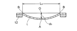
- FIG. 2 is a diagram for explaining deflection of the vapor deposition mask of FIGS. 1A to 1B.
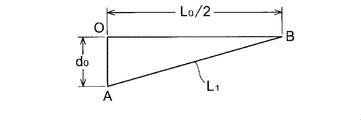
- FIG. 1B is an explanatory diagram for obtaining the length of a vapor deposition mask in a bent state of the vapor deposition mask of FIGS. 1A to 1B.
- planar explanatory drawing plane explanatory drawing (planar explanatory drawing which removed the to-be-deposited board
- FIG. 3A on a vapor deposition mask. It is the schematic of an example which calculates the pushing amount of FIG. 4A. It is a figure which shows the example of a shape of a pressing tool when adhere
- the vapor deposition mask 1 is held in the frame 12 at the peripheral portion and arranged in the horizontal direction, and the vapor deposition substrate 2 on which the vapor deposition film is formed on the upper surface (upper vertical direction) side of the vapor deposition mask 1 They are placed one on top of the other.
- a vapor deposition source 5 is disposed below the vapor deposition mask 1, and a vapor deposition material 51 is vaporized from the vapor deposition source 5, whereby a vapor deposition film is formed on the vapor deposition substrate 2.
- the depth of the deflection with the peripheral edge of the deposition mask 1 as a fulcrum or an amount exceeding the depth The deposition substrate 2 is pushed in and deposited while the deposition target substrate 2 and the deposition mask 1 are brought into close contact with each other.
- the length of the arc connecting the fulcrum (point B in FIG. 2A) which is the peripheral portion of the vapor deposition mask 1 and the center of deflection of the vapor deposition mask 1 (point A in FIG. 2A), and the object in contact with the position of the fulcrum.
- the position of the vapor deposition substrate 2 on the vapor deposition mask 1 side and the length of the arc of the vapor deposition substrate that connects the position of the surface on the vapor deposition mask 1 side of the vapor deposition substrate 2 that intersects the vertical line of the center of deflection are substantially equal.
- the deposition target substrate 2 is pushed in.
- the deposition substrate 2 is pushed in so that the curvature radii of the surfaces where the deposition mask 1 and the deposition substrate 2 are in contact with each other are substantially equal.
- the depth of deflection of the vapor deposition mask 1 or the pushing of an amount exceeding the depth is referred to as an active region 14 described later (see FIGS. 3A and 3B) in addition to the deflection with the peripheral edge of the vapor deposition mask 1 as a fulcrum. This is because there is also a need to compensate for the deflection of the vapor deposition mask accompanying elongation due to thermal expansion during vapor deposition.
- Compensating for thermal expansion means that the dimensions are not changed from the pre-stretched state even by thermal expansion by extending in advance by the amount expanded by heat.
- thermal expansion is compensated.
- the actual pushing amount may be twice or more and 10 times or less, more preferably 3 times or more and about 7 times or less of the bending with the peripheral edge as a fulcrum. That is, it is preferable to push in an amount exceeding the depth of bending with the peripheral edge as a fulcrum.
- an arrow line on the upper side of the deposition target substrate 2 indicates a position where a load for pushing the deposition target substrate 2 is applied.
- the pressing device 3 for pressing the deposition target substrate 2 includes a pressing tool 30 formed of a rigid sphere 31 such as a steel ball or a rigid plastic sphere from a touch plate 41 and an actuator (not shown).
- a pressing tool 30 formed of a rigid sphere 31 such as a steel ball or a rigid plastic sphere from a touch plate 41 and an actuator (not shown).
- the pressing device 3 is not limited to this example, and the plunger may be pressed by a certain amount by an actuator or the like.
- the shape of the tip of the plunger is preferably a curved surface, more preferably a spherical surface with a radius of curvature of the curved surface of the vapor deposition mask 1.
- the pressing tool 30 may not be the sphere 31 but may be a pressing tool 30 having an appropriate shape.
- a spherical notch 32 in which a part of a sphere is cut out may be formed by forming a surface of the pressing tool 30 that contacts the deposition target substrate 2 into a spherical surface having a curvature radius of the curved surface of the deposition mask 1. .
- the main push-in is at the center of the bend, but the push-in force works around it, and the deposition target substrate 2 can be pushed in with a spherical surface. Even in this case, there is no difference from pressing in the central part of the deflection.
- the area around the center is auxiliary, and the total force does not change just by distributing the force pushing the center to the surface.
- a spherical part 33 with a convex part in which a convex part is formed on the spherical part may be used.
- variety made into a spherical surface (length fitted in the touch plate 41 of FIG. 1B) will not be specifically limited if it is less than the inner dimension of a flame
- the leg portions 32a and 33a are formed on the ball missing bodies 32 and 33 in order to be fitted to the touch plate 41, but they may be omitted.
- the spheres 32 and 33 without the legs 32a and 33a may be attached to the touch plate 41, or the spheres 32 and 33 without the legs 32a and 33a are integrated with the touch plate 41 and the like. May be formed.
- the spherical surface of the portion of the pressing tool 30 that comes into contact with the deposition target substrate 2 is preferably a curved surface of the deposition mask 1, specifically, a spherical surface having a radius of curvature of a portion corresponding to the depth of deflection. Will be described later.
- the spherical surface of the portion of the pressing tool 30 that comes into contact with the deposition target substrate 2 has a radius of curvature determined from the curved surface of the deposition mask 1 in a bent state. It is characterized by being spherical.
- the length of the vapor deposition mask 1 or the substrate 2 to be vapor-deposited means the length in one direction in a cross section cut in a direction parallel to one side of the vapor deposition mask 1 through the center of the deflection of the vapor deposition mask 1.
- the cross section of the vapor deposition mask 1 and the vapor deposition substrate 2 due to the bending is curved, but the lengths thereof are as shown in FIGS. 2A to 2B. ) It can be approximated by the sum of two isosceles triangles connecting B (only half is shown in FIG. 2B). In other words, when considered in half, the right-sided triangle OAB has a hypotenuse length AB (see FIG.
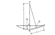
- the radius of curvature r of the vapor deposition mask 1 in the bent state is assumed to be a circular arc of the line segment AB (midpoint is G), assuming that the cross-sectional shape of the bending is an arc.
- the intersection F of the extension line of the deflection OA becomes the center point of the deflection curve, and thus can be obtained by obtaining the length r of the line segment FA.
- the amount of sagging deflection (the distance at which the central portion sags) d 0 (see FIG. 2A) with the peripheral edge of the vapor deposition mask 1 as a fulcrum can be measured optically.
- the length of the vapor deposition mask 1 when the vapor deposition mask 1 is bent is approximated by 2L 1 (see FIG. 2B).
- L 1 ⁇ d 0 2 + (L 0/2) 2 ⁇ 1/2 ⁇ (1) It is. That is, as shown in FIG.
- the vapor deposition mask 1 when the vapor deposition mask 1 is simply bent with the peripheral edge of the vapor deposition mask 1 as a fulcrum, by pushing the vapor deposition substrate 2 by the deflection amount d 0 of the vapor deposition mask 1,
- the length of the vapor deposition mask 1 after the vapor deposition mask 1 is bent is substantially equal to the length after the deposition substrate 2 is pushed.
- the deflection is exaggerated, but the actual deflection d 0 is, for example, about 700 ⁇ m with a 700 mm ⁇ 450 mm evaporation mask.
- the radius of curvature r at the center of the bending at this time is expressed as ⁇ AGF, with reference to FIG. 2C, where G is the middle point of the line segment AB and F is the center point when the shape of the bending is a sphere.
- the bending depth is d. Accordingly, when the deflection shown in FIG. 1B to be described later is d, L 1 is also different as will be described later, but the surface of the pressing tool 30 that contacts the deposition target substrate 2 is d and L at that time. It is preferable to use a spherical surface with a curvature radius r determined by 1 .
- the vapor deposition material is vaporized from the vapor deposition source 5 and vapor deposition is performed as described above. Therefore, the temperature of the vapor deposition source 5 is high and the temperature of the vapor deposition mask 1 is also increased. If the temperature of the vapor deposition mask 1 rises, the deflection will increase accordingly. The amount of deflection due to this thermal expansion is being deposited and cannot be measured directly. However, the elongation of the vapor deposition mask 1 itself is, for example, if the linear expansion coefficient of the vapor deposition mask 1 is ⁇ and the temperature rise is t, the thermal expansion amount of the vapor deposition mask 1 is ⁇ tL 1 .
- the half length of the vapor deposition mask 1 is L 1 due to the deflection due to the horizontal arrangement described above
- the vapor deposition mask 1 is pushed and deformed (stretched), but because the vapor deposition mask 1 is distorted by that amount. Then, when the temperature rises and the vapor deposition mask 1 extends, the expansion due to the thermal expansion eliminates the distortion of the vapor deposition mask 1, and just the expansion of the vapor deposition mask 1 due to the thermal expansion and the pushing of d 2 of the deposition substrate 2. The amount is matched, and the deposition substrate 2 and the deposition mask 1 are in close contact with each other.
- the elongation due to the coefficient of thermal expansion is less than 1 ⁇ m if the temperature rise during vapor deposition of the vapor deposition mask 1 is about 1 ° C. However, considering the case where the temperature rises, the effect of d 2 becomes remarkable. .
- the indentation amount of d 2 and the elongation due to thermal expansion of the vapor deposition mask 1 are matched, and the vapor deposition substrate 2 and the vapor deposition mask 1 are in close contact with each other.
- the above example is an example of the vapor deposition mask 1 which is uniform as a whole, but there may be a multi-sided vapor deposition mask in which a plurality of relatively small panels such as a smart phone are vapor deposited together.
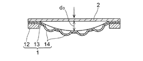
- an example of such a vapor deposition mask 1 is that an active region 14 is formed in the opening of the metal film 13, and a fine opening corresponding to the vapor deposition pattern is formed in the active region 14. Part is formed.
- the active region 14 may be entirely made of a resin film, or may be formed of a composite mask of a resin film and a metal support layer.
- the rigidity is weaker than that of the portion of the metal film 13, so that the metal film 13 is easily bent.
- FIG. 3B the deflection of the original vapor deposition mask 1 as a whole (deflection using the peripheral edge as a fulcrum) is shown in an exaggerated manner by showing a cross section cut along one side of the vapor deposition mask 1 through the center of the deflection. )
- d the inventors have found that there is a deflection h 0 (see FIG. 3C) of each active region 14.
- the deposition substrate 2 and the deposition mask 1 cannot be brought into close contact with each other unless the deposition substrate 2 is stretched even in the portion where the length of the deposition mask 1 changes due to the deflection h 0 in the active region 14. They found out.
- the bending state of one active region 14 is simply shown by a cross-sectional view passing through the central portion of the bending along one side of the above-described deposition mask 1. Also in this example, as in the case described above, the length s 1 which is half the length of the active region 14 in a state where the active region 14 is bent due to bending is approximated by the length of the hypotenuse of the right triangle PQR.
- the deflection h 0 of each active region 14 can also be known by actual measurement.
- the vapor deposition mask 1 is stretched to form a clean concave surface, and the vapor deposition substrate 2 is pressed into the same concave surface by pushing the center thereof to cover the entire surface.
- the idea is that the vapor deposition substrate 2 and the vapor deposition mask 1 are brought into close contact with each other.
- the evaporation L in consideration of the length L 3 of the hypotenuse of the right-angle triangle OCD, that is, the change ⁇ s of the length of the active region 14 of the evaporation mask 1. If the length of the mask 1 is obtained, the pushing amount d 1 of the deposition target substrate 2 can be obtained.
- the arc length L 3 taking into account the deflection of the vapor deposition mask 1 is approximated by the length of the hypotenuse of the triangle OCD. Can be approximated to a triangle O′C′D ′. Therefore, the pushing amount d 1 of the deposition target substrate 2 is the depth of deflection (OC length) after adding the deflection of the active region 14 to the length of the deposition mask 1 by the deflection with the peripheral edge of the deposition mask 1 as a fulcrum. is the) coincides with the d 1.
- the vapor deposition mask 1 is in close contact.
- L 2 in equation (3) may be used instead of L 1 in equation (5) described above.
- the second method is to press the upper surface of the deposition target substrate 2 on the vertical line at the center of the deflection of each active region 14 to thereby deposit the deposition target substrate 2 in each active region 14.
- the vapor deposition mask 1 it is an image that the deposition target substrate 2 is also deflected in accordance with the deflection of the active region 14 of the deposition mask 1.
- the pushing amount d 3 of each active region 14 is, for example, as shown in FIG. 4B, a central portion of the deflection with the peripheral portion of the vapor deposition mask 1 as a fulcrum, as shown in FIG. 4B.
- the deflection of the entire deposition mask 1 x / (L 0/2) times the min d 0, i.e. 2d 0 x / and L 0, the amount plus the amount of deflection h 0 of one of the active region 14, i.e. d 3 (x) 2d 0 x / L 0 + h 0
- the substrate 2 and the vapor deposition mask 1 can be brought into close contact with each other also by pushing in.
- d x is obtained by dividing the depth d 0 due to the entire bending with the peripheral edge of the vapor deposition mask 1 as a fulcrum according to the position of each active region 14x, and the bending of the active region 14 itself. Is equal to h 0 in each active region.
- the deposition target substrate 2 is rigid like glass, there is an influence of the pressing of the adjacent active region, so that each active region 14 is adjusted so that the pressing amount is obtained while measuring the actual pressing amount. Is pressed.
- an arrow line on the upper side of the deposition target substrate 2 indicates a position where a load for pushing the deposition target substrate 2 is applied.
- each plunger is preferably a rounded curved surface.
- the deposition target substrate is a flexible substrate, if the tip of the plunger is sharp, the deposition target substrate 2 is easily broken, and even if the deposition target substrate 2 is glass, the tip of the plunger is sharp. This is because it is easy to break.
- the tip of the plunger is preferably a spherical surface corresponding to the radius of curvature of the deflection of the active region 14, and moreover, the pressure that makes such a spherical surface over almost the entire surface.
- a tool 30 (see FIG. 4C) is preferably used.
- the body 33 can be used. By using such a spherical body 33 with projections, the vapor deposition mask 1 and the vapor deposition substrate 2 can be completely adhered to each other, particularly when the vapor deposition substrate 2 is a flexible substrate.
- the radius of curvature of the spherical notch 33b is formed by the radius r according to the above-described equation (2) or the radius of curvature when using L 2 when further taking into account thermal expansion, and the radius of curvature of the convex portion 33c. Is formed by the radius of curvature calculated from FIG. 3C in the same manner as FIG. 2C described above.
- the leg portion 33a is shown, but the ball notch portion 33b without the leg portion 33a is formed integrally with the touch plate 41 (see FIG. 1B), or is bonded or overlapped. Also good.
- the vapor deposition apparatus of the present invention is held by a mask holder 15 on which the vapor deposition mask 1 is placed, a substrate holder 29 provided so as to hold the substrate 2 to be deposited, and a substrate holder 29.
- the vapor deposition material is vaporized by being provided on the opposite side of the substrate holder 29 of the vapor deposition mask 1 placed on the mask substrate 15 and the touch plate 41 provided on the vapor deposition substrate 2 in contact with the periphery of the vapor deposition substrate 2.
- a vapor deposition source 5 and a pressing device 3 that presses the upper surface of the deposition target substrate 2 are provided.
- the pressing device 3 is provided on the upper surface of the deposition substrate 2 held by the substrate holder 29 on the vertical line at the center of the deflection of the deposition mask 1 (the entire deflection of the deposition mask 1 or the individual deflection of the active region 14). It is provided so that it can be pressed at the position.
- the pressing device 3 is shown as an example of being pressed by the pressing tool 30 using the touch plate 41, but is not limited thereto. Other examples are described below.
- the pressing device 3 is formed so as to push the deposition target substrate 2 by an amount of d 0 or more and d 2 or less, or d 3 (x).
- the pressing device 3 can be composed of a pressing tool 30 made of various rigid bodies such as metal and rigid plastic, and a pressing means such as a touch plate 41 and an actuator.
- various pushing devices such as a plunger and an actuator can be used. In short, it is characterized in that it is formed so that a predetermined amount of pushing is performed at the center of any of the deflections. In addition, it is still more preferable if it is the structure contact
- FIGS. 1B and 4C This example is shown in FIGS. 1B and 4C. That is, in the example shown in FIG. 1B, a spherical notch 32 having a shape following the bending with the peripheral edge of the vapor deposition mask 1 similar to that in FIG. 1A as a fulcrum is inserted between the touch plate 41 and the vapor deposition substrate 2. ing. Except for the shape of the pressing tool 30, the structure is the same as that shown in FIG. 1A, and the same portions are denoted by the same reference numerals and description thereof is omitted.
- a part (the leg portion 32a) of the spherical missing body 32 is formed so as to be fitted into the touch plate 41, but it may be adhered to the touch plate 41 without being fitted, or the touch plate 41 may be formed integrally.
- the height of the portion protruding from the touch plate 41 may be a predetermined amount d. Also in this example, the pushing amount at the center part of the bending becomes a predetermined dimension d.
- the radius of curvature r in the case of the deflection d 0 with the peripheral edge of the vapor deposition mask 1 as a fulcrum is shown.
- the deposition substrate 2 and the deposition mask 1 can be brought into close contact with each other.
- the radius of curvature of the spherical surface of the convex portion 33c of the active region 14 is also obtained from FIG. 3C as described above.
- the substrate holder 29 is connected to a driving device (not shown) so that the peripheral portion of the deposition target substrate 2 is held by a plurality of hook-shaped arms and can be moved up and down.
- the deposition substrate 2 carried into the deposition apparatus by the robot arm is received by the hook-shaped arm, and the substrate holder 29 is lowered until the deposition substrate 2 comes close to the deposition mask 1.
- An imaging device (not shown) is also provided so that alignment can be performed.
- the touch plate 41 is supported by a support frame 42, and in the example shown in FIG.
- the touch plate 41 is pushed down until it comes into contact with the peripheral edge of the deposition substrate 2 with the sphere (pressing tool) 31 interposed therebetween, whereby the deposition substrate 2 Can be adhered to the vapor deposition mask 1.
- the pressing means including the actuator is also provided although not shown.
- the touch plate 41 is originally provided to flatten the deposition target substrate 2 and is formed of a rigid plate material. Therefore, even if the pressing tool 30 such as a sphere 31 made of a steel ball as shown in FIG. 1A is pressed, the touch plate 41 is not deformed, and is pressed down in parallel to be brought into close contact with the peripheral portion of the deposition target substrate 2. The deposition target substrate 2 is deformed.
- the sphere 31 has a height at which the distance between the touch plate 41 and the deposition target substrate 2 is a predetermined pushing amount d.
- the diameter of the sphere 31 is formed larger than a predetermined dimension d and is exposed from the touch plate 41.
- the length of the portion to be formed is formed to be a predetermined dimension d.
- the pressing device 3 may be configured to be pushed down by a plunger and an actuator instead of such a configuration.
- the touch plate 41 is rigid as described above, and even if the touch plate 41 is pressed, the touch plate 41 is pressed on a flat surface, and the pressure is dispersed so that the deposition target substrate 2 cannot be pressed at the center of the deflection. It is. In short, it is necessary that the deposition target substrate 2 be pressed at the center of the deflection.
- the touch plate 41 can also have a function of cooling the deposition target substrate 2 and the deposition mask 1 by circulating cooling water therein. Even if the pressing device 3 does not have the pressing tool 30 as in this example, the portion of the touch plate 41 that contacts the deposition target substrate 2 is the portion of the pressing tool 30 that contacts the deposition target substrate 2. Any curved surface having a shape and a height of a predetermined dimension d may be used.
- the deposition target substrate 2 and the deposition mask 1 are aligned.
- the deposition target substrate 2 is moved relative to the deposition mask 1 while imaging the alignment marks formed on the deposition mask 1 and the deposition target substrate 2 respectively. Therefore, although not shown in the drawing, an image pickup apparatus that picks up an alignment mark and a fine movement apparatus that finely moves the deposition target substrate 2 are also provided. Further, although not shown in FIG. 1A, the entirety is also provided with a vacuum device that is placed in a chamber and evacuates the chamber.
- Examples of the vapor deposition mask 1 include those formed only of a resin film, a hybrid type in which a resin film and a metal support layer are laminated, and a multi-face mask formed by collecting a plurality of panels. It can be applied to various deposition masks such as a metal mask.
- the resin film preferably has a small difference in linear expansion coefficient from the vapor deposition substrate 2, but is not particularly limited.
- polyimide (PI) resin polyethylene naphthalate (PEN) resin, polyethylene terephthalate (PET) resin, cycloolefin polymer (COP) resin, cyclic olefin copolymer (COC) resin, polycarbonate (PC) resin, polyamide resin, polyamideimide resin , Polyester resin, polyethylene resin, polyvinyl alcohol resin, polypropylene resin, polystyrene resin, polyacrylonitrile resin, ethylene vinyl acetate copolymer resin, ethylene-vinyl alcohol copolymer resin, ethylene-methacrylic acid copolymer resin, polyvinyl chloride resin, polyvinylidene chloride resin Cellophane, ionomer resin and the like can be used.
- PI polyimide
- PEN polyethylene naphthalate
- PET polyethylene terephthalate
- COP
- Polyimide resin is preferable because a linear expansion coefficient can be adjusted by conditions such as a temperature rise profile during the heat treatment when a precursor solution is applied and a heat treatment is performed to form a resin film.
- the thickness of the resin film is about several ⁇ m to several tens of ⁇ m, for example, about 5 ⁇ m or more and about 10 ⁇ m or less.
- the metal support layer When the metal support layer is formed, by using a magnetic material, magnetic adsorption can be performed by a magnet provided on the opposite side of the vapor deposition mask 1 of the vapor deposition substrate 2 (not shown), but the present invention is not limited to this.
- this metal support layer When this metal support layer is provided, an opening that is slightly larger than the opening formed in the resin film is formed in the metal support layer.
- the thickness of the metal support layer is 5 ⁇ m or more and about 30 ⁇ m or less.
- an active region 14 corresponding to each panel is formed in the metal layer 13.
- the active region 14 is made of only a resin film, and an opening may be formed, or a metal support layer may be formed around the opening in the active region 14.
- the metal support layer and the metal layer may be the same, or an active region 14 formed separately may be attached to the opening of the metal layer 13.
- the metal layer 13 preferably has a small difference in linear expansion coefficient from the deposition target substrate 2, and invar (an alloy of Fe and Ni) is particularly preferable because it hardly expands due to heat.
- the evaporation mask 1 has been enlarged in recent years, and has become a large one with a side exceeding 1 m. Moreover, whether it is a resin film or a metal support layer or a metal layer 13, it is a very thin film. Therefore, even if the periphery of the vapor deposition mask 1 is fixed by the frame 12, as shown in FIG. When held horizontally at the part, deflection occurs. In order to prevent such bending, a mask material such as a resin film is attached to the frame 12 with tension (strung) from four directions of the mask material before being attached to the frame.
- the deposition target substrate 2 is made to follow the deflection of the deposition mask 1.
- the deflection of the vapor deposition mask 1 can include not only the deflection due to its own weight but also the deflection due to thermal expansion.
- various deformations such as that the active region 14 is particularly likely to be bent based on the difference in the rigidity of the material. There is also a problem.
- the present inventors have found that it is not always necessary to push the deposition target substrate 2 by the amount of deflection of the deposition mask 1. As described above, the deposition substrate 2 and the deposition mask 1 are brought into close contact with each other by pressing the deposition substrate 2 on the central axis of the deflection of the deposition mask 1 in consideration of various deflections of the deposition mask 1. The present inventors have found that this can be achieved.
- invar having a small thermal expansion is used for the frame 12. Moreover, since it is not a thin film like a resin film or a metal support layer but is as thick as 25 mm or more and about 50 mm or less, it is strong against bending and heat. Therefore, bending occurs exclusively in the resin film and the metal support layer (metal layer 13). Since this bend is curved, it is almost close to an arc.
- a flexible substrate made of a glass substrate or a resin film is used as the deposition substrate 2. In the case of glass, since it is difficult to deform every minute, even if it is pressed at one point, it tends to be curved.
- the actual (curved) deposition mask 1 is approximated by the length of the hypotenuse of the right triangle, but the shape of the deposition substrate 2 is the same. The error is very small. Even if the deposition target substrate 2 is a flexible substrate, if the pressed portion has an arc shape corresponding to the arc shape of the deposition mask 1, it tends to have the same curved shape. Therefore, if the vapor deposition mask 1 is only bent by its own weight with the peripheral edge as a fulcrum, as shown in FIG.
- the vapor deposition mask 1 is viewed from the upper surface of the vapor deposition substrate 2 in the vertical direction with respect to the central portion of the vapor deposition mask 1.
- the vapor deposition mask 1 and the vapor deposition substrate 2 are likely to adhere to each other along the same curve (curved surface).
- the vapor deposition source 5 may be a variety of vapor deposition sources such as dotted, linear, and planar.
- a linear type vapor deposition source 5 in which crucibles are arranged in a line (in a direction perpendicular to the paper surface of FIG. 1A). Evaporation is performed on the entire surface by operating a so-called linear source, for example, from the left end to the right end of the page.
- the vapor deposition source 5 emits the vapor deposition material in such a manner that the side edges of the cross-sectional shape of the radiation beam of the vapor deposition material determined by the shape of the crucible have a cross-sectional fan shape having a certain angle.
- the vicinity of the opening of the vapor deposition mask 1 is tapered so that it reaches the predetermined location of the vapor deposition substrate 2 without being blocked by the vapor deposition mask 1. Is formed.
- the organic EL display device is manufactured by the above-described method on a device substrate 21 in which a TFT, a planarizing film, and a first electrode (for example, anode) 22 (not shown) are formed on a support substrate (not shown).
- the vapor deposition mask 1 is aligned and overlapped, and the organic material 51 is vapor-deposited to form a laminated film 25 of organic layers.
- the second electrode 26 (cathode) is formed on the laminated film 25.
- a switch element such as a TFT is formed for each RGB sub-pixel of each pixel on a support substrate such as a glass plate
- the first electrode 22 connected to the switch element includes: On the planarizing film, it is formed by a combination of a metal film such as Ag or APC and an ITO film.
- insulating banks 23 made of SiO 2, acrylic resin, polyimide resin, or the like are formed between the sub-pixels.
- the vapor deposition mask 1 is aligned and fixed on the insulating bank 23 of the device substrate 21.
- this fixing is performed, for example, by adsorbing with a magnet or the like provided on the opposite side of the vapor deposition surface of the device substrate 21 as described above.
- a magnet or the like provided on the opposite side of the vapor deposition surface of the device substrate 21 as described above.
- the organic material 51 is emitted from the vapor deposition source (crucible) 5 in the vapor deposition apparatus, and the organic material 51 is formed on the device substrate 21 only on the opening 11 a of the vapor deposition mask 1. Is deposited, and a laminated film 25 of an organic layer is formed on the first electrode 22 of the desired subpixel. Since the opening 11 a of the vapor deposition mask 1 is formed smaller than the interval between the surfaces of the insulating bank 23, the organic material 51 is hardly deposited on the side wall of the insulating bank 23. As a result, as shown in FIGS. 5A to 5B, the organic layer laminated film 25 is deposited almost only on the first electrode 22.
- This vapor deposition process is sequentially performed on each sub-pixel by changing the vapor deposition mask 1.
- a vapor deposition mask in which the same material is vapor-deposited on a plurality of subpixels at the same time is used. According to the present invention, since the vapor deposition mask 1 is in close contact with the insulating bank 23 of the device substrate 21, a very accurate organic layer laminated film 25 can be obtained.
- the organic layer laminated film 25 is simply shown as one layer, but actually, the organic layer laminated film 25 is formed of a plurality of laminated films made of different materials.
- a hole injection layer made of a material with good ionization energy consistency that improves hole injection may be provided.
- a hole transport layer capable of improving the stable transport of holes and confining electrons (energy barrier) in the light emitting layer is formed of, for example, an amine material.
- a light emitting layer selected on the basis of the light emission wavelength is formed by doping Alq 3 with red or green organic fluorescent material for red, green, for example.
- a DSA organic material As the blue material, a DSA organic material is used. On the light emitting layer, an electron transport layer that further improves the electron injection property and stably transports electrons is formed of Alq 3 or the like. By laminating each of these layers by several tens of nanometers, an organic layer laminated film 25 is formed. An electron injection layer that improves electron injection properties such as LiF and Liq may be provided between the organic layer and the metal electrode.
- an organic layer made of a material corresponding to each color of RGB is deposited on the light emitting layer.
- the hole transport layer, the electron transport layer, and the like are preferably deposited separately using a material suitable for the light emitting layer if the light emitting performance is important.
- two or three colors of RGB are laminated with the same material.
- an evaporation mask in which an opening is formed in the common subpixel is formed.
- each of the organic layers can be vapor-deposited continuously using one vapor deposition mask 1 for the R sub-pixel, or a common organic layer for RGB is deposited.
- the organic layer of each sub-pixel is vapor-deposited up to the lower side of the common layer, and the vapor-deposition mask 1 in which RGB openings are formed at the common organic layer is used for all pixels at once. An organic layer is deposited.
- the deposition mask 1 is separated, and the second electrode (for example, cathode) 26 is formed on the entire surface.
- the second electrode 26 is formed of a translucent material, for example, a thin Mg—Ag eutectic film. .
- Al or the like can be used.
- ITO, In 3 O 4 or the like is used for the first electrode 22, and the second electrode 26 is a metal having a small work function, for example, Mg, K, Li, Al, etc. can be used.
- a protective film 27 made of, for example, Si 3 N 4 is formed on the surface of the second electrode 26.
- the entirety is sealed by a sealing layer made of glass, resin film, or the like (not shown), and the organic layer laminated film 25 is configured not to absorb moisture. Further, the organic layer can be made as common as possible, and a color filter can be provided on the surface side.
- This vapor deposition mask 1 can be used repeatedly.
Landscapes
- Chemical & Material Sciences (AREA)
- Engineering & Computer Science (AREA)
- Chemical Kinetics & Catalysis (AREA)
- Materials Engineering (AREA)
- Mechanical Engineering (AREA)
- Metallurgy (AREA)
- Organic Chemistry (AREA)
- Manufacturing & Machinery (AREA)
- Microelectronics & Electronic Packaging (AREA)
- Electroluminescent Light Sources (AREA)
- Devices For Indicating Variable Information By Combining Individual Elements (AREA)
- Physical Vapour Deposition (AREA)
Abstract
蒸着材料を蒸着する際に、蒸着マスクと被蒸着基板との間にギャップが形成されることにより蒸着された膜のパターンが不均一にならないで、正確なパターンで蒸着することができる蒸着方法及びその蒸着装置を提供する。蒸着マスク(1)を周縁部でフレーム(12)に保持して水平方向に配置し、その蒸着マスク(1)の上面側に蒸着膜を形成する被蒸着基板(2)を重ねて配置し、蒸着マスク(1)の下方に蒸着源(5)を配置し、蒸着源(5)から蒸着材料(51)を気化させることにより、被蒸着基板(2)に蒸着膜が形成される。蒸着マスク(1)の撓みの中心部の鉛直方向で、被蒸着基板(2)の上面の位置から、蒸着マスク(1)の撓みによる伸び後の蒸着マスク(1)の長さ(蒸着マスクの一辺に沿った断面での長さ)に相当する長さになるように、被蒸着基板(2)を押し込みながら蒸着することを特徴とする。
Description
本発明は、有機EL表示装置の有機層を蒸着する際などに用いられる蒸着装置、蒸着方法及び有機EL表示装置の製造方法に関する。さらに詳しくは、蒸着マスクと被蒸着基板とを密着させて蒸着することにより、蒸着パターンのボケや不均一さを少なくすることができる蒸着装置、蒸着方法、およびその蒸着方法を用いた有機EL表示装置の製造方法に関する。
近年、有機EL表示装置などでは、高精細化が要求され、蒸着マスクの開口部も非常に小さくなってきている。そのため、蒸着マスクは、精密加工が容易な樹脂フィルム又は樹脂フィルムと金属支持層との複合型のマスクで形成されるようになっている。さらに、有機EL表示装置の画面も大形化したり、又は生産の効率化の観点から、複数個分のパネルを纏めて蒸着する多面取りのマスクが用いられたりする傾向にある。その結果、蒸着マスクの一辺も1m以上の大きさになっている。
例えば、有機EL表示装置が製造される場合、図6に示されるように、マスク支持台85上にマスク81が配置され、その上に基板83が載置され、これらがチャンバ90内部に配置される。マスク81の下方に配置された蒸着源84から蒸着材料を飛散させ、マスク81の開口を通して基板83に蒸着材料を蒸着させることにより、有機層の積層膜が形成されている(例えば特許文献1参照)。なお、図6で82はマスク81の周囲を固定するフレーム、86は基板83を保持する基板支持台である。
特許文献1では、基板83やマスク81の大形化に伴い、蒸着工程において、マスク81の中央部が下方向に垂れ下がり、基板83のパターン膜の不良につながるので、基板-マスク密着ユニット88を設けている。そして、基板-マスク密着ユニット88の柔軟性板87を基板83の曲がった形状に沿ってマスク81側に加圧することにより基板83とマスク81とを密着させると記載されている。
また、特許文献2には、基板83とマスク81が大形化した場合でも、両者の密着性を向上させて、基板83上に形成される蒸着パターンの精度を向上させるため、基板83の撓み量に応じた加重を基板83の背面側から複数の点で加える基板加重機構91を設けることが開示されている。すなわち、図7に示されるように、プランジャホルダー91aの貫通孔内に螺着された複数のプランジャー91bにより形成された加重機構91により基板83の複数箇所に加重をかけて基板83とマスク81とを密着させると記載されている。
前述の特許文献1に示されるように、被蒸着基板の形状に合せた柔軟性板を介在させて被蒸着基板に荷重をかけても、柔軟性板には剛性があるとは考えにくく、被蒸着基板をある形状にしようとする意図はないと考えられる。また、特定の点で支持された柔軟性板に荷重をかけても、被蒸着基板に効率的な荷重を加えることができないと考えられる。さらに、被蒸着基板、すなわち柔軟性板の形状がどのように定まるのかが不明であり、どのようにして、被蒸着基板を蒸着マスクと密着させ得るのかが不明であると思われる。特に、被蒸着基板がガラスの場合に、柔軟性板でどのような荷重を加えれば蒸着マスクと被蒸着基板とを密着させられるのかが不明であると考えられる。要するに、何をどのような形状でどれだけ押し込めば被蒸着基板と蒸着マスクとを密着させられるのかは、一切開示も示唆すらもされていない。
また、特許文献2に記載されるように、複数のプランジャーにより複数点で被蒸着基板に加重するといっても、その加重点が明確ではなく、どのような点でどのような力を加えればよいのか不明であると考えられる。特に、複数点で加重する場合に、そのプランジャーの位置の相互関係によって、撓み方は異なると考えられる。
本発明は、このような状況に鑑みてなされたものであり、蒸着材料を蒸着する際に、蒸着マスクと被蒸着基板との間にギャップが形成されることにより蒸着された膜のパターンが不均一にならないように、正確なパターンで蒸着することができる蒸着方法及びその蒸着装置を提供することを目的とする。
本発明の他の目的は、上記蒸着方法を用いることにより、表示品位の優れた有機EL表示装置を製造する方法を提供することにある。
前述のように、有機EL表示装置などの高精細化に伴い蒸着マスクにも樹脂フィルムが用いられるようになっており、さらに被蒸着基板や蒸着マスクの大形化に伴い、蒸着マスクの中央部が下側に垂れ下がるという問題がある。磁性体からなる金属支持層が樹脂フィルムと積層される複合型の蒸着マスクが用いられ、被蒸着基板の蒸着マスクと反対側に設けられる磁石により、相互に吸引させて蒸着マスクを引き付ける磁気チャック方式も採用されている。しかし、パターンの高精細化に伴って、蒸着時にシャドウが形成されないように、金属支持層も薄膜化の必要があり、磁性体の体積に比例する磁気吸引力も弱くなる。さらに、磁石の磁界を強くしても、蒸着マスクが薄膜化して剛性が弱くなっているので、蒸着マスクに変形が生じたり、皺が入ったりする。また、吸引力を強くし過ぎると、蒸着マスクが被蒸着基板の蒸着面を傷つけるという問題も生じる。従って、磁力による吸着を強くする方法は、解決方法として不適である。
一方、前述の特許文献1や特許文献2に示されるように、柔軟性板などの面で被蒸着基板を加圧したり、プランジャーにより複数箇所で加重したりしても、前述のように、効果的な加重点が不明であり、被蒸着基板と蒸着マスクとを密着させることができないと考えられる。被蒸着基板と蒸着マスクとの間にギャップが生じると、蒸着マスクの開口のパターンをそのまま被蒸着基板に転写することができず、蒸着マスクの開口より広がって蒸着材料が堆積したり、各開口の境界がぼやけたりする。その結果、被蒸着基板に形成された有機層の積層膜の各パターンが一定にならず、その積層膜を画素とした表示装置での表示品位を低下させるという問題が生じやすい。
そこで、本発明者らは、蒸着の際に蒸着マスクと被蒸着基板との間にギャップが殆どできないでほぼ密着した状態で蒸着することにより、蒸着されたパターンのボケや、パターンの不均一さをなくするため鋭意検討を重ねた。その結果、蒸着マスクの撓みの中心部(蒸着マスクが平坦な状態からの変位がほぼ一番大きいところ)の鉛直方向で、蒸着マスクの上面に設けられる被蒸着基板の上面(蒸着マスクと反対面)の位置において、蒸着マスクの撓みとほぼ同じ撓みになるように、被蒸着基板を押し下げることにより、蒸着の間中、ほぼ被蒸着基板と蒸着マスクとを密着した状態で蒸着できることを見出した。この場合、被蒸着基板が厚いガラスなどで剛性のある場合には中心部でポイント状に押しても被蒸着基板も曲面になって、蒸着マスクと密着しやすいが、薄いガラス板とかフレキシブル基板では、撓みの中心部から周縁部の支点に向かって、必ずしも被蒸着基板が曲面にならない場合がある。この場合には、被蒸着基板を押す押圧具の少なくとも被蒸着基板との接触部を中心部の押し込み量のときの曲率半径の弧形にすることが好ましい。そうすることにより、ほぼ全面に亘って、被蒸着基板と蒸着マスクとを密着させることができる。蒸着マスクの撓みがほぼ球面と見なせるからである。
蒸着マスクの撓みの量には、蒸着マスクの周縁部を支点とする撓みによる蒸着マスクの撓んだ状態の蒸着マスクの長さに、蒸着中の温度上昇による蒸着マスクの伸び量も加えることが好ましい。すなわち、熱膨張を加味した蒸着マスクの撓み時の長さより、押し込み量が定まり、また、被蒸着基板と接触する押圧具の球面の曲率半径が定まる。この押し込み量や曲率半径を求めるには、蒸着マスクの撓みの中心部を通る、蒸着マスクの一辺に沿った方向に切断した断面での曲線を、撓みの中心を頂点とし、蒸着マスクの両端の支点を結ぶ線分を底辺とする二等辺三角形として見た場合、この二等辺三角形の底辺の長さと、頂点から底辺に向かって延ばした垂線の長さ(撓みの最大量)とを用いて、その二等辺の長さを蒸着マスクの撓み後の全体長さとして近似することができる。具体的には、撓んだ蒸着マスクを撓みの中心部を通る鉛直線で二分割した直角三角形を考えた場合、底辺長さL0(撓む前の蒸着マスクの長さ)の半分(L0/2)と撓みの最大量d0とを用いて、直角三角形の斜辺の長さ{(L0/2)2+d0
2}1/2を算出し、蒸着マスクの撓み後の全体長さを直角三角形の斜辺の長さの2倍で近似することができる。この点に関しては後で詳述される。
本発明者らがさらに鋭意検討を重ねて調べた結果、蒸着マスクに開口部のパターンが形成されるアクティブ領域が複数個ある場合、蒸着マスクの全体の撓み(蒸着マスクの周縁部を支点とする撓み)の他に、各アクティブ領域にも撓みが生じる(図4Aの誇張した図参照)ことを見出した。そして、その各アクティブ領域の撓みも考慮して被蒸着基板をさらに押し込むことにより、蒸着マスクを伸ばす必要があることを見出した。この場合、アクティブ領域の数(n個)分の撓み分をまとめて蒸着マスクの中心部で押し下げることにより、アクティブ領域の撓みを解消してもよいし、それぞれのアクティブ領域の中心部で、その場所における蒸着マスク全体の撓み量と各アクティブ領域の撓み量との合計分を加重することもできる。この点に関しても後で詳述される。
本発明の蒸着方法は、蒸着マスクを周縁部で保持して水平方向に配置し、前記蒸着マスクの上面側に蒸着膜を形成する被蒸着基板を重ねて配置し、前記蒸着マスクの下方に蒸着源を配置し、前記蒸着源から蒸着材料を気化させて前記被蒸着基板に蒸着膜を形成する場合に、前記蒸着マスクの撓みの中心部の鉛直方向で、前記被蒸着基板の上面の位置から、前記蒸着マスクの周縁部を支点とする撓みの深さ、又はそれを超える量の前記被蒸着基板の押し込みを行い、前記被蒸着基板と前記蒸着マスクとを密着させながら蒸着することを特徴とする。
本発明の蒸着装置は、蒸着マスクを載置するマスクホルダーと、被蒸着基板を保持できるように設けられる基板ホルダーと、前記基板ホルダーにより保持される被蒸着基板上に接して設けられるタッチプレートと、前記マスクホルダーに載置される蒸着マスクの前記基板ホルダーと反対側に設けられ、蒸着材料を気化させる蒸着源と、前記被蒸着基板の上面を押圧する押圧装置とを有し、前記押圧装置が、前記蒸着マスクの撓みの中心部の鉛直線上で前記基板ホルダーにより保持される被蒸着基板の上面の位置で押圧し得るように設けられている。
本発明の有機EL表示装置の製造方法は、装置基板上に有機層を積層して有機EL表示装置を製造する場合に、支持基板上にTFTおよび第1電極を少なくとも形成した前記装置基板上に上記の蒸着方法を用いて前記第1電極上に有機材料を蒸着することで有機層の積層膜を形成し、前記積層膜上に第2電極を形成することを含んでいる。
本発明の蒸着方法によれば、蒸着マスクの撓みによる中心線上の被蒸着基板の上面で押圧しているため、撓みの最大点の位置に少なくとも押圧点があり、押圧力が集中して、所定の量だけを押し込みやすい。そのため、被蒸着基板がガラス板であっても、所定量だけを押し込みやすい。むしろ、被蒸着基板がガラスであれば、剛性があるため、ポイントで押しても、その点だけが凹む訳ではなく、滑らかな曲面で押し込まれる。すなわち、中心部だけをポイント状に押しても、被蒸着基板はその押し込まれる点が頂点となる凹曲面で凹む。その結果、押圧力が有効に働くと共に、蒸着マスクの撓みと同様の凹曲面が得られ、蒸着マスクとの密着性が非常に優れる。一方、被蒸着基板が薄いガラス板とか、樹脂フィルムからなるフレキシブル基板の場合のように、剛性が小さい場合には、押圧具の被蒸着基板と当接する面を、蒸着マスクの撓んだ状態のときの曲率半径となるような曲面にされていれば、力のかかる点は主として撓みの中心部であるが、その周囲でも押圧具の形状に沿って被蒸着基板が変形する。なお、前述の剛性のあるガラス板の場合でも、尖った棒や先端が平坦な棒で押すよりも先端形状を曲面にすることが好ましい。この先端の曲面は、蒸着マスクの撓みによる曲面と合されることが好ましい。
また、本発明の蒸着装置によれば、押圧装置が、蒸着マスクの撓みの中心部の鉛直線上で基板ホルダーにより保持される被蒸着基板の上面の位置で押圧し得るように設けられているので、所定量だけの押し込みが非常に容易になる。例えばプランジャー(先端を前述のように曲面にすることが好ましい)をアクチュエータにより所定量だけ押し込むようにすることもできるし、タッチプレートと、基板ホルダーにより保持される被蒸着基板との間に所定寸法になる球体などの湾曲面を有する押圧具や、被蒸着基板との当接する面が広い範囲で球面となった押圧具を所定の位置に介在させてタッチプレートを平行に押し下げたりすることにより、非常に簡単に被蒸着基板を所定量だけ押し下げることができる。
また、本発明の有機EL表示装置の製造方法によれば、有機層の積層膜がボケたり、不均一な大きさになることがないので、非常に鮮明な画素が得られる。その結果、非常に表示品位の優れた有機EL表示装置を得ることができる。
つぎに、図面を参照しながら本発明の蒸着方法及び蒸着装置の一実施形態が説明される。本発明の蒸着方法は、蒸着マスク1が周縁部でフレーム12に保持して水平方向に配置され、その蒸着マスク1の上面(鉛直方向の上方)側に蒸着膜を形成する被蒸着基板2が重ねて配置されている。蒸着マスク1の下方には、蒸着源5が配置され、蒸着源5から蒸着材料51を気化させることにより、被蒸着基板2に蒸着膜が形成される。本実施形態では、蒸着マスク1の撓みの中心部の鉛直方向で、被蒸着基板2の上面の位置から、蒸着マスク1の周縁部を支点とする撓みの深さ、又はそれを超える量の被蒸着基板2の押し込みが行われ、被蒸着基板2と蒸着マスク1とを密着させながら蒸着されることを特徴とする。
具体的には、蒸着マスク1の周縁部である支点(図2AのB点)と蒸着マスク1の撓みの中心部(図2AのA点)を結ぶ弧の長さと、支点の位置に接する被蒸着基板2の蒸着マスク1側の位置、及び撓みの中心部の鉛直線と交わる被蒸着基板2の蒸着マスク1側の面の位置を結ぶ被蒸着基板の弧の長さとがほぼ等しくなるように被蒸着基板2が押し込まれる。すなわち、蒸着マスク1と被蒸着基板2が互いに接する面の曲率半径がほぼ等しくなるように被蒸着基板2が押し込まれる。なお、蒸着マスク1の撓みの深さ、又はそれを超える量の押し込みを行うとは、蒸着マスク1の周縁部を支点とする撓みの他に、後述されるアクティブ領域14(図3A、3B参照)の撓みや、蒸着時の熱膨張による伸びに伴う蒸着マスクの撓みもあり得、それらを補償する必要があるからである。熱膨張を補償するとは、熱により膨張する分だけ事前に伸ばしておくことにより、熱膨張しても、事前に伸ばした状態から寸法が変わらないようにすることを意味する。本実施形態の場合、押し込むことにより蒸着マスク1を伸ばすことになるので、熱膨張を補償することになる。実際に押し込む量は、周縁部を支点とする撓みの2倍以上であって10倍以下、さらに好ましくは3倍以上であって7倍以下程度になる場合がある。すなわち、周縁部を支点とする撓みの深さを超える量を、押し込むことが好ましい。さらに、蒸着マスク1の撓みのトータル以上に押し込むことも密着させる点で効果的である。なお、図3Bで被蒸着基板2の上側の矢印線は、被蒸着基板2を押し込むための荷重をかける位置を示している。
図1Aに示される例では、被蒸着基板2を押し込む押圧装置3は、鋼球又は剛性のあるプラスチック球のような剛性のある球体31からなる押圧具30をタッチプレート41と図示しないアクチュエータなどからなる押圧手段で押し込む例が示されているが、押圧装置3としては、この例に限定されず、プランジャーをアクチュエータなどにより一定量押し込むようにされてもよい。この場合、プランジャーの先端の形状は曲面になっていることが好ましく、さらに好ましくは蒸着マスク1の曲面の曲率半径の球面になっていることが好ましい。また、押圧具30は、球体31でなくても、適当な形状の押圧具30でもよい。例えば図1Bに示されるように、押圧具30の被蒸着基板2と当接する面が蒸着マスク1の曲面の曲率半径の球面に形成された、球体の一部を切欠した球欠体32でもよい。このような形状であれば、主たる押し込みは撓みの中心部であるが、その周囲でも押し込み力が働き、被蒸着基板2を球面で押し込むことができる。この場合でも、撓みの中心部でポイント的に押すのと変りはない。中心部の周囲は補助的なもので、中心部を押す力を面に分散しているだけでトータルの力は変らない。また、図4Cに示されるように、球欠体に凸部が形成された凸部付き球欠体33でもよい。なお、球面にする幅(図1Bのタッチプレート41内に嵌合する長さ)はフレームの内寸以内であれば特に限定されない。
また、図1Bや図4Cでは、タッチプレート41と嵌合させるため、球欠体32、33に脚部32a、33aが形成されているが、なくても構わない。この脚部32a、33aのない球欠体32、33がタッチプレート41に貼り付けられてもよいし、この脚部32a、33aのない球欠体32、33の部分がタッチプレート41などと一体に形成されてもよい。押圧具30の被蒸着基板2と当接する部位の球面は、蒸着マスク1の撓みの曲面、具体的には撓みの深さに相当する部分の曲率半径の球面であることが好ましいが、この点に関しては後述される。要は、撓みの中心部の鉛直線上で、被蒸着基板2の上面が押し込まれること、その押し込み量が、蒸着マスク1の撓んだ状態での蒸着マスク1の長さと被蒸着基板2の長さが同程度の長さになるように押し込まれること、及び好ましくは、押圧具30の被蒸着基板2と当接する部位の球面が、蒸着マスク1の撓んだ状態の曲面から求まる曲率半径の球面になっていること、に特徴がある。
ここで、蒸着マスク1や被蒸着基板2の長さとは、蒸着マスク1の撓みの中心部を通って蒸着マスク1の一辺に平行な方向に切断された断面での、一方向の長さを考える。また、撓みによる蒸着マスク1や被蒸着基板2の断面は曲線になるが、その長さを図2A~2Bに示されるように、撓みの一番大きい点Aと両端の撓みのない点(支点)Bを結ぶ二等辺三角形の2つの等辺の和(図2Bでは半分だけが示されている)で近似することができる。すなわち、半分で考えると、直角三角形OABで、撓みが生じない状態の設計寸法L0の半分(図2AのOB)と撓みの最大値OA(d0)とから、斜辺の長さAB(図2BのL1)が求められる。また、蒸着マスク1の撓んだ状態での曲率半径rは、図2Cに示されるように、撓みの断面形状を円弧と仮定して、線分ABの二等分線(中点がG)と撓みOAの延長線との交点Fが撓み曲線の中心点となるので、線分FAの長さrを求めることにより得られる。
蒸着マスク1の周縁部を支点とする撓みの垂れ量(中心部が垂れ下がった距離)d0(図2A参照)は、光学的に計測され得る。そして、この蒸着マスク1の撓んだ状態での蒸着マスク1の長さは、2L1(図2B参照)で近似される。
ここでL1={d0 2+(L0/2)2}1/2・・・・・・(1)
である。すなわち、図2Aに示されるように、単純に蒸着マスク1が蒸着マスク1の周縁部を支点とする撓みだけの場合は、蒸着マスク1の撓み量d0だけ被蒸着基板2を押し込むことにより、蒸着マスク1の撓み後の蒸着マスク1の長さと被蒸着基板2の押し込み後の長さとがほぼ等しくなる。なお、図1Aでは撓みを誇張して示されているが、実際の撓みd0は、例えば700mm×450mmの蒸着マスクで、100μm程度である。
ここでL1={d0 2+(L0/2)2}1/2・・・・・・(1)
である。すなわち、図2Aに示されるように、単純に蒸着マスク1が蒸着マスク1の周縁部を支点とする撓みだけの場合は、蒸着マスク1の撓み量d0だけ被蒸着基板2を押し込むことにより、蒸着マスク1の撓み後の蒸着マスク1の長さと被蒸着基板2の押し込み後の長さとがほぼ等しくなる。なお、図1Aでは撓みを誇張して示されているが、実際の撓みd0は、例えば700mm×450mmの蒸着マスクで、100μm程度である。
また、このときの撓みの中心部での曲率半径rは、図2Cを参照して、線分ABの中点をG、撓みの形状を球としたときの中心点をFとすると、△AGFと△AOBは相似形であるので、FA=r、AB=L1、OA=d0とすると、
r/(L1/2)=L1/d0 ∴r=L1 2/(2d0)・・・・・・(2)
となる。なお、L1は式(1)より求まる。しかし、後述される熱膨張による伸びや、アクティブ領域14(図3A参照)による影響を考慮する場合は、L1やd0が変る。一般的には撓みの深さはdとなる。従って、後述される図1Bに示される撓みがdのときは、L1も後述されるように異なるが、押圧具30の被蒸着基板2と当接する面は、このdと、そのときのL1とにより求まる曲率半径rの球面にすることが好ましい。
r/(L1/2)=L1/d0 ∴r=L1 2/(2d0)・・・・・・(2)
となる。なお、L1は式(1)より求まる。しかし、後述される熱膨張による伸びや、アクティブ領域14(図3A参照)による影響を考慮する場合は、L1やd0が変る。一般的には撓みの深さはdとなる。従って、後述される図1Bに示される撓みがdのときは、L1も後述されるように異なるが、押圧具30の被蒸着基板2と当接する面は、このdと、そのときのL1とにより求まる曲率半径rの球面にすることが好ましい。
一方、蒸着の際には、前述のように蒸着源5から蒸着材料を気化させて蒸着するため、蒸着源5の温度が高く、蒸着マスク1の温度も上昇する。蒸着マスク1の温度が上昇すると、その分、撓みも大きくなる。この熱膨張による撓み量は、蒸着中であり直接測定することができない。しかし、蒸着マスク1自身の伸びは、例えば蒸着マスク1の線膨張係数をα、温度上昇をtとすれば、蒸着マスク1の熱膨張量は、αtL1となる。前述の水平配置による撓みにより蒸着マスク1の半分の長さはL1になっているため、熱膨張を加味した蒸着マスク1の半分の長さL2は、
L2=L1+αtL1={d0 2+(L0/2)2}1/2+αtL1・・・(3)
となる。従って、そのときの撓み量d2は、
d2=[{L1+αtL1}2-(L0/2)2]1/2
となる。すなわち、このd2分だけ押し込めば、将来の熱膨張による蒸着マスク1の伸びに対しても、補償することができる。この場合、蒸着マスク1の温度が上昇する前にこのd2の押し込みをすることにより、蒸着マスク1が押されて変形する(伸ばされる)が、その分蒸着マスク1が歪みを持っているため、その後に温度上昇して蒸着マスク1が伸びると、その熱膨張による伸びで、蒸着マスク1の歪みが解消し、丁度熱膨張による蒸着マスク1の伸びと、被蒸着基板2のd2の押し込み量とが整合し、被蒸着基板2と蒸着マスク1とが密着する。この熱膨張率による伸びも、蒸着マスク1の蒸着中の温度上昇が1℃程度であれば、1μmにも満たないが、温度が上昇する場合を考えると、このd2の効果も顕著になる。d2の押し込み量と蒸着マスク1の熱膨張による伸びとが整合し、被蒸着基板2と蒸着マスク1とが密着する。
L2=L1+αtL1={d0 2+(L0/2)2}1/2+αtL1・・・(3)
となる。従って、そのときの撓み量d2は、
d2=[{L1+αtL1}2-(L0/2)2]1/2
となる。すなわち、このd2分だけ押し込めば、将来の熱膨張による蒸着マスク1の伸びに対しても、補償することができる。この場合、蒸着マスク1の温度が上昇する前にこのd2の押し込みをすることにより、蒸着マスク1が押されて変形する(伸ばされる)が、その分蒸着マスク1が歪みを持っているため、その後に温度上昇して蒸着マスク1が伸びると、その熱膨張による伸びで、蒸着マスク1の歪みが解消し、丁度熱膨張による蒸着マスク1の伸びと、被蒸着基板2のd2の押し込み量とが整合し、被蒸着基板2と蒸着マスク1とが密着する。この熱膨張率による伸びも、蒸着マスク1の蒸着中の温度上昇が1℃程度であれば、1μmにも満たないが、温度が上昇する場合を考えると、このd2の効果も顕著になる。d2の押し込み量と蒸着マスク1の熱膨張による伸びとが整合し、被蒸着基板2と蒸着マスク1とが密着する。
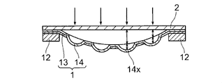
以上の例は、全体が一様な蒸着マスク1の例であったが、例えばスマートホンのような比較的小形のパネルを複数個纏めて蒸着する多面取りの蒸着マスクの場合もある。そのような蒸着マスク1は、その一例が図3Aに平面図で示されるように、金属膜13の開口内にアクティブ領域14が形成され、そのアクティブ領域14内に蒸着パターンに対応した精細な開口部が形成される。このアクティブ領域14は、全面が樹脂フィルムからなる場合もあるし、樹脂フィルムと金属支持層との複合マスクで形成される場合もある。いずれにしても、開口部が形成されることから、金属膜13の部分に比べて剛性が弱いため、金属膜13に対しても撓みやすい。その結果、図3Bに、撓みの中心部を通り、蒸着マスク1の一辺に沿って切断した断面が誇張して示されるように、本来の蒸着マスク1全体の撓み(周縁部を支点とする撓み)d0の他に、各アクティブ領域14の撓みh0(図3C参照)が存在することを本発明者らは見出した。そして、このアクティブ領域14での撓みh0による蒸着マスク1の長さの変化の部分も被蒸着基板2を伸ばさないと、被蒸着基板2と蒸着マスク1とを密着させられないことを本発明者らは見出した。
次に、このアクティブ領域14の撓みの影響の除去について説明がされる。図3Cに、1個のアクティブ領域14の撓みの状態が前述の蒸着マスク1の一辺に沿った撓みの中心部を通る断面図で簡略的に示されている。この例においても、前述の場合と同様に、撓みによりアクティブ領域14が撓んだ状態のアクティブ領域14の長さの半分の長さs1が直角三角形PQRの斜辺の長さで近似される。各アクティブ領域14の撓みh0も、実測により知り得る。アクティブ領域14の前述の断面での長さをs0とすると、撓んだ状態のアクティブ領域14の長さの半分s1は、
s1={h0 2+(s0/2)2}1/2
となる。従って、アクティブ領域14の長さの変化量Δsは、
Δs=2(s1-s0/2)=2{h0 2+(s0/2)2}1/2-s0・・・(4)
となる。このアクティブ領域14の長さの変化を相殺するために被蒸着基板をどのように押すかについては、2通りの方法が考えられる。
s1={h0 2+(s0/2)2}1/2
となる。従って、アクティブ領域14の長さの変化量Δsは、
Δs=2(s1-s0/2)=2{h0 2+(s0/2)2}1/2-s0・・・(4)
となる。このアクティブ領域14の長さの変化を相殺するために被蒸着基板をどのように押すかについては、2通りの方法が考えられる。
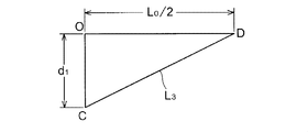
第1の方法は、図3Dに示されるように、蒸着マスク1を伸ばして、きれいな凹面とした状態にし、被蒸着基板2もその中心部を押して同じ凹面にすることにより、全面に亘って被蒸着基板2と蒸着マスク1とを密着させるという考え方である。この方法によれば、図3Eに近似の直角三角形OCDで示されるように、直角三角形OCDの斜辺の長さL3、すなわち蒸着マスク1のアクティブ領域14の長さの変化量Δsを考慮した蒸着マスク1の長さを求めれば、被蒸着基板2の押し込み量d1を得ることができる。なお、図3D~3Eでは、蒸着マスク1の撓みを考慮した弧の長さL3を三角形OCDの斜辺の長さで近似しているが、被蒸着基板2の押し込み後の形状も蒸着マスク1の形状とほぼ一致するため、三角形O’C’D’に近似できる。そのため、被蒸着基板2の押し込み量d1は、蒸着マスク1の周縁部を支点とする撓みによる蒸着マスク1の長さにアクティブ領域14の撓みを加味した後の撓みの深さ(OCの長さ)d1と一致する。
この蒸着マスク1の長さL3は、各アクティブ領域14の撓みによる長さの変化量Δsを加えた長さに等しいので、各アクティブ領域の長さの変化量Δsを前述の断面に沿ったアクティブ領域14の数だけ足すことにより得られる。今、断面にn個のアクティブ領域14があると、図3Eのように、蒸着マスク1の半分で考えると、アクティブ領域14の数はn/2個になる。アクティブ領域14の1個当たりの蒸着マスク1の長さの変化量は、前述のΔsであるため、図3Eの斜辺の長さL3は、
L3=L1+(n/2)Δs・・・・・・(5)
となる。なお、L1は式(1)により求まる。従って、図3Eより被蒸着基板2の押し込み量d1は、
d1={L3 2-(L0/2)2}1/2
となる。逆に言えば、蒸着マスク1の周縁部を支点とする撓みの中心部の鉛直線上の被蒸着基板2の上面で、d1の寸法だけ被蒸着基板2を押し込むことにより、被蒸着基板2と蒸着マスク1とが密着する。以上の説明では、熱膨張の影響を考慮していないが、熱膨張を考慮する場合は、前述の式(5)でL1に代えて式(3)のL2を用いればよい。
L3=L1+(n/2)Δs・・・・・・(5)
となる。なお、L1は式(1)により求まる。従って、図3Eより被蒸着基板2の押し込み量d1は、
d1={L3 2-(L0/2)2}1/2
となる。逆に言えば、蒸着マスク1の周縁部を支点とする撓みの中心部の鉛直線上の被蒸着基板2の上面で、d1の寸法だけ被蒸着基板2を押し込むことにより、被蒸着基板2と蒸着マスク1とが密着する。以上の説明では、熱膨張の影響を考慮していないが、熱膨張を考慮する場合は、前述の式(5)でL1に代えて式(3)のL2を用いればよい。
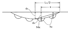
第2の方法は、図4Aに概略図が示されるように、各アクティブ領域14の撓みの中心部の鉛直線上で被蒸着基板2の上面を押すことにより、各アクティブ領域14において被蒸着基板2と蒸着マスク1とを密着させる方法である。この場合は、蒸着マスク1のアクティブ領域14の撓みに合せて被蒸着基板2も撓ませるというイメージである。この場合の各アクティブ領域14の押し込み量d3は、例えば図4Bに前述と同様の直角三角形に近似した図が示されているように、蒸着マスク1の周縁部を支点とする撓みの中心部でd0の押し込みが必要になるので、周縁部(フレーム12に固定された端縁)から距離xのところにあるアクティブ領域14xでは、図4Bに示されるように、蒸着マスク1の全体の撓み分d0のx/(L0/2)倍、すなわち2d0x/L0と、1個のアクティブ領域14の撓み量h0とを加えた量、すなわち
d3(x)=2d0x/L0+h0
で押し込むことによっても、被蒸着基板2と蒸着マスク1とを密着させることができる。
d3(x)=2d0x/L0+h0
で押し込むことによっても、被蒸着基板2と蒸着マスク1とを密着させることができる。
すなわち、この場合は、蒸着マスク1の周縁部を支点とする全体の撓みによる深さd0を、各アクティブ領域14xの位置に応じて按分してdxが求められ、アクティブ領域14自体の撓みは、各アクティブ領域で等しいとしてh0としている。この場合、被蒸着基板2がガラスのように剛性がある場合には、隣のアクティブ領域の押圧の影響があるため、実際の押し込み量を測定しながらその押し込み量になるように各アクティブ領域14で押圧される。しかし、被蒸着基板2が薄いガラス板やフレキシブル基板のように、余り剛性が無い場合、又はアクティブ領域14のピッチが大きい場合には、隣のアクティブ領域14の押圧による影響も少なく当初から設定した押し込み量で押し込むことができる。なお、図4Aで被蒸着基板2の上側の矢印線は、被蒸着基板2を押し込むための荷重をかける位置を示している。
この場合は、各アクティブ領域を別々の力で押す必要があるので、それぞれをプランジャーとアクチュエータなどの押圧手段などにより、別々に押し込むことが好ましい。各プランジャーの先端部は、前述のように、丸みを帯びた曲面であることが好ましい。特に、被蒸着基板がフレキシブル基板である場合には、プランジャーの先端が尖っていると、被蒸着基板2を破りやすくなるし、被蒸着基板2がガラスの場合でも、プランジャーの先端が尖っていると、破損しやすいからである。この場合も、前述の例と同様に、プランジャーの先端部はアクティブ領域14の撓みの曲率半径に応じた球面とされることが好ましく、さらにほぼ全面に亘ってそのような球面とされる押圧具30(図4C参照)が用いられることが好ましい。
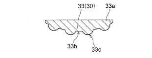
すなわち、前述の押圧具30を被蒸着基板2の広い範囲で当接させる場合には、図4Cに押圧具30の一例が凸部付き球欠体33で示されるように、蒸着マスク1の周縁部を支点とする撓みによる中央部で深く、周縁部で浅い形状の球欠部33bに、さらに各アクティブ領域14の位置でアクティブ領域14の撓みの凸部33cが形成された凸部付き球欠体33が用いられ得る。このような凸部付き球欠体33が用いられることにより、とくに被蒸着基板2がフレキシブル基板であれば、蒸着マスク1と被蒸着基板2とが完全に密着され得る。この場合の球欠部33bの曲率半径は、前述の式(2)による半径r、又はさらに熱膨張を加味したときのL2を用いたときの曲率半径で形成され、凸部33cの曲率半径は、図3Cから前述の図2Cと同様にして計算される曲率半径により形成される。なお、この場合も脚部33aが示されているが、この脚部33aのない球欠部33bが、タッチプレート41(図1B参照)と一体に形成されても、又は、接着もしくは重ねられてもよい。
本発明の蒸着装置は、例えば図1Aに示されるように、蒸着マスク1を載置するマスクホルダー15と、被蒸着基板2を保持できるように設けられる基板ホルダー29と、基板ホルダー29により保持される被蒸着基板2上に被蒸着基板2の周囲と接して設けられるタッチプレート41と、マスクホルダー15に載置される蒸着マスク1の基板ホルダー29と反対側に設けられ、蒸着材料を気化させる蒸着源5と、被蒸着基板2の上面を押圧する押圧装置3とを有している。その押圧装置3は、蒸着マスク1の撓み(蒸着マスク1の全体の撓み、又はアクティブ領域14などの個々の撓み)の中心部の鉛直線上で基板ホルダー29により保持される被蒸着基板2の上面の位置で押圧し得るように設けられている。図1Aに示される例では、押圧装置3が、タッチプレート41を利用した押圧具30により押し込む例で示されているが、これには限定されない。他の例が後述される。
この押圧装置3は、前述のように、場合によって、d0以上であってd2以下の量、又はd3(x)の量だけ被蒸着基板2を押し込めるように形成されている。この押圧装置3は、前述の図1A~1Bに示されるように、金属や剛性のあるプラスチックなどの種々の剛性体からなる押圧具30とタッチプレート41及びアクチュエータなどの押圧手段とで構成され得る。しかし、図示されていないが、プランジャーとアクチュエータなど、種々の押し込み装置を用いることができる。要は、いずれかの撓みの中心部で所定量の押し込みが行われるように形成されていることに特徴がある。なお、撓みの中心部だけでなく、その周囲から周縁部にかけて被蒸着基板2と当接する構成であれば、なお好ましい。
この例が、図1B及び図4Cに示されている。すなわち、図1Bに示される例が、図1Aと同様の蒸着マスク1の周縁部を支点とする撓みに倣った形状の球欠体32がタッチプレート41と被蒸着基板2との間に挿入されている。押圧具30の形状以外は図1Aに示される構造と同じで、同じ部分には同じ符号を付してその説明は省略される。この例も、球欠体32の一部(脚部32a)がタッチプレート41内に嵌め込まれるように形成されているが、嵌め込まれなくてもタッチプレート41に接着されてもよいし、タッチプレート41と一体で形成されてもよい。タッチプレート41から出っ張った部分の高さが所定量のdであればよい。この例でも、撓みの中心部での押し込み量は所定の寸法dになる。
また、前述の図4Aに相当する考え方で、このような面で接触させるには、図4Cに示されるように、蒸着マスク1の周縁部を支点とする撓みd0の場合の曲率半径r(式(2)によるr又はさらに熱膨張を加味した曲率半径)による球欠部33bの外周上に、アクティブ領域14の撓みに応じた曲率半径を有する断面円弧状の凸部33cが形成された形状の凸部付き球欠体33にした押圧具30が用いられることにより、被蒸着基板2と蒸着マスク1とが密着され得る。この場合のアクティブ領域14の凸部33cの球面の曲率半径も前述のように図3Cから求められる。
基板ホルダー29は、複数のフック状のアームで被蒸着基板2の周縁部を保持し、上下に昇降できるように図示しない駆動装置に接続されている。ロボットアームにより蒸着装置内に搬入された被蒸着基板2をフック状のアームで受け取り、被蒸着基板2が蒸着マスク1に近接するまで基板ホルダー29が下降する。そして位置合せを行えるように図示しない撮像装置も設けられている。タッチプレート41は支持フレーム42により支持され、図1Aに示される例では、球体(押圧具)31を挟んでタッチプレート41を被蒸着基板2の周縁部に接するまで押し下げることにより、被蒸着基板2を蒸着マスク1と密着させることができる。そのアクチュエータなどからなる押圧手段も図示されていないが備えている。タッチプレート41は、元々被蒸着基板2を平坦にするために設けられており、剛性を有する板材で形成されている。そのため、図1Aに示されるような鋼球からなる球体31のような押圧具30を押してもタッチプレート41は変形することなく、平行に押し下げて被蒸着基板2の周縁部と密着させることにより、被蒸着基板2が変形する。
この球体31は、タッチプレート41と被蒸着基板2との間の距離が所定の押し込み量dになる高さを有している。すなわち、図1Aに示される例では、球体31の一部がタッチプレート41に入り込む構造になっていることにより、球体31の直径は、所定寸法のdよりも大きく形成され、タッチプレート41から露出する部分の長さが所定寸法dになるように形成されている。このような構造にされることにより、球体31が横方向には移動することなく、タッチプレート41の上下移動に伴って上下のみに移動する。その結果、被蒸着基板2の撓みが蒸着マスク1の撓みと一致し、相互に密着する。しかし、押圧装置3は、このような構成ではなく、プランジャーとアクチュエータとで押し下げる構成でもよい。この場合、タッチプレート41に貫通孔を設けて、その貫通孔を介して被蒸着基板2を押圧できるようにすることが好ましい。タッチプレート41は前述のように剛性があり、タッチプレート41を押圧しても平坦面で押圧することになり、圧力が分散して、撓みの中心部で被蒸着基板2を押すことができないからである。要は、撓みの中心部で被蒸着基板2が押されることが必要である。
なお、タッチプレート41は、図示されていないが内部に冷却水を循環させることにより、被蒸着基板2及び蒸着マスク1を冷却する機能も有し得る。押圧装置3は、この例のように、押圧具30を有しなくても、タッチプレート41の被蒸着基板2と当接する部分が、前述の押圧具30の被蒸着基板2と当接する部分の形状で、かつ、所定の寸法dの高さになる曲面であればよい。
なお、この被蒸着基板2が押し下げられる前に被蒸着基板2と蒸着マスク1とが位置合せされる。その位置合せの際には、蒸着マスク1と被蒸着基板2のそれぞれに形成されたアライメントマークを撮像しながら、被蒸着基板2を蒸着マスク1に対して相対的に移動させる。そのため、図示されていないが、アライメントマークを撮像する撮像装置や被蒸着基板2を微動する微動装置も備えている。さらに、図1Aには図示されていないが、この全体は、チャンバ内に入れられ、チャンバ内を真空にする真空装置も備えられている。
蒸着マスク1としては、例えば樹脂フィルムのみで形成されるものや、樹脂フィルムと金属支持層とが積層されたハイブリッド型のもの、また、複数のパネル分を纏めて形成された多面取りのマスク、メタルマスクなど種々の蒸着マスクに適用することができる。
この蒸着マスク1に樹脂フィルムが用いられる場合、樹脂フィルムとしては、被蒸着基板2との線膨張係数の差が小さいことが好ましいが、特に限定されない。例えばポリイミド(PI)樹脂、ポリエチレンナフタレート(PEN)樹脂、ポリエチレンテレフタレート(PET)樹脂、シクロオレフィンポリマー(COP)樹脂、環状オレフィンコポリマー(COC)樹脂、ポリカーボネート(PC)樹脂、ポリアミド樹脂、ポリアミドイミド樹脂、ポリエステル樹脂、ポリエチレン樹脂、ポリビニルアルコール樹脂、ポリプロピレン樹脂、ポリスチレン樹脂、ポリアクリロニトリル樹脂、エチレン酢酸ビニルコポリマー樹脂、エチレン-ビニルアルコールコポリマー樹脂、エチレン-メタクリル酸コポリマー樹脂、ポリ塩化ビニル樹脂、ポリ塩化ビニリデン樹脂、セロファン、アイオノマー樹脂などを使用することができる。ポリイミド樹脂は、前駆体溶液を塗布し、加熱処理を行って樹脂フィルムを形成させる場合、その加熱処理の際の昇温のプロファイルなどの条件により、線膨張係数を調整することができるので好ましいが、これに限定されるものではない。樹脂フィルムの厚さは数μm~数十μm程度、例えば5μm以上であって10μm以下程度である。
金属支持層が形成される場合、磁性体が用いられることにより、図示しない被蒸着基板2の蒸着マスク1と反対側に設けられるマグネットにより磁気吸着をさせることができるが、これに限定されない。この金属支持層が設けられる場合には、樹脂フィルムに形成される開口部よりもひと回り大きい開口が金属支持層に形成される。この金属支持層の厚さは、5μm以上であって30μm以下程度に形成される。また、多面取りの場合は、例えば図3Aに示されるように、金属層13内に各パネルに対応する部分であるアクティブ領域14が形成される。アクティブ領域14は、樹脂フィルムのみからなり、開口部が形成されてもよいし、このアクティブ領域14内でも、開口部の周囲に金属支持層が形成されてもよい。金属支持層と金属層とは同じものでもよいし、別途形成されたアクティブ領域14が金属層13の開口部に貼り付けられてもよい。この金属層13は被蒸着基板2との線膨張率の差が小さいことが好ましく、熱による膨張が殆どないことから、インバー(FeとNiの合金)が特に好ましい。
この蒸着マスク1は、近年大形化しており、一辺が1mを超す大きなものになっている。しかも樹脂フィルムにしろ、金属支持層や金属層13にしろ、非常に薄い膜であるため、蒸着マスク1の周囲がフレーム12により固定されていても、図1Aに示されるように、フレーム12の部分で水平に保持されると、撓みが生じてくる。このような撓みが生じないように、樹脂フィルムなどのマスク材料がフレームに貼り付けられる前に、マスク材料の四方から張力をかけて(架張して)フレーム12に貼り付けられる。しかし、それでも非常に薄い膜で1m以上の大きい枠体(フレーム12)に貼り付けられて水平に保持されると、撓みが生じ、この撓みを防止することは不可能に近い。そのため、前述のように、本発明では、この蒸着マスク1の撓みに被蒸着基板2を追随させている。しかし、蒸着マスク1の撓みは、自重による撓みだけではなく、熱膨張による撓みも加わり得る。さらに、前述の多面取りの蒸着マスクのように、金属層13とアクティブ領域14とが混在する場合には、材料の剛性の差に基づき、アクティブ領域14で特に撓みが生じやすい、などの種々の問題もある。すなわち、一概に蒸着マスク1の撓み分だけ被蒸着基板2を押し込めばよいというものではないことを本発明者らは見出した。そして、前述のように、蒸着マスク1の種々の撓みを考慮して、蒸着マスク1の撓みの中心軸上で、被蒸着基板2を押し込むことで、被蒸着基板2と蒸着マスク1とを密着させ得ることを本発明者らが見出した。
フレーム12は、特に熱膨張の小さいインバーなどが用いられる。また、樹脂フィルムや金属支持層のように薄い膜ではなく、25mm以上であって50mm以下程度と厚いため、撓みや熱に対しても強固である。そのため、撓みは、専ら樹脂フィルムや金属支持層(金属層13)の部分に生じる。この撓みは、湾曲状になるため、ほぼ円弧に近い。一方、被蒸着基板2は、有機EL表示装置の場合は、ガラス基板又は樹脂フィルムなどからなるフレキシブル基板が用いられる。ガラスの場合は、小刻みな変形はし難いため、一点で押しても湾曲状になりやすい。すなわち、蒸着マスク1の撓みの中心部上で被蒸着基板2の上面を押すことにより、蒸着マスク1の湾曲と重なりやすい。従って、前述の撓みの深さを求めるのに、実際の(曲面の)蒸着マスク1の長さを直角三角形の斜辺の長さで近似したが、被蒸着基板2の形状も同様であるため、その誤差は非常に小さい。被蒸着基板2がフレキシブル基板であっても、押される部分が蒸着マスク1の弧形と相応する弧形になっていれば、同様の湾曲状になりやすい。そこで、蒸着マスク1が周縁部を支点とする、自重による撓みだけであれば、図1Aに示されるように、蒸着マスク1の撓みの中心部と鉛直方向で、被蒸着基板2の上面から図2Aに示される蒸着マスク1の撓み量d0だけ押し込まれることにより、蒸着マスク1と被蒸着基板2とが同じ曲線(曲面)で密着しやすい。
蒸着源5は、点状、線状、面状など、種々の蒸着源が用いられ得るが、例えばるつぼが線状に並べて形成されたリニア型の蒸着源5(図1Aの紙面と垂直方向に伸びている)、いわゆるリニアソースが、例えば紙面の左端から右端まで操作されることにより、全面に蒸着が行われる。この蒸着源5は、前述のように、るつぼの形状により定まる蒸着材料の放射ビームの断面形状の側縁が、一定角度を有する断面扇形の形状で、蒸着材料を放射する。この扇形の断面形状の一番側壁側の蒸着粒子でも、蒸着マスク1に遮られることなく、被蒸着基板2の所定の場所に届くように、蒸着マスク1の開口部の近傍はテーパ状などに形成されている。
次に、本発明の蒸着方法を用いて有機EL表示装置を製造する方法が説明される。蒸着方法以外の製造方法は、周知の方法で行えるため、本発明の蒸着方法により有機層を積層する方法を主として、図5A~5Bを参照しながら説明する。
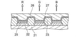
本発明の有機EL表示装置の製造方法は、図示しない支持基板上に図示しないTFT、平坦化膜及び第1電極(例えば陽極)22が形成された装置基板21上に前述の方法により製造された蒸着マスク1を位置合せして重ね合せ、有機材料51が蒸着されることにより有機層の積層膜25が形成される。そして、積層膜25上に第2電極26(陰極)が形成される。
装置基板21は、図示されていないが、例えばガラス板などの支持基板に、各画素のRGBサブ画素ごとにTFTなどのスイッチ素子が形成され、そのスイッチ素子に接続された第1電極22が、平坦化膜上に、AgあるいはAPCなどの金属膜と、ITO膜との組み合せにより形成されている。サブ画素間には、図5A~5Bに示されるように、サブ画素間を区分するSiO2又はアクリル樹脂、ポリイミド樹脂などからなる絶縁バンク23が形成されている。このような装置基板21の絶縁バンク23上に、前述の蒸着マスク1が位置合せして固定される。この固定は、一般的には、前述のように、例えば装置基板21の蒸着面と反対側に設けられる磁石などにより、吸着することにより行われる。しかし、本発明では、蒸着マスク1を吸着させる必要は少ないので、いわゆる磁気チャックを使用する必要はない。タッチプレー41で装置基板21が押し付けられることにより蒸着マスク1と装置基板21の絶縁バンク23とが密着して固定される。
この状態で、図5Aに示されるように、蒸着装置内で蒸着源(るつぼ)5から有機材料51が放射され、蒸着マスク1の開口部11a上の部分のみの装置基板21上に有機材料51が蒸着され、所望のサブ画素の第1電極22上に有機層の積層膜25が形成される。蒸着マスク1の開口部11aは、絶縁バンク23の表面の間隔より小さく形成されているので、絶縁バンク23の側壁には有機材料51は堆積され難くなっている。その結果、図5A~5Bに示されるように、ほぼ、第1電極22上のみに有機層の積層膜25が堆積される。この蒸着工程が、順次蒸着マスク1が変えられ、各サブ画素に行われる。複数のサブ画素に同時に同じ材料が蒸着される蒸着マスクが用いられる場合もある。本発明によれば、蒸着マスク1が装置基板21の絶縁バンク23上に密着しているため、非常に正確な有機層の積層膜25が得られる。
図5A~5Bでは、有機層の積層膜25が簡単に1層で示されているが、実際には、有機層の積層膜25は、異なる材料からなる複数層の積層膜で形成される。例えば陽極22に接する層として、正孔の注入性を向上させるイオン化エネルギーの整合性の良い材料からなる正孔注入層が設けられる場合がある。この正孔注入層上に、正孔の安定な輸送を向上させると共に、発光層への電子の閉じ込め(エネルギー障壁)が可能な正孔輸送層が、例えばアミン系材料により形成される。さらに、その上に発光波長に応じて選択される発光層が、例えば赤色、緑色に対してはAlq3に赤色又は緑色の有機物蛍光材料がドーピングされて形成される。また、青色系の材料としては、DSA系の有機材料が用いられる。発光層の上には、さらに電子の注入性を向上させると共に、電子を安定に輸送する電子輸送層が、Alq3などにより形成される。これらの各層がそれぞれ数十nm程度ずつ積層されることにより有機層の積層膜25が形成されている。なお、この有機層と金属電極との間にLiFやLiqなどの電子の注入性を向上させる電子注入層が設けられることもある。
有機層の積層膜25のうち、発光層は、RGBの各色に応じた材料の有機層が堆積される。また、正孔輸送層、電子輸送層などは、発光性能を重視すれば、発光層に適した材料で別々に堆積されることが好ましい。しかし、材料コストの面を勘案して、RGBの2色又は3色に共通して同じ材料で積層される場合もある。2色以上のサブ画素で共通する材料が積層される場合には、共通するサブ画素に開口が形成された蒸着マスクが形成される。個々のサブ画素で蒸着層が異なる場合には、例えばRのサブ画素で1つの蒸着マスク1を用いて、各有機層を連続して蒸着することができるし、RGBで共通の有機層が堆積される場合には、その共通層の下側まで、各サブ画素の有機層の蒸着がなされ、共通の有機層のところで、RGBに開口が形成された蒸着マスク1を用いて一度に全画素の有機層の蒸着がなされる。
そして、全ての有機層の積層膜25及びLiF層などの電子注入層の形成が終了したら、蒸着マスク1が分離され、第2電極(例えば陰極)26が全面に形成される。図5Bに示される例は、トップエミッション型で、上側から光を出す方式になっているので、第2電極26は透光性の材料、例えば、薄膜のMg-Ag共晶膜により形成される。その他にAlなどが用いられ得る。なお、装置基板21側から光が放射されるボトムエミッション型の場合には、第1電極22にITO、In3O4などが用いられ、第2電極26としては、仕事関数の小さい金属、例えばMg、K、Li、Alなどが用いられ得る。この第2電極26の表面には、例えばSi3N4などからなる保護膜27が形成される。なお、この全体は、図示しないガラス、樹脂フィルムなどからなるシール層により封止され、有機層の積層膜25が水分を吸収しないように構成される。また、有機層はできるだけ共通化し、その表面側にカラーフィルタを設ける構造にすることもできる。この蒸着マスク1は繰り返し使用することができる。
1 蒸着マスク
2 被蒸着基板
3 押圧装置
5 蒸着源
12 フレーム
13 金属層
14 アクティブ領域
15 マスクホルダー
21 装置基板
22 第1電極
23 絶縁バンク
25 積層膜
26 第2電極
27 保護膜
29 基板ホルダー
30 押圧具
31 球体
32 球欠体
32a 脚部
33 凸部付き球欠体
33a 脚部
33b 球欠部
33c 凸部
41 タッチプレート
42 支持フレーム
2 被蒸着基板
3 押圧装置
5 蒸着源
12 フレーム
13 金属層
14 アクティブ領域
15 マスクホルダー
21 装置基板
22 第1電極
23 絶縁バンク
25 積層膜
26 第2電極
27 保護膜
29 基板ホルダー
30 押圧具
31 球体
32 球欠体
32a 脚部
33 凸部付き球欠体
33a 脚部
33b 球欠部
33c 凸部
41 タッチプレート
42 支持フレーム
Claims (20)
- 蒸着マスクを周縁部で保持して水平方向に配置し、前記蒸着マスクの上面側に蒸着膜を形成する被蒸着基板を重ねて配置し、前記蒸着マスクの下方に蒸着源を配置し、前記蒸着源から蒸着材料を気化させて前記被蒸着基板に蒸着膜を形成する蒸着方法であって、
前記蒸着マスクの撓みの中心部の鉛直方向で、前記被蒸着基板の上面の位置から、前記蒸着マスクの周縁部を支点とする撓みの深さ、又はそれを超える量の前記被蒸着基板の押し込みを行い、前記被蒸着基板と前記蒸着マスクとを密着させながら蒸着することを特徴とする蒸着方法。 - 前記蒸着マスクの撓みの深さ、又はそれを超える量を押し込むことは、前記蒸着マスクの周縁部である支点及び前記蒸着マスクの撓みの中心部を結ぶ弧の長さと、前記支点の位置に接する前記被蒸着基板の前記蒸着マスク側の位置、及び前記撓みの中心部の鉛直線と交わる前記被蒸着基板の前記蒸着マスク側の面の位置を結ぶ前記被蒸着基板の弧の長さとがほぼ等しくなるように押し込むことである請求項1記載の蒸着方法。
- 前記蒸着マスクの弧の長さに、蒸着時の温度上昇による熱膨張による伸びを加える請求項2記載の蒸着方法。
- 前記蒸着マスクが、開口部パターンが形成されるアクティブ領域を複数個有し、前記アクティブ領域の各々の撓みによる前記アクティブ領域の弧の長さの変化量を、前記周縁部を支点とする撓みのときの前記蒸着マスクの弧の長さに加える請求項2又は3記載の蒸着方法。
- 前記蒸着マスクの前記周縁部を支点とする撓み時の弧の長さを、前記蒸着マスクの撓みの中心部を通る、蒸着マスクの一辺に沿った方向に切断した断面での長さとし、前記弧の長さを前記周縁部の支点と前記撓みの中心部とを結ぶ線分の長さで近似する請求項2~4のいずれか1項に記載の蒸着方法。
- 前記アクティブ領域の撓み時の前記アクティブ領域の弧の長さを、前記アクティブ領域の撓みの中心部を通る、前記蒸着マスクの一辺に沿った方向に切断した断面での長さとし、前記撓みの中心部と前記アクティブ領域の端部を結ぶ線分の長さで近似する請求項4記載の蒸着方法。
- 前記蒸着マスクが、開口部パターンが形成されるアクティブ領域を複数個有し、前記アクティブ領域の各々の撓みh0と、前記アクティブ領域の各々の位置における前記蒸着マスクの周縁部からの距離xに応じて計算される、前記蒸着マスクの周縁部を支点とする撓みdxとの和に相当する量d3(x)(=h0+dx)の押し込み量で、前記アクティブ領域の各々の中心部の鉛直方向で、前記被蒸着基板の上面の位置から前記被蒸着基板を押し込む請求項1~3のいずれか1項に記載の蒸着方法。
- 前記被蒸着基板の押し込みを、先端部が前記蒸着マスクの撓みの曲率半径を半径とする球面に形成された押圧具により行う請求項1~7のいずれか1項に記載の蒸着方法。
- 蒸着マスクを載置するマスクホルダーと、被蒸着基板を保持できるように設けられる基板ホルダーと、前記基板ホルダーにより保持される被蒸着基板上に接して設けられるタッチプレートと、前記マスクホルダーに載置される蒸着マスクの前記基板ホルダーと反対側に設けられ、蒸着材料を気化させる蒸着源と、前記被蒸着基板の上面を押圧する押圧装置とを有し、前記押圧装置が、前記蒸着マスクの撓みの中心部の鉛直線上で前記基板ホルダーにより保持される被蒸着基板の上面の位置で押圧し得るように設けられてなる蒸着装置。
- 前記押圧装置が、前記蒸着マスクの周縁部を支点とする撓みの中心部の鉛直線上で前記被蒸着基板の上面を押圧するように形成され、かつ、前記蒸着マスクの周縁部を支点とする撓みの深さ、又はそれを超える量の押し込み量になるように形成されている請求項9記載の蒸着装置。
- 前記蒸着マスクの撓みの深さ、又はそれを超える押し込み量は、前記蒸着マスクの周縁部である支点及び前記蒸着マスクの撓みの中心部を結ぶ弧の長さと、前記支点の位置に接する前記被蒸着基板の前記蒸着マスク側の位置、及び前記撓みの中心部の鉛直線と交わる前記被蒸着基板の前記蒸着マスク側の面の位置を結ぶ前記被蒸着基板の弧の長さとをほぼ等しくなるようにする押し込み量である請求項10記載の蒸着装置。
- 前記蒸着マスクの弧の長さに、蒸着時の温度上昇による熱膨張による伸びを加える請求項11記載の蒸着方法。
- 前記蒸着マスクが、開口部パターンが形成されるアクティブ領域を複数個有し、前記アクティブ領域の各々の撓みによる前記アクティブ領域の弧の長さの変化量を、前記周縁部を支点とする撓みのときの前記蒸着マスクの弧の長さに加えた値を前記蒸着マスクの弧の長さとする請求項11又は12記載の蒸着装置。
- 前記蒸着マスクが、開口部パターンが形成されるアクティブ領域を複数個有し、前記押圧装置が、前記アクティブ領域のそれぞれの撓みの中心部の鉛直線上で所定の量だけ押し下げるように形成されてなる請求項8または9記載の蒸着装置。
- 前記所定の量が、前記アクティブ領域の各々の撓みh0と、前記アクティブ領域の各々の位置における前記蒸着マスクの周縁部からの距離xに応じて計算される、前記蒸着マスクの周縁部を支点とする撓みdxとの和に相当する量d3(x)(=h0+dx)である請求項14記載の蒸着装置。
- 前記押圧装置が、前記タッチプレートと前記被蒸着基板との間が所定の寸法となる押圧具と、前記タッチプレートを押圧する手段とからなる請求項10~13のいずれか1項に記載の蒸着装置。
- 前記押圧具は、少なくとも前記被蒸着基板側が曲面であり、前記タッチプレート側が前記タッチプレート内に一部嵌め込まれる構造である請求項16記載の蒸着装置。
- 前記押圧具の前記被蒸着基板と当接する面が、前記蒸着マスクの撓みの曲率半径を半径とする球面に形成されてなる請求項16または17記載の蒸着装置。
- 前記押圧装置が、前記タッチプレートに形成される貫通孔を通して前記被蒸着基板を直接押し付けるプランジャーと該プランジャーを押し込む押圧手段とからなる請求項9~15のいずれか1項に記載の蒸着装置。
- 装置基板上に有機層を積層して有機EL表示装置を製造する方法であって、
支持基板上にTFTおよび第1電極を少なくとも形成した前記装置基板上に請求項1~7のいずれか1項に記載の蒸着方法を用いて前記第1電極上に有機材料を蒸着することで有機層の積層膜を形成し、前記積層膜上に第2電極を形成することを含む有機EL表示装置の製造方法。
Priority Applications (4)
| Application Number | Priority Date | Filing Date | Title |
|---|---|---|---|
| US16/087,094 US11319624B2 (en) | 2016-03-23 | 2016-07-22 | Vapor deposition apparatus, vapor deposition method, and method for manufacturing organic EL display apparatus |
| CN201680083566.2A CN109072402B (zh) | 2016-03-23 | 2016-07-22 | 蒸镀装置、蒸镀方法及有机el显示装置的制造方法 |
| JP2018506748A JP6407479B2 (ja) | 2016-03-23 | 2016-07-22 | 蒸着装置、蒸着方法及び有機el表示装置の製造方法 |
| US17/709,864 US12319995B2 (en) | 2016-03-23 | 2022-03-31 | Vapor deposition apparatus, vapor deposition method, and method for manufacturing organic EL display apparatus |
Applications Claiming Priority (2)
| Application Number | Priority Date | Filing Date | Title |
|---|---|---|---|
| JP2016058695 | 2016-03-23 | ||
| JP2016-058695 | 2016-03-23 |
Related Child Applications (2)
| Application Number | Title | Priority Date | Filing Date |
|---|---|---|---|
| US16/087,094 A-371-Of-International US11319624B2 (en) | 2016-03-23 | 2016-07-22 | Vapor deposition apparatus, vapor deposition method, and method for manufacturing organic EL display apparatus |
| US17/709,864 Division US12319995B2 (en) | 2016-03-23 | 2022-03-31 | Vapor deposition apparatus, vapor deposition method, and method for manufacturing organic EL display apparatus |
Publications (1)
| Publication Number | Publication Date |
|---|---|
| WO2017163440A1 true WO2017163440A1 (ja) | 2017-09-28 |
Family
ID=59901020
Family Applications (1)
| Application Number | Title | Priority Date | Filing Date |
|---|---|---|---|
| PCT/JP2016/071623 Ceased WO2017163440A1 (ja) | 2016-03-23 | 2016-07-22 | 蒸着装置、蒸着方法及び有機el表示装置の製造方法 |
Country Status (5)
| Country | Link |
|---|---|
| US (2) | US11319624B2 (ja) |
| JP (2) | JP6407479B2 (ja) |
| CN (1) | CN109072402B (ja) |
| TW (1) | TWI626777B (ja) |
| WO (1) | WO2017163440A1 (ja) |
Cited By (2)
| Publication number | Priority date | Publication date | Assignee | Title |
|---|---|---|---|---|
| JP2018199865A (ja) * | 2016-03-23 | 2018-12-20 | 鴻海精密工業股▲ふん▼有限公司 | 蒸着装置、蒸着方法及び有機el表示装置の製造方法 |
| US11326246B2 (en) | 2020-07-27 | 2022-05-10 | Rockwell Collins, Inc. | Controlled warping of shadow mask tooling for improved reliability and miniturization via thin film deposition |
Families Citing this family (4)
| Publication number | Priority date | Publication date | Assignee | Title |
|---|---|---|---|---|
| CN111575655A (zh) * | 2020-06-24 | 2020-08-25 | 合肥维信诺科技有限公司 | 冷却板和蒸镀装置 |
| KR20230020035A (ko) * | 2021-08-02 | 2023-02-10 | 삼성디스플레이 주식회사 | 증착용 마스크 |
| CN114351106A (zh) * | 2021-12-29 | 2022-04-15 | 武汉华星光电半导体显示技术有限公司 | 蒸镀装置、蒸镀装置中的基板弯曲调节方法 |
| CN116970930B (zh) * | 2023-08-09 | 2025-09-05 | 拓荆科技(上海)有限公司 | 加热盘、薄膜沉积设备及薄膜沉积方法 |
Citations (7)
| Publication number | Priority date | Publication date | Assignee | Title |
|---|---|---|---|---|
| JP2005206939A (ja) * | 2003-12-26 | 2005-08-04 | Seiko Epson Corp | 薄膜形成方法、薄膜形成装置、有機エレクトロルミネッセンス装置の製造方法、有機エレクトロルミネッセンス装置、及び電子機器 |
| JP2005281746A (ja) * | 2004-03-29 | 2005-10-13 | Seiko Epson Corp | 蒸着装置、蒸着方法、電気光学装置、および電子機器 |
| JP2007207632A (ja) * | 2006-02-03 | 2007-08-16 | Canon Inc | マスク成膜方法およびマスク成膜装置 |
| JP2008059757A (ja) * | 2006-08-29 | 2008-03-13 | Canon Inc | 有機発光表示装置の製造方法 |
| JP2008108596A (ja) * | 2006-10-26 | 2008-05-08 | Seiko Epson Corp | マスク蒸着法、およびマスク蒸着装置 |
| JP2010031345A (ja) * | 2008-07-31 | 2010-02-12 | Canon Inc | 成膜装置及びそれを用いた成膜方法 |
| JP2012052155A (ja) * | 2010-08-31 | 2012-03-15 | Canon Inc | 真空成膜用マスクユニット及びこれを備えた真空成膜装置 |
Family Cites Families (18)
| Publication number | Priority date | Publication date | Assignee | Title |
|---|---|---|---|---|
| CH654596A5 (de) * | 1983-09-05 | 1986-02-28 | Balzers Hochvakuum | Verdampferzelle. |
| JP3881569B2 (ja) * | 2002-03-13 | 2007-02-14 | 株式会社堀場エステック | 液体材料気化装置 |
| JP4363401B2 (ja) * | 2003-03-26 | 2009-11-11 | 信越半導体株式会社 | 熱処理用ウェーハ支持具及び熱処理装置 |
| TWI249821B (en) | 2003-12-26 | 2006-02-21 | Seiko Epson Corp | Thin film formation method, thin film formation equipment, method of manufacturing organic electroluminescence device, organic electroluminescence device, and electronic apparatus |
| US7019268B2 (en) * | 2004-02-23 | 2006-03-28 | Asml Netherlands B.V. | Wafer processing apparatus and method of use |
| JP4418262B2 (ja) * | 2004-03-12 | 2010-02-17 | 三井造船株式会社 | 基板・マスク固定装置 |
| EP1672715A1 (de) * | 2004-12-17 | 2006-06-21 | Applied Films GmbH & Co. KG | Vorrichtung für die Beschichtung eines Substrats |
| DE102005013875A1 (de) * | 2005-03-24 | 2006-11-02 | Creaphys Gmbh | Heizeinrichtung, Beschichtungsanlage und Verfahren zur Verdampfung oder Sublimation von Beschichtungsmaterialien |
| US8633052B2 (en) * | 2008-04-18 | 2014-01-21 | 1366 Technologies Inc. | Wedge imprint patterning of irregular surface |
| KR101517020B1 (ko) | 2008-05-15 | 2015-05-04 | 삼성디스플레이 주식회사 | 유기전계발광표시장치의 제조장치 및 제조방법 |
| WO2010019213A2 (en) * | 2008-08-11 | 2010-02-18 | Veeco Instruments Inc. | Vacuum deposition sources having heated effusion orifices |
| JP2010180438A (ja) | 2009-02-04 | 2010-08-19 | Mitsubishi Electric Corp | マスクユニットおよびマスクユニットを有する蒸着装置 |
| RU2011142784A (ru) * | 2009-03-23 | 2013-04-27 | Конинклейке Филипс Электроникс Н.В. | Манипуляция магнитными частицами в биологическом образце |
| GB2468870B (en) * | 2009-03-25 | 2016-08-03 | Peratech Holdco Ltd | Sensor |
| JP2011233510A (ja) * | 2010-04-05 | 2011-11-17 | Canon Inc | 蒸着装置 |
| JP2012092395A (ja) * | 2010-10-27 | 2012-05-17 | Canon Inc | 成膜方法及び成膜装置 |
| US9543186B2 (en) * | 2013-02-01 | 2017-01-10 | Applied Materials, Inc. | Substrate support with controlled sealing gap |
| JP6407479B2 (ja) * | 2016-03-23 | 2018-10-17 | 鴻海精密工業股▲ふん▼有限公司 | 蒸着装置、蒸着方法及び有機el表示装置の製造方法 |
-
2016
- 2016-07-22 JP JP2018506748A patent/JP6407479B2/ja active Active
- 2016-07-22 CN CN201680083566.2A patent/CN109072402B/zh active Active
- 2016-07-22 US US16/087,094 patent/US11319624B2/en active Active
- 2016-07-22 WO PCT/JP2016/071623 patent/WO2017163440A1/ja not_active Ceased
- 2016-07-29 TW TW105124042A patent/TWI626777B/zh active
-
2018
- 2018-07-31 JP JP2018144200A patent/JP6782743B2/ja active Active
-
2022
- 2022-03-31 US US17/709,864 patent/US12319995B2/en active Active
Patent Citations (7)
| Publication number | Priority date | Publication date | Assignee | Title |
|---|---|---|---|---|
| JP2005206939A (ja) * | 2003-12-26 | 2005-08-04 | Seiko Epson Corp | 薄膜形成方法、薄膜形成装置、有機エレクトロルミネッセンス装置の製造方法、有機エレクトロルミネッセンス装置、及び電子機器 |
| JP2005281746A (ja) * | 2004-03-29 | 2005-10-13 | Seiko Epson Corp | 蒸着装置、蒸着方法、電気光学装置、および電子機器 |
| JP2007207632A (ja) * | 2006-02-03 | 2007-08-16 | Canon Inc | マスク成膜方法およびマスク成膜装置 |
| JP2008059757A (ja) * | 2006-08-29 | 2008-03-13 | Canon Inc | 有機発光表示装置の製造方法 |
| JP2008108596A (ja) * | 2006-10-26 | 2008-05-08 | Seiko Epson Corp | マスク蒸着法、およびマスク蒸着装置 |
| JP2010031345A (ja) * | 2008-07-31 | 2010-02-12 | Canon Inc | 成膜装置及びそれを用いた成膜方法 |
| JP2012052155A (ja) * | 2010-08-31 | 2012-03-15 | Canon Inc | 真空成膜用マスクユニット及びこれを備えた真空成膜装置 |
Cited By (4)
| Publication number | Priority date | Publication date | Assignee | Title |
|---|---|---|---|---|
| JP2018199865A (ja) * | 2016-03-23 | 2018-12-20 | 鴻海精密工業股▲ふん▼有限公司 | 蒸着装置、蒸着方法及び有機el表示装置の製造方法 |
| US11319624B2 (en) | 2016-03-23 | 2022-05-03 | Hon Hai Precision Industry Co., Ltd. | Vapor deposition apparatus, vapor deposition method, and method for manufacturing organic EL display apparatus |
| US12319995B2 (en) | 2016-03-23 | 2025-06-03 | Hon Hai Precision Industry Co., Ltd. | Vapor deposition apparatus, vapor deposition method, and method for manufacturing organic EL display apparatus |
| US11326246B2 (en) | 2020-07-27 | 2022-05-10 | Rockwell Collins, Inc. | Controlled warping of shadow mask tooling for improved reliability and miniturization via thin film deposition |
Also Published As
| Publication number | Publication date |
|---|---|
| JP6407479B2 (ja) | 2018-10-17 |
| CN109072402A (zh) | 2018-12-21 |
| US11319624B2 (en) | 2022-05-03 |
| TW201803182A (zh) | 2018-01-16 |
| CN109072402B (zh) | 2021-02-09 |
| US12319995B2 (en) | 2025-06-03 |
| TWI626777B (zh) | 2018-06-11 |
| JPWO2017163440A1 (ja) | 2018-07-05 |
| JP2018199865A (ja) | 2018-12-20 |
| US20210189543A1 (en) | 2021-06-24 |
| JP6782743B2 (ja) | 2020-11-11 |
| US20220220600A1 (en) | 2022-07-14 |
Similar Documents
| Publication | Publication Date | Title |
|---|---|---|
| JP6407479B2 (ja) | 蒸着装置、蒸着方法及び有機el表示装置の製造方法 | |
| KR102420460B1 (ko) | 마스크 프레임 조립체, 표시 장치의 제조 장치 및 표시 장치의 제조 방법 | |
| KR101730498B1 (ko) | 유기층 증착 장치 및 이를 이용한 유기 발광 디스플레이 장치의 제조 방법 | |
| US10224350B2 (en) | Mask for deposition, apparatus for manufacturing display apparatus having the same, and method of manufacturing display apparatus with manufacturing display apparatus having mask for deposition | |
| KR100696550B1 (ko) | 증착 장치 | |
| US8701592B2 (en) | Mask frame assembly, method of manufacturing the same, and method of manufacturing organic light-emitting display device using the mask frame assembly | |
| JP6345901B2 (ja) | 蒸着マスク、蒸着マスクの製造方法、蒸着方法および有機el表示装置の製造方法 | |
| KR102432350B1 (ko) | 마스크 프레임 조립체, 이를 포함하는 증착 장치 및 표시 장치의 제조 방법 | |
| JP2004349101A (ja) | 膜形成方法、膜形成装置、有機エレクトロルミネッセンス装置の製造方法、有機エレクトロルミネッセンス装置 | |
| KR102424976B1 (ko) | 마스크 조립체, 이를 이용한 표시 장치의 제조장치 및 표시 장치의 제조방법 | |
| WO2017145402A1 (ja) | 蒸着マスク、蒸着マスクの製造方法および有機el表示装置の製造方法 | |
| US10790447B2 (en) | Mask for thin film deposition, method of manufacturing the same, and method of manufacturing a display apparatus using the same | |
| JP2008156686A (ja) | マスクおよびマスク蒸着装置 | |
| JP2020056096A (ja) | マスク組立体及びそれを利用した表示装置の製造装置並びに表示装置の製造方法 | |
| US9303317B2 (en) | Deposition apparatus | |
| KR102411539B1 (ko) | 마스크 조립체, 표시 장치의 제조장치 및 표시 장치의 제조방법 | |
| JP2008196002A (ja) | 蒸着マスクおよび蒸着マスクの製造方法 | |
| KR102216676B1 (ko) | 박막 증착 장치 및 이를 이용한 유기 발광 디스플레이 장치 제조 방법 | |
| KR102211969B1 (ko) | 증착 장치 | |
| KR102427674B1 (ko) | 마스크 조립체 및 이를 이용한 표시 장치의 제조장치 | |
| CN103966548A (zh) | 一种掩模板及其制作方法、掩模组件 | |
| JP2008108596A (ja) | マスク蒸着法、およびマスク蒸着装置 | |
| JP4830427B2 (ja) | 膜の製造方法 | |
| KR102354385B1 (ko) | 마스크 조립체 및 이를 포함하는 증착 장치 |
Legal Events
| Date | Code | Title | Description |
|---|---|---|---|
| ENP | Entry into the national phase |
Ref document number: 2018506748 Country of ref document: JP Kind code of ref document: A |
|
| NENP | Non-entry into the national phase |
Ref country code: DE |
|
| 121 | Ep: the epo has been informed by wipo that ep was designated in this application |
Ref document number: 16895465 Country of ref document: EP Kind code of ref document: A1 |
|
| 122 | Ep: pct application non-entry in european phase |
Ref document number: 16895465 Country of ref document: EP Kind code of ref document: A1 |