WO2017163409A1 - 基板支持台、基板処理装置および半導体装置の製造方法 - Google Patents
基板支持台、基板処理装置および半導体装置の製造方法 Download PDFInfo
- Publication number
- WO2017163409A1 WO2017163409A1 PCT/JP2016/059675 JP2016059675W WO2017163409A1 WO 2017163409 A1 WO2017163409 A1 WO 2017163409A1 JP 2016059675 W JP2016059675 W JP 2016059675W WO 2017163409 A1 WO2017163409 A1 WO 2017163409A1
- Authority
- WO
- WIPO (PCT)
- Prior art keywords
- susceptor
- reflector
- recess
- substrate support
- substrate
- Prior art date
- Legal status (The legal status is an assumption and is not a legal conclusion. Google has not performed a legal analysis and makes no representation as to the accuracy of the status listed.)
- Ceased
Links
Images


Classifications
-
- H—ELECTRICITY
- H10—SEMICONDUCTOR DEVICES; ELECTRIC SOLID-STATE DEVICES NOT OTHERWISE PROVIDED FOR
- H10P—GENERIC PROCESSES OR APPARATUS FOR THE MANUFACTURE OR TREATMENT OF DEVICES COVERED BY CLASS H10
- H10P72/00—Handling or holding of wafers, substrates or devices during manufacture or treatment thereof
- H10P72/70—Handling or holding of wafers, substrates or devices during manufacture or treatment thereof for supporting or gripping
-
- H—ELECTRICITY
- H10—SEMICONDUCTOR DEVICES; ELECTRIC SOLID-STATE DEVICES NOT OTHERWISE PROVIDED FOR
- H10P—GENERIC PROCESSES OR APPARATUS FOR THE MANUFACTURE OR TREATMENT OF DEVICES COVERED BY CLASS H10
- H10P72/00—Handling or holding of wafers, substrates or devices during manufacture or treatment thereof
- H10P72/70—Handling or holding of wafers, substrates or devices during manufacture or treatment thereof for supporting or gripping
- H10P72/76—Handling or holding of wafers, substrates or devices during manufacture or treatment thereof for supporting or gripping using mechanical means, e.g. clamps or pinches
- H10P72/7604—Handling or holding of wafers, substrates or devices during manufacture or treatment thereof for supporting or gripping using mechanical means, e.g. clamps or pinches the wafers being placed on a susceptor, stage or support
- H10P72/7616—Handling or holding of wafers, substrates or devices during manufacture or treatment thereof for supporting or gripping using mechanical means, e.g. clamps or pinches the wafers being placed on a susceptor, stage or support characterised by a coating, a hardness or a material
-
- H—ELECTRICITY
- H01—ELECTRIC ELEMENTS
- H01J—ELECTRIC DISCHARGE TUBES OR DISCHARGE LAMPS
- H01J37/00—Discharge tubes with provision for introducing objects or material to be exposed to the discharge, e.g. for the purpose of examination or processing thereof
- H01J37/32—Gas-filled discharge tubes
- H01J37/32431—Constructional details of the reactor
- H01J37/32715—Workpiece holder
- H01J37/32724—Temperature
-
- H—ELECTRICITY
- H10—SEMICONDUCTOR DEVICES; ELECTRIC SOLID-STATE DEVICES NOT OTHERWISE PROVIDED FOR
- H10P—GENERIC PROCESSES OR APPARATUS FOR THE MANUFACTURE OR TREATMENT OF DEVICES COVERED BY CLASS H10
- H10P72/00—Handling or holding of wafers, substrates or devices during manufacture or treatment thereof
- H10P72/04—Apparatus for manufacture or treatment
- H10P72/0431—Apparatus for thermal treatment
- H10P72/0432—Apparatus for thermal treatment mainly by conduction
-
- H—ELECTRICITY
- H10—SEMICONDUCTOR DEVICES; ELECTRIC SOLID-STATE DEVICES NOT OTHERWISE PROVIDED FOR
- H10P—GENERIC PROCESSES OR APPARATUS FOR THE MANUFACTURE OR TREATMENT OF DEVICES COVERED BY CLASS H10
- H10P72/00—Handling or holding of wafers, substrates or devices during manufacture or treatment thereof
- H10P72/04—Apparatus for manufacture or treatment
- H10P72/0431—Apparatus for thermal treatment
- H10P72/0436—Apparatus for thermal treatment mainly by radiation
-
- H—ELECTRICITY
- H10—SEMICONDUCTOR DEVICES; ELECTRIC SOLID-STATE DEVICES NOT OTHERWISE PROVIDED FOR
- H10P—GENERIC PROCESSES OR APPARATUS FOR THE MANUFACTURE OR TREATMENT OF DEVICES COVERED BY CLASS H10
- H10P72/00—Handling or holding of wafers, substrates or devices during manufacture or treatment thereof
- H10P72/70—Handling or holding of wafers, substrates or devices during manufacture or treatment thereof for supporting or gripping
- H10P72/76—Handling or holding of wafers, substrates or devices during manufacture or treatment thereof for supporting or gripping using mechanical means, e.g. clamps or pinches
- H10P72/7604—Handling or holding of wafers, substrates or devices during manufacture or treatment thereof for supporting or gripping using mechanical means, e.g. clamps or pinches the wafers being placed on a susceptor, stage or support
- H10P72/7624—Handling or holding of wafers, substrates or devices during manufacture or treatment thereof for supporting or gripping using mechanical means, e.g. clamps or pinches the wafers being placed on a susceptor, stage or support characterised by the mechanical construction of the susceptor, stage or support
-
- H—ELECTRICITY
- H01—ELECTRIC ELEMENTS
- H01J—ELECTRIC DISCHARGE TUBES OR DISCHARGE LAMPS
- H01J2237/00—Discharge tubes exposing object to beam, e.g. for analysis treatment, etching, imaging
- H01J2237/245—Detection characterised by the variable being measured
- H01J2237/24564—Measurements of electric or magnetic variables, e.g. voltage, current, frequency
-
- H—ELECTRICITY
- H01—ELECTRIC ELEMENTS
- H01J—ELECTRIC DISCHARGE TUBES OR DISCHARGE LAMPS
- H01J37/00—Discharge tubes with provision for introducing objects or material to be exposed to the discharge, e.g. for the purpose of examination or processing thereof
- H01J37/32—Gas-filled discharge tubes
- H01J37/32009—Arrangements for generation of plasma specially adapted for examination or treatment of objects, e.g. plasma sources
- H01J37/32082—Radio frequency generated discharge
- H01J37/321—Radio frequency generated discharge the radio frequency energy being inductively coupled to the plasma
- H01J37/3211—Antennas, e.g. particular shapes of coils
-
- H—ELECTRICITY
- H01—ELECTRIC ELEMENTS
- H01J—ELECTRIC DISCHARGE TUBES OR DISCHARGE LAMPS
- H01J37/00—Discharge tubes with provision for introducing objects or material to be exposed to the discharge, e.g. for the purpose of examination or processing thereof
- H01J37/32—Gas-filled discharge tubes
- H01J37/32431—Constructional details of the reactor
- H01J37/3244—Gas supply means
-
- H—ELECTRICITY
- H10—SEMICONDUCTOR DEVICES; ELECTRIC SOLID-STATE DEVICES NOT OTHERWISE PROVIDED FOR
- H10P—GENERIC PROCESSES OR APPARATUS FOR THE MANUFACTURE OR TREATMENT OF DEVICES COVERED BY CLASS H10
- H10P72/00—Handling or holding of wafers, substrates or devices during manufacture or treatment thereof
- H10P72/04—Apparatus for manufacture or treatment
- H10P72/0402—Apparatus for fluid treatment
-
- H—ELECTRICITY
- H10—SEMICONDUCTOR DEVICES; ELECTRIC SOLID-STATE DEVICES NOT OTHERWISE PROVIDED FOR
- H10P—GENERIC PROCESSES OR APPARATUS FOR THE MANUFACTURE OR TREATMENT OF DEVICES COVERED BY CLASS H10
- H10P72/00—Handling or holding of wafers, substrates or devices during manufacture or treatment thereof
- H10P72/70—Handling or holding of wafers, substrates or devices during manufacture or treatment thereof for supporting or gripping
- H10P72/76—Handling or holding of wafers, substrates or devices during manufacture or treatment thereof for supporting or gripping using mechanical means, e.g. clamps or pinches
- H10P72/7604—Handling or holding of wafers, substrates or devices during manufacture or treatment thereof for supporting or gripping using mechanical means, e.g. clamps or pinches the wafers being placed on a susceptor, stage or support
- H10P72/7612—Handling or holding of wafers, substrates or devices during manufacture or treatment thereof for supporting or gripping using mechanical means, e.g. clamps or pinches the wafers being placed on a susceptor, stage or support characterised by lifting arrangements, e.g. lift pins
Definitions
- the present invention relates to a substrate support used for heating a substrate, a substrate processing apparatus, and a method for manufacturing a semiconductor device.
- a wafer (substrate) is heated in a substrate processing apparatus and a desired process is performed on the heated wafer.
- a heater provided on a substrate support susceptor
- the temperature of the surface of the susceptor on which the wafer is placed becomes uneven, and the wafer placed on the susceptor is not evenly heated or is emitted from the heater. In some cases, the heat escapes to the outer periphery or the lower side of the susceptor and the heating cannot be performed efficiently.
- Patent Document 1 discloses a susceptor and a semiconductor manufacturing apparatus that reduce the power consumption of a heater by disposing a reflection member that reflects radiant heat from the heater below the heater. Yes.
- the main object of the present invention is to provide a technique for preventing a reflector deformed by thermal expansion from being damaged by contacting a susceptor made of quartz.
- an upper susceptor made of quartz a lower susceptor made of quartz, on which a substrate is placed, and a reflector that reflects heat formed by a metal formed in a planar shape.
- the lower surface of the upper susceptor and the upper surface of the lower susceptor are bonded so as to sandwich the reflector therebetween, and the upper surface of the lower susceptor accommodates the first reflector.
- a substrate support is provided in which a recess is formed, and a portion of the lower surface of the upper susceptor facing the first recess is processed to roughen the surface.
- This substrate processing apparatus is configured as an example of a semiconductor manufacturing apparatus used for manufacturing a semiconductor device.
- FIG. 1 is a cross-sectional view schematically showing a substrate processing apparatus 100 according to the present invention.
- the substrate processing apparatus 100 includes a processing furnace 202 for plasma processing the wafer 200.
- the processing furnace 202 is provided with a processing container 203 that constitutes a processing chamber 201.
- the processing container 203 includes a dome-shaped upper container 210 that is a first container and a bowl-shaped lower container 211 that is a second container.
- the processing chamber 201 is formed by covering the upper container 210 on the lower container 211.
- the upper container 210 is made of a non-metallic material such as aluminum oxide (Al 2 O 3 ) or quartz (SiO 2 ), for example, and the lower container 211 is made of aluminum (Al), for example.
- a gate valve 244 is provided on the lower side wall of the lower container 211.
- the gate valve 244 When the gate valve 244 is open, the wafer 200 can be loaded into the processing chamber 201 via the loading / unloading port 245 using a transfer mechanism (not shown). Alternatively, the wafer 200 can be unloaded out of the processing chamber 201 via the loading / unloading port 245 using a transfer mechanism (not shown).
- the gate valve 244 is configured to be a gate valve that maintains the airtightness in the processing chamber 201 when the gate valve 244 is closed.
- the processing chamber 201 includes a plasma generation space 201A in which a resonance coil 212 is provided around as described later, and a substrate processing space 201B that communicates with the plasma generation space 201A and processes the wafer 200.
- the plasma generation space 201 ⁇ / b> A is a space where plasma is generated, and is a space above the lower end (one-dot chain line) of the resonance coil 212 in the processing chamber 201.
- the substrate processing space 201 ⁇ / b> B is a space where the wafer 200 is processed with plasma, and is a space below the lower end of the resonance coil 212.
- a susceptor 217 In the center of the bottom side of the processing chamber 201, a susceptor 217 is disposed as a substrate support portion (substrate placement portion) on which the wafer 200 is placed.
- the susceptor 217 includes a heater 218 and a reflector (reflecting member) 219, and is made of a non-metallic material member. In this embodiment, it is made of quartz.
- a susceptor cover for uniformly transferring heat from the susceptor 217 side to the wafer 200 may be provided between the susceptor 217 and the wafer 200.
- the susceptor cover is made of a non-metallic material such as aluminum nitride (AlN), ceramics, quartz, silicon carbide (SiC).
- a heater 218 as a heating mechanism is integrally embedded.
- the heater 218 is configured by a resistance heating type heating element (heater element) formed of, for example, SiC, carbon, nickel, glassy carbon, or the like, and power is supplied from a heater power source 275 via a feed line.
- the heater 218 is configured to heat the surface of the wafer 200 from, for example, about 25 ° C. to about 700 ° C. when electric power is supplied.
- a reflector 219 formed in a planar shape is provided below the heater 218 and inside the susceptor 217.
- the reflector 219 reflects the radiant heat radiated from the heater 218 toward the wafer 200. Thereby, the wafer 200 is efficiently heated.
- the reflector 219 is made of a highly reflective material that can efficiently reflect the radiant heat radiated from the heater 218. Since a material that does not easily undergo chemical changes at high temperatures and does not easily change reflectivity is required, a metal having a high melting point, such as molybdenum, tungsten, nickel, platinum, palladium, a platinum rhodium alloy, or gold is used.
- carbon, SiC, or the like can be used for the material of the reflector 219, but the invention according to the present embodiment has a particularly high thermal expansion coefficient or sticks to quartz at a high temperature. It is suitable when using the material which has (for example, the above-mentioned metal).
- the susceptor 217 is provided with a susceptor elevating mechanism 268 that elevates and lowers the susceptor.
- the susceptor 217 is provided with a through hole 220, while a wafer push-up pin 266 is provided on the bottom surface of the lower container 211.
- the through holes 220 and the wafer push-up pins 266 are provided at least at three locations at positions facing each other. When the susceptor 217 is lowered by the susceptor elevating mechanism 268, the wafer push-up pins 266 are configured to penetrate the through hole 220 in a non-contact state with the susceptor 217.
- a shower head 236 is provided above the processing chamber 201, that is, above the upper container 210.
- the shower head 236 includes a cap-shaped lid 233, a gas inlet 234, a buffer chamber 237, an opening 238, a shielding plate 240, and a gas outlet 239, and supplies reaction gas into the processing chamber 201. It is configured to be able to.
- the buffer chamber 237 has a function as a dispersion space for dispersing the reaction gas introduced from the gas introduction port 234.
- the gas inlet 234 has a downstream end of an oxygen-containing gas supply pipe 232A that supplies oxygen (O 2 ) gas as an oxygen-containing gas, and a hydrogen-containing gas supply that supplies hydrogen (H 2 ) gas as a hydrogen-containing gas.
- the downstream end of the pipe 232B and an inert gas supply pipe 232C that supplies argon (Ar) gas as an inert gas are connected so as to merge.
- the oxygen-containing gas supply pipe 232A is provided with an O 2 gas supply source 250A, a mass flow controller 252A as a flow rate control device, and a valve 253A as an on-off valve in order from the upstream side.
- the hydrogen-containing gas supply pipe 232B is provided with an H 2 gas supply source 250B, a mass flow controller 252B as a flow rate control device, and a valve 253B as an on-off valve in order from the upstream side.
- the inert gas supply pipe 232C is provided with an Ar gas supply source 250C, a mass flow controller 252C as a flow rate control device, and a valve 253C as an on-off valve in order from the upstream side.
- a valve 243A is provided on the downstream side where the oxygen-containing gas supply pipe 232A, the hydrogen-containing gas supply pipe 232B, and the inert gas supply pipe 232C merge, and is connected to the upstream end of the gas inlet 234.
- a reaction gas such as a hydrogen-containing gas or an inert gas can be supplied into the processing chamber 201.
- a gas exhaust port 235 for exhausting the reaction gas from the processing chamber 201 is provided on the side wall of the lower container 211.
- the upstream end of the gas exhaust pipe 231 is connected to the gas exhaust port 235.
- the gas exhaust pipe 231 is provided with an APC (Auto Pressure Controller) 242 as a pressure regulator (pressure regulator), a valve 243B as an on-off valve, and a vacuum pump 246 as a vacuum exhaust device in order from the upstream side.
- APC Auto Pressure Controller
- a spiral resonance coil 212 is provided on the outer periphery of the processing chamber 201, that is, outside the side wall of the upper container 210 so as to surround the processing chamber 201.
- An RF sensor 272, a high frequency power supply 273 and a frequency matching unit 274 are connected to the resonance coil 212.
- the high frequency power supply 273 supplies high frequency power to the resonance coil 212.
- the RF sensor 272 is provided on the output side of the high frequency power supply 273.
- the RF sensor 272 monitors information on high-frequency traveling waves and reflected waves that are supplied.
- the frequency matching unit 274 controls the high-frequency power source 273 so that the reflected wave is minimized based on the information on the reflected wave monitored by the RF sensor 272.
- the resonance coil 212 to which high-frequency power is applied from the high-frequency power source 273 creates a high-frequency electric field in the plasma generation space 201 ⁇ / b> A and excites gases such as oxygen gas and hydrogen gas introduced into the processing chamber 201.
- the excited gas that is in the form of plasma generates reactive species including the gas element and reactive species such as ions.
- the controller 221 as a control unit transmits the APC 242, the valve 243B and the vacuum pump 246 through the signal line A, the susceptor lifting mechanism 268 through the signal line B, the heater 275 through the signal line C, and the gate valve 244 through the signal line D.
- the RF sensor 272, the high frequency power supply 273, and the frequency matching unit 274 are controlled through the line E, and the mass flow controllers 252A, 252B, 252C and the valves 253A, 253B, 253C, 243A are controlled through the signal line F, respectively.
- the controller 221 is a computer that operates according to a program for controlling the above-described components, and the program can be stored in a computer-readable recording medium.
- the recording medium is electrically connected to the substrate processing apparatus 100, and the controller 221 of the substrate processing apparatus 100 can read the program from the recording medium and execute the above-described control.
- the substrate processing process according to this embodiment is performed by the above-described substrate processing apparatus 100 as one process of manufacturing a semiconductor device such as a flash memory.
- the operation of each unit constituting the substrate processing apparatus 100 is controlled by the controller 221.
- the wafer 200 is loaded into the processing chamber 201.
- the susceptor elevating mechanism 268 lowers the susceptor 217 to the transfer position of the wafer 200 and causes the wafer push-up pins 266 to pass through the through holes 220 of the susceptor 217.
- the wafer push-up pins 266 protrude from the surface of the susceptor 217 by a predetermined height.
- the gate valve 244 is opened, and the wafer 200 is loaded into the processing chamber 201 from a vacuum transfer chamber (not shown) adjacent to the processing chamber 201 using a transfer mechanism not shown in the drawing.
- the wafer 200 is supported in a horizontal posture on the wafer push-up pins 266 protruding from the surface of the susceptor 217.
- the transfer mechanism is retracted out of the processing chamber 201, the gate valve 244 is closed, and the processing chamber 201 is sealed.
- the susceptor elevating mechanism 268 raises the susceptor 217 so as to be at a predetermined position between the lower end of the resonance coil 212 and the upper end 245A of the carry-in / out port 245. As a result, the wafer 200 is supported on the upper surface of the susceptor 217.
- the temperature of the wafer 200 carried into the processing chamber 201 is increased.
- the heater 218 is preheated, and the wafer 200 that has been loaded is held on the susceptor 217 in which the heater 218 is incorporated, so that the wafer 200 is heated to a predetermined value within a range of 150 ° C. to 650 ° C., for example. .
- the inside of the processing chamber 201 is evacuated by the vacuum pump 246 through the gas exhaust port 235, and the pressure in the processing chamber 201 is a predetermined value within a range of 0.1 Pa to 1000 Pa.
- the vacuum pump 246 is operated until at least a substrate unloading process described later is completed.
- a high-frequency electric field is formed in the plasma generation space 201A, and the doughnut-shaped induction plasma is excited by the electric field at a height corresponding to the electrical midpoint of the resonance coil 212 in the plasma generation space.
- the plasma oxygen gas is dissociated to generate reactive species such as oxygen active species (radicals) and ions containing oxygen (O).
- oxygen radicals and ions are uniformly supplied to the surface of the wafer 200, and these react with the silicon film on the wafer 200 to step the silicon film.
- a high silicon oxide film is formed in the plasma generation space 201A, and the doughnut-shaped induction plasma is excited by the electric field at a height corresponding to the electrical midpoint of the resonance coil 212 in the plasma generation space.
- the plasma oxygen gas is dissociated to generate reactive species such as oxygen active species (radicals) and ions containing oxygen (O).
- oxygen radicals and ions are uniformly supplied to the surface of the wafer 200, and these react with the silicon film on the wafer 200 to step the
- a predetermined processing time for example, 10 to 300 seconds elapses
- the output of power from the high frequency power supply 273 is stopped, and the plasma discharge in the processing chamber 201 is stopped. Further, the valve 253A is closed, and supply of oxygen gas into the processing chamber 201 is stopped. Thus, the plasma processing process is completed.
- oxygen gas is supplied to the processing chamber 201 and plasma excitation is performed to oxidize the silicon film on the wafer 200 to form a silicon oxide film.
- both oxygen gas and hydrogen gas may be supplied.
- nitrogen (N 2) gas or ammonia (NH 3) gas, or both nitrogen gas and ammonia gas are put into the process chamber 201.
- the nitriding treatment may be performed by supplying the plasma and exciting these gases.
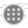
- FIG. 2 is a horizontal sectional view of the susceptor 217 and shows a horizontal section at a position where the reflector 219 is provided.
- the reflector 219 is provided so as to be stored in a space provided inside the susceptor 217. Further, in order to support the space in which the reflector 219 is stored, an outer peripheral portion 217A is provided on the outer periphery of the circular susceptor 217, and a plurality of columnar portions 217B are provided on the inner side.
- a gap is provided between the reflector 219, the outer peripheral portion 217A, and the columnar portion 217B so as not to contact and damage the outer peripheral portion 217A or the columnar portion 217B. 222 is provided.
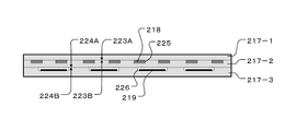
- FIG. 3 is a vertical sectional view showing structures of the susceptor 217, the heater 218, and the reflector 219 according to the comparative example, and shows a cross section in the vertical direction along the one-dot chain line AA ′ in FIG.
- the susceptor 217 is configured by laminating an upper quartz plate 217-1, a middle quartz plate 217-2, and a lower quartz plate 217-3 in order from the top.
- the wafer 200 is placed directly on the upper surface of the upper quartz plate 217-1 or via a susceptor cover or the like.
- the upper quartz plate 217-1 and the middle quartz plate 217-2 are bonded to the bonding surface 223A formed on the lower surface of the upper quartz plate 217-1 and the bonding surface 223B formed on the upper surface of the middle quartz plate 217-2. Are joined.
- the middle quartz plate 217-2 and the lower quartz plate 217-3 are bonded to the bonding surface 224A formed on the lower surface of the middle quartz plate 217-2 and the bonding surface 224B formed on the upper surface of the lower quartz plate 217-3. Are joined.
- a heater storage portion 225 which is a space in which the heater 218 is stored, is formed.
- the heater 218 is housed in the heater housing 225, and the upper quartz plate 217-1 and the middle quartz plate 217-2 are bonded together, so that the heater 218 is sealed between the two plates. Since the heater 218 is sealed in the susceptor 217, the heater 218 is not in contact with the gas in the processing chamber 201.
- the heater storage portion 225 is formed in a groove shape or the like according to the shape of the heater 218, for example. However, the shape is not limited to the groove shape, and various shapes can be formed on the middle quartz plate 217-2 according to the shape of the heater 218. It can form as a recessed part.
- the lower quartz plate 217-3 is formed with a reflector storage portion 226 that is a space in which the reflector 219 is stored.
- the reflector 219 is stored in the reflector storage unit 226, and the middle quartz plate 217-2 and the lower quartz plate 217-3 are bonded together, so that the reflector 219 is sealed between both plates. Since the reflector 219 is sealed in the susceptor 217 in a vacuum state, the reflector 219 does not come into contact with the gas in the processing chamber 201.
- the reflector storage portion 226 is formed in the lower quartz plate 217-3 as a recess that matches the shape of the reflector 219 shown in FIG.
- the susceptor 217 since the susceptor 217 has a structure formed of quartz having a columnar portion 217B and the like inside, the upper quartz plate 217-1 is formed by using a welding technique like a susceptor formed of aluminum, stainless steel, or the like. It is generally difficult to bond the middle quartz plate 217-2 and the lower quartz plate 217-3. Therefore, these quartz plates are bonded to each other using a thermocompression bonding technique.
- the thermocompression bonding is performed, for example, by pressing the bonded surfaces of these quartz plates to each other with a predetermined pressure for a predetermined time at a high temperature at which the viscosity of the quartz is reduced.
- the bonding surfaces 223A, 223B, 224A, and 224B are , For example, by polishing, so as to be a transparent and flat surface. Specifically, the entire adhesive surface 223A, the surface excluding the portion of the adhesive surface 223B where the heater accommodating portion 225 is formed, the entire adhesive surface 224A, and the reflector storage portion 226 of the adhesive surface 224B are formed. The surface excluding the portion (that is, the portion corresponding to the outer peripheral portion 217A and the columnar portion 217B) is processed to be a transparent and flat surface.
- the adhesive surfaces 223A, 223B, 224A, and 224B are formed and thermocompression bonded as in the comparative example, there are the following problems that occur when the reflector 219 expands and deforms due to heat.
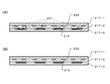
- FIG. 4A is a vertical cross-sectional view of the susceptor 217 and the like showing the state of the reflector 219 during the thermocompression bonding process in the comparative example.
- the quartz plate is heated to a temperature at which the viscosity of the quartz becomes small.
- the reflector 219 made of a metal material is also heated, and the metal material causes thermal expansion.
- the reflector 219 is deformed due to a difference in temperature distribution. For example, as shown in FIG. May be in contact with the adhesive surface 224A.
- the metal material of the reflector 219 expands greatly, so that contact due to deformation is likely to occur.
- a broken line circle in FIG. 4A indicates a contact portion 227.
- a part of the reflector 219 that has contacted the bonding surface 224A is in close contact with the bonding surface 224A, which is a transparent and flat surface. It may be attached.
- FIG. 4B is a vertical sectional view of the susceptor 217, the heater 218, and the reflector 219 showing the state of the reflector 219 when the susceptor 217 is cooled after the thermocompression bonding process in the comparative example.
- the reflector 219 contracts to return to the original shape.
- FIG. 4A when a part of the reflector 219 sticks to the bonding surface 224A, a force to move away from the bonding surface 224A acts on the sticking portion.
- FIG. 4A when a part of the reflector 219 sticks to the bonding surface 224A, a force to move away from the bonding surface 224A acts on the sticking portion.
- the surface of the adhesive surface 224A may be peeled off together with the portion where the reflector 219 is attached, and a crack may be generated on the surface of the adhesive surface 224A.
- the broken-line circle in FIG. 4B shows a crack occurrence location 228.
- the reflector 219 does not return to its original shape after cooling, and is deformed. Sometimes it will remain.
- the depth of the reflector storage portion 226 it is conceivable to increase the depth of the reflector storage portion 226 so that the reflector 219 does not contact the bonding surface 224A in the thermocompression bonding step.
- the columnar portion 217B is thickened so that the susceptor 217 has strength (vacuum resistance strength) to withstand stress applied when the processing chamber 201 is evacuated.
- the number of reflectors 219 that can be installed is reduced. As a result, the area for reflecting the radiant heat from the heater 218 is reduced, and the efficiency and uniformity of heating by the heater 218 are deteriorated. Therefore, it is desirable to solve the above-mentioned problem without increasing the depth of the reflector storage unit 226.
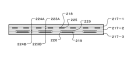
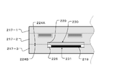
- a reflector facing recess 229 is provided on the lower surface of the middle quartz plate 217-2 in the susceptor 217 and facing the reflector storage portion 226.
- the ceiling surface of the reflector facing recess 229 (the surface facing the reflector storage unit 226) is subjected to a roughening process having a surface roughness of a predetermined level or more.
- the roughened ceiling surface is shown as a rough ceiling surface 230.
- the surface roughness of the ceiling rough surface 230 is greater than the surface roughness of at least the transparent and flat surface of the bonding surface 224A. Therefore, as will be described later, compared to the comparative example, the reflector 219 can be prevented from sticking to the lower surface of the middle quartz plate 217-2 during the thermocompression bonding.
- the reflector facing recess 229 can be formed by grinding the polished bonding surface 224A before the thermocompression bonding step. At this time, a rough surface generated on the inner wall surface of the reflector facing recess 229 by grinding can be used as the ceiling rough surface 230 as it is. Further, since the rough ceiling surface 230 is formed inside the reflector facing recess 229, even after the reflector facing recess 229 is formed, the lower surface of the middle quartz plate 217-2 is left with the ceiling rough surface 230 remaining.
- the adhesive surface 224A can be formed by polishing. Note that the ceiling rough surface 230 may be formed by other roughening processing techniques such as physical processing such as sand blasting or heat treatment, or chemical processing using hydrogen fluoride.
- the bottom surface of the reflector storage unit 226 (the surface on which the reflector 219 is placed) may be subjected to a roughening process having a surface roughness of a predetermined level or more.
- the roughened bottom surface is shown as a bottom rough surface 231.
- the surface roughness of the bottom rough surface 231 may be the same as that of the ceiling rough surface 230, and may be appropriately selected within the range of the surface roughness values of the ceiling rough surface 230 described above.
- the reflector housing 226 can be formed by grinding the upper surface of the lower quartz plate 217-3 prior to the thermocompression bonding step.
- the rough surface generated on the inner wall surface can be used as the bottom rough surface 231 as it is.
- the polishing process for forming the bonding surface 224B may be performed either before or after the reflector storage portion 226 is formed.
- the rough bottom surface 231 may be formed by another roughening technique.
- FIG. 7A is a vertical cross-sectional view of the susceptor 217 and the like showing the state of the reflector 219 during the thermocompression bonding process in this embodiment.
- FIG. 7B is a vertical cross-sectional view showing the state of the reflector 219 when the susceptor 217 is cooled after the thermocompression bonding step in this embodiment.
- the reflector 219 heated by thermocompression bonding is deformed due to thermal expansion, and a part of the reflector 219 contacts the rough ceiling surface 230, for example, like a contact location 227 shown in FIG. There is a case.
- the contact portion 227 is a roughened surface (ceiling rough surface 230). Therefore, sticking of the reflector 219 can be suppressed as compared with the case where it comes into contact with the adhesive surface 224A which is a transparent and flat surface. Therefore, as shown in FIG. 7B, even if the reflector 219 returns to its original shape after cooling, the lower surface of the middle quartz plate 217-2 caused by sticking of the reflector 219 does not peel off or crack. Can be. Further, it is possible to reduce a problem that the reflector 219 does not return to its original shape while sticking after cooling.
- the reflector 219 can be prevented from sticking to the bottom surface of the reflector storage portion 226 during the thermocompression bonding process. It is possible to reduce problems such as peeling of the surface on the bottom surface of the reflector storage portion 226 after cooling, or returning of the reflector 219 while it is deformed.
- the reflector is stored so that such contact does not occur. It is not necessary to ensure a large depth of the portion 226. Therefore, the depth of the reflector storage portion 226 can be made smaller than before, so that the vacuum resistance of the susceptor 217 can be improved, and the susceptor 217 can be made thinner.
- the depth of the reflector facing recess 229 is preferably small from the viewpoint of vacuum resistance. In this embodiment, for example, the thickness is set to 0.2 to 0.4 mm in consideration of processing accuracy.
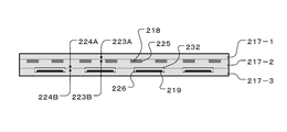
- FIG. 8 is a vertical sectional view showing the structures of the susceptor 217, the heater 218, and the reflector 219 according to the present embodiment, and shows a vertical section taken along one-dot chain line AA ′ in FIG.
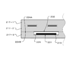
- FIG. 9 is an enlarged cross-sectional view in which a part of FIG. 8 is enlarged.
- symbol as 1st Embodiment or a comparative example is attached
- This embodiment is a modification of the above-described first embodiment, and the reflector facing recess 229 in the first embodiment is not provided.
- the lower surface of the middle quartz plate 217-2 and the portion facing the reflector storage portion 226 is subjected to a roughening process having a surface roughness of a predetermined level or more.
- the lower surface of the roughened middle quartz plate 217-2 is shown as the upper rough surface 232.
- the surface roughness of the upper rough surface 232 is the same as that of the ceiling rough surface 230 in the first embodiment. That is, the surface roughness of the ceiling rough surface 230 is greater than the surface roughness of at least the transparent and flat surface of the bonding surface 224A. Therefore, it is possible to prevent the reflector 219 from sticking to the lower surface of the middle quartz plate 217-2 during the thermocompression bonding. In order to more reliably prevent the reflector 219 from sticking, it is desirable that the surface roughness of the upper rough surface 232 be Ra ⁇ 0.1 ⁇ m.
- the reflector facing recess 229 is not provided as in the first embodiment. Therefore, in order to form the upper rough surface 232, for example, sandblasting or heat treatment or the like is performed on the portion of the bonding surface 224A that has been polished and opposed to the reflector storage portion 226 before the thermocompression bonding step. It is preferable to use a means capable of performing a partial roughening process such as a general process or a chemical process using hydrogen fluoride. However, other methods such as forming the adhesive surface 224A by first forming the upper rough surface 232 and then polishing the lower surface of the middle quartz plate 217-2 leaving only that surface may be used.
- the vacuum resistance strength of the susceptor 217 can be further improved than in the first embodiment, and the susceptor 217 can be further improved. It can also be formed thin.
- the invention according to the present application can also be applied to other processes.
- the present invention can be applied to an apparatus for supplying a source gas and a reactive gas to form a film on a substrate, or performing a substrate process such as a heat treatment, an annealing process, an ashing process, or an etching process.
- Substrate processing apparatus 200 ... wafer, 201 ... processing chamber, 217 ... susceptor, 218 ... heater, 219: Reflector, 221 ... Controller
Landscapes
- Physics & Mathematics (AREA)
- Engineering & Computer Science (AREA)
- Plasma & Fusion (AREA)
- Chemical & Material Sciences (AREA)
- Analytical Chemistry (AREA)
- Container, Conveyance, Adherence, Positioning, Of Wafer (AREA)
- Health & Medical Sciences (AREA)
- Toxicology (AREA)
Abstract
Description
まず、第1の実施形態で好適に使用される基板処理装置について説明する。この基板処理装置は、半導体装置の製造に使用される半導体製造装置の一例として構成されているものである。
処理室201の底側中央には、ウエハ200を載置する基板支持部(基板載置部)としてのサセプタ217が配置されている。サセプタ217は、ヒータ218とリフレクタ(反射部材)219を内蔵しており、非金属材料の部材により構成されている。本実施形態では石英で形成されている。また、サセプタ217とウエハ200との間には、サセプタ217側からの熱をウエハ200へ均一に伝えるためのサセプタカバーを設けることもできる。サセプタカバーは、窒化アルミニウム(AlN)、セラミックス、石英、炭化ケイ素(SiC)等の非金属材料から形成されている。
処理室201の上方、つまり上側容器210の上部には、シャワーヘッド236が設けられている。シャワーヘッド236は、キャップ状の蓋体233と、ガス導入口234と、バッファ室237と、開口238と、遮蔽プレート240と、ガス吹出口239とを備え、反応ガスを処理室201内へ供給できるように構成されている。バッファ室237は、ガス導入口234より導入される反応ガスを分散する分散空間としての機能を持つ。
下側容器211の側壁には、処理室201内から反応ガスを排気するガス排気口235が設けられている。ガス排気口235には、ガス排気管231の上流端が接続されている。ガス排気管231には、上流側から順に圧力調整器(圧力調整部)としてのAPC(Auto Pressure Controller)242、開閉弁としてのバルブ243B、真空排気装置としての真空ポンプ246が設けられている。
処理室201の外周部、すなわち上側容器210の側壁の外側には、処理室201を囲うように、螺旋状の共振コイル212が設けられている。共振コイル212には、RFセンサ272、高周波電源273と周波数整合器274が接続される。高周波電源273は、共振コイル212に高周波電力を供給するものである。RFセンサ272は高周波電源273の出力側に設けられている。RFセンサ272は、供給される高周波の進行波や反射波の情報をモニタするものである。周波数整合器274は、RFセンサ272でモニタされた反射波の情報に基づいて、反射波が最小となるよう、高周波電源273を制御するものである。
制御部としてのコントローラ221は、信号線Aを通じてAPC242、バルブ243Bおよび真空ポンプ246を、信号線Bを通じてサセプタ昇降機構268を、信号線Cを通じてヒータ275を、信号線Dを通じてゲートバルブ244を、信号線Eを通じてRFセンサ272、高周波電源273および周波数整合器274を、信号線Fを通じてマスフローコントローラ252A,252B,252Cおよびバルブ253A,253B,253C,243Aを、各々制御するように構成されている。
次に、第1の実施形態において好適に実施される基板処理工程について説明する。本実施形態に係る基板処理工程は、例えばフラッシュメモリ等の半導体デバイスの製造工程の一工程として、上述の基板処理装置100により実施される。なお以下の説明において、基板処理装置100を構成する各部の動作は、コントローラ221により制御される。
まず、ウエハ200を処理室201内に搬入する。具体的には、サセプタ昇降機構268がウエハ200の搬送位置までサセプタ217を下降させて、サセプタ217の貫通孔220にウエハ突上げピン266を貫通させる。その結果、ウエハ突き上げピン266が、サセプタ217表面よりも所定の高さ分だけ突出した状態となる。
続いて、処理室201内に搬入されたウエハ200の昇温を行う。ヒータ218は予め加熱されており、ヒータ218が内蔵されたサセプタ217上に、搬入されたウエハ200を保持することで、例えば150℃以上650℃以下の範囲内の所定値にウエハ200を加熱する。また、ウエハ200の昇温を行う間、真空ポンプ246によりガス排気口235を介して処理室201内を真空排気し、処理室201内の圧力を0.1Pa以上1000Pa以下の範囲内の所定値とする。真空ポンプ246は、少なくとも後述の基板搬出工程が終了するまで作動させておく。
次に、反応ガスとしての酸素ガスの供給を開始する。具体的には、バルブ253Aを開け、マスフローコントローラ252Aにて流量制御しながら、バッファ室237を介して処理室201内への酸素ガスの供給を開始する。このとき、酸素ガスの流量を、例えば100sccm以上1000sccm以下の範囲内の所定値とする。また、処理室201内の圧力が、例えば1Pa以上1000Pa以下の範囲内の所定圧力となるように、APC242の開度を調整して処理室201内を排気する。このように、処理室201内を適度に排気しつつ、後述のプラズマ処理工程の終了時まで酸素ガスの供給を継続する。
処理室201内の圧力が安定したら、共振コイル212に対して高周波電源273から整合器272を介して、高周波電力の印加を開始する。
所定の処理時間が経過して酸素ガスの供給を停止したら、ガス排気口235を介して処理室201内を真空排気する。これにより、処理室201内の酸素ガスや、酸素ガスが反応した排ガス等を処理室201外へと排気する。その後、APC242の開度を調整し、処理室201内の圧力を処理室201に隣接する真空搬送室(ウエハ200の搬出先。図示せず)と同じ圧力(例えば100Pa)に調整する。
処理室201内が所定の圧力となったら、サセプタ217をウエハ200の搬送位置まで下降させ、ウエハ突上げピン266上にウエハ200を支持させる。そして、ゲートバルブ244を開き、図中省略の搬送機構を用いてウエハ200を処理室201外へ搬出する。以上により、本実施形態に係る基板処理工程を終了する。
続いて第1の実施形態におけるサセプタ217、ヒータ218およびリフレクタ219の構造について、比較例と比較しながら説明する。
図3は、比較例に係るサセプタ217、ヒータ218及びリフレクタ219の構造を示す垂直断面図であり、図2における一点鎖線A-A´における垂直方向の断面を示している。
続いて上述の比較例に対する第1の実施形態について図5、図6及び図7(A)(B)を用いて説明する。図5は、本実施形態に係るサセプタ217、ヒータ218及びリフレクタ219の構造を示す垂直断面図であり、図2における一点鎖線A-A´における垂直方向の断面を示している。図6は、図5の一部を拡大した拡大断面図である。なお、比較例と同一の構成には比較例と同一の符号を付している。
続いて第2の実施形態について図8および図9を用いて説明する。図8は、本実施形態に係るサセプタ217、ヒータ218及びリフレクタ219の構造を示す垂直断面図であり、図2における一点鎖線A-A´における垂直方向の断面を示している。図9は、図8の一部を拡大した拡大断面図である。なお、第1の実施形態又は比較例と同一の構成には第1の実施形態又は比較例と同一の符号を付している。
200・・・ウエハ、
201・・・処理室、
217・・・サセプタ、
218・・・ヒータ、
219・・・リフレクタ、
221・・・コントローラ
Claims (17)
- 基板が上部に載置される、石英で構成された上側サセプタと、
石英で構成された下側サセプタと、
面状に形成された金属により構成された熱を反射するリフレクタと、を有し、
前記上側サセプタの下面と前記下側サセプタの上面は、その間に前記リフレクタを挟むように接着されており、
前記下側サセプタの上面には、前記リフレクタを収容する第1の凹部が形成されており、
前記上側サセプタの下面であって前記第1の凹部に対向する部分は表面を粗面化する加工が施されている基板支持台。 - 請求項1に記載の基板支持台であって、
前記上側サセプタの内部には熱を放射する発熱素子が設けられ、
前記リフレクタは、前記発熱素子から放射される熱を反射するよう構成されている。 - 請求項2に記載の基板支持台であって、
前記上側サセプタは、
前記基板が上部に載置される上部プレートと、
前記下側サセプタと接着される下部プレートと、
前記上部プレートと前記下部プレートの間に挟まれるように設けられる前記発熱素子と、を有する。 - 請求項1に記載の基板支持台であって、
前記上側サセプタと前記下側サセプタは、研磨加工された前記上側サセプタの下面と前記下側サセプタの上面を加熱圧着することにより接着されており、
前記上側サセプタの下面であって前記第1の凹部に対向する部分の表面粗さは、研磨加工された前記上側サセプタの下面の表面粗さよりも大きい。 - 請求項1に記載の基板支持台であって、
前記上側サセプタの下面であって前記第1の凹部に対向する部分の表面粗さは0.1μm以上である。 - 請求項1に記載の基板支持台であって、
前記上側サセプタの下面であって前記第1の凹部に対向する部分には第2の凹部が形成され、前記第2の凹部の内面であって前記第1の凹部に対向する部分は粗面化されている。 - 請求項6に記載の基板支持台であって、前記第2の凹部及び前記第2の凹部の内面であって前記第1の凹部に対向する粗面化された面は、研削加工により形成される。
- 請求項1に記載の基板支持台であって、
前記第1の凹部の底面は粗面化されている。 - 請求項8に記載の基板支持台であって、
前記上側サセプタと前記下側サセプタは、
研磨加工された前記上側サセプタの下面と前記下側サセプタの上面を加熱圧着することにより接着されており、
前記第1の凹部の底面の表面粗さは、研磨加工された前記下側サセプタの上面の表面粗さよりも大きい。 - 請求項8に記載の基板支持台であって、
前記第1の凹部及び前記第1の凹部の粗面化された底面は、研削加工により形成される。 - 請求項8に記載の基板支持台であって、
前記上側サセプタの下面であって前記第1の凹部に対向する部分の表面粗さは、前記第1の凹部の底面の表面粗さと実質的に同一である。 - 請求項1に記載の基板支持台であって、
前記上側サセプタの下面であって前記第1の凹部に対向する部分と、前記上側サセプタの下面であって前記下側サセプタと接着された接着面は同一平面を成している。 - 請求項12に記載の基板支持台であって、
前記上側サセプタと前記下側サセプタは、研磨加工された前記上側サセプタの下面と前記下側サセプタの上面を加熱圧着することにより接着されており、
前記上側サセプタの下面であって前記第1の凹部に対向する部分の表面粗さは、研磨加工された前記上側サセプタの下面の表面粗さよりも大きい。 - 請求項12に記載の基板支持台であって、
前記上側サセプタの下面であって前記第1の凹部に対向する部分の表面粗さは0.1μm以上である。 - 請求項1に記載の基板支持台であって、
前記リフレクタはモリブデン又はタングステンにより構成される。 - 基板が載置される基板支持台を備える基板処理装置であって、
前記基板支持台は、
前記基板が上部に載置される、石英で構成された上側サセプタと、
前記上側サセプタの内部又は前記上側サセプタと前記基板との間に設けられた熱を放射する発熱素子と、
石英で構成された下側サセプタと、面状に形成された金属により構成された、前記発熱素子から放射される熱を反射するリフレクタと、を有し、
前記上側サセプタの下面と前記下側サセプタの上面は、その間に前記リフレクタを挟むように接着されており、
前記下側サセプタの上面には、前記リフレクタを収容する第1の凹部が形成されており、
前記上側サセプタの下面であって前記第1の凹部に対向する部分は表面を粗面化する加工が施されている。 - 基板支持台の上面に基板を載置する工程と、
前記基板支持台の上面に載置された前記基板を加熱する工程と、を有する半導体装置の製造方法であって、
前記基板支持台は、
前記基板が上部に載置される、石英で構成された上側サセプタと、
石英で構成された下側サセプタと、
面状に形成された金属により構成された熱を反射するリフレクタと、を有し、
前記上側サセプタの下面と前記下側サセプタの上面は、その間に前記リフレクタを挟むように接着されており、
前記下側サセプタの上面には、前記リフレクタを収容する第1の凹部が形成されており、
前記上側サセプタの下面であって前記第1の凹部に対向する部分は表面を粗面化する加工が施されている、
半導体装置の製造方法。
Priority Applications (4)
| Application Number | Priority Date | Filing Date | Title |
|---|---|---|---|
| PCT/JP2016/059675 WO2017163409A1 (ja) | 2016-03-25 | 2016-03-25 | 基板支持台、基板処理装置および半導体装置の製造方法 |
| JP2018506731A JP6521475B2 (ja) | 2016-03-25 | 2016-03-25 | 基板支持台、基板処理装置および半導体装置の製造方法 |
| KR1020187024855A KR102193326B1 (ko) | 2016-03-25 | 2016-03-25 | 기판 지지대, 기판 처리 장치 및 반도체 장치의 제조 방법 |
| US16/117,328 US11211280B2 (en) | 2016-03-25 | 2018-08-30 | Substrate support and substrate processing apparatus |
Applications Claiming Priority (1)
| Application Number | Priority Date | Filing Date | Title |
|---|---|---|---|
| PCT/JP2016/059675 WO2017163409A1 (ja) | 2016-03-25 | 2016-03-25 | 基板支持台、基板処理装置および半導体装置の製造方法 |
Related Child Applications (1)
| Application Number | Title | Priority Date | Filing Date |
|---|---|---|---|
| US16/117,328 Continuation US11211280B2 (en) | 2016-03-25 | 2018-08-30 | Substrate support and substrate processing apparatus |
Publications (1)
| Publication Number | Publication Date |
|---|---|
| WO2017163409A1 true WO2017163409A1 (ja) | 2017-09-28 |
Family
ID=59900129
Family Applications (1)
| Application Number | Title | Priority Date | Filing Date |
|---|---|---|---|
| PCT/JP2016/059675 Ceased WO2017163409A1 (ja) | 2016-03-25 | 2016-03-25 | 基板支持台、基板処理装置および半導体装置の製造方法 |
Country Status (4)
| Country | Link |
|---|---|
| US (1) | US11211280B2 (ja) |
| JP (1) | JP6521475B2 (ja) |
| KR (1) | KR102193326B1 (ja) |
| WO (1) | WO2017163409A1 (ja) |
Cited By (5)
| Publication number | Priority date | Publication date | Assignee | Title |
|---|---|---|---|---|
| WO2020171179A1 (ja) * | 2019-02-21 | 2020-08-27 | 京セラ株式会社 | 試料保持具 |
| JPWO2021039497A1 (ja) * | 2019-08-29 | 2021-03-04 | ||
| WO2021193473A1 (ja) * | 2020-03-25 | 2021-09-30 | 株式会社Kokusai Electric | 基板処理装置、基板載置台カバー及び半導体装置の製造方法 |
| US20220139760A1 (en) * | 2019-09-17 | 2022-05-05 | Kokusai Electric Corporation | Substrate processing apparatus, susceptor cover, method of manufacturing semiconductor device and substrate processing method |
| WO2023090266A1 (ja) * | 2021-11-19 | 2023-05-25 | 日本電産サンキョー株式会社 | レンズユニット |
Families Citing this family (1)
| Publication number | Priority date | Publication date | Assignee | Title |
|---|---|---|---|---|
| JP7230679B2 (ja) * | 2019-05-15 | 2023-03-01 | 住友電気工業株式会社 | 半導体素子の製造方法 |
Citations (4)
| Publication number | Priority date | Publication date | Assignee | Title |
|---|---|---|---|---|
| WO2004095560A1 (ja) * | 2003-04-18 | 2004-11-04 | Hitachi Kokusai Electric Inc. | 半導体製造装置および半導体装置の製造方法 |
| JP2007042958A (ja) * | 2005-08-05 | 2007-02-15 | Sumitomo Electric Ind Ltd | ウェハプローバ用ウェハ保持体およびそれを搭載したウェハプローバ |
| JP2007258585A (ja) * | 2006-03-24 | 2007-10-04 | Tokyo Electron Ltd | 基板載置機構および基板処理装置 |
| JP2011119326A (ja) * | 2009-12-01 | 2011-06-16 | Tokyo Electron Ltd | 基板載置台、その製造方法及び基板処理装置 |
Family Cites Families (2)
| Publication number | Priority date | Publication date | Assignee | Title |
|---|---|---|---|---|
| US8961691B2 (en) * | 2008-09-04 | 2015-02-24 | Tokyo Electron Limited | Film deposition apparatus, film deposition method, computer readable storage medium for storing a program causing the apparatus to perform the method |
| KR101205433B1 (ko) * | 2010-07-28 | 2012-11-28 | 국제엘렉트릭코리아 주식회사 | 기판 서셉터 및 그것을 갖는 증착 장치 |
-
2016
- 2016-03-25 WO PCT/JP2016/059675 patent/WO2017163409A1/ja not_active Ceased
- 2016-03-25 KR KR1020187024855A patent/KR102193326B1/ko active Active
- 2016-03-25 JP JP2018506731A patent/JP6521475B2/ja active Active
-
2018
- 2018-08-30 US US16/117,328 patent/US11211280B2/en active Active
Patent Citations (4)
| Publication number | Priority date | Publication date | Assignee | Title |
|---|---|---|---|---|
| WO2004095560A1 (ja) * | 2003-04-18 | 2004-11-04 | Hitachi Kokusai Electric Inc. | 半導体製造装置および半導体装置の製造方法 |
| JP2007042958A (ja) * | 2005-08-05 | 2007-02-15 | Sumitomo Electric Ind Ltd | ウェハプローバ用ウェハ保持体およびそれを搭載したウェハプローバ |
| JP2007258585A (ja) * | 2006-03-24 | 2007-10-04 | Tokyo Electron Ltd | 基板載置機構および基板処理装置 |
| JP2011119326A (ja) * | 2009-12-01 | 2011-06-16 | Tokyo Electron Ltd | 基板載置台、その製造方法及び基板処理装置 |
Cited By (14)
| Publication number | Priority date | Publication date | Assignee | Title |
|---|---|---|---|---|
| JPWO2020171179A1 (ja) * | 2019-02-21 | 2021-12-09 | 京セラ株式会社 | 試料保持具 |
| KR20210109609A (ko) * | 2019-02-21 | 2021-09-06 | 교세라 가부시키가이샤 | 시료 유지구 |
| WO2020171179A1 (ja) * | 2019-02-21 | 2020-08-27 | 京セラ株式会社 | 試料保持具 |
| JP7116241B2 (ja) | 2019-02-21 | 2022-08-09 | 京セラ株式会社 | 試料保持具 |
| KR102611059B1 (ko) | 2019-02-21 | 2023-12-07 | 교세라 가부시키가이샤 | 시료 유지구 |
| JPWO2021039497A1 (ja) * | 2019-08-29 | 2021-03-04 | ||
| WO2021039497A1 (ja) * | 2019-08-29 | 2021-03-04 | 京セラ株式会社 | 基体構造体及び基体構造体を用いた対象物載置装置 |
| US20220139760A1 (en) * | 2019-09-17 | 2022-05-05 | Kokusai Electric Corporation | Substrate processing apparatus, susceptor cover, method of manufacturing semiconductor device and substrate processing method |
| WO2021193473A1 (ja) * | 2020-03-25 | 2021-09-30 | 株式会社Kokusai Electric | 基板処理装置、基板載置台カバー及び半導体装置の製造方法 |
| JP7297149B2 (ja) | 2020-03-25 | 2023-06-23 | 株式会社Kokusai Electric | 基板処理装置、基板載置台カバー、半導体装置の製造方法及びプログラム |
| JPWO2021193473A1 (ja) * | 2020-03-25 | 2021-09-30 | ||
| WO2023090266A1 (ja) * | 2021-11-19 | 2023-05-25 | 日本電産サンキョー株式会社 | レンズユニット |
| JP2023075470A (ja) * | 2021-11-19 | 2023-05-31 | ニデックインスツルメンツ株式会社 | レンズユニット |
| JP7798541B2 (ja) | 2021-11-19 | 2026-01-14 | ニデックインスツルメンツ株式会社 | レンズユニット |
Also Published As
| Publication number | Publication date |
|---|---|
| US11211280B2 (en) | 2021-12-28 |
| JPWO2017163409A1 (ja) | 2018-12-06 |
| KR102193326B1 (ko) | 2020-12-22 |
| KR20180107196A (ko) | 2018-10-01 |
| JP6521475B2 (ja) | 2019-05-29 |
| US20180374740A1 (en) | 2018-12-27 |
Similar Documents
| Publication | Publication Date | Title |
|---|---|---|
| JP6521475B2 (ja) | 基板支持台、基板処理装置および半導体装置の製造方法 | |
| CN106558517B (zh) | 衬底处理装置及半导体器件的制造方法 | |
| JP6270952B1 (ja) | 基板処理装置、半導体装置の製造方法および記録媒体。 | |
| JP6318139B2 (ja) | 基板処理装置、半導体装置の製造方法及びプログラム | |
| JP4067858B2 (ja) | Ald成膜装置およびald成膜方法 | |
| JP5885404B2 (ja) | 基板処理装置及び半導体装置の製造方法 | |
| JP4732351B2 (ja) | 処理装置及びヒーターユニット | |
| JP5876992B2 (ja) | プラズマ処理装置 | |
| JP5320171B2 (ja) | 基板処理装置 | |
| CN113614892B (zh) | 基板处理装置、处理容器、反射体和半导体装置的制造方法 | |
| WO2004095560A1 (ja) | 半導体製造装置および半導体装置の製造方法 | |
| TWI425112B (zh) | A substrate mounting mechanism, and a substrate processing device including the substrate mounting mechanism | |
| US20220139760A1 (en) | Substrate processing apparatus, susceptor cover, method of manufacturing semiconductor device and substrate processing method | |
| JP5465828B2 (ja) | 基板処理装置及び半導体デバイスの製造方法 | |
| JP2012054399A (ja) | 半導体製造装置及び半導体製造方法 | |
| US20220415700A1 (en) | Substrate processing apparatus, substrate mounting table cover, method of manufacturing semiconductor device and non-transitory computer readable recording medium | |
| JP2011091389A (ja) | 基板処理装置及び半導体装置の製造方法 | |
| CN100561680C (zh) | 等离子体处理装置、等离子体处理装置内用的处理容器以及电介质板 | |
| US7527706B2 (en) | Plasma processing apparatus, process vessel for plasma processing apparatus and dielectric plate for plasma processing apparatus | |
| TW202331887A (zh) | 基板處理裝置、半導體裝置之製造方法及程式 | |
| WO2016056338A1 (ja) | 基板処理装置、基板載置台および半導体装置の製造方法 | |
| KR20220015449A (ko) | 반도체 장치의 제조 방법 및 제조 장치 | |
| JP2005260251A (ja) | 載置台、プラズマ処理装置、および載置台の製造方法 | |
| JP4578232B2 (ja) | 半導体製造装置及び半導体製造方法 | |
| CN121885497A (zh) | 基板处理装置、保护部件、半导体器件的制造方法及程序产品 |
Legal Events
| Date | Code | Title | Description |
|---|---|---|---|
| WWE | Wipo information: entry into national phase |
Ref document number: 2018506731 Country of ref document: JP |
|
| ENP | Entry into the national phase |
Ref document number: 20187024855 Country of ref document: KR Kind code of ref document: A |
|
| WWE | Wipo information: entry into national phase |
Ref document number: 1020187024855 Country of ref document: KR |
|
| NENP | Non-entry into the national phase |
Ref country code: DE |
|
| 121 | Ep: the epo has been informed by wipo that ep was designated in this application |
Ref document number: 16895440 Country of ref document: EP Kind code of ref document: A1 |
|
| 122 | Ep: pct application non-entry in european phase |
Ref document number: 16895440 Country of ref document: EP Kind code of ref document: A1 |