WO2017160045A1 - 미세패턴전극 - Google Patents
미세패턴전극 Download PDFInfo
- Publication number
- WO2017160045A1 WO2017160045A1 PCT/KR2017/002713 KR2017002713W WO2017160045A1 WO 2017160045 A1 WO2017160045 A1 WO 2017160045A1 KR 2017002713 W KR2017002713 W KR 2017002713W WO 2017160045 A1 WO2017160045 A1 WO 2017160045A1
- Authority
- WO
- WIPO (PCT)
- Prior art keywords
- pattern
- composition
- line width
- substrate
- value
- Prior art date
- Legal status (The legal status is an assumption and is not a legal conclusion. Google has not performed a legal analysis and makes no representation as to the accuracy of the status listed.)
- Ceased
Links
Images

Classifications
-
- B—PERFORMING OPERATIONS; TRANSPORTING
- B41—PRINTING; LINING MACHINES; TYPEWRITERS; STAMPS
- B41M—PRINTING, DUPLICATING, MARKING, OR COPYING PROCESSES; COLOUR PRINTING
- B41M1/00—Inking and printing with a printer's forme
- B41M1/12—Stencil printing; Silk-screen printing
-
- H—ELECTRICITY
- H01—ELECTRIC ELEMENTS
- H01B—CABLES; CONDUCTORS; INSULATORS; SELECTION OF MATERIALS FOR THEIR CONDUCTIVE, INSULATING OR DIELECTRIC PROPERTIES
- H01B1/00—Conductors or conductive bodies characterised by the conductive materials; Selection of materials as conductors
- H01B1/06—Conductors or conductive bodies characterised by the conductive materials; Selection of materials as conductors mainly consisting of other non-metallic substances
- H01B1/12—Conductors or conductive bodies characterised by the conductive materials; Selection of materials as conductors mainly consisting of other non-metallic substances organic substances
-
- H—ELECTRICITY
- H01—ELECTRIC ELEMENTS
- H01B—CABLES; CONDUCTORS; INSULATORS; SELECTION OF MATERIALS FOR THEIR CONDUCTIVE, INSULATING OR DIELECTRIC PROPERTIES
- H01B13/00—Apparatus or processes specially adapted for manufacturing conductors or cables
-
- H—ELECTRICITY
- H01—ELECTRIC ELEMENTS
- H01B—CABLES; CONDUCTORS; INSULATORS; SELECTION OF MATERIALS FOR THEIR CONDUCTIVE, INSULATING OR DIELECTRIC PROPERTIES
- H01B5/00—Non-insulated conductors or conductive bodies characterised by their form
- H01B5/14—Non-insulated conductors or conductive bodies characterised by their form comprising conductive layers or films on insulating-supports
Definitions
- the present invention relates to a fine pattern electrode, and in particular, to produce a fine pattern electrode and the fine pattern electrode which can greatly improve the reliability and lifespan of electronic components due to excellent precision, straightness, and flatness formed through the screen printing method.
- the present invention relates to a printing pattern measuring instrument for improving straightness, flatness and productivity, and a composition for forming an electrode.
- Corresponding printing methods include offset printing, digital printing, flexo graphic printing, gravure printing, screen printing, and the like.
- the screen printing method which is easy to apply to the process, fixes the screen mesh to the frame, and forms a valve by photochemical method on it to block the portions other than necessary images, and puts the pattern forming composition therein to press the screen to move the pattern forming composition. Is a principle that is printed by being printed on a printed object such as a substrate placed under the plate through the mesh of the part without a plate.
- the screen printing method is preferred to other printing methods because it is easy to adjust the line width of the pattern, printability on various substrates, printing even complex patterns, and the choice of solvents in the industrial field Because the advantages are excellent.
- an object of the present invention is to provide a fine pattern electrode with a fine pattern formed precisely through the screen printing method.
- the present invention measures the presence or absence of abnormality by judging the pattern printed with the paste and the printability of the pattern, and if good, go to the drying process, and if it is poor, erase the printed pattern to recycle the substrate to improve productivity
- An object of the present invention is to provide a printed pattern measuring instrument.
- an object of the present invention is to provide a printing pattern measuring device and a control method thereof for setting parameters for determining accuracy, straightness, and flatness of a finely printed pattern and determining whether the pattern is defective using the same.
- an object of the present invention is to provide a composition for forming an electrode suitable for forming a fine pattern precisely through the printing method.
- ⁇ E LS is an amount of change in the interfacial free energy of the substrate and the printing composition
- ⁇ E AL is an amount of change in the interfacial free energy of the printing composition and the atmosphere
- e * represents a half value of the printed line width
- the ⁇ E total may be calculated as a measurable value as shown in Equation 2 below.
- ⁇ LS is the surface tension [N / m] between the composition and the substrate 400
- ⁇ AL is the surface tension [N / m] between the composition and the atmosphere
- ⁇ means the contact angle [°] between the pattern and the substrate.
- do. e * means half the printed line width.
- ⁇ E A divided by the print area ⁇ E A > ⁇ 1200 (erg / m 2 ) at a printing line width of 10 ⁇ m ⁇ 2e * ⁇ 100 ⁇ m, specifically ⁇ E A > ⁇ 100 (erg / m 2 ).
- R 0 , ⁇ R, R * , q, ⁇ , ⁇ LS , ⁇ AL and ⁇ are the same as defined in Formula 2.
- a printed pattern measuring device that receives an image of a pattern of a printed substrate from a three-dimensional microscope or an optical microscope
- An information receiver configured to receive the image
- a controller configured to analyze the image received from the information receiver to determine whether the pattern is defective and to remove the pattern of the substrate if the pattern is defective;
- the controller may include a calculator configured to analyze an image received from the information receiver to calculate a width and a contact angle of the pattern;
- It includes a defect determination unit for determining whether the pattern is defective by using the width and the contact angle and the surface tension of the pattern,
- the failure determination unit determines whether
- the present invention is a composition for forming an electrode
- the amount of change in interfacial free energy calculated by Equation 1 above ⁇ E total divided by the print area by ⁇ E A is -1200 ⁇ E A ⁇ 0 at a print line width of 10um ⁇ 2e * ⁇ 100um It provides a composition for forming an electrode to be (erg / m 2 ).
- the present invention can provide an electrode in which a fine pattern is precisely formed through a screen printing method, and the electrode according to the present invention can greatly improve the reliability and lifespan of an electronic component due to its excellent precision and accuracy.
- the printing pattern measuring device measures the presence or absence of a pattern printed with a printing paste, and if it is good, moves to a subsequent drying process, and if it is bad, does not dry it, and erases the pattern to recycle the substrate to improve productivity. .
- the printing pattern measuring apparatus can set the parameters for determining the accuracy, straightness, flatness of the fine pattern, it can determine whether the pattern is defective.
- the present invention can provide a composition for forming an electrode suitable for forming an electrode having excellent precision and accuracy through a printing method that can greatly improve the reliability and life of the electronic component.
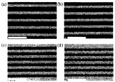
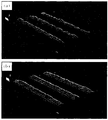
- 1 is an optical microscope image of a pattern printed on a wafer with a line width of 100 um (a), 80 um (b), 50 um (c) and 40 um (d), respectively,
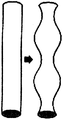
- FIG. 2 is a view showing an example of a normal pattern and a wrinkled pattern
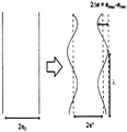
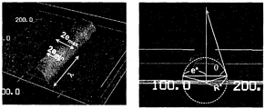
- 3 to 5 are views showing contact angles and line widths
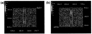
- FIG. 6 is a three-dimensional microscopic image of a pattern printed on a wafer with a line width of 40 um (a) and 80 um (b), respectively,
- FIG. 7 is an optical microscope image of a pattern printed by screen printing a polyimide film (a) without surface treatment and a polyimide film (b) with plasma surface treatment so as to have a line width of 40 um,
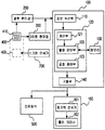
- FIG. 8 is a block diagram of a printing pattern measuring device according to an embodiment of the present invention.
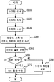
- FIG. 9 is a flowchart illustrating a method of controlling a print pattern measuring device according to an exemplary embodiment of the present invention.
- 1 is an optical microscope image of a pattern printed on a wafer with a line width of 100 um (a), 80 um (b), 50 um (c) and 40 um (d), respectively,
- FIG. 2 is a view showing an example of a normal pattern and a wrinkled pattern
- 3 to 5 are views showing contact angles and line widths
- FIG. 6 is a three-dimensional microscopic image of a pattern printed on a wafer with a line width of 40 um (a) and 80 um (b), respectively,
- FIG. 7 is an optical microscope image of a pattern printed by screen printing a polyimide film (a) without surface treatment and a polyimide film (b) with plasma surface treatment so as to have a line width of 40 um,
- FIG. 8 is a block diagram of a printing pattern measuring device according to an embodiment of the present invention.
- FIG. 9 is a flowchart illustrating a method of controlling a print pattern measuring device according to an exemplary embodiment of the present invention.
- the fine pattern electrode according to the present invention is an electrode formed by the screen printing method
- ⁇ E LS is an amount of change in the interfacial free energy of the substrate and the printing composition
- ⁇ E AL is an amount of change in the interfacial free energy of the printing composition and the atmosphere
- e * represents a half value of the printed line width.
- ⁇ E A may be ⁇ 1200 ⁇ E A ⁇ 300 (erg / m 2 ).
- the ⁇ E total may be calculated as a measurable value as shown in Equation 2 below.
- ⁇ LS is the surface tension [N / m] between the composition and the substrate 400
- ⁇ AL is the surface tension [N / m] between the composition and the atmosphere
- ⁇ means the contact angle [°] between the pattern and the substrate.
- do. e * means half the printed line width.
- ⁇ E A divided by the print area ⁇ E A > ⁇ 1200 (erg / m 2 ) at a printing line width of 10 ⁇ m ⁇ 2e * ⁇ 100 ⁇ m, specifically ⁇ E A > ⁇ 100 (erg / m 2 ).
- the following Formula 3 may be usefully applied.
- R 0 , ⁇ R, R * , q, ⁇ , ⁇ LS , ⁇ AL and ⁇ are the same as defined in Formula 2.
- the interfacial free energy which is the product of the interfacial tension and the surface area, increases, making the whole system unstable.
- the pattern 410 is spontaneously deformed in order to lower the total energy to solve the instability, that is, to reduce the surface area per unit volume. While the volume of the micropattern 410 remains unchanged, to reduce the surface area per unit volume, the possible structures must be united to have a curvature (ie, as much as possible as part of a round sphere). Thus, as observed in c and d of FIG. 1, wrinkles are formed (which were not observed in a and b of FIG. 1).
- the fine pattern 410 when the fine pattern 410 is formed on the substrate 400 by using the paste composition, the sum of the substrate 400 and the paste composition, and the interfacial free energy of the paste composition and the atmosphere is represented by E.
- the difference in interfacial free energy can be expressed by ⁇ E total .
- wrinkles may be reduced according to the specific range of ⁇ E total to ensure accuracy, straightness, and flatness of the fine pattern 410.
- the surface area per unit volume of the pattern 410 becomes large. This can be seen on the same principle that when one cube is divided into several smaller cubes, the surface area versus volume is larger than before dividing.
- the narrower the line width of the printed fine pattern 410 the greater the surface area per unit volume, thereby increasing the interface free energy. Accordingly, in order to lower the total energy of the pattern 410, the pattern 410 spontaneously reduces the surface area, and deformation occurs. At this point, they have curvature and when combined, reduce the surface area per unit volume.
- the printed pattern 410 has a wrinkled shape that is deformed as shown in FIG. 2 in the unwrinkling of the mask pattern.
- the paste pattern 410 may or may not have a wrinkled shape due to factors such as the printing line width, the composition and the surface energy of the substrate 400.
- ⁇ E total is used to determine this.
- the ⁇ E total of the printed paste is
- the correlation between the ⁇ E total value and the final shape of the pattern 410 is as follows.
- the fine pattern 410 when the fine pattern 410 is formed on the substrate 400 through the printing, the amount of change in the interfacial free energy ( ⁇ E LS ) of the substrate 400 and the paste composition and the amount of change in the interfacial free energy of the paste composition and the atmosphere ( ⁇ E AL), the sum ( ⁇ E total) is the value from 0 the more smaller wrinkles (Wrinkling) is generated by precision fine pattern 410 formed of a becomes difficult.
- ⁇ E total is close to 0 (erg) in consideration of the type of substrate 400, the atmosphere, and the like, the accuracy, linearity, and flatness of the fine pattern 410 are increased, thereby improving the printability of the pattern 410. It can be significantly improved. In particular, when ⁇ E total value is within a specific range, it has more excellent printability.
- ⁇ E total value is calculated by the following formula (1).
- ⁇ E LS is an amount of change in the interfacial free energy of the substrate 400 and the print composition
- ⁇ E AL is an amount of change in the interfacial free energy of the print composition and the atmosphere.
- ⁇ E total the difference between the unwrinkled and wrinkled wrinkling states is ⁇ E total . If the difference between the unwrinkled and wrinkled wrinkling states is ⁇ E total , then ⁇ E total is negative and decreases from zero (ie, the energy difference between the two states is larger). Gets worse.
- Equation 2 The two factors contributing to the difference of the total energy is the difference between the interfacial free energy between the substrate 400 surface and the composition ' ⁇ E LS ' and the composition surface and the printing device environment (atmosphere) ' ⁇ E AL '. May be derived from Equation 2 for the following reason.
- the ⁇ E LS and the ⁇ E AL may be represented by the width, the contact angle, and the surface tension of the pattern 410.
- the schematic diagram for showing these is as FIG. 3 and FIG.
- R * is the radius of the circle as part of the cross-section of the corrugated pattern 410.
- R o is defined as the radius of the circle that is part of the cross section of the pattern 410 before pleating.
- s is the length of the pattern edge [um]
- ⁇ is the contact angle [°]
- LS is the surface tension [N / m] between the composition and the substrate 400
- LA is the surface tension between the composition and the atmosphere.
- ⁇ means the wavelength [um] when wrinkled
- X is the micro displacement representing the length in the same direction as the wavelength to integrate
- e 0 is the radius of the line width before wrinkles [um]
- e * is the radius of the line width after pleating [um]
- Ro is the pattern before pleating
- the radius of the circle [um] (R 0 e 0 / sin ⁇ ) that is part of the cross section of
- ⁇ shown in the above formulas 2 and 3 is measured through the left figure of FIG. 5, and ⁇ is measured and determined as shown in the right figure of FIG. 5.
- e max is the e * value at the position with the largest line width in the same pattern
- e min is the e * value at the position with the smallest line width in the same pattern
- the material constituting the pattern 410 is an incompressible material, and e 0 can be obtained through the following equation under the condition that there is no volume change before and after the wrinkle shape is generated.
- ⁇ LS and ⁇ AL are obtained from the following equations derived from Owen-Wendt's empirical equation and Young's equation.
- ⁇ d LS is dispersion term of surface energy
- ⁇ p LS LS of ⁇ means a polar term of surface energy
- ⁇ d is AS dispersion term of surface energy
- ⁇ p AS AS of ⁇ means a polar term of surface energy
- ⁇ d is AL dispersion term of surface energy
- ⁇ p AL AL of ⁇ means a polar term of surface energy.
- ⁇ AS is the surface tension between the substrate 400 and the atmosphere
- ⁇ LS is the interfacial free energy between the paste and the substrate
- ⁇ AL is the interfacial free energy of the paste surface, and calculated in advance through experiments.
- ⁇ LS and ⁇ AL are calculated by using the induction equation after measuring the contact angle ⁇ by dropping a print composition onto two kinds of substrates 400 having surface energy.
- the amount of change in interfacial free energy ⁇ E total divided by the print area calculated by Equation 1 is equal to the change in interfacial free energy per unit area ⁇ E A is -1200 ⁇ at a print line width of 10um ⁇ 2e * ⁇ 100um.
- ⁇ E total calculated by Formula 1 may be measured after firing when the electrode is formed through high temperature baking and after dry curing when the electrode is formed through low temperature dry curing.
- the electrode according to the present invention is more suitable when the pattern line width is 10 to 50 um. In this case, the electrode has excellent precision and accuracy, which greatly improves the reliability and life of the electronic component.
- the micropattern electrode according to the present invention can improve the reliability of the electrode by preventing the degradation of the electrode according to the minimum line width.
- the minimum height (Hmin) of is within 80% of the average height (Ho)
- the reliability of the electrode can be improved by preventing the deterioration of the electrode according to the minimum height
- the minimum width (Amin) of the terminal area of the electrode pattern is the average width. Since it is within 70% of (Ao), it is possible to prevent the deterioration of the electrode according to the minimum width to improve the reliability of the electrode.
- the electrode of the present invention may be used as an electrode of a solar cell, an FPCB, an antenna, a display device, or a portable electronic device.
- Electrode according to the present invention is excellent in precision, accuracy can greatly improve the reliability and life of the electronic component.
- the micropattern electrode may be manufactured using a printed pattern measuring device.
- a printed pattern measuring device 100 that receives an image of a pattern 410 of a printed board 400 from a three-dimensional microscope or an optical microscope, and includes an information receiver 110, a controller 120, a driver 140, and a memory 130. ).
- the information receiver 110 receives an enlarged image of the pattern 410 from the optical microscope 200 or the three-dimensional microscope 300. Such an image may be a two-dimensional or three-dimensional image.
- the memory 130 stores the surface tension of the substrate 400.
- the controller 120 analyzes the image received from the information receiver 110 to determine whether the pattern 410 is defective, and if so, controls to remove the pattern 410 of the substrate 400.
- control unit 120 includes a calculation unit 121 for analyzing the image received from the information receiving unit to calculate the width and the contact angle of the pattern 410;
- It may include a defect determination unit 122 for determining whether the pattern 410 is defective by using the width, the contact angle and the surface tension of the pattern 410.
- the defect determination unit 122 determines that the pattern 410 of the substrate 400 is removed, and when the pattern 410 is not defective, the driving unit 140. It may include a process control unit 123 to control to send the substrate 400 to the drying apparatus.
- the failure determination unit 122 determines whether the failure is a failure.
- the printing line width larger than 10um ⁇ 2e * ⁇ in 100um -1200 (erg / m 2) per unit area of the interface free energy change ⁇ E A divided by the interfacial free energy change ⁇ E total calculated by the calculation formula 1 as a printing area it can be determined that the defect is not defective.
- the driver 140 sends the substrate 400 to the pattern removing device 160 under the control of the controller 120.
- the controller 120 controls the driving unit 140 to send the substrate 400 to the drying apparatus 500.
- the pattern removing device 160 The pattern removing device 160,
- the screen printer 700 screen-prints the pattern 410 on the substrate 400.
- the image of the pattern 410 is photographed by the optical microscope 200 or the three-dimensional microscope 300 to be enlarged and output.
- the information receiver 110 receives an image of the pattern 410 of the dried substrate 400 from the 3D microscope 300 or the optical microscope 200.
- An example of such an image is shown in FIGS. 6 and 7.
- FIG. 6 is a three-dimensional microscopic image of a pattern 410 screen printed on a wafer with line widths of 40 um (a) and 80 um (b), respectively, and is more corrugated because the unit surface area per volume increases as the line width decreases. In addition, the flatness is also worse.
- FIG. 7 is an optical microscope image of a pattern 410 screen-printed on a polyimide film (a) without surface treatment and a polyimide film (b) with plasma surface treatment so as to have a line width of 40 um. It can be seen that the surface energy of affects printability.
- the calculator 121 of the controller 120 analyzes the received image to calculate the width and the contact angle of the pattern 410. If necessary, the contact angle can also be measured in advance and stored in memory.
- the failure determining unit determines whether the pattern 410 is defective by using the calculated width and contact angle of the pattern 410 and the surface tension stored in the memory. At this time, the process determines the failure as described above.
- the defect may be determined by analyzing the straightness and wrinkles of the pattern 410 obtained from the image in some cases.
- the process controller 123 removes the pattern 410 of the substrate 400, and the driving unit 140 moves the substrate 400 to the pattern controller 160. send.
- the pattern remover 160 then removes the pattern 410.
- the roller cleaner may remove the pattern 410 while the mop reciprocates after the removal liquid injection by the reciprocating linear motion instead of the rotational motion.
- the process control unit 123 sends the substrate 400 to the drying apparatus 500 to dry.
- the present invention provides a composition for forming an electrode
- the composition is a composition for forming an electrode to be printed on a substrate to form an electrode, the unit divided by the print area ⁇ E total calculated by the formula 1 when printed on the substrate
- the amount of change of interfacial free energy ⁇ E A per area becomes -1200 ⁇ E A ⁇ 0 (erg / m 2 ) at a printed line width of 10 ⁇ m ⁇ 2e * ⁇ 100 ⁇ m.
- the composition for forming an electrode according to the present invention may include 50 to 95 parts by weight of the conductive component and 5 to 50 parts by weight of the organic vehicle, and optionally 1 to 10 glass frits based on 100 parts by weight of the total of the conductive component and the organic vehicle. It may further comprise parts by weight. In the case of including the glass frit, the firing process may be performed during the formation of the electrode.
- the electrode forming composition according to the present invention may further include a known additive used in the electrode forming composition. Specifically, the composition for forming an electrode that does not include the glass frit may be used as an FPCB gate electrode, and the composition for forming an electrode including the glass frit may be used as a solar cell electrode.
- the conductive particles are not particularly limited, and specific examples thereof include silver powder, aluminum powder, copper powder, carbon nanotubes, silver nanowires, and the like. Can be used.
- the organic vehicle may include an organic binder and a solvent.
- the content of the organic binder and the solvent in the organic vehicle may follow a known content range.
- the organic binder is not particularly limited, and examples thereof include cellulose derivatives such as ethyl cellulose, methyl cellulose, and propyl cellulose; Or a carboxyl group-containing photosensitive resin in which an ethylenically unsaturated group is added to a copolymer of a carboxyl group-containing photosensitive resin which is a copolymer of an unsaturated carboxylic acid compound and a compound having an unsaturated double bond, an unsaturated carboxylic acid compound and a compound having an unsaturated double bond, Carboxyl group-containing photosensitive resins obtained by the reaction of a carboxyl group-containing resin not having an ethylenically unsaturated double bond or a copolymer of an acid anhydride having an unsaturated double bond and a compound having an unsaturated double bond and a compound having a hydroxyl group and an unsaturated double bond, and the like.
- cellulose derivatives such as ethyl cellulose, methyl cellulose, and prop
- Carboxyl group-containing resin Acrylic resins; Alkyd resins; Polypropylene resin; Polyvinyl chloride resins; Polyurethane-based resins; Rosin-based resins; Terpene-based resins; Polyether resins; Urea-based resin can be used.
- the solvent is not particularly limited as long as it can dissolve the binder and is compatible with the additive used selectively.
- a-terpinol, butyl cabitol acetate, tec Sanol, butylcabitol, di-propylene glycol monomethylether, and the like can be used.
- ⁇ E A is printed at a width of 10um ⁇ 2e * ⁇ 100um at -1200 ⁇ in consideration of the type of substrate, the surface treatment of the substrate, the atmosphere during printing, the temperature during printing, and the like.
- the ingredients and contents are adjusted so that ⁇ E A ⁇ 0 (erg / m 2 ).
- the substrate may be coated with a fluorine material or subjected to corona treatment to vary the surface energy value of the substrate.
- the electrodes for forming the composition according to the invention ⁇ E A printing width 10um ⁇ 2e * ⁇ in 100um -1200 ⁇ E A ⁇ 0 (erg / m 2) is controlled so that the ingredients and contents reliability and lifetime of the electronic component It is suitable to form the electrode with high precision and accuracy that can greatly improve the quality through the printing method.
- Equation 1 in the present invention is demonstrated through Experiment 1.
- the composition of the composition for Experiment 1 was defined as Composition 1.
- Composition 1 prepared a metal paste in which 50.00 wt% of Cu powder, 35.00 wt% of carbitol acetate, 10.00 wt% of polyester binder, and 5.00 wt% of crosslinking agent were sufficiently stirred with a solvent.
- FIG. 1 Experimental results using the metal paste are shown in FIG. 1.
- the substrate used at this time is a silicon wafer.
- the line width of the pattern decreases as shown in FIG. 1, the pattern becomes unstable and wrinkles occur.
- the edge of the pattern is relatively accurate in the 100 um, 80 um pattern of Figure 1, but in the 50 um, 40 um pattern the edge of the pattern is a round shape rather than a straight line. This is because the paste spontaneously aggregates in a round shape by reducing the interfacial free energy of the pattern, as shown in Equation 1.
- Composition 2 consists of 85.00 wt% Ag powder, 7.00 wt% carbitol acetate, 5.00 wt% polyester binder, and 3.00 wt% crosslinking agent.
- Ag paste composed of Composition 2 was printed on a Si wafer (thickness: 200 um) coated with a SiNx layer so as to have a line width of 30 to 60 ⁇ m. As a result, the line width was relatively stable at 60 ⁇ m, but the line width became smaller and unstable.
- Composition 3 was prepared to control the surface energy of composition 2.
- Composition 3 consists of 85.00% by weight of Ag powder, 7.00% by weight of carbitol acetate, 3.00% by weight of polyester binder, 2% by weight of amide wax, and 3.00% by weight of crosslinking agent.
- Ag paste composed of the composition 3 was printed on the SiNx layer coated Si wafer so that the line width is 40 ⁇ 50 ⁇ m.
- Table 1 As Test Examples 1 and 2.
- the value of ⁇ E A (erg / m 2 ) was -1200 or more at 50 ⁇ m, but it was confirmed that the value of ⁇ E A (erg / m 2 ) was less than -1200 at 40 ⁇ m.
- the composition of the paste was fixed to composition 1, and then the pattern printability was changed according to the change of interfacial free energy of the substrate.
- the surface of the substrate was coated with a fluorine-based surfactant, and then printed using the composition 1 thereon is shown in Test Examples 3 and 4.
- the interfacial free energy of the substrate became close to zero and showed a stable pattern at 50 and 40 ⁇ m.
- Test results 7 and 8 show the results of coating the surface of the substrate with a fluorine-based surfactant and then printing the composition 2 on the surface in order to examine the influence of the interfacial free energy of the paste and the printed circuit board.
- ⁇ E total when the paste and substrate surface are coated with fluorine-based surfactant The values increased and showed stable patterns at 50 and 40 ⁇ m.
- the pattern precision was measured by screen printing Ag paste on a silicon substrate to have a line width of 30 to 60 um, drying and curing, and measuring the precision of the pattern formed.
- the precision of the pattern was the difference between the maximum line width and the minimum of the pattern.
- the difference between the maximum height and the minimum height of the pattern is within 3 um ⁇
- the difference between the maximum line width and the minimum of the pattern is within 5 um
- the difference between the maximum height and the minimum height of the pattern is within 5 um
- Case ⁇ the difference between the maximum line width and the minimum of the pattern is within 10 um
- the difference between the maximum height and the minimum height of the pattern is within 10 um
- the difference between the maximum line width and the minimum of the pattern exceeds 10 um
- the pattern If the difference between the maximum height and the minimum height exceeds 10 um, then X.
- the pattern precision is good when ⁇ E A > ⁇ 1200 (erg / m 2 ), and the pattern precision is more excellent when ⁇ E A > ⁇ 100 (erg / m 2 ).
- the present invention can provide an electrode in which a fine pattern is precisely formed through a screen printing method, and the electrode according to the present invention can greatly improve the reliability and lifespan of an electronic component due to its excellent precision and accuracy.
- the printing pattern measuring device measures the presence or absence of a pattern printed with a printing paste, and if it is good, moves to a subsequent drying process, and if it is bad, does not dry it, and erases the pattern to recycle the substrate to improve productivity. .
- the printing pattern measuring apparatus can set the parameters for determining the accuracy, straightness, flatness of the fine pattern, it can determine whether the pattern is defective.
- the present invention can provide a composition for forming an electrode suitable for forming an electrode having excellent precision and accuracy through a printing method that can greatly improve the reliability and life of the electronic component.
Landscapes
- Physics & Mathematics (AREA)
- Spectroscopy & Molecular Physics (AREA)
- Engineering & Computer Science (AREA)
- Manufacturing & Machinery (AREA)
- Manufacturing Of Printed Wiring (AREA)
- Printing Methods (AREA)
Abstract
본 발명은 미세패턴전극에 관한 것으로, 특히 스크린 인쇄를 통하여 형성된 미세패턴의 정밀성, 직진성, 평탄성이 우수하여 전자부품의 신뢰성 및 수명을 크게 향상시킬 수 있는 미세패턴전극과 상기 미세패턴전극을 제조함에 있어 정밀성, 직진성, 평탄성 및 생산성을 향상하는 인쇄 패턴 측정기 및 전극형성용 조성물에 관한 것이다.
Description
본 발명은 미세패턴전극에 관한 것으로, 특히 스크린 인쇄방법을 통하여 형성된 정밀성, 직진성, 평탄성이 우수하여 전자부품의 신뢰성 및 수명을 크게 향상시킬 수 있는 미세패턴전극과 상기 미세패턴전극을 제조함에 있어 정밀성, 직진성, 평탄성 및 생산성을 향상하는 인쇄 패턴 측정기, 및 전극형성용 조성물에 관한 것이다.
최근 전자기기의 소형화 및 성능의 개선을 위하여 미세패턴의 인쇄성에 대한 요구가 더욱 강하게 요청되고 있다. 미세패턴을 형성하기 위해서는 인쇄단계에서부터 정밀한 패턴의 형성이 필수적이며, 그에 따라 다양한 인쇄방법이 연구되고 있다. 해당되는 인쇄방법으로는 오프셋 인쇄(Offset printing), 디지털 인쇄(digital printing), 플렉소 인쇄(flexo graphic printing), 그라비어 인쇄(gravure printing), 스크린인쇄(screen printing) 등이 있다. 그 중 공정 적용에 용이한 스크린인쇄법은 스크린 망사를 틀에 고정시켜 그 위에 광화학적 방법으로 판막을 만들어 필요한 화상 이외의 부분을 막고 그 안에 패턴형성 조성물을 넣어 스크린 내면을 가압하면서 움직이면 패턴형성 조성물은 판막이 없는 부분의 망사를 통과하여 판 밑에 놓여 있는 기판 등 피인쇄체에 찍혀 나와서 인쇄되는 원리이다.
스크린인쇄법이 다른 인쇄법에 비하여 선호되는 이유는 패턴의 선폭 조절이 용이하며, 다양한 기판에 대하여 인쇄성이 우수하며, 복잡한 패턴이라도 인쇄가 가능하며, 용매의 선택폭이 넓은 점 등 산업현장에서의 장점이 우수하기 때문이다.
그러나 미세선폭에서는 Edge가 마스크의 패턴에 따라 인쇄되지 않고 주름(wrinkling)이 발생하거나 top surface의 높이 차이가 심하게 발생하여 정밀한 미세패턴을 형성하는 것이 매우 어려운 실정이다.
또한, 패턴형성용 조성물의 구성성분의 조합을 통하여 우연히 우수한 인쇄성을 가지는 조성비를 찾아낸 경우라 하더라도 기판이 바뀌거나 대기(atmosphere)가 변하는 경우에는 다시 주름(wrinkling)이 발생하거나 top surface의 높이 차이가 심하게 발생하는 문제가 있다.
또한 미세 패턴의 요구가 증가하고 인쇄물의 인쇄성을 제어하는 기술이 중요해짐에 따라 인쇄된 패턴의 인쇄성을 판단하는 척도가 절실히 요구되고 있는 실정이다.
상기한 문제점을 해결하기 위하여, 본 발명은 스크린 인쇄법을 통하여 정밀하게 미세패턴이 형성된 미세패턴전극을 제공하는 것을 목적으로 한다.
본 발명은 페이스트로 인쇄한 패턴과 이 패턴의 인쇄성을 판단하여 이상 유무를 측정하고, 양호의 경우 이후 공정인 건조공정으로 이동하며, 불량인 경우 인쇄된 패턴을 지워 기판을 재활용하여 생산성을 향상하는 인쇄 패턴 측정기를 제공하는 것을 목적으로 한다.
또한 본 발명은 미세 인쇄된 패턴의 정확성, 직진성, 평탄성을 판단하는 파라미터를 설정하고, 이를 이용하여 패턴의 불량여부를 판단하는 인쇄 패턴 측정기 및 그의 제어방법을 제공하는 것을 목적으로 한다.
또한 본 발명은 상기 인쇄법을 통하여 정밀하게 미세패턴을 형성하기에 적합한 전극형성용 조성물을 제공하는 것을 목적으로 한다.
상기 목적을 달성하기 위한 본 발명은
하기 계산식 1에 의하여 계산된 계면자유에너지 변화량 △Etotal를 인쇄면적으로 나눈 단위면적당 계면자유에너지 변화량 △EA가 인쇄선폭 10um < 2e* < 100um 에서 -1200 < △EA < 0 (erg/m2)인 전극을 제공한다:
[계산식 1]

상기 식에서 △ELS는 기판과 인쇄조성물의 계면자유에너지 변화량이며, △EAL은 인쇄조성물과 대기의 계면자유에너지 변화량이며, e*는 인쇄선폭의 반값을 의미한다.
상기 △Etotal은 하기 계산식 2와 같이 측정가능한 값으로 계산될 수 있다.
[계산식 2]

R*은 주름진 패턴의 단면을 일부로 하는 원의 반지름[um](R* = e/sinθ)이며, 상기 식에서 Ro는 주름지기 전 패턴의 단면을 일부로 하는 원의 반지름[um] (R0 = e0/sinθ)이고, △R은 Rmax와 Rmin의 차를 2로 나눈 값이다[R =(Rmax - Rmin)/2 ]( Rmax는 동일패턴 내에서 선폭이 가장 큰 위치에서의 R*값이며, Rmin은 동일패턴 내에서 선폭이 가장 작은 위치에서의 R*값이다). q는 불안정성의 characteristic wave vector로서 q= 2π/λ로 계산되고 λ는 불안정성이 발현되었을 때 wrinkling의 파장[um]이다. γLS는 조성물과 기판(400) 간의 표면장력[N/m]이며, γAL은 조성물과 대기(atmosphere)간의 표면장력[N/m]이며, θ는 패턴과 기판의 접촉각[°]을 의미한다. e*는 인쇄선폭의 반값을 의미한다.
계산식 2에서 e0(e0=Ro*sinθ)가 △e(△e=△R*sinθ)보다 매우 큰 경우 상기 △Etotal값은 근사값으로 하기 계산식 3과 같이 계산될 수 있으며, 그 값을 인쇄면적으로 나눈 △EA가 인쇄선폭 10um < 2e* < 100um 에서 △EA > -1200 (erg/m2)이며, 구체적으로는 △EA > -100 (erg/m2)이다.
[계산식 3]

상기 식에서 R0, △R, R*, q, λ, γLS, γAL 및 θ는 상기 계산식 2에서 정의한 바와 같다.
또한 본 발명은
인쇄된 기판의 패턴의 이미지를 3차원 현미경 또는 광학 현미경으로부터 수신하는 인쇄 패턴 측정기로서,
상기 이미지를 수신하는 정보 수신부;
상기 정보 수신부로부터 수신된 이미지를 분석하여 상기 패턴의 불량 여부를 판단하고, 불량인 경우 상기 기판의 패턴을 제거하도록 제어하는 제어부;
상기 제어부의 제어에 따라 상기 기판을 패턴 제거 장치로 보내는 구동부를 포함하며,
상기 제어부는 상기 정보 수신부로부터 수신된 이미지를 분석하여 상기 패턴의 폭과 접촉각을 계산하는 계산부;
상기 패턴의 폭과 접촉각 및 표면장력을 이용하여 상기 패턴이 불량인지 여부를 판단하는 불량 판단부를 포함하며,
상기 불량 판단부는,
상기 계산식 1에 의하여 계산된 계면자유에너지 변화량 △Etotal를 인쇄면적으로 나눈 단위면적당 계면자유에너지 변화량 △EA가 인쇄선폭 10um < 2e* < 100um 에서 -1200 (erg/m2) 보다 큰 경우에 불량이 아닌 것으로 판단한다.
또한 본 발명은 전극형성용 조성물로서,
기판에 인쇄시 상기 계산식 1에 의하여 계산된 계면자유에너지 변화량 △Etotal를 인쇄면적으로 나눈 단위면적당 계면자유에너지 변화량 △EA가 인쇄선폭 10um < 2e* < 100um 에서 -1200 < △EA < 0 (erg/m2)가 되는 전극형성용 조성물을 제공한다.
본 발명은 스크린 인쇄방법을 통하여 정밀하게 미세패턴이 형성된 전극을 제공할 수 있으며, 또한 본 발명에 따른 전극은 정밀성, 정확성이 우수하여 전자부품의 신뢰성 및 수명을 크게 향상시킬 수 있다.
또한 인쇄 패턴 측정기는 인쇄용 페이스트로 인쇄한 패턴의 이상 유무를 측정하고, 양호의 경우 이후 공정인 건조공정으로 이동하며, 불량인 경우 건조하지 않고, 패턴을 지워 기판을 재활용하여 생산성을 향상할 수 있다.
또한, 본 발명에 따른 인쇄 패턴 측정기는 미세패턴의 정확성, 직진성, 평탄성을 판단하는 파라미터를 설정하고, 이를 이용하여 패턴의 불량여부를 판단할 수 있다.
또한 본 발명은 전자부품의 신뢰성 및 수명을 크게 향상시킬 수 있는 정밀성과 정확성이 우수한 전극을 인쇄방법을 통하여 형성하기에 적합한 전극형성용 조성물을 제공할 수 있다.
도 1은 웨이퍼 위에 선폭이 각각 100 um(a), 80 um(b), 50 um(c) 및 40 um(d)가 되도록 스크린 인쇄한 패턴의 광학 현미경 이미지이고,
도 2는 정상패턴과 주름진 패턴의 예를 보인 도면이고,
도 3 내지 도 5는 접촉각과 선폭을 나타낸 도면이고,
도 6은 웨이퍼 위에 선폭이 각각 40 um(a) 및 80 um(b)가 되도록 스크린 인쇄한 패턴의 3차원 현미경 이미지이고,
도 7은 표면처리를 하지 않은 폴리이미드 필름(a)과 플라즈마 표면처리를 한 폴리이미드 필름(b)에 선폭이 40 um가 되도록 스크린 인쇄한 패턴의 광학 현미경 이미지이고,
도 8은 본 발명의 실시예에 따른 인쇄 패턴 측정기의 구성도이고,
도 9는 본 발명의 실시예에 따른 인쇄 패턴 측정기의 제어방법의 동작 흐름도이다.
아래에서는 첨부한 도면을 참고로 하여 본 발명의 실시예에 대하여 본 발명이 속하는 기술 분야에서 통상의 지식을 가진 자가 용이하게 실시할 수 있도록 상세히 설명한다. 그러나 본 발명은 여러 가지 상이한 형태로 구현될 수 있으며 여기에서 설명하는 실시 예에 한정되지 않는다. 그리고 도면에서 본 발명을 명확하게 설명하기 위해서 설명과 관계없는 부분은 생략하였으며, 명세서 전체를 통하여 유사한 부분에 대해서는 유사한 도면 부호를 붙였다.
명세서 전체에서, 어떤 부분이 어떤 구성요소를 "포함"한다고 할 때, 이는 특별히 반대되는 기재가 없는 한 다른 구성요소를 제외하는 것이 아니라 다른 구성요소를 더 포함할 수 있는 것을 의미한다.
도 1은 웨이퍼 위에 선폭이 각각 100 um(a), 80 um(b), 50 um(c) 및 40 um(d)가 되도록 스크린 인쇄한 패턴의 광학 현미경 이미지이고,
도 2는 정상패턴과 주름진 패턴의 예를 보인 도면이고,
도 3 내지 도 5는 접촉각과 선폭을 나타낸 도면이고,
도 6은 웨이퍼 위에 선폭이 각각 40 um(a) 및 80 um(b)가 되도록 스크린 인쇄한 패턴의 3차원 현미경 이미지이고,
도 7은 표면처리를 하지 않은 폴리이미드 필름(a)과 플라즈마 표면처리를 한 폴리이미드 필름(b)에 선폭이 40 um가 되도록 스크린 인쇄한 패턴의 광학 현미경 이미지이고,
도 8은 본 발명의 실시예에 따른 인쇄 패턴 측정기의 구성도이고,
도 9는 본 발명의 실시예에 따른 인쇄 패턴 측정기의 제어방법의 동작 흐름도이다.
본 발명에 따른 미세패턴전극은 스크린 인쇄방법에 의하여 형성된 전극으로서,
하기 계산식 1에 의하여 계산된 계면자유에너지 변화량 △Etotal를 인쇄면적으로 나눈 단위면적당 계면자유에너지 변화량 △EA가 인쇄선폭 10um < 2e* < 100um 에서 -1200 < △EA < 0 (erg/m2)이다:
[계산식 1]

상기 식에서 △ELS는 기판과 인쇄조성물의 계면자유에너지 변화량이며, △EAL은 인쇄조성물과 대기의 계면자유에너지 변화량이며, e*는 인쇄선폭의 반값을 의미한다. 구체적으로 상기 △EA는 -1200 < △EA< -300 (erg/m2)일 수 있다.
상기 △Etotal은 하기 계산식 2와 같이 측정가능한 값으로 계산될 수 있다.
[계산식 2]

R*은 주름진 패턴의 단면을 일부로 하는 원의 반지름[um](R* = e*/sinθ)이며, 상기 식에서 Ro는 주름지기 전 패턴의 단면을 일부로 하는 원의 반지름[um] (R0 = e0/sinθ)이고, △R은 Rmax와 Rmin의 차를 2로 나눈 값이다[R =(Rmax - Rmin)/2 ]( Rmax는 동일패턴 내에서 선폭이 가장 큰 위치에서의 R*값이며, Rmin은 동일패턴 내에서 선폭이 가장 작은 위치에서의 R*값이다). q는 불안정성의 characteristic wave vector로서 q= 2π/λ로 계산되고 λ는 불안정성이 발현되었을 때 wrinkling의 파장[um]이다. γLS는 조성물과 기판(400) 간의 표면장력[N/m]이며, γAL은 조성물과 대기(atmosphere)간의 표면장력[N/m]이며, θ는 패턴과 기판의 접촉각[°]을 의미한다. e*는 인쇄선폭의 반값을 의미한다.
상기 △Etotal값은 계산식 2에서 e0(e0=Ro*sinθ)가 △e(△e=△R*sinθ)보다 매우 큰 경우 근사값으로 하기 계산식 3과 같이 계산될 수 있으며, 그 값을 인쇄면적으로 나눈 △EA가 인쇄선폭 10um < 2e* < 100um 에서 △EA > -1200 (erg/m2)이며, 구체적으로는 △EA > -100 (erg/m2)이다. 구체적인 예로 e0가 △e보다 5배 이상, 더욱 구체적으로는 10배 이상의 경우 하기 계산식 3을 유용하게 적용할 수 있다.
[계산식 3]

상기 식에서 R0, △R, R*, q, λ, γLS, γAL 및 θ는 상기 계산식 2에서 정의한 바와 같다.
인쇄를 통하여 페이스트 조성물로 기판(400)에 미세패턴(410)을 하는 경우, 미세패턴(410)의 크기가 작아질수록 단위부피당 표면적은 커지게 된다. 단위 부피당 표면적이 커짐에 따라, 계면장력과 표면적의 곱으로 이루어진 계면자유에너지는 증가하게 되어, 전체 시스템을 불안하게 만든다.
이에 따라 미세패턴(410)에서는 전체 에너지를 낮추어 불안정성을 해소하기 위해, 즉 단위 부피당 표면적을 줄이기 위해, 패턴(410)이 자발적 변형을 하게 된다. 미세패턴(410)의 부피가 변하지 않은 채, 단위 부피당 표면적을 줄이려면 가능한 구조가 곡률을 (즉, 가능한 둥그런 구의 일부와 같은 형태) 가지도록 뭉쳐야 한다. 그리하여, 도 1의 c와 d에서 관찰되는 바와 같이, (도 1의 a와 b에서는 관찰되지 않았던) 주름 (wrinkling)이 형성된다.
본 발명에서는 페이스트 조성물로 기판(400)에 미세패턴(410)을 형성하는 경우 기판(400)과 페이스트 조성물, 그리고 페이스트 조성물과 대기의 계면자유에너지의 합을 E로 표현하고 있으며, 주름이 생길 때와 안 생길 때 계면자유에너지의 차이를 △Etotal 로 나타낼 수 있다.
또한 이 △Etotal의 특정 범위에 따라 주름이 감소해 미세패턴(410)의 정확성, 직진성, 평탄성을 확보할 수 있다.
따라서 앞에서 언급된 인쇄성을 향상시키기 위해, 페이스트 조성물의 제조에 있어 △Etotal(erg)를 넓이로 나눈 △EA(erg/m2), 즉 단위면적당 계면자유에너지 변화량을 파라미터로 잡고 정밀성 여부 및 불량여부를 판단하는데 활용할 수 있다.
이를 좀 더 상세히 설명한다.
인쇄된 미세패턴(410)의 폭이 좁아지면 패턴(410)의 단위부피당 표면적은 커지게 된다. 이는 한 정육면체를 작은 정육면체 여러 개로 나누었을 때, 부피 대비 표면적이 나누기 전 보다 더 크다는 것과 동일한 원리로 알 수 있다.
인쇄된 미세패턴(410)은 선폭이 좁아질수록 단위부피당 표면적이 커져 계면자유에너지가 증가한다. 이에 패턴(410)의 전체 에너지를 낮추기 위해 패턴(410)이 자발적으로 표면적을 줄이려 하게 되고, 변형이 일어난다. 이 때 곡률을 가지며 뭉치면 단위 부피당 표면적이 줄어든다.
이러한 이유로 인쇄된 패턴(410)은 마스크 패턴 그대로의 모양(unwrinkling)에서 도 2와 같이 변형된 주름진 모양(wrinkling)을 갖는다.
그리고 인쇄과정에서 페이스트 패턴(410)은 인쇄 선폭, 조성물과 기판(400)의 표면에너지 등의 요인에 의해 주름 진 형태를 가질 수도, 아닐 수도 있다. 이 때 이를 판단하기 위해 ΔEtotal을 사용한다. 인쇄 된 페이스트의 ΔEtotal은 다음과 같다.

ΔEtotal값과 패턴(410)의 최종 형태 사이의 상관관계는 다음과 같다.
ΔEtotal이 0보다 작은 값일 때 Ewrinkled은 Eunwrinkled보다 작아 계면자유에너지가 더 낮은 안정한 페이스트의 최종 형태는 주름진 모양(wrinkling)이 된다.
ΔEtotal값이 0이 되었을 때 Ewrinkled은 Eunwrinkled 보다 크고 인쇄된 페이스트의 최종 형태는 초기 형태와 같은 직선 모양(unwrinkling)을 갖는다.
본 발명에서 인쇄를 통하여 페이스트 조성물로 기판(400)에 미세패턴(410)을 형성하는 경우 기판(400)과 페이스트 조성물의 계면자유에너지 변화량(△ELS)과 페이스트 조성물과 대기의 계면자유에너지 변화량(△EAL)의 합(△Etotal)은 그 값이 0에서 더 작아질수록 주름(Wrinkling)이 발생하여 정밀한 미세 패턴(410)형성이 어려워진다.
기판(400)의 종류나 대기(atmosphere) 등을 감안하여 △Etotal이 0 (erg)에 가까운 경우에는 미세패턴(410)의 정확성, 직진성, 평탄성을 높여 이로 말미암아 패턴(410)의 인쇄성을 현저히 향상시킬 수 있게 된다. 특히 △Etotal값이 특정범위 내인 경우 더욱 우수한 인쇄성을 가진다.
따라서, △Etotal값은 하기 계산식 1에 의하여 계산된다.
[계산식 1]
△Etotal = △ELS + △EAL
상기 식에서 △ELS는 기판(400)과 인쇄조성물의 계면자유에너지 변화량이며, △EAL은 인쇄조성물과 대기의 계면자유에너지 변화량이다.
주름이 지지 않은 unwrinkling 상태와 주름 진 wrinkling 상태의 에너지의 차이를 △Etotal이라고 하면, △Etotal은 음의 값을 가지며 0에서 작아질수록(즉, 두 상태의 에너지 차이가 커질수록) 주름진 정도가 심해진다.
전체에너지의 차에 기여하는 두개 인자를, 기판(400) 표면과 조성물 '△ELS' 그리고 조성물 표면과 인쇄 장치 환경 (대기) ‘△EAL’의 계면자유에너지의 차이라 하면, 상기 계산식 1은 하기와 같은 이유로 계산식 2로 유도될 수 있다.
상기 '△ELS'와 '△EAL'은 패턴(410)의 폭과 접촉각, 그리고 표면장력으로 표시될 수 있다. 이들을 나타내기 위한 모식도는 도 3 및 도 4와 같다.
상기 도 3 및 도 4에서 패턴(410)의 단면을 원의 일부라 보았을 때, 반지름을 R*, 패턴의 선폭은 2e*, 패턴(410)과 기판(400)의 접촉각을 θ로 나타낸다.
패턴(410)의 축에 해당하는 방향을 x 축으로 잡고, 선폭의 변화를 수식으로 나타내면 다음과 같다:

주름진 패턴에서 기판과 패턴이 접촉하는 부분의 면적을 계산할 때 선폭이 일정하지 않기 때문에 선폭의 변화를 나타낸 수식을 구할 필요가 있다. 이 수식을 적분해야 주름진 기판과 패턴의 접촉면적을 계산할 수 있기 때문이다. 상기 식은 주름 진 상태의 패턴의 선폭 변화를 주름의 파장과 진폭으로 표현했다. 상기 식에서 e*는 주름진 패턴(410)의 평균 폭의 절반이고, q (q=2π/λ, λ는 불안정성이 발현되었을 때 wrinkling의 파장(wavelength))는 불안정성의 characteristic wave vector이며, △e 는 wave vector의 진폭(amplitude)이다. 이때, 패턴(410)은 대부분 비압축성 재료이므로 주름 진 모양을 가진다 해도 부피변화가 없고, 이로부터 유도되는 e*(주름진 후 선폭의 반지름)와 e0 (주름지기 전 선폭의 반지름)의 관계는 아래와 같다:

여기서, R*은 주름 진 패턴(410)의 단면을 일부로 하는 원의 반지름. Ro는 주름지기 전 패턴(410)의 단면을 일부로 하는 원의 반지름으로 정의한다.
이때, △ELS와 △EAL은 아래와 같이 계산된다:

여기서, s는 패턴 가장자리의 길이[um], θ는 접촉각[°] 을 의미하고, LS는 조성물과 기판(400) 간의 표면장력[N/m], LA은 조성물과 대기(atmosphere)간의 표면장력[N/m]을 의미하며, λ는 주름졌을 때의 파장[um]을 의미하며, X는 적분을 하기 위해 파장과 같은 방향으로 길이를 나타내는 미소 변위이며, e0는 주름지기 전 선폭의 반지름[um], e*는 주름 진 후 선폭의 반지름[um], R*은 주름진 패턴의 단면을 일부로 하는 원의 반지름[um](R*= e*/sinθ)이며, Ro는 주름지기 전 패턴의 단면을 일부로 하는 원의 반지름[um] (R0 = e0/sinθ)이며, △R은 Rmax와 Rmin의 차를 2로 나눈 값이다[R =(Rmax - Rmin)/2 ]( Rmax는 동일패턴 내에서 선폭이 가장 큰 위치에서의 R*값이며, Rmin은 동일패턴 내에서 선폭이 가장 작은 위치에서의 R*값이다). (도 3).
위에서 주어진, △ELS와 △EAL를 이용하여 전체에너지 변화량(△Etotal)을 계산하면 하기 계산식 2와 같다:
[계산식 2]

만일 e0(e0=Ro*sinθ)가 △e(△e=△R*sinθ) 보다 현저히 큰 경우, 전체 계면에너지 변화량은 근사값으로 하기 계산식 3과 같이 계산될 수 있다:
[계산식 3]

상기 계산식 2 및 3에서 나타내는 λ 은 도 5 의 좌측 그림을 통하여 측정하고, θ는 모식도 도 5의 우측 그림에 나타내는 것과 같이 측정하여 결정한다.
emax는 동일패턴 내에서 선폭이 가장 큰 위치에서의 e*값이며, emin은 동일패턴 내에서 선폭이 가장 작은 위치에서의 e*값이며, e 는 emax 와 emin의 차를 2로 나눈 값이다[e =(emax - emin)/2 ].
패턴(410)을 이루는 재료가 비압축성 재료이며, 주름 모양이 생성되기 전후 부피변화가 없다는 조건하에서 e0 는 다음식을 통하여 구해질 수 있다.

상기 식에서 나타내는 e*, △e는 도 5 의 좌측 그림을 통하여 측정한다.
γLS 및 γAL 는 Owen-Wendt의 실험식과 Young's equation을 이용하여 유도한 아래 식으로 구한다.
Owen-Wendt의 식은 아래와 같다.

Young's equation은 아래와 같다.

γLS가 아래와 같은 조건을 만족할 때,

상기 두 식의 유도식은 아래와 같다.

γd
LS는 γLS의 dispersion term of surface energy, γp
LS는 polar term of surface energy를 의미한다. γd
AS는 γAS의 dispersion term of surface energy, γp
AS는 polar term of surface energy를 의미한다. γd
AL은 γAL의 dispersion term of surface energy, γp
AL은 polar term of surface energy를 의미한다. γAS는 기판(400)과 대기간의 표면장력이며, γLS는 페이스트와 기판 사이의 계면자유에너지이며, γAL은 페이스트 표면의 계면 자유에너지이며, 미리 실험 등을 통해 계산한다.
γLS와 γAL는 표면에너지를 알고 있는 두 종류의 기판(400)에 인쇄조성물을 떨어뜨려 접촉각(θ)을 측정한 후 상기 유도식을 이용하여 계산한다.
본 발명에 따른 미세패턴전극은 상기 계산식 1에 의하여 계산된 계면자유에너지 변화량 △Etotal를 인쇄면적으로 나눈 단위면적당 계면자유에너지 변화량 △EA가 인쇄선폭 10um < 2e* < 100um 에서 -1200 < △EA < 0 (erg/m2)을 만족시키는 전극이며, 구체적으로 3um < 2(emax-emin) < 5um이고, -100 < △EA < -10 (erg/m2)의 값을 가지며, 더욱 구체적으로는 2(emax-emin) < 3um이고, -10 < △EA < 0 (erg/m2)의 값을 가진다. 상기 계산식 1에 의하여 계산된 △Etotal는 고온소성을 거쳐 전극이 형성되는 경우에는 소성 후, 저온건조경화를 통하여 전극이 형성되는 경우에는 건조 경화 후에 측정될 수 있다. 특히 본 발명에 따른 전극은 패턴선폭이 10 내지 50 um인 경우에 더욱 적합하다. 이 경우 전극은 정밀성, 정확성이 우수하여 전자부품의 신뢰성 및 수명을 크게 향상시킬 수 있다.
구체적으로 본 발명에 따른 미세패턴전극은 전극패턴의 최소 선폭(Rmin)이 평균선폭(Ro)의 80% 이내이기 때문에 최소 선폭에 따른 전극의 품질 저하를 막아 전극의 신뢰성 향상될 수 있으며, 전극패턴의 최소 높이(Hmin)이 평균높이(Ho)의 80% 이내이기 때문에 최소 높이에 따른 전극의 품질 저하를 막아 전극의 신뢰성 향상될 수 있으며, 전극패턴의 종단면적의 최소 넓이(Amin)이 평균넓이(Ao)의 70% 이내이기 때문에 최소넓이에 따른 전극의 품질 저하를 막아 전극의 신뢰성 향상될 수 있다.
구체적으로 본 발명의 전극은 태양전지, FPCB, 안테나, 디스플레이 기기 또는 휴대용 전자기기의 전극으로 사용될 수 있다. 본 발명에 따른 전극은 정밀성, 정확성이 우수하여 전자부품의 신뢰성 및 수명을 크게 향상시킬 수 있다.
상기 미세패턴전극은 인쇄 패턴 측정기를 이용하여 제조할 수 있다.
도 8을 참조하면, 본 발명의 실시예에 따른 인쇄 패턴 측정기는,
인쇄된 기판(400)의 패턴(410)의 이미지를 3차원 현미경 또는 광학 현미경으로부터 수신하는 인쇄 패턴 측정기(100)로서, 정보 수신부(110), 제어부(120), 구동부(140), 메모리(130)를 포함한다.
정보 수신부(110)는 광학 현미경(200) 또는 3차원 현미경(300)으로부터 상기 패턴(410)의 확대된 이미지를 수신한다. 이러한 이미지는 2차원 또는 3차원 이미지일 수 있다.
메모리(130)는 상기 기판(400)의 표면 장력을 저장한다.
제어부(120)는 상기 정보 수신부(110)로부터 수신된 이미지를 분석하여 상기 패턴(410)의 불량 여부를 판단하고, 불량인 경우 상기 기판(400)의 패턴(410)을 제거하도록 제어한다.
특히, 상기 제어부(120)는 상기 정보 수신부로부터 수신된 이미지를 분석하여 상기 패턴(410)의 폭과 접촉각을 계산하는 계산부(121);
상기 패턴(410)의 폭과 접촉각 및 표면장력을 이용하여 상기 패턴(410)이 불량인지 여부를 판단하는 불량 판단부(122)를 포함할 수 있다.
또한 상기 불량 판단부(122)의 판단결과 상기 패턴(410)이 불량인 경우 상기 기판(400)의 패턴(410)을 제거하도록 하고, 상기 패턴(410)이 불량이 아닌 경우 상기 구동부(140)를 제어하여 상기 기판(400)을 건조장치로 보내도록 하는 공정 제어부(123)를 포함할 수 있다.
상기 불량 판단부(122)는,
구체적으로 상기 계산식 1에 의하여 계산된 계면자유에너지 변화량 △Etotal를 인쇄면적으로 나눈 단위면적당 계면자유에너지 변화량 △EA가 인쇄선폭 10um < 2e* < 100um 에서 -1200 (erg/m2) 보다 큰 경우에 불량이 아닌 것으로 판단할 수 있다.
구동부(140)는 상기 제어부(120)의 제어에 따라 상기 기판(400)을 패턴 제거 장치(160)로 보낸다.
상기 제어부(120)는 상기 패턴(410)이 불량이 아닌 경우, 상기 구동부(140)를 제어하여 상기 기판(400)을 건조장치(500)로 보내도록 한다.
상기 패턴 제거장치(160)는,
패턴(410)을 지우는 알코올 또는 씬너를 상기 기판(400)의 패턴(410)에 분사하는 제거액 분사기(161);
회전운동에 의해 상기 패턴(410)을 지우기 위한 롤러 크리너(162)를 포함한다.
상기 제어부(120)의 불량 판단부의 판단에 대한 기본 개념은 설명하면 상기 계산식 1 내지 3의 설명부분에서 설명한 것과 같다.
또한 이러한 구성을 가진 본 발명의 실시예에 따른 인쇄 패턴 측정기의 제어 방법에 대해 설명하기로 한다.
도 9를 참조하면, 스크린 인쇄기(700)에서 기판(400)에 패턴(410)을 스크린 인쇄한다.
그리고, 광학현미경(200) 또는 3차원 현미경(300)에서 패턴(410)의 이미지를 촬영하여 확대 출력한다.
그러면 정보 수신부(110)가 건조된 기판(400)의 패턴(410) 이미지를 3차원 현미경(300) 또는 광학 현미경(200)으로부터 수신한다. 이때 이러한 이미지의 예를 도 6 및 도 7에 도시하였다.
도 6은 웨이퍼 위에 선폭이 각각 40 um(a) 및 80 um(b)가 되도록 스크린 인쇄한 패턴(410)의 3차원 현미경 이미지로서, 선폭이 줄어듦에 따라 부피당 단위표면적이 증가하기 때문에 더 주름질 뿐 아니라 평탄도도 나빠지는 것을 알 수 있다.
도 7은 표면처리를 하지 않은 폴리이미드 필름(a)과 플라즈마 표면처리를 한 폴리이미드 필름(b)에 선폭이 40 um가 되도록 스크린 인쇄한 패턴(410)의 광학 현미경 이미지로서, 기판(400)의 표면에너지가 인쇄성에 영향을 준다는 사실을 알 수 있다.
그리고, 제어부(120)의 계산부(121)는 상기 수신된 이미지를 분석하여 상기 패턴(410)의 폭과 접촉각을 계산한다. 필요에 따라 접촉각도 미리 측정하여 메모리에 저장해둘 수도 있다.
다음, 불량 판단부는 상기 계산된 패턴(410)의 폭과 접촉각 및 메모리에 저장된 표면장력을 이용하여 상기 패턴(410)이 불량인지 여부를 판단하게 된다. 이때 상기 과정에는 상기 설명한 개념대로 불량을 판단하게 된다. 이때 경우에 따라서는 이미지로부터 얻는 패턴(410)의 직진성과 주름을 영상 분석하여 불량 판단을 할 수도 있다.
상기 판단결과 상기 패턴(410)이 불량인 경우 공정 제어부(123)는 상기 기판(400)의 패턴(410)을 제거하도록 하고, 구동부(140)가 기판(400)을 패턴 제어장치(160)로 보낸다.
그러면 패턴 제거장치(160)가 패턴(410)을 제거한다. 이때, 롤러 크리너는 회전운동이 아닌 왕복 직선운동에 의해 제거액 분사후 걸레가 왕복하면서 패턴(410)을 제거할 수도 있다.
한편, 상기 패턴(410)이 불량이 아닌 경우 공정 제어부(123)는 상기 기판(400)을 건조장치(500)로 보내어 건조를 하게 된다.
이러한 과정을 통해 본 발명의 실시예에서는 스크린인쇄용 페이스트로 인쇄한 패턴(410)의 이상 유무를 측정하고, 양호의 경우 이후 공정인 건조공정으로 이동하며, 불량인 경우 건조하지 않고, 패턴을 지워 기판(400)을 재활용하여 생산성을 향상할 수 있다.
또한, 본 발명의 실시예에서는 미세패턴의 정확성, 직진성, 평탄성을 판단하는 파라미터를 설정하고, 이를 이용하여 패턴의 불량여부를 판단할 수 있다.
또한 본 발명은 전극형성용 조성물을 제공하는 바, 상기 조성물은 기판에 인쇄되어 전극을 형성하는 전극형성용 조성물로서, 기판에 인쇄시 상기 계산식 1에 의하여 계산된 △Etotal를 인쇄면적으로 나눈 단위면적당 계면자유에너지 변화량 △EA가 인쇄선폭 10um < 2e* < 100um 에서 -1200 < △EA < 0 (erg/m2)가 되는 전극형성용 조성물이다.
본 발명에 따른 전극형성용 조성물은 도전성 성분 50 내지 95 중량부, 유기비히클 5 내지 50 중량부를 포함하여 구성될 수 있으며, 선택적으로 도전성 성분과 유기비히클의 합계 100 중량부에 대하여 유리프릿 1 내지 10 중량부를 더욱 포함할 수 있다. 유리프릿을 포함하는 경우에는 전극의 형성시 소성과정을 거칠 수 있다. 또한 상기 본 발명에 따른 전극형성용 조성물은 전극형성용 조성물에 사용되는 공지의 첨가제를 더욱 포함할 수 있다. 구체적으로 유리프릿을 포함하지 않는 전극형성용 조성물은 FPCB 게이트 전극으로 사용될 수 있으며, 유리프릿을 포함하는 전극형성용 조성물은 태양전지 전극으로 사용될 수 있다.
상기 전도성 입자로는 특별히 한정되지 않으며, 구체적인 예로 은 분말(Ag power), 알루미늄 분말(Al powder), 구리 분말(Cu powder), 탄소나노튜브(CNT), 은 나노 와이어(Ag nano wire) 등이 사용될 수 있다.
상기 유기비히클은 유기바인더와 용매를 포함할 수 있다. 유기비히클 내의 유기바인더와 용매의 함량은 공지의 함량범위를 따를 수 있다.
상기 유기바인더는 특별히 한정되지 않으며, 예를 들어 에틸셀룰로오스, 메틸셀룰로오스, 프로필셀룰로오스 등의 셀룰로오스 유도체; 또는 불포화 카르복실산 화합물 및 불포화 이중 결합을 갖는 화합물의 공중합체인 카르복실기 함유 감광성수지, 불포화 카르복실산 화합물 및 불포화 이중 결합을 갖는 화합물의 공중합체에 에틸렌성 불포화기를 펜던트기로 부가한 카르복실기 함유 감광성 수지, 에틸렌성 불포화 이중 결합을 갖지 않는 카르복실기 함유 수지, 또는 불포화 이중 결합을 갖는 산 무수물 및 불포화 이중 결합을 갖는 화합물의 공중합체와 수산기와 불포화 이중 결합을 갖는 화합물의 반응에 의해 얻어지는 카르복실기 함유 감광성 수지 등의 카르복실기 함유 수지; 아크릴 수지; 알키드 수지; 폴리프로필렌계 수지; 폴리염화비닐계수지; 폴리우레탄계 수지; 로진계 수지; 테르펜계 수지; 폴리에테르계 수지; 요소계 수지를 사용할 수 있다.
상기 용매는 상기 바인더를 용해시킬 수 있고, 선택적으로 사용되는 첨가제와 상용 가능한 것이면 특별히 한정되지 않으며, 예를 들어, a-터피놀(a-Terpinol), 부틸 카비톨 아세테이트(butyl cabitol acetate), 텍사놀(Texanol), 부틸 카비톨(butylcabitol), 디프로필렌 글리콜 모노메틸 에테르(Di-propylene glycol monomethylether) 등을 사용할 수 있다.
본 발명에 따른 전극형성용 조성물은 기판의 종류, 기판의 표면처리, 인쇄시 대기 (atmosphere), 인쇄시 온도 등을 고려하여 인쇄시 △EA가 인쇄선폭 10um < 2e* < 100um 에서 -1200 < △EA < 0 (erg/m2)가 되도록 성분 및 함량을 조절한다. 또한 기판을 불소 재료로 코팅하거나 코로나 처리를 하여 기판의 표면에너지 값을 다양할 수 있으며, 기판의 표면에너지 값이 커질수록 △EA 값은 작아지며, 무기 입자의 비표면적이 커질수록 △EA 값은 커지며, 무기 입자의 표면성질이 친수성에 가까울수록 △EA 값은 커지며, 용매의 함량이 높을수록 △EA 값은 작아지므로 위와 같은 경향을 고려하여 전극형성용 조성물의 최종 성분 및 함량이 결정될 수 있다. 본 발명에 따른 전극형성용 조성물은 △EA가 인쇄선폭 10um < 2e* < 100um 에서 -1200 < △EA < 0 (erg/m2)가 되도록 성분 및 함량을 조절되므로 전자부품의 신뢰성 및 수명을 크게 향상시킬 수 있는 정밀성과 정확성이 우수한 전극을 인쇄방법을 통하여 형성하기에 적합하다.
이하, 본 발명의 이해를 돕기 위하여 바람직한 실시예를 제시하나, 하기 실시예는 본 발명을 예시하는 것일 뿐 본 발명의 범위가 하기 실시예에 한정되는 것은 아니다.
실험 1
본 발명에서의 상기 계산식 1은 하기 실험 1을 통하여 증명된다. 실험 1을 위한 조성물의 조성은 조성1로 정하였다. 조성1은 Cu 분말 50.00 중량%, 용매로 카비톨 아세테이트 35.00 중량%, 폴리에스터 바인더 10.00 중량%, 가교제 5.00 중량%를 충분히 교반한 금속 페이스트를 준비하였다.
상기 금속 페이스트를 이용하여 실시한 실험결과는 도 1에 나타내었다. 이때 사용한 기판은 실리콘 웨이퍼이다. 도 1에 나타난 것처럼 패턴의 선폭이 감소하면서 패턴은 불안정해지고 주름이 생긴다. 실험을 통해 나타난 것처럼, 도 1의 100 um, 80 um 패턴에서는 패턴의 가장자리가 비교적 정확성을 띄나, 50 um, 40 um의 패턴에서는 패턴의 가장자리가 일직선이 아닌 둥근 형태이다. 이는 계산식 1에서 제시한 것처럼, 패턴의 계면자유에너지를 줄이려 둥근 모양으로 페이스트가 자발적으로 뭉치려 하기 때문이다.
이러한 효과는 패턴의 leveling 특성과도 연결이 된다. Optical microscope을 이용하여 관찰한 것처럼 패턴을 위에서 보면, 패턴의 가장자리에 주름진 형상이 관찰되고 이를 3-dimensional microscope로 관찰하여 top surface의 높이가 일정치 않음이 관찰되었다. 도 8에서 관찰되는 것처럼, 도 6 (a)와 같이 패턴의 크기가 작을 때에는 (선폭 40 um) 뭉치려는 성질이 발현되어 패턴의 폭에 비해 단차가 상대적으로 커 보이고, 도 6 (b)와 같이 패턴의 크기가 클 때에는 (선폭 80 um) 패턴의 폭에 비해 단차가 거의 없이 균일해 보인다. 이러한 현상은 액체의 성질을 가지는 페이스트가 계면자유에너지를 줄이려 뭉치려 하기 때문이다.
실험 2
인쇄 조성물 및 기판의 계면자유에너지를 조절하여 실험을 진행하였다. 그 결과를 표 1에 나타내었다. 시험예 9 내지 12는 조성2를 이용하여 진행하였다. 조성2는 Ag powder 85.00 중량%, 카비톨 아세테이트 7.00 중량%, 폴리에스터 바인더 5.00 중량%, 가교제를 3.00 중량%로 구성 되어 있다. 조성2로 구성된 Ag 페이스트를 SiNx층이 코팅된 Si wafer (두께: 200 um)에 선폭이 30 ~ 60 μm되도록 인쇄하였다. 그 결과 선폭이 60 μm에서는 비교적 안정적인 패턴을 보였으나 선폭이 작아지면서 불안정한 패턴을 보였다.
실험 3
조성2의 표면에너지를 조절하기 위해 조성3을 제작하였다. 조성3은 Ag powder 85.00 중량%, 카비톨 아세테이트 7.00 중량%, 폴리에스터 바인더 3.00 중량%, amide wax 2 중량%, 가교제를 3.00 중량%로 구성 되어 있다. 조성3로 구성된 Ag 페이스트를 SiNx층이 코팅된 Si wafer에 선폭이 40 ~ 50 μm되도록 인쇄하였다. 그 결과를 표 1에 시험예 1 및 2로 나타내었다. 페이스트의 표면에너지를 조절하여, 50μm에서 △EA(erg/m2) 값이 -1200 이상이었으나, 40μm에서 △EA(erg/m2) 값이 -1200 미만을 나타내는 것을 확인할 수 있었다.
실험 4
인쇄기판의 영향을 보기 위해 페이스트의 조성을 조성1로 고정한 후 기판의 계면자유에너지 변화에 따른 패턴 인쇄성 변화를 확인 하였다. 기판 표면을 불소계 계면활성제를 이용하여 코팅한 후 그 위에 조성1를 이용하여 인쇄를 한 결과를 시험예 3 및 4에 나타내었다. 표면을 불소계 계면활성제로 코팅한 경우 기판의 계면자유에너지가 0에 가까워지며 50 및 40 μm에서 안정적인 패턴을 보였다.
이와 반대로 기판표면을 코로나 처리한 후 그 위에 조성1를 이용하여 인쇄를 한 결과를 시험예 5 및 6에 나타낸다. 그 결과 표면을 코로나 처리한 경우 50 및 40 μm에서 불안정적인 패턴을 보였다.
실험 5
페이스트 및 인쇄기판의 계면자유에너지 영향을 보기 위해 기판표면을 불소계 계면활성제를 이용하여 코팅한 후 그 위에 조성2을 이용하여 인쇄를 한 결과를 시험예 7 및 8에 나타낸다. 페이스트와 기판표면을 불소계 계면활성제로 코팅한 경우 △Etotal
값이 높아지며 50 및 40 μm에서 안정적인 패턴을 보였다.
도 7의 (a)는 불소계 계면활성제를 Si wafer 위에 코팅한 후에 조성1를 이용하여 40 um pattern을 인쇄한 것(시험예 4)이고, (b)는 SiNx 처리된 Si wafer 위에 조성1를 이용하여 40 um를 인쇄한 것(시험예 11)이다. 본원 발명의 상기 계산식 3를 통하여 계산된 △Etotal을 인쇄면적((λ) * (주름발생후의 선폭 (2e*)))으로 나눈 값은 (a)의 경우 -35 erg/m2 이며, (b)의 경우 - 1418 erg/m2이다.
도 7에 나타난 바와 같이 동일한 페이스트를 사용하면서도 시험예 4의 경우 시험예 11에 비하여 현저히 우수한 패턴이 형성됨을 알 수 있다. 이는 불소계 계면활성처리를 통하여 표면의 활성도를 높이면, γLS가 낮아지게 되고, 이에 따라 계산식 3의 △Etotal을 0에 가깝게 만들어 pattern의 인쇄성이 향상되었기 때문이다.
하기 표 1에서 패턴정밀도는 Ag 페이스트를 실리콘 기판에 선폭이 30 ~ 60 um가 되도록 스크린인쇄하고, 건조한 후 경화시켜 형성된 패턴의 정밀도를 측정하였으며, 패턴의 정밀도는 패턴의 최대 선폭과 최소의 차이가 3 um 이내이고, 패턴의 최대 높이와 최소 높이의 차이가 3 um 이내인 경우 ◎, 패턴의 최대 선폭과 최소의 차이가 5 um 이내이고, 패턴의 최대 높이와 최소 높이의 차이가 5 um 이내인 경우 ○, 패턴의 최대 선폭과 최소의 차이가 10 um 이내이고, 패턴의 최대 높이와 최소 높이의 차이가 10 um 이내인 경우 △, 패턴의 최대 선폭과 최소의 차이가 10 um를 초과하거나, 패턴의 최대 높이와 최소 높이의 차이가 10 um를 초과하는 경우 X 이다.
표 1 
상기 표1에서 △EA>-1200(erg/m2)일 때 패턴 정밀도가 양호하게 나타나며, △EA>-100(erg/m2)일 때 패턴 정밀도가 더욱 우수한 것을 알 수 있다.
이상에서 설명한 본 발명의 실시예는 장치 및 방법을 통해서만 구현이 되는 것은 아니며, 본 발명의 실시예의 구성에 대응하는 기능을 실현하는 프로그램 또는 그 프로그램이 기록된 기록 매체를 통해 구현될 수도 있으며, 이러한 구현은 앞서 설명한 실시예의 기재로부터 본 발명이 속하는 기술 분야의 전문가라면 쉽게 구현할 수 있는 것이다.
또한 이상에서 본 발명의 실시예에 대하여 상세하게 설명하였지만 본 발명의 권리범위는 이에 한정되는 것은 아니고 다음의 청구범위에서 정의하고 있는 본 발명의 기본 개념을 이용한 당업자의 여러 변형 및 개량 형태 또한 본 발명의 권리범위에 속하는 것이다.
본 발명은 스크린 인쇄방법을 통하여 정밀하게 미세패턴이 형성된 전극을 제공할 수 있으며, 또한 본 발명에 따른 전극은 정밀성, 정확성이 우수하여 전자부품의 신뢰성 및 수명을 크게 향상시킬 수 있다.
또한 인쇄 패턴 측정기는 인쇄용 페이스트로 인쇄한 패턴의 이상 유무를 측정하고, 양호의 경우 이후 공정인 건조공정으로 이동하며, 불량인 경우 건조하지 않고, 패턴을 지워 기판을 재활용하여 생산성을 향상할 수 있다.
또한, 본 발명에 따른 인쇄 패턴 측정기는 미세패턴의 정확성, 직진성, 평탄성을 판단하는 파라미터를 설정하고, 이를 이용하여 패턴의 불량여부를 판단할 수 있다.
또한 본 발명은 전자부품의 신뢰성 및 수명을 크게 향상시킬 수 있는 정밀성과 정확성이 우수한 전극을 인쇄방법을 통하여 형성하기에 적합한 전극형성용 조성물을 제공할 수 있다.
Claims (14)
- 하기 계산식 1에 의하여 계산된 계면자유에너지 변화량 △Etotal를 인쇄면적으로 나눈 단위면적당 계면자유에너지 변화량 △EA 가 인쇄선폭 10um < 2e* < 100um 에서 -1200 < △EA < 0 (erg/m2)인 전극:[계산식 1]
 상기 식에서 △ELS는 기판과 인쇄조성물의 계면자유에너지 변화량이며, △EAL은 인쇄조성물과 대기의 계면자유에너지 변화량이며, e*는 인쇄선폭의 반값을 의미한다.
 - 제1항에 있어서,상기 △Etotal은 하기 계산식 2로 계산되는 전극:[계산식 2]
 상기 식에서 Ro는 주름지기 전 패턴의 단면을 일부로 하는 원의 반지름[um] (R0 = e0/sinθ)이며, △R은 Rmax와 Rmin의 차를 2로 나눈 값 [R =(Rmax - Rmin)/2 ]( Rmax는 동일패턴 내에서 선폭이 가장 큰 위치에서의 R*값이며, Rmin은 동일패턴 내에서 선폭이 가장 작은 위치에서의 R*값이다) 이며, q는 불안정성의 characteristic wave vector로서 q= 2π/λ로 계산되고 λ는 불안정성이 발현되었을 때 wrinkling의 파장[um]이며, γLS는 조성물과 기판(400) 간의 표면장력[N/m]이며, γAL은 조성물과 대기(atmosphere)간의 표면장력[N/m]이며, θ는 패턴과 기판의 접촉각[°]을 의미하며, e*는 인쇄선폭의 반값을 의미한다.
 - 제2항에 있어서,상기 △Etotal값은 하기 계산식 3으로 계산되는 전극:[계산식 3]
 상기 식에서 R0, △R, R*, q, λ, γLS, γAL 및 θ는 상기 계산식 2에서 정의한 바와 같다.
 - 제1항에 있어서,상기 △EA 가 -1200 < △EA < -300 (erg/m2)의 값을 가지는 전극.
- 제1항에 있어서,상기 전극은 3um < 2(emax-emin) < 5um이고, -100 < △EA < -10 (erg/m2)의 값을 가지는 전극:상기에서 emax는 동일 패턴 내에서 선폭이 가장 큰 위치에서의 e*값, emin은 동일 패턴 내에서 선폭이 가장 작은 위치에서의 e*값을 의미한다.
- 제1항에 있어서,상기 전극은 전극패턴의 최소 선폭(Rmin)이 평균선폭(Ro)의 80% 이내이거나, 전극패턴의 최소 높이(Hmin)가 평균높이(Ho)의 80% 이내이거나 전극패턴의 종단면적의 최소 넓이(Amin)가 평균넓이(Ao)의 70% 이내인 전극.
- 인쇄된 기판의 패턴의 이미지를 3차원 현미경 또는 광학 현미경으로부터 수신하는 스크린인쇄 패턴 측정기로서,상기 이미지를 수신하는 정보 수신부;상기 정보 수신부로부터 수신된 이미지를 분석하여 상기 패턴의 불량 여부를 판단하고, 불량인 경우 상기 기판의 패턴을 제거하도록 제어하는 제어부;상기 제어부의 제어에 따라 상기 기판을 패턴 제거 장치로 보내는 구동부를 포함하며,상기 제어부는 상기 정보 수신부로부터 수신된 이미지를 분석하여 상기 패턴의 폭과 접촉각을 계산하는 계산부;상기 패턴의 폭과 접촉각 및 표면장력을 이용하여 상기 패턴이 불량인지 여부를 판단하는 불량 판단부를 포함하며;상기 불량 판단부는,하기 계산식 1에 의하여 계산된 계면자유에너지 변화량 △Etotal를 인쇄면적으로 나눈 단위면적당 계면자유에너지 변화량 △EA 가 인쇄선폭 10um < 2e* < 100um 에서 -1200 (erg/m2) 보다 큰 경우에 불량이 아닌 것으로 판단하는 인쇄 패턴 측정기:[계산식 1]
 상기 식에서 △ELS는 기판과 인쇄조성물의 계면자유에너지 변화량이며, △EAL은 인쇄조성물과 대기의 계면자유에너지 변화량이며, e*는 인쇄선폭의 반값을 의미한다.
 - 제7항에 있어서,상기 △Etotal은 하기 계산식 2로 계산되는 인쇄 패턴 측정기:[계산식 2]
 상기 식에서 Ro는 주름지기 전 패턴의 단면을 일부로 하는 원의 반지름[um] (R0 = e0/sinθ)이며, △R은 Rmax와 Rmin의 차를 2로 나눈 값 [R =(Rmax - Rmin)/2 ]( Rmax는 동일패턴 내에서 선폭이 가장 큰 위치에서의 R*값이며, Rmin은 동일패턴 내에서 선폭이 가장 작은 위치에서의 R*값이다)이며, q는 불안정성의 characteristic wave vector로서 q= 2π/λ로 계산되고 λ는 불안정성이 발현되었을 때 wrinkling의 파장[um]이며, γLS는 조성물과 기판(400) 간의 표면장력[N/m]이며, γAL은 조성물과 대기(atmosphere)간의 표면장력[N/m]이며, θ는 패턴과 기판의 접촉각[°]을 의미하며, e*는 인쇄선폭의 반값을 의미한다.
 - 제8항에 있어서,상기 △Etotal값은 하기 계산식 3으로 계산되는 인쇄 패턴 측정기:[계산식 3]
 상기 식에서 R0, △R, R*, q, λ, γLS, γAL 및 θ는 상기 계산식 2에서 정의한 바와 같다.
 - 전극형성용 조성물로서,기판에 인쇄시 하기 계산식 1에 의하여 계산된 계면자유에너지 변화량 △Etotal를 인쇄면적으로 나눈 단위면적당 계면자유에너지 변화량 △EA 가 인쇄선폭 10um < 2e* < 100um 에서 -1200 < △EA < 0 (erg/m2)가 되는 전극형성용 조성물:[계산식 1]
 상기 식에서 △ELS는 기판과 인쇄조성물의 계면자유에너지이며, △EAL은 인쇄조성물과 대기의 계면자유에너지이며, e*는 인쇄선폭의 반값을 의미한다.
 - 제10항에 있어서,상기 △Etotal은 하기 계산식 2로 계산되는 인쇄 패턴 측정기:[계산식 2]
 상기 식에서 Ro는 주름지기 전 패턴의 단면을 일부로 하는 원의 반지름[um] (R0 = e0/sinθ)이며, △R은 Rmax와 Rmin의 차를 2로 나눈 값 [R =(Rmax - Rmin)/2 ]( Rmax는 동일패턴 내에서 선폭이 가장 큰 위치에서의 R*값이며, Rmin은 동일패턴 내에서 선폭이 가장 작은 위치에서의 R*값이다)이며, q는 불안정성의 characteristic wave vector로서 q= 2π/λ로 계산되고 λ는 불안정성이 발현되었을 때 wrinkling의 파장[um]이며, γLS는 조성물과 기판(400) 간의 표면장력[N/m]이며, γAL은 조성물과 대기(atmosphere)간의 표면장력[N/m]이며, θ는 패턴과 기판의 접촉각[°]을 의미하며, e*는 인쇄선폭의 반값을 의미한다.
 - 제11항에 있어서,상기 △Etotal값은 하기 계산식 3으로 계산되는 전극형성용 조성물:[계산식 3]
 상기 식에서 R0, △R, R*, q, λ, γLS, γAL 및 θ는 상기 계산식 2에서 정의한 바와 같다.
 - 제10항에 있어서,상기 조성물은 도전성 성분 50 내지 95 중량부, 유기비히클 5 내지 50 중량부를 포함하는 전극형성용 조성물.
- 제13항에 있어서,상기 도전성 성분과 유기비히클의 합계 100 중량부에 대하여 유리프릿 1 내지 10 중량부를 더욱 포함하는 전극형성용 조성물.
Applications Claiming Priority (2)
| Application Number | Priority Date | Filing Date | Title |
|---|---|---|---|
| KR1020160030532A KR20170106859A (ko) | 2016-03-14 | 2016-03-14 | 미세패턴전극 |
| KR10-2016-0030532 | 2016-03-14 |
Publications (1)
| Publication Number | Publication Date |
|---|---|
| WO2017160045A1 true WO2017160045A1 (ko) | 2017-09-21 |
Family
ID=59852167
Family Applications (1)
| Application Number | Title | Priority Date | Filing Date |
|---|---|---|---|
| PCT/KR2017/002713 Ceased WO2017160045A1 (ko) | 2016-03-14 | 2017-03-14 | 미세패턴전극 |
Country Status (2)
| Country | Link |
|---|---|
| KR (1) | KR20170106859A (ko) |
| WO (1) | WO2017160045A1 (ko) |
Citations (5)
| Publication number | Priority date | Publication date | Assignee | Title |
|---|---|---|---|---|
| JP2001315310A (ja) * | 2000-05-09 | 2001-11-13 | Matsushita Electric Ind Co Ltd | スクリーン印刷装置 |
| JP2008073911A (ja) * | 2006-09-20 | 2008-04-03 | Konica Minolta Holdings Inc | スクリーン印刷方法、スクリーン印刷機及び有機薄膜トランジスタの製造方法 |
| KR101309271B1 (ko) * | 2011-11-15 | 2013-09-16 | 주식회사 나래나노텍 | 국소 패턴의 인쇄 장치, 시스템, 및 방법 |
| KR101350250B1 (ko) * | 2007-09-05 | 2014-01-10 | 히타치가세이가부시끼가이샤 | 액정 표시 장치용 스페이서의 제조 방법, 스페이서 형성용 잉크, 및 액정 표시 장치 및 그 제조 방법 |
| JP2015159169A (ja) * | 2014-02-24 | 2015-09-03 | 出光興産株式会社 | 電極修飾用組成物、電極修飾方法および有機薄膜トランジスタ |
-
2016
- 2016-03-14 KR KR1020160030532A patent/KR20170106859A/ko not_active Withdrawn
-
2017
- 2017-03-14 WO PCT/KR2017/002713 patent/WO2017160045A1/ko not_active Ceased
Patent Citations (5)
| Publication number | Priority date | Publication date | Assignee | Title |
|---|---|---|---|---|
| JP2001315310A (ja) * | 2000-05-09 | 2001-11-13 | Matsushita Electric Ind Co Ltd | スクリーン印刷装置 |
| JP2008073911A (ja) * | 2006-09-20 | 2008-04-03 | Konica Minolta Holdings Inc | スクリーン印刷方法、スクリーン印刷機及び有機薄膜トランジスタの製造方法 |
| KR101350250B1 (ko) * | 2007-09-05 | 2014-01-10 | 히타치가세이가부시끼가이샤 | 액정 표시 장치용 스페이서의 제조 방법, 스페이서 형성용 잉크, 및 액정 표시 장치 및 그 제조 방법 |
| KR101309271B1 (ko) * | 2011-11-15 | 2013-09-16 | 주식회사 나래나노텍 | 국소 패턴의 인쇄 장치, 시스템, 및 방법 |
| JP2015159169A (ja) * | 2014-02-24 | 2015-09-03 | 出光興産株式会社 | 電極修飾用組成物、電極修飾方法および有機薄膜トランジスタ |
Also Published As
| Publication number | Publication date |
|---|---|
| KR20170106859A (ko) | 2017-09-22 |
Similar Documents
| Publication | Publication Date | Title |
|---|---|---|
| WO2017175975A1 (en) | Emi shielding structure and manufacturing method therefor | |
| WO2014137192A2 (ko) | 금속 세선을 포함하는 투명 기판 및 그 제조 방법 | |
| WO2017191888A1 (en) | Hollow shielding structure for different types of circuit elements and manufacturing method thereof | |
| WO2018038367A1 (ko) | 스트레인 게이지가 형성된 디스플레이 패널을 포함하는 터치 입력 장치 및 스트레인 게이지가 형성된 디스플레이 패널 제조 방법 | |
| WO2013100409A1 (ko) | 하드마스크 조성물용 모노머, 상기 모노머를 포함하는 하드마스크 조성물 및 상기 하드마스크 조성물을 사용하는 패턴형성방법 | |
| WO2012138138A2 (ko) | 인쇄 조성물 및 이를 이용한 인쇄 방법 | |
| WO2014178639A1 (ko) | 연성인쇄회로기판 및 그 제조 방법 | |
| WO2014157856A1 (ko) | 감광성 코팅 조성물, 그를 이용한 코팅 전도막 및 그의 제조 방법 | |
| WO2019135533A1 (ko) | 전자파 차폐 필름의 제조 방법 | |
| WO2011037438A2 (ko) | 드라이필름 포토레지스트 | |
| WO2010038978A2 (en) | Photopolymer resin composition | |
| WO2016204488A1 (ko) | 터치 센서 및 이의 제조방법 | |
| EP3721281A1 (en) | Lens curvature variation apparatus | |
| WO2018103599A1 (zh) | 主动开关阵列基板及其制备方法 | |
| WO2017061821A1 (ko) | 방담제 | |
| WO2022182157A1 (ko) | 격벽 형성용 감광성 수지 조성물, 이를 이용하여 제조된 격벽 구조물 및 상기 격벽 구조물을 포함하는 표시 장치 | |
| WO2017160045A1 (ko) | 미세패턴전극 | |
| WO2020111756A1 (ko) | 기판에 대한 검사 결과를 표시하는 전자 장치 및 방법 | |
| WO2017073956A1 (ko) | 광소결용 잉크조성물 및 이의 제조방법 | |
| WO2023191535A1 (ko) | 클릭반응을 이용한 패턴화된 cnt 필름 코팅 기판 및 이의 제조방법 | |
| WO2011074734A1 (ko) | 씰패턴이 형성되는 기판과 씰패턴의 형성방법 및 이를 이용한 액정표시장치의 제조방법 | |
| WO2019059720A2 (ko) | 액정 배향용 필름의 제조방법 | |
| WO2015111801A1 (ko) | 폴리아닐린 나노페이스트 및 이의 제조방법 | |
| WO2021071152A1 (ko) | 플렉서블 윈도우 필름 및 이를 포함하는 디스플레이 장치 | |
| WO2016089141A1 (ko) | 광경화성-열경화성 바인더 |
Legal Events
| Date | Code | Title | Description |
|---|---|---|---|
| NENP | Non-entry into the national phase |
Ref country code: DE |
|
| 121 | Ep: the epo has been informed by wipo that ep was designated in this application |
Ref document number: 17766946 Country of ref document: EP Kind code of ref document: A1 |
|
| 122 | Ep: pct application non-entry in european phase |
Ref document number: 17766946 Country of ref document: EP Kind code of ref document: A1 |