WO2017158722A1 - 撮像装置、内視鏡、及び、撮像装置の製造方法 - Google Patents
撮像装置、内視鏡、及び、撮像装置の製造方法 Download PDFInfo
- Publication number
- WO2017158722A1 WO2017158722A1 PCT/JP2016/058144 JP2016058144W WO2017158722A1 WO 2017158722 A1 WO2017158722 A1 WO 2017158722A1 JP 2016058144 W JP2016058144 W JP 2016058144W WO 2017158722 A1 WO2017158722 A1 WO 2017158722A1
- Authority
- WO
- WIPO (PCT)
- Prior art keywords
- wiring board
- electrode
- imaging device
- curable resin
- light receiving
- Prior art date
- Legal status (The legal status is an assumption and is not a legal conclusion. Google has not performed a legal analysis and makes no representation as to the accuracy of the status listed.)
- Ceased
Links
Images




Classifications
-
- A—HUMAN NECESSITIES
- A61—MEDICAL OR VETERINARY SCIENCE; HYGIENE
- A61B—DIAGNOSIS; SURGERY; IDENTIFICATION
- A61B1/00—Instruments for performing medical examinations of the interior of cavities or tubes of the body by visual or photographical inspection, e.g. endoscopes; Illuminating arrangements therefor
- A61B1/00064—Constructional details of the endoscope body
- A61B1/0011—Manufacturing of endoscope parts
-
- A—HUMAN NECESSITIES
- A61—MEDICAL OR VETERINARY SCIENCE; HYGIENE
- A61B—DIAGNOSIS; SURGERY; IDENTIFICATION
- A61B1/00—Instruments for performing medical examinations of the interior of cavities or tubes of the body by visual or photographical inspection, e.g. endoscopes; Illuminating arrangements therefor
- A61B1/04—Instruments for performing medical examinations of the interior of cavities or tubes of the body by visual or photographical inspection, e.g. endoscopes; Illuminating arrangements therefor combined with photographic or television appliances
-
- A—HUMAN NECESSITIES
- A61—MEDICAL OR VETERINARY SCIENCE; HYGIENE
- A61B—DIAGNOSIS; SURGERY; IDENTIFICATION
- A61B1/00—Instruments for performing medical examinations of the interior of cavities or tubes of the body by visual or photographical inspection, e.g. endoscopes; Illuminating arrangements therefor
- A61B1/04—Instruments for performing medical examinations of the interior of cavities or tubes of the body by visual or photographical inspection, e.g. endoscopes; Illuminating arrangements therefor combined with photographic or television appliances
- A61B1/05—Instruments for performing medical examinations of the interior of cavities or tubes of the body by visual or photographical inspection, e.g. endoscopes; Illuminating arrangements therefor combined with photographic or television appliances characterised by the image sensor, e.g. camera, being in the distal end portion
- A61B1/051—Details of CCD assembly
-
- H—ELECTRICITY
- H10—SEMICONDUCTOR DEVICES; ELECTRIC SOLID-STATE DEVICES NOT OTHERWISE PROVIDED FOR
- H10F—INORGANIC SEMICONDUCTOR DEVICES SENSITIVE TO INFRARED RADIATION, LIGHT, ELECTROMAGNETIC RADIATION OF SHORTER WAVELENGTH OR CORPUSCULAR RADIATION
- H10F39/00—Integrated devices, or assemblies of multiple devices, comprising at least one element covered by group H10F30/00, e.g. radiation detectors comprising photodiode arrays
- H10F39/011—Manufacture or treatment of image sensors covered by group H10F39/12
-
- H—ELECTRICITY
- H10—SEMICONDUCTOR DEVICES; ELECTRIC SOLID-STATE DEVICES NOT OTHERWISE PROVIDED FOR
- H10W—GENERIC PACKAGES, INTERCONNECTIONS, CONNECTORS OR OTHER CONSTRUCTIONAL DETAILS OF DEVICES COVERED BY CLASS H10
- H10W70/00—Package substrates; Interposers; Redistribution layers [RDL]
- H10W70/60—Insulating or insulated package substrates; Interposers; Redistribution layers
- H10W70/62—Insulating or insulated package substrates; Interposers; Redistribution layers characterised by their interconnections
- H10W70/65—Shapes or dispositions of interconnections
-
- H—ELECTRICITY
- H10—SEMICONDUCTOR DEVICES; ELECTRIC SOLID-STATE DEVICES NOT OTHERWISE PROVIDED FOR
- H10W—GENERIC PACKAGES, INTERCONNECTIONS, CONNECTORS OR OTHER CONSTRUCTIONAL DETAILS OF DEVICES COVERED BY CLASS H10
- H10W70/00—Package substrates; Interposers; Redistribution layers [RDL]
- H10W70/60—Insulating or insulated package substrates; Interposers; Redistribution layers
- H10W70/67—Insulating or insulated package substrates; Interposers; Redistribution layers characterised by their insulating layers or insulating parts
- H10W70/68—Shapes or dispositions thereof
- H10W70/685—Shapes or dispositions thereof comprising multiple insulating layers
-
- H—ELECTRICITY
- H10—SEMICONDUCTOR DEVICES; ELECTRIC SOLID-STATE DEVICES NOT OTHERWISE PROVIDED FOR
- H10W—GENERIC PACKAGES, INTERCONNECTIONS, CONNECTORS OR OTHER CONSTRUCTIONAL DETAILS OF DEVICES COVERED BY CLASS H10
- H10W70/00—Package substrates; Interposers; Redistribution layers [RDL]
- H10W70/60—Insulating or insulated package substrates; Interposers; Redistribution layers
- H10W70/67—Insulating or insulated package substrates; Interposers; Redistribution layers characterised by their insulating layers or insulating parts
- H10W70/688—Flexible insulating substrates
-
- H—ELECTRICITY
- H10—SEMICONDUCTOR DEVICES; ELECTRIC SOLID-STATE DEVICES NOT OTHERWISE PROVIDED FOR
- H10W—GENERIC PACKAGES, INTERCONNECTIONS, CONNECTORS OR OTHER CONSTRUCTIONAL DETAILS OF DEVICES COVERED BY CLASS H10
- H10W72/00—Interconnections or connectors in packages
- H10W72/071—Connecting or disconnecting
- H10W72/073—Connecting or disconnecting of die-attach connectors
-
- H—ELECTRICITY
- H10—SEMICONDUCTOR DEVICES; ELECTRIC SOLID-STATE DEVICES NOT OTHERWISE PROVIDED FOR
- H10W—GENERIC PACKAGES, INTERCONNECTIONS, CONNECTORS OR OTHER CONSTRUCTIONAL DETAILS OF DEVICES COVERED BY CLASS H10
- H10W72/00—Interconnections or connectors in packages
- H10W72/071—Connecting or disconnecting
- H10W72/077—Connecting of TAB connectors
-
- H—ELECTRICITY
- H10—SEMICONDUCTOR DEVICES; ELECTRIC SOLID-STATE DEVICES NOT OTHERWISE PROVIDED FOR
- H10W—GENERIC PACKAGES, INTERCONNECTIONS, CONNECTORS OR OTHER CONSTRUCTIONAL DETAILS OF DEVICES COVERED BY CLASS H10
- H10W72/00—Interconnections or connectors in packages
- H10W72/701—Tape-automated bond [TAB] connectors
Definitions
- the present invention is directed to an image sensor, a first wiring board having a flying lead joined to an electrode on the back surface of the image sensor, a second main surface bonded to the first wiring board, and a tip surface to the image sensor.
- the present invention relates to an imaging device including a bonded second wiring board, an endoscope having the imaging device in a hard tip portion, and a method for manufacturing the imaging device.
- an imaging device disposed in a hard end portion of an endoscope in order to minimize invasiveness.
- the imaging device may be damaged because stress is applied when the distal end rigid portion is inserted into the frame body or used.
- the joint between the electrode on the light receiving surface of the image sensor and the inner lead (flying lead) of the first substrate is sealed with a sealing resin, and the first substrate is bonded.
- an imaging unit is disclosed in which the front end surface of the second substrate and the back surface of the imaging element are bonded and fixed with an adhesive.
- the first substrate is a flexible wiring board
- the second substrate is a non-flexible wiring board that is thicker than the first substrate.
- Japanese Patent Application Laid-Open No. 2014-75764 discloses an imaging device manufactured by a wafer level chip size package (W-CSP) technology.
- W-CSP wafer level chip size package
- a glass wafer is bonded to the light receiving surface of the semiconductor wafer to produce a bonded wafer.
- a wiring reaching from the light receiving surface of the bonded wafer to the opposite back surface is formed, and the external electrode on the light receiving surface and the electrode on the back surface are electrically connected.
- a plurality of image sensors are manufactured by cutting the bonded wafer. And the electrode of a wiring board is joined to the electrode of the back surface of an image pick-up element.
- the image pickup device is inserted into the frame body only with the wiring board bonded to the image pickup element, and then the inside of the frame body is filled with sealing resin.
- the imaging device when the imaging device is inserted into the inside of the frame, there is a possibility that the imaging device may be damaged if stress is applied.
- An object of the present invention is to provide an imaging device that is easy to manufacture and highly reliable, an endoscope having the imaging device in a hard tip portion, and a method for manufacturing the imaging device.
- An imaging device has a light receiving surface and a back surface facing the light receiving surface, and includes a wiring connecting the first electrode on the light receiving surface and the second electrode on the back surface.
- a first wiring having an imaging device, an upper surface, a lower surface opposite to the upper surface, and an end surface orthogonal to the upper surface, wherein the end surface from which the flying lead protrudes is opposed to the rear surface of the imaging device
- a second wiring board wherein the top surface of the wiring board is bonded, and the tip surface is disposed opposite to the back surface of the imaging device, the flying lead is bent, and the tip part is It is joined to the second electrode of the image sensor, and the second electrode of the image sensor
- the joint portion between the electrode of the flying lead and the tip portion of the flying lead is sealed by a sealing member, and the tip surface of the second wiring
- An endoscope includes a light receiving surface and a back surface opposite to the light receiving surface, and includes a wiring connecting the first electrode on the light receiving surface and the second electrode on the back surface.
- a first wiring having an imaging device, an upper surface, a lower surface opposite to the upper surface, and an end surface orthogonal to the upper surface, wherein the end surface from which the flying lead protrudes is opposed to the rear surface of the imaging device
- a second wiring board wherein the top surface of the wiring board is bonded, and the tip surface is disposed opposite to the back surface of the imaging device, the flying lead is bent, and the tip part is
- the second electrode of the image sensor is joined to the second electrode of the image sensor.
- the distal end rigid portion has an imaging device in which the sealing member and the adhesive member are made of an integral curable resin.
- an imaging device which includes a light receiving surface and a back surface facing the light receiving surface, and connects the first electrode on the light receiving surface and the second electrode on the back surface.
- An imaging device manufacturing method comprising: an imaging element having wiring; a first wiring board with flying leads protruding from an end face; and a second wiring board to which the first wiring board is bonded. Joining the second electrode of the imaging device and the tip of the flying lead, bonding the first wiring board to the second wiring board while bending the flying lead, and the second An integral curable resin that forms a sealing member that seals a joint portion between the electrode and the tip, and an adhesive member between the tip surface of the second wiring board and the back surface of the imaging element. And a curing process.
- an imaging device that is easy to manufacture and highly reliable, an endoscope that has the imaging device in a hard tip portion, and a method for manufacturing the imaging device.
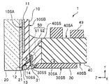
- FIG. 2 is a cross-sectional view taken along the line II-II in FIG. 1 of the imaging apparatus according to the first embodiment.
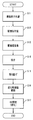
- It is a flowchart for demonstrating the manufacturing method of the imaging device of 1st Embodiment. It is sectional drawing for demonstrating the manufacturing method of the imaging device of 1st Embodiment. It is sectional drawing for demonstrating the manufacturing method of the imaging device of 1st Embodiment. It is sectional drawing for demonstrating the manufacturing method of the imaging device of 1st Embodiment. It is sectional drawing for demonstrating the manufacturing method of the imaging device of 1st Embodiment. It is a perspective view of the image sensor for demonstrating the manufacturing method of the imaging device of 2nd Embodiment. It is a perspective view of the endoscope of a 3rd embodiment.
- FIG. 1 ⁇ First Embodiment>
- FIG. 1 The drawings are schematic, and the relationship between the thickness and width of each member, the ratio of the thickness of each member, the number of electrodes, the array pits, and the like are different from the actual ones. Moreover, the part from which the relationship and ratio of a mutual dimension differ also in between drawings is contained. Furthermore, some configurations, for example, a silicon oxide layer on the surface of the image sensor, are not shown.
- the imaging device 1 includes an imaging element 10, a cover glass 20, a first wiring board 30, a second wiring board 40, and a curable resin 50. .
- a signal cable (not shown) is joined to the second wiring board 40.
- the imaging element 10 made of silicon includes a light receiving surface 10SA on which the light receiving unit 11 is formed, a back surface 10SB facing the light receiving surface 10SA, and an inclined surface 10SS inclined at an acute angle ⁇ with respect to the light receiving surface 10SA. And having. On the light receiving surface 10SA, the first electrodes 12 electrically connected to the light receiving unit 11 are arranged.
- the first electrode 12 is covered with a cover glass 20 through an adhesive layer 21. However, the back surface of the first electrode 12 is exposed to the back surface 10SB side, and is connected to the second electrode 14 of the back surface 10SB via the wiring 13.
- the flexible first wiring board 30 has an upper surface 30SA, a lower surface 30SB facing the upper surface 30SA, and an end surface 30SS orthogonal to the upper surface 30SA.
- a plurality of flying leads 31 protrude from the end face 30SS.
- the non-flexible second wiring board 40 includes a first main surface 40SA, a second main surface 40SB that faces the first main surface 40SA, and a tip surface 40SS that is orthogonal to the first main surface 40SA. .
- the upper surface 30SA of the first wiring board 30 is bonded to the second main surface 40SB of the second wiring board 40.
- the end surface 40SS of the second wiring board 40 is bonded to the back surface 10SB of the imaging element 10 via an adhesive member 52 made of a curable resin. That is, the front end surface 30SS of the first wiring board 30 and the end surface 40SS of the second wiring board 40 are arranged in parallel to the back surface 10SB of the image sensor 10.
- the first wiring board 30 and the second wiring board 40 are viewed in a plan view from the thickness direction (Z direction) of the image sensor 10, the first circuit board 30 and the second circuit board 40 are located within the area inside the image sensor 10, that is, within the projection plane of the image sensor 10. The whole is arranged. Further, a signal cable (not shown) does not protrude outside the outer shape of the image sensor 10. For this reason, the imaging device 1 has a small diameter.
- the front end face 30 SS and the second wiring board 40 of the first wiring board 30 are arranged.
- the end surface 40SS of the image sensor 10 may be inclined rather than parallel to the back surface 10SB of the image sensor 10. That is, it is only necessary that the front end surface 30SS of the first wiring board 30 and the end surface 40SS of the second wiring board 40 are opposed to the back surface 10SB of the imaging element 10.
- the flying lead 31 of the first wiring board 30 is bent at a substantially right angle, and the tip thereof is joined to the second electrode 14 of the image sensor 10.
- the joint between the second electrode 14 of the image sensor 10 and the tip of the flying lead 31 is sealed with a sealing member 51 made of a curable resin.
- the sealing member 51 and the adhesive member 52 are configured by an integral curable resin 50. That is, as will be described later, the adhesion and fixing of the second wiring board 40 to the image sensor 10 and the sealing of the joint between the second electrode 14 and the flying lead 31 are performed simultaneously. In other words, the sealing member 51 and the adhesive member 52 are simultaneously cured.
- the imaging device 1 is easy to manufacture because the sealing member 51 and the adhesive member 52 are constituted by the integral curable resin 50. Furthermore, since the sealing portion is mechanically reinforced by the sealing member 51, the imaging device 1 has no possibility of being damaged even when stress is applied, and has high reliability.
- the image sensor 10 is manufactured by a wafer process in which a large number of image sensors are manufactured by a semiconductor manufacturing technique.
- a plurality of light receiving portions 11 made of a CMOS (Complementary Metal Oxide Semiconductor) image sensor, a CCD (Charge Coupled Device), or the like is formed on a silicon wafer.
- a plurality of first electrodes 12 for supplying an electrical signal to the light receiving unit 11 and transmitting an imaging signal from the light receiving unit 11 are disposed around each light receiving unit 11.
- the glass wafer is bonded to the light receiving surface of the silicon wafer with an adhesive made of a transparent ultraviolet curable resin, and a bonded wafer is manufactured.
- a microlens array may be provided on the light receiving unit 11 and the periphery of the light receiving unit 11 may be bonded with a light-shielding adhesive.
- a through trench whose wall surface is the inclined surface 10SS is formed so that the back surface of the first electrode 12 is exposed on the back surface side of the bonded wafer.
- anisotropic etching can be preferably used.
- a wet etching method using a tetramethylammonium hydroxide (TMAH) aqueous solution, a potassium hydroxide (KOH) aqueous solution or the like is desirable, but reactive ion etching (RIE), chemical dry etching (CDE), etc.
- RIE reactive ion etching
- CDE chemical dry etching
- anisotropic etching is performed on the (111) surface which is slower than the (100) surface.
- the wall surface becomes a (111) plane, and an inclined surface 10SS with an acute angle of 54.74 degrees with the (100) plane which is the light receiving surface 10SA.
- the wiring 13 is disposed from the back surface of the first electrode 12 exposed on the back surface 10SB to the back surface 10SB.
- the second electrode 14 is disposed on the wiring 13 on the back surface 10SB.
- the second electrode 14 is, for example, a solder bump or a gold bump formed by frame plating or paste printing.
- the first electrode 12 and the second electrode 14 may be connected by a through wiring instead of the wiring 13.
- the W-CSP type imaging device 10 in which the light receiving surface 10SA is covered with the cover glass 20 and the second electrode 14 is disposed on the back surface 10SB is manufactured.
- the first wiring board 30 is a flexible wiring board having a plurality of wirings, for example, made of polyimide as an insulating layer. As for the 1st wiring board 30, the flying lead 31 protrudes from end surface 30SS. That is, the first wiring board 30 is bonded to the image sensor 10 by TAB (Tape Automated Bonding) technology.
- the flying lead 31 is also called an inner lead in the lead frame, but is a rod-shaped metal conductor formed by selectively peeling off the insulating layer around the wiring of the wiring board 30.
- the wiring board 30 may be a double-sided wiring board or a multilayer wiring board.
- the second wiring board 40 is an inflexible rigid wiring board. That is, the second wiring board 40 has a thickness (Y-axis dimension) as large as 300 ⁇ m, for example, and a large area of the tip end surface 40SS.
- An electronic component 49 such as a chip capacitor is mounted on the first main surface 40SA of the second wiring board 40.
- the second wiring board 40 may be a component built-in wiring board.
- Step S13> Bonding of Wiring Board The upper surface 30SA of the first wiring board 30 and the second main surface 40SB of the second wiring board 40 are bonded. Simultaneously with the bonding, the electrode on the upper surface of the first wiring board 30 and the electrode on the second main surface of the second wiring board 40 are joined and electrically connected.
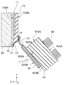
- Step S14 Flying Lead Joining As shown in FIG. 4A, the flying lead 31 of the first wiring board 30 and the second electrode 14 on the back surface 10SB of the image sensor 10 are joined.
- Bonding is solder bonding or ultrasonic bonding.
- Step S15 Flying Lead Bending As shown in FIG. 4B, the flying lead 31 is bent so that the front end surface 40SS of the second wiring board 40 is parallel to the back surface 10SB of the image sensor 10.
- an uncured liquid curable resin 50L is injected between the back surface 10SB of the image sensor 10 and the tip surface 40SS of the second wiring board 40. At this time, not only the bonding portion 52L between the back surface 10SB and the tip surface 40SS but also the bonding portion 51L between the flying lead 31 and the second electrode 14 is covered with the curable resin 50L.
- the curable resin a thermosetting resin or an ultraviolet curable resin can be used, but an ultraviolet curable resin is preferable from the viewpoint of workability.
- an ultraviolet curable resin a silicone resin, an epoxy resin, an acrylic resin, or the like is used.
- an uncured curable resin may be injected into a predetermined location before the flying lead bending step.
- Step S17> Curing Process As shown in FIG. 5, a curing process for irradiating the uncured and liquid curable resin 50L with ultraviolet rays (UV) is performed. By the curing process, the curable resin 50L is solidified, the joint portion 51 is sealed, and the adhesive portion 52 is fixed.
- UV ultraviolet rays
- the curing process for sealing the bonding part 51 and the curing process for fixing the bonding part 52 are performed simultaneously. For this reason, the manufacturing method of the imaging device 1 is easy to manufacture.
- the imaging device 1 is inserted into a frame body of an insertion tip of an endoscope. Since the imaging device 1 manufactured by the manufacturing method of the imaging device of the embodiment is sealed and fixed with a curable resin, for example, stress is applied when inserted into the frame body. There is no risk of breakage, and reliability is high.
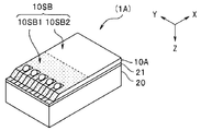
- an imaging device 1A according to a modification of the second embodiment will be described. Since the imaging apparatus 1A is similar to the imaging apparatus 1 and has the same effect, components having the same function are denoted by the same reference numerals and description thereof is omitted.
- the imaging device 1A is the same as the imaging device 1 in appearance and is not easy to distinguish.
- the area where the curable resin 50 is disposed on the back surface 10SB of the imaging element 10 is a preset range, for example, an area up to 250 ⁇ m, which is half of the length direction (X direction). It has become.
- the uncured and liquid curable resin 50L has different wettability depending on the state of the disposed surface.
- “Wettability” is the affinity of a liquid for a solid surface and is expressed as hydrophilic or hydrophobic when the liquid is water. “Wettability” can be quantified by the contact angle ⁇ when a liquid is dropped on the surface. The smaller the contact angle ⁇ , the larger the liquid disposed on the surface. On the other hand, the liquid is difficult to spread on the surface having a large contact angle ⁇ .
- the uncured liquid curable resin 50L exhibits the same properties as water. That is, the curable resin 50L tends to spread on the hydrophilic surface and hardly spread on the hydrophobic surface.
- the sealing portion and the adhesive portion are simultaneously cured, it is necessary to inject a relatively large amount of the curable resin 50L.
- the curable resin 50L spreads widely on the back surface 10SB, not only the resin remaining in the sealing portion is reduced and sealing may be insufficient, but also there is a possibility of adversely affecting the joining of the signal cable.
- the excessively injected curable resin 50L spreads on the side surface of the image pickup device 10, the diameter reduction is hindered.
- the curable resin 50L spreads to the light receiving surface 10SA, the captured image is adversely affected.
- the manufacturing method of the image pickup apparatus 1A includes a step of hydrophilizing the surface of the region where the curable resin 50 of the image pickup element 10 is disposed. Therefore, the contact angle ⁇ 1 of the region 10SB1 in which the curable resin 50 is disposed with the uncured liquid curable resin 50L is smaller than the contact angle ⁇ 2 of the region 10SB2 in which the curable resin 50 is not disposed. .
- the contact angle ⁇ 2 of the region 10SB2 where the curable resin 50 is not disposed is 20 degrees to 30 degrees, but the contact angle ⁇ 1 of the region 10SB1 where the curable resin 50 is disposed is 10 degrees or less. Is preferred.
- Hydrophilic treatment is performed by ultraviolet irradiation, oxygen plasma irradiation, hydrophilic polymer coating, blasting, or the like.
- a Si bond is opened by ultraviolet treatment, and a hydroxyl group (—OH) is formed on the surface by bonding with water in the atmosphere.
- a hydrophilic functional group such as a carboxyl group may be introduced on the surface by CVD or the like.
- a region where the curable resin 50 is not desired to be disposed, in other words, a region where the curable resin 50 is not preferably spread is covered with a resist mask or the like so as not to be irradiated with ultraviolet rays before the hydrophilic treatment.
- the hydrophilization treatment may be performed by a wafer process at the time of manufacturing the image sensor as long as the uncured curable resin 50L is not disposed, or may be performed after the individual image sensor is separated into individual pieces. .
- the image pickup apparatus 1A Even if the curable resin 50L is excessively injected, the image pickup apparatus 1A spreads widely on the back surface 10SB, and there is a possibility that the sealing portion may be insufficiently sealed or may extend to the side surface or the light receiving surface of the image pickup element 10. Absent.
- the endoscope 9 according to the third embodiment will be described. Since the imaging devices 1 and 1A of the endoscope 9 are the same as the imaging device 1 and the like of the embodiment, description thereof is omitted. Hereinafter, the endoscope 9 having the imaging device 1 will be described as an example.
- the endoscope 9 is provided with an image pickup apparatus 1 having an image pickup device having a high number of pixels on the distal end side 9 ⁇ / b> A and an insertion portion 9 ⁇ / b> B provided on the distal end portion hardness 9 ⁇ / b> A. 9C and a universal cord 9D extending from the operation unit 9C.
- the endoscope 9 is minimally invasive because it has the thin imaging device 1 at the distal end rigid portion of the insertion portion. Furthermore, since the joint portion is sealed and fixed with a curable resin, the imaging device 1 is highly reliable without being damaged even when stress is applied when inserted into the distal end hard portion or in use.
- the present invention is not limited to the above-described embodiment or modification, and various changes, modifications, combinations, and the like can be made without departing from the scope of the present invention.
Landscapes
- Health & Medical Sciences (AREA)
- Life Sciences & Earth Sciences (AREA)
- Surgery (AREA)
- Engineering & Computer Science (AREA)
- Physics & Mathematics (AREA)
- Biomedical Technology (AREA)
- Animal Behavior & Ethology (AREA)
- Radiology & Medical Imaging (AREA)
- Optics & Photonics (AREA)
- Nuclear Medicine, Radiotherapy & Molecular Imaging (AREA)
- Biophysics (AREA)
- Heart & Thoracic Surgery (AREA)
- Medical Informatics (AREA)
- Molecular Biology (AREA)
- Pathology (AREA)
- General Health & Medical Sciences (AREA)
- Public Health (AREA)
- Veterinary Medicine (AREA)
- Manufacturing & Machinery (AREA)
- Endoscopes (AREA)
- Studio Devices (AREA)
- Geometry (AREA)
Abstract
撮像装置1は、受光面10SAの第1の電極12と裏面10SBの第2の電極14とを接続している配線13を有する撮像素子10と、フライングリード31が突出している端面30SSが撮像素子10の裏面10SBに対して対向配置されている第1配線板30と、第2の主面40SBに第1配線板30の上面30SAが接着されており先端面40SSが裏面10SBに対して対向配置されている第2配線板40と、を具備し、フライングリード31が折り曲げられ第2の電極14と接合されており、第2の電極14とフライングリード31との接合部を封止している封止部材51と、第2配線板40の先端面40SSと裏面10SBとを接着している接着部材52とが一体の硬化型樹脂50により構成されている。
Description
本発明は、撮像素子と、前記撮像素子の裏面の電極と接合されているフライングリードを有する第1配線板と、第2の主面が第1配線板に接着され先端面が前記撮像素子に接着されている第2配線板と、を具備する撮像装置、前記撮像装置を先端硬性部に有する内視鏡、及び、前記撮像装置の製造方法に関する。
内視鏡の先端硬性部に配設される撮像装置は低侵襲化のために小型化が強く要望されている。また、上記撮像装置は、先端硬性部の枠体への挿入時や使用時に応力が印加されるため破損するおそれがあった。
日本国特開2015-8901号公報には、撮像素子の受光面の電極と第1基板のインナーリード(フライングリード)との接合部を封止樹脂により封止するとともに、第1基板が接着された第2基板の先端面とを撮像素子の裏面とを接着剤で接着し固定した撮像ユニットが開示されている。第1基板は可撓性配線板であり、第2基板は第1基板よりも厚い非可撓性配線板である。
上記撮像ユニットでは、接合部を封止樹脂により封止した後に、第2基板を接着剤により接着するため、工程が繁雑であった。
また、日本国特開2014-75764号公報には、ウエハレベルチップサイズパッケージ(W-CSP)技術により作製される撮像装置が開示されている。W-CSP型の撮像装置の製造方法では、最初に、半導体ウエハの受光面に、複数の受光部と、それぞれの受光部と電気的に接続された複数の外部電極が形成される。半導体ウエハの受光面にガラスウエハが接着され接合ウエハが作製される。そして、接合ウエハの受光面から対向する裏面まで到達する配線が形成され、受光面の外部電極と裏面の電極とは電気的に接続される。接合ウエハを切断することで複数の撮像素子が作製される。そして撮像素子の裏面の電極に配線板の電極が接合される。
上記撮像装置は撮像素子に配線板が接合されただけの状態で枠体の内部に挿入され、その後、枠体の内部に封止樹脂が充填される。
このため、上記撮像装置は枠体の内部に挿入されるときに、応力が印加されると破損するおそれがあった。
本発明は、製造が容易で信頼性が高い撮像装置、前記撮像装置を先端硬性部に有する内視鏡、及び前記撮像装置の製造方法を提供することを目的とする。
本発明の実施形態の撮像装置は、受光面と前記受光面と対向する裏面とを有し、前記受光面の第1の電極と前記裏面の第2の電極とを接続している配線を有する撮像素子と、上面と前記上面と対向する下面と前記上面と直交する端面とを有し、フライングリードが突出している前記端面が前記撮像素子の前記裏面に対して対向配置されている第1配線板と、第1の主面と前記第1の主面と対向する第2の主面と前記第1の主面と直交する先端面とを有し、前記第2の主面に前記第1配線板の前記上面が接着されており、前記先端面が前記撮像素子の前記裏面に対して対向配置されている第2配線板と、を具備し、前記フライングリードが折り曲げられ、その先端部が前記撮像素子の前記第2の電極と接合されており、前記撮像素子の前記第2の電極と前記フライングリードの前記先端部との接合部が封止部材により封止されており、前記第2配線板の前記先端面が、前記撮像素子の前記裏面と接着部材を介して接着されており、前記封止部材と前記接着部材とが一体の硬化型樹脂により構成されている。
別の実施形態の内視鏡は、受光面と前記受光面と対向する裏面とを有し、前記受光面の第1の電極と前記裏面の第2の電極とを接続している配線を有する撮像素子と、上面と前記上面と対向する下面と前記上面と直交する端面とを有し、フライングリードが突出している前記端面が前記撮像素子の前記裏面に対して対向配置されている第1配線板と、第1の主面と前記第1の主面と対向する第2の主面と前記第1の主面と直交する先端面とを有し、前記第2の主面に前記第1配線板の前記上面が接着されており、前記先端面が前記撮像素子の前記裏面に対して対向配置されている第2配線板と、を具備し、前記フライングリードが折り曲げられ、その先端部が前記撮像素子の前記第2の電極と接合されており、前記撮像素子の前記第2の電極と前記フライングリードの前記先端部との接合部が封止部材により封止されており、前記第2配線板の前記先端面が、前記撮像素子の前記裏面と接着部材を介して接着されており、前記封止部材と前記接着部材とが一体の硬化型樹脂により構成されている撮像装置を先端硬性部に有する。
また別の実施形態の撮像装置の製造方法は、受光面と前記受光面と対向する裏面とを有し、前記受光面の第1の電極と前記裏面の第2の電極とを接続している配線を有する撮像素子と、端面からフライングリードが突出している第1配線板と、前記第1配線板が接着されている第2配線板と、を具備する撮像装置の製造方法であって、前記撮像素子の前記第2の電極と、前記フライングリードの先端部を接合する工程と、前記フライングリードを折り曲げながら、前記第1配線板を前記第2配線板に接着する工程と、前記第2の電極と前記先端部との接合部を封止する封止部材、及び、前記第2配線板の先端面と前記撮像素子の前記裏面との間の接着部材、を構成する一体の硬化型樹脂を硬化処理する工程と、を具備する。
本発明によれば、製造が容易で信頼性が高い撮像装置、前記撮像装置を先端硬性部に有する内視鏡、及び前記撮像装置の製造方法を提供できる。
<第1実施形態>
以下、図面を参照して本発明の第1実施形態の撮像装置1を説明する。尚、図面は模式的なものであり、各部材の厚みと幅との関係、それぞれの部材の厚みの比率、電極の数、配列ピットなどは現実のものとは異なる。また、図面の相互間においても互いの寸法の関係や比率が異なる部分が含まれている。さらに、一部の構成、例えば、撮像素子の表面の酸化シリコン層等は図示を省略している。
以下、図面を参照して本発明の第1実施形態の撮像装置1を説明する。尚、図面は模式的なものであり、各部材の厚みと幅との関係、それぞれの部材の厚みの比率、電極の数、配列ピットなどは現実のものとは異なる。また、図面の相互間においても互いの寸法の関係や比率が異なる部分が含まれている。さらに、一部の構成、例えば、撮像素子の表面の酸化シリコン層等は図示を省略している。
図1及び図2に示すように、撮像装置1は、撮像素子10と、カバーガラス20と、第1の配線板30と、第2の配線板40と、硬化型樹脂50と、を具備する。第2の配線板40には信号ケーブル(不図示)が接合されている。
シリコンからなる撮像素子10は、受光部11が形成された受光面10SAと、受光面10SAと対向している裏面10SBと、受光面10SAに対して鋭角の角度θで傾斜している傾斜面10SSと、を有する。受光面10SAには、受光部11と電気的に接続された第1の電極12が列設されている。
第1の電極12は接着層21を介してカバーガラス20に覆われている。しかし第1の電極12は裏面が裏面10SB側に露出しており、配線13を介して、裏面10SBの第2の電極14と接続されている。
可撓性の第1の配線板30は、上面30SAと上面30SAと対向する下面30SBと上面30SAと直交する端面30SSとを有する。端面30SSからは、複数のフライングリード31が突出している。
非可撓性の第2の配線板40は第1の主面40SAと第1の主面40SAと対向する第2の主面40SBと第1の主面40SAと直交する先端面40SSとを有する。第2の配線板40の第2の主面40SBには、第1の配線板30の上面30SAが接着されている。
そして、第2の配線板40の端面40SSは、硬化型樹脂からなる接着部材52を介して、撮像素子10の裏面10SBに接着されている。すなわち、第1の配線板30の先端面30SS及び第2の配線板40の端面40SSは、撮像素子10の裏面10SBに対して平行に配置されている。
このため、第1の配線板30及び第2の配線板40は、撮像素子10の厚み方向(Z方向)から平面視すると、撮像素子10の内側の領域、すなわち撮像素子10の投影面内に、全体が配置されている。さらに図示しない信号ケーブルも撮像素子10の外形よりも外側にはみ出していない。このため、撮像装置1は細径である。
なお、第1の配線板30及び第2の配線板40は撮像素子10の投影面内に、全体が配置されていれば、第1の配線板30の先端面30SS及び第2の配線板40の端面40SSが、撮像素子10の裏面10SBに対して平行ではなく傾斜していてもよい。すなわち、第1の配線板30の先端面30SS及び第2の配線板40の端面40SSは、撮像素子10の裏面10SBに対して対向配置されていればよい。
第1の配線板30のフライングリード31は、略直角に折り曲げられ、その先端部が撮像素子10の第2の電極14と接合されている。撮像素子10の第2の電極14とフライングリード31の先端部との接合部は硬化型樹脂からなる封止部材51により封止されている。
撮像装置1では、封止部材51と接着部材52とが一体の硬化型樹脂50により構成されている。すなわち後述するように、撮像素子10への第2の配線板40の接着固定と、第2の電極14とフライングリード31との接合部の封止と、が同時に行われる。言い替えれば、封止部材51と接着部材52とが同時に硬化処理されている。
撮像装置1は、封止部材51と接着部材52とが一体の硬化型樹脂50により構成されているため、製造が容易である。さらに、撮像装置1は、封止部材51により封止部が機械的に補強されているため、応力が印加されても破損するおそれがなく、信頼性が高い。
なお、封止部材51と接着部材52とが同時に硬化処理されていることを構造上又は特性上、明確に特定することはできない。さらに、その構造を測定に基づき解析することにより特定することも、現在の解析技術からして、不可能である。
<撮像装置の製造方法>
図3のフローチャートに沿って、撮像装置1の製造方法について説明する。
図3のフローチャートに沿って、撮像装置1の製造方法について説明する。
<ステップS11>撮像素子作製
撮像素子10は、半導体製造技術により、多数の撮像素子がウエハプロセスで製造される。シリコンウエハにCMOS(Complementary Metal Oxide Semiconductor)イメージセンサ、又は、CCD(Charge Coupled Device)等からなる複数の受光部11が形成される。受光部11に電気信号を供給したり、受光部11からの撮像信号が送信したりする複数の第1の電極12が、それぞれの受光部11の周囲に配設される。
撮像素子10は、半導体製造技術により、多数の撮像素子がウエハプロセスで製造される。シリコンウエハにCMOS(Complementary Metal Oxide Semiconductor)イメージセンサ、又は、CCD(Charge Coupled Device)等からなる複数の受光部11が形成される。受光部11に電気信号を供給したり、受光部11からの撮像信号が送信したりする複数の第1の電極12が、それぞれの受光部11の周囲に配設される。
そして、透明な紫外線硬化型樹脂からなる接着剤によりガラスウエハが、シリコンウエハの受光面に接着され、接合ウエハが作製される。なお、受光部11の上にマイクロレンズアレイを配設し、受光部11の周囲を、遮光性の接着剤により接着してもよい。
接合ウエハの裏面側に第1の電極12の裏面が露出するように、壁面が傾斜面10SSである貫通トレンチが形成される。傾斜面10SSを有する貫通トレンチの形成には、異方性エッチングを好ましく用いることができる。異方性エッチングとしては、水酸化テトラメチルアンモニウム(TMAH)水溶液、水酸化カリウム(KOH)水溶液などを用いるウエットエッチング法が望ましいが、反応性イオンエッチング(RIE)、ケミカルドライエッチング(CDE)などのドライエッチング法も用いることができる。
たとえば、撮像素子10として受光面10SAが(100)面のシリコン基板を用いた場合には、(111)面のエッチング速度が(100)面に比べて遅い異方性エッチングとなるため、貫通トレンチの壁面は(111)面となり、受光面10SAである(100)面との角度θが鋭角の54.74度の傾斜面10SSとなる。
次に裏面10SBに露出した第1の電極12の裏面から裏面10SBまで配線13が配設される。そして、裏面10SBの配線13に第2の電極14が配設される。第2の電極14は例えば、フレームめっき法もしくはペースト印刷法により形成された半田バンプ又は金バンプ等である。
なお、第1の電極12と第2の電極14とが、配線13に替えて、貫通配線で接続されていてもよい。
そして、接合ウエハを切断することにより、受光面10SAがカバーガラス20で覆われ、裏面10SBに第2の電極14が配設された、W-CSP型の撮像素子10が作製される。
<ステップS12>配線板作製
第1の配線板30は、例えばポリイミドを絶縁層とする、複数の配線を有するフレキシブル配線板である。第1の配線板30は、端面30SSからフライングリード31が突出している。すなわち、第1の配線板30は、TAB(Tape Automated Bonding)技術により撮像素子10と接合される。
第1の配線板30は、例えばポリイミドを絶縁層とする、複数の配線を有するフレキシブル配線板である。第1の配線板30は、端面30SSからフライングリード31が突出している。すなわち、第1の配線板30は、TAB(Tape Automated Bonding)技術により撮像素子10と接合される。
フライングリード31は、リードフレームではインナーリードとも呼ばれているが、配線板30の配線の周囲の絶縁層等を選択的に剥離することにより形成される棒状の金属導体である。配線板30は両面配線板又は多層配線板であってもよい。
一方、第2の配線板40は、非可撓性のリジット配線板である。すなわち、第2の配線板40は厚さ(Y軸寸法)が、例えば300μmと厚く、先端面40SSの面積が広い。第2の配線板40の第1の主面40SAにはチップコンデンサ等の電子部品49が実装されている。なお、第2の配線板40は部品内蔵配線板でもよい。
<ステップS13>配線板接着
第1の配線板30の上面30SAと、第2の配線板40の第2の主面40SBとが接着される。接着と同時に、第1の配線板30の上面の電極と、第2の配線板40の第2の主面の電極とが接合され、電気的に接続される。
第1の配線板30の上面30SAと、第2の配線板40の第2の主面40SBとが接着される。接着と同時に、第1の配線板30の上面の電極と、第2の配線板40の第2の主面の電極とが接合され、電気的に接続される。
<ステップS14>フライングリード接合
図4Aに示すように、第1の配線板30のフライングリード31と撮像素子10の裏面10SBの第2の電極14とが接合される。
図4Aに示すように、第1の配線板30のフライングリード31と撮像素子10の裏面10SBの第2の電極14とが接合される。
接合は、半田接合又は超音波接合である。
<ステップS15>フライングリード折り曲げ
図4Bに示すように、第2の配線板40の先端面40SSが、撮像素子10の裏面10SBと平行になるように、フライングリード31が折り曲げられる。
図4Bに示すように、第2の配線板40の先端面40SSが、撮像素子10の裏面10SBと平行になるように、フライングリード31が折り曲げられる。
<ステップS16>硬化型樹脂配設
図5に示すように、撮像素子10の裏面10SBと第2配線板40の先端面40SSとの間に未硬化で液体の硬化型樹脂50Lが注入される。このとき、裏面10SBと先端面40SSとの接着部52Lだけでなく、フライングリード31と第2の電極14との接合部51Lも硬化型樹脂50Lで覆われる。
図5に示すように、撮像素子10の裏面10SBと第2配線板40の先端面40SSとの間に未硬化で液体の硬化型樹脂50Lが注入される。このとき、裏面10SBと先端面40SSとの接着部52Lだけでなく、フライングリード31と第2の電極14との接合部51Lも硬化型樹脂50Lで覆われる。
硬化型樹脂としては、熱硬化型樹脂または紫外線硬化型樹脂を用いることができるが、作業性の観点から紫外線硬化型樹脂が好ましい。紫外線硬化樹脂としては、シリコーン系樹脂、エポキシ系樹脂、またはアクリル系樹脂等を用いる。
なお、フライングリード折り曲げ工程の前に、未硬化の硬化型樹脂が所定箇所に注入されてもよい。
<ステップS17>硬化処理
図5に示すように、未硬化で液体の硬化型樹脂50Lに紫外線(UV)を照射する硬化処理が行われる。硬化処理により、硬化型樹脂50Lは固体化し、接合部51は封止され接着部52は固定される。
図5に示すように、未硬化で液体の硬化型樹脂50Lに紫外線(UV)を照射する硬化処理が行われる。硬化処理により、硬化型樹脂50Lは固体化し、接合部51は封止され接着部52は固定される。
撮像装置1の製造方法によれば、接合部51の封止のための硬化処理と、接着部52の固定のための硬化処理と、が同時に行われる。このため、撮像装置1の製造方法は製造が容易である。
なお、撮像装置1は後述するように、例えば内視鏡の挿入先端部の枠体の内部に挿入される。実施形態の撮像装置の製造方法で製造された撮像装置1は、接合部が硬化型樹脂で封止され固定されているため、例えば、枠体の内部に挿入されるときに、応力が印加されても破損するおそれがなく、信頼性が高い。
<第2実施形態>
次に第2実施形態の変形例の撮像装置1Aについて説明する。撮像装置1Aは、撮像装置1と類似し同じ効果を有しているため、同じ機能の構成要素には同じ符号を付し説明は省略する。
次に第2実施形態の変形例の撮像装置1Aについて説明する。撮像装置1Aは、撮像装置1と類似し同じ効果を有しているため、同じ機能の構成要素には同じ符号を付し説明は省略する。
撮像装置1Aは、外観上は撮像装置1と同じで区別することは容易ではない。しかし、撮像装置1Aでは、撮像素子10の裏面10SBにおける硬化型樹脂50の配設されている領域が、予め設定された範囲、例えば、長さ方向(X方向)の半分の250μmまでの領域となっている。
未硬化で液状の硬化型樹脂50Lは、配設された表面の状態により、濡れ性が異なる。「濡れ性」は固体表面に対する液体の親和性であり、液体が水の場合には、親水性又は疎水性として表現される。「濡れ性」は、表面に液体を滴下したときの接触角φで数値化できる。接触角φが小さいほど、表面に配設された液体は大きく広がる。反対に接触角φが大きい表面では液体は広がりにくい。
撮像素子10Aでは、未硬化液状の硬化型樹脂50Lは、水と同様の性質を示す。すなわち、硬化型樹脂50Lは、親水性表面には広がりやすく、疎水性表面には広がりにくい。
撮像装置1では、封止部と接着部とを同時に硬化処理するため、比較的、大量の硬化型樹脂50Lを注入する必要がある。しかし、硬化型樹脂50Lが裏面10SBに大きく広がると封止部に残る樹脂が少なくなり封止が不十分になるおそれがあるだけでなく、信号ケーブルの接合に悪影響を及ぼすおそれがある。また過剰に注入された硬化型樹脂50Lが撮像素子10の側面に広がると細径化の妨げとなる。また、硬化型樹脂50Lが受光面10SAまで広がると撮像画像に悪影響を及ぼす。
このため、撮像装置1Aの製造方法では撮像素子10の硬化型樹脂50が配設される領域の表面を、親水化処理する工程を具備する。このため、硬化型樹脂50が配設される領域10SB1の、未硬化液状の硬化型樹脂50Lとの接触角φ1が、硬化型樹脂50が配設されていない領域10SB2の接触角φ2よりも小さい。
例えば、硬化型樹脂50が配設されていない領域10SB2の接触角φ2は20度~30度であるが、硬化型樹脂50が配設される領域10SB1の接触角φ1は10度以下とすることが好ましい。
親水化処理は、紫外線照射、酸素プラズマ照射、親水性ポリマーのコーティング、又は、ブラスト加工等により行う。例えば、裏面10SBは酸化シリコン膜で覆われているが、紫外線処理によりSi結合が開環し、大気中の水と結合とすることで表面に水酸基(-OH)が形成される。より強い親水性を付与するために、CVD等により、カルボキシル基等の親水性官能基を表面に導入してもよい。
硬化型樹脂50を配設したくない領域、言い替えれば、硬化型樹脂50が広がることが好ましくない領域は、親水化処理の前に、紫外線が照射されないようにレジストマスク等で覆われる。なお、親水化処理は、未硬化の硬化型樹脂50Lを配設する前であれば、撮像素子作製時のウエハプロセスで行ってもよいし、個々の撮像素子に個片化後におこなってもよい。
撮像装置1Aは、硬化型樹脂50Lが過剰に注入されても裏面10SBに大きく広がり、封止部の封止が不十分になったり、撮像素子10の側面や受光面にまで広がったりするおそれがない。
<第3実施形態>
次に、第3実施形態の内視鏡9について説明する。内視鏡9の撮像装置1、1Aは、実施形態の撮像装置1等と同じであるため説明は省略する。以下、撮像装置1を有する内視鏡9を例に説明する。
次に、第3実施形態の内視鏡9について説明する。内視鏡9の撮像装置1、1Aは、実施形態の撮像装置1等と同じであるため説明は省略する。以下、撮像装置1を有する内視鏡9を例に説明する。
図7に示すように、内視鏡9は、高画素数の撮像素子を有する撮像装置1が先端部硬性9Aに配設された挿入部9Bと、挿入部9Bの基端側に配設された操作部9Cと、操作部9Cから延出するユニバーサルコード9Dと、を具備する。
内視鏡9は細径の撮像装置1を挿入部の先端硬性部に有するため低侵襲である。さらに、撮像装置1は接合部が硬化型樹脂で封止され固定されているため、先端硬性部に挿入される時や使用時に、応力が印加されても破損するおそれがなく、信頼性が高い
本発明は上述した実施形態、又は変形例等に限定されるものではなく、本発明の要旨を変えない範囲において、種々の変更、改変、組み合わせ等ができる。
本発明は上述した実施形態、又は変形例等に限定されるものではなく、本発明の要旨を変えない範囲において、種々の変更、改変、組み合わせ等ができる。
1、1A…撮像装置
9…内視鏡
11…受光部
12…第1の電極
13…配線
14…第2の電極
20…カバーガラス
21…接着層
30…第1の配線板
31…フライングリード
40…第2の配線板
49…電子部品
50…硬化型樹脂
50L…(未硬化の)硬化型樹脂
51…封止部材
52…接着部材
9…内視鏡
11…受光部
12…第1の電極
13…配線
14…第2の電極
20…カバーガラス
21…接着層
30…第1の配線板
31…フライングリード
40…第2の配線板
49…電子部品
50…硬化型樹脂
50L…(未硬化の)硬化型樹脂
51…封止部材
52…接着部材
Claims (6)
- 受光面と前記受光面と対向する裏面とを有し、前記受光面の第1の電極と前記裏面の第2の電極とを接続している配線を有する撮像素子と、
上面と前記上面と対向する下面と前記上面と直交する端面とを有し、フライングリードが突出している前記端面が前記撮像素子の前記裏面に対向配置されている第1配線板と、
第1の主面と前記第1の主面と対向する第2の主面と前記第1の主面と直交する先端面とを有し、前記第2の主面に前記第1配線板の前記上面が接着されており、前記先端面が前記撮像素子の前記裏面に対向配置されている第2配線板と、を具備し、
前記フライングリードが折り曲げられ、その先端部が前記撮像素子の前記第2の電極と接合されており、
前記撮像素子の前記第2の電極と前記フライングリードの前記先端部との接合部が封止部材により封止されており、
前記第2配線板の前記先端面が、前記撮像素子の前記裏面と接着部材を介して接着されており、
前記封止部材と前記接着部材とが一体の硬化型樹脂により構成されていることを特徴とする撮像装置。 - 前記撮像素子の前記硬化型樹脂が配設されている領域の未硬化液状の前記硬化型樹脂との接触角が、前記硬化型樹脂が配設されていない領域の接触角よりも小さいことを特徴とする請求項1に記載の撮像装置。
- 前記封止部材を構成している前記硬化型樹脂と、前記接着部を構成している前記硬化型樹脂と、が同時に硬化処理されていることを特徴とする請求項1又は請求項2に記載の撮像装置。
- 請求項1から請求項3のいずれか1項に記載の撮像装置を、挿入部の先端硬性部に有することを特徴とする内視鏡。
- 受光面と前記受光面と対向する裏面とを有し、前記受光面の第1の電極と前記裏面の第2の電極とを接続している配線を有する撮像素子と、
端面からフライングリードが突出している第1配線板と、
前記第1配線板が接着されている第2配線板と、を具備する撮像装置の製造方法であって、
前記撮像素子の前記第2の電極と、前記フライングリードの先端部を接合する工程と、
前記フライングリードを折り曲げながら、前記第1配線板を前記第2配線板に接着する工程と、
前記第2の電極と前記先端部との接合部を封止する封止部材、及び、前記第2配線板の先端面と前記撮像素子の前記裏面との間の接着部材、を構成する一体の硬化型樹脂を硬化処理する工程と、を具備することを特徴とする撮像装置の製造方法。 - 前記撮像素子の前記硬化型樹脂が配設される領域の表面を、親水化処理する工程を具備することを特徴とする請求項5に記載の撮像装置の製造方法。
Priority Applications (5)
| Application Number | Priority Date | Filing Date | Title |
|---|---|---|---|
| PCT/JP2016/058144 WO2017158722A1 (ja) | 2016-03-15 | 2016-03-15 | 撮像装置、内視鏡、及び、撮像装置の製造方法 |
| CN201680082552.9A CN108697313A (zh) | 2016-03-15 | 2016-03-15 | 摄像装置、内窥镜和摄像装置的制造方法 |
| DE112016006595.7T DE112016006595T5 (de) | 2016-03-15 | 2016-03-15 | Bildaufnahmevorrichtung, Endoskop und Verfahren zum Herstellen der Bildaufnahmevorrichtung |
| JP2018505107A JP6655710B2 (ja) | 2016-03-15 | 2016-03-15 | 撮像装置、内視鏡、及び、撮像装置の製造方法 |
| US16/118,865 US11134829B2 (en) | 2016-03-15 | 2018-08-31 | Image pickup apparatus, endoscope, and method for manufacturing image pickup apparatus |
Applications Claiming Priority (1)
| Application Number | Priority Date | Filing Date | Title |
|---|---|---|---|
| PCT/JP2016/058144 WO2017158722A1 (ja) | 2016-03-15 | 2016-03-15 | 撮像装置、内視鏡、及び、撮像装置の製造方法 |
Related Child Applications (1)
| Application Number | Title | Priority Date | Filing Date |
|---|---|---|---|
| US16/118,865 Continuation US11134829B2 (en) | 2016-03-15 | 2018-08-31 | Image pickup apparatus, endoscope, and method for manufacturing image pickup apparatus |
Publications (1)
| Publication Number | Publication Date |
|---|---|
| WO2017158722A1 true WO2017158722A1 (ja) | 2017-09-21 |
Family
ID=59850170
Family Applications (1)
| Application Number | Title | Priority Date | Filing Date |
|---|---|---|---|
| PCT/JP2016/058144 Ceased WO2017158722A1 (ja) | 2016-03-15 | 2016-03-15 | 撮像装置、内視鏡、及び、撮像装置の製造方法 |
Country Status (5)
| Country | Link |
|---|---|
| US (1) | US11134829B2 (ja) |
| JP (1) | JP6655710B2 (ja) |
| CN (1) | CN108697313A (ja) |
| DE (1) | DE112016006595T5 (ja) |
| WO (1) | WO2017158722A1 (ja) |
Families Citing this family (2)
| Publication number | Priority date | Publication date | Assignee | Title |
|---|---|---|---|---|
| CN107431782A (zh) * | 2015-03-30 | 2017-12-01 | 奥林巴斯株式会社 | 摄像装置和内窥镜 |
| WO2022254659A1 (ja) * | 2021-06-03 | 2022-12-08 | オリンパスメディカルシステムズ株式会社 | 撮像ユニット、および、内視鏡 |
Citations (6)
| Publication number | Priority date | Publication date | Assignee | Title |
|---|---|---|---|---|
| JP2011249870A (ja) * | 2010-05-21 | 2011-12-08 | Olympus Corp | 撮像装置 |
| JP2013219468A (ja) * | 2012-04-05 | 2013-10-24 | Olympus Corp | 撮像モジュール |
| JP2014075764A (ja) * | 2012-10-05 | 2014-04-24 | Olympus Corp | 撮像装置、該撮像装置を具備する内視鏡 |
| JP2014210041A (ja) * | 2013-04-18 | 2014-11-13 | オリンパス株式会社 | 撮像装置および電子内視鏡 |
| JP2015008901A (ja) * | 2013-06-28 | 2015-01-19 | オリンパス株式会社 | 撮像ユニットおよび内視鏡装置 |
| JP5750642B1 (ja) * | 2013-10-04 | 2015-07-22 | オリンパス株式会社 | 内視鏡用撮像ユニット |
Family Cites Families (7)
| Publication number | Priority date | Publication date | Assignee | Title |
|---|---|---|---|---|
| WO2010119762A1 (ja) * | 2009-04-15 | 2010-10-21 | オリンパスメディカルシステムズ株式会社 | 半導体装置、半導体装置の製造方法 |
| JP5452273B2 (ja) * | 2010-02-15 | 2014-03-26 | オリンパス株式会社 | 半導体装置 |
| JP5314734B2 (ja) * | 2011-07-06 | 2013-10-16 | 富士フイルム株式会社 | 内視鏡 |
| JP5715024B2 (ja) * | 2011-10-27 | 2015-05-07 | オリンパスメディカルシステムズ株式会社 | 撮像ユニット、内視鏡及び撮像ユニットの製造方法 |
| US8916980B2 (en) * | 2012-02-16 | 2014-12-23 | Omnivision Technologies, Inc. | Pad and circuit layout for semiconductor devices |
| WO2014171482A1 (ja) | 2013-04-18 | 2014-10-23 | オリンパス株式会社 | 撮像装置および電子内視鏡 |
| CN107534713A (zh) * | 2015-04-17 | 2018-01-02 | 奥林巴斯株式会社 | 摄像装置 |
-
2016
- 2016-03-15 CN CN201680082552.9A patent/CN108697313A/zh active Pending
- 2016-03-15 JP JP2018505107A patent/JP6655710B2/ja active Active
- 2016-03-15 WO PCT/JP2016/058144 patent/WO2017158722A1/ja not_active Ceased
- 2016-03-15 DE DE112016006595.7T patent/DE112016006595T5/de not_active Withdrawn
-
2018
- 2018-08-31 US US16/118,865 patent/US11134829B2/en active Active
Patent Citations (6)
| Publication number | Priority date | Publication date | Assignee | Title |
|---|---|---|---|---|
| JP2011249870A (ja) * | 2010-05-21 | 2011-12-08 | Olympus Corp | 撮像装置 |
| JP2013219468A (ja) * | 2012-04-05 | 2013-10-24 | Olympus Corp | 撮像モジュール |
| JP2014075764A (ja) * | 2012-10-05 | 2014-04-24 | Olympus Corp | 撮像装置、該撮像装置を具備する内視鏡 |
| JP2014210041A (ja) * | 2013-04-18 | 2014-11-13 | オリンパス株式会社 | 撮像装置および電子内視鏡 |
| JP2015008901A (ja) * | 2013-06-28 | 2015-01-19 | オリンパス株式会社 | 撮像ユニットおよび内視鏡装置 |
| JP5750642B1 (ja) * | 2013-10-04 | 2015-07-22 | オリンパス株式会社 | 内視鏡用撮像ユニット |
Also Published As
| Publication number | Publication date |
|---|---|
| US11134829B2 (en) | 2021-10-05 |
| DE112016006595T5 (de) | 2018-12-13 |
| CN108697313A (zh) | 2018-10-23 |
| JP6655710B2 (ja) | 2020-02-26 |
| US20180368661A1 (en) | 2018-12-27 |
| JPWO2017158722A1 (ja) | 2019-01-17 |
Similar Documents
| Publication | Publication Date | Title |
|---|---|---|
| CN101582435B (zh) | 一种影像感测晶片封装结构及其应用的相机模组 | |
| US9455358B2 (en) | Image pickup module and image pickup unit | |
| US7091599B2 (en) | Solid-state imaging device | |
| US10334143B2 (en) | Image pickup apparatus having wiring board with alternately arranged flying leads | |
| US20080251872A1 (en) | Image sensor package, method of manufacturing the same, and image sensor module including the image sensor package | |
| CN109788892B (zh) | 电子电路单元、摄像单元和内窥镜 | |
| JP5730678B2 (ja) | 撮像装置及びこれを用いた電子機器 | |
| JP2008092417A (ja) | 半導体撮像素子およびその製造方法並びに半導体撮像装置および半導体撮像モジュール | |
| WO2017037828A1 (ja) | 内視鏡、電子ユニットおよび電子ユニットの製造方法 | |
| JP6655710B2 (ja) | 撮像装置、内視鏡、及び、撮像装置の製造方法 | |
| US10217782B2 (en) | Image pickup module and manufacturing method of image pickup module | |
| US10249676B2 (en) | Image pickup apparatus | |
| JPWO2016157376A1 (ja) | 撮像装置および内視鏡 | |
| JPWO2016117123A1 (ja) | 撮像装置、および内視鏡 | |
| WO2018216092A1 (ja) | 撮像モジュールおよび内視鏡 | |
| WO2019077980A1 (ja) | 固体撮像装置 | |
| JP3507472B2 (ja) | 半導体装置、それを用いた固体撮像装置及び撮像システム | |
| JP7270225B2 (ja) | 固体撮像装置 | |
| TW200950021A (en) | Image sensor chip package and camera module using same | |
| WO2016207979A1 (ja) | 半導体装置、および半導体装置の製造方法 |
Legal Events
| Date | Code | Title | Description |
|---|---|---|---|
| ENP | Entry into the national phase |
Ref document number: 2018505107 Country of ref document: JP Kind code of ref document: A |
|
| 121 | Ep: the epo has been informed by wipo that ep was designated in this application |
Ref document number: 16894345 Country of ref document: EP Kind code of ref document: A1 |
|
| 122 | Ep: pct application non-entry in european phase |
Ref document number: 16894345 Country of ref document: EP Kind code of ref document: A1 |