WO2017154751A1 - 試料収容ディスクおよびそれを用いた蛍光検出装置 - Google Patents
試料収容ディスクおよびそれを用いた蛍光検出装置 Download PDFInfo
- Publication number
- WO2017154751A1 WO2017154751A1 PCT/JP2017/008403 JP2017008403W WO2017154751A1 WO 2017154751 A1 WO2017154751 A1 WO 2017154751A1 JP 2017008403 W JP2017008403 W JP 2017008403W WO 2017154751 A1 WO2017154751 A1 WO 2017154751A1
- Authority
- WO
- WIPO (PCT)
- Prior art keywords
- signal
- sample storage
- track
- disk
- sample
- Prior art date
Links
Images


Classifications
-
- G—PHYSICS
- G01—MEASURING; TESTING
- G01N—INVESTIGATING OR ANALYSING MATERIALS BY DETERMINING THEIR CHEMICAL OR PHYSICAL PROPERTIES
- G01N21/00—Investigating or analysing materials by the use of optical means, i.e. using sub-millimetre waves, infrared, visible or ultraviolet light
- G01N21/01—Arrangements or apparatus for facilitating the optical investigation
- G01N21/03—Cuvette constructions
-
- G—PHYSICS
- G01—MEASURING; TESTING
- G01N—INVESTIGATING OR ANALYSING MATERIALS BY DETERMINING THEIR CHEMICAL OR PHYSICAL PROPERTIES
- G01N21/00—Investigating or analysing materials by the use of optical means, i.e. using sub-millimetre waves, infrared, visible or ultraviolet light
- G01N21/62—Systems in which the material investigated is excited whereby it emits light or causes a change in wavelength of the incident light
- G01N21/63—Systems in which the material investigated is excited whereby it emits light or causes a change in wavelength of the incident light optically excited
- G01N21/64—Fluorescence; Phosphorescence
-
- G—PHYSICS
- G01—MEASURING; TESTING
- G01N—INVESTIGATING OR ANALYSING MATERIALS BY DETERMINING THEIR CHEMICAL OR PHYSICAL PROPERTIES
- G01N35/00—Automatic analysis not limited to methods or materials provided for in any single one of groups G01N1/00 - G01N33/00; Handling materials therefor
-
- G—PHYSICS
- G01—MEASURING; TESTING
- G01N—INVESTIGATING OR ANALYSING MATERIALS BY DETERMINING THEIR CHEMICAL OR PHYSICAL PROPERTIES
- G01N37/00—Details not covered by any other group of this subclass
Definitions
- the present invention relates to a sample storage disk for storing a sample prepared by fluorescently staining a subject such as a cell and a fluorescence detection apparatus using the same.
- Patent Document 1 discloses a technique for quickly and easily detecting such cells.
- a fluorescently labeled antigen to be detected is fixed to a track on a disc using the principle of a sandwich method using an antigen-antibody reaction. Thereafter, the track is scanned with laser light serving as excitation light to generate fluorescence from the antigen to be detected, and the antigen to be detected is detected and counted.
- address information in a radial direction and a track direction can be obtained from a disk by recording an address signal in advance in a track portion that is not connected to a flow path into which a sample flows. Describes that the position where the fluorescence is detected can be specified based on the address information.
- Detecting cells infected with pathogenic bacteria or cells having a predetermined form from a large number of cells is particularly important in the medical field such as clinical sites.
- an apparatus for performing such cell detection quickly and easily for example, an apparatus described in Patent Document 2 is known.
- a laser beam is irradiated to a sample containing target cells that are fluorescently labeled. Then, the fluorescence excited from the target cell by the laser light is detected by the photodetector. In this case, since the excited fluorescence is weak, the signal from the photodetector is easily affected by stray light.
- confocality is generated in the fluorescence, and stray light is removed by arranging a pinhole at the confocal position.
- the sample storage disk includes a substrate, a track formed on the upper surface of the substrate so as to turn around the center of the disk, and a sample storage unit disposed on the upper side of the track to store the sample.
- the track is configured to be scanned in the scanning direction. Address signals indicating the positions of the track portions are respectively recorded on the upstream side and the downstream side of the sample storage portion in the scanning direction of the track portion straddling the sample storage portion of the track.
- This sample storage disk can acquire a fluorescent image smoothly.
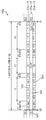
- FIG. 1A is a plan view schematically showing a configuration of a sample storage disk according to the first embodiment.
- FIG. 1B is a view of the sample storage disk shown in FIG. 1A along line 1B-1B.
- FIG. 2 is a diagram schematically showing the structure of grooves, lands, and pits of the sample storage disk according to the first embodiment.
- FIG. 3A is a plan view schematically showing area division in the circumferential direction of the sample storage disk according to the first embodiment.
- FIG. 3B is a plan view schematically showing the zoning in the radial direction of the sample storage disk according to the first embodiment.
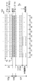
- FIG. 4 is a diagram in which the grooves and lands of each zone of the sample storage disk according to the first embodiment are linearly developed.
- FIG. 5A is a diagram illustrating a format of each field set in a track portion (groove) of one area of the sample storage disk according to the first embodiment.
- FIG. 5B is a diagram schematically illustrating an angle range of each field of the sample storage disk according to the first embodiment.
- FIG. 6A is a diagram illustrating a signal format of each field of the sample storage disk according to the first embodiment.
- FIG. 6B is a schematic enlarged view of the sample storage disk according to the first embodiment.
- FIG. 7 is a configuration diagram of a fluorescence detection pickup for reading fluorescence from the sample storage disk according to the first embodiment.
- FIG. 8 is a diagram illustrating a configuration of a signal calculation circuit of the fluorescence detection pickup according to the first embodiment.
- FIG. 9 is a configuration diagram of the fluorescence detection apparatus according to the first embodiment.
- FIG. 10A is a flowchart illustrating an address signal acquisition process of the fluorescence detection device according to the first embodiment.
- FIG. 10B is a flowchart illustrating the fluorescence signal extraction processing of the fluorescence detection apparatus according to the first embodiment.
- FIG. 11A is a flowchart illustrating a fluorescence signal cut-out process of the fluorescence detection device according to the first embodiment.
- FIG. 11B is a flowchart illustrating a cut-out signal invalidation process of the fluorescence detection device according to the first embodiment.
- FIG. 12 is a diagram for explaining a fluorescence signal cut-out process of the fluorescence detection device according to the first embodiment.
- FIG. 13 is a diagram in which grooves and lands in each zone of the sample storage disk according to the second embodiment are linearly developed.
- FIG. 14A is a diagram illustrating a format of each field set in a track portion of one area of the sample storage disk according to the second embodiment.
- FIG. 14B is a diagram illustrating a configuration for inverting the polarity of the tracking error signal of the fluorescence detection device according to the second embodiment.
- FIG. 14C is a diagram schematically illustrating beam scanning and polarity inversion timing of the tracking error signal in the fluorescence detection device according to the second exemplary embodiment.
- FIG. 14D is a diagram schematically illustrating the structure of grooves, lands, and pits of another sample storage disk according to the second embodiment.
- FIG. 15A is a diagram illustrating a part of the signal format of the sample storage disk according to the third embodiment.
- FIG. 15B is a diagram illustrating a part of the signal format of the sample storage disk according to the third embodiment.
- FIG. 15C is a diagram schematically illustrating the configuration of the synchronization adjustment pit SB1 of the sample storage disk according to the third embodiment.
- FIG. 16 is a diagram illustrating a configuration of the fluorescence detection apparatus according to the third embodiment.
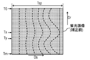
- FIG. 17A is a diagram schematically illustrating the detection position of the synchronization adjustment pit on the signal light image of the fluorescence detection device according to the third exemplary embodiment.
- FIG. 17B is a diagram schematically illustrating a fluorescence image correction process of the fluorescence detection device according to the third embodiment.
- FIG. 17C is a diagram schematically illustrating a fluorescence image correction process of the fluorescence detection device according to the third embodiment.
- FIG. 18 is a diagram illustrating a part of a signal format of another sample storage disk according to the third embodiment.
- FIG. 19 is a diagram illustrating a format of each field set in a track portion (groove) of one area according to the fourth embodiment.
- FIG. 20 is a diagram illustrating a signal format of each field according to the fourth embodiment.
- FIG. 21 is a configuration diagram of a signal calculation circuit and an output processing circuit of the fluorescence detection apparatus according to the fourth embodiment.
- FIG. 22 is a configuration diagram of the fluorescence detection apparatus according to the fourth embodiment.
- FIG. 23A is a configuration diagram of an output processing circuit of a fluorescence detection device of a comparative example.
- FIG. 23B is a diagram schematically illustrating a reproduction RF signal input to the AD conversion circuit of the output processing circuit of the comparative example.
- FIG. 24A is a configuration diagram of an output processing circuit of the fluorescence detection apparatus according to the fourth embodiment.
- FIG. 24B is a diagram schematically illustrating a reproduction RF signal input to the AD conversion circuit of the output processing circuit when the modulation structure is not formed in the groove of the fluorescence detection device according to the fourth exemplary embodiment.
- FIG. 24C is a diagram schematically illustrating a reproduction RF signal input to the AD conversion circuit of the output processing circuit when the modulation structure is formed in the groove of the fluorescence detection device according to the fourth exemplary embodiment.
- FIG. 25A is a configuration diagram of another output processing circuit according to the fourth embodiment.
- FIG. 25B is a configuration diagram of still another output processing circuit according to the fourth embodiment.
- FIG. 25C is a diagram showing a format of a track area of another sample storage disk according to the fourth embodiment.
- FIG. 26A is a flowchart illustrating a process of stopping the output of various signals from the output processing circuit of the fluorescent device according to the fourth embodiment.
- FIG. 26B is a diagram illustrating a configuration of a table referred to in setting a mask period of the fluorescence detection apparatus according to the fourth embodiment.
- FIG. 27 is a diagram showing the format of each field set in the track portion of one area of the sample storage disk according to the fifth embodiment.
- FIG. 28A is a diagram in which grooves and lands of other sample storage disks according to Embodiments 4 and 5 are linearly developed.
- FIG. 28B is a diagram in which grooves and lands of still another sample storage disk according to Embodiments 4 and 5 are linearly developed.
- FIG. 29 is a configuration diagram of the fluorescence detection pickup according to the sixth embodiment.
- FIG. 30A is a configuration diagram of a light shielding body of the fluorescence detection pickup according to the sixth embodiment.
- FIG. 30B is a configuration diagram of another light shielding body of the fluorescence detection pickup according to the sixth embodiment.
- FIG. 30C is a cross-sectional view of the light-shielding unit of the fluorescence detection pickup according to the sixth embodiment.
- FIG. 31 is a cross-sectional view of the light shielding unit according to the sixth embodiment.
- FIG. 32A is a cross-sectional view of the light shielding unit according to Embodiment 6.
- FIG. 32B is a cross-sectional view of another light shielding unit according to Embodiment 6.
- FIG. 33A is a cross-sectional view of still another light shielding unit according to Embodiment 6.
- FIG. 33B is a cross-sectional view of still another light shielding unit according to Embodiment 6.
- FIG. 33A is a cross-sectional view of still another light shielding unit according to Embodiment 6.
- FIG. 33C is a cross-sectional view of still another light shielding unit according to Embodiment 6.
- FIG. 34A is a cross-sectional view of still another light shielding unit according to Embodiment 6.
- FIG. 34B is a cross-sectional view of still another light shielding unit according to Embodiment 6.
- FIG. 35 is a configuration diagram of still another fluorescence detection pickup according to the sixth embodiment.
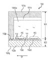
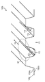
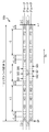
- FIG. 1A is a plan view schematically showing an external configuration of a sample storage disk 100 in the first embodiment.
- FIG. 1B is a cross-sectional view of the sample storage disk shown in FIG. 1A taken along line 1B-1B.
- FIG. 1B is a partially enlarged view of the sample storage disk 100 cut along a plane perpendicular to the disk surface and passing through the disk center Pc. Show.
- the sample storage disk 100 is used, for example, to detect red blood cells infected with malaria parasites.
- the sample storage disk 100 has a disk shape like an optical disk (CD, DVD, etc.), and a circular opening 101a is formed at the disk center Pc.
- the sample storage disk 100 includes a substrate 102 and a substrate 101 bonded to the upper surface 102p of the substrate 102.
- the substrate 101 constitutes a sample storage unit 101b. Both the substrate 101 and the substrate 102 are made of a resin material.
- the substrate 102 is made of a material that can transmit light.
- FIG. 1A By bonding the substrate 101 to the upper surface 102p of the substrate 102, nine sample accommodating portions 101b are formed as shown in FIG. 1A. These sample storage portions 101b are arranged at regular intervals in the disk circumferential direction Dc. Further, two boundaries (ends) of the sample storage unit 101b arranged in the disk circumferential direction Dc extend radially from the disk center Pc so as to be away from the disk center Pc. The nine sample storage portions 101b extend over an angular range Wa centered on the disc center Pc. As shown in FIG. 1B, the sample container 101b is a space having a predetermined height. When viewed from above, the sample storage unit 101b has a trapezoidal shape with rounded corners. The nine sample storage portions 101b have the same shape and are arranged at the same position in the disk radial direction Dr perpendicular to the disk circumferential direction Dc from the disk center Pc.
- Two holes 101c that continue to the upper surface 101p of the sample container 101b are formed on the inner peripheral side of the sample container 101b that faces the disk center Pc.
- the sample storage portion 101b is filled with the sample 100Sa from the one hole 101c.
- Sample 100Sa is prepared such that the malaria parasite in red blood cells RC is labeled with a fluorescent dye.
- the two holes 101c are closed with a lid.
- the sample 100Sa prepared from nine types of specimens is filled in the sample storage unit 101b.
- FIG. 1B schematically shows the red blood cells RC stored in the sample storage unit 101b.
- the track 102c is composed of a series of grooves 111 that spirally turn around the disk center Pc. Groove 111 is formed in the track area 102a indicated by hatching in FIG. 1A from the outermost circumference that is the outermost edge farthest from the disk center Pc of the track area 102a to the innermost circumference that is the outermost edge closest to the disk center Pc.
- the substrate 102 is formed by injection molding by the same process as that for CD and DVD.
- the semi-transmissive film 102d is formed by a sputtering process.
- the semi-transmissive film 102d reflects a part of the laser beam incident from the lower surface 102q of the substrate 102 from the lower surface 102dq of the semi-transmissive film 102d, and transmits the rest of the laser light to the semi-transmissive film 102d, thereby forming the semi-transmissive film 102d.
- the sample is guided to the sample container 101b through the upper surface 102dp.
- the semi-transmissive film 102d transmits the fluorescence generated in the sample storage portion 101b to the substrate 102 through the lower surface 102q.
- the reflectivity of the semi-transmissive film 102d is set to about 5% to 20% so that more laser light can be guided to the sample container 101b and more fluorescence can be transmitted to the substrate 102. .
- the sample storage disk 100 is divided into nine areas A0 to A8 in the disk circumferential direction Dc. Each area includes one sample container 101b. As will be described later, one track portion Ta in each area of the track 102c constitutes one unit of information recording area. Various signals are recorded in portions of the track portion Ta that do not overlap the sample storage portion 101b when viewed from above. In the present embodiment, these signals are recorded by a pit string composed of one or more pits.
- FIG. 2 is an enlarged view of the semi-transmissive film 102d located on the upper surface 102p of the substrate 102, and schematically shows the structure of the groove 111, the land 112, and the pit 113.
- FIG. 2 shows only the semipermeable membrane 102d. 2 is the substrate 102 side. That is, in FIG. 2, the upper surface 102dp of the semi-permeable membrane 102d faces downward and the lower surface 102dq faces upward.
- a groove 111 is formed on the substrate 102 (semi-transmissive film 102d).
- the lands 112 connected to the grooves 111 and between the grooves 111 constitute an upper surface 102 p of the substrate 102.
- a pit 113 is formed in a groove 111 corresponding to a portion of the track portion Ta that does not overlap the sample accommodating portion 101b, and a predetermined signal is recorded.
- the groove 111 includes pits 113 and spaces 113s. In the space 113s, the pit 113 is not formed, and the groove 111 extends monotonously. The format of the signal to be recorded will be described later. No signal is recorded on the land 112 between adjacent grooves 111. Further, the groove 111 and the land 112 extend spirally around the disc center Pc without meandering.
- the beam spot B1 of the laser beam applied to the lower surface 102q of the substrate 102 moves relatively along the groove 111 and scans the track 102c in the scanning direction Ds.
- the beam spot B1 scans the groove 111 (track 102c) from the outermost peripheral part farthest from the disk center Pc of the groove 111 toward the innermost peripheral part closest to the disk center Pc.
- the laser beam forming the beam spot B1 hits the lower surface 102dq of the semi-transmissive film 102d, a part of the laser beam is reflected by the lower surface 102q as described above and becomes reflected light.
- the intensity of the reflected light from the groove 111 decreases.
- the reflected light is modulated by the pits 113 and the intensity of the reflected light changes.
- the photodetector receives the modulated reflected light and outputs a detection signal that changes according to the intensity of the reflected light. By demodulating the detection signal, various information recorded in the pit 113 is reproduced.
- the diameter of the beam spot B1 is substantially the same as the pitch of the tracks 102c (grooves 111) extending spirally in the disc radial direction Dr, that is, the track pitch that is the interval between the track portions Ta adjacent to each other in the disc radial direction Dr. In the first embodiment, the track pitch is about 0.3 ⁇ m to 2.0 ⁇ m.
- FIG. 3A is a plan view of the sample storage disk 100, schematically showing areas A0 to A8 arranged in the disk circumferential direction Dc.
- FIG. 3B is a plan view of the sample storage disk 100.
- the track region 102a of the sample storage disk 100 is divided into a plurality of zones Z0 to Zn arranged in the disk radial direction Dr.
- FIG. 3B schematically shows a plurality of zones Z0 to Zn.
- Areas A0 to A8 shown in FIG. 3A and zones Z0 to Zn shown in FIG. 3B are logically assigned to the sample storage disk 100 in order to set a signal format to be described later on the track 102c in relation to the sample storage unit 101b. It is a thing and is not divided by physical structures, such as a barrier and a groove
- the sample storage disk 100 is divided into a plurality of areas at a predetermined constant angular interval with respect to the disc center Pc.
- nine areas are provided at an angular interval of 40 degrees with respect to the disc center Pc. It is divided into A0 to A8.
- the track portion included in each area is the track portion Ta in FIG. 1A.
- the track area 102a shown in FIG. 1A is detected between the outer area 102e farthest from the disk center Pc, the inner area 102f closest to the disk center Pc, and the outer area 102e and the inner area 102f in the disk radial direction Dr. It is divided into an area 102g.
- the outer area 102e is a lead-in area
- the inner area 102f is a lead-out area and an appearance identification area.
- the groove 111 of the lead-in area (outer area 102e), various information necessary for scanning the sample storage disk 100 is recorded in pit rows.
- a signal indicating the lead-out area is recorded as a pit string.
- the appearance identification area (inner area 102f) is provided with a structure for visually displaying the type and the like of the sample storage disk 100 by making the groove 111 discontinuous. The appearance identification area is set on the inner circumference side closer to the disk center Pc of the lead-out area.
- the detection region 102g of the sample storage disk 100 is divided into a plurality of zones Z0 to Zn in the disk radial direction Dr.
- the sample storage disk 100 is divided into, for example, 75 zones.
- the number of track portions arranged in the disk radial direction Dr included in each zone in the track 102c is the same.
- the track 102c (groove 111) of one zone is scanned by the beam spot B1 at the same angular velocity with respect to the disc center Pc.
- the angular velocity of each zone is set so that the track portion Ta of the track 102c (groove 111) at the center position of the zone in the disc radial direction Dr is scanned by the beam spot B1 at the same linear velocity.
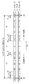
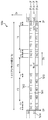
- FIG. 4 shows the groove 111 and the land 112 of each zone developed in a straight line.
- the groove 111 and the land 112 for one round are shown by one straight line.
- the lengths of the grooves 111 and lands 112 shown in FIG. 4 are not physical lengths, but are standardized so that the length of one round is the same in all the grooves 111 and lands 112 for convenience. Has been.
- the detection area 102g is divided into a plurality of zones Z0 to Zn in the disk radial direction Dr.
- Each zone includes a plurality of tracks 102c (grooves 111) arranged in the disk radial direction Dr.
- track numbers T0 to Tm from the outer peripheral side are given to the track portion Ta of the track 102c in one zone.
- the number of track portions Ta of the track 102c included in one zone is, for example, 800.
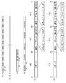
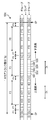
- FIG. 5A shows a format of fields F1 to F9 set in each of a plurality of track portions Ta (groove 111) in each area Ax of areas A0 to A8.
- FIG. 5B schematically shows the angle range of the fields F1 to F9.
- fields F1 to F9 are set in each of a plurality of track portions Ta (groove 111) in one area Ax.
- the fields F2, F5, and F7 no signal is recorded in the pit 113 (see FIG. 2), and only the groove 111 (G) including only the monotonically extending space 113s (see FIG. 2) is formed.
- the field F5 overlaps the sample storage portion 101b in the entire length. That is, both ends of the field F5 coincide with two boundaries (ends) arranged in the disk circumferential direction Dc of the sample storage unit 101b. Therefore, no signal is recorded on the track portion that overlaps the sample storage portion 101b when viewed from above, and only the groove 111 that extends monotonously and flat is formed.
- the track portion Ta starts at the start end SP and ends at the end EP along the scanning direction Ds.
- the start ends SP of all track portions Ta within the same area are aligned in one disk radial direction Dr1, that is, located on a straight line Lr1 extending from the disk center Pc in the disk radial direction Dr1.
- the end points EP of all track portions Ta in the same area are aligned in one disc radial direction Dr, that is, located on a straight line Lr2 extending from the disc center Pc in the disc radial direction Dr2.
- the start ends of the fields F5 in all the track portions Ta in the same area are aligned in the disc radial direction Dr, and the end ends of the field F5 are aligned in another disc radial direction Dr.
- the start ends of the field F1 in all the track portions Ta in the same area are aligned in another disk radial direction Dr, and the ends of the field F1 are aligned in another disk radial direction Dr.
- the start ends of the field F3 in all the track portions Ta in the same area are aligned in another disk radial direction Dr, and the ends of the field F3 are aligned in another disk radial direction Dr.
- the start ends of the fields F4 in all track portions Ta in the same area are aligned in another disk radial direction Dr, and the ends of the field F4 are aligned in another disk radial direction Dr.
- the start ends of the fields F6 in all the track portions Ta in the same area are aligned in another disk radial direction Dr, and the ends of the field F6 are aligned in another disk radial direction Dr.
- the start ends of the field F8 in all the track portions Ta in the same area are aligned in another disk radial direction Dr, and the ends of the field F8 are aligned in another disk radial direction Dr.
- the start ends of the fields F9 in all the track portions Ta in the same area are aligned in another disk radial direction Dr, and the ends of the field F9 are aligned in another disk radial direction Dr.
- FIG. 6A shows a signal format of the fields F1 to F9 of a certain track portion Ta1 among the plurality of track portions Ta.
- Each of the plurality of track portions Ta has the same configuration as the track portion Ta1.
- a hatched portion indicates a region where the pit 113 is formed in the groove 111, and a white portion where the hatched hatch is not illustrated indicates a region of only the groove 111 where the pit 113 is not formed.
- the time length 1T indicates the time length of the minimum pit when the groove 111 is scanned at a constant angular velocity as described above.
- a signal En composed of pits and spaces that are alternately repeated 10 times is recorded. Both the pit and the space of the signal En have a time length 2T that is twice the time length 1T.
- the signal En recorded in the field F1 indicates the start point SP (see FIG. 5A) of the track portion Ta1 of one area, and the signal En recorded in the field F9 is the end point EP of the track portion Ta1 of one area (see FIG. 5A). ).
- the pits 113 are not formed in the fields F2, F5, and F7, and the fields F2, F5, and F7 are composed of only the space 113s.
- Field F4 starts with a space having a time length 8T which is eight times the time length 1T, a pit having a time length 1T and a space having a time length 1T which are alternately repeated four times after the space.
- a signal V3 is recorded.
- the start signal V3 indicates a position where the sample storage unit 101b starts in the scanning direction Ds.
- an end signal Vs composed of repeated pits and spaces alternately 5 times is recorded. Both the pit and space of the end signal Vs have a time length 4T that is four times the time length 1T.
- the end signal Vs indicates a position where the sample storage unit 101b ends along the scanning direction Ds.
- the field F3 is composed of three header areas HE0 to HE2.
- the header area HE0 is a reserved area in which an arbitrary signal not defined by the format can be recorded.
- an identification signal for identifying the header area HE1 an address signal indicating the position of the track portion Ta1, and an error correction signal for performing error detection or error correction on the address signal are recorded. These signals have a fixed bit length.
- the address signal includes the track number of the track portion Ta1 of the track numbers T0 to Tm shown in FIG. 4, the zone number indicating the zone including the track portion Ta1 of the zones Z0 to Zn, and the areas A0 to A9. And an area number indicating an area including the track portion Ta1.
- signals similar to those in the header area HE1 are recorded.
- the field F8 includes three footer areas FT0 to FT2.
- the footer area FT0 is a reserved area like the header area HE0.
- an identification signal, an address signal, and an error correction signal are recorded. These signals have a fixed bit length.
- the address signal includes the track number of the track portion Ta1 of the track numbers T0 to Tm, the zone number indicating the zone including the track portion Ta1 of the zones Z0 to Zn, and the track portion Ta1 of the areas A0 to A9.
- the area number indicating the area to be included is included.
- a signal similar to that in the footer area FT1 is recorded.
- the identification signals in the footer areas FT1 and FT2 are different from the identification signals in the header areas HE1 and HE2.
- the address signals in the footer areas FT1 and FT2 are the same as the address signals in the header areas HE1 and HE2.
- digital signals (bit signals) having values of 1 and 0 are recorded depending on pits and spaces.
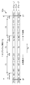
- FIG. 6B is a schematic enlarged view of the sample storage disk 100, and shows a field F4 in a track portion Ta of track numbers T11 to T15. As shown in FIG.
- a space Sc1 having a time length 8T, a pit Pt1 having a time length 1T, and a space Sc2 having a time length 1T along the scanning direction Ds A pit Pt2 having a time length 1T, a space Sc3 having a time length 1T, a pit Pt3 having a time length 1T, a space Sc4 having a time length 1T, a pit Pt4 having a time length 1T, and a time length 1T Space Sc5 is arranged in this order. As shown in FIG.
- both ends of the space Sc1 of the field F4 in all the track portions Ta of each zone including the track numbers T11 to T15 are aligned in the disk radial directions Dr11 and Dr12 that are separated from the disk center Pc. And located on straight lines Lr11 and Lr12 extending in the disk radial direction Dr11 and Dr12 from the disk center Pc, respectively.
- Both ends of the pit Pt1 of the field F4 of all the track portions Ta of each zone of each area including the track numbers T11 to T15 are aligned in the disk radial directions Dr12 and Dr13 away from the disk center Pc, and the disk diameter from the disk center Pc. They are located on straight lines Lr12 and Lr13 extending in directions Dr12 and Dr13, respectively.
- Both ends of the space Sc2 of the field F4 of all track portions Ta of each zone of each area including the track numbers T11 to T15 are aligned in the disk radial directions Dr13 and Dr14 away from the disk center Pc, and the disk diameter from the disk center Pc. They are located on straight lines Lr13 and Lr14 extending in directions Dr13 and Dr14, respectively. Both ends of the pit Pt2 of the field F4 of all track portions Ta of each zone of each area including the track numbers T11 to T15 are aligned in the disk radial directions Dr14 and Dr15 away from the disk center Pc, respectively. They are located on straight lines Lr14 and Lr15 extending in directions Dr14 and Dr15, respectively.
- Both ends of the space Sc3 of the field F4 of all track portions Ta of each zone of each area including the track numbers T11 to T15 are aligned in the disk radial directions Dr15 and Dr16 away from the disk center Pc, and the disk diameter from the disk center Pc. They are located on straight lines Lr15 and Lr16 extending in the directions Dr15 and Dr16, respectively.
- Both ends of the pit Pt3 of the field F4 of all track portions Ta of each zone of each area including the track numbers T11 to T15 are aligned in the disc radial directions Dr16 and Dr17, respectively, away from the disc center Pc. They are located on straight lines Lr16 and Lr17 extending in directions Dr16 and Dr17, respectively.
- Both ends of the space Sc4 of the field F4 of all the track portions Ta of each zone of each area including the track numbers T11 to T15 are aligned in the disk radial directions Dr17 and Dr18 away from the disk center Pc. They are located on straight lines Lr17 and Lr18 extending in the directions Dr17 and Dr18, respectively. Both ends of the pit Pt4 of the field F4 of all track portions Ta of each zone of each area including the track numbers T11 to T15 are aligned in the disc radial directions Dr18 and Dr19, respectively, away from the disc center Pc. They are located on straight lines Lr18 and Lr19 extending in directions Dr18 and Dr19, respectively.
- Both ends of the space Sc5 of the field F4 of all the track portions Ta of each zone of each area including the track numbers T11 to T15 are aligned in the disk radial directions Dr19 and Dr110 that are separated from the disk center Pc, and the disk diameter from the disk center Pc. They are located on straight lines Lr19 and Lr110 extending in directions Dr19 and Dr110, respectively.
- the pits and spaces formed in the fields F1 and F9 are aligned in the disc radial direction Dr in the track portion Ta included in all the zones of the same area. Since the pits and spaces formed in the fields F3 and F8 have different time lengths depending on the contents of the address signal, the positions of the pits and spaces in the plurality of track portions Ta are shifted in the disk circumferential direction Dc.
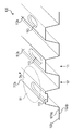
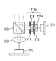
- FIG. 7 is a configuration diagram of a fluorescence detection pickup 200 for reading fluorescence from the sample storage disk 100.
- fluorescence is detected from the sample storage portion 101 b of the sample storage disk 100 using the fluorescence detection pickup 200.
- fluorescence is detected from the sample storage disk 100 to determine whether the red blood cells RC are infected with malaria parasites.
- the sample 100Sa is prepared so that the malaria parasite in the red blood cells RC is labeled with a fluorescent dye.
- the fluorescent dye when the fluorescent dye is irradiated with light having a wavelength of 405 nm, the fluorescent dye generates fluorescence having a wavelength of about 450 to 540 nm.
- the sample 100Sa thus prepared is filled into the nine sample storage portions 101b of the sample storage disk 100 for each specimen. Thereafter, the opening 101a (see FIG. 1A) of the sample storage disk 100 is fixed to the turntable 230 supported by the spindle motor 220.
- the fluorescence detection pickup 200 includes a semiconductor laser 201, a half-wave plate 202, a polarizing beam splitter (PBS) 203, a collimator lens 204, a quarter-wave plate 205, an objective lens 206, and an objective lens actuator. 207, a dichroic prism 208, an anamorphic lens 209, a photodetector 210, and a fluorescence detector 211.
- PBS polarizing beam splitter
- the semiconductor laser 201 emits a laser beam having a wavelength of about 405 nm.
- the polarization direction of the laser light emitted from the semiconductor laser 201 is adjusted by the half-wave plate 202 so as to be S-polarized with respect to the PBS 203.
- the laser beam is reflected by the PBS 203 and enters the collimator lens 204.
- the PBS 203 has polarization dependency of characteristics such as reflection and transmission only for light near the wavelength of the laser light emitted from the semiconductor laser 201, and has a wavelength other than the wavelength of the laser light, for example, a wavelength of about 450 to 540 nm. Light does not have polarization dependency of the above characteristics.
- the collimator lens 204 converts laser light incident from the PBS 203 side into parallel light.
- the quarter-wave plate 205 converts the laser light incident from the collimator lens 204 side into circularly polarized light, and the polarization direction when the laser light incident from the objective lens 206 side is incident from the collimator lens 204 side.
- the laser light reflected by the semi-transmissive film 102d of the sample storage disk 100 passes through the PBS 203 as it is and is not reflected toward the fluorescence detector 211.
- the objective lens 206 converges the laser light incident from the 1 ⁇ 4 wavelength plate 205 side on the semi-transmissive film 102d of the sample storage disk 100.
- the objective lens actuator 207 is displaced by driving the objective lens 206 in the focus direction and the tracking direction so that the laser beam converges on the groove 111 of the sample storage disk 100 by a servo circuit 50 (see FIG. 9) described later.
- the dichroic prism 208 transmits light having a wavelength of about 405 nm of the laser light emitted from the semiconductor laser 201 and reflects light having a fluorescence wavelength other than the wavelength of the laser light emitted from the semiconductor laser 201, for example, about 450 to 540 nm. It is configured as follows. As a result, the fluorescence incident from the PBS 203 side is reflected by the dichroic prism 208, and the laser light incident from the PBS 203 side passes through the dichroic prism 208.
- the anamorphic lens 209 introduces astigmatism into the laser light transmitted through the dichroic prism 208.
- the laser light that has passed through the anamorphic lens 209 enters the photodetector 210.
- the photodetector 210 has a four-divided sensor for receiving laser light on the light receiving surface.
- the detection signal output from the photodetector 210 is processed by a signal arithmetic circuit 300 (see FIG. 8) described later.
- the fluorescence reflected by the dichroic prism 208 is guided to the light receiving surface of the fluorescence detector 211 while being converged by the collimator lens 204.
- the fluorescence detector 211 has a sensor for receiving fluorescence by being provided on the light receiving surface.
- the detection signal of the fluorescence detector 211 is amplified by a signal amplification circuit.
- a barrier for preventing the laser light emitted from the semiconductor laser 201 from entering the fluorescence detector 211 is optically appropriately used. It is preferable to arrange in the system.
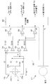
- FIG. 8 is a configuration diagram of the signal arithmetic circuit 300 according to the first embodiment.
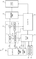
- FIG. 9 is a configuration diagram of the fluorescence detection apparatus 1 according to the first embodiment.
- the light detector 210 has a quadrant sensor for receiving laser light as described above.
- the upper left sensor 2101, the upper right sensor 2102, the lower right sensor 2103, and the lower left sensor 2104 of the quadrant sensor output detection signals S1, S2, S3, and S4 based on the beam spot of the received laser beam, respectively.
- the signal arithmetic circuit 300 processes the detection signals S1 to S4 to generate a focus error signal FE, a tracking error signal TE, and a reproduction RF signal RF.
- the focus error signal FE and the tracking error signal TE are generated according to the astigmatism method and the one-beam push-pull method used in existing optical disc apparatuses.
- the signal operation circuit 300 includes adders 301 to 304 and 307 and subtractors 305 and 306.
- the adder 301 outputs a signal (S1 + S3) obtained by adding the detection signals S1 and S3 to the subtractor 305
- the adder 302 outputs a signal (S2 + S4) obtained by adding the detection signals S2 and S4 to the subtractor 305.
- the adder 303 outputs a signal (S1 + S4) obtained by adding the detection signals S1 and S4 to the subtractor 306 and the adder 307
- the adder 304 adds the signal (S2 + S3) obtained by adding the detection signals S2 and S3 to the subtractor 306. And output to the adder 307.
- the subtracter 305 subtracts the output signal of the adder 302 from the output signal of the adder 301 and outputs a focus error signal FE.
- the subtracter 306 subtracts the output signal of the adder 304 from the output signal of the adder 303 and outputs a tracking error signal TE.
- the adder 307 adds the output signals of the adders 303 and 304 and outputs a reproduction RF signal RF (SUM signal).
- the focal position of the objective lens 206 when the focal position of the objective lens 206 is positioned on the semi-transmissive film 102d of the sample storage disk 100, the beam spot on the four-divided sensors 2101 to 2104 of the photodetector 210 becomes a minimum circle of confusion, and a focus error signal.
- the value of FE becomes 0.
- the focal position of the objective lens 206 is positioned at the center position in the disk radial direction Dr of the track 102c (groove 111) of the sample storage disk 100, the beam spots on the quadrant sensors 2101 to 2104 of the photodetector 210.
- the size of the portion applied to the left two sensors 2101 and 2104 is equal to the size of the portion applied to the two right sensors 2102 and 2103, and the value of the tracking error signal TE is zero.
- the objective lens actuator 207 shown in FIG. 7 has the objective lens 206 mounted on the substrate of the sample storage disk 100 so that both the focus error signal FE and the tracking error signal TE become zero under the control of the servo circuit 50 shown in FIG. Driving is performed in a focus direction perpendicular to the upper surface 102p of the substrate 102 and a tracking direction parallel to the upper surface 102p of the substrate 102.
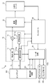
- the fluorescence detection apparatus 1 includes a signal processing circuit 10, an image processing unit 20, an input / output unit 30, a controller 40, and a servo.
- a circuit 50 and a thread motor 240 are provided.
- the signal operation circuit 300 in FIG. 8 is provided in the fluorescence detection pickup 200.
- the signal processing circuit 10 of the fluorescence detection apparatus 1 processes the fluorescence signal FL and the reproduction RF signal RF output from the fluorescence detection pickup 200.
- the fluorescence signal is output from the fluorescence detector 211 in FIG. 7, and the reproduction RF signal RF is output from the adder 307 in FIG.
- the signal processing circuit 10 includes a signal detection unit 11, a signal reproduction unit 12, a cutout unit 13, and a superposition unit 14.
- the signal detection unit 11 and the signal reproduction unit 12 constitute a signal acquisition unit 11a.
- the signal detection unit 11 processes the reproduction RF signal RF input from the fluorescence detection pickup 200, detects various signals shown in FIG. 6A, and sends the detected signals to the signal reproduction unit 12, the cutout unit 13, and the controller 40. Output.
- the signal reproduction unit 12 reproduces the signals in the fields F3 and F8 input from the signal detection unit 11, that is, the signals in the header areas HE0 to HE2 and the footer areas FT0 to FT2, and acquires an address signal.
- the signal reproducing unit 12 outputs the acquired address signal to the superimposing unit 14.
- the cutout unit 13 converts each sample value obtained by sampling the fluorescence signal input from the fluorescence detection pickup 200 with a sampling clock of a predetermined period into a digital signal and outputs the digital signal to the superimposition unit 14.
- the cutout unit 13 ends the sampling of the fluorescence signal FLd in response to detection of the start signal V3 (see FIG. 5A) by the signal detection unit 11.
- the sample storage disk 100 is rotated at a different angular velocity for each zone. Accordingly, the time during which the track portion Ta is scanned with the laser light varies from zone to zone. For this reason, when a fluorescence signal is cut out with a timing signal having the same period for each zone, the number of cut out signal groups differs for each zone.
- the period of the sampling clock in the cutout unit 13 is adjusted so that the same number of signal groups are cut out from the track portion Ta of each zone. Thereby, in each zone, the fluorescence signal FL is cut out at substantially the same angular interval.
- the superimposing unit 14 adds the address signal input from the signal reproducing unit 12 to the fluorescence signal acquired by the clipping unit 13 and outputs the signal to the image processing unit 20.
- the image processing unit 20 connects the input fluorescent signals to generate a fluorescent image for each of the areas A0 to A8.
- the image processing unit 20 performs image processing on the fluorescent image, counts the number of fluorescent bright spots, and calculates the infection rate of malaria in the red blood cells RC. These fluorescent images, count values, infection rates, and the like are output from the image processing unit 20 to the input / output unit 30 as needed.
- the controller 40 controls the servo circuit 50 and the signal processing circuit 10 so that the period from the start signal V3 in which the address signal has changed to the end signal Vs is scanned again with the laser light and the fluorescent signal is extracted.
- the input / output unit 30 includes input devices such as a keyboard, a mouse, and a touch panel, and output devices such as a monitor and a speaker.
- An instruction for starting fluorescence detection is input via the input / output unit 30.
- the fluorescence image, the number of bright spots, the infection rate of malaria, and the like are displayed on the input / output unit 30.
- a method of obtaining a fluorescent image of the entire flow path by staining the cells to be detected with a fluorescent dye and storing them in the flow path can be used.
- the presence / absence and number of detection target cells can be acquired by analyzing the acquired fluorescence image, and based on this, the infection rate of pathogenic bacteria and the like can be acquired. It is also possible to display the acquired fluorescence image as appropriate and visually confirm the occurrence of fluorescence.
- the controller 40 includes a processing circuit such as a CPU (Central Processing Unit) and a memory such as a ROM (Read Only Memory) and a RAM (Random Access Memory), and controls each unit according to a program stored in the memory.
- a processing circuit such as a CPU (Central Processing Unit) and a memory such as a ROM (Read Only Memory) and a RAM (Random Access Memory), and controls each unit according to a program stored in the memory.
- the servo circuit 50 controls the objective lens actuator 207 based on the focus error signal FE and the tracking error signal TE generated by the signal calculation circuit 300 in FIG.
- the servo circuit 50 controls the spindle motor 220 so that the zones Z0 to Zn shown in FIG. 3B are scanned by the beam spot B1 at the angular velocity set in each zone.
- the servo circuit 50 is a thread for sending the fluorescence detection pickup 200 in the disk radial direction Dr of the sample storage disk 100 so that the beam spot B1 can be scanned from the outermost position to the innermost position of the track 102c.
- the motor 240 is controlled.
- the servo circuit 50, the fluorescence detection pickup 200, the spindle motor 220, and the sled motor 240 constitute a scanning unit 1200 that irradiates the sample storage disk 100 with light and scans the sample storage disk 100 in the scanning direction Ds.
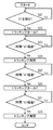
- FIG. 10A is a flowchart showing an address signal acquisition process.
- the signal reproduction unit 12 acquires a signal in the header region HE1 from the signal detection unit 11 (S11), and applies an error correction signal to the address signal in the acquired signal to perform error correction processing (S12). If the error correction process is appropriate (S13: YES), the signal reproduction unit 12 does not perform the address signal reproduction process on the header region HE2, and uses the address signal acquired by the error correction process in the field F3 (FIG. 5A). Reference) address signal (S14), and the process ends. On the other hand, if the error correction processing is not appropriate (S13: NO), the signal reproduction unit 12 further acquires a signal in the header area HE2 (S15), and applies an error correction signal to the address signal in the acquired signal to generate an error. Correction processing is performed (S16). If the error correction process is appropriate (S17: YES), the signal reproduction unit 12 acquires the address signal acquired by the error correction process as the address signal of the field F3 (see FIG. 5A) (S18), and performs the process. finish.
- steps S12 and S16 error detection processing and error correction processing are performed using the error correction signals included in the header areas HE1 and HE2. If no error is detected in the address signal, it is determined that the address signals included in the header areas HE1 and HE2 are appropriate. When an error is detected, an error bit in the address signal is extracted by an operation using the error correction signal, and the error bit is corrected. If the determination in step S17 is NO, the controller 40 scans the track portion Ta again.
- the address signal acquisition process for the footer areas FT1 and FT2 is performed in the same manner as the address signal acquisition process for the header areas HE1 and HE2 shown in FIG. 10A. That is, in the address signal acquisition process for the footer areas FT1 and FT2, the processing steps S11 and S12 for acquiring the signals of the header areas HE1 and HE2 in FIG. 10A are replaced with processes for acquiring the signals of the footer areas FT1 and FT2, respectively. It is done.
- the address signal since the address signal is recorded in each of the header areas HE1 and HE2, the address signal can be acquired from the header area HE2 even when the address signal cannot be properly read from the header area HE1. .
- FIG. 10B is a flowchart showing tracking control.
- the servo circuit 50 maintains the tracking servo signal at the previous signal value (S22) and waits for the time Ts1 to elapse. (S23).
- the time Ts1 is set to a time required for the beam spot B1 to pass through the start end of the field F5. Since the starting end of the field F5 is located at the boundary (end) of the sample storage unit 101b, the reflectance of the laser beam changes greatly at this position, and the tracking error signal is easily disturbed. When the tracking error signal is disturbed, there is a possibility that the scanning position of the beam spot B1 is shifted from the target track to an adjacent track or the like.
- the tracking servo signal is maintained at the previous signal value until the beam spot B1 passes through the beginning of the field F5, that is, until the time Ts1 elapses (S22). It prevents it from coming off. Thereby, the track 102c can be stably scanned with the laser beam.
- the servo circuit 50 resumes tracking servo (S24). Thereafter, when the time Ts2 elapses (S25: YES), the servo circuit 50 again maintains the tracking servo signal at the previous signal value (S26), and waits for the time Ts3 to elapse (S27). When the time Ts3 has elapsed (S27: YES), the servo circuit 50 resumes tracking servo (S28).
- the time Ts2 is set to the time required for the beam spot B1 to reach the position immediately before the end of the field F5.
- the time Ts3 is set to the time required for the beam spot B1 to pass through the end of the field F5 from the position immediately before the end of the field F5.
- the purpose of maintaining the tracking servo signal near the end of the field F5 in the processing of steps S25 to S27 and the effect thereof are the purpose of maintaining the tracking servo signal near the start of the field F5 in the processing of steps S22 to S23 and The effect is the same. That is, this process also takes into consideration that the reflectance of the laser beam changes greatly at the end of the field F5 and the tracking error signal is likely to be greatly disturbed. By these processes, the track 102c can be stably scanned, and as a result, the fluorescence signal extraction process can be smoothly advanced.
- step S27 it is determined that the time Ts3 to reach the end of the field F5 has elapsed, but a predetermined signal is further recorded before the end of the field F5, and the process is performed by detecting this signal. You may move to.
- FIG. 11A is a flowchart showing a cutting process for cutting out a fluorescent signal.
- the extraction unit 13 starts extraction (sampling) of the fluorescence signal (S32). Thereafter, when the signal detection unit 11 detects the end signal Vs (see FIG. 5A) (S33: YES), the extraction unit 13 ends the extraction (sampling) of the fluorescence signal (S34).
- the controller 40 may control the cutout unit 13 so that the cutout unit 13 starts to cut out the fluorescence signal later.
- the extraction of the fluorescence signal ends in response to the detection of the end signal Vs.
- the extraction unit 13 outputs the fluorescence signal at the timing immediately before the end of the field F5.
- the controller 40 may control the cutting unit 13 so that the cutting is finished.
- FIG. 11B is a flowchart showing invalidation processing for invalidating the cut-out signal.
- the controller 40 acquires the address signal reproduced from the header areas HE1 and HE2 while scanning one track portion Ta (S41), and acquires the address signal reproduced from the footer areas FT1 and FT2 (S42). .
- the controller 40 determines whether or not the two address signals acquired in this way match (S43). If the two address signals do not match (S43: No), the controller 40 invalidates the fluorescence signal cut out from the track portion Ta (S44), scans the track portion Ta again with laser light, and outputs the fluorescence signal.
- the cutting unit 13 is controlled so as to cut out (S45). When the two address signals match (S43: Yes), the controller 40 ends the process without invalidating the fluorescent signal cut out from the track portion Ta.
- the laser beam spot B1 may have moved out of the groove 111 and moved to another groove while scanning the groove 111 overlapping the sample storage unit 101b. .
- the fluorescence signal cut out in the meantime is acquired across two track portions, and is not a fluorescence signal acquired from one track portion.
- the fluorescence detection apparatus 1 while the process of FIG. 11B is executed and the groove 111 that overlaps the sample storage unit 101b is scanned, the beam spot B1 of the laser beam is separated from the groove 111 and moves to another groove. If there is a possibility of movement, the fluorescence signal acquired during that time is invalidated and the fluorescence signal is cut out again. Thereby, a fluorescence signal is appropriately acquired from one track portion Ta.
- FIG. 12 is a diagram for explaining the fluorescence signal cutting process.
- the cutout unit 13 samples the fluorescence signal output from the fluorescence detection pickup 200 in synchronization with the sampling clock Sck with a certain period while the laser beam scans the field F5, and acquires the sample value at each timing.
- FIG. 12 schematically shows the sampling clock Sck and signals cut out from one group of track portions Ta (track numbers T0 to Tm) included in the same area in the same zone.
- k signals SP1 to SPk are obtained from one track portion Ta.
- red blood cells RC infected with malaria are present in the sample at the timing when the signal SP5 is scanned while the track portion Ta of the track number T1 is scanned with the laser beam.
- the sampling value of the signal SP5 of the track number T1 is higher than the other signals SP1 to SP4 and SP6 to SPk of the track number T1 and the signals SP1 to SPk of the other tracks (track numbers T0, T2 to Tm).
- Sample values of signals around signal SP5 are larger than those of signals SP5 of signals SP4 to SP6 and the surrounding signals. It is high.
- the higher the sample value the higher the hatching density.
- the image processing unit 20 in FIG. 9 performs the scanning order and track number of signals of one group of track portions Ta included in the same area in the same zone based on the signal and address signal input from the superimposing unit 14. Are arranged in this order to generate a fluorescence image showing one sample storage unit 101b.
- the image processing unit 20 analyzes the fluorescence image thus generated, counts the number of fluorescent bright spots, that is, the number of red blood cells RC infected with malaria, and based on the number, malaria of red blood cells RC contained in the sample 100Sa. Calculate the infection rate.
- the image processing unit 20 outputs the acquired count value and infection rate to the input / output unit 30 together with the fluorescent image. As a result, the fluorescence image, the number of detected malaria, the malaria infection rate, and the like are displayed on the input / output unit 30.
- the sample container 101b is arranged so that two boundaries (ends) in the disk circumferential direction Dc extend radially from the disk center Pc. For this reason, when the sample storage disk 100 is rotated at a constant angular velocity, the range of the sample storage portion 101b is scanned when a laser beam is used to scan an arbitrary track portion Ta that overlaps one sample storage portion 101b as viewed from above. The period of time is substantially constant. Thereby, in the fluorescence detection device 1 as described above, the start signal V3 and the end signal Vs (see FIG.
- the fluorescent signal is sampled and cut out at a predetermined interval. Accordingly, a series of fluorescent image fragments along one track portion Ta can be acquired from the sample 100Sa accommodated in the sample accommodating portion 101b. The fragments acquired in this manner are joined together as shown in FIG. 12, whereby a fluorescence image of the entire sample storage unit 101b can be acquired.
- a header region HE1, HE2 and a footer region FT1, FT2 are provided upstream and downstream of the sample storage portion 101b in the scanning direction of the track 102c, respectively. Is set.
- address signals having the same contents are recorded in the header areas HE1 and HE2 and the footer areas FT1 and FT2, respectively.
- the sample storage disk 100 is divided into areas A0 to A8 in the disk circumferential direction Dc.
- Two boundaries (ends) in the disk circumferential direction Dc of each area extend radially from the disk center Pc in the disk radial direction Dr. That is, the two boundaries B01 and B80 aligned in the disk circumferential direction Dc of the area A0 extend in the disk radial direction Dr away from the disk center Pc.
- the two boundaries B01 and B12 aligned in the disk circumferential direction Dc of the area A1 extend in the disk radial direction Dr away from the disk center Pc.
- Two boundaries B12 and B23 aligned in the disk circumferential direction Dc of the area A2 extend in the disk radial direction Dr away from the disk center Pc.
- Two boundaries B23 and B34 aligned in the disk circumferential direction Dc of the area A3 extend in the disk radial direction Dr away from the disk center Pc.
- Two boundaries B34 and B45 aligned in the disk circumferential direction Dc of the area A4 extend in the disk radial direction Dr away from the disk center Pc.
- Two boundaries B45 and B56 aligned in the disk circumferential direction Dc of the area A5 extend in the disk radial direction Dr away from the disk center Pc.
- Two boundaries B56 and B67 aligned in the disk circumferential direction Dc of the area A6 extend in the disk radial direction Dr away from the disk center Pc.
- Two boundaries B67 and B78 aligned in the disk circumferential direction Dc of the area A7 extend in the disk radial direction Dr away from the disk center Pc.
- Two boundaries B78 and B80 arranged in the disk circumferential direction Dc of the area A8 extend in the disk radial direction Dr away from the disk center Pc.
- Sample storage portions 101b are arranged in the areas A0 to A8, respectively, and the track portion Ta included in each area straddles the sample storage portion 101b. Thereby, when the sample storage disk 100 is rotated at a constant angular velocity, the track portions Ta included in each area are all scanned with the same time length. Therefore, the same signal format can be applied uniformly to all track portions Ta.
- the angular ranges of the areas A0 to A8 in the disk circumferential direction Dc with respect to the disk center Pc are set to be equal to each other. Therefore, the fluorescence signal can be cut out from all the areas A0 to A8 by the same processing.
- the sample storage disk 100 is divided into a plurality of zones Z0 to Zn in the disk radial direction Dr, and signals are recorded at a constant angular velocity in the track portion Ta of each zone.
- the angular velocities of the zones Z0 to Zn are set so that the linear velocities of the track portions Ta at the center position in the disk radial direction Dr of each zone are the same.
- the difference between the linear velocity on the inner periphery side of the disc and the linear velocity on the outer periphery side of the disc can be suppressed.
- the track portion Ta includes a signal indicating a zone including the track portion Ta, a signal indicating the position (track number) of the track portion in the disk radial direction Dr in the zone, A signal indicating the position (area) of the track portion Ta in the disk circumferential direction Dc is recorded as an address signal.
- the sample storage disk 100 that stores the sample 100Sa is disposed above the substrate 102, the track 102c formed on the upper surface 102p of the substrate 102 so as to turn around the disk center Pc, and the track 102c. And one or more sample storage portions 101b for storing the sample 100Sa.
- the track 102c is configured to be scanned in the scanning direction Ds.
- Each of the plurality of track portions Ta straddling each sample storage portion 101b of the one or more sample storage portions 101b in the track 102c is upstream of each sample storage portion 101b in the scanning direction Ds of each track portion Ta.
- An address signal indicating the position of the track portion Ta is recorded.
- Another address signal indicating the position of each track portion Ta is recorded on the downstream side of each sample storage portion 101b in the scanning direction Ds of each track portion Ta.
- a plurality of start signals V3 indicating the start of the respective sample storage portions 101b in the scanning direction Ds are upstream from the respective sample storage portions 101b in the scanning direction Ds of the plurality of track portions Ta. May be recorded so as to be aligned with each other.
- a plurality of end signals Vs indicating the end of each sample storage portion 101b in the scanning direction Ds are separated from the disc center Pc. It may be recorded so as to be aligned in the direction Dr.
- the area of the sample storage disk (track area 102a) on which the track 102c is formed extends in the disk circumferential direction Dc perpendicular to the plurality of disk radial directions Dr at a plurality of boundaries extending in the plurality of disk radial directions Dr away from the disk center Pc. It may be divided into a plurality of arranged areas A0 to A8. A plurality of sample storage portions 101b are respectively arranged in the plurality of areas A0 to A8.
- the plurality of areas A0 to A8 may be arranged within the same angular range from the disc center Pc.
- the portions of the plurality of track portions Ta that overlap one or more sample storage portions 101b as viewed from above may be monotonously extended without signals being recorded.
- the synchronization adjustment signals may be recorded in at least one of the portions of the plurality of track portions Ta that overlap one or more sample storage portions 101b as viewed from above.
- the plurality of track portions Ta may be arranged in the disc radial direction Dr away from the disc center Pc. Even if the plurality of signals En indicating the start ends SP at which the plurality of track portions Ta start in the scanning direction Ds are arranged in another disc radial direction Dr away from the disc center Pc, they are recorded at the start ends SP of the plurality of track portions Ta. Good. A plurality of signals En indicating end EPs at which the plurality of track portions Ta end in the scanning direction Ds are recorded at the end EPs of the plurality of track portions Ta so as to be arranged in another disc radial direction Dr away from the disc center Pc. Also good.
- the sample storage disk 100 may be divided into a plurality of zones Z0 to Zn along the disk radial direction Dr away from the disk center Pc.
- a plurality of groups of track portions Ta among the plurality of track portions Ta are respectively arranged in the plurality of zones Z0 to Zn.
- a signal may be recorded at a constant angular velocity on each track portion Ta of the plurality of track portions.
- the constant angular velocity is set so that the linear velocity of the track portion Ta at the center position in the disk radial direction Dr of the track portions Ta of each group becomes a predetermined linear velocity in the track portions Ta of the plurality of groups. It may be.
- Each of the two address signals includes a signal indicating a zone including each track portion Ta among the plurality of zones Z0 to Zn, and a signal indicating a position of each track portion Ta in the zone in the disk radial direction Dr. , And a signal indicating the position of each track portion Ta in the disk circumferential direction Dc perpendicular to the disk radial direction Dr and surrounding the disk center Pc.
- the address signal is recorded by a pit row composed of a plurality of pits 113 formed on the track 102c.
- the two boundaries arranged in the disk circumferential direction Dc surrounding the disk center Pc of the one or more sample storage units 100b may extend radially from the disk center Oc.
- the fluorescence detection apparatus 1 includes a scanning unit 1200 that irradiates the sample storage disk 100 with light and scans the sample storage disk 100 in the scanning direction Ds, and a light detection that outputs a detection signal according to the light reflected by the sample storage disk 100.
- a signal acquisition unit 11a that operates according to the detection signal
- a fluorescence detector 211 that outputs a fluorescence signal corresponding to the fluorescence generated from the sample 100Sa accommodated in the sample accommodation unit 101b by the irradiated light
- a cutout unit 13 that samples and cuts out the fluorescent signal
- a controller 40 that controls processing of the cut out fluorescent signal are provided.
- the signal acquisition unit 11a acquires two address signals based on the signal output from the photodetector 210. Based on the two address signals acquired by the signal acquisition unit 11a, the controller 40 controls the above processing on the cut-out fluorescence signal.
- FIG. 13 is a diagram in which grooves and lands in each zone of the sample storage disk 100a according to the second embodiment are developed in a straight line.
- the same reference numerals are assigned to the same parts as those of the sample storage disk 100 in the first embodiment shown in FIGS. 1A to 6A.
- the groove 111 extends spirally from the outermost periphery to the innermost periphery.
- the groove 111 and the land 112 are alternately replaced each time the area is switched in the disk circumferential direction Dc. Yes.
- the track area 102a of the sample storage disk 100a is divided into nine areas A0 to A8 in the disk circumferential direction Dc. Therefore, when the track 102 c starting from the groove 111 makes one round, the next one track 102 c starts from the land 112.
- the groove 111 and the land 112 are alternately repeated in the disk radial direction Dr.
- the number of track portions Ta of each zone is set so that the track 102c of the track number T0 of all zones starts from the groove 111.
- the number of tracks 102c (track portions Ta) included in one zone is, for example, 1600, which is twice that of the sample storage disk 100 in the first embodiment.
- the sample storage disk 100 In the sample storage disk 100 according to the first embodiment, only the groove 111 is scanned with laser light.
- the sample storage disk 100a according to the second embodiment as shown in FIG. 13, since the track 102c is formed by alternately repeating the groove 111 and the land 112, the groove 111 and the land 112 are alternately scanned in the disk circumferential direction Dc. Is done. Therefore, the land 112 that is not scanned by the sample storage disk 100 in the first embodiment is also scanned by the laser beam in the sample storage disk 100a in the second embodiment. For this reason, the number of areas scanned by the laser beam of the sample storage disk 100a in the second embodiment is twice that of the sample storage disk 100 in the first embodiment, and the scanning density of the sample storage section 101b is also doubled. It becomes.
- the density at which the fluorescence signal is cut out in the sample storage disk 100a in the second embodiment is twice that in the sample storage disk 100 in the first embodiment, and a higher-definition fluorescent image is obtained with the sample storage disk 100a in the second embodiment. It is done.
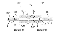
- FIG. 14A shows the format of each field set in the track portion Ta of one area of the sample storage disk 100a according to the second embodiment.
- a signal is recorded only on the track portion Ta (Ta12 to Ta15) made of the groove 111, and the signal is recorded on the track portion Ta (Ta11) made of the land 112. Is not recorded.
- the format of the signal recorded on the track portion Ta (Ta11) made of the groove 111 is the same as the format of the sample storage disk 100 in the first embodiment shown in FIG. 5A.
- the reason why the signal is not recorded in the track portion Ta (Ta11) including the land 112 is as follows. That is, when a signal is recorded on the track portion Ta composed of the lands 112, when the signal is read by scanning the track portion Ta composed of the grooves 111 with the beam spot B1, the track portion Ta composed of the land 112 adjacent thereto is simultaneously read. The beam spot B1 is applied, and light is modulated by the track portion Ta made of the land 112. For this reason, the reproduction RF signal RF from the track portion Ta composed of the groove 111 to be originally read is disturbed, and the signal cannot be acquired properly. For this reason, in the sample storage disk 100a according to the second embodiment, a signal is recorded only on the track portion Ta made of the groove 111.
- the fields F1, F4, F6, and F9 are Each is aligned in the disk radial direction Dr.
- the same signal is recorded in each of the track portions Ta (Ta12 and Ta13) including the grooves 111 arranged in the disk radial direction Dr.
- the portions on both sides of the beam spot B1 in the disc radial direction Dr become adjacent two track portions Ta (Ta12, Ta13). Therefore, the signals are modulated by signals recorded in the fields F1, F4, F6, and F9 of the track portion Ta (Ta12, Ta13). Therefore, even when the track portion Ta (Ta11) made of the lands 112 is scanned with laser light, the track portion Ta (Ta12, Ta13) adjacent to the track portion Ta (Ta11) in the disk radial direction Dr. The signals recorded in the fields F1, F4, F6, and F9 can be properly read.
- the signals V3 and Vs are appropriately transmitted from the track portions Ta (Ta12 and Ta13) adjacent to the disk radial direction Dr. To be acquired. Therefore, even when the track portion Ta (Ta11) made of the land 112 is scanned with the laser beam, the control shown in FIGS. 10B and 11A is performed when the track portion Ta (Ta12 to Ta15) made of the groove 111 is scanned with the laser beam. Can be done as well.
- signals recorded in the fields F3 and F8 shown in FIG. 14A that is, address signals
- the track portion Ta (Ta11) formed of the lands 112 is scanned with laser light
- the address signal cannot be properly acquired from F3 and F8.
- the track portion Ta (Ta11) including the land 112 is adjacent to the track portion Ta (Ta14) adjacent to the upstream side in the scanning direction Ds with respect to the track portion Ta (Ta11).
- Address signals acquired from the footer areas FT1 and FT2 and addresses acquired from the header areas HE1 and HE2 of the track part Ta (Ta15) adjacent downstream in the scanning direction Ds with respect to the track part Ta (Ta11). Based on the signal, the processing of FIG. 11B is performed.
- step S41 an address signal is acquired from the header areas HE1 and HE2 of the track portion Ta (Ta15) on the downstream side of the track portion Ta (Ta11) including the land 112.
- step S42 the track portion including the land 112 is obtained.
- Address signals are acquired from the footer areas FT1 and FT2 of the track portion Ta (Ta14) on the upstream side of Ta (Ta11).
- step S43 it is determined whether or not the relationship between both address signals is appropriate. That is, when the zone numbers of both address signals match, the track numbers of both address signals match, and the area numbers of both address signals have continuity, it is determined that the relationship between both address signals is appropriate.
- the area numbers of both address signals have continuity means that the area number acquired from the address signal recorded in the track portion Ta15 and the area number acquired from the address signal recorded in the track portion Ta14 are three consecutive numbers. This means that the area number relationship of the areas at both ends of the area is satisfied. For example, when the track portion Ta14, the track portion Ta11, and the track portion Ta15 are respectively arranged in areas with consecutive area numbers increased by 1 in this order, the address signal recorded in the track portion Ta11. When the difference between the area number acquired from the above and the area number acquired from the address signal recorded in the track portion Ta15 is 2, the area numbers of both address signals have continuity.
- the relationship between both address signals is not appropriate Determined.
- the processing of steps S44 and S45 is performed.
- the fluorescence signal is validated and the processing shown in FIG. 11B is performed. Finish.
- the region of the beam spot B1 modulated by the groove 111 is the beam spot B1.
- Dr the polarity of the tracking error signal TE is reversed every time the position where the beam spot B1 scans passes the boundary between the groove 111 and the land 112.
- FIG. 14B is a diagram illustrating a polarity inversion unit 51 that inverts the polarity of the tracking error signal TE according to the second embodiment.
- FIG. 14C is a diagram schematically illustrating the timing of reversing the scanning of the beam spot B1 and the polarity of the tracking error signal TE related to the sample storage disk 100a in the second embodiment.
- the polarity reversing unit 51 is provided in the servo circuit 50 shown in FIG.
- the signal detector 11 is provided in the signal processing circuit 10 shown in FIG.
- the polarity inversion unit 51 inverts the polarity of the tracking error signal TE and supplies it to the circuit unit for tracking servo.
- the beam spot B1 moves from the track portion Ta (Ta14) made of the groove 111 to the track portion Ta (Ta11) made of the land 112
- the track portion Ta (Ta14) and the track portion are moved.
- the polarity of the tracking error signal TE is inverted at the timing of passing through the boundary with Ta (Ta11).
- the beam spot B1 can be positioned on the track 102c without deviation even when the scanning position shifts from the groove 111 to the land 112.
- the beam spot B1 moves from the track portion Ta (Ta11) made of the land 112 to the track portion Ta (Ta15) made of the groove 111, the beam spot B1 passes through the boundary with the track portion Ta (Ta15) that becomes the track portion Ta (Ta11).
- the polarity of the tracking error signal TE returns to the original and is output from the polarity inverting unit 51 with the same polarity.
- the beam spot B1 can be positioned on the track 102c without deviation even when the scanning position shifts from the land 112 to the groove 111. Therefore, it is possible to stably extract the fluorescence signal.
- the same effect as that of the sample storage disk 100 in the first embodiment can be achieved.
- the area of the land 112 is also scanned with the laser light. Therefore, the number of areas scanned with the laser light is equal to the number of the areas that are scanned with the laser light.
- the scanning density for the sample container 101b is also doubled. Therefore, in the sample storage disk 100a in the second embodiment, the density at which the fluorescence signal is cut out is twice that of the sample storage disk 100 in the first embodiment, and a higher-definition fluorescent image is obtained.
- FIG. 14D schematically shows the structure of the groove 111, the land 112, and the pit 113 of another sample storage disk 100b according to the second embodiment. 14D, the same reference numerals are assigned to the same portions as those of the sample storage disk 100 according to Embodiment 1 shown in FIG. 2 showing the structure of the sample storage disk 100a.
- the land 102 may constitute the track 102c. That is, by forming the pit 113 on the land 112, the signal of each field shown in FIG. 5A may be recorded. In this case, the pit 113 is not formed in the groove 111 and extends monotonously and flatly.
- a signal is recorded on the track 102c in a pit row including a plurality of pits 113 formed on one of the groove 111 and the land 112.
- the light is not modulated by a different signal from a track adjacent to the track, and the signal can be read appropriately from the track.
- the track 102c is configured so that the groove 111 and the land 112 are switched each time the areas A0 to A8 are switched. For this reason, compared with the case where the track 102c is constituted by the series of grooves 111, the sample storage portion 101b can be scanned with a fine pitch in the disk radial direction Dr. In addition, a signal is recorded by the pit 113 only in the groove 111 of the groove 111 and the land 112. For this reason, when the groove 111 is scanned with the beam spot B1, the beam spot B1 is not modulated by a different signal of the adjacent land 112, and the signal can be appropriately read from the track 102c.
- the sample storage unit 101b is configured such that two boundaries in the disk circumferential direction Dc extend radially from the disk center Pc, respectively, when the sample storage disk 100a (100b) is rotated at a constant angular velocity, 1 Regardless of which track 102c that overlaps one sample storage unit 101b is scanned with laser light, the period during which the range of the sample storage unit 101b is scanned is substantially constant. Therefore, by extracting the fluorescence signal by the process of FIG. 11A of the first embodiment, a signal group of a series of fluorescence images along one track 102c can be acquired from the sample 100Sa accommodated in the sample accommodating portion 101b. it can. By connecting the acquired signal group in the disk circumferential direction Dc and the disk radial direction Dr, a fluorescence image of the entire sample storage unit 101b can be acquired.
- a signal En for recording that the track structure is switched from the groove 111 to the land 112 is recorded at the end EP of the groove 111 in the scanning direction Ds. Therefore, with the configuration of FIG. 14B, the track 102c can be smoothly scanned with the beam spot B1 by inverting the polarity of the tracking error signal TE in accordance with the detection of the signal En.
- the angle ranges of the areas A0 to A8 centered on the disc center Pc in the disc circumferential direction Dc are set to be equal to each other. Therefore, the fluorescence signal can be cut out from all the areas A0 to A8 by the same processing.
- the groove 111 includes a start signal V3 indicating the start of the sample storage unit 101b on the upstream side and the downstream side of the sample storage unit 101b in the scanning direction Ds, and the sample storage unit.
- An end signal Vs indicating the end of 101b is recorded.
- Each pit 113 for recording the start signal V3 included in the same area is formed to be aligned radially from the disc center Pc.
- Each pit for recording the end signal Vs included in the same area is formed so as to be aligned radially from the disc center Pc.
- the substrate 102 includes lands 112 that constitute the upper surface 102 p of the substrate 102, and grooves 111 that are provided on the upper surface 102 p and are connected to the lands 112.
- the track 102c is provided in the land 112 and the groove 111 so as to be alternately switched between the groove 111 and the land 112 at a plurality of boundaries.
- a signal is recorded on the track 102c in a pit row composed of a plurality of pits 113 formed on one of the groove 111 and the land 112.
- FIG. 15A shows the format of each field set in the track portion Ta (groove 111) of one area of the sample storage disk 100c in the third embodiment.
- FIG. 15B shows a part of the signal format of the sample storage disk 100c in the third embodiment, and particularly shows the field F5.
- FIG. 15C is a diagram schematically illustrating the configuration of the synchronization adjustment pit SB1 that constitutes the synchronization adjustment signal recorded on the sample storage disk 100c according to the third embodiment.
- 15A to 15C the same reference numerals are assigned to the same portions as those of the sample storage disk 100 in the first embodiment shown in FIGS. 1A to 6B.
- the pit 113 is not formed in the groove 111 of the field F5.
- the pit 113 for synchronization adjustment is formed in the groove 111 of the field F5.
- the fluorescence signal is sampled according to the sampling clock Sck having a constant period, and the signals SP1 to SPk are acquired.
- the sample storage disk 100 is rotated at a constant angular velocity for each zone as described above.
- the angular velocity of the rotation of the sample storage disk 100 fluctuates and uneven rotation occurs.
- the rotation unevenness may cause distortion in the scanning direction Ds in the signal of one column of each track, and as a result, the accuracy of the fluorescent image may decrease. .
- the pit 113 for synchronization adjustment is formed in the groove 111 of the field F5, and the distortion generated in the fluorescent image is corrected using the pit 113.
- synchronization adjustment pits SB1 to SB6 are arranged at a constant angular interval with respect to the disk center Pc.
- the synchronization adjustment pits SB1 are aligned in the disc radial direction Dr.
- the other synchronization adjustment pits SB2 to SB6 are similarly configured. That is, both ends of each pit 113 of the synchronization adjustment pits SB2 to SB6 are also aligned in the disk radial direction Dr in all zones and tracks.
- the field F5 overlaps the sample storage portion 101b in the entire length.
- both ends of the field F5 coincide with two boundaries (ends) arranged in the disk circumferential direction Dc of the sample storage unit 101b.
- No signal is recorded other than the synchronization adjustment pits SB1 to SB6 in the portion of the track portion Ta that overlaps the sample storage portion 101b, and the portion other than the portion where the synchronization adjustment pits SB1 to SB6 are recorded is a monotonically extending groove. Only 111 is formed.
- the synchronization adjustment pit SB1 includes a plurality of pits 113.
- five pits 113 are shown as the synchronization adjustment pits SB1, but actually, the synchronization adjustment pits SB1 are composed of about several tens of pits 113.
- the synchronization adjustment pit SB1 is formed of a combination of a pit length and a land length different from any other pit recorded in the groove 111.
- both ends of each pit 113 of the synchronization adjustment pit SB1 are aligned in the disc radial direction Dr in all zones and tracks.
- FIG. 15C shows the configuration of the synchronization adjustment pit SB1, but the synchronization adjustment pits SB2 to SB6 have the same contents and configuration as the synchronization adjustment pit SB1. That is, both ends of each pit 113 of the synchronization adjustment pits SB2 to SB6 are also aligned in the disk radial direction Dr in all zones and tracks.
- the beam spot B1 is the land 112 portion in the signal format of the second embodiment.
- both ends of the beam spot B1 are simultaneously applied to the pits 113 of the synchronization adjustment pits SB2 to SB6 formed in the groove 111 adjacent to the land 112 in the disk radial direction Dr. It can be detected properly. Therefore, even when the field F5 of the land 112 is scanned with the beam spot B1, the synchronization adjustment pits SB1 to SB6 can be properly detected.
- a signal output from the photodetector 210 is combined with a sampled signal in the same manner as a fluorescent image to obtain one signal light image, and from the acquired signal light image
- the synchronization adjustment pit SB1 can be detected by image processing.
- FIG. 16 is a configuration diagram of the fluorescence detection device 1a used together with the sample storage disk 100c.
- the fluorescence detection apparatus 1a illustrated in FIG. 16 further includes a cutout unit 15 and a superimposition unit 16, and an address signal is superimposed on a signal obtained by sampling the signal output from the photodetector 210 and output to the image processing unit 20.
- the image processing unit 20 connects the input signals to generate a signal light image corresponding to the fluorescent image.
- the image processing unit 20 processes the generated signal light image to detect the synchronization adjustment pits SB1 to SB6 of the track portion Ta on the signal light image.
- the image of one synchronization adjustment pit has a remarkably high correlation coefficient at a position aligned with the reference image of the synchronization adjustment pit. If the reference image is shifted in the scanning direction Ds, the correlation coefficient is adjusted to be remarkably low at any shift position.
- the synchronization adjustment pits SB1 to SB6 are formed of pit patterns that satisfy such a correlation with the reference image in detection by image processing.
- FIG. 17A schematically shows a detection position where the synchronization adjustment pits SB1 to SB6 are detected on the signal light image obtained from the sample storage disk 100c by a solid line.
- the shift amount between the track portions Ta of the synchronization adjustment pits SB1 to SB6 gradually increases as the signal proceeds from the cutout start position to the downstream side in the scanning direction Ds.
- the shift amounts of the synchronization adjustment pits SB1 to SB6 between the track portions Ta adjacent to each other in the disk radial direction Dr are relative to the position in the scanning direction Ds from the position where the cutting starts. Increases monotonically and increases linearly.
- the shift amount of each of the synchronization adjustment pits SB1 to SB6 between the track portions Ta periodically repeats the maximum value and the minimum value in 8 to 10 track portions, and the shift amount Remains within the range of 100 pixels.
- FIG. 17A schematically shows that the detection positions of the synchronization adjustment pits SB1 to SB6 change due to the rotation unevenness of the sample storage disk 100 for convenience of explanation.
- the shift amounts of the synchronization adjustment pits SB1 to SB6 between the track portions Ta adjacent to each other in the disk radial direction Dr are periodically set to the maximum value every 8 to 10 track portions. It fluctuates periodically to repeat the minimum value.
- the 16 corrects the fluorescent image based on the distribution of the synchronization adjustment pits SB1 to SB6 on the signal light image shown in FIG. 17A. Specifically, the image processing unit 20 corrects the fluorescence image so that the fluorescence signals cut out at the positions of the synchronization adjustment pits SB1 to SB6 on the fluorescence image are arranged in a line in the disk radial direction Dr. .
- FIG. 17B and FIG. 17C schematically show fluorescent image correction processing. Specifically, FIG. 17B shows a fluorescence image before correction by the signal light image, and FIG. 17C shows a fluorescence image after correction by the signal light image. For convenience, FIGS. 17B and 17C show the detection positions of the synchronization adjustment pits SB1 to SB6 by broken lines.
- the synchronization adjustment pit SB6 is located on the most downstream side in the scanning direction Ds.
- the image processing unit 20 uses, as a reference signal group, a signal group composed of signals of the track portion Ta of the track number Tx whose detection position of the synchronization adjustment pit SB6 is the most downstream in the scanning direction Ds among the track numbers T0 to Tm. Decide.
- a signal group (correction) composed of signals of the track portion Ta of other track numbers Ty (y is an arbitrary integer satisfying 0 ⁇ y ⁇ x ⁇ 1 or x + 1 ⁇ y ⁇ m) with reference to the reference signal group Interpolation processing is applied to the signal group).
- the image processing unit 20 scans in the scanning direction Ds between the signal at the detection position of the synchronization adjustment pit SB6 in the reference signal group and the signal at the detection position of the synchronization adjustment pit SB6 in the correction signal group. The amount of deviation ds is obtained. Thereafter, the image processing unit 20 evenly distributes the gaps of the interpolation signals whose number of deviations ds is zero to a range from the correction signal group cutting start position to the detection position of the synchronization adjustment pit SB6 at regular intervals.
- the image processing unit 20 also performs the process of distributing the gaps of the interpolation signals at regular intervals also in the range after the synchronization adjustment pit SB6 of the correction signal group, and performs all processing up to the cut-out end position of the correction signal group.
- the gap of the interpolation signal is distributed to the range based on the shift amount ds.
- the image processing unit 20 adds an interpolation signal based on signals before and after the gap (for example, an average value of the signals before and after) to the distributed gap.
- the image processing unit 20 acquires the fluorescence image after the interpolation processing shown in FIG. 17C from the fluorescence image before correction shown in FIG. 17B. Since a new signal is inserted into the signal group of each track by the interpolation process, as shown in FIG. 17C, the period of the signal group of each track part is longer than before correction.
- the image processing unit 20 extracts only the fluorescence signal in the range of the extraction period Tsp similar to the fluorescence image before the correction from the fluorescence image after the interpolation process, and acquires the image based on the extracted fluorescence signal as the corrected fluorescence image. .
- the amount of deviation between the reference signal group and the correction signal group is obtained using the synchronization adjustment pit SB6 among the synchronization adjustment pits SB1 to SB6.
- the shift amount ds between the reference signal group and the correction signal group may be obtained using any one of the synchronization adjustment pits SB1 to SB5 other than the synchronization adjustment pit SB6.
- the shift amount between the adjacent track portions in the scanning direction Ds increases linearly with respect to the distance from the cutout start position of the position in accordance with the change in the position in the scanning direction Ds.
- the six synchronization adjustment pits SB1 to SB6 are not necessarily arranged in the field F5 as shown in FIG. 15B.
- any one of the synchronization adjustment pits SB1 to SB6 may be arranged in the field F5.
- the signal group cannot be corrected for the track.
- FIG. 15B by arranging a plurality of synchronization adjustment pits SB1 to SB6 in the field F5, the probability that at least any synchronization adjustment pit can be detected from one track is increased.
- the distribution of the synchronization adjustment pits SB1 to SB6 shown in FIG. 17A is previously compared with the reference image of the synchronization adjustment pits SB1 to SB6 and the signal light image. Is acquired.
- the detection method of the synchronization adjustment pits SB1 to SB6 is not limited to this, and synchronization is performed based on the correlation between the signal waveform acquired from one track and the signal waveform acquired from a track adjacent to this track. Adjustment pits SB1 to SB6 may be detected.
- the scanning direction Ds is centered on the timing at which the signal waveform is acquired for a track portion adjacent to this track.
- a predetermined range for example, a range of about 100 pixels
- a correlation coefficient between this signal waveform and the adjacent track portion signal is obtained.
- the position where the obtained correlation coefficient is remarkably high is specified as the position of the synchronization adjustment pit in the adjacent track portion.
- the difference between the position specified as the adjacent track and the position at which the signal waveform is acquired in the track is acquired as the shift amount of the synchronization adjustment pits in these two tracks.
- the positions of the synchronization adjustment pits SB1 to SB6 are not necessarily detected by image processing of the signal light image as described above.
- the synchronization adjustment pits SB1 are obtained from the reproduction RF signal RF.
- the synchronization adjustment pits SB1 to SB6 may be detected depending on whether or not a waveform (bit signal) corresponding to SB6 is obtained.
- the fluorescent image correction processing is not limited to the interpolation processing as described above, and other processing may be used. For example, only a part of the field F5 in the disk circumferential direction Dc may be cut out, and only the position in the scanning direction Ds may be corrected using the shift amount.
- the image is divided every 1000 pixels in the disk circumferential direction Dc to obtain a plurality of divided images, and the shift amount at the center (500th pixel) of these divided images is determined from the distance from the synchronization adjustment pit at the center. May be obtained by linear interpolation based on this, and adjustment may be performed by moving the pixel in the scanning direction Ds for each track portion based on this value.
- the signal group acquired in the period for scanning the field F5 is left without being deleted except for the signal group near the scanning end position. Therefore, for example, it is possible to prevent the fluorescence signal cut out at the timing when the laser light scans the red blood cells RC infected with malaria from being deleted. Therefore, target cells such as malaria can be detected more appropriately.
- FIG. 18 shows a part of the signal format of another sample storage disk 100d according to the third embodiment.
- the same reference numerals are assigned to the same parts as those of the sample storage disk 100c shown in FIG. 15A.
- a signal for synchronization adjustment is recorded by the synchronization adjustment bits SB1 to SB6 in the field F5 of the sample storage disk 100 in the first embodiment shown in FIG. 5A.
- signals for synchronization adjustment are recorded by the synchronization adjustment bits SB1 to SB6 in the field F5 of the sample storage disk 100a in the second embodiment shown in FIGS. 13 and 14A.
- the sample storage disk 100d can more smoothly suppress the distortion of the fluorescent image due to the rotation unevenness of the sample storage disk 100d by the synchronization adjustment bits SB1 to SB6, and, similarly to the sample storage disk 100a in the second embodiment, 2 A double-density high-definition fluorescent image can be obtained.
- a signal for synchronization adjustment is recorded by forming pits 113 in the groove 111.
- a signal for synchronization adjustment is recorded by forming pits 113 in the groove 111.
- the track areas 102a of the sample storage discs 100 and 100a to 100c in the first to third embodiments are divided into nine areas A0 to A8 in the disc circumferential direction Dc.
- the number of areas in which the area of the sample storage disk 100 is divided in the disk circumferential direction Dc is not limited to this.
- the track area 102a of the sample storage disk 100b is an odd number. Divide into areas. In this case, a fluorescent image can be acquired for a plurality of types of samples 100Sa by setting the number of areas allocated to the sample storage disk 100 to an odd number of 3 or more.
- the shape of the sample container 101b and the internal structure of the sample container 101b can be changed as appropriate other than the forms shown in FIGS. 1A and 1B. Furthermore, it is also possible to delete or change a predetermined field as appropriate from the signal format set in one track portion Ta and the format of FIG. 5A, or to add a new field.
- both ends of the field F5 do not have to coincide with two boundaries (ends) aligned in the disk circumferential direction Dc of the sample storage unit 101b of the sample storage disks 100, 100a, 100b, and 100c in the first to third embodiments.
- the both ends of the field F5 may be set so that the range of the field F5 is slightly wider than the range between the two boundaries (ends) of the sample storage unit 101b. Further, the content of the signal recorded in each field can be appropriately changed from the signal shown in FIG. 6A.
- the shape of the sample container 101b as viewed from above is not necessarily a trapezoid.
- the shape of the sample storage portion 101b viewed from above may be, for example, a U-shape that extends in the outer peripheral direction from the inner peripheral position, then bends in the disk peripheral direction Dc, and then extends in the inner peripheral direction.
- the range of the field F5 shown in FIG. 5A can include a portion that does not overlap the sample storage portion 101b.
- the synchronization adjustment pits of the third embodiment may be arranged in a portion of the field F5 that does not overlap the sample storage unit 101b.
- the signal of each field does not necessarily have to be recorded in the groove 111, and the signal of each field may be recorded in the land 112 instead of the groove 111. Further, all or part of the signals in the fields F1 to F9 may be recorded by wobble instead of the pits 113.
- the configuration of the fluorescence detection pickup 200 can be appropriately changed from the configuration of FIG.
- the sample storage disk in the fourth embodiment has basically the same structure as the sample storage disks 100, 100a to 100d in the first to third embodiments, but the structures of the fields F2, F5, and F7 are different.
- a synchronization signal is recorded in a pit row including one or more pits in a portion of the track portion Ta that overlaps the sample storage portion 101b.
- a predetermined modulation structure is formed in the track portion Ta on the upstream side of the address signal. This modulation structure is also formed by a pit string composed of one or more pits, like the address signal.
- FIG. 19 shows the formats of the fields F1 to F9 set in the plurality of track portions Ta (grooves 111) in the respective areas Ax of the areas A0 to A8 of the sample storage disk 100e in the fourth embodiment.
- the above-described modulation structure Md is formed in the fields F2 and F7, and the synchronization signal Sy is recorded in the field F5.
- the field F5 overlaps with the sample storage portion 101b in the entire length. That is, both ends of the field F5 coincide with two boundaries (ends) arranged in the disk circumferential direction Dc of the sample storage unit 101b. Therefore, the synchronization signal Sy is recorded in the portion of the track portion Ta that overlaps the sample storage portion 101b.
- a modulation structure Md is formed by the pits 113 shown in FIG.
- the fields F2 and F7 are also aligned in the disk radial direction Dr in all track portions Ta in the same zone and the same area.
- FIG. 20 shows a signal format of fields F1 to F9 of a certain track portion Ta1 among the plurality of track portions Ta.
- the same reference numerals are assigned to the same parts as those of the sample storage disk 100 shown in FIG. 6A.
- Each of the plurality of track portions Ta has the same configuration as the track portion Ta1.
- a hatched portion indicates a region where the pit 113 is formed in the groove 111, and a white portion where the pit 113 is not formed is a white portion where the pit 113 is not formed (see FIG. 2). ) Only the groove 111 is shown.
- the time length of the space 113s used for signal recording is set to eight stages of time lengths 1T to 8T, and the time length of the pit 113 used for signal recording is also set to time lengths 1T to 8T. There are 8 levels.
- the time length of the space 113s and the pit 113 of the modulation structure Md is set to a time length other than 1T to 8T. That is, the modulation structure Md is for modulating the reflected light reflected by the semi-transmissive film 102d, and a predetermined signal is not recorded by the pits 113 and the spaces 113s in the modulation structure Md. The signal is not reproduced from there.
- the signal En is recorded in the fields F1 and F9 as in the case of the sample storage disc 100 in the first embodiment.
- the signal En recorded in the field F1 indicates the start end SP (see FIG. 19) of the track portion Ta of the area Ax
- the signal En recorded in the field F9 indicates the end EP (see FIG. 19) of the track portion Ta of the area Ax. ).
- a signal having the same pattern as the signal En that is, a synchronization signal Sy composed of alternately repeated pits having a time length 2T and spaces having a time length 2T is recorded.
- the synchronization signal Sy is used for rotation control of the sample storage disk 100 and adjustment of the fluorescence signal cut-out timing.
- the signal En recorded in the fields F1 and F9 is also used for the rotation control of the sample storage disk 100 and the adjustment of the fluorescence signal cut-out timing, like the synchronization signal Sy.
- a pit having a time length 10T that is 10 times the time length 1T and a time that is 10 times the time length 1T are alternately repeated.
- a modulation structure Md comprising a space having a length of 10T is formed over the entire length of the field.
- a start signal V3 indicating the position where the sample storage unit 101b starts in the scanning direction Ds is recorded in the field F4. Yes.
- an end signal Vs indicating the end position of the sample storage unit 101b in the scanning direction Ds is recorded in the field F6. Yes.
- the field F3 includes three header areas HE0 to HE2.
- the field F8 is composed of three footer areas FT0 to FT2, as with the sample storage disk 100 in the first embodiment.
- the pits and spaces formed in the fields other than the fields F3 and F8 have a disk diameter in all track portions Ta in the same zone and the same area. It is aligned in the direction Dr.
- the pits and spaces formed in the fields F1 and F9 are aligned in the disk radial direction Dr in the track portions Ta included in all the zones of the same area. ing.
- pits and spaces each having a time length of 10T formed in the field F5 are aligned in the disc radial direction Dr in the track portions Ta included in all zones of the same area. Since the pits and spaces formed in the fields F3 and F8 vary in length depending on the contents of the address signal, the positions in the disk circumferential direction Dc are shifted between the track portions Ta.
- the fluorescence detection device in the fourth embodiment includes a fluorescence detection pickup 200 shown in FIG.
- FIG. 21 is a configuration diagram of the signal arithmetic circuit 300 and the output processing circuit 400 in the fourth embodiment.
- FIG. 22 is a configuration diagram of the fluorescence detection apparatus 1b according to the fourth embodiment. 21 and 22, the same reference numerals are assigned to the same portions as those in the fluorescence detection device 1 in the first embodiment shown in FIGS. 8 and 9.
- the output processing circuit 400 amplifies the analog signal generated by the signal arithmetic circuit 300 and the fluorescence signal that is the analog signal output from the fluorescence detector 211, converts the analog signal into a digital signal, and outputs the digital signal.
- the signal calculation circuit 300 and the output processing circuit 400 are arranged on the substrate of the fluorescence detection pickup 200.
- the focus error signal FE, the tracking error signal TE, and the reproduction RF signal RF which are analog signals generated by the signal arithmetic circuit 300, are amplified by the output processing circuit 400 and converted into a digital signal, and then the focus error signal FEd, The tracking error signal TEd and the reproduction RF signal RFd are output to the signal processing circuit 10 and the servo circuit 50 (see FIG. 22).
- the signal FL which is an analog signal output from the fluorescence detector 211, is amplified by the output processing circuit 400 and AD-converted into a digital signal, and then output as a signal FLd to the signal processing circuit 10 (see FIG. 22).
- the signal processing circuit 10 of the fluorescence detection device 1b processes the fluorescence signal FLd and the reproduction RF signal RFd output from the fluorescence detection pickup 200.
- the fluorescence signal FLd is obtained by amplifying the signal FL output from the fluorescence detector 211 (see FIG. 7) by the output processing circuit 400 of FIG. 21, and the reproduction RF signal RFd is the adder of FIG.
- the reproduction RF signal RF output from 307 is amplified by the output processing circuit 400 and obtained.
- the signal processing circuit 10 includes a signal detection unit 11, a signal reproduction unit 12, a cutout unit 13, and a superposition unit 14.
- the signal detection unit 11 and the signal reproduction unit 12 constitute a signal acquisition unit 11a.
- the signal detection unit 11 processes the reproduction RF signal RFd input from the fluorescence detection pickup 200, detects various signals shown in FIG. 20, and sends the detected signals to the signal reproduction unit 12, the cutout unit 13, and the controller 40. Output.
- the signal reproduction unit 12 reproduces the signals in the fields F3 and F8 input from the signal detection unit 11, that is, the signals in the header areas HE0 to HE2 and the footer areas FT0 to FT2, and acquires an address signal.
- the signal reproducing unit 12 outputs the acquired address signal to the superimposing unit 14.
- the cutout unit 13 outputs each sample value obtained by sampling the fluorescence signal FLd input from the fluorescence detection pickup 200 with the sampling clock Sck having a predetermined cycle to the superposition unit 14.
- the cutout unit 13 starts sampling of the fluorescent signal FLd in response to the start signal V3 (see FIG. 19) detected by the signal detection unit 11, and the end signal Vs (see FIG. 19) is detected by the signal detection unit 11. In response to this, the sampling of the fluorescence signal FLd is terminated.
- the extraction unit 13 samples the fluorescence signal FLd output from the fluorescence detection pickup 200 so that the signal is extracted from the sample 100Sa at regular intervals based on the synchronization signal Sy input from the signal detection unit 11.
- the interval that is, the period of the sampling clock Sck is adjusted. That is, the cutout unit 13 generates the sampling clock Sck synchronized with the signal En and the synchronization signal Sy input from the signal detection unit 11, and samples the fluorescent signal FLd according to the generated sampling clock Sck.
- the sample storage disk 100e is rotated at a different angular velocity for each zone. Accordingly, the time during which the track portion Ta is scanned with the laser light varies from zone to zone. For this reason, when a fluorescence signal is cut out with a timing signal having the same period for each zone, the number of cut out signal groups differs for each zone.
- the sampling clock Sck in the cutout unit 13 is adjusted so that the same number of signal groups are cut out from the track portion Ta of each zone. Specifically, as described above, the cutout unit 13 generates the sampling clock Sck synchronized with the signal En and the synchronization signal Sy input from the signal detection unit 11. For this reason, the fluorescence signal FLd is cut out at substantially the same angular interval in each zone.
- the superimposing unit 14 adds the address signal input from the signal reproducing unit 12 to the fluorescence signal acquired by the clipping unit 13 and outputs the signal to the image processing unit 20.
- the image processing unit 20 connects the input signal groups and generates a fluorescence image for each of the areas A0 to A8.
- the image processing unit 20 performs image processing on the fluorescence image, counts the number of fluorescent bright spots, and calculates the infection rate of malaria in the red blood cells RC. These fluorescent images, count values, infection rates, and the like are output from the image processing unit 20 to the input / output unit 30 as needed.
- the controller 40 controls the servo circuit 50 and the signal processing circuit 10 so that the period from the start signal V3 in which the address signal has changed to the end signal Vs is scanned again with the laser light and the fluorescent signal is extracted.
- the servo circuit 50 controls the objective lens actuator 207 based on the focus error signal FEd and the tracking error signal TEd input from the fluorescence detection pickup 200 via the output processing circuit 400.
- the servo circuit 50 controls the spindle motor 220 so that the zones Z0 to Zn shown in FIG. 3B are scanned by the beam spot B1 at the angular velocity set in each zone.
- the servo circuit 50 controls the spindle motor 220 so as to suppress the rotation unevenness of the sample storage disk 100e based on the signal En and the synchronization signal Sy input from the signal detection unit 11. That is, the servo circuit 50 controls the spindle motor 220 so as to eliminate the phase shift between the signal En and the synchronization signal Sy input from the signal detection unit 11 and the reference clock.
- the servo circuit 50 is a thread for sending the fluorescence detection pickup 200 in the disk radial direction Dr of the sample storage disk 100e so that the beam spot B1 can be scanned from the outermost position to the innermost position of the track 102c.
- the motor 240 is controlled.
- FIG. 23A is a configuration diagram of an output processing circuit 900 according to a comparative example provided instead of the output processing circuit 400 shown in FIG.
- FIG. 23B schematically shows the reproduction RF signal RF input to the AD conversion circuit 402 of the output processing circuit 900 according to the comparative example.
- FIG. 23B showing a comparative example schematically shows the waveform of the voltage of the reproduction RF signal RF when the modulation structure Md is not formed in the fields F2 and F7.
- FIG. 23B also shows a portion of a period corresponding to the fields F2 to F8 of the reproduction RF signal RF.
- the output processing circuit 900 of the comparative example includes an amplifier 401 and an AD conversion circuit 402 as a circuit unit for processing the reproduction RF signal.
- the amplifier 401 amplifies the reproduction RF signal RF
- the AD conversion circuit 402 converts the amplified reproduction RF signal RF into a reproduction RF signal RFd that is a digital signal.
- the reproduction RF signal RF is shaken by signals (pits and spaces) recorded in the fields F3 to F6 and F8.
- the voltage of the reproduction RF signal RF varies from the baseline voltage V1 to the peak voltage V1p.
- the baseline voltage V2 in the scanning period corresponding to the field other than the field F5 the voltage of the reproduction RF signal RF varies from the baseline voltage V2 to the peak voltage V2p.
- the peak voltage V1p is equal to the baseline voltage V2, but may be different.
- the reflectance differs between the region that overlaps the sample container 101b and the region that does not overlap, so that the baseline voltage V1 in the scanning period corresponding to the field F5 and the scanning period corresponding to the field other than the field F5.
- the voltage range of AD conversion is set so as to include the amplitude range Vd of the voltage waveform that fluctuates in the baseline voltages V1 and V2.
- the baseline voltage of a reflected light signal obtained when a track is scanned with laser light changes due to warpage or individual variation. Also, the baseline voltage changes between a portion that overlaps the flow path of the track and a portion that does not overlap the flow path.
- an analog voltage waveform of a reflected light signal obtained by scanning the track with a laser beam is converted into a digital signal by an AD converter. At this time, since the voltage range and resolution of the AD converter are limited, if the baseline voltage of the voltage waveform varies, the decoding accuracy of the signal decreases.
- FIG. 24A is a configuration diagram of the output processing circuit 400 according to the fourth embodiment.
- FIG. 24B schematically shows a reproduction RF signal RF input to the AD conversion circuit 402 of the output processing circuit 400 according to the fourth embodiment when the modulation structure Md is not formed in the groove 111 of the sample storage disk.
- the vertical axis represents the voltage of the reproduction RF signal RF
- the horizontal axis represents time.
- a filter 403 is disposed in front of the amplifier 401, and a switch 404 is provided in the subsequent stage of the AD conversion circuit 402.
- the filter 403 passes a high frequency component that is a frequency component higher than a certain frequency in the entire frequency band of the reproduction RF signal RF, and has a frequency equal to or lower than the certain frequency in the entire frequency band of the reproduction RF signal RF.
- This is a high-pass filter that blocks low-frequency components that are components without passing them.
- the high-frequency component of the reproduction RF signal RF is a frequency component that fluctuates due to pits and spaces.
- the filter 403 By arranging the filter 403 in front of the amplifier 401, the high frequency component of the reproduction RF signal RF is extracted as shown in FIG. 24B. At this time, the filter 403 functions to bring the amplitude center of the voltage waveform in the period corresponding to the field F5 closer to the amplitude center of the voltage waveform in the period corresponding to the field other than the field F5. Thereby, the amplitude range Vd of the voltage waveform is compressed, and the reproduction RF signal RF can be AD-converted with high resolution without greatly expanding the voltage range of the AD conversion circuit 402.
- the reproduction RF signal RF when the reproduction RF signal RF is passed through the filter 403, the reproduction RF signal is output during a period from when the baseline voltage is switched until the amplitude center of the voltage waveform converges to a predetermined level. Transient distortion may occur in the RF voltage waveform.
- transient distortion occurs in the voltage waveform when the baseline voltage is switched to the baseline voltage V1, that is, when scanning is shifted from the field F4 to the field F5.
- the baseline voltage is switched to the baseline voltage V2, that is, when the scanning shifts from the field F4 to the field F5
- a transient distortion occurs in the voltage waveform.
- the baseline voltage V2 also changes due to the warp of the sample storage disk 100 and the variation of the individual, and this also causes a transition to the reproduced RF signal RF, such as the waveform of the field F2 in FIG. 24B. Distortion may occur.
- the reproduction RF signal RF maintains the peak voltage V2p in the period corresponding to the fields F2 and F5. Since it is not shaken, in these periods, the function of making the amplitude center of the reproduction RF signal RF close to the amplitude center of the reproduction RF signal in the period up to these periods becomes difficult to work.
- the distortion generated in the reproduction RF signal RF does not sufficiently converge in the period corresponding to the fields F2 and F7, and the distortion easily shifts to the fields F3 and F8.
- the waveform distortion reaches the voltage waveforms of the fields F3 and F8, that is, the voltage waveform corresponding to the address signal. For this reason, the address signal may not be decoded properly.
- the modulation structures Md are formed in the fields F2 and F7.
- FIG. 24C schematically illustrates the reproduction RF signal RF input to the AD conversion circuit 402 of the output processing circuit 400 when the sample storage disk 100e in which the modulation structure Md is formed in the groove is scanned according to the fourth embodiment. Show.
- the vertical axis represents the voltage of the reproduction RF signal RF
- the horizontal axis represents time.
- the modulation structures Md are formed in the fields F2 and F7 upstream of the fields F3 and F8 where address signals are recorded in the scanning direction Ds. Therefore, as shown in FIG. 24C, the reproduction RF signal RF is modulated and shaken by the modulation structure Md even in the period corresponding to the fields F2 and F7. Therefore, the distortion generated in the reproduction RF signal RF due to the fluctuation of the baseline voltage of the reproduction RF signal RF corresponds to the fields F2 and F7 by the filter 403 before reaching the reproduction RF signal RF in the period corresponding to the fields F3 and F8. It is converged in the period to do. Therefore, the voltage waveforms of the fields F3 and F8, that is, the voltage waveform corresponding to the address signal are not easily distorted, and therefore the address signal can be properly decoded.
- the amplitude of the voltage waveform in the period corresponding to the field F5 is different from the amplitude of the voltage waveform in the period other than the period corresponding to the field F5. This is due to the fact that the reflectance differs between the region of the track portion Ta that overlaps the sample storage portion 101b and the region that does not overlap the sample storage portion 101b. In order to improve the S / N ratio with noise, it is preferable to align the voltage waveform having the smaller amplitude with the amplitude of the voltage waveform having the larger amplitude.
- FIG. 25A is a configuration diagram of another output processing circuit 400a according to the fourth embodiment. 25A, the same reference numerals are given to the same portions as those of the output processing circuit 400 shown in FIG. 23A.
- the output processing circuit 400a constitutes an AGC (Automatic Gain Control) circuit 1400a, and a voltage waveform having a smaller amplitude can be aligned with the amplitude of a voltage waveform having a larger amplitude.
- AGC Automatic Gain Control
- the reproduction RF signal RF is detected by the signal processing circuit 10, an average value (DC component) of the preceding reproduction RF signal RF is obtained, and the obtained average value is converted into a D / A conversion circuit.
- the AGC circuit 1400a is configured by sequentially converting to an analog signal in 405, amplifying the analog signal by the amplifier 406, and returning the analog signal to the amplifier 401.
- the gain of the amplifier 401 is changed by the analog signal, and a voltage waveform having a smaller amplitude can be aligned with the amplitude of the voltage waveform having a larger amplitude and input to the AD conversion circuit 402.
- FIG. 25B is a configuration diagram of still another output processing circuit 400b according to the fourth embodiment. 25B, the same reference numerals are assigned to the same portions as those of the output processing circuits 400 and 400a shown in FIGS. 23A and 25A.
- the output processing circuit 400b constitutes an AGC circuit 1400b, and a voltage waveform having a smaller amplitude can be aligned with the amplitude of a voltage waveform having a larger amplitude.
- the reproduced RF signal RF is detected by the detection circuit 407, the DC component of the preceding reproduced RF signal is obtained, the obtained DC component is amplified by the amplifier 408, and returned to the amplifier 401.
- an AGC circuit 1400b is configured.
- the gain of the amplifier 401 is changed by the analog signal, and a voltage waveform having a smaller amplitude can be aligned with the amplitude of the voltage waveform having a larger amplitude and input to the AD conversion circuit 402.
- a relatively large distortion occurs in the reproduction RF signal RF in the period F5a immediately after the start of the period corresponding to the field F5. For this reason, in the period F5a, it may be difficult to properly decode the synchronization signal Sy from the reproduction RF signal RF.
- the unstable synchronization signal Sy acquired from the reproduction RF signal RF in the period F5a is used for the synchronization control of the spindle motor 220 in the servo circuit 50 and the generation of the timing signal in the cutout unit 13, the accuracy of the synchronization control can be improved. There is a possibility that the accuracy of the generation of the timing signal is lowered.
- the controller 40 shown in FIG. 22 supplies the control signal Scon to the switch 404 shown in FIG. 24A, FIG. 25A, or FIG. 25B in the period F5a.
- the switch 404 receives the control signal Scon
- the switch 404 does not supply the signal processing circuit 10 with the reproduction RF signal RFd converted into a digital signal by AD.
- the switch 404 supplies the signal processing circuit 10 with the reproduction RF signal RFd converted into a digital signal.
- the supply of the reproduction RF signal to the signal processing circuit 10 is interrupted in the period F5a, and the synchronization control and the generation of the timing signal using the unstable synchronization signal Sy are suppressed.
- the reproduction RF signal RFd is not supplied to the signal processing circuit 10 in the period F5a, the synchronization signal Sy may not be recorded in the range of the field F5 corresponding to the period F5a.
- FIG. 25C shows the format of the track area 102a of another sample storage disk 100f according to Embodiment 4, and particularly shows the vicinity of the boundary between the fields F4 and F5.
- a modulation structure Md is formed in the range of the field F5 corresponding to the period F5a instead of the synchronization signal Sy.
- the synchronization signal Sy can be converged in the period F5a by the filter 403 in the same manner as the address signal. For this reason, the synchronization signal Sy can be obtained appropriately.
- the configuration of the circuit unit that processes the reproduction RF signal RF among the circuit units included in the output processing circuit 400 has been described, but is included in the output processing circuit 400.
- the circuit unit that processes the focus error signal FE, the tracking error signal TE, and the fluorescence signal FL may also be configured in the same manner as in FIG. 24A or 25A and 25B.
- an address signal is acquired by the same processing as that in the first embodiment shown in FIG. 10A, FIG. 10B, FIG. 11A, and FIG.
- tracking control, fluorescence signal extraction, and extraction signal invalidation processing are performed.
- FIG. 26A is a flowchart showing processing for stopping the output of various signals from the output processing circuit 400.
- FIG. 26B shows a table referred to in setting the mask period.
- the controller 40 Based on the address signal obtained from one of the header areas HE1 and HE2 of the field F3 of the track portion Ta1 among the plurality of track portions Ta, the controller 40 addresses the track portion Ta1 (zone number, area number, When the track number is acquired (S51: YES), a mask period corresponding to the address is set with reference to the table shown in FIG. 26B (S52). When the controller 40 does not obtain an address signal (S51: No), the controller 40 determines again whether or not the address signal has been acquired in step S51.
- the sample storage disk 100e is driven at a constant angular velocity in the zone. Therefore, the linear velocity is closer between the inner circumference side closer to the disk center Pc and the outer circumference side farther from the disk center Pc. Differently, the frequency of the reproduction RF signal RF is different. For this reason, the period F5a shown in FIG. 24C differs between the inner peripheral side and the outer peripheral side of the zone. Further, since the angular velocities are different in the zones Z0 to Zn, the period F5a shown in FIG. 24C is different in the track portion Ta having the same track number in different zones.
- the controller 40 sets a period F5a corresponding to the acquired address as a mask period (S52).
- the controller 40 stops outputting various signals from the output processing circuit 400 during the mask period.
- the controller 40 holds a table shown in FIG. 26B in advance. This table stores addresses Ad1, Ad2,..., Adx of the track portion Ta and mask periods Mt1, Mt2,..., Mtx which are periods F5a corresponding to the addresses Ad1, Ad2,. From this table, the controller 40 sets a mask period corresponding to the address of the track portion Ta being scanned in step S52. Note that the table in FIG. 26B may be prepared for each zone or for each area.
- the controller 40 monitors whether or not the start signal V3 is detected from the field F4 located immediately before the field F5 in the scanning direction Ds (S53).
- the controller 40 gives the control signal Scon to the switch 404 shown in FIG. 24A or FIG. 25A and FIG. 25B.
- the output processing circuit 400 cuts off the signal supply to the signal processing circuit 10 (S54).
- the controller 40 continues to supply the control signal Scon to the switch 404 until the mask period set in step S52 ends (S55). When the mask period ends (S55: YES), the controller 40 ends the supply of the control signal Scon. Thereby, supply of the signal from the output processing circuit 400 to the signal processing circuit 10 is resumed (S56). Thereafter, the controller 40 returns the process to step S51 and repeats the same process.
- the fluorescence detection device 1b according to the fourth embodiment performs a fluorescence signal cut-out process by the process shown in FIG. 12, as with the fluorescence detection device 1 according to the first embodiment.
- the AGC circuits 1400a and 1400b shown in FIGS. 25A and 25B can improve the S / N ratio by aligning the amplitude of the voltage after passing through the filter 403 to the larger amplitude. As a result, signal processing can be performed with high accuracy by the circuit unit at the subsequent stage, and a highly accurate fluorescent image can be acquired.
- header regions HE1 and HE2 are set on the upstream side of the sample storage unit 101b in the scanning direction Ds in the track portion Ta straddling the sample storage unit 101b, and downstream of the sample storage unit 101b in the scanning direction Ds.
- Footer areas FT1 and FT2 are set on the side.
- the modulation structure Md is formed on the upstream side of the header regions HE1 and HE2, and the modulation structure Md is formed on the upstream side of the footer regions FT1 and FT2. Therefore, as described above, the address signal can be accurately detected from the upstream side and the downstream side of the sample storage unit 101b. Then, the processing shown in FIG.
- a synchronization signal (signal En, synchronization signal Sy) that modulates the light reflected from the track 102c monotonously, that is, modulates with a constant frequency and a constant amplitude. Recorded in the track portion Ta. Then, the rotation of the sample storage disk 100e is controlled to be synchronized with the signals En and Sy. Therefore, the rotation unevenness of the sample storage disk 100e can be suppressed, and as a result, the accuracy of the fluorescent image can be increased.
- the sampling clock Sck in the cutout unit 13 is generated so as to be synchronized with a signal for synchronization (signal En, synchronization signal Sy). Therefore, even if rotation unevenness occurs in the sample storage disk 100e, the cut-out portion 13 can cut out the fluorescence signal at a constant angular interval. Thereby, the precision of a fluorescence image can be improved.
- the synchronization signal Sy is recorded in the field F5 that overlaps the sample container 101b. Therefore, the synchronization signal Sy can be acquired while the sample storage unit 101b is scanned with the laser beam, and during this time, the rotation control of the sample storage disk 100e and the synchronization adjustment of the sampling clock Sck can be performed. Therefore, it is possible to more reliably suppress the occurrence of rotation unevenness in the sample storage disk 100e, particularly during the period in which the sample storage unit 101b is scanned, and to more reliably suppress the synchronization of the sampling clock Sck.
- the signal supply from the fluorescence detection pickup 200 to the signal processing circuit 10 is cut off, and the synchronization signal (synchronization signal Sy) is used. Control is stopped. Thereby, the synchronization control by the unstable signal for synchronization (synchronization signal Sy) is suppressed, and it can prevent that the precision of synchronization control falls.
- the sample storage disk 100e is divided into areas A0 to A8 in the disk circumferential direction Dc, and two boundaries in the disk circumferential direction Dc of each area ( End) extend radially from the disc center Pc.
- Sample storage portions 101b are arranged in the areas A0 to A8, respectively, and a track portion included in each area constitutes a track portion Ta.
- a synchronization signal (signal En) is recorded at both ends of the track portion Ta. For this reason, when the start end SP of the track portion Ta is scanned, the rotation unevenness of the sample storage disk 100e can be suppressed using the synchronization signal (signal En). Therefore, the track portion Ta can be scanned smoothly, and various signals recorded on the track portion Ta can be acquired appropriately.
- the angular ranges of the areas A0 to A8 in the disk circumferential direction Dc are set to be equal to each other with respect to the disk center Pc. Therefore, the fluorescence signal can be cut out from all the areas A0 to A8 by the same processing.
- sample storage disk 100e similarly to the sample storage disk 100 in the first embodiment shown in FIG. 1A, a plurality of pieces of a series of fluorescent images along the plurality of track portions Ta are joined together as shown in FIG.
- the fluorescence image of the entire sample storage unit 101b can be acquired.
- the sample storage disk 100e is divided into a plurality of zones Z0 to Zn in the disk radial direction Dr in the same manner as the sample storage disk 100 in the first embodiment shown in FIG. 3B.
- the signal is recorded at angular velocity.
- the angular velocities of the zones Z0 to Zn are set so that the linear velocities of the track portions Ta at the center position in the disk radial direction Dr of each zone are the same.
- the difference between the linear velocity on the inner periphery side of the disc and the linear velocity on the outer periphery side of the disc can be suppressed.
- the track portion Ta includes a signal indicating a zone including the track portion Ta, a signal indicating a position (track number) in the disk radial direction Dr of the track portion in the zone, A signal indicating the position (area) of the track portion Ta in the disk circumferential direction Dc is recorded as an address signal.
- FIG. 27 shows the format of each field set in one track portion Ta of the sample storage disk 100g according to the fifth embodiment. It has the same groove and land configuration as the sample storage disk 100a according to the second embodiment shown in FIG. 27, the same reference numerals are assigned to the same portions as those of the sample storage disk 100a in the second embodiment shown in FIGS. 13 and 14A and the sample storage disk 100e in the fourth embodiment shown in FIG.
- a signal is recorded only on the track portion Ta made of the groove 111, and no signal is recorded on the track portion Ta made of the land 112.
- the format of the signal recorded on the track portion Ta made of the groove 111 is the same as the format shown in FIG. 19 of the sample storage disk 100e in the fourth embodiment.
- a signal is recorded only on the track portion Ta formed of the groove 111 for the same reason as the sample storage disk 100a in the second embodiment.
- the various signals recorded on the track portion Ta are used as they are, and the fluorescence in the first embodiment shown in FIGS. 10A, 10B, 11A, and 11B is used. The same control as that of the detection apparatus 1 is performed.
- fields F1, F2, F4, F5, F6, F7, F9 is aligned in the disk radial direction Dr.
- the same signal is recorded in each of the track portions Ta12 and Ta13 including the groove 111 arranged in the disc radial direction Dr.
- the same modulation structure Md is formed in each of the track portions Ta12 and Ta13 including the grooves 111 arranged in the disk radial direction Dr.
- the portions on both sides in the disc radial direction Dr of the beam spot B1 are applied to the two adjacent track portions Ta12 and Ta13, and the track portion Ta12. , Ta13 are modulated by pits formed in the fields F1, F2, F4, F5, F6, F7, and F9.
- the signal recorded in F9 can be read properly, and can be affected by the modulation structure Md formed in the fields F2 and F7.
- the fifth embodiment even when the track portion Ta11 formed of the land 112 is scanned with the laser beam, the signals V3 and Vs are appropriately acquired from the track portions Ta12 and Ta13. Therefore, even when the track portion Ta11 made of the land 112 is scanned with the laser beam, the control shown in FIGS. 10B and 11A in the first embodiment is performed when the track portions Ta12 to Ta15 made of the groove 111 are scanned with the laser beam. The same can be done.
- signals for synchronization (signal En, synchronization signal Sy) are appropriately acquired from the track portions Ta12 and Ta13 adjacent in the disk radial direction Dr. . Therefore, when scanning the land 112, the rotation control (synchronization control) of the sample storage disk 100 can be performed using the synchronization signal, and the fluorescence signal extraction using the synchronization signal can be performed.
- a sampling clock Sck can be generated.
- the laser light is modulated by the modulation structure Md. Therefore, even when the land 112 is scanned, the voltage of the reproduction RF signal RF shown in FIG. 24C can be obtained by the filter 403 in the fourth embodiment shown in FIG. 24A.
- the signals recorded in the fields F3 and F8 shown in FIG. 27, that is, the address signals, are different in the track portion Ta adjacent in the disk radial direction Dr. For this reason, when the track portion Ta11 formed of the land 112 is scanned with the laser beam, the address signal is appropriately transmitted from the fields F3 and F8 of the track portions Ta12 and Ta13 adjacent to the track portion Ta in the disk radial direction Dr. I can't get it.
- the processing shown in FIG. 11B is performed in the same manner as the sample storage disk 100a in the second embodiment.
- step S51 shown in FIG. 26A in the fluorescence detection device 1b according to the fourth embodiment address signals are acquired from the footer areas FT1 and FT2 of the track portion Ta14 on the upstream side of the track portion Ta11 made of the land 112.
- step S52 the mask period corresponding to the acquired address signal is acquired from the table of FIG. 26B.
- the start signal V3 detected in step S53 is acquired from the track portions Ta12 and Ta13 that are adjacent to the track portion Ta11 including the land 112 in the disk radial direction Dr. In this way, the process of FIG. 26A is performed.
- the groove The region of the beam spot B1 modulated by 111 is switched between the center position of the beam spot B1 and both side positions in the disk radial direction Dr. For this reason, the polarity of the tracking error signal TE is reversed every time the position where the beam spot B1 scans passes the boundary between the groove 111 and the land 112.
- the polarity reversing unit 51 according to the second embodiment illustrated in FIG. 14B reverses the polarity of the tracking error signal TE. 14B, even if the scanning position on the sample storage disk 100g in the fifth embodiment shifts from the groove 111 to the land 112, the beam spot B1 is not shifted on the track 102c. Can be positioned. Therefore, it is possible to stably extract the fluorescence signal.
- the same effects as in the fourth embodiment can be achieved.
- the region that was the land 112 in the fourth embodiment is also scanned with the laser beam, so that the region scanned with the laser beam is twice that in the fourth embodiment.
- the scanning density for the sample storage unit 101b is also doubled. Therefore, the cut-out density of the fluorescent signal is doubled as compared with the fourth embodiment, and a higher-definition fluorescent image can be obtained.
- ⁇ Example of change> The shape of the sample container 101b and the internal structure of the sample container 101b can be changed as appropriate other than the forms shown in FIGS. 1A and 1B. Further, as for the signal format set in one track portion Ta, a predetermined field can be appropriately deleted or changed from the format of FIG. 19, or a new field can be added. For example, both ends of the field F5 do not have to coincide with two boundaries (ends) aligned in the disk circumferential direction Dc of the sample storage unit 101b of the sample storage disks 100e to 100g in the fourth and fifth embodiments. May be set slightly wider than the range between the two boundaries (ends) of the sample container 101b. When a space is generated between the fields, the synchronization signal Sy or the modulation structure Md may be formed to fill the space. Further, the content of the signal recorded in each field can be appropriately changed from the signal shown in FIG.
- the shape of the sample container 101b as viewed from above is not necessarily a trapezoid.
- the shape of the sample container 101b viewed from above may be, for example, a U-shape that extends in the outer circumferential direction from the inner circumferential position, then bends in the disk circumferential direction Dc, and then extends in the inner circumferential direction.
- the range of the field F5 shown in FIG. 19 may include a portion that does not overlap the sample storage unit 101b.
- the synchronization signal Sy may be recorded in a portion of the field F5 that does not overlap the sample storage unit 101b.
- FIG. 28A shows a groove and a land of another sample storage disk 100h according to Embodiments 4 and 5 developed in a straight line.
- a write-once area 102h is provided between the outer area 102e and the detection area 102g.
- the groove in the write-once area 102h is composed of a write-once groove 114 made of a recordable recording layer.
- the number of red blood cells RC infected with malaria detected by the image processing unit 20 and the infection rate are recorded in the additional recording groove 114 in the additional recording area 102h together with the specimen identification information (patient information, etc.) and the analysis date and time. can do. Therefore, necessary information can be confirmed by appropriately reproducing the additional write area 102h.
- FIG. 28B shows the grooves and lands of still another sample storage disk 100i according to Embodiments 4 and 5 expanded linearly.
- a write-once area 102h is provided between the inner area 102f and the detection area 102g. It is constituted by an additional recording groove 114 made of a recording layer capable of additionally recording the groove of the additional recording area 102h.
- 28A and 28B can be formed in the sample storage disks 100 and 100a to 100d in the first to third embodiments, and has the same effect.
- the signal of each field does not necessarily have to be recorded in the groove 111, and the signal of each field may be recorded in the land 112 instead of the groove 111.
- the modulation structures Md partially formed corresponding to the fields F2 and F7 and the period F5a of the field F5 of the sample storage disk 100f shown in FIG. 25C do not have to be the same pattern. Each may be different.
- the configuration of the fluorescence detection pickup 200 can also be appropriately changed from the configuration of FIG.
- FIG. 29 is a configuration diagram of a fluorescence detection pickup 200a that reads fluorescence from the sample storage disks 100 and 100a to 100i according to the first to fifth embodiments.
- the same reference numerals are assigned to the same portions as those in the fluorescence detection pickup 200 in the first embodiment shown in FIG. 29 includes a light blocking body 212, 213, and a light absorber 214 provided between the dichroic prism 208 and the fluorescence detector 211 of the fluorescence detection pickup 200 in the first embodiment illustrated in FIG. Is further provided.
- the fluorescence detection pickup 200a shown in FIG. 29 the light received by the fluorescence detector 211 while the fluorescence reflected by the dichroic prism 208 is converged by the collimator lens 204, as in the fluorescence detection pickup 200 shown in FIG. Guided to the surface 211s.
- the fluorescence detector 211 has a sensor for receiving fluorescence on the light receiving surface 211s.
- the detection signal of the fluorescence detector 211 is amplified by a signal amplification circuit.
- the fluorescence generated from the sample storage disk 100 is weak, it is preferable that stray light other than fluorescence is not incident on the fluorescence detector 211 in the optical system shown in FIG.
- stray light other than fluorescence is not incident on the fluorescence detector 211 in the optical system shown in FIG.
- laser light emitted from the semiconductor laser 201 as a light emission source enters the fluorescence detector 211 as stray light.
- the semiconductor laser 201 and the fluorescence detector 211 are arranged so as to face each other, the laser light emitted from the semiconductor laser 201 is likely to enter the fluorescence detector 211. For this reason, it is preferable to arrange a structure for preventing the laser light emitted from the semiconductor laser 201 from entering the fluorescence detector 211 in the optical system.
- a light shielding body 212, a light shielding body 213, and a light absorber 214 are arranged in the convergence light path of the fluorescence before the fluorescence detector 211.
- the light shielding body 212, the light shielding body 213, and the light absorber 214 constitute a light shielding unit 1212 that removes stray light that travels toward the fluorescence detector 211.
- FIG. 30A and 30B are configuration diagrams of the light shielding body 212 and the light shielding body 213, respectively.
- FIG. 30C is a cross-sectional view of the light shielding body 212 and the light shielding body 213 of the light shielding unit 1212.
- 30A and 30B are plan views of the light shielding body 212 and the light shielding body 213 as seen from the direction of travel of fluorescence.
- FIG. 30C shows a cross section when the central positions of the light shielding body 212 and the light shielding body 213 are cut by a plane parallel to the traveling direction of fluorescence.
- FIG. 30C schematically shows the fluorescent light FL0 and the stray lights L1 to L4 which are laser lights.
- the light shielding body 212 and the light shielding body 213 are formed of plate-like members having a square outline in plan view light.
- the light shield 212 and the light shield 213 are both made of a material that does not transmit light.
- a circular opening 212a having a diameter D1 is formed at the central position of the light shielding body 212, and a circular opening 213a having a diameter D2 is formed at the central position of the light shielding body 213.
- the diameter D2 is smaller than the diameter D1.
- the diameter D1 of the opening 212a is set to be approximately equal to the beam diameter of the fluorescent light FL0 at the position where the light shield 212 is disposed.
- the diameter D2 of the opening 213a is set to be approximately equal to the beam diameter of the fluorescent light FL0 at the position where the light shield 213 is disposed. That is, the fluorescence FL0 generated in the sample 100Sa is captured within the effective diameter range of the objective lens 206 shown in FIG. The captured fluorescence FL0 is converged by the collimator lens 204. For this reason, the fluorescence FL0 toward the fluorescence detector 211 becomes convergent light having a circular cross section.
- the diameters D1 and D2 are substantially equal to the beam diameter of the fluorescent light FL0 at the position where the light shielding body 212 and the light shielding body 213 are arranged. Specifically, a slight error due to adjustment, for example, about 0.5 mm is fluorescent. It is desirable that the diameter be added to the beam diameter of FL0.
- the light blocking body 212 is disposed at a position where the diameter of the cross section of the fluorescent light FL0 is substantially equal to the diameter D1 of the opening 212a in the optical path of the fluorescent light FL0.
- the light shield 213 is disposed at a position where the diameter of the cross section of the fluorescent light FL0 is substantially equal to the diameter D2 of the opening 213a in the optical path of the fluorescent light FL0.
- the light shielding body 212 and the light shielding body 213 are arranged so that the centers of the openings 212a and 213a respectively coincide with the optical axis of the fluorescence FL0. That is, the light shielding body 212 and the light shielding body 213 are arranged so that the openings 212a and 213a and the outer peripheral edge of the fluorescence FL0 are substantially aligned.
- the fluorescence FL0 reflected by the dichroic prism 208 passes through the opening 212a of the light shielding body 212 and the opening 213a of the light shielding body 213.
- the fluorescence detector 211 To the fluorescence detector 211.
- stray light generated from laser light emitted from the semiconductor laser 201 is blocked by the light blocking body 212 and the light blocking body 213.
- a part of the stray light passes through the opening 212a of the light shielding body 212, but a part of the stray light is shielded by a part other than the opening 213a of the light shielding body 213 like the stray light L2.
- FIG. 31 is a cross-sectional view of the light shielding unit 1212 and schematically shows a range of light cut by the openings 212a and 213a. As shown in FIG. 31, it is ideal between the optical distance L obtained by dividing the space length between the openings 212a and 213a by the refractive index, the convergence angle ⁇ (full angle) of the fluorescence, and the diameters D1 and D2 of the openings 212a and 213a.
- the following relational expression holds.
- stray light having a large incident angle such as stray light L3
- the light can be shielded by adjusting the diameters D1 and D2. Therefore, the distance D3 is preferably as wide as possible.
- stray light having a small incident angle such as stray light L4 cannot be shielded even if the distance D3 is increased and the diameters D1 and D2 of the openings 212a and 212b are adjusted. Therefore, in the present embodiment, as shown in FIG. 29, a light absorber 214 is disposed between the light shield 212 and the light shield 213 in order to remove stray light that has passed through the opening 212a. If stray light with a small incident angle, such as stray light L4, does not significantly affect the detection of the fluorescence FL0, the fluorescence detection pickup 200a may not include the light absorber 214.
- 32A is a cross-sectional view of the fluorescence detection pickup, and shows the action of the light absorber 214 when the light absorber 214 is disposed between the light shield 212 and the light shield 213.
- FIG. 32A is a cross-sectional view of the fluorescence detection pickup, and shows the action of the light absorber 214 when the light absorber 214 is disposed between the light shield 212 and the light shield 213.
- the light absorber 214 is made of a member that absorbs light having a wavelength of about 405 nm, which is the wavelength of the laser light, and transmits light having a wavelength of about 450-540 nm, which is the wavelength band of the fluorescence FL0.
- the light absorber 214 is made of, for example, colored glass.
- the light absorber 214 may be made of a member that absorbs not only light having a wavelength of about 405 nm but also light having a wavelength other than the wavelength of about 450 to 540 nm.
- the light absorber 214 has a rectangular parallelepiped shape having a thickness equal to the distance D3.
- the light shielding body 212 and the light shielding body 213 are fixed to both surfaces of the light absorber 214 with an adhesive or the like, respectively.
- the light blocking body 212 and the light blocking body 213 are fixed to the light absorber 214 so that the centers of the openings 212a and 213a coincide with each other in the fluorescence traveling direction.
- the stray lights L2 to L4 that have passed through the opening 212a are absorbed while passing through the light absorber 214. For this reason, for example, stray light having a small incident angle such as stray light L4 can be prevented from passing through the opening 213a of the light shield 213.
- the fluorescence FL0 passes through the light absorber 214 without being substantially absorbed by the light absorber 214. Therefore, according to the configuration of FIG. 32A, it is possible to more reliably prevent stray light from entering the fluorescence detector 211.
- FIG. 32B is a cross-sectional view of another light-shielding unit 1212a according to Embodiment 6.
- a filter 215 that reflects stray light and transmits fluorescence FL0 is disposed on one side of the light absorber 214 facing the light blocking body 212. Thereby, it can suppress more reliably that stray light injects into the fluorescence detector 211.
- the filter 215 is composed of, for example, a plurality of laminated dielectric films.
- the filter 215 is configured by laminating a plurality of dielectric films on one surface of the light absorber 214 by a film forming process such as vacuum deposition.
- the light blocking body 212 is fixed to the surface of the filter 215 with an adhesive or the like.
- the filter 215 may not transmit only the stray light having a small incident angle.
- the filter 215 is configured by laminating a plurality of dielectric films, light in a wavelength band of fluorescence is transmitted in a small angle range, and light in a wavelength band other than fluorescence, for example, the wavelength of laser light
- the dielectric film may be designed so as to reflect light in the vicinity of 405 nm.
- the filter 215 is configured to reflect stray light having an incident angle that passes through both the opening 212a of the light blocking body 212 and the opening 213a of the light blocking body 213. Thereby, the filter 215 can be designed so that the filter characteristics can be exhibited easily and more reliably.
- the fluorescence FL0 generated from the sample 100Sa passes through both the opening 212a of the light shielding body 212 and the opening 213a of the light shielding body 213, and the fluorescence detector 211. Led to. On the other hand, a part of the stray light L1 to L4 directed to the fluorescence detector 211 is shielded by either the light shield 212 or the light shield 213.
- the arrangement and position of the light shielding body can be easily adjusted as compared with the case where the pinhole is arranged at the confocal position of the fluorescence. .
- the fluorescence detection pickup 200a since the light shielding body 212 and the light shielding body 213 are arranged in the fluorescence convergence optical path, the objective lens 206 and the fluorescence detector are different from the case where the pinhole is arranged at the confocal position of the fluorescence.
- the optical path to 211 does not become long. Therefore, according to the fluorescence detection pickup 200a according to the sixth embodiment, stray light other than fluorescence can be removed smoothly, and the assembling work can be simplified and the optical system can be downsized.
- the light absorber 214 is disposed together with the light shield 212 and the light shield 213, stray light having a small incident angle that passes through the two openings 212a and 213a can be removed by the light absorber 214. .
- the wavelength band of the laser light emitted from the semiconductor laser 201 (near 405 nm) is included in the wavelength band of the light absorbed by the light absorber 214.
- the stray light can be removed by the light absorber 214.
- the light blocking body 212 and the light blocking body 213 are fixed and integrated with the light absorbing body 214, the light absorbing body 214, the light blocking body 212, and the light blocking body 213 can be easily arranged in the optical system. .
- the relative positions of the light shielding body 212 and the light shielding body 213 are determined via the light absorber 214, it is not necessary to adjust the positions of both the light shielding body 212 and the light shielding body 213 in the arrangement. Therefore, the arrangement work of the light shielding body 212 and the light shielding body 213 can be simplified.
- the light blocking body 212 and the light blocking body 213 are arranged so as to sandwich the light absorbing body 214, the light absorbing body 214 is disposed at a position other than the gap between the light blocking body 212 and the light blocking body 213. There is no need to secure space for Therefore, the optical system can be accommodated in a compact manner.
- the stray light absorption capability of the light absorber 214 increases as the thickness of the light absorber 214 in the fluorescence traveling direction increases. Therefore, in the configuration in which the light absorber 214 is sandwiched between the light shield 212 and the light shield 213 as shown in FIG. 32A, the light shield 214 is increased in thickness by increasing the distance D3 between the light shield 212 and the light shield 213, thereby increasing the thickness of the light absorber 214. Both the ability to block stray light by 212 and the light shielding body 213 and the ability to block stray light by the light absorber 214 can be enhanced at the same time, and stray light can be more efficiently removed.
- 32B further includes a filter 215 that transmits fluorescence generated from the sample 100Sa and reflects stray light in a wavelength band other than the fluorescence wavelength band. Therefore, even the stray light with a small incident angle that passes through the two openings 212a and 213a can be removed by the filter 215, and the stray light can be further prevented from entering the fluorescence detector 211.
- a filter 215 that transmits fluorescence generated from the sample 100Sa and reflects stray light in a wavelength band other than the fluorescence wavelength band. Therefore, even the stray light with a small incident angle that passes through the two openings 212a and 213a can be removed by the filter 215, and the stray light can be further prevented from entering the fluorescence detector 211.
- the filter 215 when the filter 215 is configured to reflect the stray light in the angular range that passes through both the openings 212a and 213a, the filter 215 is easily and more easily formed by forming the filter 215 from a plurality of dielectric films.
- the filter 215 can be designed so as to reliably exhibit the filter characteristics.
- FIG. 33A is a cross-sectional view of still another light-shielding unit 1212b according to Embodiment 6, and shows other components of the fluorescence detection pickup 200a.
- the light absorber 1214 is made of the same material as the light absorber 214, and is provided on the surface of the light shield 213 that faces the fluorescence detector 211.
- FIG. 33B is a cross-sectional view of still another light shielding unit 1212c according to the sixth embodiment, and shows other components of the fluorescence detection pickup 200a.
- the light shielding unit 1212c shown in FIG. 33B three light absorbers 214, 1214, and 2214 are disposed in the optical path between the collimator lens 204 and the fluorescence detector 211. Thereby, the combined thickness of the plurality of light absorbers 214, 1214, and 2214 can be increased, and stray light that passes through both of the two openings 212a and 213a can be more reliably removed.
- the light absorber 1214 is fixed to the surface of the light shield 213 facing the fluorescence detector 211 with an adhesive or the like.
- the light absorber 2214 is fixed to the surface of the light shielding body 212 facing the dichroic prism 208 with an adhesive or the like.
- the light shield 212 and the light shield 213 are not necessarily fixed to the light absorbers 214, 1214, and 2214, and the light shield 212, the light shield 213, and the light absorbers 214, 1214, and 2214 may be separately arranged. . Further, the light blocking body 212 and the light blocking body 213 do not have to be arranged so as to sandwich the light absorbing body 214, and the light absorbing body 214 may be disposed at a position other than the gap between the light blocking body 212 and the light blocking body 213.
- the light shielding body 212 and the light shielding body 213 are integrated, the light shielding body 212 and the light shielding body 213 are not necessarily integrated via the light absorber 214.
- the light shielding body 212 and the light shielding body 213 may be integrated by a support member that supports the light shielding body 212 and the light shielding body 213 separately, or the light shielding body 212 and the light shielding body 213 are bridged and formed integrally. May be.
- FIG. 33C is a cross-sectional view of still another light shielding unit 1212d according to the sixth embodiment.
- the filters 215 and 215a are arranged in the optical path between the collimator lens 204 and the fluorescence detector 211.
- the filter 215a has the same configuration as the filter 215.
- filters 215 and 215a are formed on both surfaces of the light absorber 214, respectively. As a result, stray light passing through both of the two openings 212a and 213a can be more reliably removed.
- the filters 215 and 215a may not be formed on the side surface of the light absorber 214, and may be separate from the light absorber 214. Further, the filters 215 and 215a are not necessarily arranged between the light shielding body 212 and the light shielding body 213, and the filters 215 and 215a may be arranged at positions other than the gap between the light shielding body 212 and the light shielding body 213. Further, the light absorber 214 may be omitted, and only the light shield 212, the light shield 213, and the filters 215 and 215a may be disposed.
- a light absorber or a filter may be arranged in at least one of the openings 212a and 213a.
- FIG. 34A is a cross-sectional view of still another light shielding unit 1212e in the sixth embodiment.
- the light absorber 214 has protrusions 214a and 214b that protrude from surfaces 214p and 214q of the light absorber 214 facing the light shields 212 and 213, respectively.
- the protrusions 214a and 214b have a cylindrical shape and fit into the openings 212a and 213a, respectively.
- the protrusions 214a and 214b may be fitted into the openings 212a and 213a.
- FIG. 34B is a cross-sectional view of still another light shielding unit 1212f according to the sixth embodiment.
- the filter 215 is separate from the light absorber 214, and is fitted into the opening 212a and fixed.
- the fluorescence is converged by the collimator lens 204.
- the configuration for converging the fluorescence is not limited to this, and a converging lens for converging the fluorescence may be separately disposed in the optical system.
- FIG. 35 is a configuration diagram of still another fluorescence detection pickup 200b according to the sixth embodiment.
- the collimator lens 204 is disposed between the half-wave plate 202 and the PBS 203, and the convergence for converging the fluorescence between the dichroic prism 208 and the fluorescence detector 211 is performed.
- a lens 216 is disposed to focus the fluorescence.
- the light shielding unit 1212 having the light shielding body 212 and the light shielding body 213 is disposed in the optical path where the fluorescence converges, that is, in the optical path between the convergence lens 216 and the fluorescence detector 211.
- the light absorber 214 and the filter 215 are not necessarily arranged in the optical path where the fluorescence converges.
- the light absorber 214 and the filter 215 may be disposed in the parallel optical path between the dichroic prism 208 and the converging lens 216.
- the dichroic prism 208 and the converging lens 216 are disposed in a fluorescent light path that does not overlap the optical path of the excitation laser light.
- terms indicating directions such as “upper surface”, “lower surface”, and “upward” indicate relative directions determined only by the relative positional relationship of the constituent members such as the substrates 101 and 102 of the sample storage disk, and are vertical. It does not indicate an absolute direction such as a direction.
Landscapes
- Health & Medical Sciences (AREA)
- Physics & Mathematics (AREA)
- Life Sciences & Earth Sciences (AREA)
- Chemical & Material Sciences (AREA)
- Analytical Chemistry (AREA)
- Biochemistry (AREA)
- General Health & Medical Sciences (AREA)
- General Physics & Mathematics (AREA)
- Immunology (AREA)
- Pathology (AREA)
- Nuclear Medicine, Radiotherapy & Molecular Imaging (AREA)
- Optical Recording Or Reproduction (AREA)
Abstract
試料収容ディスクは、基板と、ディスク中心の周りを旋回するように基板の上面に形成されたトラックと、トラックの上側に配置され試料を収容する試料収容部とを備える。トラックは走査方向に走査されるように構成されている。トラックのうちの試料収容部を跨ぐトラック部分の走査方向における試料収容部の上流側と下流側とにトラック部分の位置を示すアドレス信号がそれぞれ記録されている。この試料収容ディスクは、蛍光画像を円滑に取得することができる。
Description
本発明は、細胞等の被検体を蛍光染色することにより調製された試料を収容する試料収容ディスクおよびそれを用いた蛍光検出装置に関する。
多数の細胞中から、病原菌に感染した細胞や所定の態様を有する細胞を検出することは、特に、臨床現場等の医療の分野において重要である。このような細胞の検出を迅速かつ簡便に行うための手法は、たとえば、特許文献1に開示されている。
この手法では、抗原-抗体反応を用いたサンドイッチ法による原理を用いて、蛍光標識された検出対象の抗原がディスク上のトラックに固定される。その後、励起光となるレーザ光でトラックを走査することにより、検出対象の抗原から蛍光を生じさせ、検出対象の抗原が検出され計数される。
特許文献1には、試料が流入される流路に接続していないトラック部分に予めアドレス信号を記録しておくことで、ディスクから、半径方向とトラック方向のアドレス情報を得ることができ、これにより、アドレス情報に基づき、蛍光が検出された位置を特定できることが記載されている。
多数の細胞中から、病原菌に感染した細胞や所定の態様を有する細胞を検出することは、特に、臨床現場等の医療の分野において重要である。このような細胞の検出を迅速かつ簡便に行うための装置として、たとえば、特許文献2に記載の装置が知られている。
特許文献2に記載の装置では、蛍光標識された対象細胞を含む試料にレーザ光が照射される。そして、レーザ光により対象細胞から励起された蛍光が光検出器により検出される。この場合、励起される蛍光は微弱であるため、光検出器からの信号は迷光の影響を受けやすい。この装置では、蛍光に共焦点を生じさせ、共焦点の位置にピンホールを配置することで、迷光が除去される。
試料収容ディスクは、基板と、ディスク中心の周りを旋回するように基板の上面に形成されたトラックと、トラックの上側に配置され試料を収容する試料収容部とを備える。トラックは走査方向に走査されるように構成されている。トラックのうちの試料収容部を跨ぐトラック部分の走査方向における試料収容部の上流側と下流側とにトラック部分の位置を示すアドレス信号がそれぞれ記録されている。
この試料収容ディスクは、蛍光画像を円滑に取得することができる。
(実施形態1)
<試料収容ディスク>
図1Aは、実施形態1における試料収容ディスク100の外観構成を模式的に示す平面図である。図1Bは図1Aに示す試料収容ディスクの線1B-1Bにおける断面図であり、ディスク面に垂直で且つディスク中心Pcを通る平面で試料収容ディスク100を切断したときの断面を一部拡大して示す。試料収容ディスク100は、たとえば、マラリア原虫に感染した赤血球を検出するために用いられる。
<試料収容ディスク>
図1Aは、実施形態1における試料収容ディスク100の外観構成を模式的に示す平面図である。図1Bは図1Aに示す試料収容ディスクの線1B-1Bにおける断面図であり、ディスク面に垂直で且つディスク中心Pcを通る平面で試料収容ディスク100を切断したときの断面を一部拡大して示す。試料収容ディスク100は、たとえば、マラリア原虫に感染した赤血球を検出するために用いられる。
図1Aに示すように、試料収容ディスク100は、光ディスク(CDやDVD等)と同様に円盤形状を有しており、ディスク中心Pcに円形状の開口101aが形成されている。図1Bに示すように、試料収容ディスク100は、基板102と、基板102の上面102pに接合する基板101とを有する。基板101は試料収容部101bを構成する。基板101および基板102は、何れも、樹脂材料により構成される。基板102は、光を透過可能な材料からなっている。
基板101を基板102の上面102pに接合することにより、図1Aに示すように9つの試料収容部101bが形成される。これら試料収容部101bは、ディスク周方向Dcに一定間隔で並んでいる。また、試料収容部101bのディスク周方向Dcに並ぶ2つの境界(端)は、それぞれディスク中心Pcから遠ざかるようにディスク中心Pcから放射状に延びている。9つの試料収容部101bはディスク中心Pcを中心とする角度範囲Waに広がっている。図1Bに示すように、試料収容部101bは所定高さを有する空間である。上方から見て、試料収容部101bは、丸められた角を有する台形の形状を有する。9つの試料収容部101bは同じ形状を有し、ディスク中心Pcからディスク周方向Dcに直角のディスク径方向Drにおいて同じ位置に配置されている。
試料収容部101bのディスク中心Pcに対向する内周側には、試料収容部101bの上面101pへと続く2つの孔101cが形成されている。2つの孔101cを開放した状態で、一方の孔101cから試料100Saが試料収容部101bに充填される。試料100Saは、赤血球RC中のマラリア原虫が蛍光色素によって標識されるように調製される。試料収容部101bに試料100Saを充填した後、2つの孔101cが蓋で閉じられる。図1Aの構成例では、9種類の検体から調製された試料100Saが、試料収容部101bにそれぞれ充填される。
図1Bに示すように、基板102の上面102pには、ディスク中心Pcの周りを旋回するトラック102cが形成されている。トラック102cの上面に、半透過膜102dが形成されている。図1Bには、試料収容部101bに収容された赤血球RCが模式的に示されている。図1Aに示すように、トラック102cは、ディスク中心Pcを中心に螺旋状に旋回する一連のグルーブ111からなっている。グルーブ111は、図1Aにおいてハッチングで示されたトラック領域102aにおいて、トラック領域102aのディスク中心Pcから最も遠い外縁である最外周からディスク中心Pcに最も近い外縁である最内周まで形成されている。基板102は、CDやDVDと同様の工程により射出成形により形成される。半透過膜102dは、スパッタリング工程により形成される。
半透過膜102dは、基板102の下面102qから半透過膜102dの下面102dqから入射されたレーザ光の一部を反射し、レーザ光の残りを半透過膜102dに透過させて半透過膜102dの上面102dpを介して試料収容部101bへと導く。また、半透過膜102dは、試料収容部101b内で生じた蛍光を下面102qを介して基板102へと透過させる。より多くのレーザ光を試料収容部101bへと導き、且つ、より多くの蛍光を基板102へと透過させ得るように、半透過膜102dの反射率は5%~20%程度に設定されている。
図1Aに一点鎖線で示すように、試料収容ディスク100は、ディスク周方向Dcに9つのエリアA0~A8に区分される。各エリアは、1つの試料収容部101bを含んでいる。後述のように、トラック102cのうちの各エリア内の1つのトラック部分Taは、1単位の情報記録領域を構成している。上方から見てトラック部分Taの試料収容部101bに重ならない部分に、種々の信号が記録されている。本実施形態では、これらの信号が1つ以上のピットよりなるピット列によって記録される。
図2は、基板102の上面102pに位置する半透過膜102dの拡大図であり、グルーブ111およびランド112と、ピット113の構造を模式的に示す。便宜上、図2は、半透過膜102dのみを示す。なお、図2の上側が基板102の側である。すなわち、図2において、半透過膜102dの上面102dpが下方を向き、下面102dqが上方を向いている。
基板102(半透過膜102d)にはグルーブ111が形成されている。グルーブ111に繋がりグルーブ111の間のランド112は基板102の上面102pを構成する。図2に示すように、トラック部分Taの試料収容部101bに重ならない部分に相当するグルーブ111にピット113が形成され、所定の信号が記録されている。グルーブ111は、ピット113とスペース113sとよりなる。スペース113sではピット113が形成されておらず、グルーブ111が単調に延びる。記録される信号のフォーマットは後述する。隣り合うグルーブ111の間のランド112には、信号が記録されない。また、グルーブ111とランド112は、蛇行することなくディスク中心Pcを中心に螺旋状に延びている。
基板102の下面102qに当てられたレーザ光のビームスポットB1は、グルーブ111に沿って相対的に移動して走査方向Dsにトラック102cを走査する。ビームスポットB1は、グルーブ111のディスク中心Pcから最も遠い最外周の部分からディスク中心Pcに最も近い最内周の部分に向かってグルーブ111(トラック102c)を走査する。ビームスポットB1を形成するレーザ光が半透過膜102dの下面102dqに当たると、前述のようにレーザ光の一部が下面102qで反射されて反射光となる。ビームスポットB1がピット113に掛かると、グルーブ111からの反射光の強度が低下する。このように、ピット113により反射光が変調されて反射光の強度が変化する。光検出器は変調された反射光を受けて、反射光の強度に応じて変化する検出信号を出力する。その検出信号を復調することにより、ピット113で記録された各種情報が再生される。ビームスポットB1の径は、螺旋状に延びるトラック102c(グルーブ111)のディスク径方向Drの間隔すなわちディスク径方向Drで互いに隣り合うトラック部分Taの間隔であるトラックピッチと略同程度である。実施形態1ではトラックピッチは0.3μm~2.0μm程度である。
図3Aは試料収容ディスク100の平面図であり、ディスク周方向Dcに配列されたエリアA0~A8を模式的に示す。図3Bは試料収容ディスク100の平面図である。試料収容ディスク100のトラック領域102aはディスク径方向Drに配列された複数のゾーンZ0~Znに区分けされている。図3Bは複数のゾーンZ0~Znを模式的に示す。
図3Aに示すエリアA0~A8および図3Bに示すゾーンZ0~Znは、試料収容部101bとの関係においてトラック102cに後述の信号フォーマットを設定するために論理的に試料収容ディスク100に割り当てられたものであって、障壁や溝等の物理的な構造により区画されてはいない。
図3Aに示すように、試料収容ディスク100は、ディスク中心Pcについて所定の一定の角度間隔で複数のエリアに区分けされており、実施形態1ではディスク中心Pcについて40度の角度間隔で9つのエリアA0~A8に区分されている。各エリアに含まれるトラック部分が、図1Aのトラック部分Taである。図1Aに示すトラック領域102aは、ディスク中心Pcから最も遠いアウター領域102eと、ディスク中心Pcに最も近いインナー領域102fと、ディスク径方向Drにおいてアウター領域102eとインナー領域102fとの間に位置する検出領域102gとに区分されている。アウター領域102eはリードイン領域となっており、インナー領域102fはリードアウト領域と外観識別領域となっている。
リードイン領域(アウター領域102e)のグルーブ111には、試料収容ディスク100の走査に必要な各種情報がピット列で記録されている。リードアウト領域(インナー領域102f)には、リードアウト領域であることを示す信号がピット列で記録されている。外観識別領域(インナー領域102f)には、グルーブ111を不連続にすることにより、試料収容ディスク100の種別等を視覚的に表示するための構造が設けられている。外観識別領域はリードアウト領域のディスク中心Pcにより近い内周側に設定されている。
検出領域102gのグルーブ111には各種信号が記録されている。検出領域102gのグルーブ111のフォーマットについては後述する。
図3Bに示すように、試料収容ディスク100の検出領域102gは、ディスク径方向Drに複数のゾーンZ0~Znに区分されている。試料収容ディスク100は、たとえば、75のゾーンに区分される。トラック102cのうち各ゾーンに含まれるディスク径方向Drに並ぶトラック部分の数は同じである。1つのゾーンのトラック102c(グルーブ111)は、ディスク中心Pcについて同じ角速度でビームスポットB1により走査される。また、各ゾーンの角速度は、ディスク径方向Drにおけるゾーンの中心位置のトラック102c(グルーブ111)のトラック部分Taが互いに同じ線速度でビームスポットB1により走査されるように設定される。
図4は、各ゾーンのグルーブ111とランド112を直線状に展開して示す。図4には、1周分のグルーブ111およびランド112が1つの直線で示されている。また、図4に示すグルーブ111およびランド112の長さは、物理的な長さでなく、便宜上、1周の長さが全てのグルーブ111およびランド112において同じとなるように規格化されて示されている。
図4に示すように、検出領域102gは、ディスク径方向Drに複数のゾーンZ0~Znに区分されている。各ゾーンには、ディスク径方向Drに配列された複数のトラック102c(グルーブ111)が含まれる。図4では、便宜上、1つのゾーン内のトラック102cのトラック部分Taに、外周側からのトラック番号T0~Tmが付されている。1つのゾーンに含まれるトラック102cのトラック部分Taの数は、たとえば800である。
図5Aは、エリアA0~A8のそれぞれのエリアAxの複数のトラック部分Ta(グルーブ111)のそれぞれに設定されるフィールドF1~F9のフォーマットを示す。図5BはフィールドF1~F9の角度範囲を模式的に示す。
図5Aに示すように、1つのエリアAxの複数のトラック部分Ta(グルーブ111)のそれぞれにはフィールドF1~F9が設定される。フィールドF2、F5、F7には信号がピット113(図2参照)で記録されておらず、単調に延びるスペース113s(図2参照)のみよりなるグルーブ111(G)のみが形成されている。フィールドF5は、全長において試料収容部101bに重なっている。すなわち、フィールドF5の両端は、試料収容部101bのディスク周方向Dcに並ぶ2つの境界(端)に一致している。したがって、上方から見て試料収容部101bに重なるトラック部分には信号が記録されておらず、単調に平坦に延びるグルーブ111のみが形成されている。
フィールドF1、F3、F4、F6、F8、F9には、図2に示すピット113により信号が記録されている。各エリアAxにおいて、走査方向Dsに沿ってトラック部分Taは始端SPで始まり終端EPで終わる。図5Bに示すように、同一エリア内にある全てのトラック部分Taの始端SPは1つのディスク径方向Dr1に揃っており、すなわちディスク中心Pcからディスク径方向Dr1に延びる直線Lr1上に位置する。同様に、同一エリア内にある全てのトラック部分Taの終端EPは1つのディスク径方向Drに揃っており、すなわち、ディスク中心Pcからディスク径方向Dr2に延びる直線Lr2上に位置する。トラック部分Taと同様に、同一エリア内にある全てのトラック部分TaでのフィールドF5の始端はディスク径方向Drに揃っており、フィールドF5の終端は別のディスク径方向Drに揃っている。同様に、同一エリア内にある全てのトラック部分TaでのフィールドF1の始端はさらに別のディスク径方向Drに揃っており、フィールドF1の終端はさらに別のディスク径方向Drに揃っている。同一エリア内にある全てのトラック部分TaでのフィールドF3の始端はさらに別のディスク径方向Drに揃っており、フィールドF3の終端はさらに別のディスク径方向Drに揃っている。同一エリア内にある全てのトラック部分TaでのフィールドF4の始端はさらに別のディスク径方向Drに揃っており、フィールドF4の終端はさらに別のディスク径方向Drに揃っている。同一エリア内にある全てのトラック部分TaでのフィールドF6の始端はさらに別のディスク径方向Drに揃っており、フィールドF6の終端はさらに別のディスク径方向Drに揃っている。同一エリア内にある全てのトラック部分TaでのフィールドF8の始端はさらに別のディスク径方向Drに揃っており、フィールドF8の終端はさらに別のディスク径方向Drに揃っている。同一エリア内にある全てのトラック部分TaでのフィールドF9の始端はさらに別のディスク径方向Drに揃っており、フィールドF9の終端はさらに別のディスク径方向Drに揃っている。
図6Aは複数のトラック部分Taのうちの或るトラック部分Ta1のフィールドF1~F9の信号フォーマットを示す。複数のトラック部分Taのそれぞれはトラック部分Ta1を同じ構成を有する。図6Aにおいて、斜線ハッチングが付された部分はグルーブ111にピット113が形成された領域を示し、斜線ハッチングが付されていない白い部分はピット113が形成されていないグルーブ111のみの領域を示している。時間長1Tは、上記のように一定の角速度一定でグルーブ111が走査された場合の最小ピットの時間長を示している。
フィールドF1、F9には、交互に10回ずつ繰り返されたピットとスペースとよりなる信号Enが記録されている。信号Enのピットとスペースとは共には時間長1Tの2倍の長さの時間長2Tを有する。フィールドF1に記録された信号Enは、1エリアのトラック部分Ta1の始端SP(図5A参照)を示し、フィールドF9に記録された信号Enは、1エリアのトラック部分Ta1の終端EP(図5A参照)を示す。
フィールドF2、F5、F7にはピット113が形成されておらず、フィールドF2、F5、F7はスペース113sのみからなっている。
フィールドF4には、時間長1Tの8倍の時間長8Tを有するスペースと、そのスペースの後で交互に4回ずつ繰り返された時間長1Tを有するピットと時間長1Tを有するスペースとよりなる開始信号V3が記録されている。開始信号V3は、走査方向Dsにおける試料収容部101bが始まる位置を示す。
フィールドF6には、交互に5回ずる繰り返されたピットとスペースとよりなる終了信号Vsが記録されている。終了信号Vsのピットとスペースは共に時間長1Tの4倍の長さの時間長4Tを有する。終了信号Vsは、走査方向Dsに沿って試料収容部101bが終わる位置を示す。
フィールドF3は、3つのヘッダー領域HE0~HE2からなる。ヘッダー領域HE0は、フォーマットにより規定されていない任意の信号を記録可能なリザーブ領域である。ヘッダー領域HE1には、ヘッダー領域HE1を識別するための識別信号と、トラック部分Ta1の位置を示すアドレス信号と、アドレス信号に対する誤り検出または誤り訂正を行うための誤り訂正信号とが記録される。これら信号は固定のビット長を有する。アドレス信号は、図4に示すトラック番号T0~Tmのうちのトラック部分Ta1のトラック番号と、ゾーンZ0~Znのうちのトラック部分Ta1を含むゾーンを示すゾーン番号と、エリアA0~A9のうちのトラック部分Ta1を含むエリアを示すエリア番号とを含む。ヘッダー領域HE2には、ヘッダー領域HE1と同様の信号が記録される。
図6Aに示すように、フィールドF8は3つのフッター領域FT0~FT2からなる。フッター領域FT0はヘッダー領域HE0と同様にリザーブ領域である。フッター領域FT1には、ヘッダー領域HE1と同様に、識別信号と、アドレス信号と、誤り訂正信号が記録される。これら信号は固定のビット長を有する。アドレス信号は、トラック番号T0~Tmのうちのトラック部分Ta1のトラック番号と、ゾーンZ0~Znのうちのトラック部分Ta1を含むゾーンを示すゾーン番号と、エリアA0~A9のうちのトラック部分Ta1を含むエリアを示すエリア番号をと含む。フッター領域FT2には、フッター領域FT1と同様の信号が記録される。
なお、フッター領域FT1、FT2の識別信号は、ヘッダー領域HE1、HE2の識別信号と異なっている。フッター領域FT1、FT2のアドレス信号は、ヘッダー領域HE1、HE2のアドレス信号と同じである。ヘッダー領域HE0~HE2とフッター領域FT0~FT2には、ピットとスペースによって1と0の値よりなるデジタル信号(ビット信号)が記録されている。
同一ゾーン且つ同一エリア内の全てのトラック部分Taにおいて、アドレス信号が記録されたフィールドF3、F8以外のフィールドのうちの同じフィールドには、同じ配置で配列された同じ時間長を有するピットと同じ時間長を有するスペースよりなる同じ信号が記録されている。これらのフィールドに形成されたピットとスペースは、同一ゾーン且つ同一エリア内の全てのトラック部分Taにおいてディスク径方向Drに揃っている。フィールドF4を例にしてピットとスペースの上記の配置を説明する。図6Bは試料収容ディスク100の模式拡大図であり、トラック番号T11~T15のトラック部分TaでのフィールドF4を示す。図6Aにも示すように、トラック部分Taにおいて、フィールドF4では、走査方向Dsに沿って時間長8Tを有するスペースSc1と、時間長1Tを有するピットPt1と、時間長1Tを有するスペースSc2と、時間長1Tを有するピットPt2と、時間長1Tを有するスペースSc3と、時間長1Tを有するピットPt3と、時間長1Tを有するスペースSc4と、時間長1Tを有するピットPt4と、時間長1Tを有するスペースSc5とがこの順で配置されている。図6Bに示すように、トラック番号T11~T15を含む各エリアの各ゾーンの全てのトラック部分TaでのフィールドF4のスペースSc1の両端がディスク中心Pcから離れるディスク径方向Dr11、Dr12にそれぞれ揃っており、ディスク中心Pcからディスク径方向Dr11、Dr12に延びる直線Lr11、Lr12上にそれぞれ位置する。トラック番号T11~T15を含む各エリアの各ゾーンの全てのトラック部分TaのフィールドF4のピットPt1の両端がディスク中心Pcから離れるディスク径方向Dr12、Dr13にそれぞれ揃っており、ディスク中心Pcからディスク径方向Dr12、Dr13に延びる直線Lr12、Lr13上にそれぞれ位置する。トラック番号T11~T15を含む各エリアの各ゾーンの全てのトラック部分TaのフィールドF4のスペースSc2の両端がディスク中心Pcから離れるディスク径方向Dr13、Dr14にそれぞれ揃っており、ディスク中心Pcからディスク径方向Dr13、Dr14に延びる直線Lr13、Lr14上にそれぞれ位置する。トラック番号T11~T15を含む各エリアの各ゾーンの全てのトラック部分TaのフィールドF4のピットPt2の両端がディスク中心Pcから離れるディスク径方向Dr14、Dr15にそれぞれ揃っており、ディスク中心Pcからディスク径方向Dr14、Dr15に延びる直線Lr14、Lr15上にそれぞれ位置する。トラック番号T11~T15を含む各エリアの各ゾーンの全てのトラック部分TaのフィールドF4のスペースSc3の両端がディスク中心Pcから離れるディスク径方向Dr15、Dr16にそれぞれ揃っており、ディスク中心Pcからディスク径方向Dr15、Dr16に延びる直線Lr15、Lr16上にそれぞれ位置する。トラック番号T11~T15を含む各エリアの各ゾーンの全てのトラック部分TaのフィールドF4のピットPt3の両端がディスク中心Pcから離れるディスク径方向Dr16、Dr17にそれぞれ揃っており、ディスク中心Pcからディスク径方向Dr16、Dr17に延びる直線Lr16、Lr17上にそれぞれ位置する。トラック番号T11~T15を含む各エリアの各ゾーンの全てのトラック部分TaのフィールドF4のスペースSc4の両端がディスク中心Pcから離れるディスク径方向Dr17、Dr18にそれぞれ揃っており、ディスク中心Pcからディスク径方向Dr17、Dr18に延びる直線Lr17、Lr18上にそれぞれ位置する。トラック番号T11~T15を含む各エリアの各ゾーンの全てのトラック部分TaのフィールドF4のピットPt4の両端がディスク中心Pcから離れるディスク径方向Dr18、Dr19にそれぞれ揃っており、ディスク中心Pcからディスク径方向Dr18、Dr19に延びる直線Lr18、Lr19上にそれぞれ位置する。トラック番号T11~T15を含む各エリアの各ゾーンの全てのトラック部分TaのフィールドF4のスペースSc5の両端がディスク中心Pcから離れるディスク径方向Dr19、Dr110にそれぞれ揃っており、ディスク中心Pcからディスク径方向Dr19、Dr110に延びる直線Lr19、Lr110上にそれぞれ位置する。
フィールドF1、F9に形成されたピットとスペースは、同一エリアの全てのゾーンに含まれるトラック部分Taにおいてディスク径方向Drに揃っている。フィールドF3、F8に形成されたピットとスペースは、アドレス信号の内容に応じてピットとスペースの時間長が異なるので、複数のトラック部分Taにおいて、ディスク周方向Dcで位置がずれている。
<蛍光検出装置>
図7は、試料収容ディスク100から蛍光を読み取るための蛍光検出用ピックアップ200の構成図である。
図7は、試料収容ディスク100から蛍光を読み取るための蛍光検出用ピックアップ200の構成図である。
図7に示すように、蛍光検出用ピックアップ200を用いて、試料収容ディスク100の試料収容部101bから蛍光が検出される。たとえば、赤血球RCがマラリア原虫に感染しているかを判定するために試料収容ディスク100から蛍光が検出される。この場合、赤血球RC中のマラリア原虫が蛍光色素で標識されるように試料100Saが調製される。蛍光色素は、たとえば、波長405nmの光が照射されると、波長450~540nm程度の蛍光を生じる。こうして調製された試料100Saが、検体ごとに、試料収容ディスク100の9つの試料収容部101bに充填される。その後、試料収容ディスク100の開口101a(図1A参照)が、スピンドルモータ220に軸支されたターンテーブル230に固定される。
蛍光検出用ピックアップ200は、半導体レーザ201と、1/2波長板202と、偏光ビームスプリッタ(PBS)203と、コリメータレンズ204と、1/4波長板205と、対物レンズ206と、対物レンズアクチュエータ207と、ダイクロイックプリズム208と、アナモルフィックレンズ209と、光検出器210と、蛍光検出器211とを備えている。
実施形態1において、半導体レーザ201は、波長405nm程度のレーザ光を出射する。半導体レーザ201から出射されたレーザ光は、1/2波長板202によって、PBS203に対しS偏光となるように偏光方向が調整される。これにより、レーザ光は、PBS203によって反射され、コリメータレンズ204に入射する。PBS203は、半導体レーザ201から出射されたレーザ光の波長付近の光に対してのみ反射や透過等の特性の偏光依存性を有し、レーザ光の波長以外の波長、例えば波長450~540nm程度の光には上記特性の偏光依存性を有していない。
コリメータレンズ204は、PBS203の側から入射するレーザ光を平行光に変換する。1/4波長板205は、コリメータレンズ204の側から入射するレーザ光を円偏光に変換するとともに、対物レンズ206の側から入射するレーザ光を、コリメータレンズ204の側から入射する際の偏光方向に直交する直線偏光に変換する。これにより、試料収容ディスク100の半透過膜102dによって反射されたレーザ光は、PBS203をそのまま透過して、蛍光検出器211に向かって反射はしない。
対物レンズ206は、1/4波長板205側から入射するレーザ光を試料収容ディスク100の半透過膜102dに収束させる。対物レンズアクチュエータ207は、後述するサーボ回路50(図9参照)によって、試料収容ディスク100のグルーブ111に対してレーザ光が収束するように、フォーカス方向およびトラッキング方向に対物レンズ206を駆動して変位させる。
なお、レーザ光がグルーブ111に収束されると、レーザ光の80%程度がグルーブ111の半透過膜102dを透過して試料収容部101b内に進入する。このとき、試料収容部101b内に進入したレーザ光がマラリア原虫に感染している赤血球RCに照射されると、蛍光標識されたマラリア原虫から蛍光が生じる。こうして生じた蛍光は、半透過膜102dを透過して、対物レンズ206へと進む。このように、試料収容ディスク100からは、グルーブ111(半透過膜102d)によって反射されたレーザ光と、マラリア原虫によって生じた蛍光の両方が、対物レンズ206へ入射する。これら2つの光は、1/4波長板205、コリメータレンズ204およびPBS203を通って、ダイクロイックプリズム208に入射する。
ダイクロイックプリズム208は、半導体レーザ201から出射されたレーザ光の波長405nm程度の光を透過し、半導体レーザ201から出射されたレーザ光の波長以外の蛍光の波長例えば450~540nm程度の光を反射するよう構成されている。これにより、PBS203側から入射する蛍光は、ダイクロイックプリズム208によって反射され、PBS203側から入射するレーザ光は、ダイクロイックプリズム208を透過する。
アナモルフィックレンズ209は、ダイクロイックプリズム208を透過したレーザ光に非点収差を導入する。アナモルフィックレンズ209を透過したレーザ光は、光検出器210に入射する。光検出器210は、受光面上にレーザ光を受光するための4分割センサを有している。光検出器210から出力される検出信号は、後述する信号演算回路300(図8参照)によって処理される。
ダイクロイックプリズム208で反射された蛍光は、コリメータレンズ204によって収束された状態のまま、蛍光検出器211の受光面に導かれる。蛍光検出器211は受光面上に設けられて蛍光を受光するためのセンサを有している。蛍光検出器211の検出信号は信号増幅回路によって増幅される。
なお、試料収容ディスク100から生じる蛍光は微弱であるため、図7の光学系においては、半導体レーザ201から出射されたレーザ光が蛍光検出器211に入射しないようにするための障壁等を適宜光学系に配置することが好ましい。
図8は、実施形態1における信号演算回路300の構成図である。図9は、実施形態1における蛍光検出装置1の構成図である。
光検出器210は、上述のように、レーザ光を受光するための4分割センサを有している。4分割センサの左上のセンサ2101、右上のセンサ2102、右下のセンサ2103、左下のセンサ2104は、受光したレーザ光のビームスポットに基づいて検出信号S1、S2、S3、S4をそれぞれ出力する。信号演算回路300は検出信号S1~S4を処理して、フォーカスエラー信号FE、トラッキングエラー信号TEおよび再生RF信号RFを生成する。フォーカスエラー信号FEとトラッキングエラー信号TEは、既存の光ディスク装置において用いられる非点収差法と1ビームプッシュプル法に従って生成される。
信号演算回路300は、加算器301~304、307と、減算器305、306を備えている。加算器301は、検出信号S1、S3を加算した信号(S1+S3)を減算器305に出力し、加算器302は、検出信号S2、S4を加算した信号(S2+S4)を減算器305に出力する。加算器303は、検出信号S1、S4を加算した信号(S1+S4)を減算器306と加算器307に出力し、加算器304は、検出信号S2、S3を加算した信号(S2+S3)を減算器306と加算器307に出力する。
減算器305は、加算器301の出力信号から加算器302の出力信号を減算してフォーカスエラー信号FEを出力する。減算器306は、加算器303の出力信号から加算器304の出力信号を減算してトラッキングエラー信号TEを出力する。加算器307は、加算器303、304の出力信号を加算して再生RF信号RF(SUM信号)を出力する。
ここで、対物レンズ206の焦点位置が試料収容ディスク100の半透過膜102dに位置付けられているとき、光検出器210の4分割センサ2101~2104上のビームスポットは最小錯乱円となり、フォーカスエラー信号FEの値が0となる。また、対物レンズ206の焦点位置が試料収容ディスク100のトラック102c(グルーブ111)のディスク径方向Drにおける中央位置に位置付けられているとき、光検出器210の4分割センサ2101~2104上のビームスポットの左側の2つのセンサ2101、2104にかかる部分の大きさが右側の2つのセンサ2102、2103にかかる部分の大きさと等しくなり、トラッキングエラー信号TEの値が0となる。図7に示す対物レンズアクチュエータ207は、図9に示すサーボ回路50の制御のもと、フォーカスエラー信号FEおよびトラッキングエラー信号TEが共にゼロになるように、対物レンズ206を試料収容ディスク100の基板102の上面102pに直角のフォーカス方向および基板102の上面102pに平行なトラッキング方向に駆動する。
蛍光検出装置1は、図7に示す蛍光検出用ピックアップ200、スピンドルモータ220およびターンテーブル230の他に、信号処理回路10と、画像処理部20と、入出力ユニット30と、コントローラ40と、サーボ回路50と、スレッドモータ240とを備えている。図8の信号演算回路300は、蛍光検出用ピックアップ200に設けられている。
蛍光検出装置1の信号処理回路10は、蛍光検出用ピックアップ200から出力される蛍光信号FLおよび再生RF信号RFを処理する。蛍光信号は、図7の蛍光検出器211から出力され、再生RF信号RFは、図8の加算器307から出力される。信号処理回路10は、信号検出部11と、信号再生部12と、切出し部13と、重畳部14とを備える。信号検出部11と信号再生部12は信号取得部11aを構成する。
信号検出部11は、蛍光検出用ピックアップ200から入力された再生RF信号RFを処理して、図6Aに示す各種信号を検出し、検出した信号を信号再生部12、切出し部13およびコントローラ40に出力する。信号再生部12は、信号検出部11から入力されたフィールドF3、F8の信号、すなわち、ヘッダー領域HE0~HE2およびフッター領域FT0~FT2の信号を再生し、アドレス信号を取得する。信号再生部12は、取得したアドレス信号を重畳部14に出力する。
切出し部13は、蛍光検出用ピックアップ200から入力された蛍光信号を所定周期のサンプリングクロックでサンプリングして得られた各サンプル値をデジタル信号に変換して重畳部14へと出力する。切出し部13は、信号検出部11によって開始信号V3(図5A参照)が検出されたことに応じて蛍光信号FLdのサンプリングを終了する。
上記のように、試料収容ディスク100は、ゾーンごとに異なる角速度で回転される。したがって、トラック部分Taがレーザ光で走査される時間は、ゾーンごとに異なる。このため、各ゾーンに対して同じ周期のタイミング信号で蛍光信号を切出すと、切出された信号群の数がゾーンごとに異なる。実施形態1では、各ゾーンのトラック部分Taから同じ数の信号群が切出されるように、切出し部13におけるサンプリングクロックの周期が調整される。これにより、各ゾーンにおいて、略同じ角度間隔で蛍光信号FLが切出される。
重畳部14は、切出し部13によって取得された蛍光信号に信号再生部12から入力されたアドレス信号を付加して、画像処理部20に出力する。画像処理部20は、入力された蛍光信号を繋ぎ合わせて、エリアA0~A8ごとに蛍光画像を生成する。また、画像処理部20は、蛍光画像を画像処理して、蛍光の輝点の数を数え、赤血球RCにおけるマラリアの感染率等を算出する。これらの蛍光画像、計数値および感染率等は、随時、画像処理部20から入出力ユニット30に出力される。
なお、後述のように、開始信号V3(図5A参照)が検出されてから終了信号Vs(図5A参照)が検出されるまでの間にアドレス信号が変化した場合は、画像処理部20に出力された信号がコントローラ40によって無効化される。この場合、コントローラ40は、アドレス信号が変化した開始信号V3から終了信号Vsまでの期間がレーザ光で再度走査され、蛍光信号が切出されるよう、サーボ回路50と信号処理回路10を制御する。
入出力ユニット30は、キーボード、マウス、タッチパネルなどの入力デバイスと、モニタ、スピーカ等の出力デバイスを備える。入出力ユニット30を介して、蛍光検出を開始するための指示が入力される。また、蛍光画像や輝点の数、マラリアの感染率等が、入出力ユニット30に表示される。
病原菌に感染した細胞や所定の態様を有する細胞を検出する場合の有効な手法として、検出対象の細胞を蛍光色素で染色して流路に収容し、流路全体の蛍光画像を取得する方法を用いることができる。この場合、取得した蛍光画像を解析処理することにより、検出対象細胞の有無および数を取得でき、これに基づき病原菌の感染率等を取得することができる。また、取得した蛍光画像を適宜表示して蛍光の発生状況を目視により確認することもできる。
コントローラ40は、CPU(Central Processing Unit)等の処理回路やROM(Read Only Memory)、RAM(Random Access Memory)等のメモリを備え、メモリに格納されたプログラムに従って各部を制御する。
サーボ回路50は、図8の信号演算回路300で生成されたフォーカスエラー信号FEおよびトラッキングエラー信号TEに基づいて、対物レンズアクチュエータ207を制御する。また、サーボ回路50は、図3Bに示すゾーンZ0~Znが、各ゾーンに設定された角速度でビームスポットB1により走査されるように、スピンドルモータ220を制御する。さらに、サーボ回路50は、ビームスポットB1がトラック102cの最外周位置から最内周位置まで走査可能となるように、蛍光検出用ピックアップ200を試料収容ディスク100のディスク径方向Drに送るためのスレッドモータ240を制御する。サーボ回路50と蛍光検出用ピックアップ200とスピンドルモータ220とスレッドモータ240は、試料収容ディスク100に光を照射して走査方向Dsに試料収容ディスク100を走査する走査部1200を構成する。
図10Aは、アドレス信号の取得処理を示すフローチャートである。
まず、信号再生部12は、信号検出部11からヘッダー領域HE1の信号を取得し(S11)、取得した信号中のアドレス信号に誤り訂正信号を適用して誤り訂正処理を行う(S12)。誤り訂正処理が適正であると(S13:YES)、信号再生部12は、ヘッダー領域HE2に対するアドレス信号の再生処理を行わずに、誤り訂正処理により取得されたアドレス信号を、フィールドF3(図5A参照)のアドレス信号として取得し(S14)、処理を終了する。一方、誤り訂正処理が適正でない場合(S13:NO)、信号再生部12は、さらにヘッダー領域HE2の信号を取得し(S15)、取得した信号中のアドレス信号に誤り訂正信号を適用して誤り訂正処理を行う(S16)。誤り訂正処理が適正であると(S17:YES)、信号再生部12は、誤り訂正処理により取得されたアドレス信号を、フィールドF3(図5A参照)のアドレス信号として取得し(S18)、処理を終了する。
なお、ステップS12、16では、ヘッダー領域HE1、HE2に含まれている誤り訂正信号を用いて、誤り検出処理と誤り訂正処理が行われる。アドレス信号に誤りが検出されない場合、ヘッダー領域HE1、HE2に含まれているアドレス信号は適正であると判定される。また、誤りが検出されると、誤り訂正信号を用いた演算により、アドレス信号中の誤りビットが抽出され、当該誤りビットが訂正される。なお、ステップS17の判定がNOである場合、コントローラ40は、当該トラック部分Taを再度走査する。
フッター領域FT1、FT2に対するアドレス信号の取得処理も図10Aに示すヘッダー領域HE1、HE2に対するアドレス信号の取得処理と同様に実施される。すなわち、フッター領域FT1、FT2に対するアドレス信号の取得処理では、図10Aのヘッダー領域HE1、HE2の信号を取得する処理ステップS11、S12が、それぞれ、フッター領域FT1、FT2の信号を取得する処理に置き換えられる。
このように、本実施形態では、ヘッダー領域HE1、HE2のそれぞれにアドレス信号が記録されているため、ヘッダー領域HE1からアドレス信号を適正に読み取れなかった場合も、ヘッダー領域HE2からアドレス信号を取得できる。フッター領域FT1、FT2についても同様である。よって、より円滑に、アドレス信号を取得でき、結果、蛍光信号の切出し処理を円滑に進めることができる。
図10Bは、トラッキング制御を示すフローチャートである。
信号検出部11が開始信号V3(図5A参照)を検出すると(S21:YES)、サーボ回路50は、トラッキングサーボ信号を直前の信号値に維持し(S22)、時間Ts1が経過するのを待つ(S23)。ここで、時間Ts1は、ビームスポットB1がフィールドF5の始端を抜けるのに要する時間に設定される。フィールドF5の始端は、試料収容部101bの境界(端)の位置にあるため、この位置において、レーザ光の反射率が大きく変化し、トラッキングエラー信号が大きく乱れやすい。トラッキングエラー信号が乱れると、ビームスポットB1の走査位置が、対象トラックから隣のトラックなどに外れてしまう恐れがある。
そこで、本実施形態では、ビームスポットB1がフィールドF5の始端を抜けるまでの間、すなわち、時間Ts1が経過するまでの間、トラッキングサーボ信号を直前の信号値に維持して(S22)、トラッキングが外れることを防いでいる。これにより、安定的に、レーザ光でトラック102cを走査することができる。
時間Ts1が経過すると(S23:YES)、サーボ回路50は、トラッキングサーボを再開する(S24)。その後、時間Ts2が経過すると(S25:YES)、サーボ回路50は、再びトラッキングサーボ信号を直前の信号値に維持し(S26)、時間Ts3が経過するのを待つ(S27)。時間Ts3が経過すると(S27:YES)、サーボ回路50は、トラッキングサーボを再開する(S28)。
ここで、時間Ts2は、ビームスポットB1がフィールドF5の終端の直前位置に到達するのに要する時間に設定される。また、時間Ts3は、ビームスポットB1がフィールドF5の終端の直前位置からフィールドF5の終端を抜けるまでに要する時間に設定される。
このように、ステップS25~S27の処理においてフィールドF5の終端付近でトラッキングサーボ信号を維持する目的およびその効果は、ステップS22~S23の処理においてフィールドF5の始端付近でトラッキングサーボ信号を維持する目的およびその効果と同様である。すなわち、この処理もまた、フィールドF5の終端において、レーザ光の反射率が大きく変化し、トラッキングエラー信号に大きな乱れが生じ易いことを考慮したものである。これらの処理により、トラック102cを安定的に走査でき、結果、蛍光信号の切出し処理を円滑に進めることができる。
ステップS27では、フィールドF5の終端に到達する時間Ts3が経過したことを判定しているが、フィールドF5の終端前に所定の信号をさらに記録し、この信号を検出することにより、処理をステップS28へと移行させてもよい。
図11Aは、蛍光信号を切出す切出し処理を示すフローチャートである。
信号検出部11が信号V3(図5A参照)を検出すると(S31:YES)、切出し部13は、蛍光信号の切出し(サンプリング)を開始する(S32)。その後、信号検出部11が終了信号Vs(図5A参照)を検出すると(S33:YES)、切出し部13は、蛍光信号の切出し(サンプリング)を終了する(S34)。
なお、図11Aの処理では、開始信号V3が検出されると直ちに蛍光信号の切出しが開始されるが、図10Bと同様、開始信号V3が検出されてから所定時間(たとえば時間Ts1)が経過した後に切出し部13が蛍光信号の切出しを開始するようにコントローラ40が切出し部13を制御してもよい。また、図11Aの処理では、終了信号Vsが検出されたことに応じて蛍光信号の切出しが終了するが、図10Bと同様、切出し部13がフィールドF5の終端の直前位置のタイミングで蛍光信号の切出しを終了すされるようにコントローラ40が切出し部13を制御してもよい。
図11Bは、切出し信号を無効化する無効化処理を示すフローチャートである。
コントローラ40は、1つのトラック部分Taを走査する間に、ヘッダー領域HE1、HE2から再生されたアドレス信号を取得し(S41)、フッター領域FT1、FT2から再生されたアドレス信号を取得する(S42)。コントローラ40は、こうして取得した2つのアドレス信号が一致するか否かを判定する(S43)。2つのアドレス信号が一致しない場合(S43:No)、コントローラ40は、当該トラック部分Taから切り出された蛍光信号を無効化し(S44)、当該トラック部分Taをレーザ光で再度走査して蛍光信号を切り出すように切出し部13を制御する(S45)。2つのアドレス信号が一致する場合(S43:Yes)、コントローラ40は、当該トラック部分Taから切り出された蛍光信号を無効化することなく、処理を終了する。
ステップS41、S42で取得したアドレス信号が一致しない場合、試料収容部101bに重なるグルーブ111を走査する間に、レーザ光のビームスポットB1がグルーブ111から外れて他のグルーブに移動した可能性がある。この場合、その間に切出した蛍光信号は、2つのトラック部分に跨がって取得されており、1つのトラック部分から取得された蛍光信号とはならない。
そこで、実施形態1における蛍光検出装置1では、図11Bの処理を実行し、試料収容部101bに重なるグルーブ111を走査する間に、レーザ光のビームスポットB1がグルーブ111から外れて他のグルーブに移動した恐れがある場合は、その間に取得された蛍光信号は無効化され、再度、蛍光信号が切出される。これにより、1つのトラック部分Taから適正に蛍光信号が取得される。
図12は、蛍光信号の切出し処理を説明するための図である。
切出し部13は、レーザ光がフィールドF5を走査する間に、蛍光検出用ピックアップ200から出力される蛍光信号を一定周期のサンプリングクロックSckに同期してサンプリングし、各タイミングにおけるサンプル値を取得する。図12は、サンプリングクロックSckと、同じゾーンで同じエリアに含まれる1つの群のトラック部分Ta(トラック番号T0~Tm)から切り出された信号とを模式的に示す。ここでは、1つのトラック部分Taから、k個の信号SP1~SPkが取得される。
図12の例では、トラック番号T1のトラック部分Taがレーザ光で走査される間の、信号SP5が走査されるタイミングにおいて、試料中に、マラリアに感染した赤血球RCが存在している。この場合、トラック番号T1の信号SP5のサンプリング値はトラック番号T1の他の信号SP1~SP4、SP6~SPkと他のトラック(トラック番号T0、T2~Tm)の信号SP1~SPkより高い。信号SP5の周囲の信号(トラック番号T1の信号SP4、SP6とトラック番号T0、T2の信号SP4~SP6)のサンプル値は信号SP4~SP6の信号SP5とその周囲の信号との他の信号よりも高くなっている。図12では、サンプル値が高いほどハッチングの濃度が高くなっている。
図9の画像処理部20は、重畳部14から入力された信号とアドレス信号に基づいて、同じゾーンで同じエリアに含まれる1つの群のトラック部分Taの信号を、走査された順およびトラック番号の順に並べて1つの試料収容部101bを示す蛍光画像を生成する。画像処理部20は、こうして生成した蛍光画像を解析して、蛍光の輝点の数、すなわち、マラリアに感染した赤血球RCの数を数え、その数に基づき、試料100Saに含まれる赤血球RCのマラリア感染率を算出する。画像処理部20は、取得した計数値、感染率を蛍光画像とともに、入出力ユニット30に出力する。これにより、入出力ユニット30に、蛍光画像やマラリアの検出数およびマラリア感染率等が表示される。
<実施形態1の効果>
図1Aに示すように、ディスク周方向Dcの2つの境界(端)がそれぞれディスク中心Pcから放射状に延びるように、試料収容部101bが配置されている。このため、一定の角速度で試料収容ディスク100を回転させると、上方から見て1つの試料収容部101bに重なる任意のトラック部分Taをレーザ光で走査する場合に、試料収容部101bの範囲を走査する期間が略一定となる。これにより、上記のように蛍光検出装置1において、予めトラックに記録された開始信号V3と終了信号Vs(図5A参照)をそれぞれ検出し、これら信号が検出される時点の間の期間、すなわち、試料収容部101bの範囲を走査する期間において、蛍光信号を所定の間隔でサンプリングして切出す。これにより、1つのトラック部分Taに沿った一連の蛍光画像の断片を、試料収容部101bに収容された試料100Saから取得することができる。こうして取得した断片を、図12に示すように繋ぎ合わせることにより、試料収容部101b全体の蛍光画像を取得することができる。
図1Aに示すように、ディスク周方向Dcの2つの境界(端)がそれぞれディスク中心Pcから放射状に延びるように、試料収容部101bが配置されている。このため、一定の角速度で試料収容ディスク100を回転させると、上方から見て1つの試料収容部101bに重なる任意のトラック部分Taをレーザ光で走査する場合に、試料収容部101bの範囲を走査する期間が略一定となる。これにより、上記のように蛍光検出装置1において、予めトラックに記録された開始信号V3と終了信号Vs(図5A参照)をそれぞれ検出し、これら信号が検出される時点の間の期間、すなわち、試料収容部101bの範囲を走査する期間において、蛍光信号を所定の間隔でサンプリングして切出す。これにより、1つのトラック部分Taに沿った一連の蛍光画像の断片を、試料収容部101bに収容された試料100Saから取得することができる。こうして取得した断片を、図12に示すように繋ぎ合わせることにより、試料収容部101b全体の蛍光画像を取得することができる。
図5Aに示すように、試料収容部101bを跨ぐトラック部分Taには、トラック102cの走査方向における試料収容部101bの上流側と下流側に、それぞれ、ヘッダー領域HE1、HE2とフッター領域FT1、FT2が設定されている。そして、図6Aに示すように、ヘッダー領域HE1、HE2とフッター領域FT1、FT2に、それぞれ、同じ内容のアドレス信号が記録されている。これにより、蛍光検出装置1において、図11Bの処理を実行することにより、2つのアドレス信号が一致せず、試料収容部101bの走査の際にトラックずれが生じた可能性がある場合に、当該走査において蛍光信号から切り出された信号を無効化することができ、1つのトラック部分Ta全体に対応する信号群を確実に取得することができる。よって、画像処理部20において高品質の蛍光画像を取得することができる。
試料収容ディスク100は、ディスク周方向DcにエリアA0~A8に区分されている。各エリアのディスク周方向Dcの2つの境界(端)がそれぞれディスク中心Pcから放射状にディスク径方向Drに延びている。すなわち、エリアA0のディスク周方向Dcに並ぶ2つの境界B01、B80はディスク中心Pcから遠ざかるディスク径方向Drに延びている。
エリアA1のディスク周方向Dcに並ぶ2つの境界B01、B12はディスク中心Pcから遠ざかるディスク径方向Drに延びている。エリアA2のディスク周方向Dcに並ぶ2つの境界B12、B23はディスク中心Pcから遠ざかるディスク径方向Drに延びている。エリアA3のディスク周方向Dcに並ぶ2つの境界B23、B34はディスク中心Pcから遠ざかるディスク径方向Drに延びている。エリアA4のディスク周方向Dcに並ぶ2つの境界B34、B45はディスク中心Pcから遠ざかるディスク径方向Drに延びている。エリアA5のディスク周方向Dcに並ぶ2つの境界B45、B56はディスク中心Pcから遠ざかるディスク径方向Drに延びている。エリアA6のディスク周方向Dcに並ぶ2つの境界B56、B67はディスク中心Pcから遠ざかるディスク径方向Drに延びている。エリアA7のディスク周方向Dcに並ぶ2つの境界B67、B78はディスク中心Pcから遠ざかるディスク径方向Drに延びている。エリアA8のディスク周方向Dcに並ぶ2つの境界B78、B80はディスク中心Pcから遠ざかるディスク径方向Drに延びている。エリアA0~A8にそれぞれ試料収容部101bが配置され、各エリアに含まれるトラック部分Taが試料収容部101bを跨いでいる。これにより、試料収容ディスク100を角速度一定で回転させると、各エリアに含まれるトラック部分Taは、全て同じ時間長で走査される。よって、全てのトラック部分Taに対して一律に同じ信号フォーマットを適用することができる。
ディスク中心Pcについてディスク周方向DcにおけるエリアA0~A8の角度範囲は、互いに等しく設定されている。このため、全てのエリアA0~A8から同様の処理により、蛍光信号を切出すことができる。
また、図3Bに示すように、試料収容ディスク100は、ディスク径方向Drに複数のゾーンZ0~Znに区分され、各ゾーンのトラック部分Taには、一定の角速度で信号が記録されている。ここで、ゾーンZ0~Znの角速度は、各ゾーンのディスク径方向Drの中央位置にあるトラック部分Taの線速度が互いに同じとなるように設定されている。このように複数のゾーンZ0~Znを設定してゾーン間の角速度を調整することにより、ディスク内周側の線速度とディスク外周側の線速度の差を抑制することができ、何れのゾーンに対しても、蛍光信号の切出しと、トラック部分Taからの信号の読み出しを、安定的に行うことができる。
また、図5Aおよび図6Aに示すように、トラック部分Taには、当該トラック部分Taを含むゾーンを示す信号と、ゾーンにおけるトラック部分のディスク径方向Drの位置(トラック番号)を示す信号と、トラック部分Taのディスク周方向Dcの位置(エリア)を示す信号が、アドレス信号として記録されている。これにより、各トラック部分Taのディスク上における位置を正確に特定することができる。
また、図2に示すように、グルーブ111にピット113を形成することにより、図5Aに示す各フィールドの信号が記録されている。このようにピット113で信号を記録することにより、グルーブ111をディスク径方向Drにウォブルさせて信号を記録するディスクに比べて、ディスク形成時のカッティングを容易に行うことができる。
上述のように、試料100Saを収容する試料収容ディスク100は、基板102と、ディスク中心Pcの周りを旋回するように基板102の上面102pに形成されたトラック102cと、トラック102cの上側に配置され試料100Saを収容する1つ以上の試料収容部101bとを備える。トラック102cは走査方向Dsに走査されるように構成されている。トラック102cのうちの1つ以上の試料収容部101bのそれぞれの試料収容部101bを跨ぐ複数のトラック部分Taのそれぞれのトラック部分Taの走査方向Dsにおけるそれぞれの試料収容部101bの上流側に、それぞれのトラック部分Taの位置を示すアドレス信号が記録されている。それぞれのトラック部分Taの走査方向Dsにおけるそれぞれの試料収容部101bの下流側に、それぞれのトラック部分Taの位置を示す別のアドレス信号が記録されている。
複数のトラック部分Taの走査方向Dsにおけるそれぞれの試料収容部101bの上流側には走査方向Dsにおけるそれぞれの試料収容部101bの開始を示す複数の開始信号V3がディスク中心Pcから遠ざかるディスク径方向Drに揃うように記録されていてもよい。複数のトラック部分Taの走査方向Dsにおけるそれぞれの試料収容部101bの下流側には走査方向Dsにおけるそれぞれの試料収容部101bの終了を示す複数の終了信号Vsがディスク中心Pcから遠ざかる別のディスク径方向Drに揃うように記録されていてもよい。
トラック102cが形成された試料収容ディスクの領域(トラック領域102a)は、ディスク中心Pcから遠ざかる複数のディスク径方向Drにそれぞれ延びる複数の境界で複数のディスク径方向Drに直角のディスク周方向Dcに配列された複数のエリアA0~A8に区分されていてもよい。複数の試料収容部101bが、複数のエリアA0~A8にそれぞれ配置されている。
複数のエリアA0~A8は、ディスク中心Pcから互いに等しい角度範囲で配置されていてもよい。
上方から見て複数のトラック部分Taの1つ以上の試料収容部101bに重なる部分は、信号が記録されておらずに単調に延びていてもよい。
上方から見て複数のトラック部分Taの1つ以上の試料収容部101bに重なる部分の少なくとも1カ所に同期調整用の信号(同期調整ピットSB1~SB6)が記録されていてもよい。
複数のトラック部分Taはディスク中心Pcから遠ざかるディスク径方向Drに並んでいてもよい。走査方向Dsにおいて複数のトラック部分Taが始まる始端SPをそれぞれ示す複数の信号Enがディスク中心Pcから遠ざかる別のディスク径方向Drに並ぶように複数のトラック部分Taの始端SPに記録されていてもよい。走査方向Dsにおいて複数のトラック部分Taが終わる終端EPをそれぞれ示す複数の信号Enがディスク中心Pcから遠ざかるさらに別のディスク径方向Drに並ぶように複数のトラック部分Taの終端EPに記録されていてもよい。
試料収容ディスク100は、ディスク中心Pcから遠ざかるディスク径方向Drに沿って複数のゾーンZ0~Znに区分されていてもよい。この場合、複数のゾーンZ0~Znには複数のトラック部分Taのうちの複数の群のトラック部分Taがそれぞれ配置されている。複数の群のトラック部分のそれぞれの群のトラック部分Taには一定の角速度で信号が記録されていてもよい。
上記一定の角速度は、それぞれの群のトラック部分Taのうちのディスク径方向Drの中央位置にあるトラック部分Taの線速度が複数の群のトラック部分Taにおいて所定の線速度になるように設定されていてもよい。
2つのアドレス信号のそれぞれは、複数のゾーンZ0~Znのうちのそれぞれのトラック部分Taを含むゾーンを示す信号と、そのゾーンにおけるそれぞれのトラック部分Taのディスク径方向Drでの位置を示す信号と、それぞれのトラック部分Taのディスク径方向Drに直角でディスク中心Pcを囲むディスク周方向Dcでの位置を示す信号とを含んでいてもよい。
アドレス信号は、トラック102cに形成された複数のピット113よりなるピット列により記録されている。
1つ以上の試料収容部100bのディスク中心Pcを囲むディスク周方向Dcに並ぶ2つの境界はディスク中心Ocから放射状に延びていてもよい。
蛍光検出装置1は、試料収容ディスク100に光を照射して走査方向Dsに試料収容ディスク100を走査する走査部1200と、試料収容ディスク100で反射した光に応じて検出信号を出力する光検出器210と、検出信号に応じて動作する信号取得部11aと、照射された光により試料収容部101bに収容された試料100Saから生じた蛍光に応じた蛍光信号を出力する蛍光検出器211と、蛍光信号をサンプリングして切出す切出し部13と、切り出された蛍光信号に対する処理を制御するコントローラ40とを備える。信号取得部11aは光検出器210が出力する信号に基づいて2つのアドレス信号を取得する。コントローラ40は、信号取得部11aにより取得された2つのアドレス信号に基づいて、切り出された蛍光信号に対する上記処理を制御する。
(実施形態2)
図13は、実施形態2に係る試料収容ディスク100aの各ゾーンのグルーブとランドを直線状に展開して示す図である。図13において、図1Aから図6Aに示す実施形態1における試料収容ディスク100と同じ部分には同じ参照番号を付す。
図13は、実施形態2に係る試料収容ディスク100aの各ゾーンのグルーブとランドを直線状に展開して示す図である。図13において、図1Aから図6Aに示す実施形態1における試料収容ディスク100と同じ部分には同じ参照番号を付す。
実施形態1における試料収容ディスク100では、グルーブ111が最外周部から最内周部まで螺旋状に一続きに延びる。これに対し、実施形態2における試料収容ディスク100aでは、図13に示すように、検出領域102gのトラック102cにおいて、ディスク周方向Dcにエリアが切り替わるごとに、グルーブ111とランド112が交互に置き換わっている。実施形態2においても、図3Aに示すように、試料収容ディスク100aのトラック領域102aは、ディスク周方向Dcに9つのエリアA0~A8に区分けされている。したがって、グルーブ111から始まるトラック102cが1周すると、次の1周のトラック102cはランド112から始まることになる。また、同じエリア内では、グルーブ111とランド112がディスク径方向Drに交互に繰り返されることになる。ここでは、全てのゾーンのトラック番号T0のトラック102cはグルーブ111から始まるように、各ゾーンのトラック部分Taの数が設定されている。実施形態2における試料収容ディスク100aでは1つのゾーンに含まれるトラック102c(トラック部分Ta)の数は、実施の形態1における試料収容ディスク100の2倍のたとえば1600である。
実施形態1における試料収容ディスク100では、グルーブ111のみがレーザ光により走査される。実施形態2における試料収容ディスク100aでは、図13に示すように、グルーブ111とランド112の交互の繰り返しによりトラック102cが構成されているため、ディスク周方向Dcにグルーブ111とランド112が交互に走査される。したがって、実施形態1における試料収容ディスク100では走査されないランド112も、実施形態2における試料収容ディスク100aではレーザ光により走査される。このため、実施形態2における試料収容ディスク100aのレーザ光により走査される領域の数が、実施形態1における試料収容ディスク100に比べて2倍になり、試料収容部101bの走査の密度も2倍となる。よって、実施形態2における試料収容ディスク100aでは蛍光信号が切出される密度も実施形態1における試料収容ディスク100の2倍となり、実施形態2における試料収容ディスク100aでは、より高精細な蛍光画像が得られる。
図14Aは、実施形態2に係るにおける試料収容ディスク100aの1エリアのトラック部分Taに設定される各フィールドのフォーマットを示す。図14Aに示すように、実施形態2における試料収容ディスク100aにおいても、グルーブ111からなるトラック部分Ta(Ta12~Ta15)のみに信号が記録され、ランド112からなるトラック部分Ta(Ta11)には信号が記録されない。グルーブ111からなるトラック部分Ta(Ta11)に記録される信号のフォーマットは、実施形態1におけるにおける試料収容ディスク100の図5Aのフォーマットと同じである。
このように、ランド112からなるトラック部分Ta(Ta11)に信号を記録しないのは、以下の理由による。すなわち、ランド112からなるトラック部分Taに信号を記録すると、グルーブ111からなるトラック部分TaをビームスポットB1で走査して信号を読み取る際に、これに隣接するランド112からなるトラック部分Taにも同時にビームスポットB1が掛かり、ランド112からなるトラック部分Taによって光が変調される。このため、本来読み取られるべきグルーブ111からなるトラック部分Taからの再生RF信号RFが乱れてしまい、信号を適正に取得できなくなる。このため、実施形態2における試料収容ディスク100aでは、グルーブ111からなるトラック部分Taのみに信号が記録されている。
グルーブ111からなるトラック部分Taをレーザ光で走査する際には、当該トラック部分Taに記録された各種信号をそのまま用いて、図10Aと図10Bと図11Aと図11Bに示す制御が行われる。
ランド112からなるトラック部分Ta(Ta11)をレーザ光で走査する場合の処理を以下に説明する。ランド112からなるトラック部分Ta(Ta11)をレーザ光で走査する際には、トラック部分Ta(Ta11)に対してディスク径方向Drに隣り合うトラック部分Ta(例えばトラック部分Ta12)に記録された信号V3、Vsを用いて図10Bおよび図11Aの制御が行われ、また、走査方向Dsにおいてトラック部分Ta(Ta11)の上流側および下流側にそれぞれ隣り合うトラック部分Ta(Ta14、Ta15)に記録されたアドレス信号を用いて、図11Bの制御が行われる。
すなわち、図14Aに示すように、実施形態2における試料収容ディスク100aにおいても、ディスク径方向Drに並ぶグルーブ111からなるトラック部分Ta(Ta12、Ta13)において、フィールドF1、F4、F6、F9は、それぞれ、ディスク径方向Drに揃っている。また、フィールドF1、F4、F6、F9には、ディスク径方向Drに並ぶグルーブ111からなるトラック部分Ta(Ta12、Ta13)において、それぞれ、同じ信号が記録されている。
したがって、ランド112からなるトラック部分Ta(Ta11)をビームスポットB1で走査する際には、ビームスポットB1のディスク径方向Drの両側の部分が、隣接する2つのトラック部分Ta(Ta12、Ta13)に掛かって、トラック部分Ta(Ta12、Ta13)のフィールドF1、F4、F6、F9に記録された信号により変調される。このため、ランド112からなるトラック部分Ta(Ta11)をレーザ光で走査する場合であっても、当該トラック部分Ta(Ta11)に対してディスク径方向Drに隣接するトラック部分Ta(Ta12、Ta13)のフィールドF1、F4、F6、F9に記録された信号を適正に読み取ることができる。
よって、実施形態2では、ランド112からなるトラック部分Ta(Ta11)をレーザ光で走査する場合においても、ディスク径方向Drに隣接するトラック部分Ta(Ta12、Ta13)から適正に信号V3、Vsが取得される。したがって、ランド112からなるトラック部分Ta(Ta11)をレーザ光で走査する場合においても、図10Bおよび図11Aの制御を、グルーブ111からなるトラック部分Ta(Ta12~Ta15)をレーザ光で走査する場合と同様に行うことができる。
なお、図14Aに示すフィールドF3、F8に記録された信号、すなわちアドレス信号は、ディスク径方向Drに隣り合うトラック部分Taで異なる。このため、ランド112からなるトラック部分Ta(Ta11)をレーザ光で走査する場合には、当該トラック部分Ta(Ta11)に対してディスク径方向Drに隣り合うトラック部分Ta(Ta12、Ta13)のフィールドF3、F8からアドレス信号を適正に取得することができない。
このため、実施形態2における試料収容ディスク100aでは、ランド112からなるトラック部分Ta(Ta11)については、当該トラック部分Ta(Ta11)に対して走査方向Dsにおいて上流側に隣り合うトラック部分Ta(Ta14)のフッター領域FT1、FT2から取得されたアドレス信号と、当該トラック部分Ta(Ta11)に対し走査方向Dsにおいて下流側に隣り合うトラック部分Ta(Ta15)のヘッダー領域HE1、HE2から取得されたアドレス信号に基づいて、図11Bの処理が行われる。
すなわち、ステップS41では、ランド112からなるトラック部分Ta(Ta11)の下流側にあるトラック部分Ta(Ta15)のヘッダー領域HE1、HE2からアドレス信号が取得され、ステップS42では、ランド112からなるトラック部分Ta(Ta11)の上流側にあるトラック部分Ta(Ta14)のフッター領域FT1、FT2からアドレス信号が取得される。そして、ステップS43では、両アドレス信号の関係が適正であるか否かが判定される。つまり、両アドレス信号のゾーン番号が一致し、両アドレス信号のトラック番号が一致し、且つ、両アドレス信号のエリア番号が連続性を有する場合に、両アドレス信号の関係が適正であると判定される。両アドレス信号のエリア番号が連続性を有するとは、トラック部分Ta15に記録されたアドレス信号から取得したエリア番号とトラック部分Ta14に記録されたアドレス信号から取得したエリア番号とが、3つの連続したエリアの両端のエリアのエリア番号の関係を満たすことを意味する。例えば、トラック部分Ta14とトラック部分Ta11とトラック部分Ta15とがこの順で1ずつ増加した連続したエリア番号が付されたエリアにそれぞれ配置されている場合には、トラック部分Ta11に記録されたアドレス信号から取得したエリア番号とトラック部分Ta15に記録されたアドレス信号から取得したエリア番号との差が2であるときに、両アドレス信号のエリア番号が連続性を有する。両アドレス信号のゾーン番号が一致しない場合、または両アドレス信号のトラック番号が一致しない場合、または両アドレス信号のエリア番号が連続性を有していない場合に、両アドレス信号の関係が適正でないと判定される。両アドレス信号の関係が適正でない場合に(S43:YES)、ステップS44、S45の処理が行われ、両アドレス信号の関係が適正である場合には蛍光信号を有効にして図11Bに示す処理を終える。
なお、実施形態2における試料収容ディスク100aでは、ビームスポットB1の走査する位置がグルーブ111とランド112との境界を通過するごとに、グルーブ111によって変調されるビームスポットB1の領域が、ビームスポットB1の中央位置とディスク径方向Drでの両側位置との間で切り替わる。このため、ビームスポットB1の走査する位置がグルーブ111とランド112との境界を通過するごとに、トラッキングエラー信号TEの極性を反転させる。
図14Bは、実施形態2に係るトラッキングエラー信号TEの極性を反転させる極性反転部51を示す図である。図14Cは、実施形態2における試料収容ディスク100aに係るビームスポットB1の走査とトラッキングエラー信号TEの極性を反転させるタイミングを模式的に示す図である。なお、極性反転部51は、図9に示すサーボ回路50内に設けられている。信号検出部11は、図9に示す信号処理回路10に設けられている。
信号検出部11がトラック部分Taの終端EPに記録された信号Enを検出すると、極性反転部51はトラッキングエラー信号TEの極性を反転させてトラッキングサーボのための回路部に供給する。これにより、図14Cに示すように、ビームスポットB1が、グルーブ111からなるトラック部分Ta(Ta14)からランド112からなるトラック部分Ta(Ta11)に移動する際にトラック部分Ta(Ta14)とトラック部分Ta(Ta11)との境界を通過するタイミングで、トラッキングエラー信号TEの極性が反転される。このようにトラッキングエラー信号の極性が反転されることにより、走査位置がグルーブ111からランド112へと移行しても、ビームスポットB1を、ずれなくトラック102c上に位置づけることができる。ビームスポットB1が、ランド112からなるトラック部分Ta(Ta11)からグルーブ111からなるトラック部分Ta(Ta15)に移動する際にトラック部分Ta(Ta11)となるトラック部分Ta(Ta15)との境界を通過するタイミングで、トラッキングエラー信号TEの極性が元に戻り同じ極性で極性反転部51から出力される。このようにトラッキングエラー信号の極性を元に戻して反転させないことにより、走査位置がランド112からグルーブ111へと移行しても、ビームスポットB1を、ずれなくトラック102c上に位置づけることができる。よって、蛍光信号の切出しを安定的に行うことができる。
以上のように、実施形態2における試料収容ディスク100aにおいても、実施形態1における試料収容ディスク100と同様の効果が奏され得る。加えて、実施形態2における試料収容ディスク100aでは、上述のように、ランド112の領域もレーザ光により走査されるため、レーザ光により走査される領域の数が、実施形態1における試料収容ディスク100のそれの2倍になり、試料収容部101bに対する走査密度も2倍となる。よって、実施形態2における試料収容ディスク100aでは蛍光信号を切出す密度も実施形態1における試料収容ディスク100の2倍となり、より高精細な蛍光画像が得られる。
なお、複数のピットよりなるピット列により信号がグルーブ111ではなくランド112に記録されていてもよい。図14Dは、実施形態2に係る他の試料収容ディスク100bのグルーブ111およびランド112とピット113の構造とを模式的に示す。図14Dにおいて、試料収容ディスク100aの構造を示す図2に示す実施形態1に係る試料収容ディスク100と同じ部分には同じ参照番号を付す。試料収容ディスク100aでは、ランド112でトラック102cを構成してもよい。すなわち、ランド112にピット113を形成することにより、図5Aに示す各フィールドの信号が記録されていてもよい。この場合にはグルーブ111にはピット113が形成されておらず、単調に平坦に延びる。このように、トラック102cにはグルーブ111とランド112のうちの一方に形成された複数のピット113よりなるピット列で信号が記録されている。これにより、信号が記録されたトラックを光で走査する際に、このトラックに隣接するトラックの異なる信号により光が変調されることがなく、トラックから適正に信号を読み取ることができる。
<実施形態2の効果>
図13に示すように、エリアA0~A8が切り替わるごとにグルーブ111とランド112が切り替わるようにトラック102cが構成されている。このため、一連のグルーブ111によりトラック102cが構成されている場合に比べて、ディスク径方向Drに細かいピッチで試料収容部101bを走査することができる。また、グルーブ111とランド112のうちグルーブ111のみに、ピット113により信号が記録されている。このため、ビームスポットB1でグルーブ111を走査する際に、ビームスポットB1が隣接するランド112の異なる信号により変調されることがなく、トラック102cから適正に信号を読み取ることができる。さらに、ディスク周方向Dcの2つの境界がそれぞれディスク中心Pcから放射状に延びるように、試料収容部101bが構成されているため、一定の角速度で試料収容ディスク100a(100b)を回転させると、1つの試料収容部101bに重なる何れのトラック102cをレーザ光で走査しても、試料収容部101bの範囲を走査する期間が略一定となる。よって、実施形態1の図11Aの処理により蛍光信号を切出すことにより、1つのトラック102cに沿った一連の蛍光画像の信号群を、試料収容部101bに収容された試料100Saから取得することができる。こうして取得した信号群をディスク周方向Dcとディスク径方向Drに繋ぎ合わせることにより、試料収容部101b全体の蛍光画像を取得することができる。
図13に示すように、エリアA0~A8が切り替わるごとにグルーブ111とランド112が切り替わるようにトラック102cが構成されている。このため、一連のグルーブ111によりトラック102cが構成されている場合に比べて、ディスク径方向Drに細かいピッチで試料収容部101bを走査することができる。また、グルーブ111とランド112のうちグルーブ111のみに、ピット113により信号が記録されている。このため、ビームスポットB1でグルーブ111を走査する際に、ビームスポットB1が隣接するランド112の異なる信号により変調されることがなく、トラック102cから適正に信号を読み取ることができる。さらに、ディスク周方向Dcの2つの境界がそれぞれディスク中心Pcから放射状に延びるように、試料収容部101bが構成されているため、一定の角速度で試料収容ディスク100a(100b)を回転させると、1つの試料収容部101bに重なる何れのトラック102cをレーザ光で走査しても、試料収容部101bの範囲を走査する期間が略一定となる。よって、実施形態1の図11Aの処理により蛍光信号を切出すことにより、1つのトラック102cに沿った一連の蛍光画像の信号群を、試料収容部101bに収容された試料100Saから取得することができる。こうして取得した信号群をディスク周方向Dcとディスク径方向Drに繋ぎ合わせることにより、試料収容部101b全体の蛍光画像を取得することができる。
図14Aに示すように、グルーブ111の走査方向Dsの終端EPに、トラック構造がグルーブ111からランド112へと切り替わることを示すための信号Enが記録されている。このため、図14Bの構成により、信号Enの検出に応じてトラッキングエラー信号TEの極性を反転させることにより、ビームスポットB1でトラック102cを円滑に走査することができる。
ディスク周方向Dcにおけるディスク中心Pcを中心とするエリアA0~A8の角度範囲は、互いに等しく設定されている。このため、全てのエリアA0~A8から同様の処理により、蛍光信号を切出すことができる。
図14A、図5Bおよび図6Aに示すように、グルーブ111には、走査方向Dsにおける試料収容部101bの上流側と下流側に、試料収容部101bの開始を示す開始信号V3と、試料収容部101bの終了を示す終了信号Vsとがそれぞれ記録されている。同一エリアに含まれる開始信号V3を記録するための各ピット113は、ディスク中心Pcから放射状に揃うように形成されている。同一エリアに含まれる終了信号Vsを記録するための各ピットは、ディスク中心Pcから放射状に揃うように形成されている。これにより、グルーブ111がビームスポットB1で走査される場合のみならず、ランド112がビームスポットB1で走査される場合も、信号V3、Vsを適切に検出でき、信号V3、Vsの検出に基づく図10Bおよび図11Aの処理を円滑に進めることができる。
上述のように、複数の試料収容部101bの数と複数のゾーンZ0~Znの数とは奇数である。複数のゾーンZ0~Znは、ディスク中心Pcから遠ざかりかつディスク周方向Dcに直角の複数のディスク径方向Drに延びる複数の境界で区分けされている。基板102は、基板102の上面102pを構成するランド112と、上面102pに設けられてランド112に繋がるグルーブ111とを有する。トラック102cは、複数の境界において、グルーブ111とランド112との間で交互に切り替わるようにランド112とグルーブ111とに設けられている。トラック102cにはグルーブ111とランド112のうちの一方に形成された複数のピット113よりなるピット列で信号が記録されている。
(実施形態3)
図15Aは、実施形態3における試料収容ディスク100cの1エリアのトラック部分Ta(グルーブ111)に設定される各フィールドのフォーマットを示す。図15Bは、実施形態3における試料収容ディスク100cの信号フォーマットの一部を示し、特にフィールドF5を示す。図15Cは、実施形態3における試料収容ディスク100cに記録されている同期調整の信号を構成する同期調整ピットSB1の構成を模式的に示す図である。図15Aから図15Cにおいて図1Aから図6Bに示す実施形態1における試料収容ディスク100と同じ部分には同じ参照番号を付す。
図15Aは、実施形態3における試料収容ディスク100cの1エリアのトラック部分Ta(グルーブ111)に設定される各フィールドのフォーマットを示す。図15Bは、実施形態3における試料収容ディスク100cの信号フォーマットの一部を示し、特にフィールドF5を示す。図15Cは、実施形態3における試料収容ディスク100cに記録されている同期調整の信号を構成する同期調整ピットSB1の構成を模式的に示す図である。図15Aから図15Cにおいて図1Aから図6Bに示す実施形態1における試料収容ディスク100と同じ部分には同じ参照番号を付す。
実施形態1、2における試料収容ディスク100、100aでは、フィールドF5のグルーブ111にピット113が形成されていない。これに対し、実施形態3における試料収容ディスク100cでは、フィールドF5のグルーブ111に、同期調整用のピット113が形成されている。
実施形態1における試料収容ディスク100では、図12を参照して説明したように、一定周期のサンプリングクロックSckに応じて蛍光信号がサンプリングされ、信号SP1~SPkが取得される。この場合、試料収容ディスク100は、上記のようにゾーンごとに一定の角速度で回転される。しかしながら、試料収容ディスク100の回転の角速度が変動して回転ムラが生じることが起こり得る。このため、図12の処理により蛍光画像を生成した場合に、回転ムラによって、各トラックの1列の信号に走査方向Dsの歪みが生じ、その結果、蛍光画像の精度が低下することが起こり得る。
実施形態3における試料収容ディスク100cでは、フィールドF5のグルーブ111に同期調整用のピット113が形成され、ピット113を用いて蛍光画像に生じる歪みが補正される。
図15Aと図15Bに示すように、試料収容ディスク100cでのフィールドF5には、ディスク中心Pcについて一定の角度間隔で6つの同期調整ピットSB1~SB6が配置されている。全てのゾーンおよびトラック部分Taにおいて、同期調整ピットSB1は、ディスク径方向Drに揃っている。他の同期調整ピットSB2~SB6も同様に構成されている。すなわち、同期調整ピットSB2~SB6の各ピット113の両端も、全てのゾーンおよびトラックにおいて、ディスク径方向Drに揃っている。フィールドF5は、全長において試料収容部101bに重なっている。すなわち、フィールドF5の両端は、試料収容部101bのディスク周方向Dcに並ぶ2つの境界(端)に一致している。トラック部分Taの試料収容部101bに重なる部分には、同期調整ピットSB1~SB6以外に信号が記録されておらず、同期調整ピットSB1~SB6が記録された部分以外の部分は、単調に延びるグルーブ111のみが形成されている。
フィールドF2、F7にはピットが形成されておらず、フィールドF2、F7はスペースのみからなっている。
図15Cに示すように、同期調整ピットSB1は複数のピット113により構成されている。図15Cでは、同期調整ピットSB1として、5つのピット113が示されているが、実際は、数10程度のピット113から同期調整ピットSB1が構成される。同期調整ピットSB1は、グルーブ111に記録された他のいずれのピットとは異なるピット長およびランド長の組み合わせからなっている。図15Cに示すように、同期調整ピットSB1の各ピット113の両端は、全てのゾーンおよびトラックにおいて、ディスク径方向Drに揃っている。
なお、図15Cには、同期調整ピットSB1の構成が図示されているが、同期調整ピットSB2~SB6も、同期調整ピットSB1と同様の内容および構成となっている。すなわち、同期調整ピットSB2~SB6の各ピット113の両端も、全てのゾーンおよびトラックにおいて、ディスク径方向Drに揃っている。
上記のように、同期調整ピットSB1~SB6の各ピット113の両端は、全てのゾーンおよびトラックにおいて、ディスク径方向Drに揃っているため、実施形態2の信号フォーマットにおいてビームスポットB1がランド112部分のフィールドF5を走査する場合も、当該ランド112のディスク径方向Drに隣り合うグルーブ111に形成された同期調整ピットSB2~SB6の各ピット113にビームスポットB1の両端が同時に掛かり、各ピット113が適正に検出され得る。よって、ランド112のフィールドF5がビームスポットB1で走査される場合も、同期調整ピットSB1~SB6が、適正に検出され得る。
グルーブ111のフィールドF5をレーザ光で走査する間に光検出器210から出力される信号を蛍光画像と同様にサンプリングした信号を繋ぎ合わせて1つの信号光画像を取得し、取得した信号光画像から、同期調整ピットSB1を画像処理により検出することができる。
図16は、試料収容ディスク100cと共に用いられる蛍光検出装置1aの構成図である。図16において図9に示す実施形態1における蛍光検出装置1と同じ部分には同じ参照番号を付す。図16に示す蛍光検出装置1aは切出し部15と重畳部16をさらに備え、光検出器210から出力される信号をサンプリングした信号にアドレス信号が重畳されて画像処理部20に出力される。画像処理部20は、入力された信号を繋ぎ合わせて蛍光画像に対応する信号光画像を生成する。画像処理部20は、生成した信号光画像を処理して、信号光画像上におけるトラック部分Taの同期調整ピットSB1~SB6を検出する。
なお、このように画像処理により同期調整ピットSB1~SB6を検出する場合、1つの同期調整ピットの画像は、同期調整ピットの基準画像と整合した位置において相関係数が顕著に高く、同期調整ピットの基準画像から走査方向Dsにずれると、何れのずれ位置においても相関係数が顕著に低くなるよう調整されている。同期調整ピットSB1~SB6は、画像処理による検出において基準画像との間でこのような相関を満たすピットパターンで構成される。
図17Aは、試料収容ディスク100cから得られた信号光画像上における同期調整ピットSB1~SB6を検出した検出位置を実線により模式的に示す。
図17Aに示すように、同期調整ピットSB1~SB6のトラック部分Ta間のずれ量は、信号の切出し開始位置から走査方向Dsの下流側に進むにつれて次第に大きくなる。実施形態3における蛍光検出装置1aではディスク径方向Drにおいて互いに隣り合うトラック部分Ta間での同期調整ピットSB1~SB6のそれぞれのずれ量は、切出しを開始する位置から走査方向Dsでの位置に対して単調に増加し、線形に増加する。また、実施形態3では、トラック部分Ta間での同期調整ピットSB1~SB6のぞれぞれのずれ量は8~10個のトラック部分で周期的に最大値と最小値を繰り返し、そのずれ量は、100画素の範囲内に留まっている。
なお、図17Aは、説明の便宜上、単に、同期調整ピットSB1~SB6の検出位置が試料収容ディスク100の回転ムラによって変化することが模式的に示す。実際には、上述のように、ディスク径方向Drにおいて互いに隣り合うトラック部分Ta間での同期調整ピットSB1~SB6のそれぞれのずれ量は8~10個のトラック部分ごとに周期的に最大値と最小値とを繰り返すように周期的に変動している。
図16の画像処理部20は、図17Aに示す信号光画像上の同期調整ピットSB1~SB6の分布に基づいて蛍光画像を補正する。具体的には、画像処理部20は、蛍光画像上における同期調整ピットSB1~SB6の位置で切出された蛍光信号が、それぞれ、ディスク径方向Drに1列に並ぶように蛍光画像を補正する。
図17B、図17Cは、蛍光画像の補正処理を模式的に示す。具体的には、図17Bは信号光画像により補正する前の蛍光画像を示し、図17Cは信号光画像により補正した後の蛍光画像を示す。便宜上、図17B、図17Cは、同期調整ピットSB1~SB6の検出位置を破線で示す。
同期調整ピットSB1~SB6のうち同期調整ピットSB6が走査方向Dsにおいて最も下流側に位置する。たとえば、画像処理部20は、トラック番号T0~Tmのうち、同期調整ピットSB6の検出位置が走査方向Dsにおいて最も下流側にあるトラック番号Txのトラック部分Taの信号よりなる信号群を基準信号群と決める。基準信号群を基準に、トラック番号Txの他のトラック番号Ty(yは0≦y≦x-1またはx+1≦y≦mを満たす任意の整数)のトラック部分Taの信号よりなる信号群(補正信号群)に補間処理を施す。具体的には、画像処理部20は、基準信号群のうちの同期調整ピットSB6の検出位置の信号と、補正信号群のうちの同期調整ピットSB6の検出位置の信号と間の走査方向Dsでのずれ量dsを求める。その後、画像処理部20は、ずれ量dsを零にする数の補間信号の隙間を、補正信号群の切出し開始位置から同期調整ピットSB6の検出位置までの範囲に一定間隔で均等に分配する。このとき、画像処理部20は、補間信号の隙間を一定間隔で分配する処理を、補正信号群の同期調整ピットSB6の後の範囲にも実施し、補正信号群の切出し終了位置までの全ての範囲にずれ量dsに基づいて補間信号の隙間を分配する。
そして、画像処理部20は、分配した隙間に、その隙間の前後の信号に基づく補間信号(たとえば、前後の信号の平均値)を蛍光画像付加する。以上の処理により、画像処理部20は、図17Bに示す補正前の蛍光画像から、図17Cに示す補間処理後の蛍光画像を取得する。補間処理により各トラックの信号群に新たな信号が挿入されたので、図17Cに示すように、各トラック部分の信号群の期間が補正前よりも長くなっている。画像処理部20は、補間処理後の蛍光画像から、補正前の蛍光画像と同様の切出し期間Tspの範囲の蛍光信号のみを抽出し、抽出した蛍光信号による画像を補正後の蛍光画像として取得する。
なお、上述の補間処理では、同期調整ピットSB1~SB6のうち同期調整ピットSB6を用いて基準信号群と補正信号群とのずれ量を求める。同期調整ピットSB6以外の同期調整ピットSB1~SB5の何れかを用いて基準信号群と補正信号群とのずれ量dsを求めてもよい。上記のように、走査方向Dsにおいて互いに隣り合うトラック部分間のずれ量は、走査方向Dsにおける位置の変化に伴って、その位置の切出し開始位置からの距離に対して線形に増加する。よって、同期調整ピットSB1~SB5の何れかを用いて基準信号群と補正信号群とのずれ量を求めた場合も、当該補正信号群の切出し開始位置から当該同期調整ピットに対応する位置までの範囲に一定間隔で均等に隙間を分配し、当該同期調整ピットに対応する位置から切出し終了位置までの範囲にも同じ間隔で隙間を分配することにより、同期調整ピットSB6を用いてずれ量を検出した場合と同様の間隔で、当該補正信号群全体に、補間のための隙間を挿入できる。すなわち、同期調整ピットSB1~SB5の何れかを用いた場合も上記と同様の補間処理を行うことが可能である。
なお、このように、同期調整ピットSB1~SB6の何れか1つのみを用いて補間処理を行う場合は、必ずしも図15Bに示すように6つの同期調整ピットSB1~SB6をフィールドF5に配置せずともよく、原理的には、同期調整ピットSB1~SB6のうち何れか1つをフィールドF5に配置すればよい。しかし、フィールドF5に1つの同期調整ピットのみを配置する場合、同一ゾーン内の何れか1つのトラックから同期調整ピットを検出できないと、当該トラックには、信号群の補正処理を行うことができない。これに対して、図15Bに示すように、フィールドF5に複数の同期調整ピットSB1~SB6を配置することにより、1つのトラックから少なくとも何れかの同期調整ピットを検出できる確率が高まるため、補正処理を施すことができない信号群が存在する確率を低下させることができる。よって、図15Bに示すように、フィールドF5に複数の同期調整ピットSB1~SB6を配置することにより、試料収容ディスク100の回転ムラに基づく蛍光画像の歪みをより円滑に抑制することができる。
なお、図17Aから図17Cに示す補正処理では、説明の便宜上、予め、同期調整ピットSB1~SB6の基準画像と信号光画像とを対照して、図17Aに示す同期調整ピットSB1~SB6の分布が取得される。しかしながら、同期調整ピットSB1~SB6の検出方法はこれに限られるものではなく、1つのトラックから取得された信号波形とこのトラックに隣りあうトラックから取得された信号波形との相関に基づいて、同期調整ピットSB1~SB6が検出されてもよい。
すなわち、所定期間において反射光の強弱を繰り返す信号波形が1つのトラック部分から取得された場合、このトラックに隣りあうトラック部分に対し、この信号波形が取得されたタイミングを中心に、走査方向Dsに所定の範囲例えば100画素程度の範囲で、この信号波形と隣りあうトラック部分の信号との相関係数を求める。求めた相関係数が顕著に高い位置を、隣りあうトラック部分における同期調整ピットの位置として特定する。そして、隣りあうトラックに特定した位置と、当該トラックにおいて上記信号波形を取得した位置との差分を、これら2つのトラックにおける同期調整ピットのずれ量として取得する。
なお、同期調整ピットSB1~SB6の位置は、必ずしも、上記のように信号光画像を画像処理して検出されなくともよく、たとえば、フィールドF5の走査期間において、再生RF信号RFから同期調整ピットSB1~SB6に対応する波形(ビット信号)が得られたか否かにより、同期調整ピットSB1~SB6を検出してもよい。また、蛍光画像の補正処理は、上記のような補間処理に限らず、他の処理が用いられてよい。たとえば、フィールドF5のディスク周方向Dcの一部のみを切出し、ずれ量を用いて走査方向Dsでの位置のみを補正してもよい。たとえば、ディスク周方向Dcに1000ピクセルごとに画像を分割して複数の分割画像を得て、それらの分割画像の中心(500ピクセル目)でのずれ量を、その中心の同期調整ピットからの距離に基づいて線形補間により求め、この値をもとにトラック部分ごとに画素を走査方向Dsに移動させて調整しても良い。
なお、補間処理を用いる場合は、フィールドF5を走査する期間において取得された信号群が、走査終了位置付近の信号群を除いて全て削除されずに残される。したがって、たとえば、マラリアに感染した赤血球RCをレーザ光が走査するタイミングで切出された蛍光信号が削除されることを抑止できる。よって、マラリア等の対象細胞を、より適正に検出することができる。
図18は、実施形態3に係る他の試料収容ディスク100dの信号フォーマットの一部を示す。図18において、図15Aに示す試料収容ディスク100cと同じ部分には同じ参照番号を付す。図15Aに示す試料収容ディスク100cは、図5Aに示す実施形態1における試料収容ディスク100のフィールドF5に同期調整ビットSB1~SB6で同期調整用の信号が記録されている。図18に示す試料収容ディスク100dは、図13と図14Aに示す実施形態2における試料収容ディスク100aのフィールドF5に同期調整ビットSB1~SB6で同期調整用の信号が記録されている。試料収容ディスク100dは、同期調整ビットSB1~SB6により試料収容ディスク100dの回転ムラに基づく蛍光画像の歪みをより円滑に抑制することができ、かつ実施形態2における試料収容ディスク100aと同様に、2倍の密度の高精細な蛍光画像が得られる。
<実施形態3の効果>
図15Aから図15Cに示すように、トラック部分Taには、フィールドF5に同期調整ピットSB1~SB6が記録されているため、各トラック部分Taから検出された同期調整用の信号に基づいて、1つのトラック部分Taから取得された蛍光信号の断片の同期ずれを補正することができる。よって、蛍光画像の品質を高めることができ、試料100Saに含まれた対象細胞を画像処理により精度良く検出できる。
図15Aから図15Cに示すように、トラック部分Taには、フィールドF5に同期調整ピットSB1~SB6が記録されているため、各トラック部分Taから検出された同期調整用の信号に基づいて、1つのトラック部分Taから取得された蛍光信号の断片の同期ずれを補正することができる。よって、蛍光画像の品質を高めることができ、試料100Saに含まれた対象細胞を画像処理により精度良く検出できる。
図15Cに示すように、グルーブ111にピット113を形成することにより、同期調整用の信号が記録されている。このようにピット113で信号を記録することにより、グルーブ111をディスク径方向Drにウォブルさせて信号を記録するディスクに比べて、ディスク形成時のカッティングを容易に行うことができる。
<変更例>
実施形態1~3における試料収容ディスク100、100a~100cのトラック領域102aがディスク周方向Dcに9つのエリアA0~A8に区分されている。試料収容ディスク100の領域がディスク周方向Dcにおいて区分されるエリアの数はこれに限られるものではない。ただし、実施形態2における試料収容ディスク100bのように、ディスク周方向Dcのみならずディスク径方向Drにおいてもグルーブ111とランド112を交互に配置する場合は、試料収容ディスク100bのトラック領域102aを奇数のエリアに区分する。この場合、試料収容ディスク100に割り当てるエリアの数を3以上の奇数とすることにより、複数種類の試料100Saに対し蛍光画像を取得することができる。
実施形態1~3における試料収容ディスク100、100a~100cのトラック領域102aがディスク周方向Dcに9つのエリアA0~A8に区分されている。試料収容ディスク100の領域がディスク周方向Dcにおいて区分されるエリアの数はこれに限られるものではない。ただし、実施形態2における試料収容ディスク100bのように、ディスク周方向Dcのみならずディスク径方向Drにおいてもグルーブ111とランド112を交互に配置する場合は、試料収容ディスク100bのトラック領域102aを奇数のエリアに区分する。この場合、試料収容ディスク100に割り当てるエリアの数を3以上の奇数とすることにより、複数種類の試料100Saに対し蛍光画像を取得することができる。
試料収容部101bの形状や試料収容部101bの内部構造も、図1A、図1Bに示した形態以外に適宜変更可能である。さらに、1つのトラック部分Taに設定する信号フォーマット、図5Aのフォーマットから適宜所定のフィールドを削除または変更し、あるいは、新たなフィールドを追加することも可能である。たとえば、フィールドF5の両端は、実施形態1~3における試料収容ディスク100、100a、100b、100cの試料収容部101bのディスク周方向Dcに並ぶ2つの境界(端)に一致していなくてもよく、フィールドF5の範囲が試料収容部101bの2つの境界(端)間の範囲よりもやや広くなるようにフィールドF5の両端が設定されてもよい。また、各フィールドに記録される信号の内容も、図6Aに示す信号から適宜変更可能である。
また、上方から見て試料収容部101bの形状は、必ずしも台形でなくてもよい。上方から見た試料収容部101bの形状はたとえば、内周位置から外周方向に延びた後、ディスク周方向Dcに折れ曲がり、その後、内周方向に延びる、U字形状であってもよい。この場合、図5Aに示すフィールドF5の範囲には、試料収容部101bに重ならない部分が含まれ得る。試料収容部101bに重ならないフィールドF5の部分に、実施形態3の同期調整ピットが配置されてもよい。
さらに、各フィールドの信号は、必ずしもグルーブ111に記録されなくともよく、グルーブ111に代えてランド112に各フィールドの信号が記録されてもよい。また、ピット113に代えてウォブルにより、フィールドF1~F9の全てまたは一部の信号が記録されてもよい。この他、蛍光検出用ピックアップ200の構成も図7の構成から適宜、変更可能である。
(実施形態4)
<試料収容ディスク>
実施形態4における試料収容ディスクは、実施形態1~3における試料収容ディスク100、100a~100dと基本的に同じ構造を有するが、フィールドF2、F5、F7の構造が異なる。
<試料収容ディスク>
実施形態4における試料収容ディスクは、実施形態1~3における試料収容ディスク100、100a~100dと基本的に同じ構造を有するが、フィールドF2、F5、F7の構造が異なる。
実施形態4における試料収容ディスクでは、トラック部分Taの試料収容部101bに重なる部分に、1つ以上のピットよりなるピット列で同期信号が記録されている。さらに、トラック部分Taには、アドレス信号の上流側に所定の変調構造が形成されている。この変調構造も、アドレス信号等と同様、1つ以上のピットよりなるピット列によって形成されている。
図19は、実施形態4における試料収容ディスク100eのエリアA0~A8のそれぞれのエリアAxの複数のトラック部分Ta(グルーブ111)にそれぞれに設定されるフィールドF1~F9のフォーマットを示す。
図19に示すように、フィールドF2、F7には、上述の変調構造Mdが形成され、フィールドF5には同期信号Syが記録されている。フィールドF5は全長において試料収容部101bに重なっている。すなわち、フィールドF5の両端は、試料収容部101bのディスク周方向Dcに並ぶ2つの境界(端)に一致している。したがって、トラック部分Taの試料収容部101bに重なる部分には、同期信号Syが記録されている。
フィールドF2、F7には、図2に示すピット113によって変調構造Mdが形成されている。フィールドF2、F7も、同一ゾーン且つ同一エリア内にある全てのトラック部分Taにおいてディスク径方向Drに揃っている。
図20は、複数のトラック部分Taのうちの或るトラック部分Ta1のフィールドF1~F9の信号フォーマットを示す。図20において図6Aに示す試料収容ディスク100と同じ部分には同じ参照番号を付す。複数のトラック部分Taのそれぞれはトラック部分Ta1を同じ構成を有する。図20において、斜線ハッチングが付された部分はグルーブ111にピット113が形成された領域を示し、斜線ハッチングが付されていない白抜きの部分はピット113が形成されていないスペース113s(図2参照)のみよりなるグルーブ111のみの領域を示している。
実施形態4における試料収容ディスク100eでは、信号の記録に用いるスペース113sの時間長は時間長1T~8Tの8段階に設定され、信号の記録に用いるピット113の時間長も時間長1T~8Tの8段階に設定される。これに対し、変調構造Mdのスペース113sとピット113の時間長は時間長1T~8T以外に設定される。すなわち、変調構造Mdは半透過膜102dで反射される反射光を変調するためのものであって、変調構造Mdでのピット113とスペース113sにより所定の信号が記録されるものではなく、また、そこから信号が再生されるものでもない。
図20に示すように、試料収容ディスク100eでは、実施形態1における試料収容ディスク100と同様に、フィールドF1、F9には信号Enが記録されている。フィールドF1に記録された信号Enは、エリアAxのトラック部分Taの始端SP(図19参照)を示し、フィールドF9に記録された信号Enは、エリアAxのトラック部分Taの終端EP(図19参照)を示す。
フィールドF5には、信号Enと同様のパターンの信号、すなわち、交互に繰り返された時間長2Tを有するピットと時間長2Tを有するスペースとよりなる同期信号Syが記録されている。後述のように、同期信号Syは、試料収容ディスク100の回転制御および蛍光信号の切出しタイミングの調整に用いられる。なお、フィールドF1、F9に記録された信号Enも、同期信号Syと同様、試料収容ディスク100の回転制御および蛍光信号の切出しタイミングの調整にも用いられる。
図20に示すように、フィールドF2、F7のそれぞれには、互いに交互に繰り返された時間長1Tの10倍の長さの時間長10Tを有するピットと時間長1Tの10倍の長さの時間長10Tを有するスペースとよりなる変調構造Mdがフィールドの全長に亘って形成されている。
図20に示すように、試料収容ディスク100eでは、実施形態1における試料収容ディスク100と同様に、フィールドF4には、走査方向Dsにおいて試料収容部101bが始まる位置を示す開始信号V3が記録されている。
図20に示すように、試料収容ディスク100eでは、実施形態1における試料収容ディスク100と同様に、フィールドF6には、走査方向Dsにおいて試料収容部101bの終わる位置を示す終了信号Vsが記録されている。
図20に示すように、試料収容ディスク100eでは、実施形態1における試料収容ディスク100と同様に、フィールドF3は3つのヘッダー領域HE0~HE2からなっている。
図20に示すように、試料収容ディスク100eでは、実施形態1における試料収容ディスク100と同様に、フィールドF8は3つのフッター領域FT0~FT2からなっている。
試料収容ディスク100eでは、実施形態1における試料収容ディスク100と同様に、フィールドF3、F8以外の各フィールドの形成されたピットとスペースは、同一ゾーン且つ同一エリア内の全てのトラック部分Taにおいてディスク径方向Drに揃っている。試料収容ディスク100eでは、実施形態1における試料収容ディスク100と同様に、フィールドF1、F9に形成されたピットとスペースは、同一エリアの全てのゾーンに含まれるトラック部分Taにおいてディスク径方向Drに揃っている。試料収容ディスク100eでは、フィールドF5に形成された時間長10Tをそれぞれ有するピットとスペースは、同一エリアの全てのゾーンに含まれるトラック部分Taにおいてディスク径方向Drに揃っている。フィールドF3、F8に形成されたピットとスペースは、アドレス信号の内容に応じてピットとスペースの長さが変わるため、トラック部分Ta間において、ディスク周方向Dcの位置がずれている。
<蛍光検出装置>
実施形態4における蛍光検出装置は、実施形態1における蛍光検出装置1と同様に、図7に示す蛍光検出用ピックアップ200を備える。
実施形態4における蛍光検出装置は、実施形態1における蛍光検出装置1と同様に、図7に示す蛍光検出用ピックアップ200を備える。
図21は実施形態4における信号演算回路300と出力処理回路400の構成図である。図22は実施形態4における蛍光検出装置1bの構成図である。図21と図22において、図8と図9に示す実施形態1における蛍光検出装置1と同じ部分には同じ参照番号を付す。出力処理回路400は、信号演算回路300によって生成されたアナログ信号および蛍光検出器211から出力されたアナログ信号である蛍光信号を増幅してデジタル信号にアナログデジタル(AD)変換して出力する。信号演算回路300および出力処理回路400は、蛍光検出用ピックアップ200の基板に配置されている。
信号演算回路300によって生成されたアナログ信号であるフォーカスエラー信号FE、トラッキングエラー信号TEおよび再生RF信号RFは、出力処理回路400により増幅されてデジタル信号にAD変換された後、フォーカスエラー信号FEd、トラッキングエラー信号TEdおよび再生RF信号RFdとして信号処理回路10およびサーボ回路50(図22参照)に出力される。また、蛍光検出器211から出力されたアナログ信号である信号FLは、出力処理回路400により増幅されてデジタル信号にAD変換された後、信号処理回路10(図22参照)に信号FLdとして出力される。
蛍光検出装置1bの信号処理回路10は、蛍光検出用ピックアップ200から出力される蛍光信号FLdおよび再生RF信号RFdを処理する。蛍光信号FLdは、蛍光検出器211(図7参照)から出力された信号FLが図21の出力処理回路400によって増幅されて得られたものであり、再生RF信号RFdは、図21の加算器307から出力された再生RF信号RFが出力処理回路400によって増幅されて得られたものである。信号処理回路10は、信号検出部11と、信号再生部12と、切出し部13と、重畳部14とを備える。信号検出部11と信号再生部12は信号取得部11aを構成する。
信号検出部11は、蛍光検出用ピックアップ200から入力された再生RF信号RFdを処理して、図20に示す各種信号を検出し、検出した信号を信号再生部12、切出し部13およびコントローラ40に出力する。信号再生部12は、信号検出部11から入力されたフィールドF3、F8の信号、すなわち、ヘッダー領域HE0~HE2およびフッター領域FT0~FT2の信号を再生し、アドレス信号を取得する。信号再生部12は、取得したアドレス信号を重畳部14に出力する。
切出し部13は、蛍光検出用ピックアップ200から入力された蛍光信号FLdを所定周期のサンプリングクロックSckでサンプリングして得られた各サンプル値を重畳部14へと出力する。切出し部13は、信号検出部11によって開始信号V3(図19参照)が検出されたことに応じて蛍光信号FLdのサンプリングを開始し、信号検出部11によって終了信号Vs(図19参照)が検出されたことに応じて蛍光信号FLdのサンプリングを終了する。
なお、切出し部13は、信号検出部11から入力される同期信号Syに基づいて、試料100Saから一定間隔で信号が切出されるように、蛍光検出用ピックアップ200から出力された蛍光信号FLdのサンプリング間隔すなわちサンプリングクロックSckの周期を調整する。すなわち、切出し部13は、信号検出部11から入力された信号Enおよび同期信号Syに同期したサンプリングクロックSckを生成し、生成したサンプリングクロックSckに応じて蛍光信号FLdをサンプリングする。
上記のように、試料収容ディスク100eは、ゾーンごとに異なる角速度で回転される。したがって、トラック部分Taがレーザ光で走査される時間は、ゾーンごとに異なる。このため、各ゾーンに対して同じ周期のタイミング信号で蛍光信号を切出すと、切出された信号群の数がゾーンごとに異なる。実施形態4では、各ゾーンのトラック部分Taから同じ数の信号群が切出されるように、切出し部13におけるサンプリングクロックSckが調整される。具体的には、上記のように、切出し部13において、信号検出部11から入力された信号Enおよび同期信号Syに同期したサンプリングクロックSckが生成される。このため、各ゾーンにおいて、略同じ角度間隔で蛍光信号FLdが切出される。
重畳部14は、切出し部13によって取得された蛍光信号に信号再生部12から入力されたアドレス信号を付加して、画像処理部20に出力する。画像処理部20は、入力された信号群を繋ぎ合わせて、エリアA0~A8ごとに蛍光画像を生成する。また、画像処理部20は、蛍光画像を画像処理して、蛍光の輝点の数を計数え、赤血球RCにおけるマラリアの感染率等を算出する。これらの蛍光画像、計数値および感染率等は、随時、画像処理部20から入出力ユニット30に出力される。
なお、後述のように、開始信号V3(図19参照)が検出されてから終了信号Vs(図19参照)が検出されるまでの間にアドレス信号が変化した場合は、画像処理部20に出力された信号はコントローラ40によって無効化される。この場合、コントローラ40は、アドレス信号が変化した開始信号V3から終了信号Vsまでの期間がレーザ光で再度走査され、蛍光信号が切出されるよう、サーボ回路50と信号処理回路10を制御する。
サーボ回路50は、蛍光検出用ピックアップ200から出力処理回路400を介して入力されるフォーカスエラー信号FEdおよびトラッキングエラー信号TEdに基づいて、対物レンズアクチュエータ207を制御する。また、サーボ回路50は、図3Bに示すゾーンZ0~Znが、各ゾーンに設定された角速度でビームスポットB1により走査されるように、スピンドルモータ220を制御する。
このとき、サーボ回路50は、信号検出部11から入力される信号Enおよび同期信号Syに基づいて、試料収容ディスク100eの回転ムラを抑制するよう、スピンドルモータ220を制御する。すなわち、サーボ回路50は、信号検出部11から入力された信号Enおよび同期信号Syと基準クロックとの間の位相ずれを解消するように、スピンドルモータ220を制御する。
さらに、サーボ回路50は、ビームスポットB1がトラック102cの最外周位置から最内周位置まで走査可能となるように、蛍光検出用ピックアップ200を試料収容ディスク100eのディスク径方向Drに送るためのスレッドモータ240を制御する。
次に、図21に示す出力処理回路400の構成について説明する。
図23Aは、図21に示す出力処理回路400の代わりに設けられた比較例に係る出力処理回路900の構成図である。図23Bは、比較例に係る出力処理回路900のAD変換回路402に入力される再生RF信号RFを模式的に示す。比較例を示す図23Bには、フィールドF2、F7に変調構造Mdが形成されていない場合の再生RF信号RFの電圧の波形を模式的に示す。また、図23Bには、再生RF信号RFのフィールドF2~F8に対応する期間の部分も併せて示す。
図23Aに示すように、比較例の出力処理回路900は、再生RF信号を処理するための回路部として、アンプ401とAD変換回路402を有する。アンプ401は再生RF信号RFを増幅し、AD変換回路402は増幅された再生RF信号RFをデジタル信号である再生RF信号RFdに変換する。
図23Bに示すように、再生RF信号RFは、フィールドF3~F6、F8に記録された信号(ピットとスペース)によって振れる。フィールドF5に対応する走査期間では、再生RF信号RFの電圧はベースライン電圧V1からピーク電圧V1pまで振れる。フィールドF5以外のフィールドに対応する走査期間のベースライン電圧V2では再生RF信号RFの電圧はベースライン電圧V2からピーク電圧V2pまで振れる。図23Bに示す比較例の出力処理回路900の電圧では、ピーク電圧V1pはベースライン電圧V2に等しいが、異なっていてもよい。トラック部分Taでの試料収容部101bに重なる領域と重ならない領域とでは反射率が相違するため、フィールドF5に対応する走査期間のベースライン電圧V1と、フィールドF5以外のフィールドに対応する走査期間のベースライン電圧V2との間に大きな格差が生じる。このため、各フィールドの信号をデジタル信号にAD変換する場合には、ベースライン電圧V1、V2において振れる電圧波形の振幅範囲Vdを含むようにAD変換の電圧レンジを設定する。
AD変換の電圧レンジと分解能は限られているため、通常のAD変換において設定される電圧レンジでは、振幅範囲Vdに対応することが困難である。また、AD変換の電圧レンジを振幅範囲Vdまで広げた場合には、AD変換における分解能が低下し、各種信号の復号精度が低下してしまう。これにより、各種信号に基づく動作の精度が低下する。
例えば、特許文献1に開示されている試料収容ディスクでは、反りや個体のばらつきにより、レーザ光でトラックを走査した際に取得される反射光信号のベースライン電圧が変化する。また、トラックの流路に重なる部分と流路に重ならない部分との間でも、ベースライン電圧が変化する。トラックに記録されたアドレス信号等を再生する場合、レーザ光でトラックを走査して取得された反射光信号のアナログの電圧波形をAD変換器でデジタル信号に変換する。このとき、AD変換器の電圧レンジと分解能は限られているため、電圧波形のベースライン電圧がばらつくと、信号の復号精度が低下する。
図24Aは、実施形態4に係る出力処理回路400の構成図である。図24Bは、試料収容ディスクのグルーブ111に変調構造Mdが形成されていない場合に、実施形態4に係る出力処理回路400のAD変換回路402に入力される再生RF信号RFを模式的に示す。図24Bにおいて、縦軸は再生RF信号RFの電圧を示し、横軸は時間を示す。
図24Aに示すように、実施形態4の出力処理回路400では、アンプ401の前段にフィルタ403が配置され、AD変換回路402の後段にスイッチ404が設けられている。フィルタ403は、再生RF信号RFの全周波数帯域のうちの或る周波数より高い周波数の成分である高周波成分を通過させ、再生RF信号RFの全周波数帯域のうちの上記或る周波数以下の周波数の成分である低周波成分を通過させずに遮断するハイパスフィルタである。再生RF信号RFの高周波成分はピットとスペースによって振れる周波数の成分である。スイッチ404は、図22に示すコントローラ40から制御信号Sconが入力されると、AD変換回路402から出力された信号を信号処理回路10に出力しないように遮断し、制御信号Sconが入力されていない場合は、AD変換回路402から出力された信号を信号処理回路10に出力する。
アンプ401の前段にフィルタ403を配置することにより、図24Bに示すように、再生RF信号RFの高周波成分が抽出される。このとき、フィルタ403は、フィールドF5に対応する期間の電圧波形の振幅中心を、フィールドF5以外のフィールドに対応する期間の電圧波形の振幅中心に一致させるように近づけるように機能する。これにより、電圧波形の振幅範囲Vdが圧縮され、AD変換回路402の電圧レンジを大きく広げなくとも、再生RF信号RFを高分解能でAD変換することができる。
実施形態4における蛍光検出装置1bの構成では、再生RF信号RFをフィルタ403に通すと、ベースライン電圧が切り替わる時点から電圧波形の振幅中心が所定のレベルに収束するまでの期間において、再生RF信号RFの電圧波形に過渡的な歪みが生じる場合がある。
たとえば、図24Bに示すように、ベースライン電圧がベースライン電圧V1へと切り替わる時点、すなわち、フィールドF4からフィールドF5へ走査が移行する時点において、電圧波形に過渡的な歪みが生じる。また、ベースライン電圧がベースライン電圧V2へと切り替わる時点、すなわち、フィールドF4からフィールドF5へと走査が移行する時点において、電圧波形に過渡的な歪みが生じる。これらの他、試料収容ディスク100が有する反りや個体のばらつきによっても、ベースライン電圧V2が変化し、これによっても、たとえば、図24BのフィールドF2の波形のように、再生RF信号RFに過渡的な歪みが生じる場合がある。
このような波形の歪みが、アドレス信号に対応する電圧波形、すなわち、フィールドF3、F8の電圧波形に及ぶと、アドレス信号を適正に復号できないことが起こり得る。図24Bに示す再生RF信号RFのように、フィールドF2、F7に変調構造Mdが形成されていない場合は、フィールドF2、F5に対応する期間において再生RF信号RFがピーク電圧V2pを維持しており振れていないので、これらの期間において、再生RF信号RFの振幅中心を、これらの期間までの期間での再生RF信号の振幅中心に一致させつように近づける作用が働きにくくなる。よって、フィールドF2、F7に対応する期間において再生RF信号RFに生じた歪みが十分に収束せず、歪みがフィールドF3、F8へと移行しやすくなる。その結果、波形の歪みが、フィールドF3、F8の電圧波形、ずなわち、アドレス信号に対応する電圧波形に及んでしまい、このため、アドレス信号を適正に復号できないことが起こり得る。
そこで、実施形態4における試料収容ディスク100eでは、上記のように、フィールドF2、F7に変調構造Mdが形成されている。
図24Cは、実施形態4に係る、グルーブに変調構造Mdが形成されている試料収容ディスク100eを走査した場合に出力処理回路400のAD変換回路402に入力される再生RF信号RFを模式的に示す。図24Cにおいて、縦軸は再生RF信号RFの電圧を示し、横軸は時間を示す。
上記のように、実施形態4における試料収容ディスク100eでは、走査方向Dsにおいて、アドレス信号が記録されるフィールドF3、F8の上流側のフィールドF2、F7に変調構造Mdがそれぞれ形成されている。このため、再生RF信号RFは、図24Cに示すように、フィールドF2、F7に対応する期間においても、変調構造Mdにより変調され振れる。したがって、再生RF信号RFのベースライン電圧の変動によって再生RF信号RFに生じた歪みは、フィールドF3、F8に対応する期間の再生RF信号RFに及ぶ前に、フィルタ403によりフィールドF2、F7に対応する期間において収束される。よって、フィールドF3、F8の電圧波形、すなわち、アドレス信号に対応する電圧波形に歪みが及びにくく、このため、アドレス信号を適正に復号することができる。
なお、図24Cに示すように、フィールドF5に対応する期間の電圧波形の振幅は、フィールドF5に対応する期間以外の期間での電圧波形の振幅と異なる。これは、トラック部分Taのうちの試料収容部101bに重なる領域と試料収容部101bに重ならない領域とで反射率が異なることに起因する。ノイズとのS/N比を向上させるためには、振幅が小さい方の電圧波形を振幅が大きい方の電圧波形の振幅に揃えることが好ましい。
図25Aは実施形態4における他の出力処理回路400aの構成図である。図25Aにおいて、図23Aに示す出力処理回路400と同じ部分には同じ参照番号を付す。出力処理回路400aはAGC(Automatic Gain Control)回路1400aを構成しており、より小さい振幅を有する電圧波形をより大きい振幅を有する電圧波形の振幅に揃えることができる。
図25Aに示す出力処理回路400aでは、信号処理回路10で再生RF信号RFを検波して、先行する再生RF信号RFの平均値(直流成分)を求め、求めた平均値をD/A変換回路405でアナログ信号に逐次変換し、このアナログ信号をアンプ406で増幅してアンプ401に戻すことにより、AGC回路1400aが構成される。アンプ401の利得がこのアナログ信号により変化して、より小さい振幅を有する電圧波形をより大きい振幅を有する電圧波形の振幅に揃えてAD変換回路402に入力することができる。
図25Bは実施形態4におけるさらに他の出力処理回路400bの構成図である。図25Bにおいて、図23Aと図25Aに示す出力処理回路400、400aと同じ部分には同じ参照番号を付す。出力処理回路400bはAGC回路1400bを構成しており、より小さい振幅を有する電圧波形をより大きい振幅を有する電圧波形の振幅に揃えることができる。
図25Bに示す出力処理回路400bでは、検波回路407で再生RF信号RFを検波して、先行する再生RF信号の直流成分を求め、求めた直流成分をアンプ408で増幅してアンプ401に戻すことにより、AGC回路1400bが構成される。アンプ401の利得がこのアナログ信号により変化して、より小さい振幅を有する電圧波形をより大きい振幅を有する電圧波形の振幅に揃えてAD変換回路402に入力することができる。
図24Cに示すように、フィールドF5に対応する期間の開始直後の期間F5aでは、再生RF信号RFに比較的大きな歪みが生じる。このため、期間F5aにおいては、再生RF信号RFから同期信号Syを適正に復号することが難しい場合がある。上述したサーボ回路50におけるスピンドルモータ220の同期制御や、切出し部13におけるタイミング信号の生成に、期間F5aにおける再生RF信号RFから取得された不安定な同期信号Syを用いると、同期制御の精度やタイミング信号の生成の精度が低下する恐れがある。
図22に示すコントローラ40は、期間F5aにおいて、図24Aまたは図25A、図25Bに示すスイッチ404に制御信号Sconを供給する。スイッチ404は制御信号Sconを受けると信号処理回路10にデジタル信号にAD変換された再生RF信号RFdを遮断して供給しない。また、スイッチ404は制御信号Sconを受けていないとデジタル信号にAD変換された再生RF信号RFdを信号処理回路10に供給する。これにより、期間F5aにおいて信号処理回路10に対する再生RF信号の供給が遮断され、不安定な同期信号Syを用いた同期の制御やタイミング信号の生成が抑止される。
なお、期間F5aにおいて再生RF信号RFdが信号処理回路10に供給されない場合は、期間F5aに対応するフィールドF5の範囲に、同期信号Syが記録されなくてもよい。
図25Cは、実施形態4に係る他の試料収容ディスク100fのトラック領域102aのフォーマットを示し、特にフィールドF4、F5の間の境界付近を示す。図25Cに示す試料収容ディスク100fでは、期間F5aに対応するフィールドF5の範囲に、同期信号Syに代えて、変調構造Mdが形成されている。これにより、アドレス信号と同様に同期信号Syをフィルタ403により期間F5aにおいて収束させることができる。このため、同期信号Syを適正に得ることができる。
なお、ここでは、図23Aから図25Bを参照して、出力処理回路400に含まれる回路部のうち、再生RF信号RFを処理する回路部の構成について説明したが、出力処理回路400に含まれる回路部のうち、フォーカスエラー信号FE、トラッキングエラー信号TEおよび蛍光信号FLを処理する回路部も、図24Aまたは図25A、図25Bと同様に構成されていてもよい。出力処理回路400(400a、400b)から出力された各信号に基づいて、後段回路において、図10A、図10B、図11A、図11Bに示す実施形態1における処理と同様の処理によりアドレス信号の取得や、トラッキング制御、蛍光信号の切出し、切出し信号の無効化処理が行われる。
図26Aは、出力処理回路400からの各種信号の出力を停止させるため処理を示すフローチャートである。図26Bは、マスク期間の設定において参照されるテーブルを示す。
コントローラ40は、複数のトラック部分Taのうちのトラック部分Ta1のフィールドF3のヘッダー領域HE1、HE2のうちの一方から得られたアドレス信号に基づいて、トラック部分Ta1のアドレス(ゾーン番号、エリア番号、トラック番号)を取得すると(S51:YES)、図26Bに示す表を参照して、そのアドレスに応じたマスク期間を設定する(S52)。コントローラ40は、アドレス信号を所得しない場合(S51:No)、ステップS51でアドレス信号を取得したか否かを再度判断する。
実施形態4における試料収容ディスク100eでは、ゾーン内では角速度一定で試料収容ディスク100eが駆動されるため、ゾーンのディスク中心Pcにより近い内周側とディスク中心Pcからより遠い外周側とでは線速度が異なり、再生RF信号RFの周波数が異なる。このため、ゾーンの内周側と外周側では図24Cに示す期間F5aが異なる。また、ゾーンZ0~Znで角速度が異なるため、図24Cに示す期間F5aは、異なるゾーンでの同じトラック番号のトラック部分Taで異なる。
コントローラ40は、取得したアドレスに対応する期間F5aをマスク期間として設定する(S52)。コントローラ40は、マスク期間に出力処理回路400からの各種信号の出力を停止する。コントローラ40は、予め、図26Bに示すテーブルを保持している。このテーブルは、トラック部分TaのアドレスAd1、Ad2、…、Adxと、アドレスAd1、Ad2、…、Adxにそれぞれ対応する期間F5aであるマスク期間Mt1、Mt2、…、Mtxとを格納する。コントローラ40は、このテーブルから、走査しているトラック部分Taのアドレスに対応するマスク期間を、ステップS52において設定する。なお、図26Bのテーブルは、ゾーンごと、あるいは、エリアごとに個別に準備されてもよい。
その後、コントローラ40は、走査方向DsにおいてフィールドF5の直前の位置にあるフィールドF4から開始信号V3が検出されたか否かを監視する(S53)。ステップS53において開始信号V3が検出されると(S53:YES)、コントローラ40は、図24Aまたは図25Aと図25Bに示すスイッチ404に制御信号Sconを付与する。制御信号Sconを受けると、出力処理回路400は、信号処理回路10に対する信号の供給を遮断する(S54)。
コントローラ40は、ステップS52で設定したマスク期間が終了するまで、制御信号Sconをスイッチ404に供給し続ける(S55)。マスク期間が終了すると(S55:YES)、コントローラ40は、制御信号Sconの供給を終了する。これにより、信号処理回路10に対する出力処理回路400からの信号の供給が再開される(S56)。その後、コントローラ40は、処理をステップS51に戻して、同様の処理を繰り返す。
実施形態4における蛍光検出装置1bは、実施形態1における蛍光検出装置1と同様に、図12に示す処理で蛍光信号の切出し処理を行う。
<実施形態4の効果>
図24Aに示すように、フィルタ403を設けることにより、再生RF信号RFにおけるベースライン電圧の変動を抑制でき、再生RF信号RFの電圧をAD変換の電圧レンジの範囲内に円滑に収めることができる。また、フィルタ403を通すことによって生じる電圧波形の過渡的な歪みを、変調構造Mdが設けられたフィールドF2、F7に対応する期間で吸収でき、アドレス信号が記録されたフィールドF3、F8に対応する期間にこの歪みが及ぶことを抑制できる。これらの作用により、トラック部分Taに記録されたアドレス信号を精度よく検出することができる。よって、画像処理部20により生成される蛍光画像の精度を高めることができる。
図24Aに示すように、フィルタ403を設けることにより、再生RF信号RFにおけるベースライン電圧の変動を抑制でき、再生RF信号RFの電圧をAD変換の電圧レンジの範囲内に円滑に収めることができる。また、フィルタ403を通すことによって生じる電圧波形の過渡的な歪みを、変調構造Mdが設けられたフィールドF2、F7に対応する期間で吸収でき、アドレス信号が記録されたフィールドF3、F8に対応する期間にこの歪みが及ぶことを抑制できる。これらの作用により、トラック部分Taに記録されたアドレス信号を精度よく検出することができる。よって、画像処理部20により生成される蛍光画像の精度を高めることができる。
なお、図25A、図25Bに示すAGC回路1400a、1400bにより、フィルタ403を通過した後の電圧の振幅を、より大きい振幅の方に揃えることによりS/N比を向上させることができる。これにより、後段の回路部によって高精度に信号処理を行うことができ、高精度な蛍光画像を取得することができる。
図19に示すように、試料収容部101bを跨ぐトラック部分Taには、走査方向Dsにおける試料収容部101bの上流側にヘッダー領域HE1、HE2が設定され、走査方向Dsにおける試料収容部101bの下流側にフッター領域FT1、FT2が設定されている。ヘッダー領域HE1、HE2の上流側に変調構造Mdが形成されており、フッター領域FT1、FT2の上流側に変調構造Mdが形成されている。よって、上述のように、試料収容部101bの上流側と下流側からアドレス信号を精度よく検出できる。そして、こうして取得されたアドレス信号を用いて、図11Bに示す処理が実行され、上流側と下流側のアドレス信号が一致せず、試料収容部101bの走査の際にトラックずれが生じた可能性がある場合に、当該走査において蛍光信号から切り出された信号を無効化される。よって、1つのトラック部分Ta全体に対応する信号群を確実に取得することができ、画像処理部20において高品質の蛍光画像を取得することができる。
図19に示すように、試料収容ディスク100eでは、トラック102cから反射される光を単調に変調する、すなわち一定の周波数かつ一定の振幅で変調する同期用の信号(信号En、同期信号Sy)がトラック部分Taに記録されている。そして、試料収容ディスク100eの回転が信号En、Syに同期するように制御される。よって、試料収容ディスク100eの回転ムラを抑制でき、結果、蛍光画像の精度を高めることができる。
また、切出し部13におけるサンプリングクロックSckが同期用の信号(信号En、同期信号Sy)に同期するように生成される。よって、試料収容ディスク100eに回転ムラが生じたとしても、切出し部13において一定の角度間隔で蛍光信号を切出すことができる。これにより、蛍光画像の精度を高めることができる。
また、試料収容部101bに重なるフィールドF5に同期信号Syが記録されている。このため、試料収容部101bをレーザ光で走査する間に同期信号Syを取得でき、この間に、試料収容ディスク100eの回転制御とサンプリングクロックSckの同期調整を行うことができる。よって、特に試料収容部101bが走査される期間において、試料収容ディスク100eに回転ムラが生じることをより確実に抑制でき、また、サンプリングクロックSckの同期がずれることをより確実に抑制できる。
図26Aに示すように、ヘッダー領域HE1、HE2から取得されたアドレス信号に基づいて、蛍光検出用ピックアップ200から信号処理回路10に対する信号の供給が遮断され、同期用の信号(同期信号Sy)による制御が停止される。これにより、不安定な同期用の信号(同期信号Sy)による同期制御が抑止され、同期制御の精度が低下することを防止することができる。
図3Aに示すように、実施形態1における試料収容ディスク100と同様に、試料収容ディスク100eは、ディスク周方向DcにエリアA0~A8に区分され、各エリアのディスク周方向Dcの2つの境界(端)がそれぞれディスク中心Pcから放射状に延びている。そして、エリアA0~A8にそれぞれ試料収容部101bが配置され、各エリアに含まれるトラックの部分がトラック部分Taを構成している。これにより、試料収容ディスク100eを一定の角速度一定で回転させると、各エリアに含まれるトラック部分Taは全て同じ時間長で走査される。よって、全てのトラック部分Taに対して一律に、図19に示す同じ信号フォーマットを適用することができる。
また、トラック部分Taの両端に同期用の信号(信号En)が記録されている。このため、トラック部分Taの始端SPが走査される際に、同期用の信号(信号En)を用いて試料収容ディスク100eの回転ムラを抑制できる。よって、トラック部分Taを円滑に走査でき、トラック部分Taに記録された各種信号を適正に取得できる。
また、ディスク中心Pcについてディスク周方向DcにおけるエリアA0~A8の角度範囲が互いに等しく設定されている。このため、全てのエリアA0~A8から同様の処理により、蛍光信号を切出すことができる。
試料収容ディスク100eでは、図1Aに示す実施形態1における試料収容ディスク100と同様に、複数のトラック部分Taにそれぞれ沿った一連の蛍光画像の複数の断片を図12に示すように繋ぎ合わせることにより、試料収容部101b全体の蛍光画像を取得することができる。
また、試料収容ディスク100eでは、図3Bに示す実施形態1における試料収容ディスク100と同様に、ディスク径方向Drに複数のゾーンZ0~Znに区分され、各ゾーンのトラック部分Taには、一定の角速度で信号が記録されている。ここで、ゾーンZ0~Znの角速度は、各ゾーンのディスク径方向Drの中央位置にあるトラック部分Taの線速度が互いに同じとなるように設定されている。このように複数のゾーンZ0~Znを設定してゾーン間の角速度を調整することにより、ディスク内周側の線速度とディスク外周側の線速度の差を抑制することができ、何れのゾーンに対しても、蛍光信号の切出しと、トラック部分Taからの信号の読み出しを、安定的に行うことができる。
また、図19および図20に示すように、トラック部分Taには、当該トラック部分Taを含むゾーンを示す信号と、ゾーンにおけるトラック部分のディスク径方向Drの位置(トラック番号)を示す信号と、トラック部分Taのディスク周方向Dcの位置(エリア)を示す信号が、アドレス信号として記録されている。これにより、各トラック部分Taのディスク上における位置を正確に特定することができる。
また、図2に示すように、グルーブ111にピット113を形成することにより、信号記録され変調構造Mdが形成されている。これにより、グルーブ111をディスク径方向Drにウォブルさせて信号の記録と変調構造Mdの形成を行う場合に比べて、ディスク形成時のカッティングを容易に行うことができる。
(実施形態5)
図27は、実施形態5に係る試料収容ディスク100gの1エリアのトラック部分Taに設定される各フィールドのフォーマットを示す。図13に示す実施形態2に係る試料収容ディスク100aと同様のグルーブとランドの構成を有する。図27において、図13と図14Aに示す実施形態2における試料収容ディスク100aおよび図19に示す実施形態4における試料収容ディスク100eと同じ部分には同じ参照番号を付す。
図27は、実施形態5に係る試料収容ディスク100gの1エリアのトラック部分Taに設定される各フィールドのフォーマットを示す。図13に示す実施形態2に係る試料収容ディスク100aと同様のグルーブとランドの構成を有する。図27において、図13と図14Aに示す実施形態2における試料収容ディスク100aおよび図19に示す実施形態4における試料収容ディスク100eと同じ部分には同じ参照番号を付す。
図27に示すように、実施形態5においても、グルーブ111からなるトラック部分Taのみに信号が記録され、ランド112からなるトラック部分Taには信号が記録されない。グルーブ111からなるトラック部分Taに記録される信号のフォーマットは、実施形態4における試料収容ディスク100eの図19に示すフォーマットと同様である。
実施形態5における試料収容ディスク100gでは、実施形態2における試料収容ディスク100aと同様の理由でグルーブ111からなるトラック部分Taのみに信号が記録されている。
グルーブ111からなるトラック部分Taをレーザ光で走査する際には、当該トラック部分Taに記録された各種信号をそのまま用いて、図10Aと図10Bと図11Aと図11Bに示す実施形態1における蛍光検出装置1と同じ制御が行われる。
ランド112からなるトラック部分Ta(Ta11)をレーザ光で走査する場合の処理を以下に説明する。ランド112からなるトラック部分Ta11をレーザ光で走査する際には、トラック部分Ta11に対してディスク径方向Drに隣り合うトラック部分Ta12、Ta13に記録された信号V3、Vsを用いて実施形態1における図10Bおよび図11Aに示す制御が行われ、また、走査方向Dsにおいてトラック部分Ta11の上流側および下流側にそれぞれ隣り合うトラック部分Ta14、Ta15に記録されたアドレス信号を用いて、実施形態1における図11Bに示す制御が行われる。
すなわち、図27に示すように、実施形態5における試料収容ディスク100gにおいても、ディスク径方向Drに並ぶグルーブ111からなるトラック部分Ta12、Ta13において、フィールドF1、F2、F4、F5、F6、F7、F9は、それぞれ、ディスク径方向Drに揃っている。また、フィールドF1、F4、F5、F6、F9には、ディスク径方向Drに並ぶグルーブ111からなるトラック部分Ta12、Ta13において、それぞれ、同じ信号が記録されている。フィールドF2、F7には、ディスク径方向Drに並ぶグルーブ111からなるトラック部分Ta12、Ta13において、それぞれ、同じ変調構造Mdが形成されている。
したがって、ランド112からなるトラック部分Ta11をビームスポットB1で走査する際には、ビームスポットB1のディスク径方向Drの両側の部分が、隣接する2つのトラック部分Ta12、Ta13に掛かって、トラック部分Ta12、Ta13のフィールドF1、F2、F4、F5、F6、F7、F9に形成されたピットにより変調される。このため、ランド112からなるトラック部分Ta11をレーザ光で走査する場合であっても、トラック部分Ta11に対してディスク径方向Drに隣接するトラック部分Ta12、Ta13のフィールドF1、F4、F5、F6、F9に記録された信号を適正に読み取ることができ、また、フィールドF2、F7に形成された変調構造Mdによる作用を受けることができる。
よって、実施形態5では、ランド112からなるトラック部分Ta11をレーザ光で走査する場合においても、トラック部分Ta12、Ta13から適正に信号V3、Vsが取得される。したがって、ランド112からなるトラック部分Ta11をレーザ光で走査する場合においても、実施形態1における図10Bおよび図11Aに示す制御を、グルーブ111からなるトラック部分Ta12~Ta15をレーザ光で走査する場合と同様に行うことができる。
また、ランド112からなるトラック部分Taをレーザ光で走査する場合においても、ディスク径方向Drに隣接するトラック部分Ta12、Ta13から適正に同期用の信号(信号En、同期信号Sy)が取得される。よって、ランド112の走査の際にも、同期用の信号を用いて試料収容ディスク100の回転制御(同期制御)を行うことができ、また、同期用の信号を用いた蛍光信号切出しのためのサンプリングクロックSckを生成することができる。
さらに、また、ランド112からなるトラック部分Ta11をレーザ光で走査する場合においても、レーザ光は変調構造Mdによって変調される。よって、ランド112の走査の際にも、図24Aに示す実施形態4におけるフィルタ403によって、図24Cに示す再生RF信号RFの電圧を得ることができる。
なお、図27に示すフィールドF3、F8に記録された信号、すなわちアドレス信号は、ディスク径方向Drに隣り合うトラック部分Taで異なる。このため、ランド112からなるトラック部分Ta11をレーザ光で走査する場合には、当該トラック部分Taに対してディスク径方向Drに隣り合うトラック部分Ta12、Ta13のフィールドF3、F8からアドレス信号を適正に取得することができない。
実施形態5における試料収容ディスク100gでは、実施形態2における試料収容ディスク100aと同様に図11Bに示す処理が行われる。
なお、実施形態4における蛍光検出装置1bでの図26Aに示すステップS51では、ランド112からなるトラック部分Ta11の上流側にあるトラック部分Ta14のフッター領域FT1、FT2からアドレス信号が取得される。そして、ステップS52では、取得したアドレス信号に対応するマスク期間が図26Bのテーブルから取得される。なお、ステップS53で検出される開始信号V3は、ランド112からなるトラック部分Ta11に対してディスク径方向Drに隣接するトラック部分Ta12、Ta13から取得される。こうして、図26Aの処理が行われる。
なお、実施形態5に示す試料収容ディスク100gでは、実施形態2に示す試料収容ディスク100aと同様に、ビームスポットB1の走査する位置が、グルーブ111とランド112との境界を通過するごとに、グルーブ111によって変調されるビームスポットB1の領域が、ビームスポットB1の中央位置とディスク径方向Drの両側位置との間で切り替わる。このため、ビームスポットB1の走査する位置が、グルーブ111とランド112との境界を通過するごとに、トラッキングエラー信号TEの極性を反転させる。
実施形態5における蛍光検出装置では、図14Bに示す実施形態2に係る極性反転部51がトラッキングエラー信号TEの極性を反転させる。図14Bに示す実施形態2に係る極性反転部51により、実施形態5における試料収容ディスク100gにおいて走査する位置がグルーブ111からランド112へと移行しても、ビームスポットB1をずれなくトラック102c上に位置づけることができる。よって、蛍光信号の切出しを安定的に行うことができる。
以上のように、実施形態5においても、実施形態4と同様の効果が奏され得る。加えて、実施形態5では、上述のように、実施形態4ではランド112であった領域もレーザ光により走査されるため、レーザ光により走査される領域が、実施形態4に比べて2倍になり、試料収容部101bに対する走査密度も2倍となる。よって、蛍光信号の切出し密度も実施形態4に対して2倍となり、より高精細な蛍光画像が得られる。
<変更例>
試料収容部101bの形状や試料収容部101bの内部構造も、図1Aと図1Bに示した形態以外に適宜変更可能である。さらに、1つのトラック部分Taに設定する信号フォーマットも、図19のフォーマットから適宜所定のフィールドを削除または変更し、あるいは、新たなフィールドを追加することも可能である。たとえば、フィールドF5の両端は、実施形態4、5における試料収容ディスク100e~100gの試料収容部101bのディスク周方向Dcに並ぶ2つの境界(端)に一致しなくてもよく、フィールドF5の範囲が試料収容部101bの2つの境界(端)間の範囲よりもやや広目に設定されてもよい。また、各フィールド間にスペースが生ずる場合、同期信号Syもしくは変調構造Mdを形成してそのスペースを満たしてもよい。また、各フィールドに記録される信号の内容も、図20に示した信号から適宜変更可能である。
試料収容部101bの形状や試料収容部101bの内部構造も、図1Aと図1Bに示した形態以外に適宜変更可能である。さらに、1つのトラック部分Taに設定する信号フォーマットも、図19のフォーマットから適宜所定のフィールドを削除または変更し、あるいは、新たなフィールドを追加することも可能である。たとえば、フィールドF5の両端は、実施形態4、5における試料収容ディスク100e~100gの試料収容部101bのディスク周方向Dcに並ぶ2つの境界(端)に一致しなくてもよく、フィールドF5の範囲が試料収容部101bの2つの境界(端)間の範囲よりもやや広目に設定されてもよい。また、各フィールド間にスペースが生ずる場合、同期信号Syもしくは変調構造Mdを形成してそのスペースを満たしてもよい。また、各フィールドに記録される信号の内容も、図20に示した信号から適宜変更可能である。
また、上方から見て試料収容部101bの形状は、必ずしも台形でなくてもよい。上方から見た試料収容部101bの形状はたとえば、内周位置から外周方向に延びた後、ディスク周方向Dcに折れ曲がり、その後、内周方向に延びるU字形状であってもよい。この場合、図19に示すフィールドF5の範囲には、試料収容部101bに重ならない部分が含まれ得る。試料収容部101bに重ならないフィールドF5の部分に同期信号Syが記録されてもよい。
図28Aは実施形態4、5に係る他の試料収容ディスク100hのグルーブとランドを直線状に展開して示す。図28Aに示す試料収容ディスク100hでは、アウター領域102eと検出領域102gとの間に追記領域102hが設けられている。追記領域102hのグルーブは追記可能な記録層からなる追記グルーブ114により構成されている。これにより、たとえば、画像処理部20で検出されたマラリアに感染した赤血球RCの数や感染率を、検体の識別情報(患者情報、等)および分析日時とともに、追記領域102hの追記グルーブ114に記録することができる。よって、適宜、追記領域102hを再生することにより、必要な情報を確認することができる。
図28Bは実施形態4、5に係るさらに他の試料収容ディスク100iのグルーブとランドを直線状に展開して示す。図28Bに示す試料収容ディスク100iでは、インナー領域102fと検出領域102gとの間に追記領域102hが設けられている。追記領域102hのグルーブを追記可能な記録層からなる追記グルーブ114により構成されている。
図28Aと図28Bに示す追記領域102hは実施形態1~3における試料収容ディスク100、100a~100dにも形成することができ、同様の効果を有する。
さらに、各フィールドの信号は、必ずしもグルーブ111に記録されなくともよく、グルーブ111に代えてランド112に各フィールドの信号が記録されてもよい。また、フィールドF2、F7および図25Cに示す試料収容ディスク100fのフィールドF5の期間F5aに対応する部分形成される変調構造Mdは互いに同じパターンでなくてもよく、ピットとスペースの長さがこれらフィールドごとに異なっていてもよい。蛍光検出用ピックアップ200の構成も図7の構成から適宜、変更可能である。
(実施形態6)
図29は実施形態1から実施形態5における試料収容ディスク100、100a~100iから蛍光を読み取る蛍光検出用ピックアップ200aの構成図である。図29において、図7に示す実施形態1における蛍光検出用ピックアップ200と同じ部分には同じ参照番号を付す。図29に示す蛍光検出用ピックアップ200aは、図7に示す実施形態1における蛍光検出用ピックアップ200のダイクロイックプリズム208と蛍光検出器211との間に設けられた遮光体212、213と吸光体214とをさらに備える。
図29は実施形態1から実施形態5における試料収容ディスク100、100a~100iから蛍光を読み取る蛍光検出用ピックアップ200aの構成図である。図29において、図7に示す実施形態1における蛍光検出用ピックアップ200と同じ部分には同じ参照番号を付す。図29に示す蛍光検出用ピックアップ200aは、図7に示す実施形態1における蛍光検出用ピックアップ200のダイクロイックプリズム208と蛍光検出器211との間に設けられた遮光体212、213と吸光体214とをさらに備える。
図29に示す蛍光検出用ピックアップ200aでは、図7に示す蛍光検出用ピックアップ200と同様に、ダイクロイックプリズム208で反射された蛍光がコリメータレンズ204によって収束された状態のまま、蛍光検出器211の受光面211sに導かれる。蛍光検出器211は、受光面211s上に蛍光を受光するためのセンサを有している。蛍光検出器211の検出信号は信号増幅回路によって増幅される。
なお、試料収容ディスク100から生じる蛍光は微弱であるため、図29に示す光学系においては、蛍光以外の迷光を蛍光検出器211に入射させないことが好ましい。たとえば、発光源である半導体レーザ201から出射されたレーザ光が迷光となって蛍光検出器211に入射する可能性がある。特に、図29に示す光学系では、半導体レーザ201と蛍光検出器211とが互いに向き合うように配置されているため、半導体レーザ201から出射されたレーザ光が蛍光検出器211に入射しやすい。このため、半導体レーザ201から出射されたレーザ光が蛍光検出器211に入射しないようにするための構造を光学系に配置することが好ましい。
実施の形態6における蛍光検出用ピックアップ200aでは、蛍光検出器211の手前の、蛍光の収束光路中に、遮光体212と、遮光体213と、吸光体214が配置されている。遮光体212、遮光体213および吸光体214は、蛍光検出器211に向かう迷光を除去する遮光ユニット1212を構成する。
図30A、図30Bは、それぞれ、遮光体212および遮光体213の構成図である。図30Cは、遮光ユニット1212の遮光体212および遮光体213の断面図である。図30A、図30Bは、遮光体212および遮光体213を蛍光の進行方向から見た平面図である。図30Cは、蛍光の進行方向に平行な平面によって遮光体212および遮光体213の中央位置を切断したときの断面を示す。図30Cは、蛍光FL0とレーザ光である迷光L1~L4を模式的に示す。
図30A、図30Bに示すように、遮光体212および遮光体213は、平面視光において正方形の輪郭を有する板状部材からなる。遮光体212および遮光体213は、何れも、光を透過させない材料から構成される。遮光体212の中央位置には直径D1の円形の開口212aが形成され、遮光体213の中央位置には直径D2の円形の開口213aが形成されている。直径D2は直径D1よりも小さい。
開口212aの直径D1は、遮光体212が配置される位置における蛍光FL0のビーム径と略等しく設定されている。また、開口213aの直径D2は、遮光体213が配置される位置における蛍光FL0のビーム径と略等しく設定されている。すなわち、試料100Saで生じた蛍光FL0は、図29に示す対物レンズ206の有効径の範囲で取り込まれる。取り込まれた蛍光FL0は、コリメータレンズ204によって収束作用を受ける。このため、蛍光検出器211に向かう蛍光FL0は、円形の断面を有する収束光となる。直径D1、D2は、それぞれ、遮光体212および遮光体213が配置される位置の蛍光FL0のビーム径に実質的に等しく、具体的には調整による若干の誤差、たとえば、0.5mm程度を蛍光FL0のビーム径に加えた径であることが望ましい。
図30Cに示すように、遮光体212は、蛍光FL0の光路中における、蛍光FL0の断面の直径が開口212aの直径D1と実質的に等しくなる位置に配置される。また、遮光体213は、蛍光FL0の光路中における、蛍光FL0の断面の直径が開口213aの直径D2と略等しくなる位置に配置される。遮光体212と遮光体213は、ぞれぞれ、開口212a、213aの中心が蛍光FL0の光軸に一致するように配置される。すなわち、開口212a、213aと蛍光FL0の外周縁とが実質的に整合するように、遮光体212および遮光体213が配置される。
このように遮光体212および遮光体213を配置することによって、図30Cに示すように、ダイクロイックプリズム208により反射された蛍光FL0は、遮光体212の開口212aおよび遮光体213の開口213aを通過して蛍光検出器211へと導かれる。
一方、半導体レーザ201から出射されたレーザ光などから生じた迷光は、遮光体212および遮光体213によって遮断される。迷光の一部は、遮光体212の開口212aを通過するが、その一部は、迷光L2のように、遮光体213の開口213a以外の部分によって遮光される。
図31は遮光ユニット1212の断面図であり、開口212a、213aによりカットされる光の範囲を模式的に示す。図31に示すように、開口212a、213a間の空間長を屈折率で除した光学的距離Lと蛍光の収束角θ(全角)と開口212a、213aの直径D1、D2との間に理想的には以下の関係式が成立する。
θ=(D1+D2)/L
この関係式が成立する場合、蛍光の収束角θよりも大きい範囲で開口212aを通過する迷光は、遮光体213によって遮光される。ただし、直径D1、D2が上記関係式を満たす理想値からやや大きい場合でも、蛍光の収束角θよりも大きい範囲で開口212aを通過する迷光の大部分が遮光体213によって遮光される。よって、直径D1、D2が理想値からやや大きい場合も、迷光は許容できる程度に遮光することができる。
この関係式が成立する場合、蛍光の収束角θよりも大きい範囲で開口212aを通過する迷光は、遮光体213によって遮光される。ただし、直径D1、D2が上記関係式を満たす理想値からやや大きい場合でも、蛍光の収束角θよりも大きい範囲で開口212aを通過する迷光の大部分が遮光体213によって遮光される。よって、直径D1、D2が理想値からやや大きい場合も、迷光は許容できる程度に遮光することができる。
開口212aを通過した迷光の一部は、図30Cに示す迷光L3、L4のように、開口213aをも通り抜けて、蛍光検出器211へと向かう。このうち、迷光L3のように入射角が大きい迷光は、遮光体212と遮光体213との間隔D3を広げ、且つ、その位置の蛍光FL0の断面の径に略一致するように開口212a、212bの直径D1、D2を調整することにより遮光できる。よって、間隔D3はなるべく広いことが好ましい。
迷光L4のように入射角が小さい迷光は、間隔D3を広げて開口212a、212bの直径D1、D2を調整しても、遮光できない。そこで、本実施形態では、図29に示すように、開口212aを通過した迷光を除去するために、遮光体212と遮光体213との間に吸光体214が配置されている。なお、迷光L4のように入射角が小さい迷光が蛍光FL0の検出に大きな影響を及ぼさない場合は、蛍光検出用ピックアップ200aは吸光体214を備えていなくてもよい。
図32Aは蛍光検出用ピックアップの断面図であり、遮光体212と遮光体213の間に吸光体214を配置した場合の吸光体214の作用を示す。
吸光体214は、レーザ光の波長である波長405nm付近の光を吸収し、蛍光FL0の波長帯である波長450~540nm付近の光を透過する部材からなっている。吸光体214は、たとえば、色ガラスからなっている。吸光体214は、波長405nm付近の光のみならず、波長450~540nm付近以外の波長の光を吸収する部材からなっていてもよい。吸光体214は、間隔D3に等しい厚みを有する直方体形状を有する。たとえば、吸光体214の両面に、それぞれ、遮光体212と遮光体213が接着剤等で固定される。この場合、遮光体212と遮光体213は、開口212a、213aの中心が蛍光の進行方向において一致するように、吸光体214に固定される。
図32Aに示すように、開口212aを通過した迷光L2~L4は、吸光体214を透過する間に吸収される。このため、たとえば迷光L4のように入射角が小さい迷光が遮光体213の開口213aを通過することが抑止され得る。蛍光FL0は、吸光体214によって実質的に吸収されることなく吸光体214を透過する。よって、図32Aの構成によれば、迷光が蛍光検出器211に入射することを、さらに確実に抑止できる。
図32Bは実施の形態6に係る他の遮光ユニット1212aの断面図である。図32Bに示すように、遮光体212に対向する吸光体214の片面に、迷光を反射して蛍光FL0を透過するフィルタ215が配置されている。これにより、迷光が蛍光検出器211に入射することを、より一層確実に抑止することができる。
図32Bに示す遮光ユニット1212aにおいて、フィルタ215は、たとえば、積層されている複数の誘電体膜により構成されている。たとえば、吸光体214の片面に複数の誘電体膜を真空蒸着等の成膜工程により積層することによって、フィルタ215が構成される。この場合、フィルタ215の表面に、遮光体212が接着剤等で固定される。
図30Bを参照して説明したように、入射角が大きい迷光は遮光体212と遮光体213によって遮光されるため、フィルタ215は、入射角が小さい迷光のみを透過させなければよい。このため、複数の誘電体膜を積層してフィルタ215を構成する場合には、小さい角度範囲において、蛍光の波長帯の光を透過し、蛍光以外の波長帯の光、たとえば、レーザ光の波長である405nm付近の光を反射するように誘電体膜を設計してもよい。すなわち、フィルタ215は、遮光体212の開口212aと遮光体213の開口213aの両方を通過する入射角の迷光を反射するように構成される。これにより、フィルタ215を、容易に、且つ、より確実にフィルタ特性を発揮できるように、設計することができる。
<実施形態6の効果>
特許文献2に開示されているピンホールで迷光を除去する従来の構成では、小さな径のピンホールを迷光の共焦点の位置に正確に配置する必要がある。このため、光学系にピンホールを配置する場合に微細な位置調整が必要となり、組み立て時の作業性が顕著に低下する。また、共焦点位置にピンホールを配置するため、対物レンズから光検出器までの光路が長くなる。このため、光学系を小型化することが難しく、結果、装置全体の小型化に悪影響を及ぼす。
特許文献2に開示されているピンホールで迷光を除去する従来の構成では、小さな径のピンホールを迷光の共焦点の位置に正確に配置する必要がある。このため、光学系にピンホールを配置する場合に微細な位置調整が必要となり、組み立て時の作業性が顕著に低下する。また、共焦点位置にピンホールを配置するため、対物レンズから光検出器までの光路が長くなる。このため、光学系を小型化することが難しく、結果、装置全体の小型化に悪影響を及ぼす。
図30Cに示すように、実施形態6における蛍光検出用ピックアップ200aでは、試料100Saから生じた蛍光FL0は、遮光体212の開口212aと遮光体213の開口213aの両方を通過して蛍光検出器211へと導かれる。一方、蛍光検出器211へと向かう迷光L1~L4の一部は、遮光体212と遮光体213の何れかによって遮光される。また、蛍光の収束光路中に遮光体212と遮光体213が配置されているので、蛍光の共焦点の位置にピンホールを配置する場合に比べて、遮光体の配置や位置を容易に調整できる。蛍光検出用ピックアップ200aでは、蛍光の収束光路中に遮光体212と遮光体213が配置されているので、蛍光の共焦点の位置にピンホールを配置する場合と異なり、対物レンズ206と蛍光検出器211までの光路が長くならない。よって、実施形態6に係る蛍光検出用ピックアップ200aによれば、蛍光以外の迷光を円滑に除去でき、且つ、組み立て作業の簡易化と光学系の小型化を図ることができる。
また、図32Aに示すように、遮光体212と遮光体213とともに吸光体214が配置されているため、2つの開口212a、213aを通過するような入射角の小さい迷光は吸光体214によって除去できる。
また、吸光体214により吸収される光の波長帯に、半導体レーザ201から出射されるレーザ光の波長帯(405nm付近)が含まれているため、特に問題となりやすい半導体レーザ201からのレーザ光による迷光を吸光体214によって除去できる。
また、図32Aに示すように、吸光体214に遮光体212と遮光体213が固定されて一体化されているため、吸光体214と遮光体212および遮光体213を光学系に簡易に配置できる。また、吸光体214を介して遮光体212と遮光体213の相対位置が確定されるため、配置において遮光体212と遮光体213の両方を位置調整しなくてもよい。よって、遮光体212および遮光体213の配置作業を簡易化できる。
また、図32Aに示すように吸光体214を挟むように遮光体212と遮光体213が配置されているため、遮光体212と遮光体213との間の隙間以外の位置に吸光体214を配置するためのスペースを確保する必要がない。よって、光学系をコンパクトに収めることができる。
なお、上記のように、遮光体212と遮光体213の間隔D3を広げるほど、より多くの迷光を遮光体212と遮光体213で除去できる。また、図32Aに示す構成では、蛍光の進行方向における吸光体214の厚みが大きいほど吸光体214における迷光の吸収能力が高まる。よって、図32Aのように遮光体212と遮光体213で吸光体214を挟む構成においては、遮光体212と遮光体213の間隔D3を広げて吸光体214の厚みを大きくすることにより、遮光体212および遮光体213による迷光の遮光能力と、吸光体214による迷光の遮光能力の両方を同時に高めることができ、迷光をより効率的に除去することができる。
また、図32Bに示す遮光ユニット1212aでは、さらに、試料100Saから生じた蛍光を透過し、蛍光の波長帯以外の波長帯の迷光を反射するフィルタ215が配置されている。したがって、2つの開口212a、213aを通過するような入射角の小さい迷光であっても、フィルタ215によって除去でき、迷光が蛍光検出器211に入射することをさらに抑止できる。
ここで、開口212a、213aの両方を通過する角度範囲の迷光を反射するようにフィルタ215を構成する場合には、フィルタ215を複数の誘電体膜から形成することにより、容易に、且つ、より確実にフィルタ特性を発揮できるように、フィルタ215を設計することができる。
<変更例>
実施の形態6における蛍光検出用ピックアップ200aでは、蛍光を収束させるコリメータレンズ204と蛍光検出器211との間の光路中に、1つだけの吸光体214が配置されているが、2つ以上の吸光体214がコリメータレンズ204と蛍光検出器211との間の光路中に配置されてもよい。図33Aは実施形態6におけるさらに他の遮光ユニット1212bの断面図であり、蛍光検出用ピックアップ200aの他の構成部材を共に示す。遮光ユニット1212bでは2つの吸光体214、1214がコリメータレンズ204と蛍光検出器211との間の光路中に配置されている。吸光体1214は吸光体214と同じ材料よりなり、遮光体213の蛍光検出器211に対向する面に設けられている。
実施の形態6における蛍光検出用ピックアップ200aでは、蛍光を収束させるコリメータレンズ204と蛍光検出器211との間の光路中に、1つだけの吸光体214が配置されているが、2つ以上の吸光体214がコリメータレンズ204と蛍光検出器211との間の光路中に配置されてもよい。図33Aは実施形態6におけるさらに他の遮光ユニット1212bの断面図であり、蛍光検出用ピックアップ200aの他の構成部材を共に示す。遮光ユニット1212bでは2つの吸光体214、1214がコリメータレンズ204と蛍光検出器211との間の光路中に配置されている。吸光体1214は吸光体214と同じ材料よりなり、遮光体213の蛍光検出器211に対向する面に設けられている。
図33Bは実施形態6におけるさらに他の遮光ユニット1212cの断面図であり、蛍光検出用ピックアップ200aの他の構成部材を共に示す。図33Bに示す遮光ユニット1212cでは、3つの吸光体214、1214、2214がコリメータレンズ204と蛍光検出器211との間の光路中に配置されている。これにより、複数の吸光体214、1214、2214を合わせた厚みを大きくすることができ、2つの開口212a、213aの両方を通過する迷光をより確実に除去することができる。
図33Aに示す遮光ユニット1212bでは、吸光体1214が、遮光体213の蛍光検出器211に対向する面に接着剤等により固定されている。図33Bに示す遮光ユニット1212cでは、吸光体2214が、遮光体212のダイクロイックプリズム208に対向する面に接着剤等により固定されている。
なお、遮光体212と遮光体213は、必ずしも吸光体214、1214、2214に固定されなくともよく、遮光体212および遮光体213と吸光体214、1214、2214とが個別に配置されてもよい。また、遮光体212と遮光体213は吸光体214を挟むように配置されていなくてもよく、遮光体212と遮光体213との隙間以外の位置に吸光体214が配置されてもよい。
また、遮光体212と遮光体213を一体化する場合、必ずしも吸光体214を介して遮光体212と遮光体213が一体化されなくてもよい。たとえば、別途、遮光体212と遮光体213を支持する支持部材によって、遮光体212と遮光体213が一体化されてもよく、あるいは、遮光体212と遮光体213が橋架されて一体的に形成されてもよい。
また、図32Bに示す遮光ユニット1212bでは、蛍光を収束させるコリメータレンズ204と蛍光検出器211との間の光路中に、1つだけのフィルタ215が配置されているが、2つ以上のフィルタ215がコリメータレンズ204と蛍光検出器211との間の光路中に配置されてもよい。図33Cは実施形態6におけるさらに他の遮光ユニット1212dの断面図である。図33Cに示す遮光ユニット1212dでは、フィルタ215、215aがコリメータレンズ204と蛍光検出器211との間の光路中に配置されている。フィルタ215aはフィルタ215と同じ構成を有する。図33Cの構成では、吸光体214の両面にそれぞれフィルタ215、215aが形成されている。これにより、2つの開口212a、213aの両方を通過する迷光をより一層確実に除去することができる。
なお、フィルタ215、215aは吸光体214の側面に形成されなくともよく、吸光体214とは別体であってもよい。また、フィルタ215、215aは、必ずしも遮光体212と遮光体213の間に配置されなくともよく、遮光体212と遮光体213との隙間以外の位置にフィルタ215、215aが配置されてもよい。さらに、吸光体214が省略されて、遮光体212および遮光体213とフィルタ215、215aのみが配置されてもよい。
実施の形態6における遮光ユニット1212、1212a~1212dでは、開口212a、213aには何も配置されていないが、開口212a、213aの少なくとも一方に吸光体またはフィルタが配置されてもよい。
図34Aは実施形態6におけるさらに他の遮光ユニット1212eの断面図である。図34Aに示すように、吸光体214は、吸光体214の遮光体212、213に対向する面214p、214qからそれぞれ突出する突部214a、214bを有する。突部214a、214bは円柱形状を有し、開口212a、213aにそれぞれ嵌まる。遮光体212と遮光体213を吸光体214に固着する際に、突部214a、214bを開口212a、213aに嵌合させてもよい。これにより、突部214a、214bによって遮光体212と遮光体213が位置決めされるため、遮光体212と遮光体213との間の相対位置をより正確に設定できる。
図34Bは実施形態6におけるさらに他の遮光ユニット1212fの断面図である。遮光ユニット1212fでは、フィルタ215は吸光体214と別体であり、開口212aに嵌め込まれて固定されている。
また、図29に示す蛍光検出用ピックアップ200aの光学系では、コリメータレンズ204により蛍光が収束される。蛍光を収束させる構成はこれに限られるものではなく、蛍光を収束させるための収束レンズが別途光学系に配置されてもよい。
図35は実施の形態6に係るさらに他の蛍光検出用ピックアップ200bの構成図である。図35に示す蛍光検出用ピックアップ200bでは、コリメータレンズ204が1/2波長板202とPBS203の間に配置されており、ダイクロイックプリズム208と蛍光検出器211との間に蛍光を収束させるための収束レンズ216が配置されて、蛍光を収束させる。遮光体212と遮光体213とを有する遮光ユニット1212は、蛍光が収束する光路中、すなわち、収束レンズ216と蛍光検出器211との間の光路中に配置されている。
なお、吸光体214とフィルタ215は、必ずしも蛍光が収束する光路中に配置されなくてもよい。図35に示す蛍光検出用ピックアップ200bの光学系では、ダイクロイックプリズム208と収束レンズ216との間の平行光路中に吸光体214とフィルタ215が配置されてもよい。ダイクロイックプリズム208と収束レンズ216は、励起用のレーザ光の光路と重ならない蛍光の光路中に配置される。
実施形態において、「上面」「下面」「上方」等の方向を示す用語は、試料収容ディスクの基板101、102等の構成部材の相対的な位置関係でのみ決まる相対的な方向を示し、鉛直方向等の絶対的な方向を示すものではない。
1 蛍光検出装置
11a 信号取得部
11 信号検出部
12 信号再生部
13 切出し部
20 画像処理部
40 コントローラ
100 試料収容ディスク
100Sa 試料
101b 試料収容部
102 基板
102c トラック
111 グルーブ
113 ピット
200 蛍光検出用ピックアップ
211 蛍光検出器
212 遮光体
213 遮光体
214 吸光体
220 スピンドルモータ
240 スレッドモータ
403 フィルタ
405 DA変換回路
406 アンプ
407 検波回路
408 アンプ
1200 走査部
A0~A8 エリア
En 信号(同期用の信号)
Md 変調構造
SB1~SB6 同期調整ピット
Sy 同期信号(同期用の信号)
Ta トラック部分
Z0~Zn ゾーン
Claims (24)
- 試料を収容する試料収容ディスクであって、
基板と、
ディスク中心の周りを旋回するように前記基板の上面に形成されたトラックと、
前記トラックの上側に配置され前記試料を収容する1つ以上の試料収容部と、
を備え、
前記トラックは走査方向に走査されるように構成されており、
前記トラックのうちの前記1つ以上の試料収容部のそれぞれの試料収容部を跨ぐ複数のトラック部分のそれぞれのトラック部分の前記走査方向における前記それぞれの試料収容部の上流側に、前記それぞれのトラック部分の位置を示す第1のアドレス信号が記録されており、
前記それぞれのトラック部分の前記走査方向における前記それぞれの試料収容部の下流側に、前記それぞれのトラック部分の前記位置を示す第2のアドレス信号が記録されている、試料収容ディスク。 - 請求項1に記載の試料収容ディスクにおいて、
前記複数のトラック部分の前記走査方向における前記それぞれの試料収容部の上流側には前記走査方向における前記それぞれの試料収容部の開始を示す複数の開始信号が前記ディスク中心から遠ざかるディスク径方向に揃うように記録されており、
前記複数のトラック部分の前記走査方向における前記それぞれの試料収容部の下流側には前記走査方向における前記それぞれの試料収容部の終了を示す複数の終了信号が前記ディスク中心から遠ざかる別のディスク径方向に揃うように記録されている、試料収容ディスク。 - 請求項1または2に記載の試料収容ディスクにおいて、
前記トラックが形成された前記試料収容ディスクの領域は、前記ディスク中心から遠ざかる複数のディスク径方向にそれぞれ延びる複数の境界で前記複数のディスク径方向に直角のディスク周方向に配列された複数のエリアに区分されており、
前記1つ以上の試料収容部は、前記複数のエリアにそれぞれ配置された複数の試料収容部を含む、試料収容ディスク。 - 請求項3に記載の試料収容ディスクにおいて、
前記複数のエリアは、前記ディスク中心から互いに等しい角度範囲で配置されている、試料収容ディスク。 - 請求項1から4の何れか一項に記載の試料収容ディスクにおいて、
上方から見て前記複数のトラック部分の前記1つ以上の試料収容部に重なる部分は、信号が記録されておらずに単調に延びる、試料収容ディスク。 - 請求項1から4の何れか一項に記載の試料収容ディスクにおいて、
上方から見て前記複数のトラック部分の前記1つ以上の試料収容部に重なる部分の少なくとも1カ所に同期調整用の信号が記録されている、試料収容ディスク。 - 請求項1から6の何れか一項に記載の試料収容ディスクにおいて、
前記複数のトラック部分は前記ディスク中心から遠ざかるディスク径方向に並んであり、
前記走査方向において前記複数のトラック部分が始まる始端をそれぞれ示す複数の信号が前記ディスク中心から遠ざかる別のディスク径方向に並ぶように前記複数のトラック部分の前記始端に記録されており、
前記走査方向において前記複数のトラック部分が終わる終端をそれぞれ示す複数の信号が前記ディスク中心から遠ざかるさらに別のディスク径方向に並ぶように前記複数のトラック部分の前記終端に記録されている、試料収容ディスク。 - 請求項1から7のうちの何れか一項に記載の試料収容ディスクにおいて、
前記1つ以上の試料収容部の数は奇数であり、
前記トラックが形成された前記試料収容ディスクの領域は、前記ディスク中心から遠ざかりかつ前記ディスク周方向に直角の1つ以上のディスク径方向に延びる1つ以上の境界で前記ディスク周方向に奇数の1つ以上のエリアに区分けされており、
前記奇数の1つ以上のエリアに前記1つ以上の試料収容部がそれぞれ配置されており、
前記基板は、前記基板の前記上面を構成するランドと、前記上面に設けられて前記ランドに繋がるグルーブとを有し、
前記トラックは、前記1つ以上の境界において、前記グルーブと前記ランドとの間で交互に切り替わるように前記ランドと前記グルーブとに設けられており、
前記トラックには前記グルーブと前記ランドのうちの一方に形成された複数のピットよりなるピット列で信号が記録されている、試料収容ディスク。 - 請求項1から7の何れか一項に記載の試料収容ディスクにおいて、
前記試料収容ディスクは、前記ディスク中心から遠ざかるディスク径方向に沿って複数のゾーンに区分されており、
前記複数のゾーンには前記複数のトラック部分のうちの複数の群のトラック部分がそれぞれ配置されており、
前記複数の群のトラック部分のそれぞれの群のトラック部分には一定の角速度で信号が記録されている、試料収容ディスク。 - 請求項9に記載の試料収容ディスクにおいて、
前記一定の角速度は、前記それぞれの群のトラック部分のうちの前記ディスク径方向の中央位置にあるトラック部分の線速度が前記複数の群のトラック部分において所定の線速度になるように設定されている、試料収容ディスク。 - 請求項9または10に記載の試料収容ディスクにおいて、
前記第1のアドレス信号と前記第2のアドレス信号のそれぞれは、前記複数のゾーンのうちの前記それぞれのトラック部分を含むゾーンを示す信号と、前記ゾーンにおける前記それぞれのトラック部分の前記ディスク径方向での位置を示す信号と、前記それぞれのトラック部分の前記ディスク径方向に直角で前記ディスク中心を囲むディスク周方向での位置を示す信号とを含む、試料収容ディスク。 - 請求項9から11のうちの何れか一項に記載の試料収容ディスクにおいて、
前記複数の試料収容部の数と前記複数のエリアの数とは奇数であり、
前記複数のエリアは、前記ディスク中心から遠ざかりかつ前記ディスク周方向に直角の複数のディスク径方向に延びる複数の境界で区分けされており、
前記基板は、前記基板の前記上面を構成するランドと、前記上面に設けられて前記ランドに繋がるグルーブとを有し、
前記トラックは、前記複数の境界において、前記グルーブと前記ランドとの間で交互に切り替わるように前記ランドと前記グルーブとに設けられており、
前記トラックには前記グルーブと前記ランドのうちの一方に形成された複数のピットよりなるピット列で信号が記録されている、試料収容ディスク。 - 請求項1から12の何れか一項に記載の試料収容ディスクにおいて、
前記第1のアドレス信号と前記第2のアドレス信号とは、前記トラックに形成された複数のピットよりなるピット列により記録されている、試料収容ディスク。 - 請求項1に記載の試料収容ディスクにおいて、
前記1つ以上の試料収容部の前記ディスク中心を囲むディスク周方向に並ぶ2つの境界は前記ディスク中心から放射状に延びている、試料収容ディスク。 - 試料を収容する試料収容ディスクと共に用いられる蛍光検出装置であって、
前記試料収容ディスクに光を照射して走査方向に前記試料収容ディスクを走査する走査部と、
前記試料収容ディスクで反射した光に応じて検出信号を出力する光検出器と、
前記検出信号に応じて動作する信号取得部と、
前記照射された光により前記試料収容部に収容された前記試料から生じた蛍光に応じた蛍光信号を出力する蛍光検出器と、
前記蛍光信号を切出す切出し部と、
前記切り出された蛍光信号に対する処理を制御するコントローラと、
を備え、
前記試料収容ディスクは、
基板と、
ディスク中心の周りを旋回するように前記基板の上面に形成されたトラックと、
前記トラックの上側に配置され前記試料を収容する試料収容部と、
を備え、
前記トラックのうちの前記試料収容部を跨ぐトラック部分には、前記走査方向における前記試料収容部の上流側に、前記トラック部分の位置を示す第1のアドレス信号が記録されており、
前記トラック部分には、前記走査方向における前記試料収容部の下流側に、前記トラック部分の前記位置を示す第2のアドレス信号が記録されており、
前記信号取得部は前記光検出器が出力する前記信号に基づいて前記第1のアドレス信号と前記第2のアドレス信号とを取得し、
前記コントローラは、前記信号取得部により取得された前記第1のアドレス信号と前記第2のアドレス信号とに基づいて、前記切り出された蛍光信号に対する前記処理を制御する、蛍光検出装置。 - 請求項15に記載の蛍光検出装置において、
前記コントローラは、前記第1のアドレス信号と前記アドレス信号との関係が適正でない場合、前記切り出された蛍光信号を無効化する、蛍光検出装置。 - 請求項15または16に記載の蛍光検出装置において、
前記複数のトラック部分の前記走査方向における前記それぞれの試料収容部の上流側には前記走査方向における前記それぞれの試料収容部の開始を示す複数の開始信号が前記ディスク中心から遠ざかるディスク径方向に揃うように記録されており、
前記複数のトラック部分の前記走査方向における前記それぞれの試料収容部の下流側には前記走査方向における前記それぞれの試料収容部の終了を示す複数の終了信号が前記ディスク中心から遠ざかる別のディスク径方向に揃うように記録されており、
前記切出し部は、前記複数の開始信号および前記複数の終了信号に基づいて、前記検出信号のサンプリングを開始および終了する、蛍光検出装置。 - 請求項15から17の何れか一項に記載の蛍光検出装置において、
前記トラック部分のうちの前記走査方向における前記試料収容部の開始位置から終了位置までの範囲に重なる部分の少なくとも1カ所に同期調整用の信号が記録されており、
前記信号取得部は前記同期調整用の信号を取得し、
前記取得した同期調整用の信号に基づいて前記切出された蛍光信号の同期ずれを補正する画像処理部をさらに備えた蛍光検出装置。 - 試料を収容する試料収容ディスクであって、
基板と、
ディスク中心の周りを旋回するように前記基板の上面に形成されたトラックと、
前記トラックの上側に前記ディスク中心を囲むディスク周方向に並ぶように配置され前記試料を収容する1つ以上の試料収容部と、
を備え、
前記トラックは走査方向に走査されるように構成されており、
前記トラックが形成された前記試料収容ディスクの領域は、前記ディスク中心から遠ざかりかつ前記ディスク周方向に直角の1つ以上のディスク径方向に延びる1つ以上の境界で前記ディスク周方向に奇数の1つ以上のエリアに区分けされており、
前記奇数の1つ以上のエリアに前記1つ以上の試料収容部がそれぞれ配置されており、
前記基板は、前記基板の前記上面を構成するランドと、前記上面に設けられて前記ランドに繋がるグルーブとを有し、
前記トラックは、前記1つ以上の境界において、前記グルーブと前記ランドとの間で交互に切り替わるように前記ランドと前記グルーブとに設けられており、
前記トラックには前記グルーブと前記ランドのうちの一方に形成された複数のピットよりなるピット列で信号が記録されている、試料収容ディスク。 - 試料を収容する試料収容ディスクと共に用いられる蛍光検出装置であって、
前記試料収容ディスクに光を照射して走査方向に前記試料収容ディスクを走査する走査部と、
前記試料収容ディスクで反射した光に応じて検出信号を出力する光検出器と、
前記検出信号に基づいて動作する信号取得部と、
前記照射された光により前記試料収容部に収容された前記試料から生じた蛍光に応じた蛍光信号を出力する蛍光検出器と、
前記蛍光信号をサンプリングして切出す切出し部と、
を備え、
前記試料収容ディスクは、
基板と、
ディスク中心の周りを旋回するように前記基板の上面に形成されたトラックと、
前記トラックの上側に前記ディスク中心を囲むディスク周方向に並ぶように配置され前記試料を収容する1つ以上の試料収容部と、
を備え、
前記トラックが形成された前記試料収容ディスクの領域は、前記ディスク中心から遠ざかりかつ前記ディスク周方向に直角の1つ以上のディスク径方向に延びる1つ以上の境界で前記ディスク周方向に広がる奇数の1つ以上のエリアに区分けされており、
前記1つ以上のエリアに前記1つ以上の試料収容部がそれぞれ配置されており、
前記基板は、前記基板の前記上面を構成するランドと、前記上面に設けられて前記ランドに繋がるグルーブとを有し、
前記トラックは、前記1つ以上の境界において前記グルーブと前記ランドとで交互に切り替わるように前記グルーブと前記ランドとに設けられており、
前記トラックには、前記グルーブと前記ランドのうちの一方に形成された複数のピットよりなるピット列で信号が記録されており、前記光検出器は、前記トラックで反射した光に応じて前記検出信号を出力する、蛍光検出装置。 - 試料を収容する試料収容ディスクであって、
基板と、
ディスク中心の周りを旋回するように前記基板の上面に形成されたトラックと、
前記トラックの上側に配置され前記試料を収容する試料収容部と、
を備え、
上方から見て、前記トラックのうち前記試料収容部を跨ぐ複数のトラック部分のそれぞれのトラック部分の前記試料収容部と重なる部分には、同期調整用の信号が1つ以上のビットよりなるピット列により記録されており、
前記それぞれのトラック部分の前記1つ以上のビットは、前記ディスク中心から遠ざかるディスク径方向に延びる1つ以上の直線上にそれぞれ位置する、試料収容ディスク。 - 試料を収容する試料収容ディスクと共に用いられる蛍光検出装置であって、
前記試料収容ディスクに光を照射して走査方向に前記試料収容ディスクを走査する走査部と、
前記試料収容ディスクで反射した光に応じて検出信号を出力する光検出器と、
前記検出信号に応じて動作する信号取得部と、
前記照射された光により前記試料収容部に収容された前記試料から生じた蛍光に応じた蛍光信号を出力する蛍光検出器と、
前記蛍光信号をサンプリングして切出す切出し部と、
前記切り出された蛍光信号に基づいて、前記蛍光と前記試料収容部とを示す蛍光画像を生成する画像処理部と、
を備え、
前記試料収容ディスクは、
基板と、
ディスク中心の周りを旋回するように前記基板の上面に形成されたトラックと、
前記トラックの上側に配置され試料を収容する試料収容部と、
を備え、
上方から見て、前記トラックのうち前記試料収容部を跨ぐ複数のトラック部分のそれぞれのトラック部分の前記試料収容部と重なる部分には、同期調整用の信号が1つ以上のビットよりなるピット列により記録されており、
前記それぞれのトラック部分の前記1つ以上のビットは、前記ディスク中心から遠ざかるディスク径方向に前記ディスク中心から延びる1つ以上の直線上にそれぞれ位置し、
前記信号取得部は、前記検出信号に応じて前記同期調整用の信号を取得し、
前記画像処理部は、前記取得された同期調整用の信号に基づいて、前記切出された蛍光信号の同期ずれを補正する、蛍光検出装置。 - 試料を収容する試料収容ディスクであって、
基板と、
ディスク中心の周りを旋回するように前記基板の上面に形成されたトラックと、
前記トラックの上側に配置され試料を収容する試料収容部と、
を備え、
前記トラックは走査方向に走査されるように構成されており、
前記トラックのうちの前記試料収容部を跨ぐトラック部分には、前記トラック部分の位置を示すアドレス信号が記録位置に記録されており、
前記基板は、前記走査方向における前記記録位置の上流側に設けられて前記トラックで反射される光を変調する変調構造を有する、試料収容ディスク。 - 試料を収容する試料収容ディスクと共に用いられる蛍光検出装置であって、
前記試料収容ディスクに光を照射して走査方向に前記試料収容ディスクを走査する走査部と、
前記試料収容ディスクで反射した光に応じて検出信号を出力する光検出器と、
前記検出信号の高周波成分を抽出するフィルタと、
前記検出信号の前記抽出された高周波成分に基づいて、前記トラック部分に記録された信号を取得する信号取得部と、
前記照射された光により前記試料収容部に収容された前記試料から生じた蛍光に応じた蛍光信号を出力する蛍光検出器と、
前記蛍光信号をサンプリングして切出す切出し部と、
前記取得された信号と前記切り出された蛍光信号とに基づいて、前記蛍光と前記試料収容部とを示す蛍光画像を生成する画像処理部と、
を備え、
前記試料収容ディスクは、
基板と、
ディスク中心の周りを旋回するように前記基板の上面に形成されたトラックと、
前記トラックの上側に配置され試料を収容する試料収容部と、
を備え、
前記トラックのうちの前記試料収容部を跨ぐトラック部分には、前記トラック部分の位置を示すアドレス信号が記録位置に記録されており、
前記基板は、前記走査方向における前記記録位置の上流側に設けられて、前記トラックで反射される光を変調する変調構造を有する、蛍光検出装置。
Applications Claiming Priority (10)
| Application Number | Priority Date | Filing Date | Title |
|---|---|---|---|
| JP2016048383A JP2019074315A (ja) | 2016-03-11 | 2016-03-11 | 蛍光検出用ピックアップおよびそれを用いた蛍光検出装置 |
| JP2016048382A JP2019074314A (ja) | 2016-03-11 | 2016-03-11 | 試料収容ディスクおよびそれを用いた蛍光検出装置 |
| JP2016-048383 | 2016-03-11 | ||
| JP2016048380A JP2019074312A (ja) | 2016-03-11 | 2016-03-11 | 試料収容ディスクおよびそれを用いた蛍光検出装置 |
| JP2016048381A JP2019074313A (ja) | 2016-03-11 | 2016-03-11 | 試料収容ディスクおよびそれを用いた蛍光検出装置 |
| JP2016-048380 | 2016-03-11 | ||
| JP2016-048382 | 2016-03-11 | ||
| JP2016-048381 | 2016-03-11 | ||
| JP2016048384A JP2019074316A (ja) | 2016-03-11 | 2016-03-11 | 試料収容ディスクおよびそれを用いた蛍光検出装置 |
| JP2016-048384 | 2016-03-11 |
Publications (1)
| Publication Number | Publication Date |
|---|---|
| WO2017154751A1 true WO2017154751A1 (ja) | 2017-09-14 |
Family
ID=59790442
Family Applications (1)
| Application Number | Title | Priority Date | Filing Date |
|---|---|---|---|
| PCT/JP2017/008403 WO2017154751A1 (ja) | 2016-03-11 | 2017-03-03 | 試料収容ディスクおよびそれを用いた蛍光検出装置 |
Country Status (1)
| Country | Link |
|---|---|
| WO (1) | WO2017154751A1 (ja) |
Cited By (1)
| Publication number | Priority date | Publication date | Assignee | Title |
|---|---|---|---|---|
| JP2019168420A (ja) * | 2018-03-26 | 2019-10-03 | 株式会社Jvcケンウッド | 微粒子計測機、分析装置、及び、分析方法 |
Citations (7)
| Publication number | Priority date | Publication date | Assignee | Title |
|---|---|---|---|---|
| JP2004093415A (ja) * | 2002-08-30 | 2004-03-25 | Sony Corp | バイオアッセイ用基板と基板情報読み取り装置及び基板情報読み取り方法 |
| JP2004239790A (ja) * | 2003-02-07 | 2004-08-26 | Matsushita Electric Ind Co Ltd | 分析装置 |
| JP2005516336A (ja) * | 2002-01-28 | 2005-06-02 | バースタイン テクノロジーズ,インコーポレイティド | 論理的なトリガのための方法および装置 |
| US20070031856A1 (en) * | 2002-12-20 | 2007-02-08 | Gilbert Hong | Biodisc microarray and its fabrication, use, and scanning |
| JP2007121186A (ja) * | 2005-10-31 | 2007-05-17 | Matsushita Electric Ind Co Ltd | 分析装置 |
| WO2013146364A1 (ja) * | 2012-03-29 | 2013-10-03 | 三洋電機株式会社 | 試料保持担体およびそれを用いた蛍光検出システム、蛍光検出装置 |
| WO2014068951A1 (ja) * | 2012-10-30 | 2014-05-08 | パナソニック株式会社 | 試料保持担体およびそれを用いた蛍光検出装置 |
-
2017
- 2017-03-03 WO PCT/JP2017/008403 patent/WO2017154751A1/ja active Application Filing
Patent Citations (7)
| Publication number | Priority date | Publication date | Assignee | Title |
|---|---|---|---|---|
| JP2005516336A (ja) * | 2002-01-28 | 2005-06-02 | バースタイン テクノロジーズ,インコーポレイティド | 論理的なトリガのための方法および装置 |
| JP2004093415A (ja) * | 2002-08-30 | 2004-03-25 | Sony Corp | バイオアッセイ用基板と基板情報読み取り装置及び基板情報読み取り方法 |
| US20070031856A1 (en) * | 2002-12-20 | 2007-02-08 | Gilbert Hong | Biodisc microarray and its fabrication, use, and scanning |
| JP2004239790A (ja) * | 2003-02-07 | 2004-08-26 | Matsushita Electric Ind Co Ltd | 分析装置 |
| JP2007121186A (ja) * | 2005-10-31 | 2007-05-17 | Matsushita Electric Ind Co Ltd | 分析装置 |
| WO2013146364A1 (ja) * | 2012-03-29 | 2013-10-03 | 三洋電機株式会社 | 試料保持担体およびそれを用いた蛍光検出システム、蛍光検出装置 |
| WO2014068951A1 (ja) * | 2012-10-30 | 2014-05-08 | パナソニック株式会社 | 試料保持担体およびそれを用いた蛍光検出装置 |
Cited By (1)
| Publication number | Priority date | Publication date | Assignee | Title |
|---|---|---|---|---|
| JP2019168420A (ja) * | 2018-03-26 | 2019-10-03 | 株式会社Jvcケンウッド | 微粒子計測機、分析装置、及び、分析方法 |
Similar Documents
| Publication | Publication Date | Title |
|---|---|---|
| US7463561B2 (en) | Optical pick-up head, optical information apparatus, and optical information reproducing method | |
| US8072868B2 (en) | Optical pickup and information device for reducing an influence of stray light in an information recording medium | |
| WO2017154751A1 (ja) | 試料収容ディスクおよびそれを用いた蛍光検出装置 | |
| JP3618769B2 (ja) | 光学式情報記録再生装置 | |
| CN104350543B (zh) | 光盘信息装置及信息处理装置 | |
| KR20030003081A (ko) | 다층 구조의 정보 매체 및 이 매체를 이용하는 장치와 방법 | |
| EP1026672A2 (en) | Recording medium having wobbled groove tracks out of phase with wobbled land tracks, servo controlling apparatus using wobble signal and method thereof | |
| JP2006236514A (ja) | 回折格子、光ピックアップ及び光ディスク装置 | |
| JP2013065363A (ja) | 光記録媒体、記録装置、記録方法 | |
| US20080002540A1 (en) | Holographic diffraction element and optical pickup device using holographic diffraction element | |
| WO2018135404A1 (ja) | 試料収容ディスクおよび蛍光検出装置 | |
| JP2003217142A (ja) | 光ディスクフォーカスエラー検出方法および光ディスク装置 | |
| US8830803B2 (en) | Optical drive device | |
| JP2019074315A (ja) | 蛍光検出用ピックアップおよびそれを用いた蛍光検出装置 | |
| JP2008257821A (ja) | 光ディスク装置およびそのフォーカス制御方法 | |
| JP2009099221A (ja) | 光ピックアップ装置 | |
| JP2019074314A (ja) | 試料収容ディスクおよびそれを用いた蛍光検出装置 | |
| JP2019074312A (ja) | 試料収容ディスクおよびそれを用いた蛍光検出装置 | |
| JP3883889B2 (ja) | 光ディスク装置およびサブビームの照射位置決定方法 | |
| JP2019074313A (ja) | 試料収容ディスクおよびそれを用いた蛍光検出装置 | |
| JPH02187929A (ja) | 光学ヘッド | |
| JP5675460B2 (ja) | ディスク装置 | |
| JP2019074316A (ja) | 試料収容ディスクおよびそれを用いた蛍光検出装置 | |
| JPH05217196A (ja) | 光学ヘッド | |
| US20150380041A1 (en) | Optical disc information device and information processing device |
Legal Events
| Date | Code | Title | Description |
|---|---|---|---|
| NENP | Non-entry into the national phase |
Ref country code: DE |
|
| 121 | Ep: the epo has been informed by wipo that ep was designated in this application |
Ref document number: 17763091 Country of ref document: EP Kind code of ref document: A1 |
|
| 122 | Ep: pct application non-entry in european phase |
Ref document number: 17763091 Country of ref document: EP Kind code of ref document: A1 |
|
| NENP | Non-entry into the national phase |
Ref country code: JP |