WO2017134893A1 - 波形観測システム及び波形観測方法 - Google Patents
波形観測システム及び波形観測方法 Download PDFInfo
- Publication number
- WO2017134893A1 WO2017134893A1 PCT/JP2016/083805 JP2016083805W WO2017134893A1 WO 2017134893 A1 WO2017134893 A1 WO 2017134893A1 JP 2016083805 W JP2016083805 W JP 2016083805W WO 2017134893 A1 WO2017134893 A1 WO 2017134893A1
- Authority
- WO
- WIPO (PCT)
- Prior art keywords
- signal
- waveform
- communication
- transmission line
- communication nodes
- Prior art date
- Legal status (The legal status is an assumption and is not a legal conclusion. Google has not performed a legal analysis and makes no representation as to the accuracy of the status listed.)
- Ceased
Links
Images





Classifications
-
- H—ELECTRICITY
- H04—ELECTRIC COMMUNICATION TECHNIQUE
- H04L—TRANSMISSION OF DIGITAL INFORMATION, e.g. TELEGRAPHIC COMMUNICATION
- H04L25/00—Baseband systems
- H04L25/02—Details ; arrangements for supplying electrical power along data transmission lines
-
- G—PHYSICS
- G01—MEASURING; TESTING
- G01R—MEASURING ELECTRIC VARIABLES; MEASURING MAGNETIC VARIABLES
- G01R13/00—Arrangements for displaying electric variables or waveforms
- G01R13/02—Arrangements for displaying electric variables or waveforms for displaying measured electric variables in digital form
-
- G—PHYSICS
- G01—MEASURING; TESTING
- G01R—MEASURING ELECTRIC VARIABLES; MEASURING MAGNETIC VARIABLES
- G01R13/00—Arrangements for displaying electric variables or waveforms
- G01R13/02—Arrangements for displaying electric variables or waveforms for displaying measured electric variables in digital form
- G01R13/0209—Arrangements for displaying electric variables or waveforms for displaying measured electric variables in digital form in numerical form
-
- G—PHYSICS
- G01—MEASURING; TESTING
- G01R—MEASURING ELECTRIC VARIABLES; MEASURING MAGNETIC VARIABLES
- G01R31/00—Arrangements for testing electric properties; Arrangements for locating electric faults; Arrangements for electrical testing characterised by what is being tested not provided for elsewhere
- G01R31/28—Testing of electronic circuits, e.g. by signal tracer
- G01R31/317—Testing of digital circuits
- G01R31/31708—Analysis of signal quality
- G01R31/31711—Evaluation methods, e.g. shmoo plots
-
- G—PHYSICS
- G01—MEASURING; TESTING
- G01R—MEASURING ELECTRIC VARIABLES; MEASURING MAGNETIC VARIABLES
- G01R31/00—Arrangements for testing electric properties; Arrangements for locating electric faults; Arrangements for electrical testing characterised by what is being tested not provided for elsewhere
- G01R31/28—Testing of electronic circuits, e.g. by signal tracer
- G01R31/317—Testing of digital circuits
- G01R31/3181—Functional testing
- G01R31/319—Tester hardware, i.e. output processing circuits
- G01R31/3193—Tester hardware, i.e. output processing circuits with comparison between actual response and known fault free response
- G01R31/31937—Timing aspects, e.g. measuring propagation delay
-
- H—ELECTRICITY
- H03—ELECTRONIC CIRCUITRY
- H03H—IMPEDANCE NETWORKS, e.g. RESONANT CIRCUITS; RESONATORS
- H03H7/00—Multiple-port networks comprising only passive electrical elements as network components
- H03H7/46—Networks for connecting several sources or loads, working on different frequencies or frequency bands, to a common load or source
- H03H7/463—Duplexers
-
- H—ELECTRICITY
- H04—ELECTRIC COMMUNICATION TECHNIQUE
- H04L—TRANSMISSION OF DIGITAL INFORMATION, e.g. TELEGRAPHIC COMMUNICATION
- H04L1/00—Arrangements for detecting or preventing errors in the information received
- H04L1/20—Arrangements for detecting or preventing errors in the information received using signal quality detector
-
- H—ELECTRICITY
- H04—ELECTRIC COMMUNICATION TECHNIQUE
- H04L—TRANSMISSION OF DIGITAL INFORMATION, e.g. TELEGRAPHIC COMMUNICATION
- H04L1/00—Arrangements for detecting or preventing errors in the information received
- H04L1/20—Arrangements for detecting or preventing errors in the information received using signal quality detector
- H04L1/205—Arrangements for detecting or preventing errors in the information received using signal quality detector jitter monitoring
-
- H—ELECTRICITY
- H04—ELECTRIC COMMUNICATION TECHNIQUE
- H04L—TRANSMISSION OF DIGITAL INFORMATION, e.g. TELEGRAPHIC COMMUNICATION
- H04L1/00—Arrangements for detecting or preventing errors in the information received
- H04L1/24—Testing correct operation
- H04L1/242—Testing correct operation by comparing a transmitted test signal with a locally generated replica
-
- H—ELECTRICITY
- H04—ELECTRIC COMMUNICATION TECHNIQUE
- H04L—TRANSMISSION OF DIGITAL INFORMATION, e.g. TELEGRAPHIC COMMUNICATION
- H04L5/00—Arrangements affording multiple use of the transmission path
- H04L5/14—Two-way operation using the same type of signal, i.e. duplex
-
- H—ELECTRICITY
- H04—ELECTRIC COMMUNICATION TECHNIQUE
- H04W—WIRELESS COMMUNICATION NETWORKS
- H04W56/00—Synchronisation arrangements
- H04W56/004—Synchronisation arrangements compensating for timing error of reception due to propagation delay
- H04W56/0045—Synchronisation arrangements compensating for timing error of reception due to propagation delay compensating for timing error by altering transmission time
Definitions
- the present disclosure relates to a system and method for observing a communication signal waveform of the transmission line when two communication nodes perform full-duplex communication via a transmission line in which communication is performed using a differential signal.
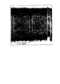
- each of the two communication nodes transmits a signal at the same time, so when observing a signal waveform using a waveform observer such as an oscilloscope, the two signal waveforms are observed in an overlapping state. Is done. For this reason, the eye pattern formed by the signal transmitted by each communication node becomes very difficult to see, and it may be difficult to evaluate the quality of the waveform. If waveform distortion or the like caused by transmission of signals through a cable is added to the signal overlap as described above, the waveform actually observed on the oscilloscope screen is, for example, random noise as shown in FIG. Waveform.
- one communication node performs communication in synchronization with the clock signal, and reproduces and transmits the clock signal included in the signal received by the other communication node, If transmission by one communication node is stopped, the other communication node cannot reproduce the clock signal, and jitter increases. Therefore, the quality of the waveform in a state where full duplex communication is performed cannot be properly evaluated.
- An object of the present disclosure is to provide a waveform observation system and a waveform observation method capable of more easily observing a signal waveform of a transmission line in which full duplex communication is performed using a differential signal.
- the reproduced clock A signal is transmitted in synchronization with the signal.
- the signal generation unit continuously displays symbols indicated by signals output to the transmission line.
- a trigger signal is output to the waveform observer at the timing when two or more are the same.
- a change point of a signal waveform transmitted from another communication node always enters between two consecutive symbols having the same value transmitted from one of the communication nodes. Therefore, the signal waveform can be easily observed in a state where full-duplex communication is performed, and the waveform quality can be appropriately evaluated.
- the configuration of the present invention is applied to observe the signal waveform. Can be easily.
- the waveform adjustment function provided in the communication node is stopped when the communication signal waveform is observed.
- the waveform adjustment function adjusts the transmission signal waveform for the purpose of reducing the occurrence of noise, and as a result, the level indicated by the waveform becomes multivalued, making observation difficult. Accordingly, the observation is facilitated by stopping the waveform adjustment function when observing the waveform.
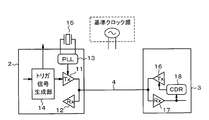
- FIG. 1 is a functional block diagram showing a configuration of a waveform observation system in the first embodiment
- FIG. 2 is a diagram schematically showing the internal configuration of the master node and the slave node.
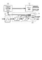
- FIG. 3 is a functional block diagram schematically showing a configuration centering on the trigger signal generation unit
- FIG. 4 is a diagram schematically showing the differential signal waveform observed on the oscilloscope screen when the signal level for two symbols is (0, 0).
- FIG. 5 is a diagram schematically showing a differential signal waveform observed on the oscilloscope screen when the signal level is (+1, +1).
- FIG. 1 is a functional block diagram showing a configuration of a waveform observation system in the first embodiment
- FIG. 2 is a diagram schematically showing the internal configuration of the master node and the slave node.
- FIG. 3 is a functional block diagram schematically showing a configuration centering on the trigger signal generation unit
- FIG. 4 is a diagram schematically showing the differential signal waveform observed on the oscilloscope screen when the
- FIG. 6 is a diagram schematically showing a differential signal waveform observed on the oscilloscope screen when the signal level is ( ⁇ 1, ⁇ 1).
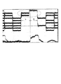
- FIG. 7 is a diagram illustrating a case where the signal waveform corresponding to FIG. 5 is observed on an actual oscilloscope screen.
- FIG. 8 is a diagram showing a case where the signal waveform corresponding to FIG. 5 is observed on an actual oscilloscope screen in the state of full duplex communication.
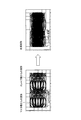
- FIG. 9 is a diagram (part 1) for explaining the pulse shaping function in the second embodiment.
- FIG. 10 is a diagram (part 2) for explaining the pulse shaping function.
- FIG. 11 is a diagram (part 3) for explaining the pulse shaping function.
- FIG. 12 is a functional block diagram schematically showing a configuration centering on the trigger signal generation unit, FIG.
- FIG. 13 is a diagram illustrating a case where the signal waveform corresponding to FIG. 5 is observed on an actual oscilloscope screen when the pulse shaping function is operating.
- FIG. 14 is a diagram showing a case where the signal waveform corresponding to FIG. 13 is observed on an actual oscilloscope screen in the state of full duplex communication
- FIG. 15 is a diagram illustrating a case where a signal waveform in a state of full duplex communication is observed on an actual oscilloscope screen, which explains the prior art.
- the waveform observation system 1 of the present embodiment includes two communication nodes 2 and 3, a differential transmission line 4 connecting between them, and an oscilloscope for observing the signal waveform of the transmission line 4. 5.
- the oscilloscope 5 corresponds to a waveform observer.
- the communication node 2 side functions as a master and the communication node 3 functions as a slave.
- Each of these functions may be fixed for each communication node, or each function may be set for a communication node that can be switched to any function.
- the communication node 2 is referred to as a master node 2 and the communication node 3 is referred to as a slave node 3.
- the master node 2 incorporates a trigger signal generation unit to be described later, and outputs a trigger signal for input to the oscilloscope 5 from the output terminal 6.
- the oscilloscope 5 has a differential probe 7 and a single probe 8.
- the differential probe 7 is connected to the signal lines 4+ and 4- of the transmission line 4 in order to observe the communication signal waveform.
- the single probe 8 is connected to the output terminal 6 of the master node 2 in order to input a trigger signal for observing the waveform. That is, when the master node 2 is configured as an integrated circuit or IC, the output terminal 6 is a terminal different from the terminal of the IC connected to the signal lines 4+ and 4- of the transmission line 4.
- the master node 2 includes a signal transmission driver circuit 11, a signal reception receiver circuit 12, a PLL (Phase Locked Loop) oscillation circuit 13, and a trigger signal generation unit 14.
- An oscillator 15 is connected to the PLL oscillation circuit 13 outside the master node 2, and the PLL oscillation circuit 13 is a reference clock signal generated by the oscillation operation of the oscillator 15, a differential applied from the outside, or a single end. Based on the reference clock, a clock signal having a predetermined frequency is generated and output to the driver circuit 11.
- the driver circuit 11 transmits data using a differential signal in synchronization with the clock signal input from the PLL oscillation circuit 13.
- the trigger signal generation unit 14 is disposed in the front part of the driver circuit 11 in order to generate a trigger signal to be input to the oscilloscope 5.
- the slave node 3 includes a driver circuit 16 for signal transmission, a receiver circuit 17 for signal reception, and a CDR (Clock Data Recovery) circuit 18.
- the CDR circuit 18 reproduces the transmission signal from the master node 2 received via the transmission line 4 and the receiver circuit 17 and the clock signal included in the transmission data, and outputs it to the driver circuit 16.
- the driver circuit 16 transmits data using a differential signal in synchronization with the clock signal.
- the trigger signal generation unit 14 is arranged in the master node 2 between an encoder 21 constituting a signal transmission sequence and a multilevel signal generation circuit 22.
- the encoder 21 encodes transmission data input from a transmission data generation unit (not shown) into three levels (+1, 0, ⁇ 1) and inputs the encoded data to the trigger signal generation unit 14.
- the trigger signal generation unit 14 includes two D flip-flops 23 and 24 connected in series, and a determination circuit 25.
- the D flip-flops 23 and 24 are configured to be compatible with three levels (+1, 0, ⁇ 1), and a clock signal output from the PLL oscillation circuit 13 is given to these clock terminals.
- the determination circuit 25 is a magnitude comparator, compares the data values of the output terminals Q of the D flip-flops 23 and 24, and outputs a trigger signal when both coincide.
- the output terminal Q of the D flip-flop 24 is connected to the input terminal of the multilevel signal generation circuit 22.
- the multi-value signal generation circuit 22 is composed of a D / A converter, and outputs an analog signal corresponding to the input three-level data value to the driver circuit 11.
- the driver circuit 11 drives the transmission line 4 so as to output a differential signal corresponding to the level of the input analog signal.
- FIG. 4 to 6 show the oscilloscope 5 when the signal level and data value for two symbols transmitted by the master node 2 are (0, 0), (+1, +1), and (-1, -1), respectively.
- the differential signal waveform observed on the screen is shown as a model.
- FIG. 7 shows the differential signal waveform on the transmission side and the trigger signal waveform actually observed on the screen of the oscilloscope 5 for the case of the signal level (+1, +1) shown in FIG.
- the transmission symbol rate of the master node 2 and the transmission symbol rate of the slave node 3 are the same, if the master node 2 transmits two symbols of the same level, the slave node 3 must always be between those two symbols.
- the change point of the transmitted symbol is entered. However, the position of the change point changes depending on the remainder obtained by dividing the cable length of the transmission line 4 by one symbol time.
- the trigger signal waveform rises near the middle of two symbols of the same level.
- FIG. 8 shows the differential signal waveform and the trigger signal waveform that are actually observed on the screen of the oscilloscope 5 together with the signal waveform transmitted by the slave node 3, that is, in the full duplex communication state. Compared to FIG. 15, the oscilloscope 5 is triggered in a state where the eye pattern can be clearly observed.
- the communication node 2 transmits a signal in synchronization with the clock signal generated by the PLL oscillation circuit 13, and the communication node 3 receives the clock signal included in the received signal.
- the signal is reproduced by the CDR circuit 18 and transmitted in synchronization with the reproduced clock signal.
- the trigger signal generation unit 14 is indicated by a signal output to the transmission line 4.
- a trigger signal is output to the oscilloscope 5 at the timing when two symbols are identical.
- the change point of the signal waveform transmitted from the communication node 3 since the change point of the signal waveform transmitted from the communication node 3 always enters between two consecutive symbols having the same value transmitted from the communication node 2, full-duplex communication is performed.
- the signal waveform can be easily observed in a state where the waveform is present, and the waveform quality can be appropriately evaluated.
- the differential signal transmitted between the communication nodes 2 and 3 shows a multilevel multilevel signal level, and the signal waveform to be observed becomes more complicated, the signal waveform is observed. Can be made easier.
- the trigger signal generation unit 14 is arranged in the master node 2 that generates a clock signal and outputs it to the transmission line 4, the trigger signal can be generated with high accuracy at a timing based on the clock signal.
- the second embodiment is based on the premise that the master node side has a pulse shaping function.
- the pulse shaping function is a technology that dares to dull the output waveform for the purpose of reducing noise.
- IEEE P802.3ab http://grouper.ieee.org/groups/802/3/ab/public/index.html It is used in.
- a pulse shaping generation circuit 32 is inserted between the output terminal Q of the D flip-flop 24 and the input terminal of the multilevel signal generation circuit 22. Yes.
- the filter function of the pulse shaping generation circuit 32 can be invalidated by a control signal given from outside. That is, the pulse shaping function can be turned off by setting the coefficient of the above-mentioned filter expression “0.75 + 0.25z ⁇ 1” to “1 + 0 ⁇ z ⁇ 1”.
- the pulse shaping function corresponds to the waveform adjustment function.
- the pulse shaping function When the pulse shaping function is applied to the case of the signal level (+1, +1) shown in FIG. 7, the signal level in the section A is divided as shown in FIG. It is a level. Which part of the eye pattern is located in these sections A and B depends on the symbol rate and the cable length, and is not suitable for waveform quality evaluation.
- the communication signal waveform is observed by the oscilloscope 5 as described above, a command is input from the outside to the master node 31 to stop and turn off the pulse shaping function.
- the actually observed waveform is as shown in FIG. 14, and the oscilloscope 5 is triggered in a state where the eye pattern is clear.
- the pulse shaping function provided in the master node 31 is stopped. Therefore, the waveform can be easily observed.
- the differential signal may be a signal that transmits a multilevel of four or more levels, or a signal that transmits a binary level of (1, 0).
- the trigger signal generation unit is not necessarily arranged inside the communication node, and may be arranged outside.
Landscapes
- Engineering & Computer Science (AREA)
- Signal Processing (AREA)
- Computer Networks & Wireless Communication (AREA)
- Physics & Mathematics (AREA)
- General Physics & Mathematics (AREA)
- General Engineering & Computer Science (AREA)
- Quality & Reliability (AREA)
- Power Engineering (AREA)
- Nonlinear Science (AREA)
- Dc Digital Transmission (AREA)
Abstract
本開示の波形観測システムは、差動信号により通信が行われる伝送線路(4)を介して全2重通信を行う2つの通信ノード(2,3)と、トリガ信号が入力されたタイミングで、前記伝送線路の通信信号波形を観測する波形観測器(5)と、前記トリガ信号を出力する信号生成部(14)とを備え、前記2つの通信ノードの一方は、自身が生成したクロック信号に同期して信号を送信し、前記2つの通信ノードの他方は、受信した信号に含まれているクロック信号を再生すると、再生したクロック信号に同期して信号を送信し、前記信号生成部は、前記伝送線路に出力される信号で示されるシンボルが連続して2つ以上同一となったタイミングで、前記トリガ信号を出力する。
Description
本出願は、2016年2月5日に出願された日本出願番号2016-20767号に基づくもので、ここにその記載内容を援用する。
本開示は、2つの通信ノードが、差動信号により通信が行われる伝送線路を介して全2重通信を行う際に、前記伝送線路の通信信号波形を観測するためのシステム及び方法に関する。
差動信号により高速で通信が行われる伝送線路について、ジッタ等の影響による通信信号波形の品質を評価する手法として、例えば特許文献1に開示されているように、アイパターン,アイダイアグラムを用いるものがある。
全2重通信が行われる伝送線路では、2つの通信ノードのそれぞれが同時に信号を送信するので、オシロスコープ等の波形観測器を用いて信号波形を観測すると、2つの信号波形が重なった状態で観測される。このため、各通信ノードが送信した信号により形成されるアイパターンが非常に見辛くなり、波形の品質を評価するのが困難となる場合がある。上記のような信号の重なりに、信号がケーブルを介して伝送されることで生じる波形歪等も加わると、実際にオシロスコープの画面上で観測される波形は、例えば図15に示すようにランダムノイズ的な波形となる。
特に、一方の通信ノードがクロック信号を生成し、そのクロック信号に同期して通信を行い、他方の通信ノードが受信した信号に含まれているクロック信号を再生して送信を行うシステムでは、一方の通信ノードによる送信を停止すれば他方の通信ノードがクロック信号を再生できずジッタが増大する。したがって、全2重通信が行われている状態での波形の品質を適切に評価できなくなる。
本開示は、差動信号により全2重通信が行われる伝送線路の信号波形をより容易に観測できる波形観測システム及び波形観測方法を提供することを目的とする。
本開示の一態様によれば、通信ノードの一方は、自身が生成したクロック信号に同期して信号を送信し、他方は、受信した信号に含まれているクロック信号を再生すると、再生したクロック信号に同期して信号を送信する。このような通信ノード間で全2重通信が行われる伝送線路について、波形観測器により通信信号波形を観測するため、信号生成部は、伝送線路に出力される信号で示されるシンボルが連続して2つ以上同一となったタイミングで波形観測器にトリガ信号を出力する。
本開示の一態様によれば、通信ノードの一方は、自身が生成したクロック信号に同期して信号を送信し、他方は、受信した信号に含まれているクロック信号を再生すると、再生したクロック信号に同期して信号を送信する。このような通信ノード間で全2重通信が行われる伝送線路について、波形観測器により通信信号波形を観測するため、信号生成部は、伝送線路に出力される信号で示されるシンボルが連続して2つ以上同一となったタイミングで波形観測器にトリガ信号を出力する。
このように構成すれば、通信ノードの1つより送信される最小で2つ連続する同一値のシンボル間には、必ず他の通信ノードが送信した信号波形の変化点が入るようになる。したがって、全2重通信が行われている状態での信号波形の観測が容易になり、波形の品質評価を適切に行うことができる。
また、本開示の一態様によれば、差動信号が多値レベルを示すことにより、観測対象となる信号波形がより複雑となる場合に、本発明の構成を適用して信号波形の観測を容易にすることができる。
また、本開示の一態様によれば、通信信号波形を観測する際に、通信ノードが備えている波形調整機能を停止させる。すなわち、波形調整機能は、ノイズの発生を低減する目的で送信信号波形を調整するので、その結果、波形が示すレベルが多値化して観測が困難になる。したがって、波形を観測する際に波形調整機能を停止させることで観測が容易になる。
本開示についての上記目的およびその他の目的、特徴や利点は、添付の図面を参照しながら下記の詳細な記述により、より明確になる。その図面は、
図1は、第1実施形態において、波形観測システムの構成を示す機能ブロック図であり、
図2は、マスタノード,スレーブノードの内部構成を概略的に示す図であり、
図3は、トリガ信号生成部を中心とする構成を概略的に示す機能ブロック図であり、
図4は、2シンボル分の信号レベルが(0,0)となる場合に、オシロスコープの画面上で観測される差動信号波形をモデル的に示す図であり、
図5は、同信号レベルが(+1,+1)となる場合に、オシロスコープの画面上で観測される差動信号波形をモデル的に示す図であり、
図6は、同信号レベルが(-1,-1)となる場合に、オシロスコープの画面上で観測される差動信号波形をモデル的に示す図であり、
図7は、図5に対応する信号波形を、実際のオシロスコープの画面上で観測した場合を示す図であり、
図8は、図5に対応する信号波形を全2重通信の状態で、実際のオシロスコープの画面上で観測した場合を示す図であり、
図9は、第2実施形態において、パルス・シェーピング機能を説明する図(その1)であり、
図10は、パルス・シェーピング機能を説明する図(その2)であり、
図11は、パルス・シェーピング機能を説明する図(その3)であり、
図12は、トリガ信号生成部を中心とする構成を概略的に示す機能ブロック図であり、
図13は、パルス・シェーピング機能が作用している場合に、図5に対応する信号波形を、実際のオシロスコープの画面上で観測した場合を示す図であり、
図14は、図13に対応する信号波形を全2重通信の状態で、実際のオシロスコープの画面上で観測した場合を示す図であり、
図15は、従来技術を説明する、全2重通信の状態の信号波形を、実際のオシロスコープの画面上で観測した場合を示す図である。
(第1実施形態)
図1に示すように、本実施形態の波形観測システム1は、2つの通信ノード2及び3と、これらの間を接続する差動の伝送線路4と、伝送線路4の信号波形を観測するオシロスコープ5とを有している。オシロスコープ5は波形観測器に相当する。本実施形態では、例えば通信ノード2側がマスタ,通信ノード3がスレーブとして機能する。これらの各機能は通信ノード毎に固定であっても良いし、何れの機能にも切り替えが可能な通信ノードにそれぞれ機能設定を行って使用しても良い。以下、通信ノード2をマスタノード2と称し、通信ノード3をスレーブノード3と称する。
図1に示すように、本実施形態の波形観測システム1は、2つの通信ノード2及び3と、これらの間を接続する差動の伝送線路4と、伝送線路4の信号波形を観測するオシロスコープ5とを有している。オシロスコープ5は波形観測器に相当する。本実施形態では、例えば通信ノード2側がマスタ,通信ノード3がスレーブとして機能する。これらの各機能は通信ノード毎に固定であっても良いし、何れの機能にも切り替えが可能な通信ノードにそれぞれ機能設定を行って使用しても良い。以下、通信ノード2をマスタノード2と称し、通信ノード3をスレーブノード3と称する。
マスタノード2は、後述するトリガ信号生成部を内蔵しており、オシロスコープ5に入力するためのトリガ信号を出力端子6より出力する。オシロスコープ5は、差動プローブ7と、シングルプローブ8とを有している。差動プローブ7は、通信信号波形を観測するため伝送線路4の信号線4+,4-に接続されている。シングルプローブ8は、上記波形を観測するためのトリガ信号を入力するため、マスタノード2の出力端子6に接続されている。すなわち、マスタノード2が集積回路,ICとして構成される際に、出力端子6は、伝送線路4の信号線4+,4-に接続されるICの端子とは異なる端子となる。
図2に示すように、マスタノード2は、信号送信用のドライバ回路11,信号受信用のレシーバ回路12,PLL(Phase Locked Loop)発振回路13及びトリガ信号生成部14を備えている。PLL発振回路13にはマスタノード2の外部で発振子15が接続されており、PLL発振回路13は、発振子15の発振動作による基準クロック信号、又は外部から印加される差動,若しくはシングルエンドの基準クロックを元に、所定周波数のクロック信号を生成してドライバ回路11に出力する。ドライバ回路11は、PLL発振回路13より入力されるクロック信号に同期して、差動信号によりデータを送信する。トリガ信号生成部14は、前述のようにオシロスコープ5に入力するトリガ信号を生成するため、ドライバ回路11の前段部分に配置されている。
一方、スレーブノード3は、信号送信用のドライバ回路16,信号受信用のレシーバ回路17及びCDR(Clock Data Recovery)回路18を備えている。CDR回路18は、伝送線路4及びレシーバ回路17を介して受信したマスタノード2からの送信信号,送信データに含まれているクロック信号を再生し、ドライバ回路16に出力する。ドライバ回路16は、前記クロック信号に同期して差動信号によりデータを送信する。
図3に示すように、トリガ信号生成部14は、マスタノード2において、信号送信系列を構成しているエンコーダ21と、多値信号生成回路22との間に配置されている。エンコーダ21は、図示しない送信データ生成部より入力される送信データを、(+1,0,-1)の3レベルにエンコードしてトリガ信号生成部14に入力する。トリガ信号生成部14は、直列に接続される2つのDフリップフロップ23及び24と、判定回路25とを有している。Dフリップフロップ23及び24は(+1,0,-1)の3レベルに対応可能に構成されており、これらのクロック端子には、PLL発振回路13より出力されるクロック信号が与えられる。
判定回路25はマグニチュードコンパレータであり、Dフリップフロップ23,24の出力端子Qのデータ値を比較し、双方が一致するとトリガ信号を出力する。Dフリップフロップ24の出力端子Qは、多値信号生成回路22の入力端子に接続されている。多値信号生成回路22はD/Aコンバータで構成され、入力される3レベルのデータ値に応じたアナログ信号をドライバ回路11に出力する。ドライバ回路11は入力されるアナログ信号のレベルに応じた差動信号を出力するように伝送線路4を駆動する。
次に、本実施形態の作用について説明する。図4~図6は、マスタノード2が送信する2シンボル分の信号レベル,データ値がそれぞれ(0,0),(+1,+1),(-1,-1)となる場合に、オシロスコープ5の画面上で観測される差動信号波形をモデル的に示している。そして、図7は、図5に示す信号レベル(+1,+1)のケースについて、実際にオシロスコープ5の画面上で観測される送信側の差動信号波形と、トリガ信号波形とを示している。
マスタノード2の送信シンボルレートと、スレーブノード3の送信シンボルレートとは同じであるから、マスタノード2が同じレベルの2シンボルを送信すれば、それらの2シンボルの間に必ず、スレーブノード3が送信したシンボルの変化点が入るようになる。但し、前記変化点の位置は、伝送線路4のケーブル長を1シンボル時間で割った余りに依存して変化する。トリガ信号波形は、同じレベルの2シンボルの中間付近で立上っている。
図8は、スレーブノード3が送信した信号波形も併せて、つまり全2重通信の状態で、実際にオシロスコープ5の画面上で観測される差動信号波形とトリガ信号波形とを示している。図15に比較して、アイパターンが明確に観測できる状態でオシロスコープ5がトリガされている。
以上のように本実施形態によれば、通信ノード2は、PLL発振回路13が生成したクロック信号に同期して信号を送信し、通信ノード3は、受信した信号に含まれているクロック信号をCDR回路18で再生し、再生したクロック信号に同期して信号を送信する。そして、通信ノード2,3間で全2重通信が行われる伝送線路4について、オシロスコープ5により通信信号波形を観測するため、トリガ信号生成部14は、伝送線路4に出力される信号で示されるシンボルが連続して2つ同一となったタイミングでオシロスコープ5にトリガ信号を出力する。
このように構成すれば、通信ノード2より送信される2つ連続する同一値のシンボル間には、必ず通信ノード3が送信した信号波形の変化点が入るので、全2重通信が行われている状態での信号波形の観測が容易になり、波形の品質評価を適切に行うことができる。そして、通信ノード2,3間で伝送される差動信号が多値レベルである3レベルを示すものに適用することで、観測対象となる信号波形がより複雑となる場合に、信号波形の観測を容易にすることができる。
また、トリガ信号生成部14を、クロック信号を生成して伝送線路4に出力するマスタノード2に配置したので、前記クロック信号に基づくタイミングでトリガ信号を高い精度で生成できる。
(第2実施形態)
以下、第1実施形態と同一部分には同一符号を付して説明を省略し、異なる部分について説明する。第2実施形態は、マスタノード側がパルス・シェーピング機能を備えていることを前提とする。パルス・シェーピング機能は、ノイズを低減する目的で出力波形を敢えて鈍らせて送信する技術であり、通信規格IEEE P802.3ab,
http://grouper.ieee.org/groups/802/3/ab/public/index.html
で用いられている。
以下、第1実施形態と同一部分には同一符号を付して説明を省略し、異なる部分について説明する。第2実施形態は、マスタノード側がパルス・シェーピング機能を備えていることを前提とする。パルス・シェーピング機能は、ノイズを低減する目的で出力波形を敢えて鈍らせて送信する技術であり、通信規格IEEE P802.3ab,
http://grouper.ieee.org/groups/802/3/ab/public/index.html
で用いられている。
そのデジタルフィルタに使用される係数は
http://opencores.org/websvn,filedetails?repname=1000basex&path=/1000base-x/trunk/doc/802.3-2008_section3.pdf
のp.212に開示されているように「0.75+0.25z-1」という式となっている。これにより3レベルの信号波形は、図9に示すように9レベルに分離することになり、重なった波形は更に複雑なものとなる。
http://opencores.org/websvn,filedetails?repname=1000basex&path=/1000base-x/trunk/doc/802.3-2008_section3.pdf
のp.212に開示されているように「0.75+0.25z-1」という式となっている。これにより3レベルの信号波形は、図9に示すように9レベルに分離することになり、重なった波形は更に複雑なものとなる。
そして、上記の信号がケーブルを介して伝送されることで高周波成分が減衰する波形歪が加わると図10に示す状態となり、これにスレーブ側の送信信号も加えて合成した波形は、図11に示す状態となる。これを実際にオシロスコープで観測した波形が、図15に示したものである。
図12に示すように、第2実施形態のマスタノード31は、Dフリップフロップ24の出力端子Qと、多値信号生成回路22の入力端子との間にパルス・シェーピング生成回路32が挿入されている。そして、パルス・シェーピング生成回路32のフィルタ機能は、外部より与える制御信号により無効化できるようになっている。すなわち、上記フィルタの式「0.75+0.25z-1」の係数を「1+0・z-1」にすることで、パルス・シェーピング機能はoffにできる。パルス・シェーピング機能は波形調整機能に相当する。
図7に示した信号レベル(+1,+1)のケースについてパルス・シェーピング機能を作用させると、図13に示すように、区間Aにおける信号レベルが分かれてしまい、区間Bにおける信号レベルも含めて3レベルとなっている。これらの区間A,Bにアイパターンのどの部分が位置するかは、シンボルレートとケーブル長とに依存するため、波形の品質評価には適さない。
そこで、第2実施形態では、上述のようにオシロスコープ5により通信信号波形を観測する際には、外部よりマスタノード31に指令を入力して、パルス・シェーピング機能を停止,offさせる。この場合、実際に観測される波形は図14に示すようになり、アイパターンが明確になる状態でオシロスコープ5がトリガされている。
以上のように第2実施形態によれば、オシロスコープ5により通信信号波形を観測する際に、マスタノード31が備えているパルス・シェーピング機能を停止させる。したがって、波形の観測が容易になる。
(その他の実施形態)
差動信号は、4レベル以上の多値レベルを伝送するものでも良く、また(1,0)の二値レベルを伝送するものでも良い。
差動信号は、4レベル以上の多値レベルを伝送するものでも良く、また(1,0)の二値レベルを伝送するものでも良い。
トリガ信号生成部は、必ずしも通信ノードの内部に配置する必要はなく、外部に配置しても良い。
本開示は、実施例に準拠して記述されたが、本開示は当該実施例や構造に限定されるものではないと理解される。本開示は、様々な変形例や均等範囲内の変形をも包含する。加えて、様々な組み合わせや形態、さらには、それらに一要素のみ、それ以上、あるいはそれ以下、を含む他の組み合わせや形態をも、本開示の範疇や思想範囲に入るものである。
本開示は、実施例に準拠して記述されたが、本開示は当該実施例や構造に限定されるものではないと理解される。本開示は、様々な変形例や均等範囲内の変形をも包含する。加えて、様々な組み合わせや形態、さらには、それらに一要素のみ、それ以上、あるいはそれ以下、を含む他の組み合わせや形態をも、本開示の範疇や思想範囲に入るものである。
Claims (9)
- 差動信号により通信が行われる伝送線路(4)を介して全2重通信を行う2つの通信ノード(2,3)と、
トリガ信号が入力されたタイミングで、前記伝送線路の通信信号波形を観測する波形観測器(5)と、
前記トリガ信号を出力する信号生成部(14)とを備え、
前記2つの通信ノードの一方は、自身が生成したクロック信号に同期して信号を送信し、
前記2つの通信ノードの他方は、受信した信号に含まれているクロック信号を再生すると、再生したクロック信号に同期して信号を送信し、
前記信号生成部は、前記伝送線路に出力される信号で示されるシンボルが連続して2つ以上同一となったタイミングで、前記トリガ信号を出力する波形観測システム。 - 前記差動信号は、多値レベルを示す請求項1記載の波形観測システム。
- 前記通信ノードが、ノイズの発生を低減するように送信信号波形を調整する波形調整機能(32)を備えていると、
前記通信信号波形を観測する際に、前記波形調整機能を停止させる請求項1又は2記載の波形観測システム。 - 前記信号生成部は、前記2つの通信ノードの何れか一方に配置されている請求項1から3の何れか一項に記載の波形観測システム。
- 前記2つの通信ノードの内、クロック信号を自身が生成する方がマスタノード(2),受信した信号に含まれているクロック信号を再生する方がスレーブノード(3)となる際に、
前記信号生成部は、前記マスタノードに配置されている請求項4記載の波形観測システム。 - 前記トリガ信号を外部に出力する端子(6)は、前記通信ノードを構成する集積回路において、前記伝送線路に接続される端子と異なっている請求項4又は5記載の波形観測システム。
- 2つの通信ノードの一方が、自身が生成したクロック信号に同期して信号を送信し、
前記2つの通信ノードの他方が、受信した信号に含まれているクロック信号を再生すると、再生したクロック信号に同期して信号を送信するもので、
これら2つの通信ノード間で、差動信号により全2重通信が行われる伝送線路の通信信号波形を、トリガ信号が入力されたタイミングで波形観測器により観測する方法であって、
前記伝送線路に出力される信号で示されるシンボルが連続して2つ以上同一となったタイミングで、前記波形観測器に前記トリガ信号を出力する波形観測方法。 - 前記差動信号が、多値レベルを示す信号である請求項7記載の波形観測方法。
- 前記通信ノードが、ノイズの発生を低減するように送信信号波形を調整する波形調整機能を備えていると、前記通信信号波形を観測する際に、前記波形調整機能を停止させる請求項7又は8記載の波形観測方法。
Priority Applications (1)
| Application Number | Priority Date | Filing Date | Title |
|---|---|---|---|
| US16/074,177 US10749643B2 (en) | 2016-02-05 | 2016-11-15 | Waveform observation system and method for waveform observation |
Applications Claiming Priority (2)
| Application Number | Priority Date | Filing Date | Title |
|---|---|---|---|
| JP2016020767A JP6424846B2 (ja) | 2016-02-05 | 2016-02-05 | 波形観測システム及び波形観測方法 |
| JP2016-020767 | 2016-02-05 |
Publications (1)
| Publication Number | Publication Date |
|---|---|
| WO2017134893A1 true WO2017134893A1 (ja) | 2017-08-10 |
Family
ID=59499478
Family Applications (1)
| Application Number | Title | Priority Date | Filing Date |
|---|---|---|---|
| PCT/JP2016/083805 Ceased WO2017134893A1 (ja) | 2016-02-05 | 2016-11-15 | 波形観測システム及び波形観測方法 |
Country Status (3)
| Country | Link |
|---|---|
| US (1) | US10749643B2 (ja) |
| JP (1) | JP6424846B2 (ja) |
| WO (1) | WO2017134893A1 (ja) |
Families Citing this family (1)
| Publication number | Priority date | Publication date | Assignee | Title |
|---|---|---|---|---|
| EP4312037A1 (en) * | 2022-07-26 | 2024-01-31 | Rohde & Schwarz GmbH & Co. KG | Measurement application device and method |
Citations (2)
| Publication number | Priority date | Publication date | Assignee | Title |
|---|---|---|---|---|
| JPH0634666A (ja) * | 1991-06-01 | 1994-02-10 | Sony Tektronix Corp | トリガ回路 |
| JP2015005962A (ja) * | 2013-06-24 | 2015-01-08 | 株式会社デンソー | データ通信システム、スレーブ及びマスタ |
Family Cites Families (2)
| Publication number | Priority date | Publication date | Assignee | Title |
|---|---|---|---|---|
| EP1460793A1 (en) | 2003-03-19 | 2004-09-22 | Synthesys Research, Inc. | A method and apparatus for counting the errors of a data signal that are outside the limits of an eye mask |
| US9503102B2 (en) * | 2014-08-29 | 2016-11-22 | Tektronix, Inc. | Synchronization for multiple arbitrary waveform generators |
-
2016
- 2016-02-05 JP JP2016020767A patent/JP6424846B2/ja not_active Expired - Fee Related
- 2016-11-15 WO PCT/JP2016/083805 patent/WO2017134893A1/ja not_active Ceased
- 2016-11-15 US US16/074,177 patent/US10749643B2/en not_active Expired - Fee Related
Patent Citations (2)
| Publication number | Priority date | Publication date | Assignee | Title |
|---|---|---|---|---|
| JPH0634666A (ja) * | 1991-06-01 | 1994-02-10 | Sony Tektronix Corp | トリガ回路 |
| JP2015005962A (ja) * | 2013-06-24 | 2015-01-08 | 株式会社デンソー | データ通信システム、スレーブ及びマスタ |
Also Published As
| Publication number | Publication date |
|---|---|
| JP6424846B2 (ja) | 2018-11-21 |
| US20190296867A1 (en) | 2019-09-26 |
| JP2017139694A (ja) | 2017-08-10 |
| US10749643B2 (en) | 2020-08-18 |
Similar Documents
| Publication | Publication Date | Title |
|---|---|---|
| US8125259B2 (en) | Duty cycle distortion (DCD) jitter modeling, calibration and generation methods | |
| US8040940B2 (en) | Transmitter/receiver device that converts serial and parallel signals and method of testing thereof | |
| US8259891B2 (en) | Adaptable phase lock loop transfer function for digital video interface | |
| US9031182B2 (en) | Method and circuit for clock recovery of a data stream description | |
| JP2009212992A (ja) | 半導体集積回路装置及びアイ開口マージン評価方法 | |
| JP4393458B2 (ja) | データ伝送装置及びデータ伝送方法 | |
| JP2010098561A (ja) | 直列信号の受信装置、直列伝送システムおよび直列伝送方法 | |
| US10079701B1 (en) | Three-valued signal generation device and three-valued signal generation method | |
| CN110995249B (zh) | 一种时钟抖动产生装置 | |
| WO2017134893A1 (ja) | 波形観測システム及び波形観測方法 | |
| JP2005233933A (ja) | 組合せ試験方法及び試験装置 | |
| JP2016063430A (ja) | 送受信回路、集積回路及び試験方法 | |
| US7692564B2 (en) | Serial-to-parallel conversion circuit and method of designing the same | |
| JP6945198B2 (ja) | クロックリカバリシステム | |
| JP2006177898A (ja) | 半導体装置および半導体装置のテスト方法 | |
| JP7068443B2 (ja) | 受信デバイス、伝送システム、自動車 | |
| JP5993197B2 (ja) | 伝送システム、伝送装置及びジッタ補償方法 | |
| JP2009539281A (ja) | クロック復元装置およびクロック復元方法 | |
| JP2006025114A (ja) | 通信装置 | |
| KR102513739B1 (ko) | Mipi d-phy 고속 송신기의 이퀄라이징 시스템 | |
| US7660364B2 (en) | Method of transmitting serial bit-stream and electronic transmitter for transmitting a serial bit-stream | |
| WO2019049198A1 (ja) | 通信回路、通信システム及び通信方法 | |
| JP4014164B2 (ja) | パルス再生回路 | |
| CN105512069B (zh) | 串行解串器装置及其异步转换方法 | |
| KR100674087B1 (ko) | Nrz 신호의 비대칭 왜곡을 이용한 클럭 신호 생성 장치 및 그를 이용한 광송수신 시스템 |
Legal Events
| Date | Code | Title | Description |
|---|---|---|---|
| 121 | Ep: the epo has been informed by wipo that ep was designated in this application |
Ref document number: 16889376 Country of ref document: EP Kind code of ref document: A1 |
|
| NENP | Non-entry into the national phase |
Ref country code: DE |
|
| 122 | Ep: pct application non-entry in european phase |
Ref document number: 16889376 Country of ref document: EP Kind code of ref document: A1 |