WO2017134713A1 - Élément électroluminescent ultraviolet - Google Patents
Élément électroluminescent ultraviolet Download PDFInfo
- Publication number
- WO2017134713A1 WO2017134713A1 PCT/JP2016/004924 JP2016004924W WO2017134713A1 WO 2017134713 A1 WO2017134713 A1 WO 2017134713A1 JP 2016004924 W JP2016004924 W JP 2016004924W WO 2017134713 A1 WO2017134713 A1 WO 2017134713A1
- Authority
- WO
- WIPO (PCT)
- Prior art keywords
- layer
- type algan
- light emitting
- ultraviolet light
- algan layer
- Prior art date
Links
Images
Classifications
-
- H—ELECTRICITY
- H01—ELECTRIC ELEMENTS
- H01L—SEMICONDUCTOR DEVICES NOT COVERED BY CLASS H10
- H01L33/00—Semiconductor devices with at least one potential-jump barrier or surface barrier specially adapted for light emission; Processes or apparatus specially adapted for the manufacture or treatment thereof or of parts thereof; Details thereof
- H01L33/02—Semiconductor devices with at least one potential-jump barrier or surface barrier specially adapted for light emission; Processes or apparatus specially adapted for the manufacture or treatment thereof or of parts thereof; Details thereof characterised by the semiconductor bodies
- H01L33/04—Semiconductor devices with at least one potential-jump barrier or surface barrier specially adapted for light emission; Processes or apparatus specially adapted for the manufacture or treatment thereof or of parts thereof; Details thereof characterised by the semiconductor bodies with a quantum effect structure or superlattice, e.g. tunnel junction
- H01L33/06—Semiconductor devices with at least one potential-jump barrier or surface barrier specially adapted for light emission; Processes or apparatus specially adapted for the manufacture or treatment thereof or of parts thereof; Details thereof characterised by the semiconductor bodies with a quantum effect structure or superlattice, e.g. tunnel junction within the light emitting region, e.g. quantum confinement structure or tunnel barrier
-
- H—ELECTRICITY
- H01—ELECTRIC ELEMENTS
- H01L—SEMICONDUCTOR DEVICES NOT COVERED BY CLASS H10
- H01L33/00—Semiconductor devices with at least one potential-jump barrier or surface barrier specially adapted for light emission; Processes or apparatus specially adapted for the manufacture or treatment thereof or of parts thereof; Details thereof
- H01L33/02—Semiconductor devices with at least one potential-jump barrier or surface barrier specially adapted for light emission; Processes or apparatus specially adapted for the manufacture or treatment thereof or of parts thereof; Details thereof characterised by the semiconductor bodies
- H01L33/26—Materials of the light emitting region
- H01L33/30—Materials of the light emitting region containing only elements of group III and group V of the periodic system
- H01L33/32—Materials of the light emitting region containing only elements of group III and group V of the periodic system containing nitrogen
Definitions
- the present invention generally relates to an ultraviolet light emitting device, and more particularly to an ultraviolet light emitting device that emits ultraviolet light.
- Patent Document 1 a p-type AlGaN layer having an Al composition ratio of 0.5 or more in an ultraviolet light emitting device
- Patent Document 1 as a p-type AlGaN layer having an Al composition ratio of 0.5 or more, p-type AlGaN doped with acceptor impurity atoms at a concentration of 5 ⁇ 10 18 cm ⁇ 3 to 1 ⁇ 10 20 cm ⁇ 3. Layers are listed.
- Patent Document 1 describes that by using the above-described p-type AlGaN layer, a light emitting diode and a laser diode that emit light in the deep ultraviolet region of 300 nm or less can be manufactured.
- An object of the present invention is to provide an ultraviolet light-emitting element capable of increasing the light output.
- An ultraviolet light-emitting device includes a stacked body in which an n-type AlGaN layer, a light-emitting layer, and a p-type AlGaN layer are arranged in this order, and the light-emitting layer on the surface of the n-type AlGaN layer on the light-emitting layer side.
- a negative electrode provided directly on a portion not covered with a positive electrode, and a positive electrode provided directly on the surface of the p-type AlGaN layer.
- the light emitting layer has a multiple quantum well structure in which a plurality of barrier layers and a plurality of well layers are alternately arranged. Each of the plurality of well layers is composed of a first AlGaN layer.
- Each of the plurality of barrier layers is constituted by a second AlGaN layer having a higher Al composition ratio than the first AlGaN layer.
- the n-type AlGaN layer has a higher Al composition ratio than the first AlGaN layer.
- the p-type AlGaN layer has a stacked structure in which a plurality of first p-type AlGaN layers and a plurality of second p-type AlGaN layers are alternately arranged.
- Each of the plurality of first p-type AlGaN layers has an Al composition ratio larger than that of the first AlGaN layer and contains Mg.
- Each of the plurality of second p-type AlGaN layers has a higher Al composition ratio than the first AlGaN layer and contains Mg at a higher concentration than each of the plurality of first p-type AlGaN layers. is doing.
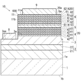
- FIG. 1 is a schematic cross-sectional view of an ultraviolet light emitting device according to an embodiment of the present invention.
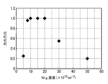
- FIG. 2 is a graph showing the relationship between the Mg concentration and the light output ratio of an ultraviolet light emitting device having a p-type AlGaN layer having a single layer structure.
- FIG. 1 described in the following embodiment is a schematic diagram, and the ratio of the size and thickness of each component in FIG. 1 does not necessarily reflect the actual dimensional ratio.
- the ultraviolet light-emitting element 10 includes a laminate 20 in which an n-type AlGaN layer 3, a light-emitting layer 4, and a p-type AlGaN layer 6 are arranged in this order.
- the ultraviolet light emitting element 10 includes a negative electrode 8 directly provided on a portion 3aa of the n-type AlGaN layer 3 on the light emitting layer 4 side that is not covered with the light emitting layer 4, and a surface of the p-type AlGaN layer 6. And a positive electrode 9 provided directly on 6a.
- the light emitting layer 4 has a multiple quantum well structure in which a plurality of barrier layers 42 and a plurality of well layers 41 are alternately arranged.
- Each of the plurality of well layers 41 is composed of a first AlGaN layer.
- Each of the plurality of barrier layers 42 is composed of a second AlGaN layer having a higher Al composition ratio than the first AlGaN layer.
- the first AlGaN layer and the second AlGaN layer are undoped AlGaN layers.
- the first AlGaN layer and the second AlGaN layer may contain impurities such as Mg, H, Si, C, and O that are inevitably mixed during each growth.
- the concentration of impurities is a value measured by secondary ion mass spectroscopy (SIMS).
- the Mg concentration is 1 ⁇ 10 17 cm ⁇ 3
- the H concentration is 1 ⁇ 10 18 cm ⁇ 3
- the Si concentration is 2 ⁇ 10 17 cm ⁇ 3
- the C concentration was 7 ⁇ 10 16 cm ⁇ 3 and the concentration of O was 7 ⁇ 10 16 cm ⁇ 3 , but the concentration of these impurities is not limited to the above values.
- the Mg concentration is 5 ⁇ 10 17 cm ⁇ 3 or less
- the H concentration is 2 ⁇ 10 18 cm ⁇ 3 or less
- the Si concentration is 5 ⁇ 10 17 cm ⁇ 3 or less
- the concentration of C is 3 ⁇ 10 17 cm ⁇ 3 or less
- the concentration of O is 3 ⁇ 10 17 cm ⁇ 3 or less.
- the n-type AlGaN layer 3 is doped with Si at the time of growth, and contains Si.
- the p-type AlGaN layer 6 has a stacked structure in which a plurality of first p-type AlGaN layers 61 and a plurality of second p-type AlGaN layers 62 are alternately arranged.
- the plurality of first p-type AlGaN layers 61 and the plurality of second p-type AlGaN layers 62 are doped with Mg at the time of growth, and contain Mg.
- the ultraviolet light emitting element 10 further includes a substrate 1 that supports the laminate 20.
- the stacked body 20 is provided on one surface 1 a of the substrate 1.
- the n-type AlGaN layer 3, the light emitting layer 4, and the p-type AlGaN layer 6 are arranged in this order from one surface 1a of the substrate 1.
- the stacked body 20 preferably includes the buffer layer 2 interposed between the substrate 1 and the n-type AlGaN layer 3.
- the ultraviolet light emitting element 10 preferably includes an electron blocking layer 5 between the light emitting layer 4 and the p-type AlGaN layer 6.
- the electron blocking layer 5 is a layer for blocking electrons from the light emitting layer 4 side in the thickness direction of the stacked body 20.
- the ultraviolet light emitting element 10 has a mesa structure 11.
- the mesa structure 11 includes a part of the stacked body 20 including the buffer layer 2, the n-type AlGaN layer 3, the light emitting layer 4, the electron blocking layer 5, and the p-type AlGaN layer 6, and the n-type AlGaN from the surface 20 a side of the stacked body 20. It is formed by etching partway through the layer 3.
- the surface 6 a of the p-type AlGaN layer 6, the surface 20 a of the stacked body 20, and the upper surface 11 a of the mesa structure 11 are configured by the same surface.
- the negative electrode 8 is directly provided on the portion 3 aa of the n-type AlGaN layer 3 on the light emitting layer 4 side which is not covered with the light emitting layer 4, and the surface 6 a of the p-type AlGaN layer 6 is formed.
- the positive electrode 9 is directly provided.
- the negative electrode 8 and the positive electrode 9 are arranged on one surface side in the thickness direction of the ultraviolet light emitting element 10.
- one surface in the thickness direction of the ultraviolet light-emitting element 10 means the surface 3 a of the n-type AlGaN layer 3 on the light-emitting layer 4 side that is not covered with the light-emitting layer 4 and the surface of the p-type AlGaN layer 6. 6a is included.
- the surface 3a of the n-type AlGaN layer 3 there is a step between the portion covered with the light emitting layer 4 and the portion 3aa not covered.
- the negative electrode 8 is electrically connected to the n-type AlGaN layer 3.
- the n-type AlGaN layer 3 for transporting electrons to the light-emitting layer 4 also serves as an n-type contact layer.
- the positive electrode 9 is electrically connected to the p-type AlGaN layer 6.
- the p-type AlGaN layer 6 for transporting holes to the light-emitting layer 4 also serves as a p-type contact layer.
- an electrically insulating film (a portion of the upper surface 11 a of the mesa structure 11, the side surface 11 b of the mesa structure 11, and the portion 3 aa of the surface 3 a of the n-type AlGaN layer 3 not covered with the light emitting layer 4) (Not shown) is preferably formed.
- the material of the electrical insulating film is, for example, SiO 2 or the like.
- the composition ratio is a value obtained by composition analysis by the EDX method (energy-dispersive-X-ray-spectroscopy).
- the composition ratio is not limited to the EDX method, and may be a value obtained by composition analysis by Auger electron spectroscopy (auger electron spectroscopy), for example.
- the depth profile of the Mg concentration is a depth profile measured by SIMS.
- the ultraviolet light emitting element 10 is a rectangular parallelepiped LED chip (light emitting diode chip).
- the LED chip is also called an LED die (light emitting diode).
- the planar view shape of the ultraviolet light emitting element 10 is, for example, a square shape.
- the “planar shape of the ultraviolet light emitting element 10” is an outer peripheral shape of the ultraviolet light emitting element 10 as viewed from one direction of the thickness direction of the ultraviolet light emitting element 10.
- the chip size of the ultraviolet light emitting element 10 in a plan view is, for example, 400 ⁇ m ⁇ (400 ⁇ m ⁇ 400 ⁇ m).
- the chip size of the ultraviolet light emitting element 10 is not limited to 400 ⁇ m ⁇ (400 ⁇ m ⁇ 400 ⁇ m), and can be appropriately set within a range of, for example, about 200 ⁇ m ⁇ (200 ⁇ m ⁇ 200 ⁇ m) to 1 mm ⁇ (1 mm ⁇ 1 mm).
- the planar view shape of the ultraviolet light emitting element 10 is not limited to a square shape, and may be, for example, a rectangular shape.
- the ultraviolet light emitting element 10 is configured with the well layer 41 of the light emitting layer 4 so as to emit ultraviolet rays in the UV-C wavelength region.
- the “UV-C wavelength range” is, for example, 100 nm to 280 nm according to the classification by the wavelength of ultraviolet rays in the International Commission on Illumination (CIE).
- CIE International Commission on Illumination
- the Al composition ratio in the first AlGaN layer constituting the well layer 41 is 0.45.
- the emission peak wavelength of the ultraviolet light emitting element 10 is 275 nm.
- the “emission peak wavelength” here is the main emission peak wavelength at room temperature (27 ° C.).
- the “emission peak wavelength of the ultraviolet light emitting element 10” is an emission peak wavelength of ultraviolet light emitted from the light emitting layer 4 and emitted from the ultraviolet light emitting element 10.
- the substrate 1 supporting the laminate 20 in the ultraviolet light emitting element 10 is a sapphire substrate.
- One surface 1a (hereinafter also referred to as “first surface 1a”) of the substrate 1 is preferably a (0001) plane, that is, a c-plane.
- the first surface 1a of the substrate 1 preferably has an off angle from the (0001) plane of 0 ° to 0.4 °, more preferably 0.1 ° to 0.31 °, More preferably, the angle is 0.21 ° to 0.31 °.
- the “off angle” is an inclination angle of the first surface 1a with respect to the (0001) plane. Therefore, if the off-angle is 0 °, the first surface 1a is a (0001) surface.
- the second surface 1 b opposite to the first surface 1 a in the substrate 1 constitutes a light extraction surface that emits ultraviolet light.
- the thickness of the substrate 1 is preferably about 100 ⁇ m to 500 ⁇ m, for example.
- substrate 1 is not restricted to c surface, For example, m surface, a surface, R surface etc. may be sufficient.
- the stacked body 20 can be formed by an epitaxial growth method.
- a MOVPE metal organic vapor phase epitaxy
- the epitaxial growth method is not limited to the MOVPE method, and for example, an HVPE (hydride vapor phase epitaxy) method, MBE (molecular beam epitaxy) method, or the like may be employed.
- the ultraviolet light emitting element 10 preferably includes a buffer layer 2 interposed between the substrate 1 and the n-type AlGaN layer 3.
- the n-type AlGaN layer 3 is preferably formed on the one surface 1 a of the substrate 1 via the buffer layer 2.
- the buffer layer 2 is a layer provided for the purpose of improving the crystallinity of the n-type AlGaN layer 3, the light emitting layer 4, the electron block layer 5, and the p-type AlGaN layer 6.
- the ultraviolet light emitting element 10 can reduce the dislocation density and improve the crystallinity of the n-type AlGaN layer 3, the light-emitting layer 4, the electron block layer 5, and the p-type AlGaN layer 6. It becomes possible to plan. Therefore, the ultraviolet light emitting element 10 can improve the light emission efficiency.
- the buffer layer 2 includes a first buffer layer 21 that is directly formed on the one surface 1 a of the substrate 1 and a second buffer layer 22 that is directly formed on the first buffer layer 21.
- the first buffer layer 21 is preferably composed of, for example, an AlN layer.
- the second buffer layer 22 is composed of an AlGaN layer having a higher Al composition ratio than the n-type AlGaN layer 3 and a smaller lattice constant difference from the first buffer layer 21 than the n-type AlGaN layer 3. More specifically, the second buffer layer 22 is composed of an AlGaN layer having an Al composition ratio of 0.90 (that is, an Al 0.90 Ga 0.10 N layer).
- the thickness of the first buffer layer 21 is preferably 3 ⁇ m or more and 6 ⁇ m or less, for example.
- the thickness of the second buffer layer 22 is preferably not less than 30 nm and not more than 100 nm, for example.
- the buffer layer 2 may be constituted only by the first buffer layer 21.
- the band gap energy of each of the first buffer layer 21 and the second buffer layer 22 is larger than the band gap energy of each of the plurality of well layers 41 in the light emitting layer 4.
- the n-type AlGaN layer 3 is a layer for transporting electrons to the light emitting layer 4.
- the Al composition ratio of the n-type AlGaN layer 3 is preferably set so that the absorption of ultraviolet rays emitted from the light-emitting layer 4 in the n-type AlGaN layer 3 is suppressed.
- the Al composition ratio of the well layer 41 is 0.45 and the Al composition ratio of the barrier layer 42 is 0.60
- the Al composition ratio of the n-type AlGaN layer 3 is equal to the Al composition ratio of the barrier layer 42. It is the same 0.60.
- the Al composition ratio of the n-type AlGaN layer 3 is not limited to the same as the Al composition ratio of the barrier layer 42 but may be different.
- the Al composition ratio of the n-type AlGaN layer 3 is preferably 0.50 or more and 0.70 or less.
- the ultraviolet light emitting element 10 when the Al composition ratio of the n-type AlGaN layer 3 is less than 0.50, the ultraviolet light emitted from the light emitting layer 4 is easily absorbed by the n-type AlGaN layer 3, and the light extraction efficiency is reduced.
- the Al composition ratio of the n-type AlGaN layer 3 is larger than 0.70, the lattice constant difference between the n-type AlGaN layer 3 and the light-emitting layer 4 becomes large, and the light-emitting layer 4 has a defect. Is likely to occur.
- the n-type AlGaN layer 3 contains Si.
- the n-type AlGaN layer 3 also serves as an n-type contact layer for realizing good ohmic contact with the negative electrode 8.
- the Si concentration in the n-type AlGaN layer 3 is preferably 5 ⁇ 10 18 cm ⁇ 3 or more and 5 ⁇ 10 19 cm ⁇ 3 or less.
- the Si concentration of the n-type AlGaN layer 3 is less than 5 ⁇ 10 18 cm ⁇ 3 , the ultraviolet light emitting element 10 cannot form an ohmic contact between the negative electrode 8 and the n-type AlGaN layer 3, or the ohmic property is lowered. Resulting in. Further, in the ultraviolet light emitting element 10, when the Si concentration of the n-type AlGaN layer 3 is higher than 5 ⁇ 10 19 cm ⁇ 3 , the crystallinity of the n-type AlGaN layer 3 is lowered.
- the thickness of the n-type AlGaN layer 3 is preferably 1 ⁇ m or more and 3 ⁇ m or less, for example.
- the ultraviolet light emitting element 10 has the mesa structure 11 described above, and the negative electrode 8 and the positive electrode 9 are arranged on one surface side in the thickness direction of the ultraviolet light emitting element 10. If it is less than 1 ⁇ m, the current path in the n-type AlGaN layer 3 becomes narrow, and the drive voltage becomes high. In the ultraviolet light emitting element 10, when the thickness of the n-type AlGaN layer 3 is larger than 3 ⁇ m, cracks may occur due to accumulation of strain in the n-type AlGaN layer 3.
- the n-type AlGaN layer 3 is not limited to a single layer structure, and may be a stacked structure of a plurality of n-type AlGaN layers having different Al composition ratios.
- the light emitting layer 4 between the n-type AlGaN layer 3 and the p-type AlGaN layer 6 in the thickness direction of the stacked body 20 is caused by recombination of two types of carriers (electrons and holes) injected into the well layer 41. It is a layer that emits light (ultraviolet rays).
- the light emitting layer 4 a plurality of barrier layers 42 and a plurality of well layers 41 are alternately arranged in the thickness direction of the stacked body 20. Thereby, the light emitting layer 4 has a multiple quantum well structure.
- the light emitting layer 4 in the ultraviolet light emitting element 10 includes four well layers 41 and four barrier layers 42.
- the light emitting layer 4 can set the light emission peak wavelength to an arbitrary light emission peak wavelength in the range of 210 nm to 360 nm by changing the Al composition ratio of the first AlGaN layer constituting the well layer 41. .
- the light emitting layer 4 includes a well layer 41 that emits ultraviolet rays in the UV-C wavelength region.
- the well layer 41 has an Al composition ratio of 0.45 so that the emission peak wavelength of the ultraviolet light emitting element 10 is, for example, 275 nm. That is, the first AlGaN layer is an Al 0.45 Ga 0.55 N layer.
- the Al composition ratio of the second AlGaN layer constituting the barrier layer 42 is 0.60. That is, the second AlGaN layer is an Al 0.60 Ga 0.40 N layer.
- the thickness of each of the plurality of well layers 41 is preferably not less than 0.5 nm and not more than 3 nm.
- the ultraviolet light emitting element 10 tends to decrease the light emission efficiency when the thickness of the well layer 41 is less than 0.5 nm. This is presumably because when the thickness of the well layer 41 is less than 0.5 nm, the carrier confinement effect of the light emitting layer 4 is reduced. Moreover, the ultraviolet light emitting element 10 has a tendency that the light emission efficiency is lowered when the thickness of the well layer 41 is larger than 3 nm.
- each of the plurality of barrier layers 42 is preferably 2 nm or more and 20 nm or less.
- the thickness of the barrier layer 42 is less than 2 nm, the carrier confinement effect that carriers are confined in the well layer 41 by the barrier layer 42 is reduced, and the carriers easily leak from the well layer 41 and emit light. It is assumed that the efficiency will decrease. Further, in the ultraviolet light emitting element 10, there is a concern that carriers are not injected into the well layer 41 when the thickness of the barrier layer 42 is larger than 20 nm.
- the second AlGaN layer constituting the barrier layer 42 is an undoped AlGaN layer, but is not limited thereto, and may contain Si (or a Si-doped AlGaN layer).
- the Si concentration is preferably 5 ⁇ 10 17 cm ⁇ 3 or more and 5 ⁇ 10 18 cm ⁇ 3 or less.
- the ultraviolet light emitting element 10 can relieve the distortion generated by the piezo electric field due to the lattice mismatch, and the light emission efficiency can be improved.
- the Si concentration of the barrier layer 42 when the Si concentration of the barrier layer 42 is less than 5 ⁇ 10 17 cm ⁇ 3, the effect of alleviating the strain generated by the piezoelectric field is reduced.
- the Si concentration of the barrier layer 42 is higher than 5 ⁇ 10 18 cm ⁇ 3 , the crystallinity of the barrier layer 42 tends to decrease.
- the electron blocking layer 5 provided between the light emitting layer 4 and the p-type AlGaN layer 6 has a function of blocking electrons from the light emitting layer 4 side.
- the electron blocking layer 5 among the electrons injected from the n-type AlGaN layer 3 into the light emitting layer 4, electrons not recombined with holes in the light emitting layer 4 leak to the p-type AlGaN layer 6 ( This is a layer for suppressing overflow).
- the electron blocking layer 5 is interposed between the light emitting layer 4 and the first p-type AlGaN layer 61 (610) closest to the light emitting layer 4 in the p-type AlGaN layer 6.
- the electron block layer 5 is composed of a third p-type AlGaN layer.
- the third p-type AlGaN layer has an Al composition ratio larger than each of the first p-type AlGaN layer 61 and the second p-type AlGaN layer 62 of the p-type AlGaN layer 6 and contains Mg. .
- the Al composition ratio of the third p-type AlGaN layer is 0.90, but is not limited to this value.
- the thickness of the electron blocking layer 5 cannot be generally specified because the suitable thickness varies depending on the Al composition ratio, Mg concentration, etc. of the electron blocking layer 5, but is preferably 1 nm to 50 nm. More preferably, it is 25 nm.
- the Mg concentration of the electron block layer 5 is preferably lower than the Mg concentration of each of the first p-type AlGaN layer 61 and the second p-type AlGaN layer 62 of the p-type AlGaN layer 6. Thereby, in the ultraviolet light emitting element 10, the crystallinity of the electronic block layer 5 can be improved.
- the p-type AlGaN layer 6 is a layer for transporting holes to the light emitting layer 4.
- the p-type AlGaN layer 6 also serves as a p-type contact layer for realizing good ohmic contact with the positive electrode 9.
- the p-type AlGaN layer 6 has a stacked structure in which a plurality of first p-type AlGaN layers 61 and a plurality of second p-type AlGaN layers 62 are alternately arranged in the thickness direction of the stacked body 20.
- the plurality of first p-type AlGaN layers 61 and the plurality of second p-type AlGaN layers 62 are doped with Mg at the time of growth, and contain Mg.
- the p-type AlGaN layer 6 in the ultraviolet light-emitting element 10 has five first p-type AlGaN layers 61 and two second p-type AlGaN layers 62.
- the composition ratio of Al in the plurality of first p-type AlGaN layers 61 and the plurality of second p-type AlGaN layers 62 is such that each of the plurality of first p-type AlGaN layers 61 that emit ultraviolet light in the light-emitting layer 4 and the plurality of p-type AlGaN layers 61 and plural.
- the second p-type AlGaN layer 62 is preferably set so as to be able to suppress absorption. Accordingly, the Al composition ratio of each of the plurality of first p-type AlGaN layers 61 and each of the plurality of second p-type AlGaN layers 62 is higher than that of each of the plurality of well layers 41 (first AlGaN layers).
- the Al composition ratio is large, and it is more preferable that the Al composition ratio is larger than each of the plurality of barrier layers 42 (second AlGaN layers).
- the Al composition ratio of each of the plurality of well layers 41 (first AlGaN layers) is 0.45 and the Al composition ratio of each of the plurality of barrier layers 42 (second AlGaN layers) is 0.60
- the Al composition ratio of each of the plurality of first p-type AlGaN layers 61 and each of the plurality of second p-type AlGaN layers 62 is preferably, for example, 0.65.
- first AlGaN layer when each of the plurality of well layers 41 (first AlGaN layer) is composed of an Al 0.45 Ga 0.55 N layer, the first p-type AlGaN layer 61 and the second p-type AlGaN layer 62 have a Mg concentration relative to each other.
- a preferred example is a p-type Al 0.65 Ga 0.35 N layer having a different thickness.
- the plurality of first p-type AlGaN layers 61 and the plurality of second p-type AlGaN layers 62 contain Mg at a higher concentration than the electron block layer 5 (third p-type AlGaN layer).
- Each of the plurality of second p-type AlGaN layers 62 contains Mg at a higher concentration than each of the plurality of first p-type AlGaN layers 61.
- the inventors of the present application when developing the ultraviolet light emitting element 10 having the p-type AlGaN layer 6 also serving as the p-type contact layer, the inventors of the present application emit ultraviolet light of Reference Examples 1 to 7 having substantially the same basic structure as the ultraviolet light emitting element 10. An element was produced. Then, the inventors of the present application measured the light output [W] when a direct current of 20 mA was passed for each of the ultraviolet light emitting elements of Reference Examples 1 to 7.
- the ultraviolet light emitting elements of Reference Examples 1 to 7 are only described in that a single layer p-type AlGaN layer is used instead of the p-type AlGaN layer 6 having a multilayer structure in the ultraviolet light emitting element 10 of the embodiment. This is different from the ultraviolet light emitting element 10.
- the thickness of the p-type AlGaN layer having a single layer structure is 60 nm.
- the ultraviolet light emitting elements of Reference Examples 1 to 7 have different Mg concentrations in the p-type AlGaN layer. More specifically, the Mg concentration of the p-type AlGaN layer in the ultraviolet light emitting devices of Reference Examples 1, 2, 3, 4, 5, 6, and 7 is 5 ⁇ 10 19 cm ⁇ 3 and 8 ⁇ 10 19 cm, respectively. ⁇ 3 , 1 ⁇ 10 20 cm ⁇ 3 , 1.5 ⁇ 10 20 cm ⁇ 3 , 2 ⁇ 10 20 cm ⁇ 3 , 3 ⁇ 10 20 cm ⁇ 3 and 5 ⁇ 10 20 cm ⁇ 3 .
- the light output is a value measured using an integrating sphere and a spectroscope.
- FIG. 2 is a graph showing the relationship between the Mg concentration of the p-type AlGaN layer and the light output ratio.
- the “light output ratio” is a relative value based on the light output of the ultraviolet light emitting element of Reference Example 3 in which the Mg concentration is 10 ⁇ 10 19 cm ⁇ 3 (that is, 1 ⁇ 10 20 cm ⁇ 3 ). It is. From FIG.
- the inventors of the present application have determined that the Mg concentration of the p-type AlGaN layer is 8 ⁇ 10 19 cm ⁇ 3 or more and 2 ⁇ in the ultraviolet light-emitting device in which the p-type contact layer is composed of a single-layer p-type AlGaN layer. It was found that the light output can be improved by setting the Mg concentration to 5 ⁇ 10 19 cm ⁇ 3 or more by setting it to 10 20 cm ⁇ 3 or less. In addition, from FIG.
- the inventors of the present application have determined that the Mg concentration of the p-type AlGaN layer is 8 ⁇ 10 19 cm ⁇ 3 or more in the ultraviolet light-emitting device in which the p-type contact layer is composed of a single-layer p-type AlGaN layer. It was found that by making the concentration 2 ⁇ 10 20 cm ⁇ 3 or less, it becomes possible to suppress a decrease in light output when the Mg concentration is 1 ⁇ 10 20 cm ⁇ 3 .
- the inventors of the present application produced a sample for evaluation in which the Mg concentration was increased stepwise as the distance from the electron block layer in the p-type AlGaN layer having a single-layer structure was increased, and a cross-sectional transmission electron microscope was obtained. image).
- a cross-sectional TEM shows that a sample for evaluation in which the maximum value of Mg concentration in the p-type AlGaN layer is higher than 2 ⁇ 10 20 cm ⁇ 3 becomes an aggregate of columnar structure crystals. Confirmed by image.
- the thickness of the p-type AlGaN layer having a single layer structure in the evaluation sample is 60 nm.
- the inventors of the present application have determined that the maximum value of the Mg concentration in the single-layer p-type AlGaN layer is higher than 2 ⁇ 10 20 cm ⁇ 3 . It was inferred that the crystallinity of the p-type AlGaN layer having a single layer structure was lowered and the light output of the ultraviolet light emitting device was lowered.
- the p-type AlGaN layer 6 that also serves as a contact layer has a plurality of first p-type AlGaN layers 61 and a plurality of second p-type AlGaN layers 62 arranged alternately. It has a laminated structure.
- Each of the plurality of second p-type AlGaN layers 62 contains Mg at a higher concentration than each of the plurality of first p-type AlGaN layers 61.
- the ultraviolet light emitting element 10 while improving the conductivity of the p-type AlGaN layer 6 by increasing the Mg concentration of each of the plurality of second p-type AlGaN layers 62, It is possible to suppress the decrease in crystallinity and increase the light output.
- the thickness of each of the plurality of first p-type AlGaN layers 61 is preferably 5 nm or more and 20 nm or less.
- the thickness of each of the plurality of second p-type AlGaN layers 62 is preferably not less than 0.5 nm and not more than 5 nm.
- the Mg concentration of each of the plurality of first p-type AlGaN layers 61 is set to 8 ⁇ 10 19 cm ⁇ 3 or more and 2 ⁇ 10 20 cm ⁇ 3 or less, and the plurality of second p Even if the Mg concentration of each of the AlGaN layers 62 is 3 ⁇ 10 20 cm ⁇ 3 or more and 2 ⁇ 10 21 cm ⁇ 3 or less, it is possible to suppress the crystallinity of the p-type AlGaN layer 6 from being reduced. It becomes possible to increase the output.
- 0.5 nm is a value corresponding to the lattice constant of the second p-type AlGaN layer 62.
- the thickness of the p-type AlGaN layer 6 is preferably 200 nm or less, and more preferably 100 nm or less. Further, from the viewpoint of reducing the in-plane variation of the electrical characteristics of the p-type AlGaN layer 6, the thickness of the p-type AlGaN layer 6 is preferably 30 nm or more, and more preferably 50 nm or more.
- the Mg concentrations of the plurality of first p-type AlGaN layers 61 are the same, but may be different from each other. Further, the thicknesses of the plurality of first p-type AlGaN layers 61 are the same, but may be different from each other.
- the Mg concentration of the plurality of second p-type AlGaN layers 62 is the same, but may be different from each other. Further, the thicknesses of the plurality of second p-type AlGaN layers 62 are the same, but may be different from each other.
- the number of the first p-type AlGaN layers 61 is the same as the number of the second p-type AlGaN layers, but they may be different.
- the negative electrode 8 is a contact electrode formed on a portion 3aa of the surface 3a of the n-type AlGaN layer 3 that is not covered with the light emitting layer 4 in order to obtain ohmic contact with the n-type AlGaN layer 3.
- the negative electrode 8 includes a laminated film of a first Ti layer, an Al layer, a second Ti layer, and an Au layer (hereinafter also referred to as “first laminated film”) as a portion 3aa of the n-type AlGaN layer 3. It is formed by performing an annealing process after being formed thereon.
- the thicknesses of the first Ti layer, the Al layer, the second Ti layer, and the Au layer in the first stacked film are 20 nm, 50 nm, 20 nm, and 100 nm, respectively.
- the positive electrode 9 is a contact electrode formed on the surface 6 a of the p-type AlGaN layer 6 in order to obtain ohmic contact with the p-type AlGaN layer 6.
- the positive electrode 9 is formed by forming a laminated film of an Ni layer and an Au layer (hereinafter also referred to as “second laminated film”) on the surface 6 a of the p-type AlGaN layer 6 and then performing an annealing treatment. It is formed by.
- the thicknesses of the Ni layer and the Au layer in the second stacked film are 20 nm and 150 nm, respectively.
- the ultraviolet light emitting element 10 preferably includes a first pad electrode on the negative electrode 8.
- the first pad electrode is an external connection electrode.
- the first pad electrode is, for example, a laminated film of a Ti film on the negative electrode 8 and an Au film on the Ti film.
- the first pad electrode is electrically connected to the negative electrode 8.
- the first pad electrode preferably covers the negative electrode 8.
- the ultraviolet light emitting element 10 preferably includes a second pad electrode on the positive electrode 9.
- the second pad electrode is an external connection electrode.
- the second pad electrode is, for example, a laminated film of a Ti film on the positive electrode 9 and an Au film on the Ti film.
- the second pad electrode is electrically connected to the positive electrode 9.
- the second pad electrode preferably covers the positive electrode 9.
- the ultraviolet light emitting element 10 is not limited to be configured to emit ultraviolet rays in the UV-C wavelength range, and may be configured to emit ultraviolet rays in the UV-B wavelength range, for example.
- the “UV-B wavelength range” is, for example, 280 nm to 315 nm according to the classification by the wavelength of ultraviolet rays in the International Commission on Illumination.
- a wafer (sapphire wafer) serving as a base for the substrate 1 of each of the plurality of ultraviolet light emitting elements 10 is prepared.
- the wafer is introduced into an epitaxial growth apparatus, and then the stacked body 20 is stacked on the first surface of the wafer by the epitaxial growth method. .
- the first surface of the wafer is a surface corresponding to the first surface 1 a of the substrate 1.
- TMAl trimethylaluminum
- TMGa trimethyl gallium
- NH 3 is preferably employed as the N source gas.
- TESi tetraethylsilane
- Cp 2 Mg biscyclopentadienyl magnesium
- H 2 gas is preferably used as the carrier gas of each source gas.
- Each source gas is not particularly limited.
- triethylgallium (TEGa) may be employed as a Ga source gas
- hydrazine derivative may be employed as a N source gas
- monosilane (SiH 4 ) may be employed as a Si source gas.
- the growth conditions of the stacked body 20 are the first buffer layer 21, the second buffer layer 22, the n-type AlGaN layer 3, the barrier layer 42 (second AlGaN layer), the well layer 41 (first AlGaN layer), For each of the electron block layer 5 (third p-type AlGaN layer), the first p-type AlGaN layer 61, and the second p-type AlGaN layer 62, the substrate temperature, the V / III ratio, the supply amount of each source gas, and the growth What is necessary is just to set a pressure etc. suitably. “Substrate temperature” means the temperature of a wafer.
- the temperature of a susceptor that supports the wafer can be used as the “substrate temperature”.
- the temperature of the susceptor measured by a thermocouple can be substituted for the substrate temperature.
- the wafer on which the laminated body 20 is laminated is taken out from the epitaxial growth apparatus.
- a structure including at least the wafer and the stacked body 20 is referred to as an epitaxial wafer.
- the epitaxial wafer taken out from the epitaxial growth apparatus is introduced into the annealing apparatus, and the electron block layer 5, the plurality of first p-type AlGaN layers 61, and the plurality of second p-type AlGaN layers 62, respectively.
- Annealing is performed to activate the p-type impurities.
- an annealing apparatus for performing annealing for example, a lamp annealing apparatus, an electric furnace annealing apparatus, or the like can be employed.
- a p-type impurity means an acceptor impurity and is Mg.
- the mesa structure 11 is formed using a photolithography technique, an etching technique, and the like after taking out the epitaxial wafer from the annealing apparatus.
- the above-described electrical insulating film is formed.
- the electrical insulating film can be formed using a thin film forming technique such as a CVD (chemical vapor deposition) method, a photolithography technique, and an etching technique.
- the negative electrode 8 is formed after forming the electrical insulating film.
- a first resist layer patterned so as to expose only a region where the negative electrode 8 is to be formed is exposed on the surface of the epitaxial wafer.
- a first laminated film in which a first Ti layer having a thickness of 20 nm, an Al layer having a thickness of 50 nm, a second Ti layer having a thickness of 20 nm, and an Au layer having a thickness of 100 nm are laminated in this order. It is formed by vapor deposition.
- the annealing process is a process for making the contact between the negative electrode 8 and the n-type AlGaN layer 3 ohmic contact.
- the laminated structure and each thickness of the first laminated film are examples, and are not particularly limited.
- the annealing treatment is preferably RTA (rapid thermal annealing) in an N 2 gas atmosphere.
- the conditions for the RTA treatment may be, for example, an annealing temperature of 700 ° C. and an annealing time of 1 minute, but these values are examples and are not particularly limited.
- the positive electrode 9 is formed after the negative electrode 8 is formed.
- a second resist layer patterned so as to expose only the region where the positive electrode 9 is to be formed is formed on the surface of the epitaxial wafer.
- a second laminated film of a Ni layer having a thickness of 20 nm and an Au layer having a thickness of 150 nm is formed by an electron beam evaporation method, and lift-off is performed, whereby the second resist layer and the second resist layer are formed.
- the unnecessary film (the portion of the second laminated film formed on the second resist layer) is removed.
- RTA treatment is performed in an N 2 gas atmosphere so that the contact between the positive electrode 9 and the p-type AlGaN layer 6 is ohmic contact.
- the laminated structure and each thickness of the second laminated film are examples, and are not particularly limited.
- the RTA treatment conditions may be, for example, an annealing temperature of 500 ° C. and an annealing time of 15 minutes, but these values are merely examples and are not particularly limited.
- the first pad electrode and the second pad electrode are formed by a lift-off method using, for example, a photolithography technique and a thin film formation technique.
- an epitaxial wafer on which a plurality of ultraviolet light emitting elements 10 are formed can be obtained.
- a plurality of ultraviolet light emitting elements 10 can be obtained from one epitaxial wafer by cutting the epitaxial wafer with a dicing saw or the like.
- the wafer before cutting the epitaxial wafer, the wafer may be polished from the second surface side opposite to the first surface so that the thickness of the wafer becomes a desired thickness of the substrate 1. preferable. Thereby, the manufacturing method of the ultraviolet light emitting element 10 can improve the manufacturing yield.
- the ultraviolet light emitting element 10 of one embodiment will be described.
- the substrate 1 in the ultraviolet light emitting element 10 of one embodiment is a sapphire substrate.
- One surface 1a of the substrate 1 is a (0001) plane.
- the first buffer layer 21 is an AlN layer having a thickness of 4 ⁇ m.
- the second buffer layer 22 is an Al 0.90 Ga 0.10 N layer having a thickness of 50 nm.
- the n-type AlGaN layer 3 is an n-type Al 0.60 Ga 0.40 N layer having a thickness of 2 ⁇ m.
- the well layer 41 (first AlGaN layer) in the light emitting layer 4 is an Al 0.45 Ga 0.55 N layer having a thickness of 2 nm.
- the barrier layer 42 (second AlGaN layer) in the light emitting layer 4 is an Al 0.60 Ga 0.40 N layer having a thickness of 10 nm.
- the number of the well layers 41 and the barrier layers 42 in the light emitting layer 4 is four.
- the electron block layer 5 (third p-type AlGaN layer) is a p-type Al 0.90 Ga 0.10 N layer having a thickness of 10 nm.
- the first p-type AlGaN layer 61 in the p-type AlGaN layer 6 is a p-type Al 0.65 Ga 0.35 N layer having a thickness of 10 nm and a Mg concentration of 1 ⁇ 10 20 cm ⁇ 3 .
- the second p-type AlGaN layer 62 in the p-type AlGaN layer 6 is a p-type Al 0.65 Ga 0.35 N layer having a thickness of 2 nm and a Mg concentration of 5 ⁇ 10 20 cm ⁇ 3 .
- the number of the first p-type AlGaN layers 61 and the number of the second p-type AlGaN layers 62 in the p-type AlGaN layer 6 is five.
- the stacked body 20 was epitaxially grown in the reactor of the MOVPE apparatus.
- TMAl and NH 3 were used as source gases for growing the first buffer layer 21, and the substrate temperature was 1300 ° C.
- TMAl, TMGa, and NH 3 were used as source gases for growing the second buffer layer 22, and the substrate temperature was set to 1100 ° C.
- TMAl As source gases for growing the n-type AlGaN layer 3, TMAl, TMGa, NH 3 and TESi were employed, and the substrate temperature was set to 1100 ° C.
- TMAl, TMGa, and NH 3 were used as source gases for growing the light emitting layer 4, and the substrate temperature was set to 1100 ° C.
- TMAl, TMGa, NH 3 and Cp 2 Mg were employed as source gases for growing the electron block layer 5, and the substrate temperature was set to 1100 ° C.
- TMAl, TMGa, NH 3 and Cp 2 Mg were employed as source gases for growing the p-type AlGaN layer 6 and the substrate temperature was set to 1100 ° C.
- the emission peak wavelength was 275 nm and the light output was 4.0 mW.
- the ultraviolet light-emitting device of Comparative Example 1 has the same basic configuration as the ultraviolet light-emitting device 10 of one embodiment, and instead of the p-type AlGaN layer 6 having a multilayer structure, the thickness is 60 nm and the Mg concentration is 1 ⁇ 10 20 cm ⁇ 3. The p-type AlGaN layer was adopted. In the ultraviolet light emitting device of Comparative Example 1, when a direct current of 20 mA was passed, the emission peak wavelength was 275 nm and the light output was 2.5 mW.
- the ultraviolet light emitting device of Comparative Example 2 has the same basic configuration as that of the ultraviolet light emitting device 10 of one embodiment, and instead of the p-type AlGaN layer 6 having a multilayer structure, the thickness is 60 nm and the Mg concentration is 5 ⁇ 10 20 cm ⁇ 3. The p-type AlGaN layer was adopted. In the ultraviolet light emitting device of Comparative Example 2, when a direct current of 20 mA was passed, the emission peak wavelength was 275 nm and the light output was 1.35 mW.
- the ultraviolet light emitting element 10 of the present embodiment described above includes the stacked body 20 in which the n-type AlGaN layer 3, the light-emitting layer 4, and the p-type AlGaN layer 6 are arranged in this order, and the n-type AlGaN layer 3 on the light-emitting layer 4 side.
- the negative electrode 8 provided directly on the part 3aa not covered with the light emitting layer 4 on the surface 3a and the positive electrode 9 provided directly on the surface 6a of the p-type AlGaN layer 6 are provided.
- the light emitting layer 4 has a multiple quantum well structure in which a plurality of barrier layers 42 and a plurality of well layers 41 are alternately arranged.
- Each of the plurality of well layers 41 is composed of a first AlGaN layer.
- Each of the plurality of barrier layers 42 is composed of a second AlGaN layer having a higher Al composition ratio than the first AlGaN layer.
- the n-type AlGaN layer 3 has a higher Al composition ratio than the first AlGaN layer (well layer 41).
- the p-type AlGaN layer 6 has a stacked structure in which a plurality of first p-type AlGaN layers 61 and a plurality of second p-type AlGaN layers 62 are alternately arranged.
- Each of the plurality of first p-type AlGaN layers 61 has an Al composition ratio larger than that of the first AlGaN layer (well layer 41) and contains Mg.
- Each of the plurality of second p-type AlGaN layers 62 has a higher Al composition ratio than the first AlGaN layer (well layer 41) and a higher concentration than each of the plurality of first p-type AlGaN layers 61. And contains Mg. Therefore, the ultraviolet light emitting element 10 can increase the light output.
- each of the plurality of second p-type AlGaN layers 62 is preferably thinner than each of the plurality of first p-type AlGaN layers 61.
- the ultraviolet light emitting element 10 can suppress the decrease in crystallinity of the p-type AlGaN layer 6 while increasing the Mg concentration of each of the plurality of second p-type AlGaN layers 62, thereby reducing the light output. High output can be achieved.
- the thickness of each of the plurality of second p-type AlGaN layers 62 is preferably not less than 0.5 nm and not more than 5 nm. In the ultraviolet light emitting element 10, it is possible to suppress a decrease in crystallinity of the p-type AlGaN layer 6 because each of the plurality of second p-type AlGaN layers 62 has a thickness of 5 nm or less.
- the maximum value of the Mg concentration of each of the plurality of first p-type AlGaN layers 61 is 8 ⁇ 10 19 cm ⁇ . It is preferably 3 or more and 2 ⁇ 10 20 cm ⁇ 3 or less.
- the Mg concentration profile is a measurement result of a depth profile by SIMS.
- the maximum value of the Mg concentration of each of the plurality of first p-type AlGaN layers 61 is 8 ⁇ 10 19 cm ⁇ 3 or more, so that the plurality of first p-type AlGaN layers 61 Each conductivity can be improved.
- the ultraviolet light emitting element 10 when the maximum Mg concentration in each of the plurality of first p-type AlGaN layers 61 is higher than 2 ⁇ 10 20 cm ⁇ 3 , the plurality of first p-type AlGaN layers 61. Each of these becomes non-single crystals and becomes an aggregate of crystals having a columnar structure, and the crystallinity is lowered.
- the inventor of the present application produces a sample for evaluation in which the concentration of Mg is changed stepwise in the p-type AlGaN layer, and when the maximum value of the concentration of Mg becomes higher than 2 ⁇ 10 20 cm ⁇ 3 , the columnar structure is formed.
- the maximum value of the Mg concentration of each of the plurality of first p-type AlGaN layers 61 is 2 ⁇ 10 20 cm ⁇ 3 or less, so that the plurality of first p It is possible to suppress a decrease in crystallinity of each of the type AlGaN layers 61.
- the maximum value of the Mg concentration of each of the plurality of second p-type AlGaN layers 62 is 3 ⁇ 10 20 cm ⁇ . It is preferably 3 or more and 2 ⁇ 10 21 cm ⁇ 3 or less. Thereby, in the ultraviolet light emitting element 10, the conductivity of the p-type AlGaN layer 6 is improved, and the light output can be increased.
- the outermost layer 600 in contact with the positive electrode 9 in the p-type AlGaN layer 6 is the second p-type AlGaN layer farthest from the light-emitting layer 4 among the plurality of second p-type AlGaN layers 62. 620 is preferred. Thereby, the ultraviolet light emitting element 10 can further reduce the ohmic resistance due to the ohmic contact between the p-type AlGaN layer 6 and the positive electrode 9.
- the light emitting layer 4 is preferably configured to emit ultraviolet rays in the UV-C ultraviolet wavelength region or the UV-B ultraviolet wavelength region.
- the ultraviolet light emitting element 10 can be used in fields such as high-efficiency white illumination, sterilization, medical treatment, and uses for treating environmental pollutants at high speed.
- the emission peak wavelength of the well layer 41 in the light emitting layer 4 is preferably in the ultraviolet wavelength region of 260 nm to 285 nm.
- the ultraviolet light emitting element 10 can emit ultraviolet light in the 260 nm to 285 nm band that is easily absorbed by DNA of viruses and bacteria, and can be sterilized efficiently.
- the ultraviolet light emitting element 10 preferably includes a substrate 1 that supports the laminate 20.
- the stacked body 20 is provided on one surface 1 a of the substrate 1.
- the n-type AlGaN layer 3, the light emitting layer 4 and the p-type AlGaN layer 6 are preferably arranged in this order from the one surface 1a of the substrate 1. Thereby, in the ultraviolet light emitting element 10, it becomes possible to suppress the curvature of the laminated body 20.
- the substrate 1 is a single crystal substrate and is preferably a sapphire substrate.
- the single crystal substrate is not limited to a sapphire substrate, and may be, for example, a SiC substrate, an AlN substrate, or the like.
- the ultraviolet light emitting element 10 can emit the ultraviolet light emitted from the light emitting layer 4 from the second surface 1 b of the substrate 1.
- the ultraviolet light emitting element 10 is not limited to an LED chip that emits ultraviolet rays, but may be, for example, an LD chip (laser diode chip) that emits ultraviolet rays.
- an LD chip laser diode chip
Abstract
La présente invention aborde le problème de produire un élément électroluminescent ultraviolet pouvant obtenir une sortie de lumière élevée. L'élément électroluminescent ultraviolet (10) est pourvu : d'un stratifié (20) dans laquelle une couche d'AlGaN de type n (3), une couche électroluminescente (4) et une couche d'AlGaN de type p (6) sont agencées dans cet ordre ; d'une électrode négative (8) ; et d'une électrode positive (9). La couche d'AlGaN de type p (6) présente une structure stratifiée dans laquelle une pluralité de premières couches d'AlGaN de type p (61) et une pluralité de secondes couches d'AlGaN de type p (62) sont disposées en alternance. Chaque couche de la pluralité de premières couches d'AlGaN de type p (61) a un rapport de composition en Al supérieur à celui de la première couche d'AlGaN formant une couche de puits (41) de la couche électroluminescente (4), et contient du Mg. Chaque couche de la pluralité de secondes couches d'AlGaN de type p (62) a un rapport de composition en Al supérieur à celui de la première couche d'AlGaN, et contient du Mg dont la concentration est supérieure à celle de chaque couche de la pluralité de premières couches d'AlGaN de type p (61).
Applications Claiming Priority (2)
| Application Number | Priority Date | Filing Date | Title |
|---|---|---|---|
| JP2016-016986 | 2016-02-01 | ||
| JP2016016986 | 2016-02-01 |
Publications (1)
| Publication Number | Publication Date |
|---|---|
| WO2017134713A1 true WO2017134713A1 (fr) | 2017-08-10 |
Family
ID=59499435
Family Applications (1)
| Application Number | Title | Priority Date | Filing Date |
|---|---|---|---|
| PCT/JP2016/004924 WO2017134713A1 (fr) | 2016-02-01 | 2016-11-18 | Élément électroluminescent ultraviolet |
Country Status (2)
| Country | Link |
|---|---|
| JP (1) | JP6902255B2 (fr) |
| WO (1) | WO2017134713A1 (fr) |
Cited By (6)
| Publication number | Priority date | Publication date | Assignee | Title |
|---|---|---|---|---|
| CN108231965A (zh) * | 2018-02-06 | 2018-06-29 | 华南师范大学 | 一种提高光输出的AlGaN基深紫外LED外延结构 |
| JP6379265B1 (ja) * | 2017-09-12 | 2018-08-22 | 日機装株式会社 | 窒化物半導体発光素子及び窒化物半導体発光素子の製造方法 |
| WO2019069834A1 (fr) * | 2017-10-02 | 2019-04-11 | Dowaエレクトロニクス株式会社 | Élément électroluminescent en ultraviolet profond et son procédé de production |
| CN110323314A (zh) * | 2018-03-28 | 2019-10-11 | 日亚化学工业株式会社 | 氮化物半导体发光元件 |
| CN110911529A (zh) * | 2018-09-14 | 2020-03-24 | 合肥彩虹蓝光科技有限公司 | 一种发光二极管外延结构生长方法 |
| CN110911531A (zh) * | 2018-09-14 | 2020-03-24 | 合肥彩虹蓝光科技有限公司 | 一种发光二极管外延结构及发光二极管 |
Families Citing this family (3)
| Publication number | Priority date | Publication date | Assignee | Title |
|---|---|---|---|---|
| JP2019036629A (ja) * | 2017-08-15 | 2019-03-07 | 国立研究開発法人理化学研究所 | 深紫外発光ダイオードおよびそれを備える電気機器 |
| JP7146589B2 (ja) * | 2018-11-15 | 2022-10-04 | 日機装株式会社 | 半導体発光素子および半導体発光素子の製造方法 |
| JP2020167321A (ja) * | 2019-03-29 | 2020-10-08 | 旭化成株式会社 | 窒化物半導体発光素子 |
Citations (6)
| Publication number | Priority date | Publication date | Assignee | Title |
|---|---|---|---|---|
| JP2004214337A (ja) * | 2002-12-27 | 2004-07-29 | Nichia Chem Ind Ltd | 窒化物半導体発光素子 |
| WO2005106979A1 (fr) * | 2004-04-28 | 2005-11-10 | Mitsubishi Cable Industries, Ltd. | Élément luminescent semi-conducteur à nitrure |
| JP2012248765A (ja) * | 2011-05-30 | 2012-12-13 | Showa Denko Kk | Iii族窒化物半導体発光素子の製造方法 |
| JP2013021173A (ja) * | 2011-07-12 | 2013-01-31 | Toyoda Gosei Co Ltd | Iii族窒化物半導体発光素子の製造方法 |
| JP2015065245A (ja) * | 2013-09-24 | 2015-04-09 | 株式会社東芝 | 半導体発光素子及び半導体発光素子の製造方法 |
| WO2015151471A1 (fr) * | 2014-03-31 | 2015-10-08 | パナソニック株式会社 | Élément émettant de la lumière ultraviolette et dispositif électrique utilisant ce dernier |
Family Cites Families (4)
| Publication number | Priority date | Publication date | Assignee | Title |
|---|---|---|---|---|
| US20100295088A1 (en) * | 2008-10-02 | 2010-11-25 | Soraa, Inc. | Textured-surface light emitting diode and method of manufacture |
| JP5533093B2 (ja) * | 2010-03-18 | 2014-06-25 | 豊田合成株式会社 | Iii族窒化物半導体発光素子の製造方法 |
| KR102300718B1 (ko) * | 2014-04-24 | 2021-09-09 | 고쿠리쓰 겐큐 가이하쓰 호징 리가가쿠 겐큐소 | 자외선 발광 다이오드 및 그것을 구비한 전기 기기 |
| JP2015216352A (ja) * | 2014-04-24 | 2015-12-03 | 国立研究開発法人理化学研究所 | 紫外発光ダイオードおよびそれを備える電気機器 |
-
2016
- 2016-11-18 JP JP2016225108A patent/JP6902255B2/ja active Active
- 2016-11-18 WO PCT/JP2016/004924 patent/WO2017134713A1/fr active Application Filing
Patent Citations (6)
| Publication number | Priority date | Publication date | Assignee | Title |
|---|---|---|---|---|
| JP2004214337A (ja) * | 2002-12-27 | 2004-07-29 | Nichia Chem Ind Ltd | 窒化物半導体発光素子 |
| WO2005106979A1 (fr) * | 2004-04-28 | 2005-11-10 | Mitsubishi Cable Industries, Ltd. | Élément luminescent semi-conducteur à nitrure |
| JP2012248765A (ja) * | 2011-05-30 | 2012-12-13 | Showa Denko Kk | Iii族窒化物半導体発光素子の製造方法 |
| JP2013021173A (ja) * | 2011-07-12 | 2013-01-31 | Toyoda Gosei Co Ltd | Iii族窒化物半導体発光素子の製造方法 |
| JP2015065245A (ja) * | 2013-09-24 | 2015-04-09 | 株式会社東芝 | 半導体発光素子及び半導体発光素子の製造方法 |
| WO2015151471A1 (fr) * | 2014-03-31 | 2015-10-08 | パナソニック株式会社 | Élément émettant de la lumière ultraviolette et dispositif électrique utilisant ce dernier |
Cited By (10)
| Publication number | Priority date | Publication date | Assignee | Title |
|---|---|---|---|---|
| JP6379265B1 (ja) * | 2017-09-12 | 2018-08-22 | 日機装株式会社 | 窒化物半導体発光素子及び窒化物半導体発光素子の製造方法 |
| WO2019054068A1 (fr) * | 2017-09-12 | 2019-03-21 | 日機装株式会社 | Élément électroluminescent à semi-conducteur à base de nitrure et procédé de production d'élément électroluminescent à semi-conducteur à base de nitrure |
| JP2019050336A (ja) * | 2017-09-12 | 2019-03-28 | 日機装株式会社 | 窒化物半導体発光素子及び窒化物半導体発光素子の製造方法 |
| US11227974B2 (en) | 2017-09-12 | 2022-01-18 | Nikkiso Co., Ltd. | Nitride semiconductor light-emitting element and production method for nitride semiconductor light-emitting element |
| WO2019069834A1 (fr) * | 2017-10-02 | 2019-04-11 | Dowaエレクトロニクス株式会社 | Élément électroluminescent en ultraviolet profond et son procédé de production |
| US11302843B2 (en) | 2017-10-02 | 2022-04-12 | Dowa Electronics Materials Co., Ltd. | Deep ultraviolet light-emitting device and method of manufacturing same |
| CN108231965A (zh) * | 2018-02-06 | 2018-06-29 | 华南师范大学 | 一种提高光输出的AlGaN基深紫外LED外延结构 |
| CN110323314A (zh) * | 2018-03-28 | 2019-10-11 | 日亚化学工业株式会社 | 氮化物半导体发光元件 |
| CN110911529A (zh) * | 2018-09-14 | 2020-03-24 | 合肥彩虹蓝光科技有限公司 | 一种发光二极管外延结构生长方法 |
| CN110911531A (zh) * | 2018-09-14 | 2020-03-24 | 合肥彩虹蓝光科技有限公司 | 一种发光二极管外延结构及发光二极管 |
Also Published As
| Publication number | Publication date |
|---|---|
| JP2017139447A (ja) | 2017-08-10 |
| JP6902255B2 (ja) | 2021-07-14 |
Similar Documents
| Publication | Publication Date | Title |
|---|---|---|
| JP6573076B2 (ja) | 紫外線発光素子 | |
| JP6902255B2 (ja) | 紫外線発光素子 | |
| JP6472093B2 (ja) | 紫外線発光素子及びそれを用いた電気機器 | |
| KR102618238B1 (ko) | 질화물 반도체 발광소자 | |
| US8692287B2 (en) | Nitride semiconductor device, nitride semiconductor wafer, and method for manufacturing nitride semiconductor layer | |
| KR20140021715A (ko) | 질화물 반도체 발광 소자의 제조 방법, 웨이퍼, 질화물 반도체 발광 소자 | |
| JP5279006B2 (ja) | 窒化物半導体発光素子 | |
| WO2014073139A1 (fr) | Élément électroluminescent semi-conducteur ultraviolet et son procédé de fabrication | |
| JP5401145B2 (ja) | Iii族窒化物積層体の製造方法 | |
| JP2007165405A (ja) | 発光ダイオード | |
| WO2015001695A1 (fr) | Procédé de fabrication d'éléments d'émission d'uv | |
| JP5873260B2 (ja) | Iii族窒化物積層体の製造方法 | |
| TWI681570B (zh) | 發光元件及發光元件之製造方法 | |
| US9520527B1 (en) | Nitride semiconductor template and ultraviolet LED | |
| KR101274211B1 (ko) | 반도체 기판, 이를 이용한 발광소자 및 그 제조방법 | |
| JP2015060978A (ja) | 半導体発光素子及びその製造方法 | |
| KR100998234B1 (ko) | 질화물 반도체 발광 소자 및 그 제조 방법 | |
| JP2014207328A (ja) | 半導体発光素子 | |
| JP5684501B2 (ja) | 発光ダイオード用エピタキシャルウェーハ | |
| WO2016098632A1 (fr) | Élément électroluminescent | |
| JP4856666B2 (ja) | 発光ダイオード素子及びその製造方法 | |
| TW202107734A (zh) | 發光二極體及其製造方法 | |
| JP2007173316A (ja) | 窒化物半導体発光素子及びその製造方法 | |
| JP5898656B2 (ja) | Iii族窒化物半導体素子 | |
| JP2018050063A (ja) | 半導体発光素子 |
Legal Events
| Date | Code | Title | Description |
|---|---|---|---|
| 121 | Ep: the epo has been informed by wipo that ep was designated in this application |
Ref document number: 16889204 Country of ref document: EP Kind code of ref document: A1 |
|
| NENP | Non-entry into the national phase |
Ref country code: DE |
|
| 122 | Ep: pct application non-entry in european phase |
Ref document number: 16889204 Country of ref document: EP Kind code of ref document: A1 |