WO2017134495A1 - 金属酸化物膜、半導体装置、及び半導体装置の作製方法 - Google Patents
金属酸化物膜、半導体装置、及び半導体装置の作製方法 Download PDFInfo
- Publication number
- WO2017134495A1 WO2017134495A1 PCT/IB2016/052925 IB2016052925W WO2017134495A1 WO 2017134495 A1 WO2017134495 A1 WO 2017134495A1 IB 2016052925 W IB2016052925 W IB 2016052925W WO 2017134495 A1 WO2017134495 A1 WO 2017134495A1
- Authority
- WO
- WIPO (PCT)
- Prior art keywords
- oxide
- insulator
- film
- transistor
- conductor
- Prior art date
- Legal status (The legal status is an assumption and is not a legal conclusion. Google has not performed a legal analysis and makes no representation as to the accuracy of the status listed.)
- Ceased
Links
Images
































Classifications
-
- H—ELECTRICITY
- H10—SEMICONDUCTOR DEVICES; ELECTRIC SOLID-STATE DEVICES NOT OTHERWISE PROVIDED FOR
- H10D—INORGANIC ELECTRIC SEMICONDUCTOR DEVICES
- H10D30/00—Field-effect transistors [FET]
- H10D30/60—Insulated-gate field-effect transistors [IGFET]
- H10D30/67—Thin-film transistors [TFT]
- H10D30/674—Thin-film transistors [TFT] characterised by the active materials
- H10D30/6755—Oxide semiconductors, e.g. zinc oxide, copper aluminium oxide or cadmium stannate
- H10D30/6756—Amorphous oxide semiconductors
-
- H—ELECTRICITY
- H10—SEMICONDUCTOR DEVICES; ELECTRIC SOLID-STATE DEVICES NOT OTHERWISE PROVIDED FOR
- H10P—GENERIC PROCESSES OR APPARATUS FOR THE MANUFACTURE OR TREATMENT OF DEVICES COVERED BY CLASS H10
- H10P14/00—Formation of materials, e.g. in the shape of layers or pillars
- H10P14/20—Formation of materials, e.g. in the shape of layers or pillars of semiconductor materials
- H10P14/34—Deposited materials, e.g. layers
- H10P14/3402—Deposited materials, e.g. layers characterised by the chemical composition
- H10P14/3424—Deposited materials, e.g. layers characterised by the chemical composition being Group IIB-VIA materials
- H10P14/3426—Oxides
-
- H—ELECTRICITY
- H10—SEMICONDUCTOR DEVICES; ELECTRIC SOLID-STATE DEVICES NOT OTHERWISE PROVIDED FOR
- H10D—INORGANIC ELECTRIC SEMICONDUCTOR DEVICES
- H10D30/00—Field-effect transistors [FET]
- H10D30/01—Manufacture or treatment
- H10D30/021—Manufacture or treatment of FETs having insulated gates [IGFET]
- H10D30/0413—Manufacture or treatment of FETs having insulated gates [IGFET] of FETs having charge-trapping gate insulators, e.g. MNOS transistors
-
- H—ELECTRICITY
- H10—SEMICONDUCTOR DEVICES; ELECTRIC SOLID-STATE DEVICES NOT OTHERWISE PROVIDED FOR
- H10D—INORGANIC ELECTRIC SEMICONDUCTOR DEVICES
- H10D30/00—Field-effect transistors [FET]
- H10D30/60—Insulated-gate field-effect transistors [IGFET]
- H10D30/67—Thin-film transistors [TFT]
- H10D30/6729—Thin-film transistors [TFT] characterised by the electrodes
- H10D30/673—Thin-film transistors [TFT] characterised by the electrodes characterised by the shapes, relative sizes or dispositions of the gate electrodes
- H10D30/6733—Multi-gate TFTs
- H10D30/6734—Multi-gate TFTs having gate electrodes arranged on both top and bottom sides of the channel, e.g. dual-gate TFTs
-
- H—ELECTRICITY
- H10—SEMICONDUCTOR DEVICES; ELECTRIC SOLID-STATE DEVICES NOT OTHERWISE PROVIDED FOR
- H10D—INORGANIC ELECTRIC SEMICONDUCTOR DEVICES
- H10D30/00—Field-effect transistors [FET]
- H10D30/60—Insulated-gate field-effect transistors [IGFET]
- H10D30/67—Thin-film transistors [TFT]
- H10D30/674—Thin-film transistors [TFT] characterised by the active materials
- H10D30/6755—Oxide semiconductors, e.g. zinc oxide, copper aluminium oxide or cadmium stannate
-
- H—ELECTRICITY
- H10—SEMICONDUCTOR DEVICES; ELECTRIC SOLID-STATE DEVICES NOT OTHERWISE PROVIDED FOR
- H10D—INORGANIC ELECTRIC SEMICONDUCTOR DEVICES
- H10D30/00—Field-effect transistors [FET]
- H10D30/60—Insulated-gate field-effect transistors [IGFET]
- H10D30/69—IGFETs having charge trapping gate insulators, e.g. MNOS transistors
-
- H—ELECTRICITY
- H10—SEMICONDUCTOR DEVICES; ELECTRIC SOLID-STATE DEVICES NOT OTHERWISE PROVIDED FOR
- H10D—INORGANIC ELECTRIC SEMICONDUCTOR DEVICES
- H10D62/00—Semiconductor bodies, or regions thereof, of devices having potential barriers
- H10D62/40—Crystalline structures
-
- H—ELECTRICITY
- H10—SEMICONDUCTOR DEVICES; ELECTRIC SOLID-STATE DEVICES NOT OTHERWISE PROVIDED FOR
- H10D—INORGANIC ELECTRIC SEMICONDUCTOR DEVICES
- H10D62/00—Semiconductor bodies, or regions thereof, of devices having potential barriers
- H10D62/40—Crystalline structures
- H10D62/402—Amorphous materials
-
- H—ELECTRICITY
- H10—SEMICONDUCTOR DEVICES; ELECTRIC SOLID-STATE DEVICES NOT OTHERWISE PROVIDED FOR
- H10D—INORGANIC ELECTRIC SEMICONDUCTOR DEVICES
- H10D62/00—Semiconductor bodies, or regions thereof, of devices having potential barriers
- H10D62/80—Semiconductor bodies, or regions thereof, of devices having potential barriers characterised by the materials
- H10D62/86—Semiconductor bodies, or regions thereof, of devices having potential barriers characterised by the materials being Group II-VI materials, e.g. ZnO
-
- H—ELECTRICITY
- H10—SEMICONDUCTOR DEVICES; ELECTRIC SOLID-STATE DEVICES NOT OTHERWISE PROVIDED FOR
- H10D—INORGANIC ELECTRIC SEMICONDUCTOR DEVICES
- H10D62/00—Semiconductor bodies, or regions thereof, of devices having potential barriers
- H10D62/80—Semiconductor bodies, or regions thereof, of devices having potential barriers characterised by the materials
- H10D62/86—Semiconductor bodies, or regions thereof, of devices having potential barriers characterised by the materials being Group II-VI materials, e.g. ZnO
- H10D62/862—Semiconductor bodies, or regions thereof, of devices having potential barriers characterised by the materials being Group II-VI materials, e.g. ZnO being Group II-VI materials comprising three or more elements, e.g. CdZnTe
-
- H—ELECTRICITY
- H10—SEMICONDUCTOR DEVICES; ELECTRIC SOLID-STATE DEVICES NOT OTHERWISE PROVIDED FOR
- H10P—GENERIC PROCESSES OR APPARATUS FOR THE MANUFACTURE OR TREATMENT OF DEVICES COVERED BY CLASS H10
- H10P14/00—Formation of materials, e.g. in the shape of layers or pillars
- H10P14/20—Formation of materials, e.g. in the shape of layers or pillars of semiconductor materials
- H10P14/22—Formation of materials, e.g. in the shape of layers or pillars of semiconductor materials using physical deposition, e.g. vacuum deposition or sputtering
-
- H—ELECTRICITY
- H10—SEMICONDUCTOR DEVICES; ELECTRIC SOLID-STATE DEVICES NOT OTHERWISE PROVIDED FOR
- H10P—GENERIC PROCESSES OR APPARATUS FOR THE MANUFACTURE OR TREATMENT OF DEVICES COVERED BY CLASS H10
- H10P14/00—Formation of materials, e.g. in the shape of layers or pillars
- H10P14/20—Formation of materials, e.g. in the shape of layers or pillars of semiconductor materials
- H10P14/34—Deposited materials, e.g. layers
- H10P14/3402—Deposited materials, e.g. layers characterised by the chemical composition
- H10P14/3434—Deposited materials, e.g. layers characterised by the chemical composition being oxide semiconductor materials
-
- H—ELECTRICITY
- H10—SEMICONDUCTOR DEVICES; ELECTRIC SOLID-STATE DEVICES NOT OTHERWISE PROVIDED FOR
- H10P—GENERIC PROCESSES OR APPARATUS FOR THE MANUFACTURE OR TREATMENT OF DEVICES COVERED BY CLASS H10
- H10P14/00—Formation of materials, e.g. in the shape of layers or pillars
- H10P14/20—Formation of materials, e.g. in the shape of layers or pillars of semiconductor materials
- H10P14/34—Deposited materials, e.g. layers
- H10P14/3466—Crystal orientation
-
- H—ELECTRICITY
- H10—SEMICONDUCTOR DEVICES; ELECTRIC SOLID-STATE DEVICES NOT OTHERWISE PROVIDED FOR
- H10P—GENERIC PROCESSES OR APPARATUS FOR THE MANUFACTURE OR TREATMENT OF DEVICES COVERED BY CLASS H10
- H10P14/00—Formation of materials, e.g. in the shape of layers or pillars
- H10P14/60—Formation of materials, e.g. in the shape of layers or pillars of insulating materials
- H10P14/69—Inorganic materials
- H10P14/692—Inorganic materials composed of oxides, glassy oxides or oxide-based glasses
- H10P14/6921—Inorganic materials composed of oxides, glassy oxides or oxide-based glasses containing silicon
- H10P14/69215—Inorganic materials composed of oxides, glassy oxides or oxide-based glasses containing silicon the material being a silicon oxide, e.g. SiO2
Definitions
- One embodiment of the present invention relates to a metal oxide film and a manufacturing method thereof. Further, one embodiment of the present invention relates to a semiconductor device including the metal oxide film and a manufacturing method thereof.
- the present invention relates to, for example, an oxide, a transistor, a semiconductor device, and a manufacturing method thereof.
- the present invention relates to an oxide, a display device, a light-emitting device, a lighting device, a power storage device, a memory device, an imaging device, a processor, and an electronic device, for example.
- the present invention relates to a method for manufacturing an oxide, a display device, a liquid crystal display device, a light-emitting device, a memory device, and an electronic device.
- the present invention relates to a driving method of a semiconductor device, a display device, a liquid crystal display device, a light-emitting device, a memory device, or an electronic device.
- one embodiment of the present invention is not limited to the above technical field.
- the technical field of one embodiment of the invention disclosed in this specification and the like relates to an object, a method, or a manufacturing method.
- one embodiment of the present invention relates to a process, a machine, a manufacture, or a composition (composition of matter).
- a semiconductor device refers to all devices that can function by utilizing semiconductor characteristics.
- a display device, a light-emitting device, a lighting device, an imaging device, an electro-optical device, a semiconductor circuit, and an electronic device may include a semiconductor device.
- an oxide semiconductor As a semiconductor material applicable to a transistor, an oxide semiconductor has attracted attention.
- a plurality of oxide semiconductor layers are stacked, and among the plurality of oxide semiconductor layers, the oxide semiconductor layer serving as a channel contains indium and gallium, and the proportion of indium is the proportion of gallium.
- a semiconductor device is disclosed with enhanced field-effect mobility (simply referred to as mobility, or mu FE).
- Non-Patent Document 1 an oxide semiconductor including indium, gallium, and zinc is In 1-x Ga 1 + x O 3 (ZnO) m (x is a number satisfying ⁇ 1 ⁇ x ⁇ 1, m is It is disclosed to have a homologous phase represented by a natural number).
- An object of one embodiment of the present invention is to provide a semiconductor device including a metal oxide film including a crystal part. Another object is to provide a semiconductor device including a metal oxide film and having high field-effect mobility. Another object is to provide a highly reliable semiconductor device including a metal oxide film.
- Another object is to provide a semiconductor device using an oxide as a semiconductor. Another object is to provide a module including a semiconductor device using an oxide as a semiconductor. Another object is to provide an electronic device including a semiconductor device using an oxide as a semiconductor or a module including a semiconductor device using an oxide as a semiconductor.
- M is 1.5 or more and 2.5 or less
- Zn is 2 or more and 4 or less
- the oxide includes a first crystal part and a second crystal part.
- the first crystal part has c-axis orientation.
- the second crystal part does not have c-axis orientation
- the second insulator, the third insulator, and the fourth insulator contain oxygen and silicon
- the first insulator and the second insulator 5 is a semiconductor device characterized by containing oxygen and aluminum.
- the electron beam diffraction pattern is a first region having a diffraction spot due to the first crystal part.
- a second region having a diffraction spot due to the second crystal part, and the integrated intensity of luminance in the first region is preferably larger than the integrated intensity of luminance in the second region .
- the integrated luminance intensity in the first region is more than 1 time and not more than 3 times the integrated intensity of luminance in the second region.
- the oxide preferably has a region where the peak value of the shallow defect level density is less than 2.5 ⁇ 10 12 cm ⁇ 2 eV ⁇ 1 .
- the second oxide is provided between the oxide and the third insulator, and the second oxide includes In, M (M is Al, Ga, Y, or Sn), Zn And the oxide has a first crystal part and a second crystal part, the first crystal part has c-axis orientation, and the second crystal part has a c-axis orientation.
- the electron beam diffraction pattern is a first region having a diffraction spot due to the first crystal part.
- a second region having a diffraction spot due to the second crystal part and the integrated intensity of luminance in the first region is 1 times the integrated intensity of luminance in the second region It is preferable that it is 10 times or less exceeding.
- a first conductor containing oxygen and aluminum is formed over a first insulator, and a second insulation containing oxygen and silicon is formed over the first conductor.
- a second insulation containing oxygen and silicon is formed over the first conductor.
- forming an oxide on the second insulator by using a sputtering method with an oxygen flow ratio of 20% or less and a substrate temperature of room temperature to 150 ° C., and a temperature of 450 ° C. or less.
- the third insulator containing oxygen and silicon is formed over the oxide, the second conductor is formed over the third insulator, and the third insulator and the second insulator are formed.
- a fourth insulator containing oxygen and silicon is formed on the second conductor, and oxygen and aluminum are formed on the fourth insulator by sputtering while heating the substrate at a temperature of 450 ° C. or lower. And forming a fifth insulator containing the semiconductor device.
- a semiconductor device including a metal oxide film including a crystal part can be provided.
- a semiconductor device including a metal oxide film and having high field effect mobility can be provided.
- a highly reliable semiconductor device including a metal oxide film can be provided.
- a semiconductor device using an oxide as a semiconductor can be provided.
- a module including a semiconductor device using an oxide as a semiconductor can be provided.
- an electronic device including a semiconductor device using an oxide as a semiconductor or a module including a semiconductor device using an oxide as a semiconductor can be provided.
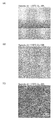
- FIGS. 1A to 1C are diagrams illustrating a cross-sectional TEM image and a cross-sectional HR-TEM image of a metal oxide film.
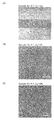
- FIGS. 2A to 2C are diagrams illustrating a cross-sectional TEM image and a cross-sectional HR-TEM image of a metal oxide film.
- 3A to 3C are diagrams illustrating a cross-sectional TEM image and a cross-sectional HR-TEM image of a metal oxide film.
- FIGS. 4A to 4C are diagrams illustrating an XRD measurement result and an electron beam diffraction pattern of a metal oxide film.
- FIGS. 5A to 5C FIGS.
- FIGS. 5A to 5C are diagrams illustrating an XRD measurement result and an electron diffraction pattern of a metal oxide film.
- FIGS. 7A and 7B are diagrams for explaining electron diffraction patterns.
- FIG. 8 is a diagram for explaining a line profile of an electron beam diffraction pattern.
- FIG. 9 is a conceptual diagram illustrating a line profile of an electron beam diffraction pattern, a relative luminance R of the line profile, and a half width of a spectrum.
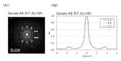
- FIGS. 10A1, 10A2, 10B1, and 10B2 A diagram illustrating an electron beam diffraction pattern and a luminance profile.
- FIG. 11A1 and 11A2 A diagram illustrating an electron diffraction pattern and a luminance profile.
- FIG. 12 is a diagram for explaining relative luminance estimated from an electron beam diffraction pattern of a metal oxide film.
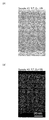
- FIGS. 13A and 13B are diagrams illustrating a cross-sectional TEM image of a metal oxide film and a cross-sectional TEM image after image analysis.
- 14A and 14B are diagrams illustrating a cross-sectional TEM image of a metal oxide film and a cross-sectional TEM image after image analysis.
- FIGS. 15A and 15B are diagrams illustrating a cross-sectional TEM image of a metal oxide film and a cross-sectional TEM image after image analysis.
- FIGS. 16A to 16C are diagrams illustrating SIMS measurement results of a metal oxide film.
- FIGS. [FIG. 17] A diagram illustrating Id-Vg characteristics.
- FIG. 18 A diagram illustrating Id-Vg characteristics.
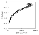
- FIG. 19 is a diagram for explaining the calculation result of the interface state density.
- FIGGS. 20A and 20B A diagram illustrating Id-Vg characteristics.
- FIG. 21 is a diagram for explaining a calculation result of defect level density.
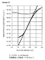
- FIG. 22 is a diagram for explaining CPM measurement results.
- FIG. 23 is a diagram for explaining the CPM measurement results.
- FIGS. 25A to 25D illustrate a mechanism for forming an oxide semiconductor film.
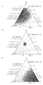
- FIGS. 26A to 26C each illustrate a range of the atomic ratio of an oxide semiconductor film.
- FIG. 27 illustrates a crystal of InMZnO 4 .
- FIG 28 illustrates an energy band in a transistor in which an oxide semiconductor film is used for a channel region.
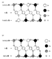
- FIGS. 29A and 29B A diagram illustrating the structure of a nanocluster.
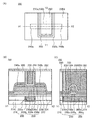
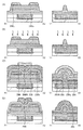
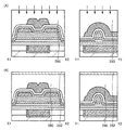
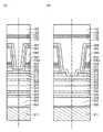
- FIGS. 30A to 30C are diagrams illustrating a top view and a cross-sectional structure of a transistor according to an embodiment. [FIG. 31A thru
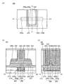
- FIGS. 32A to 32C are diagrams illustrating a top view and a cross-sectional structure of a transistor according to an embodiment.
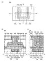
- FIGS. 33A to 33C Top views and cross-sectional views of a transistor according to an embodiment.
- FIGS. 34A to 34C A diagram illustrating a top view and a cross-sectional structure of a transistor according to an embodiment.
- FIGS. 35A to 35C A diagram illustrating a top view and a cross-sectional structure of a transistor according to an embodiment.
- FIGS. 36A to 36C are diagrams illustrating a top view and a cross-sectional structure of a transistor according to an embodiment.
- FIGS. 36A to 36C are diagrams illustrating a top view and a cross-sectional structure of a transistor according to an embodiment.
- FIGS. 37A to 37C are diagrams illustrating a top view and a cross-sectional structure of a transistor according to an embodiment.
- FIGS. 38A to 38C are diagrams illustrating a top view and a cross-sectional structure of a transistor according to an embodiment.
- FIGS. 39A to 39E illustrate an example of a method for manufacturing a transistor according to Embodiment.
- FIGS. 40A to 40D illustrate a method for manufacturing a transistor according to Embodiment.
- FIGS. FIGS. 41A to 41D illustrate a method for manufacturing a transistor according to Embodiment.
- FIGS. 42A and 42B are diagrams illustrating an example of a method for manufacturing a transistor according to Embodiment. [FIGS.
- FIG. 43A and 43B A circuit diagram of a semiconductor device according to an embodiment.
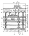
- FIG. 44 illustrates a cross-sectional structure of a semiconductor device according to an embodiment.
- FIG. 45 illustrates a cross-sectional structure of a semiconductor device according to an embodiment.
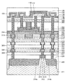
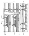
- FIG. 46 illustrates a cross-sectional structure of a semiconductor device according to an embodiment.
- FIG. 47 illustrates a cross-sectional structure of a semiconductor device according to an embodiment.
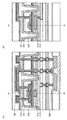
- 48A and 48B are diagrams illustrating a cross-sectional structure of a semiconductor device according to an embodiment.
- FIGS. 49A and 49B are views illustrating a cross-sectional structure of a semiconductor device according to an embodiment.
- FIGS. 49A and 49B are views illustrating a cross-sectional structure of a semiconductor device according to an embodiment.
- FIGS. 50A and 50B are diagrams illustrating a cross-sectional structure of a semiconductor device according to an embodiment.
- FIG. 51 illustrates a cross-sectional structure of a semiconductor device according to an embodiment.
- FIGS. 52A and 52B are diagrams illustrating a circuit diagram and a cross-sectional structure of a semiconductor device according to an embodiment.
- FIG. 53 illustrates a cross-sectional structure of a semiconductor device according to an embodiment.
- FIG. 54 is a circuit diagram illustrating a memory device according to one embodiment of the present invention.
- FIG. 55 is a circuit diagram illustrating a memory device according to one embodiment of the present invention.
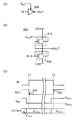
- FIGGS. 56A to 56C A circuit diagram and a timing chart illustrating one embodiment of the present invention. [FIGS.
- FIGS. 62A and 62B are circuit diagrams illustrating one embodiment of the present invention.
- FIGS. 62A and 62B are circuit diagrams illustrating one embodiment of the present invention.
- FIGS. 64A and 64B are circuit diagrams for illustrating one embodiment of the present invention.
- FIGS. 65A to 65C are circuit diagrams illustrating one embodiment of the present invention.
- FIGS. 66A and 66B are circuit diagrams illustrating one embodiment of the present invention.
- FIG. 67 is a block diagram illustrating a semiconductor device according to one embodiment of the present invention.
- FIG. 68 is a circuit diagram illustrating a semiconductor device according to one embodiment of the present invention.
- FIGS. 69A and 69B are top views illustrating a semiconductor device according to one embodiment of the present invention.
- FIGS. 70A and 70B are block diagrams illustrating a semiconductor device according to one embodiment of the present invention.
- FIGS. 70A and 70B are block diagrams illustrating a semiconductor device according to one embodiment of the present invention.
- FIG. 71A and 71B are cross-sectional views illustrating a semiconductor device according to one embodiment of the present invention.
- FIG. 72 is a cross-sectional view illustrating a semiconductor device according to one embodiment of the present invention.
- FIGS. 73A and 73B are top views illustrating a semiconductor device according to one embodiment of the present invention.
- FIGS. 74A and 74B are a flow chart for explaining one embodiment of the present invention and a perspective view showing a semiconductor device.
- FIGS. 75A to 75F are perspective views illustrating electronic devices according to one embodiment of the present invention.
- FIG. 76 is a diagram for explaining the measurement results of the XRD spectrum of a sample. [FIG. 77A thru
- a transistor is an element having at least three terminals including a gate, a drain, and a source.
- a channel region is provided between the drain (drain terminal, drain region or drain electrode) and the source (source terminal, source region or source electrode), and a current flows through the drain, channel region, and source. It is something that can be done.
- a channel region refers to a region through which a current mainly flows.
- the functions of the source and drain may be switched when transistors with different polarities are used or when the direction of current changes during circuit operation. Therefore, in this specification and the like, the terms source and drain can be used interchangeably.
- “electrically connected” includes a case of being connected via “something having an electric action”.
- the “thing having some electric action” is not particularly limited as long as it can exchange electric signals between connection targets.
- “thing having some electric action” includes electrodes, wiring, switching elements such as transistors, resistance elements, inductors, capacitors, and other elements having various functions.
- parallel means a state in which two straight lines are arranged at an angle of ⁇ 10 ° to 10 °. Therefore, the case of ⁇ 5 ° to 5 ° is also included.
- Very refers to a state in which two straight lines are arranged at an angle of 80 ° to 100 °. Therefore, the case of 85 ° to 95 ° is also included.
- film and “layer” can be interchanged.
- conductive layer may be changed to the term “conductive film”.
- insulating film may be changed to the term “insulating layer” in some cases.
- off-state current refers to drain current when a transistor is off (also referred to as a non-conduction state or a cutoff state).
- the off state is a state where the voltage Vgs between the gate and the source is lower than the threshold voltage Vth in the n-channel transistor, and the voltage Vgs between the gate and the source in the p-channel transistor unless otherwise specified. Is higher than the threshold voltage Vth.
- the off-state current of an n-channel transistor sometimes refers to a drain current when the voltage Vgs between the gate and the source is lower than the threshold voltage Vth.
- the transistor off current may depend on Vgs. Therefore, the off-state current of the transistor being I or less sometimes means that there exists a value of Vgs at which the off-state current of the transistor is I or less.
- the off-state current of a transistor may refer to an off-state current in an off state at a predetermined Vgs, an off state in a Vgs within a predetermined range, or an off state in Vgs at which a sufficiently reduced off current is obtained.
- the drain current when Vgs is 0.5 V is 1 ⁇ 10 ⁇ 9 A
- the drain current when Vgs is 0.1 V is 1 ⁇ 10 ⁇ 13 A.
- the n-channel transistor has a drain current of 1 ⁇ 10 ⁇ 19 A when Vgs is ⁇ 0.5 V and a drain current of 1 ⁇ 10 ⁇ 22 A when Vgs is ⁇ 0.8 V. Since the drain current of the transistor is 1 ⁇ 10 ⁇ 19 A or less when Vgs is ⁇ 0.5 V or Vgs is in the range of ⁇ 0.5 V to ⁇ 0.8 V, the off-state current of the transistor is 1 It may be said that it is below x10 ⁇ -19> A. Since there is Vgs at which the drain current of the transistor is 1 ⁇ 10 ⁇ 22 A or less, the off-state current of the transistor may be 1 ⁇ 10 ⁇ 22 A or less.
- the off-state current of a transistor having a channel width W may be represented by a current value flowing around the channel width W.
- the current value flows around a predetermined channel width (for example, 1 ⁇ m).
- the unit of off-current may be represented by a unit having a dimension of current / length (for example, A / ⁇ m).
- Transistor off-state current may depend on temperature.
- off-state current may represent off-state current at room temperature, 60 ° C., 85 ° C., 95 ° C., or 125 ° C. unless otherwise specified.
- off-state current at a temperature at which reliability of the semiconductor device including the transistor is guaranteed, or temperature at which the semiconductor device including the transistor is used for example, a temperature in the range of 5 ° C. to 35 ° C.).
- the off-state current of a transistor is I or less means that room temperature, 60 ° C., 85 ° C., 95 ° C., 125 ° C., a temperature at which the reliability of the semiconductor device including the transistor is guaranteed, or the transistor is included. There may be a case where there is a value of Vgs at which the off-state current of the transistor is equal to or lower than I at a temperature at which a semiconductor device or the like is used (for example, a temperature in a range of 5 ° C. to 35 ° C.).
- the off-state current of the transistor may depend on the voltage Vds between the drain and the source.
- the off-state current is Vds of 0.1V, 0.8V, 1V, 1.2V, 1.8V, 2.5V, 3V, 3.3V, 10V, 12V, 16V unless otherwise specified. Or an off-current at 20V.
- Vds in which reliability of a semiconductor device or the like including the transistor is guaranteed, or an off-current in Vds used in the semiconductor device or the like including the transistor may be represented.
- the off-state current of the transistor is equal to or less than I.
- Vds is 0.1V, 0.8V, 1V, 1.2V, 1.8V, 2.5V, 3.3V, 3.3V, 3.3V, 10V, 12V, 16V, 20V.
- Vgs at which the off-state current of the transistor is less than or equal to Vds at which Vds guarantees the reliability of the semiconductor device including the transistor or Vds used in the semiconductor device or the like including the transistor. May be pointed to.
- the drain may be read as the source. That is, the off-state current sometimes refers to a current that flows through the source when the transistor is off.
- off-state current may refer to current that flows between a source and a drain when a transistor is off, for example.
- the threshold voltage of a transistor refers to a gate voltage (Vg) when a channel is formed in the transistor.
- the threshold voltage of a transistor is a maximum slope in a curve (Vg- ⁇ Id characteristic) in which the gate voltage (Vg) is plotted on the horizontal axis and the square root of the drain current (Id) is plotted on the vertical axis.
- Vg- ⁇ Id characteristic a curve in which the gate voltage (Vg) is plotted on the horizontal axis and the square root of the drain current (Id) is plotted on the vertical axis.
- a gate voltage (Vg) at the intersection of a straight line obtained by extrapolating a certain tangent and the square root of the drain current (Id) is 0 (Id is 0 A) may be indicated.
- the threshold voltage of the transistor is a gate in which the channel length is L, the channel width is W, and the value of Id [A] ⁇ L [ ⁇ m] / W [ ⁇ m] is 1 ⁇ 10 ⁇ 9 [A]. It may refer to voltage (Vg).
- the voltage often indicates a potential difference between a certain potential and a reference potential (for example, a ground potential (GND) or a source potential).
- a voltage can be rephrased as a potential.
- the potential (voltage) is relative and is determined by a relative magnitude from a reference potential. Therefore, even when “ground potential” is described, the potential is not always 0V.
- the lowest potential in the circuit may be the “ground potential”.
- an intermediate potential in the circuit may be a “ground potential”. In that case, a positive potential and a negative potential are defined based on the potential.
- the channel length refers to, for example, a region where a semiconductor (or a portion where current flows in the semiconductor when the transistor is on) and a gate electrode overlap with each other in a top view of the transistor, or a region where a channel is formed
- the channel length is not necessarily the same in all regions. That is, the channel length of one transistor may not be fixed to one value. Therefore, in this specification, the channel length is any one of values, the maximum value, the minimum value, or the average value in a region where a channel is formed.
- the channel width is, for example, a region in which a semiconductor (or a portion in which a current flows in the semiconductor when the transistor is on) and a gate electrode overlap each other, or a source and a drain in a region where a channel is formed. This is the length of the part. Note that in one transistor, the channel width is not necessarily the same in all regions. That is, the channel width of one transistor may not be fixed to one value. Therefore, in this specification, the channel width is any one of values, the maximum value, the minimum value, or the average value in a region where a channel is formed.
- the channel width in a region where a channel is actually formed (hereinafter referred to as an effective channel width) and the channel width shown in a top view of the transistor (hereinafter, apparent channel width). May be different).
- the effective channel width is larger than the apparent channel width shown in the top view of the transistor, and the influence may not be negligible.
- the ratio of the channel region formed on the side surface of the semiconductor may be large. In that case, the effective channel width in which the channel is actually formed is larger than the apparent channel width shown in the top view.
- an apparent channel width which is a length of a portion where a source and a drain face each other in a region where a semiconductor and a gate electrode overlap with each other is expressed as “enclosed channel width ( SCW: Surrounded Channel Width).
- SCW Surrounded Channel Width
- channel width in the case where the term “channel width” is simply used, it may denote an enclosed channel width or an apparent channel width.
- channel width in the case where the term “channel width” is simply used, it may denote an effective channel width. Note that the channel length, channel width, effective channel width, apparent channel width, enclosed channel width, and the like can be determined by obtaining a cross-sectional TEM image and analyzing the image. it can.
- the calculation may be performed using the enclosed channel width. In that case, the value may be different from that calculated using the effective channel width.
- the “semiconductor” in this specification and the like can be called an “insulator” in some cases.
- an “insulator” in this specification and the like can be called a “semiconductor” in some cases.
- the “insulator” in this specification and the like can be referred to as a “semi-insulator” in some cases.
- the semiconductor device may have characteristics as a “conductor”. Further, the boundary between the “semiconductor” and the “conductor” is ambiguous, and there are cases where it cannot be strictly distinguished. Therefore, a “semiconductor” in this specification and the like can be called a “conductor” in some cases. Similarly, a “conductor” in this specification and the like can be called a “semiconductor” in some cases.
- a semiconductor impurity refers to an element other than a main component constituting a semiconductor film.
- an element having a concentration of less than 0.1 atomic% is an impurity.
- DOS Density of State
- examples of impurities that change the characteristics of the semiconductor include a Group 1 element, a Group 2 element, a Group 13 element, a Group 14 element, a Group 15 element, and components other than the main component.
- Transition metals and the like in particular, hydrogen (also included in water), lithium, sodium, silicon, boron, phosphorus, carbon, nitrogen, and the like.
- oxygen vacancies may be formed by mixing impurities such as hydrogen, for example.
- impurities that change the characteristics of the semiconductor include Group 1 elements, Group 2 elements, Group 13 elements, and Group 15 elements other than oxygen and hydrogen.
- oxide when it is simply described as an oxide, it can be read as a metal oxide, an oxide semiconductor, an oxide insulator, or an oxide conductor.
- One embodiment of the present invention is a metal oxide film including two kinds of crystal parts.
- One of the crystal parts also referred to as the first crystal part
- has orientation in the thickness direction of the film also referred to as a film surface direction, a film formation surface, or a direction perpendicular to the film surface
- c It is a crystal part having axial orientation.
- Another of the crystal parts (also referred to as a second crystal part) is a crystal part that does not have c-axis orientation and is oriented in various directions.
- the metal oxide film of one embodiment of the present invention includes such two kinds of crystal parts.
- the crystal part having c-axis orientation is described separately from the first crystal part, and the crystal part not having c-axis orientation is described separately from the second crystal part.
- these may not be distinguished because there is no difference in crystallinity and crystal size. That is, the metal oxide film of one embodiment of the present invention can be expressed without distinction.
- the metal oxide film of one embodiment of the present invention includes a plurality of crystal parts, and at least one of the crystal parts in the film may have c-axis orientation. Further, among the crystal parts present in the film, the ratio of the crystal parts not having c-axis orientation may be larger than the ratio of the crystal parts having c-axis orientation.
- a plurality of crystal parts are observed in an observation image with a transmission electron microscope in a cross-section in the film thickness direction, and the c-axis orientation among the plurality of crystal parts.
- the second crystal part having no property is observed more than the first crystal part having the c-axis orientation.
- the metal oxide film of one embodiment of the present invention has a large proportion of the second crystal part which does not have c-axis orientation.
- the following excellent effects can be obtained by increasing the ratio of the second crystal part having no c-axis orientation in the metal oxide film.
- the second crystal part having no c-axis orientation can be an oxygen diffusion path. Therefore, when there is a sufficient oxygen supply source in the vicinity of the metal oxide film, oxygen is supplied to the first crystal part having c-axis orientation through the second crystal part having no c-axis orientation. Can be supplied. Therefore, the amount of oxygen vacancies in the metal oxide film can be reduced.
- the second crystal part having no c-axis orientation serves as an oxygen diffusion path, and oxygen can be supplied to the first crystal part having the c-axis orientation.
- a metal oxide film including a first crystal part having a second crystal part and a second crystal part having no c-axis orientation is referred to as an oxygen-deficient metal oxide film or an oxygen-deficient oxide semiconductor film. There is a case.
- the specific crystal plane has orientation with respect to the thickness direction of the film. Therefore, when X-ray diffraction (XRD) measurement is performed on the metal oxide film including the first crystal part in a direction substantially perpendicular to the upper surface of the film, the first diffraction crystal is obtained at a predetermined diffraction angle (2 ⁇ ). A diffraction peak derived from the crystal part 1 is confirmed. On the other hand, even if the metal oxide film has the first crystal part, a diffraction peak may not be sufficiently confirmed due to scattering of X-rays by the support substrate or an increase in background. Note that the height (intensity) of the diffraction peak increases in accordance with the presence ratio of the first crystal portion included in the metal oxide film, and can be an index for estimating the crystallinity of the metal oxide film.
- XRD X-ray diffraction
- electron diffraction is one method for evaluating the crystallinity of a metal oxide film. For example, when an electron beam diffraction measurement is performed on a cross section and an electron beam diffraction pattern of the metal oxide film of one embodiment of the present invention is observed, the first region having a diffraction spot due to the first crystal portion, And a second region having a diffraction spot due to the two crystal parts.
- the first region having a diffraction spot due to the first crystal part is derived from the crystal part having c-axis orientation.
- the second region having a diffraction spot due to the second crystal part is derived from a crystal part having no orientation or a crystal part that is disorderly oriented in any direction. Therefore, different patterns may be observed depending on the beam diameter of the electron beam used for electron beam diffraction, that is, the area of the region to be observed.
- electron beam diffraction in which the beam diameter of an electron beam is measured from 1 nm ⁇ to 100 nm ⁇ is referred to as nano beam electron diffraction (NBED: Nano Beam Electron Diffraction).
- the crystallinity of the metal oxide film of one embodiment of the present invention may be evaluated by a method different from that of NBED.
- the method for evaluating the crystallinity of the metal oxide film include electron diffraction, X-ray diffraction, and neutron diffraction.
- electron diffractions in addition to the NBED shown above, transmission electron microscope (TEM: Transmission Electron Microscopy), scanning electron microscope (SEM: Scanning Electron Microscopy), convergent electron diffraction (CBED: Convergent Electron Limit) Field electron diffraction (SAED: Selected Area Electron Diffraction) or the like can be suitably used.
- a ring-shaped pattern is observed in the nanobeam electron diffraction pattern under the condition that the beam diameter of the electron beam is increased (for example, 25 nm ⁇ to 100 nm ⁇ or 50 nm ⁇ to 100 nm ⁇ ).
- the ring-shaped pattern may have a luminance distribution in the radial direction.
- in NBED in an electron beam diffraction pattern under a condition that the beam diameter of the electron beam is sufficiently small (for example, 1 nm ⁇ to 10 nm ⁇ ), distribution is performed in the circumferential direction (also referred to as ⁇ direction) at the position of the ring-shaped pattern. Multiple spots may be observed. That is, a ring-shaped pattern that can be seen under the condition that the beam diameter of the electron beam is increased is formed by an aggregate of the plurality of spots.
- Sample A1 is a sample in which a metal oxide film having a thickness of about 100 nm is formed on a glass substrate.
- the metal oxide film includes indium, gallium, and zinc.
- the ratio of the oxygen flow rate to the total gas flow rate described above may be referred to as an oxygen flow rate ratio. Note that the oxygen flow rate ratio in the production conditions of the sample A1 is 30%.
- Sample A2 is a sample in which a metal oxide film having a thickness of about 100 nm is formed on a glass substrate.
- the substrate was heated to 130 ° C., and argon gas having a flow rate of 180 sccm and oxygen gas having a flow rate of 20 sccm were introduced into the chamber of the sputtering apparatus.
- the oxygen flow rate ratio under the production conditions of sample A2 is 10%.
- the conditions other than the substrate temperature and the oxygen flow rate ratio were the same as those of the sample A1 described above.
- Sample A3 is a sample in which a metal oxide film having a thickness of about 100 nm is formed on a glass substrate.
- the substrate was set to room temperature (for example, 20 ° C. to 30 ° C., and the room temperature is described as RT in Table 1), argon gas with a flow rate of 180 sccm, 20 sccm of oxygen gas was introduced into the chamber of the sputtering apparatus.
- the oxygen flow rate ratio under the production conditions of sample A3 is 10%.
- the conditions other than the substrate temperature and the oxygen flow rate ratio were the same as those of the sample A1 described above.
- Table 1 shows the manufacturing conditions of Samples A1 to A3.
- FIGS. 1A to 3C show the results of cross-sectional TEM observation of samples A1 to A3.
- 1A and 1B are cross-sectional TEM images of the sample A1
- FIGS. 2A and 2B are cross-sectional TEM images of the sample A2
- FIGS. 3A and 3B are cross-sectional TEM images of the sample A3.
- FIG. 1C is a high-resolution transmission electron microscope (HR-TEM) image of the cross section of the sample A1
- FIG. 2C is a cross-sectional HR-TEM image of the sample A2
- FIG. 3C is the sample A3. It is a cross-sectional HR-TEM image.
- a spherical aberration correction function may be used for observation of the cross-sectional HR-TEM image.
- a high-resolution TEM image using the spherical aberration correction function is particularly referred to as a Cs-corrected high-resolution TEM image.
- the Cs-corrected high resolution TEM image can be observed, for example, with an atomic resolution analytical electron microscope JEM-ARM200F manufactured by JEOL Ltd.
- FIG. 4A shows the XRD measurement result of sample A1
- FIG. 5A shows the XRD measurement result of sample A2
- FIG. 6A shows the XRD measurement result of sample A3.
- a powder method (also referred to as a ⁇ -2 ⁇ method), which is a kind of out-of-plane method, was used.
- the ⁇ -2 ⁇ method is a method of measuring the X-ray diffraction intensity by changing the incident angle of the X-ray and setting the angle of the detector provided facing the X-ray source to be the same as the incident angle.
- GIXRD Gram-Incidence XRD
- GIXRD is a kind of out-of-plane method in which X-rays are incident from the film surface at an angle of about 0.40 ° and the X-ray diffraction intensity is measured by changing the angle of the detector.
- Method also referred to as a thin film method or a Seemann-Bohlin method
- 4A, 5A, and 6A the vertical axis indicates the diffraction intensity in arbitrary units
- the horizontal axis indicates the angle 2 ⁇ .
- the thickness of the sample in the depth direction is, for example, 10 nm to 100 nm, typically 10 nm to 50 nm.
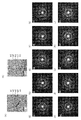
- FIGS. 4B and 4C show the electron diffraction pattern of sample A1
- FIGS. 5B and 5C show the electron diffraction pattern of sample A2
- FIGS. 6B and 6C show the electron diffraction pattern of sample A3, respectively.
- the electron beam diffraction patterns shown in FIGS. 4B and 4C, FIGS. 5B and 5C, and FIGS. 6B and 6C are image data in which the contrast is adjusted so that the electron beam diffraction patterns are clear. 4B and 4C, FIGS. 5B and 5C, and FIGS. 6B and 6C, the brightest bright spot at the center is due to the incident electron beam, and the center of the electron diffraction pattern (both direct spot or transmitted wave). Say).
- FIG. 4B when the beam diameter of the incident electron beam is 1 nm ⁇ , a plurality of spots distributed in a circumferential shape are seen, so that the metal oxide film is extremely minute and has a plane orientation. It can be seen that a plurality of crystal parts oriented in all directions are mixed.
- FIG. 4C when the beam diameter of the incident electron beam is 100 nm ⁇ , the diffraction spots from the plurality of crystal parts are connected, and the luminance is averaged to form a ring-shaped diffraction pattern. I can confirm. In FIG. 4C, two ring-shaped diffraction patterns having different radii can be observed.
- the first ring and the second ring are referred to from the diffraction pattern having a small diameter. It can be confirmed that the brightness of the first ring is higher than that of the second ring. In addition, two spots (first areas) with high luminance are confirmed at positions overlapping the first ring.
- the radial distance from the center of the first ring substantially coincides with the radial distance from the center of the diffraction spot on the (009) plane in the structural model of single crystal InGaZnO 4 . Further, the first region is a diffraction spot due to the c-axis orientation.
- the crystal part (hereinafter referred to as “c-axis orientation” which is oriented in any direction is included in the metal oxide film. It can also be said that there is a crystal part or a second crystal part).
- the two first regions are arranged symmetrically with respect to the center point of the electron beam diffraction pattern and have the same luminance, it is presumed that the two first regions have a two-fold symmetry.
- the direction of the straight line connecting the two first regions and the center is the direction of the c-axis of the crystal part. Match.
- the vertical direction is the film thickness direction, it can be seen that there is a crystal part in which the c-axis is oriented in the film thickness direction in the metal oxide film.
- the metal oxide film of the sample A1 is a film in which a crystal part having c-axis orientation and a crystal part not having c-axis orientation are mixed.
- the electron diffraction patterns shown in FIGS. 5B and 5C and FIGS. 6B and 6C are almost the same as the electron diffraction patterns shown in FIGS. 4B and 4C.
- the brightness of the two spots (first region) due to the c-axis orientation is the brightest in the sample A1, darker in the order of the sample A2 and the sample A3, and the proportion of crystal parts having c-axis orientation.
- sample A1 is the highest, and decreases in the order of sample A2 and sample A3.
- FIG. 7A is an electron beam diffraction pattern measured at a beam diameter of 100 nm with respect to a metal oxide film having a thickness of 100 nm
- FIG. 7B is a graph obtained by adjusting the contrast of the electron beam diffraction pattern shown in FIG. 7A. It is the obtained electron beam diffraction pattern.
- first regions two clear spots (first regions) are observed above and below the direct spot. These two spots (first regions) are caused by diffraction spots corresponding to the (001) plane in the structural model of InGaZnO 4 , that is, crystal parts having c-axis orientation.
- a ring-like pattern (second region) with low luminance appears to overlap with the first region approximately concentrically. This is because the spot due to the structure of the crystal part (second crystal part) having no c-axis orientation is averaged and formed into a ring shape by setting the electron beam diameter to 100 nm.
- the crystallinity of the metal oxide film can be quantified by acquiring and comparing the line profile including the first region and the line profile including the second region.
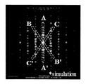
- FIG. 8 shows a region AA ′, a region BB ′, and a region CC ′ in a simulation pattern of electron beam diffraction obtained when the (100) plane of the structural model of InGaZnO 4 is irradiated with an electron beam. It is the figure which attached the auxiliary line of.
- the region A-A ′ shown in FIG. 8 includes a straight line passing through two diffraction spots caused by the first crystal part having c-axis orientation and a direct spot. Further, the region BB ′ and the region CC ′ shown in FIG. 8 each include a straight line passing through a region where a diffraction spot due to the first crystal part having c-axis orientation is not observed and a direct spot. .
- the angle at which the region AA ′ and the region BB ′ or the region CC ′ intersect is around 34 °, specifically, 30 ° to 38 °, preferably 32 ° to 36 °, More preferably, the angle may be not less than 33 ° and not more than 35 °.
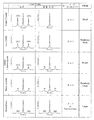
- FIG. 9 is a diagram illustrating an image of a line profile for each structure, a relative luminance R, and a half width of a spectrum (FWHM: Full Width at Half Maximum) resulting from the c-axis orientation obtained from the electron diffraction pattern. .
- the relative luminance R shown in FIG. 9 is a value obtained by dividing the integrated luminance intensity in the region AA ′ by the integrated luminance intensity in the region BB ′ or the integrated luminance intensity in the region CC ′. is there.
- the integrated intensity of luminance in the areas AA ′, BB ′, and CC ′ is obtained by removing the direct spot appearing at the center position and the background caused by the direct spot. It is.
- the strength of the c-axis orientation can be defined quantitatively.
- the peak intensity of the diffraction spot due to the first crystal part having the c-axis orientation in the region AA ′ is high, and the region BB Since the diffraction spot due to the first crystal part having the c-axis orientation is not seen in 'and the region CC', the relative luminance R exceeds 1 and becomes extremely large.
- the relative luminance R is highest in the single crystal metal oxide film, and decreases in the order of CAAC + nanocrystal, nanocrystal, and amorphous metal oxide film only in CAAC (details of CAAC will be described later).
- the relative luminance R is 1 in a nanocrystal and amorphous metal oxide film having no specific orientation.
- the full width at half maximum of the single crystal metal oxide film is the smallest, the full width at half maximum increases in the order of CAAC only, CAAC + nanocrystal, and nanocrystal metal oxide film.
- the full width at half maximum is extremely large. It becomes a profile called halo.
- the intensity ratio of the integrated intensity of luminance in the first region to the integrated intensity of luminance in the second region is important information in terms of estimating the existence ratio of crystal parts having orientation.
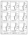
- FIGS. 10A1 and 10A2 The analysis results using the line profile of sample A1 are shown in FIGS. 10A1 and 10A2, the analysis results using the line profile of sample A2 are shown in FIGS. 10B1 and 10B2, and the analysis results using the line profile of sample A3 are shown in FIGS. 11A1 and 11A2. , Respectively.
- FIG. 10A1 is an electron beam diffraction pattern in which the region AA ′, the region BB ′, and the region CC ′ are described in the electron beam diffraction pattern illustrated in FIG. 4C.
- FIG. 10B1 is illustrated in FIG. 11A1 is an electron beam diffraction pattern in which a region AA ′, a region BB ′, and a region CC ′ are described in the electron beam diffraction pattern shown.
- FIG. 11A1 shows a region A ⁇ in the electron beam diffraction pattern shown in FIG. It is the electron beam diffraction pattern which described A ', area
- the area A-A ′, the area B-B ′, and the area C-C ′ can be obtained by normalizing with the brightness of the direct spot appearing at the center position of the electron diffraction pattern. This also allows a relative comparison between the samples.
- the background luminance may be calculated by linear approximation. For example, a region located on the lower luminance side than a straight line drawn along the skirts on both sides of the target peak can be subtracted as the background.
- the integrated intensity of luminance in the region A-A ′, the region B-B ′, and the region C-C ′ was calculated from the data obtained by subtracting the background by the above-described method.
- a value obtained by dividing the integrated luminance intensity in the region A-A ′ by the integrated luminance intensity in the region B-B ′ or the integrated luminance intensity in the region C-C ′ was obtained as the relative luminance R.
- FIG. 12 shows the relative luminance R of the samples A1 to A3.
- the integrated intensity of the luminance in the region AA ′ is the luminance in the region BB ′ at the peaks located on the left and right of the direct spot in the luminance profiles shown in FIGS. 10A2, 10B2, and 11A2.
- the relative luminance R of the samples A1 to A3 is as shown below.
- -Relative luminance R of sample A1 25.00
- -Relative luminance R of the sample A2 3.04
- -Relative luminance R of sample A3 1.05
- the above-mentioned relative luminance R is an average value at four positions.
- the relative luminance R is highest in the sample A1, and decreases in the order of the sample A2 and the sample A3.
- the relative luminance R is more than 1 and 40 or less, preferably more than 1 and 10 or less, more preferably 1 It is preferable to use a metal oxide film that exceeds 3 and is 3 or less.
- Presence ratio of crystal part The existence ratio of the crystal part in the metal oxide film can be estimated by analyzing the cross-sectional TEM image.
- a two-dimensional fast Fourier transform (FFT: Fast Fourier Transform) process is performed on a TEM image captured at a high resolution to obtain an FFT image.
- FFT Fast Fourier Transform
- the obtained FFT image is subjected to a mask process that leaves a range having periodicity and removes the rest.
- the masked FFT image is then subjected to a two-dimensional inverse Fourier transform (IFFT: Inverse Fast Fourier Transform) to obtain an FFT filtered image.
- IFFT Inverse Fast Fourier Transform
- the existence ratio of the crystal part can be estimated from the ratio of the area of the remaining image. Further, by subtracting the area of the remaining image from the area of the region used for the calculation (also referred to as the area of the original image), it is possible to estimate the existence ratio of the portion other than the crystal part.
- FIG. 13A shows a cross-sectional TEM image of sample A1
- FIG. 13B shows an image obtained after image analysis of the cross-sectional TEM image of sample A1.
- 14A shows a cross-sectional TEM image of sample A2
- FIG. 14B shows an image obtained after image analysis of the cross-sectional TEM image of sample A2.
- FIG. 15A shows a cross-sectional TEM image of sample A3, and FIG. 15B shows an image obtained after image analysis of the cross-sectional TEM image of sample A3.
- the white area in the metal oxide film corresponds to the area including the crystal part having orientation, and the black area does not have orientation. This corresponds to a crystal part or a region including a crystal part oriented in various directions.
- the ratio of the area excluding the region including the crystal part having orientation in the sample A1 was about 43.1%.
- the ratio of the portion excluding the region including the crystal portion having orientation in the sample A2 was about 61.7%.
- the ratio of the portion excluding the region including the crystal part having orientation in the sample A3 is about 89.5%.
- the metal oxide film is a film having extremely high crystallinity. It is preferable because oxygen vacancies are difficult to make and electrical characteristics are very stable.
- the ratio of the portion excluding the crystal part having orientation in the metal oxide film is 40% or more and less than 100%, preferably 60% or more and 90% or less, the metal oxide film has orientation.
- the crystal part which has and the crystal part which does not have orientation coexist in a moderate ratio, and it can make electrical characteristics stable and high mobility compatible.
- LGBR Lateral Growth Buffer Region
- samples B1 to B3 were produced.
- a metal oxide film having a thickness of about 50 nm was formed on a glass substrate by a method similar to that of the sample A1 described above. Subsequently, a silicon oxynitride film having a thickness of about 30 nm, a silicon oxynitride film having a thickness of about 100 nm, and a silicon oxynitride film having a thickness of about 20 nm are stacked over the metal oxide film by a plasma CVD method.
- a metal oxide film may be described as OS and a silicon oxynitride film may be described as GI.
- an In—Sn—Si oxide film having a thickness of 5 nm was formed by a sputtering method.
- oxygen addition treatment was performed on the silicon oxynitride film.
- oxygen addition conditions using an ashing apparatus, a substrate temperature of 40 ° C., and an oxygen gas (16 O) of the flow rate 150 sccm, and a flow rate 100sccm oxygen gas (18 O) is introduced into the chamber, 15 Pa pressure Then, RF power of 4500 W was supplied for 600 seconds between parallel plate electrodes installed in the ashing device so that a bias was applied to the substrate side. Note that oxygen gas ( 16 O) was contained in the silicon oxynitride film at a main component level, and thus oxygen gas ( 18 O) was used to accurately measure the oxygen added by the oxygen addition treatment. .
- a silicon nitride film having a thickness of about 100 nm was formed by a plasma CVD method.
- Sample B2 is a sample manufactured by changing the film formation conditions of the metal oxide film from Sample B1.
- a metal oxide film having a thickness of about 50 nm was formed by a method similar to that for Sample A2 described above.
- Sample B3 is a sample manufactured by making the film formation conditions of the metal oxide film different from those of Sample B1.
- a metal oxide film with a thickness of about 50 nm was formed by a method similar to that for Sample A3 described above.
- Samples B1 to B3 were prepared by the above process.
- SIMS analysis For samples B1 to B3, the concentration of 18 O was measured by SIMS (Secondary Ion Mass Spectrometry) analysis. Note that in SIMS analysis, the above-prepared samples B1 to B3 were not subjected to heat treatment, the samples B1 to B3 were subjected to heat treatment at 350 ° C. for 1 hour in a nitrogen atmosphere, and the samples B1 to B3 were subjected to nitrogen treatment. Three conditions were set: a condition of performing heat treatment at 450 ° C. for one hour in an atmosphere.
- FIGS. 16A to 16C show the SIMS measurement results.
- 16A to 16C show the analysis results of the region including GI and OS.
- 16A to 16C show the results of analysis from the substrate side (also referred to as SSDP (Substrate Side Depth Profile) -SIMS).
- substrate side also referred to as SSDP (Substrate Side Depth Profile) -SIMS.
- the gray broken line is a profile under conditions where heat treatment is not performed
- the black broken line is a profile under conditions where heat treatment is performed at 350 ° C.
- the black solid line is subjected to heat treatment at 450 ° C. It is a profile of the condition.
- a metal oxide film in which a crystal part having orientation and a crystal part not having orientation are mixed and the ratio of the crystal part having orientation is low is a film that easily transmits oxygen, in other words, It can be confirmed that the film easily diffuses oxygen. Further, it can be confirmed that oxygen in the GI film diffuses into the OS by performing heat treatment at 350 ° C. or 450 ° C.
- LGBR regions other than crystal parts
- LGBR cross-sectional observation image
- oxygen released from the oxide film diffuses in the thickness direction of the metal oxide film by LGBR. Then, oxygen can be supplied from the lateral direction to the crystal part having orientation through the LGBR. Thereby, oxygen is sufficiently distributed to the crystal part having the orientation of the metal oxide film and other regions, and oxygen vacancies in the film can be effectively reduced.
- the side surface of the crystal part having orientation Active oxygen (atomic oxygen) is bound to.
- a metal such as In, M, or Zn is bonded to the bonded active oxygen.
- the active oxygen and a metal such as In, M, or Zn are repeatedly bonded to each other so that solid phase growth occurs laterally from the side surface of the crystal part having orientation. Lateral growth of crystal parts having such orientation can also be called self-organization.
- a hydrogen atom that is not bonded to a metal atom is present in the metal oxide film, this may be bonded to an oxygen atom to form OH and be fixed. Therefore, the oxygen deficiency of the metal oxide film by depositing a low temperature fixed amount state where hydrogen atoms are trapped (referred to as V O H) to (V O) (for example, about 1 ⁇ 10 17 cm -3) By forming, OH is suppressed from being formed.
- V O H generates carriers, a certain amount of carriers are present in the metal oxide film. Thereby, a metal oxide film with an increased carrier density can be formed.
- oxygen vacancies are simultaneously formed during film formation, but the oxygen vacancies can be reduced by introducing oxygen through LGBR as described above. By such a method, a metal oxide film having a relatively high carrier density and sufficiently reduced oxygen vacancies can be formed.
- the region other than the crystal part having the orientation constitutes a very fine crystal part having no orientation at the time of film formation, no clear crystal grain boundary is observed in the metal oxide film.
- the extremely fine crystal part is located between a plurality of crystal parts having orientation.
- the fine crystal part grows in the lateral direction by heat at the time of film formation, and is bonded to an adjacent crystal part having orientation.
- the fine crystal part also functions as a region for generating carriers. Accordingly, it is considered that the field-effect mobility of the metal oxide film having such a structure can be remarkably improved by being applied to a transistor.
- oxygen permeability is improved by using a metal oxide film formed under conditions of low temperature and low oxygen flow rate. For this reason, for example, an increase in the amount of oxygen diffused during the manufacturing process of the transistor may reduce defects such as oxygen vacancies in the metal oxide film and at the interface between the metal oxide film and the insulating film. Guessed. It is suggested that the on-state current of the transistor is remarkably increased as a result of reducing the defect level density by such an effect.
- a transistor with improved on-state current can be suitably used for a switch capable of charging and discharging a capacitor at high speed.
- it can be suitably used for a demultiplexer circuit or the like.
- etching treatment in an oxygen atmosphere after forming a metal oxide film and forming an oxide insulating film such as a silicon oxide film thereon.
- Such treatment can reduce the hydrogen concentration in addition to supplying oxygen into the film.
- fluorine remaining in the chamber may be doped into the metal oxide film at the same time. Fluorine exists as a negatively charged fluorine atom, and is combined with a positively charged hydrogen atom by Coulomb force to generate HF. HF is released out of the metal oxide film during the plasma treatment, and as a result, the hydrogen concentration in the metal oxide film can be reduced.
- oxygen atoms and hydrogen may be combined and released as H 2 O out of the film.
- a configuration in which a silicon oxide film (or silicon oxynitride film) is stacked on a metal oxide film is considered. Since fluorine in the silicon oxide film is bonded to hydrogen in the film and can exist as electrically neutral HF, it does not affect the electrical characteristics of the metal oxide film. In addition, although Si-F bond may arise, this also becomes electrically neutral. Further, it is considered that HF in the silicon oxide film does not affect oxygen diffusion.
- oxygen vacancies in the metal oxide film are reduced, and hydrogen that is not bonded to metal atoms in the film is reduced, so that reliability can be improved. Further, it is considered that the electrical characteristics are improved when the carrier concentration of the metal oxide film is a certain level or more.
- Samples C1 to C3 are transistors having a channel length L of 6 ⁇ m and a channel width W of 50 ⁇ m.
- a titanium film with a thickness of 10 nm and a copper film with a thickness of 100 nm were formed on a glass substrate using a sputtering apparatus. Subsequently, the conductive film was processed by a photolithography method.
- insulating films were formed on the substrate and the conductive film.
- the insulating film was continuously formed in a vacuum using a plasma enhanced chemical vapor deposition (PECVD) apparatus.
- PECVD plasma enhanced chemical vapor deposition
- a silicon nitride film with a thickness of 50 nm, a silicon nitride film with a thickness of 300 nm, a silicon nitride film with a thickness of 50 nm, and a silicon oxynitride film with a thickness of 50 nm were used from the bottom.
- an oxide semiconductor film was formed over the insulating film, and the semiconductor layer was formed by processing the oxide semiconductor film into an island shape.
- the oxide semiconductor film an oxide semiconductor film with a thickness of 40 nm was formed.
- an insulating film was formed on the insulating film and the semiconductor layer.
- a 150 nm thick silicon oxynitride film was formed using a PECVD apparatus.
- heat treatment was performed.
- heat treatment was performed at 350 ° C. for one hour in a mixed gas atmosphere of nitrogen and oxygen.
- an opening was formed in a desired region of the insulating film.
- a dry etching method was used as a method for forming the opening.
- a conductive film was formed over the insulating film so as to cover the opening, and the conductive film was processed to form an island-shaped conductive film. Further, after the island-shaped conductive film was formed, the island-shaped insulating film was formed by processing the insulating film in contact with the lower side of the conductive film.
- an oxide semiconductor film having a thickness of 10 nm, a titanium nitride film having a thickness of 50 nm, and a copper film having a thickness of 100 nm were sequentially formed.
- the titanium nitride film and the copper film were formed using a sputtering apparatus.
- plasma treatment was performed on the oxide semiconductor film, the insulating film, and the conductive film.
- the plasma treatment was performed using a PECVD apparatus at a substrate temperature of 220 ° C. in a mixed gas atmosphere of argon gas and nitrogen gas.
- an insulating film was formed over the oxide semiconductor film, the insulating film, and the conductive film.
- a silicon nitride film with a thickness of 100 nm and a silicon oxynitride film with a thickness of 300 nm were stacked using a PECVD apparatus.
- a mask was formed on the formed insulating film, and an opening was formed in the insulating film using the mask.
- a conductive film was formed so as to fill the opening, and the conductive film was processed into an island shape, thereby forming a conductive film to be a source electrode and a drain electrode.
- a titanium film with a thickness of 10 nm and a copper film with a thickness of 100 nm were formed using a sputtering apparatus, respectively.
- an insulating film was formed over the insulating film and the conductive film.
- an acrylic photosensitive resin film having a thickness of 1.5 ⁇ m was used as the insulating film.
- the shallow defect level of metal oxide (hereinafter also referred to as sDOS) can be estimated from the electrical characteristics of a transistor using the metal oxide film as a semiconductor film.
- the following evaluates the density of interface state of the transistor, in addition to the density of the interface states, when considering the number of electrons N trap trapped in interface states, a method for predicting the subthreshold leakage current .
- the number of electrons trapped in the interface state N trap is, for example, a comparison between the measured value of the drain current-gate voltage (Id-Vg) characteristic of the transistor and the calculated value of the drain current-gate voltage (Id-Vg) characteristic. By doing so, it can be evaluated.
- the source voltage Vs 0 V
- the change of the drain current Id with respect to the gate voltage Vg becomes gentle. This is presumably because electrons were trapped in a shallow interface state located near the energy (denoted Ec) at the bottom of the conduction band.
- the density N it of the interface state is estimated more strictly by considering the number of traps N trap (per unit area and unit energy) trapped in the shallow interface state. Can do.
- FIG. A broken line shows an ideal Id-Vg characteristic without a trap level obtained by calculation.
- the change in the gate voltage Vg at which the drain current changes in Id2 from Id1 and [Delta] V id indicates the actually measured Id-Vg characteristic.
- the change in the gate voltage Vg when the drain current changes from Id1 to Id2 is represented by ⁇ V ex . Drain current Id1, the potentials at the target to the interface when the Id2 phi it1, and phi it2, to the change amount of [Delta] [phi it.
- C tg is the combined capacitance of the insulator and semiconductor per area.
- ⁇ Q trap can also be expressed by Equation (2) using the trapped number of electrons N trap (per unit area, unit energy). Note that q is an elementary electric quantity.
- Formula (3) can be obtained by combining Formula (1) and Formula (2).
- formula (4) can be obtained by taking the limit ⁇ it ⁇ 0 of formula (3).
- the number of trapped electrons N trap at the interface can be estimated using the ideal Id-Vg characteristic, the actually measured Id-Vg characteristic, and Equation (4). Note that the relationship between the drain current and the potential at the interface can be obtained by the above-described calculation.
- Equation (5) the unit area, the density N it the number of electrons N trap and interface state per unit energy are related as Equation (5).
- f (E) is a Fermi distribution function.
- N is a Fermi distribution function.
- the N trap obtained from equation (4) By fitting the formula (5), N it is determined.
- the calculation using a device simulator set the N it, it is possible to obtain a transfer characteristic containing an Id ⁇ 0.1 pA.
- Equation (4) the result of extracting N trap by applying Equation (4) to the actually measured Id-Vg characteristic shown in FIG. 17 is indicated by white circles in FIG.
- the vertical axis in FIG. 19 represents the Fermi energy Ef from the conduction band lower end Ec of the semiconductor. Looking at the broken line, the maximum value is found at a position just below Ec.
- FIG. 20A and 20B show the results of back-calculating the Id-Vg characteristics by feeding back the obtained interface state fitting curve to the calculation using the device simulator.
- FIG. 20A shows an Id-Vg characteristic obtained by calculation when the drain voltage Vd is 0.1 V and 1.8 V, and an actually measured Id-Vg in the transistor when the drain voltage Vd is 0.1 V and 1.8 V. Characteristics.
- FIG. 20B is a graph in which the drain current Id of FIG. 20A is logarithmic.
- FIG. 21 shows the result of calculating the average value of the shallow defect level densities of the two sets of samples C1 to C3.
- the peak value of the shallow defect level density is less than 2.5 ⁇ 10 12 cm ⁇ 2 eV ⁇ 1 , indicating that the sample has a very low shallow defect level density.
- the peak value of the shallow defect level density in the metal oxide film is less than 2.5 ⁇ 10 12 cm ⁇ 2 eV ⁇ 1 , preferably less than 1.75 ⁇ 10 12 cm ⁇ 2 eV ⁇ 1 , and more.
- it is less than 1.5 * 10 ⁇ 12 > cm ⁇ -2 > eV ⁇ -1 >, More preferably, it is less than 7.5 * 10 ⁇ 11 > cm ⁇ -2 > eV- 1 .
- Samples C1 to C3 are transistors in which a metal oxide film having a low density of defect states is formed. This is because a metal oxide film formed under the conditions of a low temperature and a low oxygen flow rate improves oxygen permeability and increases the amount of oxygen diffused during the manufacturing process of the transistor, thereby increasing the amount of oxygen in the metal oxide film. This suggests that defects such as oxygen vacancies at the interface between the metal oxide film and the insulating film are reduced.
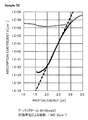
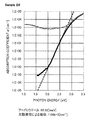
- CPM measurement the amount of light applied to the sample surface between the terminals is adjusted so that the photocurrent value is constant while a voltage is applied between the two electrodes provided on the sample, and the absorption coefficient is derived from the amount of light applied. This is done at each wavelength.
- CPM measurement when a sample has a defect, an absorption coefficient at an energy (converted from a wavelength) corresponding to the level where the defect exists is increased. By multiplying the increase in the absorption coefficient by a constant, the dDOS of the sample can be derived.
- the absorption coefficient due to the defect level can be calculated from the following equation.
- ⁇ (E) represents an absorption coefficient at each energy
- ⁇ u represents an absorption coefficient due to the back-tail.
- sample for CPM evaluation three samples (samples D1 to D3) were prepared and CPM evaluation was performed.
- a metal oxide film was formed on a glass substrate.
- a metal oxide film having a thickness of about 100 nm was formed by the same method as in sample A1.
- a metal oxide film having a thickness of about 100 nm was formed by the same method as in sample A2.
- a metal oxide film having a thickness of about 100 nm was formed by the same method as in sample A3.
- a silicon oxynitride film having a thickness of about 30 nm, a silicon oxynitride film having a thickness of about 100 nm, and a silicon oxynitride film having a thickness of about 20 nm are stacked over the metal oxide film by a plasma CVD method. .
- the oxide semiconductor film has a two-layer structure.
- the first oxide semiconductor film has a substrate temperature of 170 ° C., an oxygen gas with a flow rate of 200 sccm is introduced into the chamber of the sputtering apparatus, a pressure of 0.6 Pa, and a metal containing indium, gallium, and zinc.
- the oxide semiconductor film was removed by wet etching.
- the silicon oxynitride film was formed by a plasma CVD method using a mixed gas of SiH 4 having a flow rate of 160 sccm and N 2 O having a flow rate of 4000 sccm as a deposition gas under the conditions of a pressure of 200 Pa, a power of 1500 W, and a substrate temperature of 220 ° C. .
- the thickness of the silicon oxynitride film is about 400 nm.
- a laminated film of a Ti film having a thickness of about 50 nm, an Al film having a thickness of about 400 nm, and a Ti film having a thickness of about 100 nm was formed by a sputtering method. Thereafter, the laminated film was processed by a photolithography method to form an electrode.
- FIG. 22 shows the CPM measurement result of the sample D1
- FIG. 23 shows the CPM measurement result of the sample D2
- FIG. 24 shows the CPM measurement result of the sample D3.
- the vertical axis represents an absorption coefficient
- the horizontal axis represents light energy.
- the black solid line indicates the curve of the absorption coefficient of each sample
- the dotted line indicates the tangent
- the gray solid line indicates the optically measured absorption coefficient.
- the value of the back tail of the sample D1 estimated from FIG. 22 is 68.70 meV, and the absorption coefficient obtained by removing the absorption coefficient due to the back tail from the absorption coefficient curve, that is, the absorption coefficient due to the deep defect level.
- the value was 1.21 ⁇ 10 ⁇ 3 cm ⁇ 1 .
- the value of the back tail of the sample D2 estimated from FIG. 23 was 64.46 meV, and the value of the absorption coefficient due to the deep defect level was 1.36 ⁇ 10 ⁇ 3 cm ⁇ 1 .
- the back-tail value of sample D3 estimated from FIG. 24 was 65.83 meV, and the value of the absorption coefficient attributable to the deep defect level was 1.04 ⁇ 10 ⁇ 3 cm ⁇ 1 .
- the metal oxide film of one embodiment of the present invention can be formed by a sputtering method in an atmosphere containing oxygen.
- the substrate temperature during film formation is preferably room temperature or higher and 150 ° C. or lower, preferably 50 ° C. or higher and 150 ° C. or lower, more preferably 100 ° C. or higher and 150 ° C. or lower, typically 130 ° C.
- room temperature or higher and 150 ° C. or lower preferably 50 ° C. or higher and 150 ° C. or lower, more preferably 100 ° C. or higher and 150 ° C. or lower, typically 130 ° C.
- the flow rate ratio of oxygen during film formation is 0% to less than 50%, preferably 0% to 30%, more preferably 0% to 20%, and even more preferably 0% to 15%. % Or less, typically 10%.
- oxygen partial pressure is 0% to less than 50%, preferably 0% to 30%, more preferably 0% to 20%, and even more preferably 0% to 15%. % Or less, typically 10%.
- a metal oxide film in which a crystal part having orientation and a crystal part having no orientation are mixed can be obtained. Obtainable.
- the substrate temperature and the oxygen flow rate within the above ranges, it is possible to control the existence ratio of the crystal part having orientation and the crystal part having no orientation.
- An oxide target that can be used for forming a metal oxide film is not limited to an In—Ga—Zn-based oxide, and includes, for example, an In—M—Zn-based oxide (M is Al, Ga, Y). Or Sn) can be applied.
- a metal oxide film including a crystal part is formed using a sputtering target including a polycrystalline oxide having a plurality of crystal grains, compared to a case where a sputtering target not including a polycrystalline oxide is used, A metal oxide film having crystallinity is easily obtained.
- the sputtering target has a plurality of crystal grains and the crystal grains have a layered structure, and there is an interface that is easily cleaved, the ions are allowed to collide with the sputtering target.
- the crystal grains are cleaved.
- the sputtering target is, for example, a layered layer oriented in the c-axis direction, including In, M (M is Al, Ga, Y, or Sn), and Zn as shown in FIG. 27 described later. It shall have a structure.
- the crystal grains are tabular or pellet-like clusters, and can also be referred to as nanoclusters or pellets.
- the nanocluster 20 cleaved from the target is flat, it is easy to deposit with the plane side facing the surface of the substrate 32.
- M is Al, Ga, Y, or Sn
- Zn is oriented in the c-axis direction
- the particles 23 ejected from the target reach the surface of the substrate 32.
- the particle 23 has an aggregate of one atom or several atoms. Therefore, the particles 23 can also be referred to as atomic particles.
- the nanocluster has a layered structure oriented in the c-axis direction, including In, M (M is Al, Ga, Y, or Sn), and Zn as shown in FIG. 27 described later.
- M is Al, Ga, Y, or Sn
- Zn as shown in FIG. 27 described later.
- the particles 23 are more easily bonded to the side surfaces than the upper surface of the nanocluster 20. Accordingly, the particles 23 preferentially adhere to the side surfaces of the nanoclusters 20 so as to fill the regions where the nanoclusters 20 are not formed.
- the particle 23 is chemically connected to the nanocluster 20 to form a laterally grown portion 22 when the bond is activated (see FIG. 25A). It can also be said that the particles 23 enter the region between the nanoclusters 20.
- the lateral growth part 22 grows in the lateral direction so as to fill the region 26 between the nanoclusters 20 (the region 26 can also be referred to as Lateral Growth Buffer Region (LGBR)) (also referred to as lateral growth).
- LGBR Lateral Growth Buffer Region
- the lateral direction refers to a direction perpendicular to the c-axis in the nanocluster 20, for example.
- the particles 23 adhere to the laterally grown portions 22 of the nanoclusters 20, oxygen diffused via LGBR adheres to the particles 23, and the particles 23 again.
- the reaction of adhering in the same manner is likely to occur. It is presumed that the solid-phase growth in the horizontal direction is caused by this repetition.
- Such lateral growth of nanoclusters can also be called self-organization.
- the lateral growth portions 22 collide with each other by lateral growth of the lateral growth portions 22.
- Adjacent nanoclusters 20 are connected with a portion where the laterally growing portion 22 collides as a connecting portion 27 (see FIG. 25B). That is, the connecting portion 27 is formed in the region 26.
- the particles 23 form the lateral growth portions 22 on the side surfaces of the nanoclusters 20 and the lateral growth portions 22 grow in the lateral direction, thereby filling the regions 26 between the nanoclusters 20. . In this manner, the lateral growth portion 22 is formed until the region where the nanocluster 20 is not formed is filled.
- the gap between the nanoclusters 20 and the nanoclusters 20 is filled while the particles 23 are laterally grown, so that a clear crystal grain boundary is not formed.
- the particles 23 are smoothly connected (anchored) between the nanoclusters 20, different crystal structures are formed in the connecting portion 27 from both single crystals and polycrystals.
- a crystal structure having a strain is formed at the connecting portion 27 between the nanoclusters 20.
- the crystal structure whose upper surface has a hexagonal shape may be deformed into a pentagon or heptagon.
- a new nanocluster 20 is formed with the plane side facing the surface of the substrate 32.
- the particles 23 are deposited so as to fill the region where the nanoclusters 20 are not formed, thereby forming the lateral growth portion 22 (see FIG. 25C).
- the particles 23 adhere to the side surfaces of the nanoclusters 20 and the laterally grown portions 22 grow laterally, thereby connecting the nanoclusters 20 in the second layer (see FIG. 25D).
- Film formation continues until the m-th layer (m is an integer of 2 or more) is formed, and a metal oxide film having a stacked body is formed.
- the method for forming the metal oxide film of one embodiment of the present invention is not limited thereto, and for example, a pulse laser deposition (PLD) method, a plasma chemical vapor deposition (PECVD) method, a thermal CVD (Chemical Vapor Deposition).
- PLD pulse laser deposition
- PECVD plasma chemical vapor deposition
- thermal CVD Thermal Vapor Deposition
- an ALD (Atomic Layer Deposition) method or a vacuum deposition method may be used.
- An example of the thermal CVD method is a MOCVD (Metal Organic Chemical Vapor Deposition) method.
- the metal oxide film of one embodiment of the present invention can be applied to a semiconductor device such as a transistor.
- a metal oxide film having semiconductor characteristics hereinafter referred to as an oxide semiconductor film
- the oxide semiconductor film includes indium (In), M (M represents Al, Ga, Y, or Sn), and Zn (zinc).
- the element M is aluminum, gallium, yttrium, or tin, but as elements applicable to the element M, in addition to the above, boron, silicon, titanium, iron, nickel, germanium, zirconium, molybdenum, lanthanum, Cerium, neodymium, hafnium, tantalum, tungsten, magnesium, or the like may be used. Further, as the element M, a plurality of the aforementioned elements may be combined.
- a preferable range of the atomic ratio of indium, element M, and zinc included in the oxide semiconductor film of one embodiment of the present invention is described with reference to FIGS. 26A to 26C do not describe the atomic ratio of oxygen.
- the terms of the atomic ratio of indium, element M, and zinc included in the oxide semiconductor film are [In], [M], and [Zn].
- FIGS. 26A and 26B illustrate an example of a preferable range of the atomic ratio of indium, element M, and zinc included in the oxide semiconductor film of one embodiment of the present invention.
- FIG. 27 shows a crystal structure of InMZnO 4 when observed from a direction parallel to the b-axis.
- a metal element in a layer containing M, Zn, and oxygen hereinafter referred to as an (M, Zn) layer
- the element M or zinc represents the element M or zinc.
- the ratio of the element M and zinc shall be equal.
- the element M and zinc can be substituted and the arrangement is irregular.
- indium and element M can be substituted for each other. Therefore, the element M in the (M, Zn) layer can be replaced with indium and expressed as an (In, M, Zn) layer. In that case, a layered structure in which the In layer is 1 and the (In, M, Zn) layer is 2 is employed.
- the element M in the MZnO 2 layer can be substituted with indium, and can be expressed as an In ⁇ M 1- ⁇ ZnO 2 layer (0 ⁇ ⁇ 1). In that case, a layered structure in which the InO 2 layer is 1 and the In ⁇ M 1- ⁇ ZnO 2 layer is 2 is adopted. Further, indium in the InO 2 layer can be replaced with the element M, and can be expressed as an In 1- ⁇ M ⁇ O 2 layer (0 ⁇ ⁇ 1). In that case, the In 1- ⁇ M ⁇ O 2 layer is 1 and the MZnO 2 layer is 2.
- the In layer when the In layer is 1 and the (M, Zn) layer is non-integer, the In layer has 1 and the (M, Zn) layer has an integer of multiple layers.
- the In layer has 1 and the (M, Zn) layer has an integer of multiple layers.
- a film having an atomic ratio that deviates from the atomic ratio of the target is formed.
- [Zn] of the film may be smaller than [Zn] of the target.
- a plurality of phases may coexist in the oxide semiconductor film (two-phase coexistence, three-phase coexistence, etc.).
- a plurality of phases may coexist in the oxide semiconductor film (two-phase coexistence, three-phase coexistence, etc.).
- a grain boundary also referred to as a grain boundary
- the carrier mobility (electron mobility) of the oxide semiconductor film can be increased. This is because, in an oxide semiconductor film containing indium, element M, and zinc, the s orbital of heavy metal mainly contributes to carrier conduction, and by increasing the indium content, the region where the s orbital overlaps becomes larger. Therefore, an oxide semiconductor film with a high indium content has higher carrier mobility than an oxide semiconductor film with a low indium content.
- the oxide semiconductor film of one embodiment of the present invention have an atomic ratio shown in a region A in FIG. 26A which has a high carrier mobility and easily has a layered structure with few grain boundaries.
- An oxide semiconductor film having an atomic ratio represented by the region B is an excellent oxide semiconductor film that has particularly high crystallinity and high carrier mobility.
- the conditions under which the oxide semiconductor film forms a layered structure are not uniquely determined by the atomic ratio. Depending on the atomic ratio, there is a difference in difficulty for forming a layered structure. On the other hand, even if the atomic ratio is the same, there may be a layered structure or a layered structure depending on the formation conditions. Therefore, the region illustrated in the drawing is a region exhibiting an atomic ratio in which the oxide semiconductor film has a layered structure, and the boundaries between the regions A to C are not strict.
- Metal oxide film structure Next, the structure of the metal oxide film (hereinafter referred to as an oxide semiconductor) is described.
- An oxide semiconductor is classified into a single crystal oxide semiconductor and a non-single crystal oxide semiconductor.
- a CAAC-OS c-axis-aligned crystal oxide semiconductor
- a polycrystalline oxide semiconductor a polycrystalline oxide semiconductor
- an nc-OS nanocrystalline oxide semiconductor
- a pseudo-amorphous oxide semiconductor a-like oxide OS
- amorphous oxide semiconductor amorphous-like oxide semiconductor
- oxide semiconductors are classified into amorphous oxide semiconductors and other crystalline oxide semiconductors.
- a crystalline oxide semiconductor include a single crystal oxide semiconductor, a CAAC-OS, a polycrystalline oxide semiconductor, and an nc-OS.
- Amorphous structures are generally isotropic, have no heterogeneous structure, are metastable, have no fixed atomic arrangement, have a flexible bond angle, have short-range order, but long-range order It is said that it does not have.
- a stable oxide semiconductor cannot be called a complete amorphous semiconductor.
- an oxide semiconductor that is not isotropic (for example, has a periodic structure in a minute region) cannot be called a complete amorphous oxide semiconductor.
- an a-like OS is not isotropic but has an unstable structure having a void (also referred to as a void). In terms of being unstable, a-like OS is physically similar to an amorphous oxide semiconductor.
- CAAC-OS First, the CAAC-OS will be described.
- CAAC-OS is a kind of oxide semiconductor having a plurality of c-axis aligned crystal parts (also referred to as pellets).
- CAAC-OS is an oxide semiconductor with high crystallinity. Since the crystallinity of an oxide semiconductor may be deteriorated by entry of impurities, generation of defects, or the like, the CAAC-OS can be said to be an oxide semiconductor with few impurities and defects (such as oxygen vacancies).
- the impurity means an element other than the main components of the oxide semiconductor, such as hydrogen, carbon, silicon, or a transition metal element.
- an element such as silicon which has a stronger bonding force with oxygen than a metal element included in an oxide semiconductor, disturbs the atomic arrangement of the oxide semiconductor by depriving the oxide semiconductor of oxygen, thereby reducing crystallinity. It becomes a factor.
- heavy metals such as iron and nickel, argon, carbon dioxide, and the like have large atomic radii (or molecular radii), which disturbs the atomic arrangement of the oxide semiconductor and decreases crystallinity.
- nc-OS is analyzed by XRD.
- XRD X-ray diffraction
- Nc-OS is an oxide semiconductor having higher regularity than an amorphous oxide semiconductor. Therefore, the nc-OS has a lower density of defect states than an a-like OS or an amorphous oxide semiconductor. Note that the nc-OS does not have regularity in crystal orientation between different pellets. Therefore, the nc-OS may have a higher density of defect states than the CAAC-OS.
- the a-like OS is an oxide semiconductor having a structure between the nc-OS and an amorphous oxide semiconductor.
- A-like OS has a void or low density region. Since the a-like OS has a void, it has an unstable structure.
- the a-like OS since the a-like OS has a void, it has a structure with a lower density than the nc-OS and the CAAC-OS. Specifically, the density of the a-like OS is 78.6% or more and less than 92.3% of the density of the single crystal having the same composition. Further, the density of the nc-OS and the density of the CAAC-OS are 92.3% or more and less than 100% of the density of the single crystal having the same composition. An oxide semiconductor having a density of less than 78% of the single crystal is difficult to form.
- the density of single crystal InGaZnO 4 having a rhombohedral structure is 6.357 g / cm 3 .
- the density of a-like OS is 5.0 g / cm 3 or more and less than 5.9 g / cm 3.
- the density of the nc-OS and the density of the CAAC-OS are 5.9 g / cm 3 or more and 6.3 g / cm. less than cm 3 .
- the density corresponding to the single crystal having a desired composition can be estimated by combining single crystals having different compositions at an arbitrary ratio. What is necessary is just to estimate the density corresponding to the single crystal of a desired composition using a weighted average with respect to the ratio which combines the single crystal from which a composition differs. However, the density is preferably estimated by combining as few kinds of single crystals as possible.
- oxide semiconductors have various structures and various properties.
- the oxide semiconductor may be a stacked film including two or more of an amorphous oxide semiconductor, an a-like OS, an nc-OS, and a CAAC-OS, for example.
- an oxide semiconductor film for a transistor for example, carrier scattering at a crystal grain boundary can be reduced as compared with a transistor using polycrystalline silicon for a channel region.
- a transistor can be realized.
- a highly reliable transistor can be realized.
- the oxide semiconductor film of one embodiment of the present invention is a film in which a crystal part having orientation and a crystal part not having orientation are mixed. By using such an oxide semiconductor film having crystallinity, a transistor having both high field-effect mobility and high reliability can be realized.
- Carrier density of metal oxide film The carrier density of the metal oxide film (hereinafter referred to as an oxide semiconductor film) will be described below.
- oxygen vacancies (Vo) in the oxide semiconductor film As a factor that affects the carrier density of the oxide semiconductor film, oxygen vacancies (Vo) in the oxide semiconductor film, impurities in the oxide semiconductor film, and the like can be given.
- the density of defect states increases when hydrogen is bonded to the oxygen vacancies (this state is also referred to as VoH).
- the carrier density of the oxide semiconductor film can be controlled by controlling the density of defect states in the oxide semiconductor film.
- the object is to suppress a negative shift in the threshold voltage of the transistor or to reduce the off-state current of the transistor, it is preferable to reduce the carrier density of the oxide semiconductor film.
- the impurity concentration in the oxide semiconductor film may be decreased and the defect level density may be decreased.
- a low impurity concentration and a low density of defect states are referred to as high purity intrinsic or substantially high purity intrinsic.
- the carrier density of the high-purity intrinsic oxide semiconductor film is less than 8 ⁇ 10 15 cm ⁇ 3 , preferably less than 1 ⁇ 10 11 cm ⁇ 3 , more preferably less than 1 ⁇ 10 10 cm ⁇ 3 , and 1 ⁇ What is necessary is just to set it as 10 ⁇ -9 > cm ⁇ -3 > or more.
- the carrier density of an oxide semiconductor film it is preferable to increase the carrier density of an oxide semiconductor film.
- the impurity concentration of the oxide semiconductor film may be slightly increased or the defect state density of the oxide semiconductor film may be slightly increased.
- the band gap of the oxide semiconductor film is preferably made smaller.
- an oxide semiconductor film with a slightly high impurity concentration or a slightly high defect state density within a range where the on / off ratio of the Id-Vg characteristics of the transistor can be obtained can be regarded as substantially intrinsic.
- the oxide semiconductor film with the increased carrier density is slightly n-type. Therefore, an oxide semiconductor film with an increased carrier density may be referred to as “Slightly-n”.
- the carrier density of the substantially intrinsic oxide semiconductor film is preferably 1 ⁇ 10 5 cm ⁇ 3 or more and less than 1 ⁇ 10 18 cm ⁇ 3 , preferably 1 ⁇ 10 7 cm ⁇ 3 or more and 1 ⁇ 10 17 cm ⁇ 3 or less. More preferably, it is 1 ⁇ 10 9 cm ⁇ 3 or more and 5 ⁇ 10 16 cm ⁇ 3 or less, more preferably 1 ⁇ 10 10 cm ⁇ 3 or more and 1 ⁇ 10 16 cm ⁇ 3 or less, and further preferably 1 ⁇ 10 11 cm ⁇ 3. More preferably, it is 1 ⁇ 10 15 cm ⁇ 3 or less.
- FIG. 28 illustrates energy bands in a transistor in which an oxide semiconductor film is used for a channel region.
- FIG. 28 illustrates an example of the energy band of the gate electrode, the gate insulating film, the oxide semiconductor film, and the source or drain electrode in contact with the oxide semiconductor film.
- a silicon oxide film is used as the gate insulating film and an In—Ga—Zn oxide is used as the oxide semiconductor film.
- the transition level ( ⁇ f) of defects that can be formed in the silicon oxide film is formed at a position away from the conduction band of the gate insulating film by 3.1 eV, and the oxide when the gate voltage (Vg) is 30V.
- the Fermi level (Ef) of the silicon oxide film at the interface between the semiconductor film and the silicon oxide film is set to 3.6 eV from the conduction band of the gate insulating film. Note that the Fermi level of the silicon oxide film varies depending on the gate voltage.
- the Fermi level (Ef) of the silicon oxide film at the interface between the oxide semiconductor film and the silicon oxide film is lowered.
- a white circle in FIG. 28 represents an electron (carrier), and X in FIG. 28 represents a defect level in the silicon oxide film.
- the depth at which the Fermi level at the interface between the gate insulating film and the oxide semiconductor film is formed may be different.
- the conduction band of the gate insulating film moves upward at and near the interface between the gate insulating film and the oxide semiconductor film.
- the energy difference between the Fermi level at the interface between the gate insulating film and the oxide semiconductor film increases.
- the charge trapped in the gate insulating film is reduced.
- the change in the charge state of the defect level that can be formed in the above-described silicon oxide film is reduced, and the gate bias heat ( The variation of the threshold voltage of the transistor under stress can be reduced under stress (Gate Bias Temperature: GBT).
- the charge trapped in the defect level of the oxide semiconductor film takes a long time to disappear and may behave as if it were a fixed charge. Therefore, a transistor in which a channel region is formed in an oxide semiconductor film with a high defect level density may have unstable electrical characteristics.
- Impurities include hydrogen, nitrogen, alkali metal, alkaline earth metal, iron, nickel, silicon, and the like.
- the concentrations of silicon and carbon in the oxide semiconductor film, and the concentrations of silicon and carbon in and near the interface of the oxide semiconductor film Is 2 ⁇ 10 18 atoms / cm 3 or less, preferably 2 ⁇ 10 17 atoms / cm 3 or less.
- the concentration of alkali metal or alkaline earth metal in the oxide semiconductor film obtained by SIMS is set to 1 ⁇ 10 18 atoms / cm 3 or lower, preferably 2 ⁇ 10 16 atoms / cm 3 or lower.
- the nitrogen in the oxide semiconductor film is preferably reduced as much as possible.
- the nitrogen concentration in the oxide semiconductor film obtained by SIMS is less than 5 ⁇ 10 19 atoms / cm 3 , preferably 5 ⁇ 10 18 atoms / cm 3 or less, more preferably 1 ⁇ 10 18 atoms / cm 3 or less, and even more preferably 5 ⁇ 10 17 atoms / cm 3 or less.
- hydrogen contained in the oxide semiconductor film reacts with oxygen bonded to a metal atom to become water, so that an oxygen vacancy may be formed in some cases.
- oxygen vacancy may be formed in some cases.
- electrons serving as carriers may be generated.
- a part of hydrogen may be combined with oxygen bonded to a metal atom to generate electrons as carriers. Therefore, a transistor including an oxide semiconductor film containing hydrogen is likely to be normally on. For this reason, it is preferable that hydrogen in the oxide semiconductor film be reduced as much as possible.
- the hydrogen concentration obtained by SIMS is less than 1 ⁇ 10 20 atoms / cm 3 , preferably less than 1 ⁇ 10 19 atoms / cm 3 , more preferably 5 ⁇ 10 18 atoms / cm 3. Less than cm 3 , more preferably less than 1 ⁇ 10 18 atoms / cm 3 .
- the oxide semiconductor film preferably has an energy gap of 2 eV or more, or 2.5 eV or more.
- the thickness of the oxide semiconductor film is 3 nm to 200 nm, preferably 3 nm to 100 nm, more preferably 3 nm to 60 nm.
- the oxide semiconductor film is an In-M-Zn oxide
- Oxygen diffusion in metal oxide film The oxygen diffusion into the metal oxide film (hereinafter referred to as an oxide semiconductor film) will be described below.
- a nanocluster (also referred to as a pellet) illustrated in FIG. 29A includes two (In, M, Zn) layers (In, M (M is Al, Ga, Y, or Sn), Zn, and a layer having oxygen). ) Is formed between In layers (layers containing In and oxygen).
- an (M, Zn) layer (a layer containing M, Zn, and oxygen) may be formed instead of the (In, M, Zn) layer.
- a crystal part in which a plurality of nanoclusters are arranged so as to have orientation in the thickness direction of the film is the above-described crystal part having c-axis orientation.
- a plurality of nanoclusters have no orientation in the thickness direction of the film, and a crystal part that is oriented in various directions is a crystal part that does not have the above-described c-axis orientation.
- oxygen vacancies are easily formed in the nanocluster during the film formation.
- the oxide semiconductor film is formed under conditions in which the ratio of crystal parts having no c-axis alignment is large (for example, the film formation temperature is set to room temperature and the oxygen flow rate ratio is set to 10% or less).
- oxygen vacancies are easily formed in the nanoclusters during film formation.
- Oxygen vacancies are formed in the (In, M, Zn) layer and the In layer.
- oxygen vacancies are easily formed in the vicinity of In.
- the formation of oxygen vacancies means that oxygen existing between In, M, or Zn disappears. Therefore, when oxygen vacancies are formed, distortion occurs in the crystal structure of the (In, M, Zn) layer and In layer forming the nanocluster.
- an oxide film functioning as a sufficient oxygen supply source in contact with the oxide semiconductor film in which oxygen vacancies are formed, oxygen can be supplied from the oxide film.
- an oxide semiconductor film or an oxide insulating film containing excess oxygen may be used.
- the oxide semiconductor film for example, the above metal oxide film can be used.
- the oxide insulating film for example, silicon oxide or silicon oxynitride can be used. Note that the oxide film functioning as an oxygen supply source is not necessarily formed in contact with the oxide semiconductor film. For example, a film having oxygen permeability may be formed between an oxide film functioning as an oxygen supply source and an oxide semiconductor film.
- the atmosphere at the time of film formation may be an oxygen-excess atmosphere (for example, the film formation gas is set to 100% oxygen).
- oxygen may be added to the oxide semiconductor film or the oxide insulating film by an ion implantation method, an ion doping method, or plasma treatment.
- oxygen may be added by forming a film over the oxide semiconductor film or the oxide insulating film by a sputtering method in an atmosphere containing oxygen.
- the oxide semiconductor film functioning as an oxygen supply source when oxygen is supplied from the oxide film functioning as an oxygen supply source to the oxide semiconductor film, if the oxide semiconductor film contains excessive impurities such as water or hydrogen, the oxide semiconductor film The diffusion of oxygen inside may be hindered. Therefore, before the oxide film functioning as an oxygen supply source is formed, it is preferable to perform dehydration and dehydrogenation by performing heat treatment on the oxide semiconductor film.
- excess oxygen By forming an oxide semiconductor film in contact with the oxide film functioning as an oxygen supply source and performing heat treatment, excess oxygen (active oxygen) can be supplied from the oxide film to the oxide semiconductor film.
- active oxygen since distortion occurs in the nanocluster due to oxygen deficiency, active oxygen diffuses into the oxide semiconductor film through distortion due to oxygen deficiency.
- the diffused active oxygen compensates for oxygen vacancies formed in the surface or side surface of the nanocluster, for example, the (In, M, Zn) layer.
- oxygen deficiency can be reduced on the surface or side surface of the nanocluster, and sDOS caused by oxygen deficiency formed in the (In, M, Zn) layer can be reduced.
- the oxygen deficiency on the surface or side surface of the nanocluster is compensated, so that active oxygen is less likely to enter the nanocluster.
- hydrogen in the oxide semiconductor film is also diffused by the heat treatment. For this reason, hydrogen is trapped in oxygen vacancies formed in the nanocluster, for example, in the In layer, and VoH is easily formed inside the nanocluster. Since VoH generates carriers, the carrier density inside the nanocluster increases.
- the on-state current of the transistor can be significantly increased by increasing the carrier density inside the nanocluster. Furthermore, by reducing the sDOS on the nanocluster surface and side surfaces, the subthreshold swing value of the transistor can be reduced.
- carriers generated mainly in an In layer mainly flow at the lower end of a conduction band formed in an (In, M, Zn) layer or (M, Zn) layer. Conceivable. At this time, it is estimated that the lower end of the conduction band is mainly formed by InO x (x> 0) and ZnO x (x> 0).
- the CAC is one structure of a material in which an element included in an oxide semiconductor is unevenly distributed with a size of 0.5 nm to 10 nm, preferably 1 nm to 2 nm, or the vicinity thereof. Note that in the following, in an oxide semiconductor, one or more metal elements are unevenly distributed, and a region including the metal element has a size of 0.5 nm to 10 nm, preferably 1 nm to 2 nm, or the vicinity thereof.
- the state mixed with is also referred to as a mosaic or patch.
- CAC-IGZO in an In—Ga—Zn oxide is indium oxide (hereinafter referred to as InO X1 (X1 is a real number greater than 0)) or indium zinc oxide.
- InO X1 X1 is a real number greater than 0
- objects hereinafter, in X2 Zn Y2 O Z2 ( X2, Y2, and Z2 is larger real) than 0.
- gallium oxide hereeinafter, GaO X3 (X3 is a large real number) than 0.
- Or gallium zinc oxide hereinafter referred to as Ga X4 Zn Y4 O Z4 (X4, Y4, and Z4 are real numbers greater than 0)
- InO X1 or In X2 Zn Y2 O Z2 is uniformly distributed in the film (hereinafter also referred to as cloud shape).
- CAC-IGZO has a region GaO X3 is the main component, and In X2 Zn Y2 O Z2, or InO X1 is the main component region is a composite oxide semiconductor having a structure that is mixed.
- the first region indicates that the atomic ratio of In to the element M in the first region is larger than the atomic ratio of In to the element M in the second region. It is assumed that the concentration of In is higher than that in the second region.
- IGZO is a common name and may refer to one compound of In, Ga, Zn, and O.
- ZnO ZnO
- the crystalline compound has a single crystal structure, a polycrystalline structure, or a CAAC structure.
- the CAAC structure is a crystal structure in which a plurality of IGZO nanocrystals have c-axis orientation and are connected without being oriented in the ab plane.
- CAC relates to a material structure.
- CAC is a material structure containing In, Ga, Zn, and O, and is a region that is observed in a part of nanoparticles mainly composed of Ga, and a part of nanoparticles composed mainly of In.
- the observed region is a configuration in which the regions are randomly dispersed in a mosaic pattern. Therefore, in CAC, the crystal structure is a secondary element.
- CAC does not include a stacked structure of two or more kinds of films having different compositions.
- a structure composed of two layers of a film mainly containing In and a film mainly containing Ga is not included.
- a region GaO X3 is the main component, and In X2 Zn Y2 O Z2 or InO X1 is the main component region, in some cases clear boundary can not be observed.
- Sample structure and production method >> In the following, nine samples according to one embodiment of the present invention are described. Each sample is manufactured under different conditions for the substrate temperature and the oxygen gas flow rate ratio when the oxide semiconductor film is formed. Note that the sample has a structure including a substrate and an oxide semiconductor film over the substrate.
- a glass substrate is used as the substrate.
- an In—Ga—Zn oxide with a thickness of 100 nm is formed as an oxide semiconductor film over the glass substrate with a sputtering apparatus.
- 2500 W AC power is supplied to the oxide target installed in the sputtering apparatus.
- the substrate temperature was set to a temperature at which heating was not performed intentionally (hereinafter also referred to as RT), 130 ° C., or 170 ° C.
- RT temperature at which heating was not performed intentionally
- oxygen gas flow rate ratio nine samples are manufactured by setting the flow rate ratio of oxygen gas to the mixed gas of Ar and oxygen (hereinafter also referred to as oxygen gas flow rate ratio) to 10%, 30%, or 100%.
- FIG. 76 shows the results of measuring the XRD spectrum using the out-of-plane method.
- the upper part shows the measurement results for the sample whose substrate temperature condition during film formation is 170 ° C.
- the middle part shows the measurement results for the sample whose substrate temperature condition during film formation is 130 ° C.
- the lower part shows the measurement result during film formation.
- the measurement result in the sample is shown.
- the left column shows the measurement results for the sample with an oxygen gas flow ratio of 10%
- the center column shows the measurement results for a sample with an oxygen gas flow ratio of 30%
- the right column shows the oxygen gas flow rate.
- the measurement result in the sample whose ratio condition is 100% is shown.
- planar TEM image a planar image acquired by HAADF-STEM
- sectional image a sectional image
- the TEM image was observed using a spherical aberration correction function.
- the HAADF-STEM image was taken by irradiating an electron beam with an acceleration voltage of 200 kV and a beam diameter of about 0.1 nm ⁇ using an atomic resolution analytical electron microscope JEM-ARM200F manufactured by JEOL Ltd.
- FIG. 77A shows the substrate temperature R.D. T.A. , And a plane TEM image of a sample fabricated at an oxygen gas flow rate ratio of 10%.
- FIG. 77B shows the substrate temperature R.D. T.A. And a cross-sectional TEM image of a sample manufactured at an oxygen gas flow rate ratio of 10%.
- FIG. 77A the substrate temperature R.D. T.A. , And an electron beam diffraction pattern indicated by black spots a1, black spots a2, black spots a3, black spots a4, and black spots a5 in a planar TEM image of a sample prepared at an oxygen gas flow rate ratio of 10%.
- the observation of the electron beam diffraction pattern is performed while moving at a constant speed from the 0 second position to the 35 second position while irradiating the electron beam.
- FIG. 77C shows the result of black point a1
- FIG. 77D shows the result of black point a2
- FIG. 77E shows the result of black point a3
- FIG. 77F shows the result of black point a4, and
- FIG. 77G shows the result of black point a5.
- FIG. 77C From FIG. 77C, FIG. 77D, FIG. 77E, FIG. 77F, and FIG. 77G, it is possible to observe a high luminance region in a circle (in a ring shape). A plurality of spots can be observed in the ring-shaped region.
- FIG. T.A In the cross-sectional TEM image of the sample manufactured at an oxygen gas flow rate ratio of 10%, the electron beam diffraction pattern indicated by black spot b1, black spot b2, black spot b3, black spot b4, and black spot b5 is observed.
- FIG. 77H shows the result of black point b1
- FIG. 77I shows the result of black point b2
- FIG. 77J shows the result of black point b3
- FIG. 77K shows the result of black point b4
- FIG. 77L shows the result of black point b5.
- FIG. 77H, FIG. 77I, FIG. 77J, FIG. 77K, and FIG. A plurality of spots can be observed in the ring-shaped region.
- nc-OS oxide semiconductor having microcrystals
- a diffraction pattern such as a halo pattern is observed. Is done.
- nanobeam electron diffraction is performed on the nc-OS using an electron beam with a small probe diameter (for example, less than 50 nm)
- bright spots are observed.
- nanobeam electron diffraction is performed on the nc-OS, a region with high luminance may be observed so as to draw a circle (in a ring shape). In addition, a plurality of bright spots may be observed in the ring-shaped region.
- Substrate temperature R.D. T.A The electron beam diffraction pattern of a sample manufactured at an oxygen gas flow rate ratio of 10% has a ring-like high luminance region and a plurality of bright spots in the ring region. Therefore, the substrate temperature R.D. T.A. And the sample manufactured at an oxygen gas flow rate ratio of 10% has an electron beam diffraction pattern of nc-OS and has no orientation in the plane direction and the cross-sectional direction.
- an oxide semiconductor film with a low substrate temperature or a low oxygen gas flow ratio during deposition has properties that are clearly different from those of an amorphous oxide semiconductor film and a single crystal oxide semiconductor film. Then it can be estimated.
- each point in the analysis target region of the sample is irradiated with an electron beam, and the characteristic X-ray energy and the number of occurrences of the sample generated thereby are measured to obtain an EDX spectrum corresponding to each point.
- the peak of the EDX spectrum at each point is represented by the electron transition from the In atom to the L shell, the electron transition from the Ga atom to the K shell, the electron transition from the Zn atom to the K shell, and the K shell from the O atom.
- the ratio of each atom at each point is calculated.
- FIG. 78A, 78B, and 78C show the substrate temperature R.D. T.A. And EDX mapping in a cross section of a sample fabricated at an oxygen gas flow rate ratio of 10%.
- FIG. 78A is an EDX mapping of Ga atoms (the ratio of Ga atoms to all atoms is in the range of 1.18 to 18.64 [atomic%]).
- FIG. 78B is EDX mapping of In atoms (the ratio of In atoms to all atoms is in the range of 9.28 to 33.74 [atomic%]).
- FIG. 78C is EDX mapping of Zn atoms (the ratio of Zn atoms to all atoms is in the range of 6.69 to 24.99 [atomic%]).
- 78A, 78B, and 78C show the substrate temperature R.D. during film formation.
- T.A In a cross section of a sample manufactured at an oxygen gas flow rate ratio of 10%, a region in the same range is shown. Note that the EDX mapping shows the ratio of elements in light and dark so that the more measurement elements in the range, the brighter the brightness, and the darker the measurement elements, the darker.
- the magnification of EDX mapping shown in FIGS. 78A, 78B, and 78C is 7.2 million times.
- a range surrounded by a solid line includes many relatively dark areas, and a range surrounded by a broken line includes many relatively bright areas.
- the range surrounded by the solid line includes many relatively bright areas, and the range surrounded by the broken line includes many relatively dark areas.
- the range surrounded by the solid line is a region having a relatively large number of In atoms
- the range surrounded by a broken line is a region having a relatively small number of In atoms.
- the right side is a relatively bright region and the left side is a relatively dark region. Therefore, the range surrounded by the solid line is a region mainly composed of In X2 Zn Y2 O Z2 or InO X1 .
- a range surrounded by a solid line is a region with relatively few Ga atoms
- a range surrounded by a broken line is a region with relatively many Ga atoms.
- the upper left region is a relatively bright region
- the lower right region is a dark region. Therefore, the range surrounded by the broken line is a region whose main component is GaO X3 , Ga X4 Zn Y4 O Z4 , or the like.
- the distribution of In atoms is relatively more uniform than that of Ga atoms, and the region where InO X1 is the main component is In X2 Zn Y2 O Z2. Seems to be connected to each other through a region that is a main component. As described above, the region mainly composed of In X2 Zn Y2 O Z2 or InO X1 is formed so as to spread in a cloud shape.
- CAC-IGZO an In—Ga—Zn oxide having a structure in which a region containing GaO X3 as a main component and a region containing In X2 Zn Y2 O Z2 or InO X1 as a main component are unevenly distributed.
- the crystal structure in CAC has an nc structure.
- the nc structure possessed by CAC has several bright spots (spots) in addition to bright spots (spots) caused by IGZO including single crystal, polycrystal, or CAAC structure in an electron diffraction image.
- a crystal structure is defined as a region having a high brightness in a ring shape.
- region GaO X3 is the main component
- In X2 Zn Y2 O Z2 or the size of the area InO X1 is the main component, is, 0.5 nm or more 10nm or less, Or it is observed at 1 nm or more and 3 nm or less.
- the diameter of a region in which each metal element is a main component is 1 nm or more and 2 nm or less.
- CAC-IGZO has a structure different from that of an IGZO compound in which metal elements are uniformly distributed, and has a property different from that of an IGZO compound. That, CAC-IGZO is a region such as GaO X3 is a region which is a main component, In X2 Zn Y2 O Z2 or InO X1 is phase-separated from each other region and, in the main component, is mainly composed of the elements Has a mosaic structure.
- CAC-IGZO when CAC-IGZO is used for a semiconductor element, a high on-current can be obtained because the properties caused by GaO X3 and the like and the properties caused by In X2 Zn Y2 O Z2 or InO X1 act complementarily. (Ion) and high field effect mobility ( ⁇ ) can be realized.
- CAC-IGZO is most suitable for various semiconductor devices including a display.
- This embodiment can be implemented in combination with any of the other embodiments described in this specification or any of the other embodiments as appropriate at least part of this embodiment.
- FIGS. 30A to 30C are a top view and cross-sectional views of a transistor according to one embodiment of the present invention.
- 30A is a top view
- FIG. 30B is a cross-sectional view corresponding to the alternate long and short dash line X1-X2 shown in FIG. 30A
- FIG. 30C is a cross-sectional view corresponding to the alternate long and short dash line Y1-Y2. Note that in the top view of FIG. 30A, some elements are omitted for clarity of illustration.
- the transistor 200 includes a conductor 205 (a conductor 205a and a conductor 205b) that functions as a gate electrode, and a conductor 260 (a conductor 260a and a conductor 260b), an insulator 220 that functions as a gate insulating layer, and an insulator.
- an insulator 280 having excess oxygen and an insulator 282 having a barrier property.
- the oxide 230 includes an oxide 230a, an oxide 230b on the oxide 230a, and an oxide 230c on the oxide 230b. Note that when the transistor 200 is turned on, a current flows mainly in the oxide 230b (a channel is formed). On the other hand, although the oxide 230a and the oxide 230c may flow near the interface with the oxide 230b (may be a mixed region), other regions may function as an insulator. .
- the oxide 230c is preferably provided so as to cover the side surfaces of the oxide 230a and the oxide 230b.
- impurities such as hydrogen, water, and halogen are transferred from the insulator 280 to the oxide 230b. Diffusion can be suppressed.
- the conductor 205 includes a metal film containing an element selected from molybdenum, titanium, tantalum, tungsten, aluminum, copper, chromium, neodymium, and scandium, or a metal nitride film containing any of the above-described elements (a tantalum nitride film, A titanium nitride film, a molybdenum nitride film, a tungsten nitride film) or the like.
- a metal nitride film such as tantalum nitride is preferable because it has a barrier property against hydrogen or oxygen and is difficult to oxidize (high oxidation resistance).
- indium tin oxide indium oxide containing tungsten oxide, indium zinc oxide containing tungsten oxide, indium oxide containing titanium oxide, indium tin oxide containing titanium oxide, indium zinc oxide, silicon oxide added It is also possible to apply a conductive material such as indium tin oxide.
- FIGS. 30A to 30C illustrate a two-layer structure of the conductor 205a and the conductor 205b; however, the structure is not limited thereto, and may be a single layer or a stacked structure including three or more layers.
- a conductor having a high barrier property and a conductor having a high barrier property may be formed between a conductor having a barrier property and a conductor having a high conductivity.
- the insulator 220 and the insulator 224 are preferably insulators containing oxygen, such as a silicon oxide film and a silicon oxynitride film.
- an insulator containing excess oxygen (containing oxygen in excess of the stoichiometric composition) is preferably used. By providing such an insulator containing excess oxygen in contact with the oxide included in the transistor 200, oxygen vacancies in the oxide can be compensated.
- the insulator 222 and the insulator 224 are not necessarily made of the same material.
- the insulator 222 is formed of, for example, silicon oxide, silicon oxynitride, silicon nitride oxide, aluminum oxide, hafnium oxide, tantalum oxide, zirconium oxide, lead zirconate titanate (PZT), strontium titanate (SrTiO 3 ), or (Ba,
- An insulator containing a so-called high-k material such as Sr) TiO 3 (BST) is preferably used in a single layer or a stacked layer.
- an insulating film having a barrier property against oxygen and hydrogen, such as aluminum oxide and hafnium oxide is preferably used. When formed using such a material, the insulator 222 functions as a layer which prevents release of oxygen from the oxide 230 and entry of impurities such as hydrogen from the outside.
- aluminum oxide, bismuth oxide, germanium oxide, niobium oxide, silicon oxide, titanium oxide, tungsten oxide, yttrium oxide, or zirconium oxide may be added to these insulators.
- these insulators may be nitrided. Silicon oxide, silicon oxynitride, or silicon nitride may be stacked over the above insulator.
- the insulator 220, the insulator 222, and the insulator 224 may have a stacked structure of two or more layers. In that case, it is not limited to the laminated structure which consists of the same material, The laminated structure which consists of a different material may be sufficient.
- the insulator 222 By including the insulator 222 including a high-k material between the insulator 220 and the insulator 224, the insulator 222 can capture electrons under a specific condition and increase the threshold voltage. That is, the insulator 222 may be negatively charged.
- the operating temperature of the semiconductor device Or under a temperature higher than the storage temperature (eg, 125 ° C. or higher and 450 ° C. or lower, typically 150 ° C. or higher and 300 ° C. or lower), the potential of the conductor 205 is higher than the potential of the source electrode or the drain electrode.
- the potential of the conductor 205 is higher than the potential of the source electrode or the drain electrode.
- the threshold voltage of the transistor that captures an amount of electrons necessary for the electron trap level of the insulator 222 is shifted to the positive side. Note that the amount of electrons captured can be controlled by controlling the voltage of the conductor 205, and the threshold voltage can be controlled accordingly.
- the transistor 200 is a normally-off transistor that is non-conductive (also referred to as an off state) even when the gate voltage is 0 V.
- the process for capturing electrons may be performed in the process of manufacturing the transistor. For example, after formation of a conductor connected to the source or drain of a transistor, after completion of a previous process (wafer processing), after a wafer dicing process, after packaging, etc. Good.
- the threshold voltage can be controlled by appropriately adjusting the film thicknesses of the insulator 220, the insulator 222, and the insulator 224.
- the total thickness of the insulator 220, the insulator 222, and the insulator 220 is 65 nm or less, preferably 20 nm or less.
- a transistor having stable electrical characteristics can be provided.
- a transistor with high on-state current can be provided.
- a transistor with a small subthreshold swing value can be provided.
- a highly reliable transistor can be provided.
- a transistor with low leakage current when not conducting can be provided.
- the oxide 230a, the oxide 230b, and the oxide 230c are formed using a metal oxide such as In-M-Zn oxide (M is Al, Ga, Y, or Sn).
- M is Al, Ga, Y, or Sn.
- the oxide 230a, the oxide 230b, and the oxide 230c the metal oxide film described in the above embodiment can be used.
- the oxide 230 an In—Ga oxide, an In—Zn oxide, or the like may be used.
- the insulator I1, the oxide S1, the oxide S2, the oxide S3, and the insulator I2 illustrated in FIGS. 31A to 31C are the insulator 224, the oxide 230a, the oxide 230b, the oxide 230c, and the insulator I2 of the transistor 200, respectively. Corresponds to the body 250.
- FIG. 31A is an example of a band diagram in a film thickness direction of a stacked structure including the insulator I1, the oxide S1, the oxide S2, the oxide S3, and the insulator I2.
- FIG. 31B is an example of a band diagram in the film thickness direction of the stacked structure including the insulator I1, the oxide S2, the oxide S3, and the insulator I2.
- FIG. 31C is an example of a band diagram in the film thickness direction of the stacked structure including the insulator I1, the oxide S1, the oxide S2, and the insulator I2. Note that the band diagram shows the energy level (Ec) at the lower end of the conduction band of the insulator I1, the oxide S1, the oxide S2, the oxide S3, and the insulator I2 for easy understanding.
- Ec energy level
- the oxide S1 and the oxide S3 have an energy level at the lower end of the conduction band closer to the vacuum level than the oxide S2.
- the energy level at the lower end of the conduction band of the oxide S2, and the oxide S1 The difference from the energy level at the lower end of the conduction band of the oxide S3 is preferably 0.15 eV or more, or 0.5 eV or more, and 2 eV or less, or 1 eV or less. That is, the difference between the electron affinity of the oxides S1 and S3 and the electron affinity of the oxide S2 is preferably 0.15 eV or more, or 0.5 eV or more, and 2 eV or less, or 1 eV or less.
- the energy level at the bottom of the conduction band changes gently. In other words, it can be said that it is continuously changed or continuously joined.
- the density of defect states in the mixed layer formed at the interface between the oxide S1 and the oxide S2 or the interface between the oxide S2 and the oxide S3 is preferably low.
- the oxide S1 and the oxide S2, and the oxide S2 and the oxide S3 have a common element other than oxygen (main component), thereby forming a mixed layer with a low density of defect states.
- the oxide S2 is an In—Ga—Zn oxide
- an In—Ga—Zn oxide, a Ga—Zn oxide, a gallium oxide, or the like may be used as the oxide S1 and the oxide S3.
- the main path of the carrier is the oxide S2. Since the defect level density at the interface between the oxide S1 and the oxide S2 and the interface between the oxide S2 and the oxide S3 can be reduced, the influence on the carrier conduction due to interface scattering is small, and a high on-current is obtained. can get.
- the oxide S2 has a configuration in which the proportion of the second crystal part having no c-axis orientation is larger than that of the first crystal part having the c-axis orientation. Thus, a higher on-current can be obtained.
- the trapped electrons behave like fixed charges, so that the threshold voltage of the transistor shifts in the positive direction.
- the trap level can be kept away from the oxide S2. With this structure, the threshold voltage of the transistor can be prevented from shifting in the positive direction.
- the defect level may be farther from the vacuum level than the energy level (Ec) at the lower end of the conduction band of the oxide S2 functioning as the channel region, and electrons are likely to accumulate in the defect level. Accumulation of electrons at the defect level results in a negative fixed charge, and the threshold voltage of the transistor shifts in the positive direction. Therefore, it is preferable that the defect level be closer to the vacuum level than the energy level (Ec) at the lower end of the conduction band of the oxide S2. Thus, electrons are less likely to accumulate at the defect level, the on-state current of the transistor can be increased, and field effect mobility can be increased.
- the oxide S1 and the oxide S3 a material having a sufficiently low conductivity as compared with the oxide S2 is used.
- the oxide S2, the interface between the oxide S2 and the oxide S1, and the interface between the oxide S2 and the oxide S3 mainly function as a channel region.
- the oxide S1 and the oxide S3 have an oxide [M] / [In] of 1 or more, preferably 2 or more. Is preferably used.
- the oxide S3 it is preferable to use an oxide having [M] / ([Zn] + [In]) of 1 or more that can obtain sufficiently high insulation.
- the present invention is not limited to this.
- the energy level at the bottom of the conduction band of the oxide S2 and the bottom of the conduction bands of the oxides S1 and S3 This is preferable because the difference from the energy level can be 0.6 eV or more.
- the oxide S3 preferably has high oxygen permeability.
- the oxide S3 is preferably a metal oxide film such as the sample A1 or the sample A2 described in the above embodiment.
- the oxide S3 may be formed in an oxygen-excess atmosphere (for example, the film forming gas is set to 100% oxygen), and oxygen may be supplied from the oxide S3 to the oxide S2.
- the film forming gas is set to 100% oxygen
- the insulator 250 is formed of, for example, silicon oxide, silicon oxynitride, silicon nitride oxide, aluminum oxide, hafnium oxide, tantalum oxide, zirconium oxide, lead zirconate titanate (PZT), strontium titanate (SrTiO 3 ), or (Ba,
- An insulator containing a so-called high-k material such as Sr) TiO 3 (BST) can be used as a single layer or a stacked layer.
- aluminum oxide, bismuth oxide, germanium oxide, niobium oxide, silicon oxide, titanium oxide, tungsten oxide, yttrium oxide, or zirconium oxide may be added to these insulators.
- these insulators may be nitrided. Silicon oxide, silicon oxynitride, or silicon nitride may be stacked over the above insulator.
- the insulator 250 it is preferable to use an oxide insulator containing oxygen in excess of the stoichiometric composition, like the insulator 224. By providing such an insulator containing excess oxygen in contact with the oxide 230, oxygen vacancies in the oxide 230 can be reduced.
- the insulator 250 has a barrier property against oxygen and hydrogen such as aluminum oxide, aluminum oxynitride, gallium oxide, gallium oxynitride, yttrium oxide, yttrium oxynitride, hafnium oxide, hafnium oxynitride, and silicon nitride.
- An insulating film can be used.
- the insulator 250 is formed using such a material, it functions as a layer which prevents release of oxygen from the oxide 230 and entry of impurities such as hydrogen from the outside.
- the insulator 250 may have a stacked structure similar to that of the insulator 220, the insulator 222, and the insulator 224.
- the transistor 200 can shift the threshold voltage to the plus side.
- the transistor 200 is a normally-off transistor that is non-conductive (also referred to as an off state) even when the gate voltage is 0 V.
- a barrier film may be provided between the oxide 230 and the conductor 260 in addition to the insulator 250.
- the oxide 230c having a barrier property may be used.
- oxygen may be in a state in which the oxide substantially matches the stoichiometric composition or in a stoichiometric composition. Many supersaturated states can be obtained. In addition, entry of impurities such as hydrogen into the oxide 230 can be prevented.
- One of the conductor 240a and the conductor 240b functions as a source electrode, and the other functions as a drain electrode.
- the conductor 240a and the conductor 240b can be formed using a metal such as aluminum, titanium, chromium, nickel, copper, yttrium, zirconium, molybdenum, silver, tantalum, or tungsten, or an alloy containing the same as a main component.
- a metal nitride film such as tantalum nitride is preferable because it has a barrier property against hydrogen or oxygen and has high oxidation resistance.
- a laminated structure of two or more layers may be used.
- a tantalum nitride film and a tungsten film are preferably stacked.
- a titanium film and an aluminum film are preferably stacked.
- a two-layer structure in which an aluminum film is stacked on a tungsten film a two-layer structure in which a copper film is stacked on a copper-magnesium-aluminum alloy film, a two-layer structure in which a copper film is stacked on a titanium film, and a tungsten film A two-layer structure in which copper films are stacked may be used.
- a three-layer structure in which an aluminum film or a copper film is stacked on a titanium film or a titanium nitride film, and a titanium film or a titanium nitride film is stacked thereon, and an aluminum film or a copper film is further formed on a molybdenum film or a molybdenum nitride film, and further thereon
- a molybdenum film or a molybdenum nitride film is stacked.
- a transparent conductive material containing indium oxide, tin oxide, or zinc oxide may be used.
- the conductor 260 having a function as a gate electrode is, for example, a metal selected from aluminum, chromium, copper, tantalum, titanium, molybdenum, tungsten, an alloy containing the above-described metal as a component, or a combination of the above-described metals. It can be formed by using an alloy or the like.
- a metal nitride film such as tantalum nitride is preferable because it has a barrier property against hydrogen or oxygen and has high oxidation resistance.
- a metal selected from one or more of manganese and zirconium may be used.
- a semiconductor typified by polycrystalline silicon doped with an impurity element such as phosphorus, or silicide such as nickel silicide may be used.
- an impurity element such as phosphorus
- silicide such as nickel silicide
- the two-layer structure may be provided by laminating the same material.
- the conductor 260a is formed using a thermal CVD method, an MOCVD method, or an ALD method.
- ALD atomic layer deposition
- the conductor 260b is formed using a sputtering method.
- the conductor 260 a by including the conductor 260 a over the insulator 250, it is possible to suppress the damage during the deposition of the conductor 260 a from affecting the insulator 250. Further, since the sputtering method has a higher film formation rate than the ALD method, the yield is high and the productivity can be improved.
- a two-layer structure in which a titanium film is stacked on an aluminum film may be used.
- a two-layer structure in which a titanium film is stacked on a titanium nitride film, a two-layer structure in which a tungsten film is stacked on a titanium nitride film, and a two-layer structure in which a tungsten film is stacked on a tantalum nitride film or a tungsten nitride film are used. Also good.
- a three-layer structure in which an aluminum film is laminated on a titanium film and a titanium film is further laminated thereon may be used.
- an alloy film or a nitride film in which one or more metals selected from aluminum, titanium, tantalum, tungsten, molybdenum, chromium, neodymium, and scandium are combined may be used.
- a conductive material containing an element selected from indium, tin, zinc, gallium, silicon, or the like can be used.
- a light-transmitting conductive material such as a tin oxide or an In—Ga—Zn oxide can also be used.
- a stacked structure of the above light-transmitting conductive material and the above metal can be used.
- an insulator 280 and an insulator 282 are provided above the transistor 200.
- an oxide containing oxygen in excess of the stoichiometric composition is preferably used. That is, the insulator 280 is preferably formed with a region where oxygen is present in excess of the stoichiometric composition (hereinafter also referred to as an excess oxygen region).
- an insulator having an excess oxygen region is provided as an interlayer film or the like in the vicinity of the transistor 200 so that oxygen vacancies in the transistor 200 are reduced, so that reliability can be improved. .
- an oxide material from which part of oxygen is released by heating is preferably used as the insulator having an excess oxygen region.
- the oxide that desorbs oxygen by heating is defined as a desorption amount of oxygen of 1.0 ⁇ 10 18 atoms / in terms of oxygen atoms by thermal desorption gas analysis (TDS).
- TDS thermal desorption gas analysis
- the oxide film has a thickness of cm 3 or more, preferably 3.0 ⁇ 10 20 atoms / cm 3 or more.
- the surface temperature of the film at the time of the TDS analysis is preferably in the range of 100 ° C. to 700 ° C., or 100 ° C. to 500 ° C.
- a material containing silicon oxide or silicon oxynitride is preferably used.
- a metal oxide can be used. Note that in this specification, silicon oxynitride refers to a material with a higher oxygen content than nitrogen, and silicon nitride oxide refers to a material with a higher nitrogen content than oxygen.
- the insulator 280 that covers the transistor 200 may function as a planarization film that covers the uneven shape below the transistor 280.
- an insulating film having a barrier property against oxygen and hydrogen such as aluminum oxide and hafnium oxide, is preferably used.
- the insulator 282 may be an insulator that can be used for the insulator 222. When the insulator 282 is formed using such a material, the insulator 282 functions as a layer which prevents release of oxygen from the oxide 230 and entry of impurities such as hydrogen from the outside.
- a transistor including an oxide semiconductor with high on-state current can be provided.
- a transistor including an oxide semiconductor with low off-state current can be provided.
- variation in electrical characteristics of the semiconductor device can be suppressed and reliability can be improved.
- a semiconductor device with reduced power consumption can be provided.
- FIGS. 32A to 32C illustrate examples of structures applicable to the transistor 200.
- FIGS. FIG. 32A shows the top surface of the transistor 200. Note that some films are omitted in FIG. 32A for clarity.
- 32B is a cross-sectional view corresponding to the alternate long and short dash line X1-X2 shown in FIG. 32A
- FIG. 32C is a cross-sectional view corresponding to Y1-Y2.
- an insulator 270 is provided so as to cover the conductor 260.
- the insulator 270 is formed using a substance having a barrier property against oxygen in order to prevent the conductor 260 from being oxidized by the released oxygen.
- An insulator that can be used for the insulator 282 may be used for the insulator 270.
- a metal oxide such as aluminum oxide can be used for the insulator 270.
- the insulator 270 only needs to be provided with a thickness that prevents the conductor 260 from being oxidized.
- the thickness of the insulator 270 is 1 nm to 10 nm, preferably 3 nm to 7 nm.
- the range of material selection for the conductor 260 can be expanded.
- a material having low conductivity while having low oxidation resistance such as aluminum can be used.
- a conductor that can be easily formed or processed can be used.
- the transistor 200 with low power consumption can be provided.
- FIG. 33A to 33C illustrate an example of a structure that can be applied to the transistor 200.
- FIG. 33A shows the top surface of the transistor 200. Note that some films are omitted in FIG. 33A for clarity.
- 33B is a cross-sectional view corresponding to the alternate long and short dash line X1-X2 shown in FIG. 33A
- FIG. 33C is a cross-sectional view corresponding to Y1-Y2.
- transistor 200 illustrated in FIGS. 33A to 33C structures having the same functions as those included in the transistor 200 illustrated in FIGS. 32A to 32C are denoted by the same reference numerals.
- the insulator 243a is provided by being stacked over the conductor 240a
- the insulator 243b is provided by being stacked over the conductor 240b.
- the insulator 243a and the insulator 243b are formed with respect to oxygen in order to prevent the conductor 240a and the conductor 240b from being oxidized by the released oxygen. Therefore, a substance having a barrier property is used.
- a metal oxide such as aluminum oxide or gallium oxide can be used for the insulator 243a and the insulator 243b.
- silicon nitride or the like may be used for the insulator 243a and the insulator 243b.
- the range of material selection for the conductor 240a and the conductor 240b can be expanded.
- a material having low conductivity while having low oxidation resistance such as aluminum can be used.
- a conductor that can be easily formed or processed can be used.
- the transistor 200 with low power consumption can be provided.
- the insulator 220, the insulator 222, and the insulator 224 are stacked to function as a gate insulating film; however, the transistor described in this embodiment is not limited to this. It is not a thing.
- the transistor described in this embodiment is not limited to this. It is not a thing.
- only the insulator 224 may be provided.
- the conductor 205c is preferably provided so as to cover the upper surfaces of the conductor 205a and the conductor 205b.
- the conductors 205a to 205c may be referred to as the conductor 205 in some cases.
- the conductor 205c is formed using the same conductor as the conductor 205a in order to prevent the conductor 205b from being oxidized by the released oxygen. Can do.
- the above light-transmitting conductive material may be used.
- the range of material selection for the conductor 205b can be expanded.
- a conductor that can be easily formed or processed can be used.
- the transistor 200 with low power consumption can be provided.
- FIG. 34A shows the top surface of the transistor 200. Note that some films are omitted in FIG. 34A for clarity.
- 34B is a cross-sectional view corresponding to the alternate long and short dash line X1-X2 shown in FIG. 34A
- FIG. 34C is a cross-sectional view corresponding to Y1-Y2.
- the conductor 260 functioning as a gate electrode includes a conductor 260a, a conductor 260b, and a conductor 260c.
- the oxide 230c only needs to cover the side surface of the oxide 230b, and may be cut on the insulator 224.
- the conductor 260a is formed using a thermal CVD method, an MOCVD method, or an ALD method. In particular, it is preferable to form using the ALD method. By forming by the ALD method or the like, damage to the insulator 250 due to plasma can be reduced. Further, it is preferable because the coverage of the conductor 260a can be improved. Therefore, the transistor 200 with high reliability can be provided.
- the conductor 260b is formed using a highly conductive material such as tantalum, tungsten, copper, or aluminum. Further, the conductor 260c formed over the conductor 260b is preferably formed using a conductor having high oxidation resistance such as tungsten nitride.
- a conductor having high oxidation resistance is used for the conductor 260c having a large area in contact with the insulator 280 having an excess oxygen region, thereby preventing excess oxygen from It is possible to suppress the desorbed oxygen from being absorbed by the conductor 260. Further, oxidation of the conductor 260 can be suppressed, and oxygen released from the insulator 280 can be efficiently supplied to the oxide 230. In addition, by using a highly conductive conductor for the conductor 260b, the transistor 200 with low power consumption can be provided.
- the oxide 230b is covered with the conductor 205 and the conductor 260 in the channel width direction.
- the insulator 224 has a protrusion
- the side surface of the oxide 230 b can be covered with the conductor 260.
- the shape of the protrusion of the insulator 224 be adjusted so that the bottom surface of the conductor 260 is closer to the substrate side than the bottom surface of the oxide 230b on the side surface of the oxide 230b.
- the transistor 200 has a structure in which the oxide 230 b can be electrically surrounded by the electric fields of the conductor 205 and the conductor 260.
- the structure of the transistor that electrically surrounds the oxide 230b by the electric field of the conductor is referred to as a surrounded channel (s-channel) structure.
- a channel can be formed in the entire oxide 230b (bulk).
- the drain current of the transistor can be increased, and a larger on-current (current flowing between the source and the drain when the transistor is on) can be obtained.
- the entire region of the channel formation region formed in the oxide 230b can be depleted by the electric fields of the conductor 205 and the conductor 260. Therefore, in the s-channel structure, the off-state current of the transistor can be further reduced. Note that by reducing the channel width, the effect of increasing the on-current, the effect of reducing the off-current, and the like due to the s-channel structure can be enhanced.
- the conductor 240a and the conductor 240b are preferably formed using a conductor that has high adhesion to the oxide 230b, and the conductor 241a and the conductor 241b are preferably formed using a material having high conductivity.
- the conductor 240a and the conductor 240b are preferably formed by using an atomic layer deposition (ALD) method. By forming by ALD method or the like, the coverage can be improved.
- ALD atomic layer deposition
- titanium nitride or the like may be used for the conductor 240a and the conductor 240b.
- a highly conductive material such as tantalum, tungsten, copper, or aluminum
- the transistor 200 with high reliability and low power consumption can be provided.
- a conductor that can be used for the conductor 260 may be used as the conductor 241a and the conductor 241b.
- a light-transmitting conductor material may be used.
- FIGS. 35A to 35C illustrate examples of structures applicable to the transistor 200.
- FIGS. FIG. 35A shows the top surface of the transistor 200. Note that some films are omitted in FIG. 35A for clarity.
- 35B is a cross-sectional view corresponding to the alternate long and short dash line X1-X2 shown in FIG. 35A
- FIG. 35C is a cross-sectional view corresponding to Y1-Y2.
- transistor 200 illustrated in FIGS. 35A to 35C structures having the same functions as those included in the transistor 200 illustrated in FIGS. 30A to 30C are denoted by the same reference numerals.
- the oxide 230b is surrounded by the conductor 205 and the conductor 260 in the channel width direction.
- the insulator 222 has a convex portion, the side surface of the oxide 230 b can be covered with the conductor 260.
- the dielectric constant of the insulator 222 is large, so that the equivalent SiO 2 film thickness (EOT: Equivalent Oxide Thickness) can be reduced. . Therefore, the distance between the conductor 205 and the oxide 230 can be increased by the physical thickness of the insulator 222 without weakening the influence of the electric field from the conductor 205 on the oxide 230. Therefore, the distance between the conductor 205 and the oxide 230 can be adjusted by the thickness of the insulator 222.
- EOT Equivalent Oxide Thickness
- the shape of the protrusion of the insulator 224 be adjusted so that the bottom surface of the conductor 260 is closer to the substrate side than the bottom surface of the oxide 230b on the side surface of the oxide 230b.
- the transistor 200 has a structure in which the oxide 230 b can be electrically surrounded by the electric fields of the conductor 205 and the conductor 260.
- the structure of the transistor that electrically surrounds the oxide 230b by the electric field of the conductor is referred to as an s-channel structure.
- a channel can be formed in the entire oxide 230b (bulk).
- the drain current of the transistor can be increased, and a larger on-current (current flowing between the source and the drain when the transistor is on) can be obtained. Further, the entire region of the channel formation region formed in the oxide 230b can be depleted by the electric fields of the conductor 205 and the conductor 260. Therefore, in the s-channel structure, the off-state current of the transistor can be further reduced. Note that by reducing the channel width, the effect of increasing the on-current, the effect of reducing the off-current, and the like due to the s-channel structure can be enhanced.
- the oxide 230c may be formed so that the side surfaces of the oxide 230c substantially coincide with the side surfaces of the insulator 250 and the conductor 260. Accordingly, pattern formation of the oxide 230c, the insulator 250, and the conductor 260 can be performed at a time, so that the process can be simplified.
- a metal nitride such as tantalum nitride which has a barrier property against hydrogen or oxygen and is difficult to be oxidized (high oxidation resistance) can be used. 240b can be prevented from being oxidized. In addition, excess oxygen can be easily supplied from the insulator 280 to the oxide 230b.
- FIG. 36A to 36C illustrate examples of structures applicable to the transistor 200.
- FIG. FIG. 36A shows the top surface of the transistor 200. Note that some films are omitted in FIG. 36A for clarity.
- 36B is a cross-sectional view corresponding to the alternate long and short dash line X1-X2 shown in FIG. 36A
- FIG. 36C is a cross-sectional view corresponding to Y1-Y2.
- an oxide 230c, an insulator 250, and a conductor 260 are formed in an opening formed in the insulator 280.
- one end portion of the conductor 240a and the conductor 240b and the end portion of the opening formed in the insulator 280 coincide with each other.
- the three ends of the conductors 240 a and 240 b coincide with part of the ends of the oxide 230. Therefore, the conductor 240a and the conductor 240b can be formed at the same time as the opening of the oxide 230 or the insulator 280. Therefore, masks and processes can be reduced. In addition, yield and productivity can be improved.
- the conductor 240a, the conductor 240b, and the oxide 230b are in contact with the insulator 280 having an excess oxygen region through the oxide 230d. Therefore, the oxide 230d is interposed between the insulator 280 and the oxide 230b having a region where a channel is formed, so that impurities such as hydrogen, water, and halogen can be extracted from the insulator 280. It is possible to suppress diffusion to 230b.
- the transistor 200 illustrated in FIGS. 36A to 36C has a structure in which the conductors 240a and 240b and the conductor 260 do not overlap with each other, so that the parasitic capacitance applied to the conductor 260 can be reduced. That is, the transistor 200 having a high operating frequency can be provided.
- FIGS. 37A to 37C illustrate examples of structures applicable to the transistor 200.
- FIGS. FIG. 37A shows the top surface of the transistor 200. Note that some films are omitted in FIG. 37A for clarity.
- 37B is a cross-sectional view corresponding to the alternate long and short dash line X1-X2 shown in FIG. 37A
- FIG. 37C is a cross-sectional view corresponding to Y1-Y2.
- the transistor 200 illustrated in FIGS. 37A to 37C has a structure that does not include the oxide 230d.
- the oxide 230d is not necessarily provided. Therefore, masks and processes can be reduced. In addition, yield and productivity can be improved.
- the insulator 224 may be provided only in a region overlapping with the oxide 230a and the oxide 230b.
- the oxide 230a, the oxide 230b, and the insulator 224 can be processed using the insulator 222 as an etching stopper. Therefore, yield and productivity can be increased.
- the transistor 200 illustrated in FIGS. 37A to 37C has a structure in which the conductor 240a, the conductor 240b, and the conductor 260 do not overlap with each other, the parasitic capacitance applied to the conductor 260 can be reduced. That is, the transistor 200 having a high operating frequency can be provided.
- FIG. 38A to 38C illustrate examples of structures applicable to the transistor 200.
- FIG. FIG. 38A shows the top surface of the transistor 200. Note that some films are omitted in FIG. 38A for clarity.
- 38B is a cross-sectional view corresponding to the alternate long and short dash line X1-X2 shown in FIG. 38A
- FIG. 38C is a cross-sectional view corresponding to Y1-Y2.
- An insulator 285 and an insulator 286 are formed over the insulator 282.
- An oxide 230c, an insulator 250, and a conductor 260 are formed in openings formed in the insulator 280, the insulator 282, and the insulator 285.
- one end portion of the conductor 240a and the conductor 240b and the end portion of the opening formed in the insulator 280 coincide with each other.
- the three ends of the conductor 240a and the conductor 240b coincide with part of the ends of the oxide 230a and the oxide 230b. Therefore, the conductor 240a and the conductor 240b can be formed at the same time as the oxide 230a and the oxide 230b or the opening of the insulator 280. Therefore, masks and processes can be reduced. In addition, yield and productivity can be improved.
- the conductor 240a, the conductor 240b, and the oxide 230b are in contact with the insulator 280 having an excess oxygen region through the oxide 230d. Therefore, the oxide 230d is interposed between the insulator 280 and the oxide 230b having a region where a channel is formed, so that impurities such as hydrogen, water, and halogen can be extracted from the insulator 280. It is possible to suppress diffusion to 230b.
- the on-state current of the transistor 200 can be increased.
- FIGS. 30A to 30C An example of a method for manufacturing the semiconductor device illustrated in FIGS. 30A to 30C is described below with reference to FIGS. 39A to 42B.
- a substrate is prepared (not shown).
- a substrate that can be used as the substrate, but it is preferable that the substrate have heat resistance enough to withstand at least heat treatment performed later.
- a glass substrate such as barium borosilicate glass or alumino borosilicate glass, a ceramic substrate, a quartz substrate, a sapphire substrate, or the like can be used.
- SOI Silicon On Insulator
- GOI Germanium On Insulator
- a semiconductor device may be manufactured using a flexible substrate as the substrate.
- a transistor may be directly manufactured over a flexible substrate, or a transistor is manufactured over another manufacturing substrate, and then peeled off and transferred to the flexible substrate. Also good. Note that in order to separate the transistor from the manufacturing substrate and transfer it to the flexible substrate, a separation layer may be provided between the manufacturing substrate and the transistor including an oxide semiconductor.
- a resist mask 290 is formed over the insulator 216 using a lithography method or the like, and the insulator 214 and unnecessary portions of the insulator 216 are removed (FIG. 39A). After that, by removing the resist mask 290, an opening can be formed.
- a method of performing a slimming process on a resist mask formed by a lithography method or the like may be used.
- a dummy pattern may be formed by lithography or the like, a sidewall may be formed on the dummy pattern, the dummy pattern may be removed, and the processed film may be etched using the remaining sidewall as a resist mask.
- anisotropic dry etching as etching of the film to be processed.
- a hard mask made of an inorganic film or a metal film may be used.
- i-line wavelength 365 nm
- g-line wavelength 436 nm
- h-line wavelength 405 nm
- light used for forming the resist mask for example, i-line (wavelength 365 nm), g-line (wavelength 436 nm), h-line (wavelength 405 nm), or light obtained by mixing these can be used.
- ultraviolet light, KrF laser light, ArF laser light, or the like can be used.
- exposure may be performed by an immersion exposure technique.
- extreme ultraviolet light (EUV: Extreme-violet) or X-rays may be used as light used for exposure.
- an electron beam can be used instead of the light used for exposure. It is preferable to use extreme ultraviolet light, X-rays, or an electron beam because extremely fine processing is possible.
- a photomask is not necessary when exposure is performed by scanning a beam such as an electron beam.
- an organic resin film having a function of improving the adhesion between the film to be processed and the resist film may be formed before forming the resist film to be a resist mask.
- the organic resin film can be formed, for example, by a spin coating method so as to cover the level difference below and flatten the surface, and variations in the thickness of the resist mask provided above the organic resin film Can be reduced.
- a material that functions as an antireflection film for light used for exposure as the organic resin film.
- an organic resin film having such a function for example, there is a BARC (Bottom Anti-Reflection Coating) film.
- the organic resin film may be removed at the same time as the resist mask is removed or after the resist mask is removed.
- a conductor 205A and a conductor 205B are formed over the insulator 214 and the insulator 216.
- the conductors 205A and 205B can be formed by a sputtering method, an evaporation method, a CVD method (including a thermal CVD method, an MOCVD method, a PECVD method, or the like). In order to reduce damage caused by plasma, thermal CVD, MOCVD, or ALD is preferable (FIG. 39B).
- unnecessary portions of the conductor 205A and the conductor 205B are removed. For example, by removing a part of the conductor 205A and the conductor 205B until the insulator 216 is exposed by an etch-back process or a mechanical chemical polishing (CMP) process or the like, A conductor 205 is formed (FIG. 39C). At this time, the insulator 216 can also be used as a stopper layer, and the insulator 216 may be thin.
- CMP mechanical chemical polishing
- the CMP process is a technique for flattening the surface of a workpiece by a combined chemical and mechanical action. More specifically, a polishing cloth is attached on the polishing stage, and the polishing stage and the workpiece are rotated or swung while supplying slurry (abrasive) between the workpiece and the polishing cloth. In this method, the surface of the workpiece is polished by a chemical reaction between the slurry and the surface of the workpiece and by mechanical polishing between the polishing cloth and the workpiece.
- the CMP process may be performed only once or a plurality of times.
- the insulator 220, the insulator 222, and the insulator 224 are formed (FIG. 39D).
- the insulator 220, the insulator 222, and the insulator 224 can be manufactured using the above-described materials or materials that can be used for the insulator 320 described later.
- the insulator 222 is preferably formed using a high-k material such as hafnium oxide.
- the insulator 220, the insulator 222, and the insulator 224 are formed by, for example, a sputtering method, a chemical vapor deposition (CVD) method (thermal CVD method, a metal organic chemical vapor deposition (MOCVD) method, a chemical organic vapor deposition (MOCVD) method, Plasma excitation CVD (including PECVD: Plasma Enhanced Chemical Vapor Deposition) method, molecular epitaxy (MBE) method, atomic layer deposition (ALD: Atomic Layer Deposition Laser deposition) ) Method etc. Kill.
- CVD chemical vapor deposition
- MOCVD metal organic chemical vapor deposition
- MOCVD chemical organic vapor deposition
- Plasma excitation CVD including PECVD: Plasma Enhanced Chemical Vapor Deposition
- MBE molecular epitaxy
- ALD Atomic Layer Deposition Laser deposition
- a silicon oxide film with good step coverage formed by reacting TEOS (Tetra-Ethyl-Ortho-Silicate) or silane with oxygen, nitrous oxide, or the like can be used.
- the insulator 220, the insulator 222, and the insulator 224 are preferably formed successively. By forming a film continuously, an insulator with high reliability can be formed without an impurity adhering to the interface between the insulator 220 and the insulator 222 and the interface between the insulator 222 and the insulator 224. it can.
- an oxide 230A to be the oxide 230a and an oxide 230B to be the oxide 230b are sequentially formed.
- the description of the metal oxide in the above embodiment can be referred to.
- the oxide is preferably formed continuously without being exposed to the air.
- the oxide 230A and the oxide 230B are preferable because the film density can be increased by a sputtering method.
- a rare gas typically argon
- oxygen or a mixed gas of a rare gas and oxygen is used as the sputtering gas as appropriate.
- the sputtering gas is preferably highly purified. For example, by using oxygen gas or argon gas highly purified to a dew point of ⁇ 60 ° C. or lower, preferably ⁇ 100 ° C. or lower as a sputtering gas, moisture or the like can be taken into the oxide semiconductor film 108 as much as possible. Can be prevented.
- an adsorption method such as a cryopump is used to remove as much water as possible from the oxide 230A and the oxide 230B in the chamber in the sputtering apparatus. It is preferable to evacuate to a high vacuum (from about 5 ⁇ 10 ⁇ 7 Pa to about 1 ⁇ 10 ⁇ 4 Pa) using a vacuum exhaust pump.
- a conductive film 240A to be the conductor 240a and the conductor 240b is formed over the oxide 230A.
- the conductive film 240A is preferably formed using a material that has a barrier property against hydrogen or oxygen and also has high oxidation resistance.
- a resist mask 292 is formed by the same method as described above (FIG. 39E).
- unnecessary portions of the conductive film 240A are removed by etching to form an island-shaped conductive layer 240B (FIG. 40A). After that, unnecessary portions of the oxide 230a and the oxide 230b are removed by etching using the conductive layer 240B as a mask.
- the insulator 224 may be processed into an island shape at the same time.
- the insulator 222 having a barrier property as an etching stopper film even in a structure in which the total thickness of the insulator 220, the insulator 222, and the insulator 224 is thin, over-etching is performed up to the wiring layer below. Can be prevented. Further, by reducing the total film thickness of the insulator 220, the insulator 222, and the insulator 224, a voltage from the conductor 205 is efficiently applied, so that a transistor with low power consumption can be provided.
- the heat treatment may be performed at a temperature of 250 ° C. to 400 ° C., preferably 320 ° C. to 380 ° C., in an inert gas atmosphere, an atmosphere containing an oxidizing gas of 10 ppm or more, or in a reduced pressure state.
- the heat treatment may be performed in an atmosphere containing 10 ppm or more of an oxidizing gas in order to supplement the desorbed oxygen after the heat treatment in an inert gas atmosphere.
- hydrogen or water which is an impurity of the oxide 230a and the oxide 230b can be removed.
- oxygen is supplied to the oxide 230a and the oxide 230b from the insulator formed below the oxide 230a, so that oxygen vacancies in the oxide can be reduced.
- a resist mask 294 is formed on the island-like conductive layer 240B by the same method as described above (FIG. 40D). Subsequently, after unnecessary portions of the conductive film are removed by etching, the resist mask 294 is removed, whereby the conductors 240a and 240b are formed (FIG. 41A). At this time, the insulator 224 or the insulator 222 may be over-etched to have an s-channel structure.
- the heat treatment may be performed at a temperature of 250 ° C. to 400 ° C., preferably 320 ° C. to 380 ° C., in an inert gas atmosphere, an atmosphere containing an oxidizing gas of 10 ppm or more, or in a reduced pressure state.
- the heat treatment may be performed in an atmosphere containing 10 ppm or more of an oxidizing gas in order to supplement the desorbed oxygen after the heat treatment in an inert gas atmosphere.
- hydrogen or water which is an impurity of the oxide 230a and the oxide 230b can be removed.
- oxygen is supplied to the oxide 230a and the oxide 230b from the insulator formed below the oxide 230a, so that oxygen vacancies in the oxide can be reduced. Further, in the case where heat treatment is performed with an oxidizing gas, oxygen vacancies in the region where the channel is formed can be efficiently reduced by contacting the oxidizing gas directly with the region where the channel is formed.
- an oxide 230c, an insulator 250, and a conductive film 260A to be the conductor 260 are sequentially formed.
- the description of the metal oxide in the above embodiment can be referred to.
- the conductive film 260A is preferably formed using a material having a barrier property against hydrogen or oxygen and high oxidation resistance.
- a single layer is shown in the figure, a stacked structure of two or more layers may be used.
- a two-layer structure may be provided by laminating the same material.
- the first conductive film is formed using a thermal CVD method, an MOCVD method, or an ALD method.
- ALD method it is preferable to form using the ALD method.
- the second conductive film is formed using a sputtering method.
- the first conductive film over the insulator 250, it is possible to suppress the damage during the deposition of the second conductive film from affecting the insulator 250.
- the sputtering method has a higher film formation rate than the ALD method, the yield is high and the productivity can be improved.
- the conductive film 260A be formed using a deposition gas that does not contain chlorine.
- a resist mask 296 is formed on the conductive film 260A by the same method as described above (FIG. 41C). Subsequently, unnecessary portions of the conductive film 260A are removed by etching to form the conductor 260, and then the resist mask 296 is removed (FIG. 41D).
- the insulator 280 is an insulator containing oxygen, such as a silicon oxide film or a silicon oxynitride film.
- oxygen such as a silicon oxide film or a silicon oxynitride film.
- a silicon oxide film or a silicon oxynitride film in which a large amount of oxygen is contained in the film can be formed by appropriately setting deposition conditions in a CVD method or a sputtering method.
- oxygen may be added by an ion implantation method, an ion doping method, or plasma treatment after the silicon oxide film or the silicon oxynitride film is formed.
- a typical oxygen plasma treatment is to treat the surface of an oxide semiconductor with radicals generated by glow discharge plasma of oxygen gas.
- oxygen gas As a gas for generating plasma, not only oxygen but also oxygen gas and rare gas are used.
- the mixed gas may be used.
- the temperature may be 250 ° C. or higher and 400 ° C. or lower, preferably 300 ° C. or higher and 400 ° C. or lower, in an atmosphere containing an oxidizing gas or in a reduced pressure state.
- the insulator 280 and the oxide 230 are dehydrated or dehydrogenated, and an excess oxygen region can be formed by introducing excess oxygen into the insulator 280.
- oxygen vacancies are generated in the dehydrated or dehydrogenated oxide 230, and the resistance is reduced.
- oxygen deficiency in the oxide 230 is filled with excess oxygen in the insulator 280. Therefore, by the oxygen plasma treatment, the insulator 280 and the oxide 230 can remove hydrogen or water as impurities while filling oxygen vacancies. Accordingly, improvement in electrical characteristics of the transistor 200 and variation in electrical characteristics can be reduced.
- an insulator 282 is formed on the insulator 280.
- the insulator 282 is preferably formed with a sputtering apparatus. By using the sputtering method, an excess oxygen region can be easily formed in the insulator 280 which is the lower layer of the insulator 282.
- ions and sputtered particles exist between the target and the substrate.
- the target is connected to a power source and is supplied with the potential E0.
- the substrate is given a potential E1 such as a ground potential.
- the substrate may be electrically floating.
- the ions in the plasma are accelerated by the potential difference E2-E0 and collide with the target, so that the sputtered particles are ejected from the target.
- the sputtered particles adhere to and deposit on the film formation surface to form a film.
- some ions recoil by the target and may be taken into the insulator 280 below the formed film through the film formed as recoil ions.
- ions in the plasma are accelerated by the potential difference E2-E1, and impact the film formation surface. At this time, some ions reach the inside of the insulator 280.
- a region into which the ions are taken is formed in the insulator 280. That is, when the ions are oxygen-containing ions, an excess oxygen region is formed in the insulator 280.
- An excess oxygen region can be formed by introducing excess oxygen into the insulator 280.
- Excess oxygen in the insulator 280 is supplied to the oxide 230 by heat treatment at a temperature of, for example, 200 ° C. or higher and 450 ° C. or lower, preferably 320 ° C. or higher and 380 ° C. or lower. Can be compensated.
- the substrate is heated at the above temperature, so that oxygen is supplied to the oxide 230 without additional heating after the film formation. can do.
- the oxide 230c is an oxide having high oxygen permeability, oxygen can be easily diffused from the insulator 280 to the oxide 230b.
- excess oxygen is bonded to the side surface of the crystal part having orientation.
- a metal such as In, M, or Zn is bonded to the bonded active oxygen.
- the active oxygen and a metal such as In, M, or Zn are repeatedly bonded to each other so that solid phase growth occurs laterally from the side surface of the crystal part having orientation.
- heat treatment is performed on the oxide 230a and the oxide 230b in advance, and dehydration and dehydrogenation are performed, whereby impurities such as water or hydrogen contained in the oxide 230 are removed. It can be reduced. Accordingly, the diffusion of oxygen due to impurities such as water or hydrogen contained in the oxide 230 is reduced, so that oxygen can be supplied to the oxide 230 more efficiently.
- the transistor 200 of one embodiment of the present invention can be manufactured.
- FIGS. 43A to 49B One example of a semiconductor device (memory device) using a capacitor which is one embodiment of the present invention is illustrated in FIGS. 43A to 49B.
- FIG. 43A is a circuit diagram of FIGS. 44 to 47 and FIGS. 49A to 51.
- 48A and 48B and FIGS. 49A and 49B show end portions of regions where the semiconductor devices shown in FIGS. 44 to 47 and FIGS. 49A to 51 are formed.
- the semiconductor device illustrated in FIGS. 43A and 44 to 47 includes the transistor 300, the transistor 200, and the capacitor 100.
- the transistor 200 is a transistor in which a channel is formed in a semiconductor layer including an oxide semiconductor. Since the transistor 200 has a small off-state current, stored data can be held for a long time by using the transistor 200 for a semiconductor device (memory device). In other words, the semiconductor device (memory device) which does not require a refresh operation or has a very low frequency of the refresh operation can be used, so that power consumption can be sufficiently reduced.
- the wiring 3001 is electrically connected to the source of the transistor 300, and the wiring 3002 is electrically connected to the drain of the transistor 300.
- the wiring 3003 is electrically connected to one of a source and a drain of the transistor 200, and the wiring 3004 is electrically connected to the gate of the transistor 200.
- the gate of the transistor 300 and the other of the source and the drain of the transistor 200 are electrically connected to one of the electrodes of the capacitor 100, and the wiring 3005 is electrically connected to the other of the electrodes of the capacitor 100. .
- the semiconductor device illustrated in FIG. 43A has a characteristic that the potential of the gate of the transistor 300 can be held, so that information can be written, held, and read as described below.
- the potential of the fourth wiring 3004 is set to a potential at which the transistor 200 is turned on, so that the transistor 200 is turned on. Accordingly, the potential of the third wiring 3003 is supplied to the node FG that is electrically connected to one of the gate of the transistor 300 and the electrode of the capacitor 100. That is, predetermined charge is given to the gate of the transistor 300 (writing).
- predetermined charge is given to the gate of the transistor 300 (writing).
- the potential of the fourth wiring 3004 is set to a potential at which the transistor 200 is turned off and the transistor 200 is turned off, so that charge is held at the node FG (holding).
- the second wiring 3002 has a charge held in the node FG. Take a potential according to the amount. This is because, when the transistor 300 is an n-channel type, the apparent threshold voltage V th_H when the gate of the transistor 300 is supplied with a high level charge is the low level charge applied to the gate of the transistor 300. This is because it becomes lower than the apparent threshold voltage V th_L in the case of being present.
- the apparent threshold voltage refers to the potential of the fifth wiring 3005 necessary for bringing the transistor 300 into a “conductive state”.
- the potential of the fifth wiring 3005 when the potential of the fifth wiring 3005 is set to a potential V 0 between V th_H V th_L , the charge given to the node FG can be determined. For example, in writing, when a high-level charge is applied to the node FG, the transistor 300 is turned “on” when the potential of the fifth wiring 3005 is V 0 (> V th_H ). On the other hand, when a low-level charge is supplied to the node FG, the transistor 300 remains in a “non-conduction state” even when the potential of the fifth wiring 3005 becomes V 0 ( ⁇ V th_L ). Therefore, by determining the potential of the second wiring 3002, information held in the node FG can be read.
- a memory device (memory cell array) can be configured by arranging the semiconductor devices illustrated in FIG. 43A in a matrix.
- a potential that causes the transistor 300 to be “non-conductive” regardless of the charge applied to the node FG, that is, a potential lower than V th_H is supplied to the fifth wiring 3005.
- the fifth wiring 3005 is supplied with a potential at which the transistor 300 becomes “conductive” regardless of the charge applied to the node FG, that is, a potential higher than V th_L.
- the semiconductor device illustrated in FIG. 43B is different from the semiconductor device illustrated in FIG. 43A in that the transistor 300 is not included. In this case as well, information can be written and held by the same operation as that of the semiconductor device shown in FIG. 43A.
- Reading of information in the semiconductor device illustrated in FIG. 43B is described.
- the transistor 200 When the transistor 200 is turned on, the third wiring 3003 in a floating state and the capacitor 100 are brought into conduction, and charge is redistributed between the third wiring 3003 and the capacitor 100.
- the potential of the third wiring 3003 changes.
- the amount of change in potential of the third wiring 3003 varies depending on one potential of the electrode of the capacitor 100 (or charge accumulated in the capacitor 100).
- the potential of one electrode of the capacitor 100 is V
- the capacitance of the capacitor 100 is C
- the capacitance component of the third wiring 3003 is CB
- the potential of the third wiring 3003 before charge is redistributed is (CB ⁇ VB0 + C ⁇ V) / (CB + C). Therefore, when the potential of one of the electrodes of the capacitor 100 assumes two states of V1 and V0 (V1> V0) as the state of the memory cell, the third wiring 3003 in the case where the potential V1 is held.
- information can be read by comparing the potential of the third wiring 3003 with a predetermined potential.
- a transistor to which the first semiconductor is applied is used as a driver circuit for driving a memory cell, and a transistor to which the second semiconductor is applied is stacked on the driver circuit as the transistor 200. do it.
- memory contents can be held for a long time by using a transistor with an off-state current that is formed using an oxide semiconductor. That is, a refresh operation is unnecessary or the frequency of the refresh operation can be extremely low, so that a semiconductor device with low power consumption can be realized.
- stored data can be held for a long time even when power is not supplied (note that a potential is preferably fixed).
- the semiconductor device does not require a high voltage for writing information, the element is hardly deteriorated.
- the semiconductor device since electrons are not injected into the floating gate and electrons are not extracted from the floating gate, there is no problem of deterioration of the insulator.
- the semiconductor device according to one embodiment of the present invention has no limitation on the number of rewritable times, and is a semiconductor device in which reliability is dramatically improved. Further, since data is written depending on the conductive state and non-conductive state of the transistor, high-speed operation is possible.
- a semiconductor device of one embodiment of the present invention includes a transistor 300, a transistor 200, and a capacitor 100 as illustrated in FIG.
- the transistor 200 is provided above the transistor 300
- the capacitor 100 is provided above the transistor 300 and the transistor 200.
- the transistor 300 includes a conductor 316, an insulator 314, a semiconductor region 312 formed of part of the substrate 311, a low resistance region 318a functioning as a source region or a drain region, and a low resistance region 318b. Have.
- the transistor 300 may be either a p-channel type or an n-channel type.
- the region in which the channel of the semiconductor region 312 is formed, the region in the vicinity thereof, the low resistance region 318a serving as the source region or the drain region, the low resistance region 318b, and the like preferably include a semiconductor such as a silicon-based semiconductor. It preferably contains crystalline silicon. Alternatively, a material containing Ge (germanium), SiGe (silicon germanium), GaAs (gallium arsenide), GaAlAs (gallium aluminum arsenide), or the like may be used. A structure using silicon in which effective mass is controlled by applying stress to the crystal lattice and changing the lattice spacing may be employed. Alternatively, the transistor 300 may be a HEMT (High Electron Mobility Transistor) by using GaAs, GaAlAs, or the like.
- HEMT High Electron Mobility Transistor
- the low-resistance region 318 a and the low-resistance region 318 b provide an n-type conductivity element such as arsenic or phosphorus, or a p-type conductivity property such as boron, in addition to the semiconductor material applied to the semiconductor region 312. Containing elements.
- the conductor 316 functioning as a gate electrode includes a semiconductor material such as silicon, a metal material, an alloy containing an element imparting n-type conductivity such as arsenic or phosphorus, or an element imparting p-type conductivity such as boron.
- a conductive material such as a material or a metal oxide material can be used.
- the threshold voltage can be adjusted by determining the work function depending on the material of the conductor. Specifically, it is preferable to use a material such as titanium nitride or tantalum nitride for the conductor. Further, in order to achieve both conductivity and embeddability, it is preferable to use a metal material such as tungsten or aluminum as a laminate for the conductor, and tungsten is particularly preferable from the viewpoint of heat resistance.
- the semiconductor region 312 (a part of the substrate 311) where a channel is formed has a convex shape.
- the conductor 316 is provided so as to cover a side surface and an upper surface of the semiconductor region 312 with an insulator 314 interposed therebetween.
- the conductor 316 may be formed using a material that adjusts a work function.
- Such a transistor 300 is also called a FIN-type transistor because it uses a convex portion of a semiconductor substrate.
- an insulator functioning as a mask for forming the convex portion may be provided in contact with the upper portion of the convex portion.
- the transistor 300 illustrated in FIGS. 44A and 44B is an example and is not limited to the structure, and an appropriate transistor may be used depending on a circuit configuration or a driving method.
- the structure of the transistor 300 may be provided as a planar type. In the circuit configuration illustrated in FIG. 43B, the transistor 300 is not necessarily provided.
- the insulator 320, the insulator 322, the insulator 324, and the insulator 326 are stacked in this order so as to cover the transistor 300.
- the insulator 320, the insulator 322, the insulator 324, and the insulator 326 for example, silicon oxide, silicon oxynitride, silicon nitride oxide, silicon nitride, aluminum oxide, aluminum oxynitride, aluminum nitride oxide, aluminum nitride, or the like is used. That's fine.
- the insulator 322 functions as a flattening film for flattening a step generated by the transistor 300 or the like provided thereunder.
- the top surface of the insulator 322 may be planarized by a planarization process using a CMP process or the like in order to improve planarity.
- a film having a barrier property such that hydrogen or impurities are not diffused from the substrate 311 or the transistor 300 to a region where the transistor 200 is provided is preferably used.
- silicon nitride formed by a CVD method can be used as an example of a film having a barrier property against hydrogen.
- silicon nitride formed by a CVD method when hydrogen diffuses into a semiconductor element including an oxide semiconductor such as the transistor 200, characteristics of the semiconductor element may be reduced. Therefore, a film for suppressing hydrogen diffusion is preferably used between the transistor 200 and the transistor 300.
- the film that suppresses the diffusion of hydrogen is a film with a small amount of hydrogen desorption.
- the amount of hydrogen desorption can be analyzed using, for example, TDS analysis.
- the amount of hydrogen desorbed from the insulator 324 is 10 ⁇ 10 5 in terms of the amount of desorbed hydrogen atoms converted to hydrogen atoms per area of the insulator 324 in the range of 50 ° C. to 500 ° C. in TDS analysis. It may be 15 atoms / cm 2 or less, preferably 5 ⁇ 10 15 atoms / cm 2 or less.
- the insulator 326 preferably has a lower dielectric constant than the insulator 324.
- the dielectric constant of the insulator 326 is preferably less than 4, and more preferably less than 3.
- the relative dielectric constant of the insulator 324 is preferably equal to or less than 0.7 times that of the insulator 326, and more preferably equal to or less than 0.6 times.
- the insulator 320, the insulator 322, the insulator 324, and the insulator 326 are embedded with a conductor 328, a conductor 330, and the like that are electrically connected to the capacitor 100 or the transistor 200.
- the conductor 328 and the conductor 330 function as plugs or wirings.
- a conductor having a function as a plug or a wiring may be given the same reference numeral by collecting a plurality of structures.
- the wiring and the plug electrically connected to the wiring may be integrated. That is, a part of the conductor may function as a wiring, and a part of the conductor may function as a plug.
- a conductive material such as a metal material, an alloy material, a metal nitride material, or a metal oxide material is used as a single layer or a stacked layer.
- a high melting point material such as tungsten or molybdenum that has both heat resistance and conductivity, and it is preferable to use tungsten.
- a low-resistance conductive material such as aluminum or copper. Wiring resistance can be lowered by using a low-resistance conductive material.
- a wiring layer may be provided over the insulator 326 and the conductor 330.
- an insulator 350, an insulator 352, and an insulator 354 are sequentially stacked.
- a conductor 356 is formed in the insulator 350, the insulator 352, and the insulator 354.
- the conductor 356 functions as a plug or a wiring. Note that the conductor 356 can be provided using a material similar to that of the conductor 328 and the conductor 330.
- the insulator 350 is preferably an insulator having a barrier property against hydrogen, similarly to the insulator 324.
- the conductor 356 preferably includes a conductor having a barrier property against hydrogen.
- a conductor having a barrier property against hydrogen is formed in an opening portion of the insulator 350 having a barrier property against hydrogen.
- tantalum nitride may be used as the conductor having a barrier property against hydrogen. Further, by stacking tantalum nitride and tungsten having high conductivity, diffusion of hydrogen from the transistor 300 can be suppressed while maintaining conductivity as a wiring. In this case, it is preferable that the tantalum nitride layer having a barrier property against hydrogen be in contact with the insulator 350 having a barrier property against hydrogen.
- the insulator 358, the insulator 210, the insulator 212, the insulator 213, the insulator 214, and the insulator 216 are sequentially stacked over the insulator 354.
- a substance having a barrier property against oxygen or hydrogen is preferably used for any or all of the insulator 358, the insulator 210, the insulator 212, the insulator 213, the insulator 214, and the insulator 216.
- a film having a barrier property so that hydrogen and impurities do not diffuse from a region where the substrate 311 or the transistor 300 is provided to a region where the transistor 200 is provided for example.
- a material similar to that of the insulator 324 can be used.
- silicon nitride formed by a CVD method can be used as an example of a film having a barrier property against hydrogen.
- silicon nitride formed by a CVD method when hydrogen diffuses into a semiconductor element including an oxide semiconductor such as the transistor 200, characteristics of the semiconductor element may be reduced. Therefore, a film for suppressing hydrogen diffusion is preferably used between the transistor 200 and the transistor 300.
- the film that suppresses the diffusion of hydrogen is a film with a small amount of hydrogen desorption.
- a metal oxide such as aluminum oxide, hafnium oxide, or tantalum oxide.
- aluminum oxide has a high blocking effect that prevents the film from permeating both oxygen and impurities such as hydrogen and moisture that cause fluctuations in the electrical characteristics of the transistor. Therefore, aluminum oxide can prevent impurities such as hydrogen and moisture from entering the transistor 200 during and after the manufacturing process of the transistor. In addition, release of oxygen from the oxide included in the transistor 200 can be suppressed. Therefore, it is suitable for use as a protective film for the transistor 200.
- the insulator 210 and the insulator 216 can be formed using the same material as the insulator 320.
- the insulator 216 a silicon oxide film, a silicon oxynitride film, or the like can be used.
- the insulator 358, the insulator 210, the insulator 212, the insulator 213, the insulator 214, and the insulator 216 are embedded with a conductor 218, a conductor (the conductor 205) included in the transistor 200, and the like. ing.
- the conductor 218 functions as a plug or a wiring electrically connected to the capacitor 100 or the transistor 300.
- the conductor 218 can be provided using a material similar to that of the conductor 328 and the conductor 330.
- the insulator 358, the insulator 212, the insulator 213, and the conductor 218 in a region in contact with the insulator 214 are preferably conductors having a barrier property against oxygen, hydrogen, and water.
- the transistor 300 and the transistor 200 are layers having a barrier property against oxygen, hydrogen, and water and can be completely separated, so that diffusion of hydrogen from the transistor 300 to the transistor 200 can be suppressed. .
- a transistor 200 is provided above the insulator 216. Note that the transistor described above may be used as the structure of the transistor 200.
- a transistor 200 illustrated in FIGS. 44A and 44B is an example and is not limited to the structure, and an appropriate transistor may be used depending on a circuit configuration or a driving method.
- An insulator 280 is provided over the transistor 200.
- an insulator containing oxygen in excess of the stoichiometric composition is preferably used. That is, the insulator 280 is preferably formed with a region where oxygen is present in excess of the stoichiometric composition (hereinafter also referred to as an excess oxygen region).
- an excess oxygen region is provided as an interlayer film or the like in the vicinity of the transistor 200, so that oxygen vacancies in the transistor 200 are reduced and reliability is improved. Can do.
- an oxide material from which part of oxygen is released by heating is preferably used as the insulator having an excess oxygen region.
- the oxide oxygen is released by heating, by TDS, the amount of released oxygen converted into oxygen atoms 1.0 ⁇ 10 18 atoms / cm 3 or more, preferably 3.0 ⁇ 10 20
- the surface temperature of the film at the time of the TDS analysis is preferably in the range of 100 ° C. to 700 ° C., or 100 ° C. to 500 ° C.
- a material containing silicon oxide or silicon oxynitride is preferably used.
- a metal oxide can be used. Note that in this specification, silicon oxynitride refers to a material with a higher oxygen content than nitrogen, and silicon nitride oxide refers to a material with a higher nitrogen content than oxygen.
- the insulator 280 that covers the transistor 200 may function as a planarization film that covers the uneven shape below the transistor 280. Further, a conductor 244 and the like are embedded in the insulator 280.
- the conductor 244 functions as a plug or a wiring electrically connected to the capacitor 100, the transistor 200, or the transistor 300.
- the conductor 244 can be provided using a material similar to that of the conductor 328 and the conductor 330.
- the conductor 244 when the conductor 244 is provided in a stacked structure, it is preferable to include a conductor having high oxidation resistance.
- a conductor having high oxidation resistance is preferably provided in a region in contact with the insulator 280 having an excess oxygen region.
- the conductor 244 can suppress excessive oxygen from the insulator 280.
- the conductor 244 preferably includes a conductor having a barrier property against hydrogen.
- impurities such as hydrogen in a region in contact with the insulator 280 having an excess oxygen region
- a barrier layer 245 may be provided over the conductor 244. By including the barrier layer 245, diffusion of impurities contained in the conductor 244 and part of the elements of the conductor 244 can be suppressed.
- a metal oxide such as aluminum oxide, hafnium oxide, or tantalum oxide, or a metal nitride such as tantalum nitride is preferably used.
- aluminum oxide has a high blocking effect that prevents the film from permeating both oxygen and impurities such as hydrogen and moisture, which cause variation in electrical characteristics of the transistor. Therefore, aluminum oxide can prevent impurities such as hydrogen and moisture from entering the transistor 200 during and after the manufacturing process of the transistor.
- an insulator 282, an insulator 283, an insulator 284, and an insulator 110 are sequentially stacked.
- a conductor 124 and the like are embedded in the insulator 282, the insulator 283, the insulator 284, and the insulator 110.
- the conductor 124 functions as a plug or a wiring electrically connected to the capacitor 100, the transistor 200, or the transistor 300.
- the conductor 124 can be provided using a material similar to that of the conductor 356.
- the insulator 282 can be formed using a material similar to that of the insulator 214.
- the insulator 283 can be formed using a material similar to that of the insulator 213.
- an insulator similar to the insulator 212 can be used.
- the insulator 110 can be formed using a material similar to that of the insulator 216.
- a metal oxide such as aluminum oxide, hafnium oxide, or tantalum oxide is preferably used.
- aluminum oxide has a high blocking effect that prevents the film from permeating both oxygen and impurities such as hydrogen and moisture that cause fluctuations in the electrical characteristics of the transistor. Therefore, aluminum oxide can prevent impurities such as hydrogen and moisture from entering the transistor 200 during and after the manufacturing process of the transistor. In addition, release of oxygen from the oxide included in the transistor 200 can be suppressed. Therefore, aluminum oxide is suitable for use as a protective film for the transistor 200.
- a film having a barrier property so that hydrogen and impurities do not diffuse from the region where the capacitor 100 is provided to the region where the transistor 200 is provided as the insulator 284. Therefore, a material similar to that of the insulator 324 can be used.
- silicon nitride formed by a CVD method can be used as an example of a film having a barrier property against hydrogen.
- silicon nitride formed by a CVD method when hydrogen diffuses into a semiconductor element including an oxide semiconductor such as the transistor 200, characteristics of the semiconductor element may be reduced. Therefore, a film for suppressing hydrogen diffusion is preferably used between the transistor 200 and the transistor 300.
- the film that suppresses the diffusion of hydrogen is a film with a small amount of hydrogen desorption.
- the transistor 200 and the insulator 280 including an excess oxygen region are sandwiched between the stacked structure of the insulator 212, the insulator 213, and the insulator 214 and the stacked structure of the insulator 282, the insulator 283, and the insulator 284. It can be configured.
- the insulator 212, the insulator 213, the insulator 214, the insulator 282, the insulator 283, and the insulator 284 have barrier properties that suppress diffusion of impurities such as oxygen, hydrogen, and water.
- an oxide in which a channel in the transistor 200 is formed can be an oxide semiconductor with low defect state density and stable characteristics. That is, variation in electrical characteristics of the transistor 200 can be suppressed and reliability can be improved.
- FIGS. 48A and 48B show sectional views in the vicinity of the scribe line.
- an insulator 212, an insulator 213, an insulator 214, and an insulator are provided in the vicinity of a region overlapping with a scribe line (indicated by a one-dot chain line in the drawing) provided on the outer edge of the memory cell including the transistor 200.
- a scribe line indicated by a one-dot chain line in the drawing
- the insulator 220, the insulator 222, the insulator 224, and the insulator 280 are provided with openings.
- the insulator 212, the insulator 213, and the insulator 214 and the insulator 282 are in contact with each other in the opening. Further, the insulator 283 and the insulator 284 are stacked over the insulator 282. At this time, adhesion can be improved by forming at least one of the insulator 212, the insulator 213, and the insulator 214 and the insulator 282 using the same material and the same method.
- the insulator 280 and the transistor 200 can be wrapped with the insulator 212, the insulator 213, the insulator 214, the insulator 282, the insulator 283, and the insulator 284.
- the insulator 212, the insulator 213, the insulator 214, the insulator 282, the insulator 283, and the insulator 284 have a function of suppressing diffusion of oxygen, hydrogen, and water; Even when the semiconductor device shown is scribed, hydrogen or water can be prevented from entering from the side surfaces of the insulator 220, the insulator 222, the insulator 224, and the insulator 280 and diffusing into the transistor 200.
- excess oxygen in the insulator 280 can be prevented from diffusing outside the insulator 282 and the insulator 214. Accordingly, excess oxygen in the insulator 280 is supplied to the oxide in which the channel in the transistor 200 is efficiently formed. With the oxygen, oxygen vacancies in the oxide in which a channel in the transistor 200 is formed can be reduced. Accordingly, an oxide in which a channel in the transistor 200 is formed can be an oxide semiconductor having a low defect level density and stable characteristics. That is, variation in electrical characteristics of the transistor 200 can be suppressed and reliability can be improved.
- an insulator 212, an insulator 213, an insulator 214, an insulator 216, an insulator 220, an insulator 222, the insulator 224, and the insulator 280 may be provided with openings.
- the insulator 212, the insulator 213, and the insulator 214 and the insulator 282 are in contact with each other in at least two places, so that a structure with higher adhesion is obtained.
- the adhesiveness can be improved by forming the insulator 282 using the same material and the same method as at least one of the insulator 212, the insulator 213, and the insulator 214.
- the insulator 282, the insulator 212, the insulator 213, and the insulator 214 can be in contact with each other in a plurality of regions. Further, in the case where impurities entering from the scribe line diffuse to the region closest to the transistor 200 in the region where the insulator 214 and the insulator 282 are in contact, the impurity diffusion distance can be increased.
- an oxide in which a channel is formed in the transistor 200 can be an oxide semiconductor having a low defect level density and stable characteristics. That is, variation in electrical characteristics of the transistor 200 can be suppressed and reliability can be improved.
- the insulator 110, the capacitor element 100, and the conductor 124 are provided above the insulator 284.
- the capacitor 100 is provided over the insulator 110 and includes the conductor 112 (the conductor 112a and the conductor 112b), the insulator 130, the insulator 132, the insulator 134, and the conductor 116.
- the conductor 124 functions as a plug or a wiring electrically connected to the capacitor 100, the transistor 200, or the transistor 300.
- the conductor 124 can be provided using a material similar to that of the conductor 356.
- the conductor 112 can be made of a conductive material such as a metal material, an alloy material, or a metal oxide material. It is preferable to use a high-melting-point material such as tungsten or molybdenum that has both heat resistance and conductivity, and it is particularly preferable to use tungsten. In the case where the conductor 112 is formed at the same time as another structure such as a conductor, Cu (copper), Al (aluminum), or the like, which is a low-resistance metal material, may be used.
- the insulator 130, the insulator 132, and the insulator 134 are provided over the conductor 112.
- Examples of the insulator 130, the insulator 132, and the insulator 134 include silicon oxide, silicon oxynitride, silicon nitride oxide, silicon nitride, aluminum oxide, aluminum oxynitride, aluminum nitride oxide, aluminum nitride, hafnium oxide, and oxynitride Hafnium, nitrided hafnium oxide, hafnium nitride, or the like may be used. In the figure, a three-layer structure is shown, but a single layer, two layers, or a stacked structure of four or more layers may be used.
- the insulator 130 and the insulator 134 are preferably formed using a material having high dielectric strength such as silicon oxynitride, and the insulator 132 is preferably formed using a high dielectric constant (high-k) material such as aluminum oxide.
- the capacitor 100 has an insulator with a high dielectric constant (high-k), so that a sufficient capacitance can be secured, and the insulator having a high dielectric strength can improve the dielectric strength, The electrostatic breakdown of the element 100 can be suppressed.
- a conductor 116 is provided on the conductor 112 with an insulator 134 interposed therebetween.
- the conductor 116 can be formed using a conductive material such as a metal material, an alloy material, or a metal oxide material. It is preferable to use a high-melting-point material such as tungsten or molybdenum that has both heat resistance and conductivity, and it is particularly preferable to use tungsten. Further, when the conductor 116 is formed at the same time as another structure such as a conductor, Cu (copper), Al (aluminum), or the like, which is a low resistance metal material, may be used.
- a structure having a convex shape like the conductor 112b can increase the capacitance per projected area of the capacitor. it can. Therefore, the semiconductor device can be reduced in area, highly integrated, and miniaturized.
- An insulator 150 is provided on the conductor 116 and the insulator 134.
- the insulator 110 and the insulator 150 can be provided using a material similar to that of the insulator 320. Further, the insulator 110 serving as the lower portion of the capacitor element 100 and the insulator 150 covering the capacitor element 100 may function as a planarization film that covers the concave and convex shapes below the insulator 110.
- a conductor 244 may be formed as shown in FIG. That is, a plug may be embedded in the insulator 282, and a conductor serving as a wiring and the barrier layer 245 may be provided over the plug in a stacked structure.
- a conductor having high oxidation resistance as the conductor functioning as a wiring.
- the capacitor 100 does not necessarily have the conductor 122.
- the conductor 244 is formed. Therefore, the conductor 124 and the conductor 112 serving as one electrode of the capacitor 100 can be formed at the same time. Therefore, since it can produce with few processes, production cost can be reduced and productivity can be improved.
- the conductor 116 is provided over the conductor 112 through the insulator 130, the insulator 132, and the insulator 134.
- the conductor 116 can be formed using a conductive material such as a metal material, an alloy material, or a metal oxide material. It is preferable to use a high-melting-point material such as tungsten or molybdenum that has both heat resistance and conductivity, and it is particularly preferable to use tungsten. In the case of forming simultaneously with other structures such as a conductor, Cu (copper), Al (aluminum), or the like, which is a low resistance metal material, may be used.
- the conductor 116 is provided so as to cover the upper surface and the side surface of the conductor 112 with the insulator 130, the insulator 132, and the insulator 134 interposed therebetween. That is, the side surface of the conductor 112 also functions as a capacitor, so that the capacitance per projected area of the capacitor can be increased. Therefore, the semiconductor device can be reduced in area, highly integrated, and miniaturized.
- the conductor 112 when the conductor 112 is formed, it is preferable to remove the upper surface of the insulator 110 to be larger than the total film thickness of the insulator 130, the insulator 132, and the insulator 134.
- part of the insulator 110 can be removed at the same time by performing the over-etching process.
- etching can be performed without leaving an etching residue.
- part of the insulator 110 can be efficiently removed by switching the type of etching gas during the etching process.
- a part of the insulator 110 may be removed using the conductor 112 as a hard mask.
- the surface of the conductor 112 may be cleaned. Etching residues and the like can be removed by performing the cleaning process.
- the insulator 213 and the insulator 283 are not necessarily provided. Also in this structure, the transistor 200 and the insulator 280 including the excess oxygen region are sandwiched between the stacked structure of the insulator 212 and the insulator 214 and the stacked structure of the insulator 282 and the insulator 284. it can.
- the insulator 212, the insulator 214, the insulator 282, and the insulator 284 have barrier properties that suppress diffusion of impurities such as oxygen, hydrogen, and water.
- an oxide in which a channel in the transistor 200 is formed can be an oxide semiconductor with low defect state density and stable characteristics. That is, variation in electrical characteristics of the transistor 200 can be suppressed and reliability can be improved.
- FIGS. 49A and 49B show cross-sectional views in the vicinity of the scribe line in this modification.
- the insulator 214 and the insulator 282 are in contact with each other in the vicinity of a region overlapping with a scribe line (indicated by a one-dot chain line in the drawing), and the insulator 212, the insulator 214, the insulator 282, and the insulator A stacked structure of the bodies 284 is obtained.
- the insulator 214 and the insulator 282 are formed using the same material and the same method, whereby a stacked structure with high adhesion is obtained.
- the insulator 212, the insulator 214, the insulator 282, and the insulator 284 can enclose the insulator 216, the insulator 220, the insulator 222, the insulator 224, and the insulator 280.
- the insulator 212, the insulator 214, the insulator 282, and the insulator 284 have a function of suppressing diffusion of oxygen, hydrogen, and water; therefore, even if the semiconductor device described in this embodiment is scribed, In addition, hydrogen or water can be prevented from entering from the side surfaces of the insulator 216, the insulator 220, the insulator 222, the insulator 224, and the insulator 280 and diffusing into the transistor 200.
- excess oxygen in the insulator 280 can be prevented from diffusing outside the insulator 282 and the insulator 214. Accordingly, excess oxygen in the insulator 280 is supplied to the oxide in which the channel in the transistor 200 is efficiently formed. With the oxygen, oxygen vacancies in the oxide in which a channel in the transistor 200 is formed can be reduced. Accordingly, an oxide in which a channel in the transistor 200 is formed can be an oxide semiconductor having a low defect level density and stable characteristics. That is, variation in electrical characteristics of the transistor 200 can be suppressed and reliability can be improved.
- the insulator 214, the insulator 216, the insulator 220, the insulator 222, the insulator 224, and the insulator An opening is provided at 280.
- the insulator 282 is provided so as to cover side surfaces of the insulator 214, the insulator 216, the insulator 220, the insulator 222, the insulator 224, and the insulator 280.
- openings are provided in the insulator 212 and the insulator 282, and the insulator 284 is provided so as to cover the side surfaces of the insulator 212 and the insulator 282 and the exposed upper surface of the insulator 210.
- the insulator 214 and the insulator 282 are in contact with each other in the opening. Furthermore, the insulator 212 and the insulator 282 are in contact with each other outside. At this time, the insulator 214 and the insulator 282 are formed using the same material and the same method, whereby a stacked structure with high adhesion is obtained. Further, when the insulator 212 and the insulator 284 are formed using the same material and the same method, a stacked structure with high adhesion can be obtained.
- an oxide in which a channel is formed in the transistor 200 can be an oxide semiconductor having a low defect level density and stable characteristics. That is, variation in electrical characteristics of the transistor 200 can be suppressed and reliability can be improved.
- FIG. 47 An example of a modification of the present embodiment is shown in FIG. 47 differs from FIG. 46 in the configuration of the transistor 300 and the transistor 200.
- the semiconductor region 312 (a part of the substrate 311) where a channel is formed has a convex shape.
- the conductor 316 is provided so as to cover a side surface and an upper surface of the semiconductor region 312 with an insulator 314 interposed therebetween.
- the conductor 316 may be formed using a material that adjusts a work function.
- Such a transistor 300 is also called a FIN-type transistor because it uses a convex portion of a semiconductor substrate.
- an insulator functioning as a mask for forming the convex portion may be provided in contact with the upper portion of the convex portion.
- FIGS. 36A to 36C and FIGS. 37A to 37C are the structure described in FIGS. 36A to 36C and FIGS. 37A to 37C.
- the oxide 230c, the insulator 250, and the conductor 260 are formed in the opening formed in the insulator 280.
- one end of each of the conductors 240a and 240b and the end of the opening formed in the insulator 280 coincide with each other.
- the three ends of the conductor 240 a and the conductor 240 b coincide with part of the end of the oxide 230. Therefore, the conductor 240a and the conductor 240b can be formed at the same time as the opening of the oxide 230 or the insulator 280. Therefore, masks and processes can be reduced. In addition, yield and productivity can be improved.
- the transistor 200 illustrated in FIGS. 41A to 41D has a structure in which the conductor 240a, the conductor 240b, and the conductor 260 do not overlap with each other, parasitic capacitance applied to the conductor 260 can be reduced. That is, the transistor 200 having a high operating frequency can be provided.
- FIGS. 50A and 50B An example of a modification of the present embodiment is shown in FIGS. 50A and 50B.
- 50A and 50B each show a cross section of the transistor 200 in the channel length and channel width directions with the dashed-dotted line A1-A2 as an axis.
- an oxide in which a channel in the transistor 200 is formed can be an oxide semiconductor with low defect state density and stable characteristics. That is, variation in electrical characteristics of the transistor 200 can be suppressed and reliability can be improved.
- FIG. 51 An example of a modification of the present embodiment is shown in FIG. 51 is different from FIG. 47 in the configuration of the capacitor.
- a capacitor 105 may be formed.
- part of the wiring to the transistor 300 also functions as a capacitor. Accordingly, the capacitance per projected area of the capacitive element can be increased. Therefore, the semiconductor device can be reduced in area, highly integrated, and miniaturized.
- the insulator 212, the insulator 214, the insulator 282, and the insulator 284 preferably have a stacked structure between the capacitor 105 and the transistor 200.
- an oxide in which a channel in the transistor 200 is formed can be an oxide semiconductor with low defect state density and stable characteristics. That is, variation in electrical characteristics of the transistor 200 can be suppressed and reliability can be improved.
- FIGS. 52A and 52B An example of a modification of the present embodiment is shown in FIGS. 52A and 52B.
- FIG. 52A is a circuit diagram in which part of a row is extracted in the case where the semiconductor device illustrated in FIG. 43A is arranged in a matrix.
- FIG. 52B is a cross-sectional view of the semiconductor device corresponding to the circuit diagram of FIG. 52A.
- 52A and 52B illustrate a semiconductor device including a transistor 300, a transistor 200, and a capacitor 100, a semiconductor device including a transistor 301, a transistor 201, and a capacitor 101, a transistor 302, a transistor 202, and a capacitor 102.
- the semiconductor devices having the same are arranged in the same row.
- a plurality of transistors (the transistor 200 and the transistor 201 in the figure), and an insulator 280 including an excess oxygen region, a stacked structure of an insulator 212 and an insulator 214, an insulator 282,
- the insulating layer 284 may be wrapped in a stacked structure. At that time, insulation is performed between the through electrode that connects the transistor 300, the transistor 301, or the transistor 302 and the capacitor 100, the capacitor 101, or the capacitor 102 and the transistor 200, the transistor 201, or the transistor 202 It is preferable that the body 212, the insulator 214, the insulator 282, and the insulator 284 have a stacked structure.
- an oxide in which a channel in the transistor 200 is formed can be an oxide semiconductor with low defect state density and stable characteristics. That is, variation in electrical characteristics of the transistor 200 can be suppressed and reliability can be improved.
- FIG. 53 is a cross-sectional view of the semiconductor device in which the transistor 201 and the transistor 202 are integrated in the semiconductor device illustrated in FIGS. 52A and 52B.
- the function of the conductor 112 serving as one of the electrodes of the capacitor 101 may also serve as the conductor 240a serving as the source electrode or the drain electrode of the transistor 201.
- a region extending over the oxide 230c of the transistor 201 and the conductor 240a of the insulator 250 functioning as a gate insulator of the transistor 201 functions as an insulator of the capacitor 101. Therefore, the conductor 116 serving as the other electrode of the capacitor 101 may be stacked over the conductor 240a with the insulator 250 and the oxide 230c interposed therebetween. With this configuration, the semiconductor device can be reduced in area, highly integrated, and miniaturized.
- the transistor 201 and the transistor 202 may be provided to overlap each other. With this configuration, the semiconductor device can be reduced in area, highly integrated, and miniaturized.
- a plurality of transistors (the transistor 201 and the transistor 202 in the drawing), and an insulator 280 including an excess oxygen region, a stacked structure of the insulator 212 and the insulator 214, the insulator 282, and the insulator 284 It is good also as a structure wrapped up with a laminated structure. At that time, insulation is performed between the through electrode that connects the transistor 300, the transistor 301, or the transistor 302 and the capacitor 100, the capacitor 101, or the capacitor 102 and the transistor 200, the transistor 201, or the transistor 202. It is preferable that the body 212, the insulator 214, the insulator 282, and the insulator 284 have a stacked structure.
- an oxide in which a channel in the transistor 200 is formed can be an oxide semiconductor with low defect state density and stable characteristics. That is, variation in electrical characteristics of the transistor 200 can be suppressed and reliability can be improved.
- ⁇ Circuit> An example of a circuit of a semiconductor device using a transistor or the like according to one embodiment of the present invention will be described below with reference to FIGS.
- the semiconductor device illustrated in FIG. 54 is different from the semiconductor device described in the above embodiment in that the transistor 3500 and the sixth wiring 3006 are provided. Also in this case, information writing and holding operations can be performed by the same operation as the semiconductor device described in the above embodiment.
- the transistor 3500 may be a transistor similar to the transistor 3200 described above.
- the sixth wiring 3006 is electrically connected to the gate of the transistor 3500, one of the source and the drain of the transistor 3500 is electrically connected to the drain of the transistor 3200, and the other of the source and the drain of the transistor 3500 is the third It is electrically connected to the wiring 3003.
- the semiconductor device illustrated in FIG. 55 includes the transistors 4100 to 4400, the capacitor 4500, and the capacitor 4600.
- the transistor 4100 can be a transistor similar to the transistor 300 described above
- the transistors 4200 to 4400 can be transistors similar to the transistor 200 described above.
- the capacitor 4500 and the capacitor 4600 the same transistor as the capacitor 100 described above can be used.
- the semiconductor device illustrated in FIG. 55 is not illustrated in FIG. 55, but a plurality of semiconductor devices are provided in a matrix.
- the semiconductor device illustrated in FIG. 55 can control writing and reading of a data voltage in accordance with a signal or a potential supplied to the wiring 4001, the wiring 4003, and the wirings 4005 to 4009.
- One of the source and the drain of the transistor 4100 is connected to the wiring 4003.
- the other of the source and the drain of the transistor 4100 is connected to the wiring 4001. Note that although the conductivity type of the transistor 4100 is shown as a p-channel type in FIG. 55, it may be an n-channel type.
- the semiconductor device shown in FIG. 55 has two data holding units.
- the first data holding portion holds electric charge between one of a source and a drain of the transistor 4400 connected to the node FG1, one electrode of the capacitor 4600, and one of the source and the drain of the transistor 4200.
- the second data holding portion is between the gate of the transistor 4100 connected to the node FG2, the other of the source and the drain of the transistor 4200, one of the source and the drain of the transistor 4300, and one electrode of the capacitor 4500. Holds charge.
- the other of the source and the drain of the transistor 4300 is connected to the wiring 4003.
- the other of the source and the drain of the transistor 4400 is connected to the wiring 4001.
- a gate of the transistor 4400 is connected to the wiring 4005.
- a gate of the transistor 4200 is connected to the wiring 4006.
- a gate of the transistor 4300 is connected to the wiring 4007.
- the other electrode of the capacitor 4600 is connected to the wiring 4008.
- the other electrode of the capacitor 4500 is connected to the wiring 4009.
- the transistors 4200 to 4400 have a function as a switch for controlling data voltage writing and charge holding.
- transistors with low current (off-state current) flowing between the source and the drain in a non-conduction state are preferably used as the transistors 4200 to 4400.
- the transistor with low off-state current is preferably a transistor having an oxide semiconductor in a channel formation region (OS transistor).
- An OS transistor has advantages such as low off-state current and that it can be formed over a transistor including silicon.
- the conductivity types of the transistors 4200 to 4400 are shown as n-channel types in FIG. 55, they may be p-channel types.
- the transistor 4200, the transistor 4300, and the transistor 4400 are preferably provided in different layers even when a transistor using an oxide semiconductor is used. That is, the semiconductor device illustrated in FIG. 55 is preferably provided by stacking the transistor 4100, the transistor 4200, the transistor 4300, and the transistor 4400. A layer including a transistor may be provided by stacking. That is, by integrating transistors, the circuit area can be reduced and the semiconductor device can be downsized.
- a data voltage write operation (hereinafter referred to as a write operation 1) to the data holding portion connected to the node FG1 will be described. Note that in the following description, the data voltage written to the data holding portion connected to the node FG1 is V D1, and the threshold voltage of the transistor 4100 is Vth.
- the wiring 4001 is electrically floated.
- the wirings 4005 and 4006 are set to a high level.
- the wirings 4007 to 4009 are set to a low level. Then, the potential of the node FG2 which is in an electrically floating state is increased, and a current flows through the transistor 4100. When the current flows, the potential of the wiring 4001 increases. In addition, the transistors 4400 and 4200 are turned on. Therefore, the potentials of the nodes FG1 and FG2 increase as the potential of the wiring 4001 increases.
- V D1 applied to the wiring 4003 is supplied to the wiring 4001 when current flows through the transistor 4100, so that the potentials of the nodes FG1 and FG2 are increased.
- Vgs of the transistor 4100 becomes Vth, so that the current stops.
- writing operation 2 a data voltage writing operation (hereinafter referred to as writing operation 2) to the data holding portion connected to the node FG2 will be described.
- writing operation 2 illustrating a data voltage to be written to the data holding unit connected to the node FG2 as V D2.
- the wiring 4001 is electrically floated. Further, the wiring 4007 is set to a high level. In addition, the wirings 4005, 4006, 4008, and 4009 are set to a low level.
- the transistor 4300 is turned on and the wiring 4003 is set to a low level. Therefore, the potential of the node FG2 also decreases to a low level, and a current flows through the transistor 4100. When the current flows, the potential of the wiring 4003 increases. In addition, the transistor 4300 is turned on. Therefore, the potential of the node FG2 increases as the potential of the wiring 4003 increases.
- V D2 applied to the wiring 4001 is supplied to the wiring 4003 when a current flows through the transistor 4100, so that the potential of the node FG2 increases.
- Vgs of the transistor 4100 becomes Vth, so that the current stops.
- the potential of the node FG1 is non-conductive in the transistors 4200 and 4400, and “V D1 ⁇ Vth” written in the writing operation 1 is held.
- the wiring 4009 is set to a high level and the potentials of the nodes FG1 and FG2 are increased. Then, each transistor is brought into a non-conducting state to eliminate the movement of electric charges and to hold the written data voltage.
- V D1 ⁇ Vth and “V D2 ⁇ Vth” have been described as examples of potentials to be written, these are data voltages corresponding to multi-value data. Therefore, when 4-bit data is held in each data holding unit, 16 values of “V D1 ⁇ Vth” and “V D2 ⁇ Vth” can be taken.
- read operation 1 a data voltage read operation (hereinafter referred to as read operation 1) to the data holding unit connected to the node FG2 will be described.
- the wiring 4003 that has been electrically floated after precharging is discharged.
- the wirings 4005 to 4008 are set to a low level.
- the wiring 4009 is set to a low level, and the potential of the node FG2 in an electrically floating state is set to “V D2 ⁇ Vth”.
- a current flows through the transistor 4100 when the potential of the node FG2 is decreased.
- the potential of the electrically floating wiring 4003 is decreased.
- Vgs of the transistor 4100 decreases.
- Vgs of the transistor 4100 becomes Vth of the transistor 4100, a current flowing through the transistor 4100 is reduced.
- the potential of the wiring 4003 becomes “V D2 ” that is a value larger by Vth than the potential “V D2 ⁇ Vth” of the node FG2.
- the potential of the wiring 4003 corresponds to the data voltage of the data holding portion connected to the node FG2.
- the read data voltage of the analog value is subjected to A / D conversion, and data of a data holding unit connected to the node FG2 is acquired.
- a current flows through the transistor 4100 when the wiring 4003 after precharging is in a floating state and the potential of the wiring 4009 is switched from a high level to a low level.
- the potential of the wiring 4003 in the floating state is decreased to “V D2 ”.
- Vgs between “V D2 ⁇ Vth” of the node FG2 becomes Vth, so that the current stops.
- V D2 ” written in the writing operation 2 is read out to the wiring 4003.
- the transistor 4300 When data in the data holding portion connected to the node FG2 is acquired, the transistor 4300 is turned on to discharge “V D2 ⁇ Vth” of the node FG2.
- the charge held in the node FG1 is distributed to the node FG2, and the data voltage of the data holding unit connected to the node FG1 is transferred to the data holding unit connected to the node FG2.
- the wirings 4001 and 4003 are set to a low level.
- the wiring 4006 is set to a high level.
- the wiring 4005 and the wirings 4007 to 4009 are set to a low level.
- the capacitance value of the capacitor 4600 is preferably larger than the capacitance value of the capacitor 4500.
- the potential “V D1 ⁇ Vth” written to the node FG1 is preferably higher than the potential “V D2 ⁇ Vth” representing the same data. In this way, by changing the ratio of the capacitance values and increasing the potential to be written in advance, it is possible to suppress a decrease in potential after the charge is distributed. The fluctuation of the potential due to the charge distribution will be described later.
- a data voltage read operation to the data holding unit connected to the node FG1 (hereinafter referred to as a read operation 2) will be described.
- the wiring 4003 that has been electrically floated after precharging is discharged.
- the wirings 4005 to 4008 are set to a low level.
- the wiring 4009 is set to a high level at the time of precharging and then set to a low level.
- the node FG2 in an electrically floating state is set to a potential “V D1 ⁇ Vth”.
- the potential of the electrically floating wiring 4003 is decreased.
- Vgs of the transistor 4100 decreases.
- Vgs of the transistor 4100 becomes Vth of the transistor 4100
- a current flowing through the transistor 4100 is reduced. That is, the potential of the wiring 4003 becomes “V D1 ” that is a value larger by Vth than the potential “V D1 ⁇ Vth” of the node FG2.
- the potential of the wiring 4003 corresponds to the data voltage of the data holding portion connected to the node FG1.
- the read data voltage of the analog value performs A / D conversion, and acquires data of the data holding unit connected to the node FG1. The above is the data voltage reading operation to the data holding portion connected to the node FG1.
- a current flows through the transistor 4100 when the wiring 4003 after precharging is in a floating state and the potential of the wiring 4009 is switched from a high level to a low level.
- the potential of the wiring 4003 in the floating state is decreased to “V D1 ”.
- the current stops because Vgs between the node FG2 and “V D1 ⁇ Vth” becomes Vth. Then, “V D1 ” written in the writing operation 1 is read out to the wiring 4003.
- the data voltage can be read from the plurality of data holding units by the data voltage reading operation from the nodes FG1 and FG2 described above. For example, a total of 8 bits (256 values) of data can be held by holding 4 bits (16 values) of data in the nodes FG1 and FG2, respectively.
- the first layer 4021 to the third layer 4023 are used. However, by forming further layers, the storage capacity can be increased without increasing the area of the semiconductor device. .
- the read potential can be read as a voltage higher than the written data voltage by Vth. Therefore, it is possible to adopt a configuration in which Vth of “V D1 ⁇ Vth” or “V D2 ⁇ Vth” written by the write operation is canceled and read. As a result, the storage capacity per memory cell can be improved and the read data can be brought close to the correct data, so that the data reliability can be improved.
- FIG. 56A shows a circuit diagram of the inverter.
- the inverter 800 outputs a signal obtained by inverting the logic of the input terminal IN from the output terminal OUT.
- the inverter 800 includes a plurality of OS transistors.
- the signal SBG is a signal that can switch the electrical characteristics of the OS transistor.
- FIG. 56B shows an example of the inverter 800.
- the inverter 800 includes an OS transistor 810 and an OS transistor 820. Since the inverter 800 can be manufactured using an n-channel transistor, the inverter 800 can be manufactured at a lower cost than a case where an inverter (CMOS inverter) is manufactured using a complementary metal oxide semiconductor (CMOS).
- CMOS inverter complementary metal oxide semiconductor
- the inverter 800 having an OS transistor can be arranged on a CMOS formed of Si transistors. Since the inverter 800 can be arranged so as to overlap with a CMOS circuit, an increase in circuit area corresponding to the addition of the inverter 800 can be suppressed.
- the OS transistors 810 and 820 include a first gate that functions as a front gate, a second gate that functions as a back gate, a first terminal that functions as one of a source and a drain, and a second gate that functions as the other of a source and a drain. It has a terminal.
- the first gate of the OS transistor 810 is connected to the second terminal.
- a second gate of the OS transistor 810 is connected to a wiring for supplying the signal SBG .
- a first terminal of the OS transistor 810 is connected to a wiring that supplies the voltage VDD.
- the second terminal of the OS transistor 810 is connected to the output terminal OUT.
- the first gate of the OS transistor 820 is connected to the input terminal IN.
- a second gate of the OS transistor 820 is connected to the input terminal IN.
- the first terminal of the OS transistor 820 is connected to the output terminal OUT.
- a second terminal of the OS transistor 820 is connected to a wiring that supplies the voltage VSS.
- FIG. 56C is a timing chart for explaining the operation of inverter 800.
- it shows the signal waveform of the input terminal IN, the signal waveform of the output terminal OUT, and the change in the threshold voltage of the signal waveform of the signal S BG and OS transistor 810, (FET810).
- the threshold voltage of the OS transistor 810 can be controlled.
- Signal S BG has a voltage V BG_B for voltage V BG_A for causing negative shift of the threshold voltage, the threshold voltage is positive shift.
- the threshold voltage of the OS transistor 810 can be negatively shifted to the threshold voltage V TH_A .
- the threshold voltage of the OS transistor 810 can be positively shifted to the threshold voltage V TH_B .
- FIG. 57A shows a Vg-Id curve, which is one of the electrical characteristics of the transistor.
- the electrical characteristics of the OS transistor 810 described above can be shifted to a curve represented by a broken line 840 in FIG. 57A by increasing the voltage of the second gate as the voltage V BG_A .
- the above-described electrical characteristics of the OS transistor 810 can be shifted to a curve represented by a solid line 841 in FIG. 57A by reducing the voltage of the second gate as the voltage V BG_B .
- OS transistor 810 by switching the signal S BG voltage V BG_A or voltage V BG_B, it can be shifted in the positive or negative shift of the threshold voltage.
- the OS transistor 810 By positively shifting the threshold voltage to the threshold voltage VTH_B , the OS transistor 810 can be in a state in which current does not easily flow.
- FIG. 57B shows this state visualized. As shown in FIG. 57B, it is possible to extremely reduce the current I B that flows through the OS transistor 810. Therefore, when the signal applied to the input terminal IN is at a high level and the OS transistor 820 is in an on state (ON), the voltage at the output terminal OUT can be sharply decreased.
- the OS transistor 810 can be in a state in which current does not easily flow, and thus, the signal waveform 831 of the output terminal in the timing chart illustrated in FIG. 56C can be abruptly changed. Since the through current flowing between the wiring for applying the voltage VDD and the wiring for supplying the voltage VSS can be reduced, an operation with low power consumption can be performed.
- the OS transistor 810 can be in a state in which a current easily flows by shifting the threshold voltage to the threshold voltage V TH_A minus.
- FIG. 57C shows this state visualized. As shown in FIG. 57C, it can be at least greater than the current I B of the current I A flowing at this time. Therefore, when the signal supplied to the input terminal IN is at a low level and the OS transistor 820 is in an off state (OFF), the voltage of the output terminal OUT can be rapidly increased.
- the signal waveform 832 of the output terminal in the timing chart shown in FIG. 56C can be abruptly changed.
- the control of the threshold voltage of the OS transistor 810 by the signal S BG previously the state of the OS transistor 820 is switched, i.e. it is preferably performed before time T1 and T2.
- the configuration in which the signal SBG is switched in accordance with the signal applied to the input terminal IN is shown, but another configuration may be used.
- the voltage for controlling the threshold voltage may be held in the second gate of the OS transistor 810 in a floating state.
- An example of a circuit configuration capable of realizing the configuration is illustrated in FIG. 58A.
- the 58A includes an OS transistor 850 in addition to the circuit configuration illustrated in FIG. 56B.
- the first terminal of the OS transistor 850 is connected to the second gate of the OS transistor 810.
- the second terminal of the OS transistor 850 is connected to a wiring for applying the voltage V BG_B (or voltage V BG_A ).
- the first gate of the OS transistor 850 is connected to a wiring for providing signal S F.
- a second gate of the OS transistor 850 is connected to a wiring that supplies the voltage V BG_B (or the voltage V BG_A ).
- a voltage for controlling the threshold voltage of the OS transistor 810 is applied to the second gate of the OS transistor 810 before time T3 when the signal applied to the input 95 force terminal IN switches to the high level.
- the OS transistor 850 is turned on the signal S F to the high level, providing a voltage V BG_B for controlling a threshold voltage in the node N BG.
- FIGS. 56B and 58A a configuration in which a voltage is applied from the outside to the second gate of the OS transistor 810 is shown, but another configuration may be used.
- a voltage for controlling the threshold voltage may be generated based on a signal supplied to the input terminal IN and supplied to the second gate of the OS transistor 810.
- FIG. 59A illustrates an example of a circuit configuration that can realize this configuration.
- CMOS inverter 860 is provided between the input terminal IN and the second gate of the OS transistor 810 in the circuit configuration shown in FIG. 56B.
- the input terminal of the CMOS inverter 860 is connected to the input terminal IN.
- the output terminal of the CMOS inverter 860 is connected to the second gate of the OS transistor 810.
- the operation of the circuit shown in FIG. 59A will be described with reference to the timing chart of FIG. 59B.
- the timing chart in FIG. 59B shows changes in the signal waveform of the input terminal IN, the signal waveform of the output terminal OUT, the output waveform IN_B of the CMOS inverter 860, and the threshold voltage of the OS transistor 810 (FET 810).
- the output waveform IN_B which is a signal obtained by inverting the logic of the signal applied to the input terminal IN, can be a signal for controlling the threshold voltage of the OS transistor 810. Therefore, as described in FIGS. 56A to 56C, the threshold voltage of the OS transistor 810 can be controlled. For example, at time T4 in FIG. 59B, the signal applied to the input terminal IN is at a high level and the OS transistor 820 is turned on. At this time, the output waveform IN_B is at a low level. Therefore, the OS transistor 810 can be in a state in which current does not easily flow, and the voltage of the output terminal OUT can be sharply decreased.
- the signal applied to the input terminal IN is at a low level, and the OS transistor 820 is turned off.
- the output waveform IN_B is at a high level. Therefore, the OS transistor 810 can be in a state in which current easily flows, and the voltage of the output terminal OUT can be rapidly increased.
- the voltage of the back gate in the inverter having the OS transistor is switched in accordance with the signal logic of the input terminal IN.
- the threshold voltage of the OS transistor can be controlled.
- the voltage of the output terminal OUT can be changed abruptly.
- the through current between the wirings supplying the power supply voltage can be reduced. Therefore, low power consumption can be achieved.
- FIG. 60A is a block diagram of the semiconductor device 900.
- the semiconductor device 900 includes a power supply circuit 901, a circuit 902, a voltage generation circuit 903, a circuit 904, a voltage generation circuit 905, and a circuit 906.
- the power supply circuit 901 is a circuit that generates a reference voltage V ORG .
- the voltage V ORG may be a plurality of voltages instead of a single voltage.
- the voltage V ORG can be generated based on the voltage V 0 given from the outside of the semiconductor device 900.
- the semiconductor device 900 can generate the voltage V ORG based on a single power supply voltage given from the outside. Therefore, the semiconductor device 900 can operate without applying a plurality of power supply voltages from the outside.
- the circuits 902, 904, and 906 are circuits that operate with different power supply voltages.
- the power supply voltage of the circuit 902 is applied based on the voltage V ORG and the voltage V SS (V ORG > V SS ).
- the power supply voltage of the circuit 904 is applied based on the voltage V POG and the voltage V SS (V POG > V ORG ).
- the power supply voltage of the circuit 906 is applied based on the voltage V ORG and the voltage V NEG (V ORG > V SS > V NEG ). Note that if the voltage VSS is equal to the ground potential (GND), the types of voltages generated by the power supply circuit 901 can be reduced.
- VGND ground potential
- the voltage generation circuit 903 is a circuit that generates the voltage V POG .
- the voltage generation circuit 903 can generate the voltage V POG based on the voltage V ORG supplied from the power supply circuit 901. Therefore, the semiconductor device 900 including the circuit 904 can operate based on a single power supply voltage supplied from the outside.
- the voltage generation circuit 905 is a circuit that generates a voltage V NEG .
- the voltage generation circuit 905 can generate the voltage V NEG based on the voltage V ORG supplied from the power supply circuit 901. Therefore, the semiconductor device 900 including the circuit 906 can operate based on a single power supply voltage given from the outside.
- FIG. 60B shows an example of a circuit 904 that operates at the voltage V POG
- FIG. 60C shows an example of a waveform of a signal for operating the circuit 904.
- the transistor 911 is illustrated.
- Signal applied to the gate of the transistor 911 is generated, for example, based on the voltage V POG and voltage V SS.
- the signal voltage V POG during operation of the conductive state of transistor 911 is generated based on the voltage V SS during operation of a non-conductive state.
- the voltage V POG is greater than the voltage V ORG as illustrated in FIG. 60C. Therefore, the transistor 911 can more reliably perform an operation of bringing the source (S) and the drain (D) into conduction. As a result, the circuit 904 can be a circuit in which malfunctions are reduced.
- FIG. 60D is an example of a circuit 906 that operates with the voltage V ORG and the voltage V NEG
- FIG. 60E is an example of a waveform of a signal for operating the circuit 906.
- FIG. 60D illustrates a transistor 912 having a back gate.
- Signal applied to the gate of the transistor 912 for example, generated based on the voltage V ORG and the voltage V SS.
- the signal voltage V ORG during operation of the conductive state of transistor 912 is generated based on the voltage V SS during operation of a non-conductive state.
- the voltage applied to the back gate of the transistor 912 is generated based on the voltage V NEG .
- the voltage V NEG is less than the voltage V SS (GND) as illustrated in FIG. 60E. Therefore, the threshold voltage of the transistor 912 can be controlled to shift positively. Therefore, the transistor 912 can be more reliably turned off, and the current flowing between the source (S) and the drain (D) can be reduced.
- the circuit 906 can be a circuit in which malfunctions are reduced and power consumption is reduced.
- the voltage V NEG may be directly applied to the back gate of the transistor 912.
- a signal to be supplied to the gate of the transistor 912 may be generated based on the voltage V ORG and the voltage V NEG and the signal may be supplied to the back gate of the transistor 912.
- 61A and 61B show modified examples of FIGS. 60D and 60E.
- a transistor 922 whose conduction state can be controlled by the control circuit 921 is illustrated between the voltage generation circuit 905 and the circuit 906.
- the transistor 922 is an n-channel OS transistor.
- Control signal S BG control circuit 921 is output a signal for controlling the conduction state of the transistor 922.
- transistors 912A and 912B included in the circuit 906 are OS transistors which are the same as the transistor 922.
- control signal S BG is transistor 922 in a conducting state at the high level, the node N BG becomes voltage V NEG. Thereafter, when the control signal SBG is at a low level, the node NBG becomes electrically floating. Since the transistor 922 is an OS transistor, the off-state current is small. Therefore, even if the node NBG is electrically floating, the voltage V NEG once applied can be held.
- FIG. 62A shows an example of a circuit configuration applicable to the voltage generation circuit 903 described above.
- a voltage generation circuit 903 illustrated in FIG. 62A is a five-stage charge pump including diodes D1 to D5, capacitors C1 to C5, and an inverter INV.
- the clock signal CLK is supplied to the capacitors C1 to C5 directly or via the inverter INV.
- a voltage V POG boosted to a positive voltage five times the voltage V ORG can be obtained by the clock signal CLK.
- the forward voltage of the diodes D1 to D5 is 0V.
- a desired voltage V POG can be obtained by changing the number of stages of the charge pump.
- FIG. 62B shows an example of a circuit configuration applicable to the voltage generation circuit 905 described above.
- a voltage generation circuit 905 illustrated in FIG. 62B is a four-stage charge pump including diodes D1 to D5, capacitors C1 to C5, and an inverter INV.
- the clock signal CLK is supplied to the capacitors C1 to C5 directly or via the inverter INV.
- the power supply voltage of the inverter INV is applied based on the voltage V ORG and the voltage V SS
- V NEG can be obtained.
- the forward voltage of the diodes D1 to D5 is 0V.
- the desired voltage V NEG can be obtained by changing the number of stages of the charge pump.
- circuit configuration of the voltage generation circuit 903 described above is not limited to the configuration of the circuit diagram illustrated in FIG. 62A. Modified examples of the voltage generation circuit 903 are shown in FIGS. 63A to 63C and FIGS. 64A and 64B.
- a voltage generation circuit 903A illustrated in FIG. 63A includes transistors M1 to M10, capacitors C11 to C14, and an inverter INV1.
- the clock signal CLK is supplied directly to the gates of the transistors M1 to M10 or via the inverter INV1.
- a voltage V POG that is boosted to a positive voltage four times the voltage V ORG can be obtained by the clock signal CLK. Note that a desired voltage V POG can be obtained by changing the number of stages.
- the voltage generation circuit 903A illustrated in FIG. 63A can reduce off-state current by using the transistors M1 to M10 as OS transistors, and can suppress leakage of charges held in the capacitors C11 to C14. Therefore, the voltage V ORG can be efficiently boosted from the voltage V POG . Further, since the OS transistor has a large on-current and a small subthreshold swing value, the operation speed can be improved.
- a voltage generation circuit 903B illustrated in FIG. 63B includes transistors M11 to M14, capacitors C15 and C16, and an inverter INV2.
- the clock signal CLK is supplied directly to the gates of the transistors M11 to M14 or via the inverter INV2. With the clock signal CLK, it is possible to obtain a voltage V POG that is boosted to a positive voltage that is twice the voltage V ORG .
- the voltage generation circuit 903B illustrated in FIG. 63B can reduce off-state current by using the transistors M11 to M14 as OS transistors, and can suppress leakage of charges held in the capacitors C15 and C16. Therefore, the voltage V ORG can be efficiently boosted from the voltage V POG . Further, since the OS transistor has a large on-current and a small subthreshold swing value, the operation speed can be improved.
- a voltage generation circuit 903C illustrated in FIG. 63C includes an inductor I11, a transistor M15, a diode D6, and a capacitor C17.
- the conduction state of the transistor M15 is controlled by the control signal EN.
- a voltage V POG obtained by boosting the voltage V ORG can be obtained by the control signal EN. Since the voltage generation circuit 903C illustrated in FIG. 63C boosts the voltage using the inductor I11, the voltage generation circuit 903C can boost the voltage with high conversion efficiency.
- a voltage generation circuit 903D illustrated in FIG. 64A corresponds to a configuration in which the diodes D1 to D5 of the voltage generation circuit 903 illustrated in FIG. 62A are replaced with diode-connected transistors M16 to M20.
- the voltage generation circuit 903D illustrated in FIG. 64A can reduce off-state current by using the transistors M16 to M20 as OS transistors, and can suppress leakage of charges held in the capacitors C1 to C5. Therefore, the voltage V ORG can be efficiently boosted from the voltage V POG . Further, since the OS transistor has a large on-current and a small subthreshold swing value, the operation speed can be improved.
- a voltage generation circuit 903E illustrated in FIG. 64B corresponds to a configuration in which the transistors M16 to M20 of the voltage generation circuit 903D illustrated in FIG. 64A are replaced with transistors M21 to M25 having back gates. Since the voltage generation circuit 903E illustrated in FIG. 64B can supply the same voltage as the gate to the back gate, the amount of current flowing through the transistor can be increased. Therefore, the voltage V ORG can be efficiently boosted from the voltage V POG .
- FIG. 65A The circuit diagram configuration in this case is shown in FIGS. 65A to 65C and FIGS. 66A and 66B.
- Voltage generating circuit 905A shown in FIG. 65A is the clock signal CLK, and it is possible to obtain a voltage V NEG stepped down from the voltage V SS to 3 times the negative voltage of the voltage V ORG.
- the voltage generating circuit 905B shown in FIG. 65B is the clock signal CLK, and it is possible to obtain a voltage V NEG stepped down from the voltage V SS to twice the negative voltage of the voltage V ORG.
- the voltage generation circuit 903A to 903E shown in FIGS. 63A to 63C and FIGS. This corresponds to a configuration in which the arrangement is changed. Similar to the voltage generation circuits 903A to 903E, the voltage generation circuits 905A to 905E shown in FIGS. 65A to 65C and FIGS. 66A and 66B can efficiently reduce the voltage from the voltage V ORG to the voltage V NEG .
- a voltage necessary for a circuit included in the semiconductor device can be generated internally. Therefore, the semiconductor device can reduce the type of power supply voltage applied from the outside.
- a semiconductor device 400 illustrated in FIG. 67 includes a CPU core 401, a power management unit 421, and a peripheral circuit 422.
- the power management unit 421 includes a power controller 402 and a power switch 403.
- the peripheral circuit 422 includes a cache 404 having a cache memory, a bus interface (BUS I / F) 405, and a debug interface (Debug I / F) 406.
- the CPU core 401 includes a data bus 423, a control device 407, a PC (program counter) 408, a pipeline register 409, a pipeline register 410, an ALU (Arithmic logic unit) 411, and a register file 412. Data exchange between the CPU core 401 and the peripheral circuit 422 such as the cache 404 is performed via the data bus 423.
- the semiconductor device can be applied to many logic circuits including the power controller 402 and the control device 407.
- the present invention can be applied to all logic circuits that can be configured using standard cells.
- a small semiconductor device 400 can be provided.
- the semiconductor device 400 capable of reducing power consumption can be provided.
- the semiconductor device 400 capable of improving the operation speed can be provided.
- a p-channel Si transistor and a transistor including the oxide semiconductor described in the above embodiment preferably an oxide containing In, Ga, and Zn
- the semiconductor device 400 capable of reducing power consumption can be provided.
- the semiconductor device 400 capable of improving the operation speed can be provided. In particular, manufacturing costs can be kept low by using only p-channel Si transistors.
- the control device 407 controls the operations of the PC 408, the pipeline register 409, the pipeline register 410, the ALU 411, the register file 412, the cache 404, the bus interface 405, the debug interface 406, and the power controller 402, thereby providing an input.
- a function of decoding and executing an instruction included in a program such as an executed application.
- the ALU 411 has a function of performing various arithmetic processes such as four arithmetic operations and logical operations.
- the cache 404 has a function of temporarily storing frequently used data.
- the PC 408 is a register having a function of storing an address of an instruction to be executed next.
- the cache 404 is provided with a cache controller that controls the operation of the cache memory.
- Pipeline register 409 is a register having a function of temporarily storing instruction data.
- the register file 412 has a plurality of registers including general-purpose registers, and can store data read from the main memory, data obtained as a result of arithmetic processing of the ALU 411, and the like.
- the pipeline register 410 is a register having a function of temporarily storing data used for the arithmetic processing of the ALU 411 or data obtained as a result of the arithmetic processing of the ALU 411.
- the bus interface 405 has a function as a data path between the semiconductor device 400 and various devices outside the semiconductor device 400.
- the debug interface 406 has a function as a signal path for inputting an instruction for controlling debugging to the semiconductor device 400.
- the power switch 403 has a function of controlling supply of power supply voltage to various circuits of the semiconductor device 400 other than the power controller 402.
- the various circuits belong to several power domains, and the power switches 403 control whether the various circuits belonging to the same power domain are supplied with a power supply voltage.
- the power controller 402 has a function of controlling the operation of the power switch 403.
- the semiconductor device 400 having the above configuration can perform power gating.
- the flow of power gating operation will be described with an example.
- the CPU core 401 sets the timing at which the supply of the power supply voltage is stopped in the register of the power controller 402.
- a command to start power gating is sent from the CPU core 401 to the power controller 402.
- the various registers and the cache 404 included in the semiconductor device 400 start saving data.
- supply of power supply voltage to various circuits other than the power controller 402 included in the semiconductor device 400 is stopped by the power switch 403.
- a counter may be provided in the power controller 402 and the timing at which the supply of the power supply voltage is started may be determined using the counter without depending on the input of the interrupt signal.
- the various registers and the cache 404 start data restoration.
- the execution of the instruction in the control device 407 is resumed.
- Such power gating can be performed in the entire processor or in one or a plurality of logic circuits constituting the processor. Further, power supply can be stopped even in a short time. For this reason, power gating can be performed with a fine granularity spatially or temporally.
- the flip-flop circuit can save data in the circuit (referred to as a flip-flop circuit that can be backed up).
- the SRAM cell can save data in the cell (referred to as a backupable SRAM cell).
- a flip-flop circuit or SRAM cell that can be backed up preferably includes a transistor including an oxide semiconductor (preferably an oxide containing In, Ga, and Zn) in a channel formation region. As a result, when the transistor has a low off-state current, the flip-flop circuit and the SRAM cell that can be backed up can hold information without supplying power for a long time. In addition, when a transistor has a high switching speed, a backupable flip-flop circuit or an SRAM cell may be able to save and restore data in a short time.
- a semiconductor device 500 illustrated in FIG. 68 is an example of a flip-flop circuit that can be backed up.
- the semiconductor device 500 includes a first memory circuit 501, a second memory circuit 502, a third memory circuit 503, and a reading circuit 504.
- a potential difference between the potential V1 and the potential V2 is supplied to the semiconductor device 500 as a power supply voltage.
- One of the potential V1 and the potential V2 is at a high level, and the other is at a low level.
- a configuration example of the semiconductor device 500 will be described using a case where the potential V1 is at a low level and the potential V2 is at a high level as an example.
- the first memory circuit 501 has a function of holding data when a signal D including data is input during a period in which the power supply voltage is supplied to the semiconductor device 500. Then, in a period in which the power supply voltage is supplied to the semiconductor device 500, the first memory circuit 501 outputs a signal Q including retained data. On the other hand, the first memory circuit 501 cannot hold data during a period in which the power supply voltage is not supplied to the semiconductor device 500. That is, the first memory circuit 501 can be called a volatile memory circuit.
- the second memory circuit 502 has a function of reading and storing (or saving) data held in the first memory circuit 501.
- the third memory circuit 503 has a function of reading and storing (or saving) data held in the second memory circuit 502.
- the reading circuit 504 has a function of reading data stored in the second memory circuit 502 or the third memory circuit 503 and storing (or returning) the data in the first memory circuit 501.
- the third memory circuit 503 has a function of reading and storing (or saving) data held in the second memory circuit 502 even during a period in which the power supply voltage is not supplied to the semiconductor device 500. .
- the second memory circuit 502 includes a transistor 512 and a capacitor 519.
- the third memory circuit 503 includes a transistor 513, a transistor 515, and a capacitor 520.
- the reading circuit 504 includes a transistor 510, a transistor 518, a transistor 509, and a transistor 517.
- the transistor 512 has a function of charging and discharging the capacitor 519 with charges corresponding to data held in the first memory circuit 501.
- the transistor 512 is preferably capable of charging / discharging the capacitor 519 at high speed according to data stored in the first memory circuit 501.
- the transistor 512 desirably includes crystalline silicon (preferably polycrystalline silicon, more preferably single crystal silicon) in a channel formation region.
- the transistor 513 is selected to be in a conductive state or a non-conductive state in accordance with the charge held in the capacitor 519.
- the transistor 515 has a function of charging and discharging the capacitor 520 with a charge corresponding to the potential of the wiring 544 when the transistor 513 is in a conductive state.
- the transistor 515 preferably has extremely low off-state current.
- the transistor 515 desirably includes an oxide semiconductor (preferably an oxide containing In, Ga, and Zn) in a channel formation region.
- One of the source and the drain of the transistor 512 is connected to the first memory circuit 501.
- the other of the source and the drain of the transistor 512 is connected to one electrode of the capacitor 519, the gate of the transistor 513, and the gate of the transistor 518.
- the other electrode of the capacitor 519 is connected to the wiring 542.
- One of a source and a drain of the transistor 513 is connected to the wiring 544.
- the other of the source and the drain of the transistor 513 is connected to one of the source and the drain of the transistor 515.
- the other of the source and the drain of the transistor 515 is connected to one electrode of the capacitor 520 and the gate of the transistor 510.
- the other electrode of the capacitor 520 is connected to the wiring 543.
- One of a source and a drain of the transistor 510 is connected to the wiring 541.
- the other of the source and the drain of the transistor 510 is connected to one of the source and the drain of the transistor 518.
- the other of the source and the drain of the transistor 518 is connected to one of the source and the drain of the transistor 509.
- the other of the source and the drain of the transistor 509 is connected to one of the source and the drain of the transistor 517 and the first memory circuit 501.
- the other of the source and the drain of the transistor 517 is connected to the wiring 540.
- the gate of the transistor 509 is connected to the gate of the transistor 517; however, the gate of the transistor 509 is not necessarily connected to the gate of the transistor 517.
- the transistor illustrated in the above embodiment can be used as the transistor 515. Since the off-state current of the transistor 515 is small, the semiconductor device 500 can hold information without supplying power for a long time. Since the switching characteristics of the transistor 515 are favorable, the semiconductor device 500 can perform high-speed backup and recovery.
- Imaging device The imaging device according to one embodiment of the present invention is described below.
- FIG. 69A is a plan view illustrating an example of an imaging device 2200 according to one embodiment of the present invention.
- the imaging device 2200 includes a pixel portion 2210, a peripheral circuit 2260 for driving the pixel portion 2210, a peripheral circuit 2270, a peripheral circuit 2280, and a peripheral circuit 2290.
- the pixel portion 2210 includes a plurality of pixels 2211 arranged in a matrix of p rows and q columns (p and q are integers of 2 or more).
- the peripheral circuit 2260, the peripheral circuit 2270, the peripheral circuit 2280, and the peripheral circuit 2290 are each connected to the plurality of pixels 2211 and have a function of supplying a signal for driving the plurality of pixels 2211.
- peripheral circuit 2260 the peripheral circuit 2270, the peripheral circuit 2280, the peripheral circuit 2290, and the like are all referred to as “peripheral circuits” or “drive circuits” in some cases.
- peripheral circuit 2260 can be said to be part of the peripheral circuit.
- the imaging device 2200 preferably includes a light source 2291.
- the light source 2291 can emit the detection light P1.
- the peripheral circuit includes at least one of a logic circuit, a switch, a buffer, an amplifier circuit, and a conversion circuit.
- the peripheral circuit may be formed over a substrate over which the pixel portion 2210 is formed. Further, a semiconductor device such as an IC chip may be used for part or all of the peripheral circuit. Note that one or more of the peripheral circuit 2260, the peripheral circuit 2270, the peripheral circuit 2280, and the peripheral circuit 2290 may be omitted from the peripheral circuit.
- the pixel 2211 may be disposed to be inclined.
- the pixel interval (pitch) in the row direction and the column direction can be shortened. Thereby, the imaging quality in the imaging device 2200 can be further improved.
- One pixel 2211 included in the imaging device 2200 is configured by a plurality of sub-pixels 2212, and a color image display is realized by combining each sub-pixel 2212 with a filter (color filter) that transmits light in a specific wavelength range. Information can be acquired.
- FIG. 70A is a plan view showing an example of a pixel 2211 for acquiring a color image.
- a pixel 2211 illustrated in FIG. 70A includes a sub-pixel 2212 (hereinafter also referred to as “sub-pixel 2212R”) provided with a color filter that transmits light in the red (R) wavelength region, and light in the green (G) wavelength region.
- a sub-pixel 2212 (hereinafter also referred to as “sub-pixel 2212G”) provided with a color filter that transmits light and a sub-pixel 2212 (hereinafter referred to as “sub-pixel” provided with a color filter that transmits light in the blue (B) wavelength region.
- Pixel 2212B The sub-pixel 2212 can function as a photosensor.
- the sub-pixel 2212 (sub-pixel 2212R, sub-pixel 2212G, and sub-pixel 2212B) is electrically connected to the wiring 2231, the wiring 2247, the wiring 2248, the wiring 2249, and the wiring 2250. Further, the sub-pixel 2212R, the sub-pixel 2212G, and the sub-pixel 2212B are each connected to an independent wiring 2253. Further, in this specification and the like, for example, the wiring 2248 and the wiring 2249 connected to the pixel 2211 in the n-th row are referred to as a wiring 2248 [n] and a wiring 2249 [n], respectively. For example, the wiring 2253 connected to the pixel 2211 in the m-th column is referred to as a wiring 2253 [m].
- the wiring 2253 connected to the subpixel 2212R included in the pixel 2211 in the m-th column is the wiring 2253 [m] R
- the wiring 2253 connected to the subpixel 2212G is the wiring 2253 [m] G
- the subpixel 2212B is described as a wiring 2253 [m] B.
- the sub-pixel 2212 is electrically connected to the peripheral circuit through the wiring.
- the imaging device 2200 has a configuration in which subpixels 2212 provided with color filters that transmit light in the same wavelength region of adjacent pixels 2211 are electrically connected via a switch.
- FIG. 70B illustrates a subpixel 2212 included in a pixel 2211 arranged in n rows (n is an integer of 1 to p) and m columns (m is an integer of 1 to q), and n + 1 rows m adjacent to the pixel 2211.
- a connection example of the sub-pixel 2212 included in the pixel 2211 arranged in the column is shown.
- a subpixel 2212R arranged in n rows and m columns and a subpixel 2212R arranged in n + 1 rows and m columns are connected via a switch 2201.
- a subpixel 2212G arranged in n rows and m columns and a subpixel 2212G arranged in n + 1 rows and m columns are connected via a switch 2202.
- a subpixel 2212B arranged in n rows and m columns and a subpixel 2212B arranged in n + 1 rows and m columns are connected via a switch 2203.
- the color filter used for the sub-pixel 2212 is not limited to red (R), green (G), and blue (B), and transmits cyan (C), yellow (Y), and magenta (M) light, respectively.
- a color filter may be used.
- a full-color image can be acquired by providing the sub-pixel 2212 that detects light of three different wavelength ranges in one pixel 2211.
- a color filter that transmits yellow (Y) light is provided in addition to the sub-pixel 2212 provided with a color filter that transmits red (R), green (G), and blue (B) light.
- a pixel 2211 including a sub-pixel 2212 may be used in addition to the sub-pixel 2212 provided with a color filter that transmits cyan (C), yellow (Y), and magenta (M) light.
- a color filter that transmits blue (B) light is provided.
- a pixel 2211 including a sub-pixel 2212 may be used.
- the ratio may not be 1: 1: 1.
- the number of subpixels 2212 provided in the pixel 2211 may be one, but two or more are preferable. For example, by providing two or more subpixels 2212 that detect light in the same wavelength region, redundancy can be increased and the reliability of the imaging device 2200 can be increased.
- an imaging device 2200 that detects infrared light can be realized.
- IR Infrared
- ND Neutral Density filter
- a lens may be provided in the pixel 2211.
- the photoelectric conversion element can efficiently receive incident light.
- FIG. 71A a structure in which light 2256 is incident on the photoelectric conversion element 2220 through a lens 2255, a filter 2254 (filter 2254R, filter 2254G, and filter 2254B) formed in the pixel 2211, a pixel circuit 2230, and the like. It can be.
- part of the light 2256 indicated by the arrow may be shielded by part of the wiring 2257. Therefore, a structure in which a lens 2255 and a filter 2254 are arranged on the photoelectric conversion element 2220 side so that the photoelectric conversion element 2220 efficiently receives light 2256 as illustrated in FIG. 71B is preferable.
- the imaging device 2200 with high detection sensitivity can be provided.
- a photoelectric conversion element in which a pn-type junction or a pin-type junction is formed may be used.
- the photoelectric conversion element 2220 may be formed using a substance having a function of generating charges by absorbing radiation.
- the substance having a function of absorbing radiation and generating a charge include selenium, lead iodide, mercury iodide, gallium arsenide, cadmium telluride, and cadmium zinc alloy.
- a photoelectric conversion element 2220 having a light absorption coefficient over a wide wavelength range such as X-rays and gamma rays in addition to visible light, ultraviolet light, and infrared light can be realized.
- one pixel 2211 included in the imaging device 2200 may include a sub-pixel 2212 including a first filter in addition to the sub-pixel 2212 illustrated in FIGS. 70A and 70B.
- FIG. 72 is a cross-sectional view of elements constituting the imaging apparatus.
- 72 includes a transistor 2351 using silicon provided over a silicon substrate 2300, a transistor 2352 and a transistor 2353 using oxide semiconductors stacked over the transistor 2351, and a silicon substrate 2300.
- Photo diode 2360 Each transistor and photodiode 2360 is electrically connected to various plugs 2370 and wirings 2371.
- the anode 2361 of the photodiode 2360 is electrically connected to the plug 2370 through the low resistance region 2363.
- the imaging device is provided in contact with the layer 2310 including the transistor 2351 and the photodiode 2360 provided over the silicon substrate 2300, the layer 2320 including the wiring 2371, the layer 2320 including the wiring 2371, and the transistor 2352.
- the silicon substrate 2300 has a light receiving surface of the photodiode 2360 on the surface opposite to the surface on which the transistor 2351 is formed.
- a light receiving surface of the photodiode 2360 can be the same as the surface over which the transistor 2351 is formed.
- the layer 2310 may be a layer including a transistor including an oxide semiconductor.
- the layer 2310 may be omitted, and the pixel may be formed using only a transistor including an oxide semiconductor.
- the silicon substrate 2300 may be an SOI substrate.
- germanium, silicon germanium, silicon carbide, gallium arsenide, aluminum gallium arsenide, indium phosphide, gallium nitride, or an organic semiconductor substrate can be used.
- an insulator 2380 is provided between the layer 2310 including the transistor 2351 and the photodiode 2360 and the layer 2330 including the transistor 2352 and the transistor 2353.
- the position of the insulator 2380 is not limited.
- An insulator 2379 is provided below the insulator 2380, and an insulator 2381 is provided on the insulator 2380.
- Conductors 2390a to 2390e are provided in openings provided in the insulators 2379 to 2380.
- the conductor 2390a, the conductor 2390b, and the conductor 2390e function as a plug and a wiring.
- the conductor 2390c functions as a back gate of the transistor 2353.
- the conductor 2390d functions as a back gate of the transistor 2352.
- Hydrogen in the insulator provided in the vicinity of the channel formation region of the transistor 2351 has an effect of terminating the dangling bond of silicon and improving the reliability of the transistor 2351.
- hydrogen in the insulator provided in the vicinity of the transistor 2352, the transistor 2353, and the like is one of the factors that generate carriers in the oxide semiconductor. Therefore, the reliability of the transistor 2352, the transistor 2353, and the like may be reduced. Therefore, in the case where a transistor including an oxide semiconductor is stacked over a transistor including a silicon-based semiconductor, an insulator 2380 having a function of blocking hydrogen is preferably provided therebetween. By confining hydrogen below the insulator 2380, the reliability of the transistor 2351 can be improved.
- hydrogen can be prevented from diffusing from the lower layer than the insulator 2380 to the upper layer from the insulator 2380, reliability of the transistor 2352, the transistor 2353, and the like can be improved. Further, since the conductor 2390a, the conductor 2390b, and the conductor 2390e are formed, hydrogen can be prevented from diffusing into an upper layer through the via hole formed in the insulator 2380, so that the reliability of the transistor 2352, the transistor 2353, and the like can be reduced. Can be improved.
- the photodiode 2360 provided in the layer 2310 and the transistor provided in the layer 2330 can be formed so as to overlap with each other. Then, the integration degree of pixels can be increased. That is, the resolution of the imaging device can be increased.
- a part or all of the imaging device may be curved.
- curving the imaging device field curvature and astigmatism can be reduced. Therefore, optical design of a lens or the like used in combination with the imaging device can be facilitated. For example, since the number of lenses for aberration correction can be reduced, it is possible to reduce the size and weight of an electronic device using an imaging device. In addition, the quality of the captured image can be improved.
- FIG. 73A shows a top view of the substrate 711 before the dicing process is performed.
- a semiconductor substrate also referred to as a “semiconductor wafer”
- a plurality of circuit regions 712 are provided on the substrate 711.
- a semiconductor device a CPU, an RF tag, an image sensor, or the like can be provided.
- the plurality of circuit regions 712 are each surrounded by a separation region 713.
- a separation line (also referred to as “dicing line”) 714 is set at a position overlapping with the separation region 713. By cutting the substrate 711 along the separation line 714, the chip 715 including the circuit region 712 can be cut out from the substrate 711.
- FIG. 73B shows an enlarged view of the chip 715.
- a conductive layer or a semiconductor layer may be provided in the separation region 713.
- ESD that may occur in the dicing process can be reduced, and a yield reduction in the dicing process can be prevented.
- the dicing process is performed while flowing pure water having a reduced specific resistance by dissolving carbon dioxide gas or the like for the purpose of cooling the substrate, removing shavings, preventing charging, and the like.
- the amount of pure water used can be reduced.
- the productivity of the semiconductor device can be increased.
- a material having a band gap of 2.5 eV to 4.2 eV, preferably 2.7 eV to 3.5 eV is preferably used.
- accumulated charges can be discharged slowly, so that rapid movement of charges due to ESD can be suppressed, and electrostatic breakdown can be hardly caused.
- FIGS. 74A and 74B An example in which the chip 715 is applied to an electronic component will be described with reference to FIGS. 74A and 74B.
- the electronic component is also referred to as a semiconductor package or an IC package.
- the electronic component is completed by combining the semiconductor device described in the above embodiment and a component other than the semiconductor device in an assembly process (post-process).
- a “back surface grinding process” is performed in which the back surface of the element substrate (the surface on which the semiconductor device or the like is not formed) is ground (step S721). ).
- a “dicing process” for separating the element substrate into a plurality of chips (chips 715) is performed (step S722).
- a “die bonding step” is performed in which the separated chips are individually picked up and bonded onto the lead frame (step S723).
- a suitable method is appropriately selected according to the product, such as bonding with a resin or bonding with a tape.
- a chip may be bonded on the interposer substrate instead of the lead frame.
- a “wire bonding process” is performed in which the lead of the lead frame and the electrode on the chip are electrically connected by a thin metal wire (step S724).
- a silver wire or a gold wire can be used as the metal thin wire.
- ball bonding or wedge bonding can be used.
- the chip subjected to wire bonding is subjected to a “sealing process (molding process)” that is sealed with an epoxy resin or the like (step S725).
- a sealing process molding process
- the inside of the electronic component is filled with resin, and the circuit part built in the chip and the wire connecting the chip and the lead can be protected from mechanical external force, and characteristics due to moisture and dust Degradation (decrease in reliability) can be reduced.
- a “lead plating process” for plating the leads of the lead frame is performed (step S726).
- the plating process prevents rusting of the lead, and soldering when mounted on a printed circuit board later can be performed more reliably.
- a “molding process” for cutting and molding the lead is performed (step S727).
- a “marking process” is performed in which a printing process (marking) is performed on the surface of the package (step S728).
- An electronic component is completed through an “inspection process” (step S729) for checking the appearance shape and the presence or absence of malfunction.
- FIG. 74B shows a schematic perspective view of the completed electronic component.
- 74B shows a schematic perspective view of a QFP (Quad Flat Package) as an example of an electronic component.
- 74B shows a lead 755 and a semiconductor device 753.
- the semiconductor device 753 the semiconductor device described in any of the above embodiments can be used.
- 74B is mounted on a printed circuit board 752, for example.
- a plurality of such electronic components 750 are combined and each is electrically connected on the printed circuit board 752 to complete a substrate (mounting substrate 754) on which the electronic components are mounted.
- the completed mounting board 754 is used for an electronic device or the like.
- a semiconductor device includes a display device, a personal computer, and an image reproducing device including a recording medium (typically a display that can reproduce a recording medium such as a DVD: Digital Versatile Disc and display the image) Device).
- a recording medium typically a display that can reproduce a recording medium such as a DVD: Digital Versatile Disc and display the image
- a mobile phone in which the semiconductor device according to one embodiment of the present invention can be used, a mobile phone, a game machine including a portable type, a portable data terminal, an electronic book terminal, a video camera, a camera such as a digital still camera, and goggles Type displays (head-mounted displays), navigation systems, sound playback devices (car audio, digital audio players, etc.), copiers, facsimiles, printers, multifunction printers, automated teller machines (ATMs), vending machines, etc. It is done. Specific examples of these electronic devices are illustrated in FIGS. 75A to 75F.
- FIG. 75A shows a portable game machine, which includes a housing 1901, a housing 1902, a display portion 1903, a display portion 1904, a microphone 1905, a speaker 1906, operation keys 1907, a stylus 1908, and the like. Note that the portable game machine illustrated in FIG. 75A includes two display portions 1903 and 1904, but the number of display portions included in the portable game device is not limited thereto.
- FIG. 75B shows a portable data terminal, which includes a first housing 1911, a second housing 1912, a first display portion 1913, a second display portion 1914, a connection portion 1915, operation keys 1916, and the like.
- the first display portion 1913 is provided in the first housing 1911
- the second display portion 1914 is provided in the second housing 1912.
- the first casing 1911 and the second casing 1912 are connected by a connection portion 1915, and the angle between the first casing 1911 and the second casing 1912 can be changed by the connecting portion 1915. is there. It is good also as a structure which switches the image
- a display device in which a function as a position input device is added to at least one of the first display portion 1913 and the second display portion 1914 may be used.
- the function as a position input device can be added by providing a touch panel on the display device.
- the function as a position input device can be added by providing a photoelectric conversion element called a photosensor in a pixel portion of a display device.
- FIG. 75C shows a notebook personal computer, which includes a housing 1921, a display portion 1922, a keyboard 1923, a pointing device 1924, and the like.
- FIG. 75D shows an electric refrigerator-freezer, which includes a housing 1931, a refrigerator door 1932, a freezer door 1933, and the like.
- FIG. 75E shows a video camera, which includes a first housing 1941, a second housing 1942, a display portion 1943, operation keys 1944, a lens 1945, a connection portion 1946, and the like.
- the operation key 1944 and the lens 1945 are provided in the first housing 1941
- the display portion 1943 is provided in the second housing 1942.
- the first housing 1941 and the second housing 1942 are connected to each other by a connection portion 1946.
- the angle between the first housing 1941 and the second housing 1942 can be changed by the connection portion 1946. is there.
- the video on the display portion 1943 may be switched according to the angle between the first housing 1941 and the second housing 1942 in the connection portion 1946.
- FIG. 75F shows an automobile, which has a vehicle body 1951, wheels 1952, a dashboard 1953, lights 1954, and the like.
- a channel formation region, a source / drain region, and the like of a transistor include an oxide semiconductor
- a channel formation region of the transistor, a source / drain region of the transistor, or the like may include various semiconductors.
- a channel formation region of the transistor, a source / drain region of the transistor, and the like can be formed using, for example, silicon, germanium, silicon germanium, silicon carbide, or gallium. At least one of arsenic, aluminum gallium arsenide, indium phosphide, gallium nitride, or an organic semiconductor may be included. Alternatively, for example, depending on circumstances or circumstances, a variety of transistors, channel formation regions of the transistors, source and drain regions of the transistors, and the like of the transistor may not include an oxide semiconductor. Good.
Landscapes
- Thin Film Transistor (AREA)
- Chemical & Material Sciences (AREA)
- Crystallography & Structural Chemistry (AREA)
- Semiconductor Memories (AREA)
- Solid State Image Pick-Up Elements (AREA)
- Physical Vapour Deposition (AREA)
- Physical Deposition Of Substances That Are Components Of Semiconductor Devices (AREA)
- Formation Of Insulating Films (AREA)
Abstract
結晶部を含む金属酸化物膜を有する半導体装置を提供する。 または、 金属酸化物膜を含む、 電界効果 移動度の高い半導体装置を提供する。 または、 金属酸化物膜を含む、 信頼性の高い半導体装置を提供 する。 第1の絶縁体と、 第1の絶縁体の上に形成された第1の導電体と、 第1の導電体の上に形成された第 2の絶縁体と、第2の絶縁体の上に形成された酸化物と、酸化物の上に形成された第3の絶縁体と、 第3の絶縁体の上に形成された第2の導電体と、第3の絶縁体および第2の導電体の上に形成された 第4の絶縁体と、 第4の絶縁体の上に形成された第5の絶縁体と、 を有し、 酸化物は、 Inと、 M (M はAl、Ga、Y、またはSn)と、Znとを含み、酸化物は、第1の結晶部と、第2の結晶部と、 を有し、第1の結晶部は、c軸配向性を有し、第2の結晶部は、c軸配向性を有さない半導体装置。
Description
本発明の一態様は、金属酸化物膜及びその作製方法に関する。また、本発明の一態様は、当該金属酸化物膜を有する半導体装置及びその作製方法に関する。
または、本発明は、例えば、酸化物、トランジスタおよび半導体装置、ならびにそれらの作製方法に関する。または、本発明は、例えば、酸化物、表示装置、発光装置、照明装置、蓄電装置、記憶装置、撮像装置、プロセッサ、電子機器に関する。または、酸化物、表示装置、液晶表示装置、発光装置、記憶装置、電子機器の作製方法に関する。または、半導体装置、表示装置、液晶表示装置、発光装置、記憶装置、電子機器の駆動方法に関する。
なお、本発明の一態様は、上記の技術分野に限定されない。本明細書等で開示する発明の一態様の技術分野は、物、方法、または、作製方法に関するものである。または、本発明の一態様は、プロセス、マシン、マニュファクチャ、または、組成物(コンポジション・オブ・マター)に関するものである。
なお、本明細書等において半導体装置とは、半導体特性を利用することで機能しうる装置全般を指す。表示装置、発光装置、照明装置、撮像装置、電気光学装置、半導体回路および電子機器は、半導体装置を有する場合がある。
トランジスタに適用可能な半導体材料として、酸化物半導体が注目されている。例えば、特許文献1では、複数の酸化物半導体層を積層し、当該複数の酸化物半導体層の中で、チャネルとなる酸化物半導体層がインジウム及びガリウムを含み、且つインジウムの割合をガリウムの割合よりも大きくすることで、電界効果移動度(単に移動度、またはμFEという場合がある)を高めた半導体装置が開示されている。
また、非特許文献1では、インジウムと、ガリウムと、亜鉛とを有する酸化物半導体は、In1−xGa1+xO3(ZnO)m(xは−1≦x≦1を満たす数、mは自然数)で表されるホモロガス相を有することについて開示されている。また、非特許文献1では、ホモロガス相の固溶域(solidsolution range)について開示されている。例えば、m=1の場合のホモロガス相の固溶域は、xが−0.33から0.08の範囲であり、m=2の場合のホモロガス相の固溶域は、xが−0.68から0.32の範囲である。
M.Nakamura,N.Kimizuka,and T.Mohri、「The Phase Relations in the In▲2▼O▲3▼−Ga▲2▼ZnO▲4▼−ZnO System at 1350℃」、J.Solid State Chem.、1991、Vol.93,pp.298−315
本発明の一態様は、結晶部を含む金属酸化物膜を有する半導体装置を提供することを課題の一とする。または、金属酸化物膜を含む、電界効果移動度の高い半導体装置を提供することを課題の一とする。または、金属酸化物膜を含む、信頼性の高い半導体装置を提供することを課題の一とする。
または、酸化物を半導体に用いた半導体装置を提供することを課題の一とする。または、酸化物を半導体に用いた半導体装置を有するモジュールを提供することを課題の一とする。または、酸化物を半導体に用いた半導体装置、または酸化物を半導体に用いた半導体装置を有するモジュールを有する電子機器を提供することを課題の一とする。
なお、これらの課題の記載は、他の課題の存在を妨げるものではない。本発明の一態様は、これらの課題の全てを解決する必要はないものとする。これら以外の課題は、明細書、図面、請求項などの記載から抽出することが可能である。
本発明の一態様は、第1の絶縁体と、第1の絶縁体の上に形成された第1の導電体と、第1の導電体の上に形成された第2の絶縁体と、第2の絶縁体の上に形成された酸化物と、酸化物の上に形成された第3の絶縁体と、第3の絶縁体の上に形成された第2の導電体と、第3の絶縁体および第2の導電体の上に形成された第4の絶縁体と、第4の絶縁体の上に形成された第5の絶縁体と、を有し、酸化物は、Inと、M(MはAl、Ga、Y、またはSn)と、Znとを含み、In、M、及びZnの原子数比は、In:M:Zn=4:2:3及びその近傍であり、Inが4の場合、Mが1.5以上2.5以下であり、且つZnが2以上4以下であり、酸化物は、第1の結晶部と、第2の結晶部と、を有し、第1の結晶部は、c軸配向性を有し、第2の結晶部は、c軸配向性を有さない、第2の絶縁体、第3の絶縁体及び第4の絶縁体は、酸素と、シリコンを含み、第1の絶縁体及び第5の絶縁体は、酸素と、アルミニウムを含むことを特徴とする半導体装置である。
上記において、酸化物は、断面に対する電子線回折測定を行い、酸化物の電子線回折パターンを観測した場合、電子線回折パターンは、第1の結晶部に起因する回折スポットを有する第1の領域と、第2の結晶部に起因する回折スポットを有する第2の領域と、を有し、第1の領域における輝度の積分強度は、第2の領域における輝度の積分強度よりも大きいことが好ましい。
上記において、第1の領域における輝度の積分強度は、第2の領域における輝度の積分強度に対して、1倍を超えて3倍以下であることが好ましい。
上記において、酸化物は、浅い欠陥準位密度のピーク値が、2.5×1012cm−2eV−1未満である領域を有することが好ましい。
上記において、酸化物と第3の絶縁体の間に、第2の酸化物を有し、第2の酸化物は、Inと、M(MはAl、Ga、Y、またはSn)と、Znとを含み、酸化物は、第1の結晶部と、第2の結晶部と、を有し、第1の結晶部は、c軸配向性を有し、第2の結晶部は、c軸配向性を有さない、断面に対する電子線回折測定を行い、酸化物の電子線回折パターンを観測した場合、電子線回折パターンは、第1の結晶部に起因する回折スポットを有する第1の領域と、第2の結晶部に起因する回折スポットを有する第2の領域と、を有し、第1の領域における輝度の積分強度は、第2の領域における輝度の積分強度に対して、1倍を超えて10倍以下であることが好ましい。
本発明の他の一態様は、第1の絶縁体の上に、酸素とアルミニウムを含む第1の導電体を形成し、第1の導電体の上に、酸素とシリコンを含む第2の絶縁体を形成し、第2の絶縁体の上に、酸素の流量比を20%以下とし、基板温度を室温以上150℃以下として、スパッタリング法を用いて酸化物を形成し、450℃以下の温度で熱処理を行い、酸化物の上に、酸素とシリコンを含む第3の絶縁体を形成し、第3の絶縁体の上に、第2の導電体を形成し、第3の絶縁体および第2の導電体の上に、酸素とシリコンを含む第4の絶縁体を形成し、第4の絶縁体の上に、450℃以下の温度で基板加熱を行いながらスパッタリング法を用いて酸素とアルミニウムを含む第5の絶縁体を形成する、ことを特徴とする半導体装置の作製方法である。
本発明の一態様によれば、結晶部を含む金属酸化物膜を有する半導体装置を提供することができる。または、金属酸化物膜を含む、電界効果移動度の高い半導体装置を提供することができる。または、金属酸化物膜を含む、信頼性の高い半導体装置を提供することができる。
または、酸化物を半導体に用いた半導体装置を提供することができる。または、酸化物を半導体に用いた半導体装置を有するモジュールを提供することができる。または、酸化物を半導体に用いた半導体装置、または酸化物を半導体に用いた半導体装置を有するモジュールを有する電子機器を提供することができる。
[図1A乃至1C]金属酸化物膜の断面TEM像、及び断面HR−TEM像を説明する図。
[図2A乃至2C]金属酸化物膜の断面TEM像、及び断面HR−TEM像を説明する図。
[図3A乃至3C]金属酸化物膜の断面TEM像、及び断面HR−TEM像を説明する図。
[図4A乃至4C]金属酸化物膜のXRD測定結果、及び電子線回折パターンを説明する図。
[図5A乃至5C]金属酸化物膜のXRD測定結果、及び電子線回折パターンを説明する図。
[図6A乃至6C]金属酸化物膜のXRD測定結果、及び電子線回折パターンを説明する図。
[図7A及び7B]電子線回折パターンを説明する図。
[図8]電子線回折パターンのラインプロファイルを説明する図。
[図9]電子線回折パターンのラインプロファイル、ラインプロファイルの相対輝度R、及びスペクトルの半値幅を説明する概念図。
[図10A1、10A2、10B1、及び10B2]電子線回折パターン、及び輝度プロファイルを説明する図。
[図11A1及び11A2]電子線回折パターン、及び輝度プロファイルを説明する図。
[図12]金属酸化物膜の電子線回折パターンから見積もった相対輝度を説明する図。
[図13A及び13B]金属酸化物膜の断面TEM像及び画像解析後の断面TEM像を説明する図。
[図14A及び14B]金属酸化物膜の断面TEM像及び画像解析後の断面TEM像を説明する図。
[図15A及び15B]金属酸化物膜の断面TEM像及び画像解析後の断面TEM像を説明する図。
[図16A乃至16C]金属酸化物膜のSIMS測定結果を説明する図。
[図17]Id−Vg特性を説明する図。
[図18]Id−Vg特性を説明する図。
[図19]界面準位密度の計算結果を説明する図。
[図20A及び20B]Id−Vg特性を説明する図。
[図21]欠陥準位密度の計算結果を説明する図。
[図22]CPMの測定結果を説明する図。
[図23]CPMの測定結果を説明する図。
[図24]CPMの測定結果を説明する図。
[図25A乃至25D]酸化物半導体膜の成膜メカニズムを説明する図。
[図26A乃至26C]酸化物半導体膜の原子数比の範囲を説明する図。
[図27]InMZnO4の結晶を説明する図。
[図28]酸化物半導体膜をチャネル領域に用いるトランジスタにおけるエネルギーバンドを説明する図。
[図29A及び29B]ナノクラスターの構造を説明する図。
[図30A乃至30C]実施の形態に係る、トランジスタの上面図および断面構造を説明する図。
[図31A乃至31C]バンド構造を説明する図。
[図32A乃至32C]実施の形態に係る、トランジスタの上面図および断面構造を説明する図。
[図33A乃至33C]実施の形態に係る、トランジスタの上面図および断面構造を説明する図。
[図34A乃至34C]実施の形態に係る、トランジスタの上面図および断面構造を説明する図。
[図35A乃至35C]実施の形態に係る、トランジスタの上面図および断面構造を説明する図。
[図36A乃至36C]実施の形態に係る、トランジスタの上面図および断面構造を説明する図。
[図37A乃至37C]実施の形態に係る、トランジスタの上面図および断面構造を説明する図。
[図38A乃至38C]実施の形態に係る、トランジスタの上面図および断面構造を説明する図。
[図39A乃至39E]実施の形態に係る、トランジスタの作製方法例を説明する図。
[図40A乃至40D]実施の形態に係る、トランジスタの作製方法例を説明する図。
[図41A乃至41D]実施の形態に係る、トランジスタの作製方法例を説明する図。
[図42A及び42B]実施の形態に係る、トランジスタの作製方法例を説明する図。
[図43A及び43B]実施の形態に係る、半導体装置の回路図。
[図44]実施の形態に係る、半導体装置の断面構造を説明する図。
[図45]実施の形態に係る、半導体装置の断面構造を説明する図。
[図46]実施の形態に係る、半導体装置の断面構造を説明する図。
[図47]実施の形態に係る、半導体装置の断面構造を説明する図。
[図48A及び48B]実施の形態に係る、半導体装置の断面構造を説明する図。
[図49A及び49B]実施の形態に係る、半導体装置の断面構造を説明する図。
[図50A及び50B]実施の形態に係る、半導体装置の断面構造を説明する図。
[図51]実施の形態に係る、半導体装置の断面構造を説明する図。
[図52A及び52B]実施の形態に係る、半導体装置の回路図及び断面構造を説明する図。
[図53]実施の形態に係る、半導体装置の断面構造を説明する図。
[図54]本発明の一態様に係る記憶装置を示す回路図。
[図55]本発明の一態様に係る記憶装置を示す回路図。
[図56A乃至56C]本発明の一態様を説明するための回路図およびタイミングチャート。
[図57A乃至57C]本発明の一態様を説明するためのグラフおよび回路図。
[図58A及び58B]本発明の一態様を説明するための回路図およびタイミングチャート。
[図59A及び59B]本発明の一態様を説明するための回路図およびタイミングチャート。
[図60A乃至60E]本発明の一態様を説明するためのブロック図、回路図および波形図。
[図61A及び61B]本発明の一態様を説明するための回路図およびタイミングチャート。
[図62A及び62B]本発明の一態様を説明するための回路図。
[図63A乃至63C]本発明の一態様を説明するための回路図。
[図64A及び64B]本発明の一態様を説明するための回路図。
[図65A乃至65C]本発明の一態様を説明するための回路図。
[図66A及び66B]本発明の一態様を説明するための回路図。
[図67]本発明の一態様に係る半導体装置を示すブロック図。
[図68]本発明の一態様に係る半導体装置を示す回路図。
[図69A及び69B]本発明の一態様に係る半導体装置を示す上面図。
[図70A及び70B]本発明の一態様に係る半導体装置を示すブロック図。
[図71A及び71B]本発明の一態様に係る半導体装置を示す断面図。
[図72]本発明の一態様に係る半導体装置を示す断面図。
[図73A及び73B]本発明の一態様に係る半導体装置を示す上面図。
[図74A及び74B]本発明の一態様を説明するためのフローチャート、および半導体装置を示す斜視図。
[図75A乃至75F]本発明の一態様に係る電子機器を示す斜視図。
[図76]試料のXRDスペクトルの測定結果を説明する図。
[図77A乃至77L]試料のTEM像、および電子線回折パターンを説明する図。
[図78A乃至78C]試料のEDXマッピングを説明する図。
[図2A乃至2C]金属酸化物膜の断面TEM像、及び断面HR−TEM像を説明する図。
[図3A乃至3C]金属酸化物膜の断面TEM像、及び断面HR−TEM像を説明する図。
[図4A乃至4C]金属酸化物膜のXRD測定結果、及び電子線回折パターンを説明する図。
[図5A乃至5C]金属酸化物膜のXRD測定結果、及び電子線回折パターンを説明する図。
[図6A乃至6C]金属酸化物膜のXRD測定結果、及び電子線回折パターンを説明する図。
[図7A及び7B]電子線回折パターンを説明する図。
[図8]電子線回折パターンのラインプロファイルを説明する図。
[図9]電子線回折パターンのラインプロファイル、ラインプロファイルの相対輝度R、及びスペクトルの半値幅を説明する概念図。
[図10A1、10A2、10B1、及び10B2]電子線回折パターン、及び輝度プロファイルを説明する図。
[図11A1及び11A2]電子線回折パターン、及び輝度プロファイルを説明する図。
[図12]金属酸化物膜の電子線回折パターンから見積もった相対輝度を説明する図。
[図13A及び13B]金属酸化物膜の断面TEM像及び画像解析後の断面TEM像を説明する図。
[図14A及び14B]金属酸化物膜の断面TEM像及び画像解析後の断面TEM像を説明する図。
[図15A及び15B]金属酸化物膜の断面TEM像及び画像解析後の断面TEM像を説明する図。
[図16A乃至16C]金属酸化物膜のSIMS測定結果を説明する図。
[図17]Id−Vg特性を説明する図。
[図18]Id−Vg特性を説明する図。
[図19]界面準位密度の計算結果を説明する図。
[図20A及び20B]Id−Vg特性を説明する図。
[図21]欠陥準位密度の計算結果を説明する図。
[図22]CPMの測定結果を説明する図。
[図23]CPMの測定結果を説明する図。
[図24]CPMの測定結果を説明する図。
[図25A乃至25D]酸化物半導体膜の成膜メカニズムを説明する図。
[図26A乃至26C]酸化物半導体膜の原子数比の範囲を説明する図。
[図27]InMZnO4の結晶を説明する図。
[図28]酸化物半導体膜をチャネル領域に用いるトランジスタにおけるエネルギーバンドを説明する図。
[図29A及び29B]ナノクラスターの構造を説明する図。
[図30A乃至30C]実施の形態に係る、トランジスタの上面図および断面構造を説明する図。
[図31A乃至31C]バンド構造を説明する図。
[図32A乃至32C]実施の形態に係る、トランジスタの上面図および断面構造を説明する図。
[図33A乃至33C]実施の形態に係る、トランジスタの上面図および断面構造を説明する図。
[図34A乃至34C]実施の形態に係る、トランジスタの上面図および断面構造を説明する図。
[図35A乃至35C]実施の形態に係る、トランジスタの上面図および断面構造を説明する図。
[図36A乃至36C]実施の形態に係る、トランジスタの上面図および断面構造を説明する図。
[図37A乃至37C]実施の形態に係る、トランジスタの上面図および断面構造を説明する図。
[図38A乃至38C]実施の形態に係る、トランジスタの上面図および断面構造を説明する図。
[図39A乃至39E]実施の形態に係る、トランジスタの作製方法例を説明する図。
[図40A乃至40D]実施の形態に係る、トランジスタの作製方法例を説明する図。
[図41A乃至41D]実施の形態に係る、トランジスタの作製方法例を説明する図。
[図42A及び42B]実施の形態に係る、トランジスタの作製方法例を説明する図。
[図43A及び43B]実施の形態に係る、半導体装置の回路図。
[図44]実施の形態に係る、半導体装置の断面構造を説明する図。
[図45]実施の形態に係る、半導体装置の断面構造を説明する図。
[図46]実施の形態に係る、半導体装置の断面構造を説明する図。
[図47]実施の形態に係る、半導体装置の断面構造を説明する図。
[図48A及び48B]実施の形態に係る、半導体装置の断面構造を説明する図。
[図49A及び49B]実施の形態に係る、半導体装置の断面構造を説明する図。
[図50A及び50B]実施の形態に係る、半導体装置の断面構造を説明する図。
[図51]実施の形態に係る、半導体装置の断面構造を説明する図。
[図52A及び52B]実施の形態に係る、半導体装置の回路図及び断面構造を説明する図。
[図53]実施の形態に係る、半導体装置の断面構造を説明する図。
[図54]本発明の一態様に係る記憶装置を示す回路図。
[図55]本発明の一態様に係る記憶装置を示す回路図。
[図56A乃至56C]本発明の一態様を説明するための回路図およびタイミングチャート。
[図57A乃至57C]本発明の一態様を説明するためのグラフおよび回路図。
[図58A及び58B]本発明の一態様を説明するための回路図およびタイミングチャート。
[図59A及び59B]本発明の一態様を説明するための回路図およびタイミングチャート。
[図60A乃至60E]本発明の一態様を説明するためのブロック図、回路図および波形図。
[図61A及び61B]本発明の一態様を説明するための回路図およびタイミングチャート。
[図62A及び62B]本発明の一態様を説明するための回路図。
[図63A乃至63C]本発明の一態様を説明するための回路図。
[図64A及び64B]本発明の一態様を説明するための回路図。
[図65A乃至65C]本発明の一態様を説明するための回路図。
[図66A及び66B]本発明の一態様を説明するための回路図。
[図67]本発明の一態様に係る半導体装置を示すブロック図。
[図68]本発明の一態様に係る半導体装置を示す回路図。
[図69A及び69B]本発明の一態様に係る半導体装置を示す上面図。
[図70A及び70B]本発明の一態様に係る半導体装置を示すブロック図。
[図71A及び71B]本発明の一態様に係る半導体装置を示す断面図。
[図72]本発明の一態様に係る半導体装置を示す断面図。
[図73A及び73B]本発明の一態様に係る半導体装置を示す上面図。
[図74A及び74B]本発明の一態様を説明するためのフローチャート、および半導体装置を示す斜視図。
[図75A乃至75F]本発明の一態様に係る電子機器を示す斜視図。
[図76]試料のXRDスペクトルの測定結果を説明する図。
[図77A乃至77L]試料のTEM像、および電子線回折パターンを説明する図。
[図78A乃至78C]試料のEDXマッピングを説明する図。
以下、実施の形態について図面を参照しながら説明する。ただし、実施の形態は多くの異なる態様で実施することが可能であり、趣旨及びその範囲から逸脱することなくその形態及び詳細を様々に変更し得ることは当業者であれば容易に理解される。従って、本発明は、以下の実施の形態の記載内容に限定して解釈されるものではない。
また、図面において、大きさ、層の厚さ、又は領域は、明瞭化のために誇張されている場合がある。よって、必ずしもそのスケールに限定されない。なお図面は、理想的な例を模式的に示したものであり、図面に示す形状又は値などに限定されない。
また、本明細書にて用いる「第1」、「第2」、「第3」という序数詞は、構成要素の混同を避けるために付したものであり、数的に限定するものではないことを付記する。
また、本明細書において、「上に」、「下に」などの配置を示す語句は、構成同士の位置関係を、図面を参照して説明するために、便宜上用いている。また、構成同士の位置関係は、各構成を描写する方向に応じて適宜変化するものである。従って、明細書で説明した語句に限定されず、状況に応じて適切に言い換えることができる。
また、本明細書等において、トランジスタとは、ゲートと、ドレインと、ソースとを含む少なくとも三つの端子を有する素子である。そして、ドレイン(ドレイン端子、ドレイン領域またはドレイン電極)とソース(ソース端子、ソース領域またはソース電極)の間にチャネル領域を有しており、ドレインとチャネル領域とソースとを介して電流を流すことができるものである。なお、本明細書等において、チャネル領域とは、電流が主として流れる領域をいう。
また、ソースやドレインの機能は、異なる極性のトランジスタを採用する場合や、回路動作において電流の方向が変化する場合などには入れ替わることがある。このため、本明細書等においては、ソースやドレインの用語は、入れ替えて用いることができるものとする。
また、本明細書等において、「電気的に接続」には、「何らかの電気的作用を有するもの」を介して接続されている場合が含まれる。ここで、「何らかの電気的作用を有するもの」は、接続対象間での電気信号の授受を可能とするものであれば、特に制限を受けない。例えば、「何らかの電気的作用を有するもの」には、電極や配線をはじめ、トランジスタなどのスイッチング素子、抵抗素子、インダクタ、キャパシタ、その他の各種機能を有する素子などが含まれる。
また、本明細書等において、「平行」とは、二つの直線が−10°以上10°以下の角度で配置されている状態をいう。したがって、−5°以上5°以下の場合も含まれる。また、「垂直」とは、二つの直線が80°以上100°以下の角度で配置されている状態をいう。したがって、85°以上95°以下の場合も含まれる。
また、本明細書等において、「膜」という用語と、「層」という用語とは、互いに入れ替えることが可能である。例えば、「導電層」という用語を、「導電膜」という用語に変更することが可能な場合がある。または、例えば、「絶縁膜」という用語を、「絶縁層」という用語に変更することが可能な場合がある。
また、本明細書等において、特に断りがない場合、オフ電流とは、トランジスタがオフ状態(非導通状態、遮断状態、ともいう)にあるときのドレイン電流をいう。オフ状態とは、特に断りがない場合、nチャネル型トランジスタでは、ゲートとソースの間の電圧Vgsがしきい値電圧Vthよりも低い状態、pチャネル型トランジスタでは、ゲートとソースの間の電圧Vgsがしきい値電圧Vthよりも高い状態をいう。例えば、nチャネル型のトランジスタのオフ電流とは、ゲートとソースの間の電圧Vgsがしきい値電圧Vthよりも低いときのドレイン電流を言う場合がある。
トランジスタのオフ電流は、Vgsに依存する場合がある。従って、トランジスタのオフ電流がI以下である、とは、トランジスタのオフ電流がI以下となるVgsの値が存在することを言う場合がある。トランジスタのオフ電流は、所定のVgsにおけるオフ状態、所定の範囲内のVgsにおけるオフ状態、または、十分に低減されたオフ電流が得られるVgsにおけるオフ状態、等におけるオフ電流を指す場合がある。
一例として、しきい値電圧Vthが0.5Vであり、Vgsが0.5Vにおけるドレイン電流が1×10⁻⁹Aであり、Vgsが0.1Vにおけるドレイン電流が1×10⁻¹³Aであり、Vgsが−0.5Vにおけるドレイン電流が1×10⁻¹⁹Aであり、Vgsが−0.8Vにおけるドレイン電流が1×10⁻²²Aであるようなnチャネル型トランジスタを想定する。当該トランジスタのドレイン電流は、Vgsが−0.5Vにおいて、または、Vgsが−0.5V乃至−0.8Vの範囲において、1×10⁻¹⁹A以下であるから、当該トランジスタのオフ電流は1×10⁻¹⁹A以下である、と言う場合がある。当該トランジスタのドレイン電流が1×10⁻²²A以下となるVgsが存在するため、当該トランジスタのオフ電流は1×10⁻²²A以下である、と言う場合がある。
また、本明細書等では、チャネル幅Wを有するトランジスタのオフ電流を、チャネル幅Wあたりを流れる電流値で表す場合がある。また、所定のチャネル幅(例えば1μm)あたりを流れる電流値で表す場合がある。後者の場合、オフ電流の単位は、電流/長さの次元を持つ単位(例えば、A/μm)で表される場合がある。
トランジスタのオフ電流は、温度に依存する場合がある。本明細書において、オフ電流は、特に記載がない場合、室温、60℃、85℃、95℃、または125℃におけるオフ電流を表す場合がある。または、当該トランジスタが含まれる半導体装置等の信頼性が保証される温度、または、当該トランジスタが含まれる半導体装置等が使用される温度(例えば、5℃乃至35℃の範囲の温度)におけるオフ電流、を表す場合がある。トランジスタのオフ電流がI以下である、とは、室温、60℃、85℃、95℃、125℃、当該トランジスタが含まれる半導体装置の信頼性が保証される温度、または、当該トランジスタが含まれる半導体装置等が使用される温度(例えば、5℃乃至35℃の範囲の温度)、におけるトランジスタのオフ電流がI以下となるVgsの値が存在することを指す場合がある。
トランジスタのオフ電流は、ドレインとソースの間の電圧Vdsに依存する場合がある。本明細書において、オフ電流は、特に記載がない場合、Vdsが0.1V、0.8V、1V、1.2V、1.8V、2.5V,3V、3.3V、10V、12V、16V、または20Vにおけるオフ電流を表す場合がある。または、当該トランジスタが含まれる半導体装置等の信頼性が保証されるVds、または、当該トランジスタが含まれる半導体装置等において使用されるVdsにおけるオフ電流、を表す場合がある。トランジスタのオフ電流がI以下である、とは、Vdsが0.1V、0.8V、1V、1.2V、1.8V,2.5V、3V、3.3V、10V、12V、16V、20V、当該トランジスタが含まれる半導体装置の信頼性が保証されるVds、または、当該トランジスタが含まれる半導体装置等において使用されるVds、におけるトランジスタのオフ電流がI以下となるVgsの値が存在することを指す場合がある。
上記オフ電流の説明において、ドレインをソースと読み替えてもよい。つまり、オフ電流は、トランジスタがオフ状態にあるときのソースを流れる電流を言う場合もある。
また、本明細書等では、オフ電流と同じ意味で、リーク電流と記載する場合がある。また、本明細書等において、オフ電流とは、例えば、トランジスタがオフ状態にあるときに、ソースとドレインとの間に流れる電流を指す場合がある。
また、本明細書等において、トランジスタのしきい値電圧とは、トランジスタにチャネルが形成されたときのゲート電圧(Vg)を指す。具体的には、トランジスタのしきい値電圧とは、ゲート電圧(Vg)を横軸に、ドレイン電流(Id)の平方根を縦軸にプロットした曲線(Vg−√Id特性)において、最大傾きである接線を外挿したときの直線と、ドレイン電流(Id)の平方根が0(Idが0A)との交点におけるゲート電圧(Vg)を指す場合がある。あるいは、トランジスタのしきい値電圧とは、チャネル長をL、チャネル幅をWとし、Id[A]×L[μm]/W[μm]の値が1×10−9[A]となるゲート電圧(Vg)を指す場合がある。
また、電圧は、ある電位と、基準の電位(例えば接地電位(GND)またはソース電位)との電位差のことを示す場合が多い。よって、電圧を電位と言い換えることが可能である。一般的に、電位(電圧)は、相対的なものであり、基準の電位からの相対的な大きさによって決定される。したがって、「接地電位」などと記載されている場合であっても、電位が0Vであるとは限らない。例えば、回路で最も低い電位が、「接地電位」となる場合もある。または、回路で中間くらいの電位が、「接地電位」となる場合もある。その場合には、その電位を基準として、正の電位と負の電位が規定される。
なお、チャネル長とは、例えば、トランジスタの上面図において、半導体(またはトランジスタがオン状態のときに半導体の中で電流の流れる部分)とゲート電極とが互いに重なる領域、またはチャネルが形成される領域における、ソース(ソース領域またはソース電極)とドレイン(ドレイン領域またはドレイン電極)との間の距離をいう。なお、一つのトランジスタにおいて、チャネル長が全ての領域で同じ値をとるとは限らない。即ち、一つのトランジスタのチャネル長は、一つの値に定まらない場合がある。そのため、本明細書では、チャネル長は、チャネルの形成される領域における、いずれか一の値、最大値、最小値または平均値とする。
チャネル幅とは、例えば、半導体(またはトランジスタがオン状態のときに半導体の中で電流の流れる部分)とゲート電極とが互いに重なる領域、またはチャネルが形成される領域における、ソースとドレインとが向かい合っている部分の長さをいう。なお、一つのトランジスタにおいて、チャネル幅がすべての領域で同じ値をとるとは限らない。即ち、一つのトランジスタのチャネル幅は、一つの値に定まらない場合がある。そのため、本明細書では、チャネル幅は、チャネルの形成される領域における、いずれか一の値、最大値、最小値または平均値とする。
なお、トランジスタの構造によっては、実際にチャネルの形成される領域におけるチャネル幅(以下、実効的なチャネル幅と呼ぶ。)と、トランジスタの上面図において示されるチャネル幅(以下、見かけ上のチャネル幅と呼ぶ。)と、が異なる場合がある。例えば、立体的な構造を有するトランジスタでは、実効的なチャネル幅が、トランジスタの上面図において示される見かけ上のチャネル幅よりも大きくなり、その影響が無視できなくなる場合がある。例えば、微細かつ立体的な構造を有するトランジスタでは、半導体の側面に形成されるチャネル領域の割合が大きくなる場合がある。その場合は、上面図において示される見かけ上のチャネル幅よりも、実際にチャネルの形成される実効的なチャネル幅の方が大きくなる。
ところで、立体的な構造を有するトランジスタにおいては、実効的なチャネル幅の、実測による見積もりが困難となる場合がある。例えば、設計値から実効的なチャネル幅を見積もるためには、半導体の形状が既知という仮定が必要である。したがって、半導体の形状が正確にわからない場合には、実効的なチャネル幅を正確に測定することは困難である。
そこで、本明細書では、トランジスタの上面図において、半導体とゲート電極とが互いに重なる領域における、ソースとドレインとが向かい合っている部分の長さである見かけ上のチャネル幅を、「囲い込みチャネル幅(SCW:Surrounded Channel Width)」と呼ぶ場合がある。また、本明細書では、単にチャネル幅と記載した場合には、囲い込みチャネル幅または見かけ上のチャネル幅を指す場合がある。または、本明細書では、単にチャネル幅と記載した場合には、実効的なチャネル幅を指す場合がある。なお、チャネル長、チャネル幅、実効的なチャネル幅、見かけ上のチャネル幅、囲い込みチャネル幅などは、断面TEM像などを取得して、その画像を解析することなどによって、値を決定することができる。
なお、トランジスタの電界効果移動度や、チャネル幅当たりの電流値などを計算して求める場合、囲い込みチャネル幅を用いて計算する場合がある。その場合には、実効的なチャネル幅を用いて計算する場合とは異なる値をとる場合がある。
また、本明細書等において、「半導体」と表記した場合であっても、例えば、導電性が十分に低い場合は、「絶縁体」としての特性を有する場合がある。また、「半導体」と「絶縁体」とは境界が曖昧であり、厳密に区別できない場合がある。したがって、本明細書等に記載の「半導体」は、「絶縁体」に言い換えることが可能な場合がある。同様に、本明細書等に記載の「絶縁体」は、「半導体」に言い換えることが可能な場合がある。または、本明細書等に記載の「絶縁体」を「半絶縁体」に言い換えることが可能な場合がある。
また、本明細書等において、「半導体」と表記した場合であっても、例えば、導電性が十分に高い場合は、「導電体」としての特性を有する場合がある。また、「半導体」と「導電体」とは境界が曖昧であり、厳密に区別できない場合がある。したがって、本明細書等に記載の「半導体」は、「導電体」に言い換えることが可能な場合がある。同様に、本明細書等に記載の「導電体」は、「半導体」に言い換えることが可能な場合がある。
また、本明細書等において、半導体の不純物とは、半導体膜を構成する主成分以外の元素をいう。例えば、濃度が0.1原子%未満の元素は不純物である。不純物が含まれることにより、半導体にDOS(Density of State)が形成されることや、キャリア移動度が低下することや、結晶性が低下することなどが起こる場合がある。半導体が酸化物半導体を有する場合、半導体の特性を変化させる不純物としては、例えば、第1族元素、第2族元素、第13族元素、第14族元素、第15族元素、主成分以外の遷移金属などがあり、特に、水素(水にも含まれる)、リチウム、ナトリウム、シリコン、ホウ素、リン、炭素、窒素などがある。酸化物半導体の場合、例えば水素などの不純物の混入によって酸素欠損を形成する場合がある。また、半導体がシリコンを有する場合、半導体の特性を変化させる不純物としては、例えば、酸素、水素を除く第1族元素、第2族元素、第13族元素、第15族元素などがある。
なお、本明細書等において、単に酸化物と記載する場合、金属酸化物、酸化物半導体、酸化物絶縁体または酸化物導電体と読み替えることができる。
(実施の形態1)
<1−1.金属酸化物膜の構成>
本発明の一態様は、2種類の結晶部を含む金属酸化物膜である。結晶部の一(第1の結晶部ともいう)は、膜の厚さ方向(膜面方向、膜の被形成面、または膜の表面に垂直な方向ともいう)に配向性を有する、すなわちc軸配向性を有する結晶部である。結晶部の他の一(第2の結晶部ともいう)は、c軸配向性を有さずに様々な向きに配向する結晶部である。本発明の一態様の金属酸化物膜は、このような2種類の結晶部が混在している。
<1−1.金属酸化物膜の構成>
本発明の一態様は、2種類の結晶部を含む金属酸化物膜である。結晶部の一(第1の結晶部ともいう)は、膜の厚さ方向(膜面方向、膜の被形成面、または膜の表面に垂直な方向ともいう)に配向性を有する、すなわちc軸配向性を有する結晶部である。結晶部の他の一(第2の結晶部ともいう)は、c軸配向性を有さずに様々な向きに配向する結晶部である。本発明の一態様の金属酸化物膜は、このような2種類の結晶部が混在している。
なお、以下では説明を容易にするために、c軸配向性を有する結晶部を第1の結晶部、c軸配向性を有さない結晶部を第2の結晶部と分けて説明しているが、これらは結晶性や結晶の大きさなどに違いがなく区別できない場合がある。すなわち、本発明の一態様の金属酸化物膜はこれらを区別せずに表現することもできる。
例えば、本発明の一態様の金属酸化物膜は、複数の結晶部を有し、膜中に存在する結晶部のうち、少なくとも一の結晶部がc軸配向性を有していればよい。また、膜中に存在する結晶部のうち、c軸配向性を有さない結晶部の存在割合が、c軸配向性を有する結晶部の存在割合よりも多くてもよい。一例としては、本発明の一態様の金属酸化物膜は、その膜厚方向の断面における透過型電子顕微鏡による観察像において、複数の結晶部が観察され、当該複数の結晶部のうちc軸配向性を有さない第2の結晶部が、c軸配向性を有する第1の結晶部よりも多く観察される場合がある。別言すると、本発明の一態様の金属酸化物膜は、c軸配向性を有さない第2の結晶部の存在割合が多い。
金属酸化物膜中にc軸配向性を有さない第2の結晶部の存在割合を多くすることで、以下の優れた効果を奏する。
金属酸化物膜の近傍に十分な酸素供給源がある場合において、c軸配向性を有さない第2の結晶部は、酸素の拡散経路になりうる。よって、金属酸化物膜の近傍に十分な酸素供給源がある場合に、c軸配向性を有さない第2の結晶部を介して、c軸配向性を有する第1の結晶部に酸素を供給することができる。よって、金属酸化物膜中の酸素欠損量を低減することができる。このような金属酸化物膜をトランジスタの半導体膜に適用することで、高い信頼性及び高い電界効果移動度を得ることが可能となる。このように、c軸配向性を有さない第2の結晶部は、酸素の拡散経路となり、c軸配向性を有する第1の結晶部に酸素を供給することができるので、c軸配向性を有する第1の結晶部と、c軸配向性を有さない第2の結晶部を含む金属酸化物膜を、酸素欠乏型の金属酸化物膜、または酸素欠乏型の酸化物半導体膜と呼ぶ場合がある。
また、第1の結晶部は、特定の結晶面が膜の厚さ方向に対して配向性を有する。そのため、第1の結晶部を含む金属酸化物膜について、膜の上面に概略垂直な方向に対するX線回折(XRD:X−ray Diffraction)測定を行うと、所定の回折角(2θ)に当該第1の結晶部に由来する回折ピークが確認される。一方で金属酸化物膜が第1の結晶部を有していても、支持基板によるX線の散乱、またはバックグラウンドの上昇により、回折ピークが十分に確認されないこともある。なお、回折ピークの高さ(強度)は、金属酸化物膜中に含まれる第1の結晶部の存在割合に応じて大きくなり、金属酸化物膜の結晶性を推し量る指標にもなりえる。
また、金属酸化物膜の結晶性の評価方法の一つとして、電子線回折が挙げられる。例えば、断面に対する電子線回折測定を行い、本発明の一態様の金属酸化物膜の電子線回折パターンを観測した場合、第1の結晶部に起因する回折スポットを有する第1の領域と、第2の結晶部に起因する回折スポットを有する第2の領域とが観測される。
第1の結晶部に起因する回折スポットを有する第1の領域は、c軸配向性を有する結晶部に由来する。一方で第2の結晶部に起因する回折スポットを有する第2の領域は、配向性を有さない結晶部、または、あらゆる向きに無秩序に配向する結晶部に由来する。そのため電子線回折に用いる電子線のビーム径、すなわち観察する領域の面積によって、異なるパターンが観察される場合がある。なお、本明細書等において、電子線のビーム径を1nmΦ以上100nmΦ以下で測定する電子線回折を、ナノビーム電子線回折(NBED:Nano Beam Electron Diffraction)と呼ぶ。
ただし、本発明の一態様の金属酸化物膜の結晶性を、NBEDと異なる方法で評価してもよい。金属酸化物膜の結晶性の評価方法の例としては、電子回折、X線回折、中性子回折などが挙げられる。電子回折の中でも、先に示すNBEDの他に、透過型電子顕微鏡(TEM:Transmission Electron Microscopy)、走査型電子顕微鏡(SEM:Scanning Electron Microscopy)、収束電子回折(CBED:Convergent Beam Electron Diffraction)、制限視野電子回折(SAED:Selected Area Electron Diffraction)などを好適に用いることができる。
また、NBEDにおいて、電子線のビーム径を大きくした条件(例えば、25nmΦ以上100nmΦ以下、または50nmΦ以上100nmΦ以下)のナノビーム電子線回折パターンでは、リング状のパターンが観察される。また当該リング状のパターンは、動径方向に輝度の分布を有する場合がある。一方、NBEDにおいて、電子線のビーム径を十分に小さくした条件(例えば1nmΦ以上10nmΦ以下)の電子線回折パターンでは、上記リング状のパターンの位置に、円周方向(θ方向ともいう)に分布した複数のスポットが観察される場合がある。すなわち、電子線のビーム径を大きくした条件でみられるリング状のパターンは、上記の複数のスポットの集合体により形成される。
<1−2.金属酸化物膜の結晶性の評価>
以下では、条件の異なる3つの金属酸化物膜が形成された試料(試料A1乃至A3)を作製し結晶性の評価を行った。まず、試料A1乃至A3の作製方法について、説明する。
以下では、条件の異なる3つの金属酸化物膜が形成された試料(試料A1乃至A3)を作製し結晶性の評価を行った。まず、試料A1乃至A3の作製方法について、説明する。
[試料A1]
試料A1は、ガラス基板上に厚さ約100nmの金属酸化物膜が形成された試料である。当該金属酸化物膜は、インジウムと、ガリウムと、亜鉛とを有する。試料A1の金属酸化物膜の形成条件としては、基板を170℃に加熱し、流量140sccmのアルゴンガスと流量60sccmの酸素ガスとをスパッタリング装置のチャンバー内に導入し、圧力を0.6Paとし、インジウムと、ガリウムと、亜鉛とを有する金属酸化物ターゲット(In:Ga:Zn=4:2:4.1[原子数比])に、2.5kWの交流電力を印加した。上述の全体のガス流量に対する酸素流量の割合を、酸素流量比と記載する場合がある。なお、試料A1の作製条件における酸素流量比は30%である。
試料A1は、ガラス基板上に厚さ約100nmの金属酸化物膜が形成された試料である。当該金属酸化物膜は、インジウムと、ガリウムと、亜鉛とを有する。試料A1の金属酸化物膜の形成条件としては、基板を170℃に加熱し、流量140sccmのアルゴンガスと流量60sccmの酸素ガスとをスパッタリング装置のチャンバー内に導入し、圧力を0.6Paとし、インジウムと、ガリウムと、亜鉛とを有する金属酸化物ターゲット(In:Ga:Zn=4:2:4.1[原子数比])に、2.5kWの交流電力を印加した。上述の全体のガス流量に対する酸素流量の割合を、酸素流量比と記載する場合がある。なお、試料A1の作製条件における酸素流量比は30%である。
[試料A2]
試料A2は、ガラス基板上に厚さ約100nmの金属酸化物膜が成膜された試料である。試料A2の金属酸化物膜の形成条件としては、基板を130℃に加熱し、流量180sccmのアルゴンガスと、流量20sccmの酸素ガスとをスパッタリング装置のチャンバー内に導入した。試料A2の作製条件における酸素流量比は10%である。なお、基板温度、及び酸素流量比以外の条件としては、先に示す試料A1と同様の条件とした。
試料A2は、ガラス基板上に厚さ約100nmの金属酸化物膜が成膜された試料である。試料A2の金属酸化物膜の形成条件としては、基板を130℃に加熱し、流量180sccmのアルゴンガスと、流量20sccmの酸素ガスとをスパッタリング装置のチャンバー内に導入した。試料A2の作製条件における酸素流量比は10%である。なお、基板温度、及び酸素流量比以外の条件としては、先に示す試料A1と同様の条件とした。
[試料A3]
試料A3は、ガラス基板上に厚さ約100nmの金属酸化物膜が成膜された試料である。試料A3の金属酸化物膜の形成条件としては、基板を室温(例えば20℃以上30℃以下、なお表1中において室温をR.T.と記載する)とし、流量180sccmのアルゴンガスと、流量20sccmの酸素ガスとをスパッタリング装置のチャンバー内に導入した。試料A3の作製条件における酸素流量比は10%である。なお、基板温度、及び酸素流量比以外の条件としては、先に示す試料A1と同様の条件とした。
試料A3は、ガラス基板上に厚さ約100nmの金属酸化物膜が成膜された試料である。試料A3の金属酸化物膜の形成条件としては、基板を室温(例えば20℃以上30℃以下、なお表1中において室温をR.T.と記載する)とし、流量180sccmのアルゴンガスと、流量20sccmの酸素ガスとをスパッタリング装置のチャンバー内に導入した。試料A3の作製条件における酸素流量比は10%である。なお、基板温度、及び酸素流量比以外の条件としては、先に示す試料A1と同様の条件とした。
試料A1乃至A3の作製条件を表1に示す。

次に、上記作製した試料A1乃至A3の結晶性の評価を行った。本実施の形態においては、結晶性の評価として、断面TEM観察、XRD測定、及び電子線回折を行った。
[断面TEM観察]
図1A乃至図3Cに、試料A1乃至A3の断面TEM観察結果を示す。なお、図1A及び1Bは試料A1の断面TEM像であり、図2A及び2Bは試料A2の断面TEM像であり、図3A及び3Bは試料A3の断面TEM像である。
図1A乃至図3Cに、試料A1乃至A3の断面TEM観察結果を示す。なお、図1A及び1Bは試料A1の断面TEM像であり、図2A及び2Bは試料A2の断面TEM像であり、図3A及び3Bは試料A3の断面TEM像である。
また、図1Cは試料A1の断面の高分解能透過型電子顕微鏡(HR−TEM:High Resolution−TEM)像であり、図2Cは試料A2の断面HR−TEM像であり、図3Cは試料A3の断面HR−TEM像である。なお、断面HR−TEM像の観察には、球面収差補正(Spherical Aberration Corrector)機能を用いてもよい。球面収差補正機能を用いた高分解能TEM像を、特にCs補正高分解能TEM像と呼ぶ。Cs補正高分解能TEM像は、例えば、日本電子株式会社製原子分解能分析電子顕微鏡JEM−ARM200Fなどによって観察することができる。
図1A乃至図2Cに示すように、試料A1及びA2では、原子が膜厚方向に層状に配列している結晶部が観察される。特に、HR−TEM像において、原子が層状に配列している結晶部が観察されやすい。また、図3A乃至3Cに示すように、試料A3では原子が膜厚方向に層状に配列している様子が確認され難い。なお、試料A1の方が試料A2より原子が膜厚方向に層状に配向している領域の割合が多いように見える。
[XRD測定]
次に、各試料のXRD測定結果について説明する。
次に、各試料のXRD測定結果について説明する。
図4Aに試料A1のXRD測定結果を、図5Aに試料A2のXRD測定結果を、図6Aに試料A3のXRD測定結果を、それぞれ示す。
XRD測定では、out−of−plane法の一種である粉末法(θ−2θ法ともいう。)を用いた。θ−2θ法は、X線の入射角を変化させるとともに、X線源に対向して設けられる検出器の角度を入射角と同じにしてX線回折強度を測定する方法である。なお、X線を膜表面から約0.40°の角度から入射し、検出器の角度を変化させてX線回折強度を測定するout−of−plane法の一種であるGIXRD(Grazing−Incidence XRD)法(薄膜法またはSeemann−Bohlin法ともいう。)を用いてもよい。図4A、図5A、及び図6Aにおいて、縦軸は回折強度を任意単位で示し、横軸は角度2θを示している。
図4A及び図5Aに示すように、試料A1及びA2においては、2θ=31°付近に回折強度のピークが観察される。一方で、図6Aに示すように、試料A3においては、2θ=31°付近の回折強度のピークが観察され難い、または2θ=31°付近の回折強度のピークが極めて小さい、あるいは2θ=31°付近の回折強度のピークが無い。
なお、回折強度のピークがみられた回折角(2θ=31°付近)は、単結晶InGaZnO4の構造モデルにおける(009)面の回折角と一致する。したがって、試料A1及びA2において、上記ピークが観測されることから、c軸が膜厚方向に配向する結晶部(以下、c軸配向性を有する結晶部、または第1の結晶部ともいう)が含まれていることが確認できる。また強度の比較から、c軸配向性を有する結晶部の存在割合が、試料A1の方が試料A2より高いことがわかる。なお、試料A3については、XRD測定からでは、c軸配向性を有する結晶部が含まれているかを判断するのが困難である。
この結果から、成膜時の基板温度が高いほど、また成膜時の酸素流量比が大きいほど、c軸配向性を有する結晶部の存在割合が高くなる傾向が示唆される。
[電子線回折]
次に、試料A1乃至A3について、電子線回折測定を行った結果について説明する。電子線回折測定では、各試料の断面に対して電子線を垂直に入射したときの電子線回折パターンを取得する。また電子線のビーム径は、1nmΦ及び100nmΦの2つとした。
次に、試料A1乃至A3について、電子線回折測定を行った結果について説明する。電子線回折測定では、各試料の断面に対して電子線を垂直に入射したときの電子線回折パターンを取得する。また電子線のビーム径は、1nmΦ及び100nmΦの2つとした。
なお、電子線回折において、入射する電子線のビーム径の大きさだけでなく、試料の厚さが厚いほど、電子線回折パターンには、その奥行き方向の情報が現れることとなる。そのため、電子線のビーム径を小さくするだけでなく、試料の奥行き方向の厚さを薄くすることで、より局所的な領域の情報を得ることができる。一方で、試料の奥行き方向の厚さが薄すぎる場合(例えば試料の奥行き方向の厚さが5nm以下の場合)、極微細な領域の情報しか得られない。そのため、極微細な領域に結晶が存在していた場合には、得られる電子線回折パターンは、単結晶のものと同様のパターンとなる場合がある。極微細な領域を解析する目的でない場合には、試料の奥行き方向の厚さを、例えば10nm以上100nm以下、代表的には10nm以上50nm以下とすることが好ましい。
図4B及び4Cに試料A1の電子線回折パターンを、図5B及び5Cに試料A2の電子線回折パターンを、図6B及び6Cに試料A3の電子線回折パターンを、それぞれ示す。
なお、図4B及び4C、図5B及び5C、及び図6B及び6Cに示す電子線回折パターンは、電子線回折パターンが明瞭になるようにコントラストが調整された画像データである。また、図4B及び4C、図5B及び5C、及び図6B及び6Cにおいて、中央の最も明るい輝点は入射される電子線ビームによるものであり、電子線回折パターンの中心(ダイレクトスポットまたは透過波ともいう)である。
また、図4Bに示すように、入射する電子線のビーム径を1nmΦとした場合に、円周状に分布した複数のスポットがみられることから、金属酸化物膜は、極めて微小で且つ面方位があらゆる向きに配向した複数の結晶部が混在していることが分かる。また、図4Cに示すように、入射する電子線のビーム径を100nmΦとした場合に、この複数の結晶部からの回折スポットが連なり、輝度が平均化されてリング状の回折パターンとなることが確認できる。また、図4Cでは、半径の異なる2つのリング状の回折パターンが観察できる。ここで、径の小さい回折パターンから第1のリング、第2のリングと呼ぶこととする。第2のリングに比べて、第1のリングの方が輝度が高いことが確認できる。また、第1のリングと重なる位置に、輝度の高い2つのスポット(第1の領域)が確認される。
第1のリングの中心からの動径方向の距離は、単結晶InGaZnO4の構造モデルにおける(009)面の回折スポットの中心からの動径方向の距離とほぼ一致する。また、第1の領域は、c軸配向性に起因する回折スポットである。
また、図4Cに示すように、リング状の回折パターンが見られていることから、金属酸化物膜中には、あらゆる向きに配向している結晶部(以下、c軸配向性を有さない結晶部、または第2の結晶部ともいう)が存在するとも言い換えることもできる。
また、2つの第1の領域は、電子線回折パターンの中心点に対して対称に配置され、輝度が同程度であることから、2回対称性を有することが推察される。また上述のように、2つの第1の領域はc軸配向性に起因する回折スポットであることから、2つの第1の領域と中心を結ぶ直線の方向が、結晶部のc軸の向きと一致する。図4Cにおいて上下方向が膜厚方向であることから、金属酸化物膜中には、c軸が膜厚方向に配向する結晶部が存在していることが分かる。
このように、試料A1の金属酸化物膜は、c軸配向性を有する結晶部と、c軸配向性を有さない結晶部とが混在している膜であることが確認できる。
図5B及び5C及び図6B及び6Cに示す電子線回折パターンにおいても、図4B及び4Cに示す電子線回折パターンと概ね同じ結果である。ただし、c軸配向性に起因する2つのスポット(第1の領域)の輝度は、試料A1が最も明るく、試料A2、試料A3の順で暗くなり、c軸配向性を有する結晶部の存在割合が、試料A1が最も高く、試料A2、試料A3の順で低くなることが示唆される。
[金属酸化物膜の結晶性の定量化方法]
次に、図7A乃至図9を用いて、金属酸化物膜の結晶性の定量化方法の一例について説明する。
次に、図7A乃至図9を用いて、金属酸化物膜の結晶性の定量化方法の一例について説明する。
まず、電子線回折パターンを用意する(図7A参照)。
なお、図7Aは、膜厚100nmの金属酸化物膜に対して、ビーム径100nmで測定した電子線回折パターンであり、図7Bは、図7Aに示す電子線回折パターンのコントラストを調整することで得られた電子線回折パターンである。
図7Bにおいて、ダイレクトスポットの上下に2つの明瞭なスポット(第1の領域)が観察されている。この2つのスポット(第1の領域)はInGaZnO4の構造モデルにおける(001)面に対応する回折スポット、すなわちc軸配向性を有する結晶部に起因する。一方で、上記第1の領域とは別に、第1の領域とおおよそ同心円上に輝度の低いリング状のパターン(第2の領域)が重なって見える。これは電子ビーム径を100nmとしたことによって、c軸配向性を有さない結晶部(第2の結晶部)の構造に起因したスポットが平均化され、リング状になったものである。
ここで、電子線回折パターンは、c軸配向性を有する結晶部に起因する回折スポットを有する第1の領域と、第2の結晶部に起因する回折スポットを有する第2の領域とが、重なって観察される。よって、第1の領域を含むラインプロファイルと、第2の領域を含むラインプロファイルとを取得し比較することで、金属酸化物膜の結晶性の定量化が可能となる。
まず、第1の領域を含むラインプロファイル及び第2の領域を含むラインプロファイルについて、図8を用いて説明する。
図8は、InGaZnO4の構造モデルの(100)面に電子ビームを照射した際に得られる電子線回折のシミュレーションパターンに、領域A−A’、領域B−B’、及び領域C−C’の補助線を付した図である。
図8に示す領域A−A’は、c軸配向性を有する第1の結晶部に起因する2つの回折スポットと、ダイレクトスポットとを通る直線を含む。また、図8に示す領域B−B’及び領域C−C’は、c軸配向性を有する第1の結晶部に起因する回折スポットが観察されない領域と、ダイレクトスポットとを通る直線をそれぞれ含む。なお、領域A−A’と領域B−B’または領域C−C’とが交わる角度は、34°近傍、具体的には、30°以上38°以下、好ましくは32°以上36°以下、さらに好ましくは33°以上35°以下とすればよい。
なお、ラインプロファイルは、金属酸化物膜の構造に応じて、図9に示すような傾向を有する。図9は、各構造に対するラインプロファイルのイメージ図、相対輝度R、及び電子線回折パターンから得られるc軸配向性に起因するスペクトルの半値幅(FWHM:Full Width at Half Maximum)を説明する図を示す。
なお、図9に示す相対輝度Rとは、領域A−A’における輝度の積分強度を、領域B−B’における輝度の積分強度または領域C−C’における輝度の積分強度で割った値である。なお、領域A−A’、領域B−B’、及び領域C−C’における輝度の積分強度としては、中央の位置に現れるダイレクトスポットと、当該ダイレクトスポットに起因するバックグラウンドとを除去したものである。
相対輝度Rを計算することによって、c軸配向性の強さを定量的に規定することができる。例えば、図9に示すように、単結晶の金属酸化物膜では、領域A−A’のc軸配向性を有する第1の結晶部に起因する回折スポットのピーク強度が高く、領域B−B’及び領域C−C’にはc軸配向性を有する第1の結晶部に起因する回折スポットが見られないため、相対輝度Rは、1を超えて極めて大きくなる。また、相対輝度Rは、単結晶の金属酸化物膜が最も高く、CAAC(CAACの詳細については後述する)のみ、CAAC+nanocrystal、nanocrystal、amorphousの金属酸化物膜の順で低くなる。特に、特定の配向性を有さないnanocrystal、及びamorphousの金属酸化物膜では、相対輝度Rは1となる。
また、結晶の周期性の高い構造ほど、c軸配向性を有する第1の結晶部に起因するスペクトルの強度は高くなり、当該スペクトルの半値幅も小さくなる。そのため、単結晶の金属酸化物膜の半値幅が最も小さく、CAACのみ、CAAC+nanocrystal、nanocrystalの金属酸化物膜の順に半値幅が大きくなり、amorphousの金属酸化物膜では、半値幅が非常に大きく、ハローと呼ばれるプロファイルになる。
[ラインプロファイルを用いた解析]
上述のように、第1の領域における輝度の積分強度の、第2の領域における輝度の積分強度に対するの強度比は、配向性を有する結晶部の存在割合を推し量る点で重要な情報である。
上述のように、第1の領域における輝度の積分強度の、第2の領域における輝度の積分強度に対するの強度比は、配向性を有する結晶部の存在割合を推し量る点で重要な情報である。
そこで、先に示す試料A1乃至A3の電子線回折パターンを、ラインプロファイルを用いて解析を行った。
試料A1のラインプロファイルを用いた解析結果を図10A1及び10A2に、試料A2のラインプロファイルを用いた解析結果を図10B1及び10B2に、試料A3のラインプロファイルを用いた解析結果を図11A1及び11A2に、それぞれ示す。
なお、図10A1は、図4Cに示す電子線回折パターンに領域A−A’、領域B−B’、及び領域C−C’を記載した電子線回折パターンであり、図10B1は、図5Cに示す電子線回折パターンに領域A−A’、領域B−B’、及び領域C−C’を記載した電子線回折パターンであり、図11A1は、図6Cに示す電子線回折パターンに領域A−A’、領域B−B’、及び領域C−C’を記載した電子線回折パターンである。
また、領域A−A’、領域B−B’、及び領域C−C’としては、電子線回折パターンの中心位置に現れるダイレクトスポットの輝度で規格化することにより求めることができる。またこれにより、各試料間での相対的な比較を行うことができる。
また、輝度のプロファイルを算出する際に、試料からの非弾性散乱等に起因する輝度の成分を、バックグラウンドとして差し引くと、より精度の高い比較を行うことができる。ここで非弾性散乱に起因する輝度の成分は、動径方向において極めてブロードなプロファイルを取るため、バックグラウンドの輝度を直線近似で算出してもよい。例えば、対象となるピークの両側の裾に沿って引いた直線よりも低輝度側に位置する領域をバックグラウンドとして差し引くことができる。
ここでは、上述の方法によりバックグラウンドを差し引いたデータから、領域A−A’、領域B−B’、及び領域C−C’における輝度の積分強度を算出した。そして、領域A−A’における輝度の積分強度を、領域B−B’における輝度の積分強度、または領域C−C’における輝度の積分強度で割った値を、相対輝度Rとして求めた。
図12に試料A1乃至A3の相対輝度Rを示す。なお、図12においては、図10A2及び10B2、及び図11A2に示す輝度のプロファイル中のダイレクトスポットの左右に位置するピークにおいて、領域A−A’における輝度の積分強度を領域B−B’における輝度の積分強度で割った値、及び領域A−A’における輝度の積分強度を領域C−C’における輝度の積分強度で割った値をそれぞれ求めた。
図12に示すように、試料A1乃至A3の相対輝度Rは以下に示す通りである。
・試料A1の相対輝度R=25.00
・試料A2の相対輝度R=3.04
・試料A3の相対輝度R=1.05
なお、上述の相対輝度Rはそれぞれ、4つの位置での平均値とした。このように、相対輝度Rは、試料A1が最も高く、試料A2、試料A3の順で低くなる。
・試料A1の相対輝度R=25.00
・試料A2の相対輝度R=3.04
・試料A3の相対輝度R=1.05
なお、上述の相対輝度Rはそれぞれ、4つの位置での平均値とした。このように、相対輝度Rは、試料A1が最も高く、試料A2、試料A3の順で低くなる。
本発明の一態様の金属酸化物膜をトランジスタのチャネルが形成される半導体膜に用いる場合には、相対輝度Rが1を超えて40以下、好ましくは1を超えて10以下、さらに好ましくは1を超えて3以下となる金属酸化物膜を用いると好適である。このような金属酸化物膜を半導体膜に用いることで、電気特性の高い安定性と、ゲート電圧が低い領域での高い電界効果移動度を両立することができる。
<1−3.結晶部の存在割合>
金属酸化物膜中の結晶部の存在割合は、断面TEM像を解析することで見積もることができる。
金属酸化物膜中の結晶部の存在割合は、断面TEM像を解析することで見積もることができる。
まず、画像解析の方法について説明する。画像解析の方法としては、高分解能で撮像されたTEM像に対して2次元高速フーリエ変換(FFT:Fast Fourier Transform)処理し、FFT像を取得する。得られたFFT像に対し、周期性を有する範囲を残し、それ以外を除去するマスク処理を施す。そしてマスク処理したFFT像を、2次元逆フーリエ変換(IFFT:Inverse Fast Fourier Transform)処理し、FFTフィルタリング像を取得する。
これにより、結晶部のみを抽出した実空間像を得ることができる。ここで、残存した像の面積の割合から、結晶部の存在割合を見積もることができる。また、計算に用いた領域の面積(元の像の面積ともいう)から、残存した像の面積を差し引くことにより、結晶部以外の部分の存在割合を見積もることができる。
図13Aに試料A1の断面TEM像を、図13Bに試料A1の断面TEM像を画像解析した後に得られた像を、それぞれ示す。また、図14Aに試料A2の断面TEM像を、図14Bに試料A2の断面TEM像を画像解析した後に得られた像を、それぞれ示す。また、図15Aに試料A3の断面TEM像を、図15Bに試料A3の断面TEM像を画像解析した後に得られた像を、それぞれ示す。
画像解析後に得られた像において、金属酸化物膜中の白く表示されている領域が、配向性を有する結晶部を含む領域に対応し、黒く表示されている領域が、配向性を有さない結晶部、または様々な向きに配向する結晶部を含む領域に対応する。
図13Bに示す結果より、試料A1における配向性を有する結晶部を含む領域を除く面積の割合は約43.1%であった。また、図14Bに示す結果より、試料A2における配向性を有する結晶部を含む領域を除く部分の割合は約61.7%であった。また、図15Bに示す結果より、試料A3における配向性を有する結晶部を含む領域を除く部分の割合は約89.5%であった。
このように見積もられた、金属酸化物膜中の配向性を有する結晶部を除く部分の割合が、5%以上40%未満である場合、その金属酸化物膜は極めて結晶性の高い膜であり、酸素欠損を作り難く、電気特性が非常に安定であるため好ましい。一方で、金属酸化物膜中の配向性を有する結晶部を除く部分の割合が、40%以上100%未満、好ましくは60%以上90%以下である場合、その金属酸化物膜は配向性を有する結晶部と配向性を有さない結晶部が適度な割合で混在し、電気特性の安定化と高移動度化を両立させることができる。
ここで、断面TEM像において、または断面TEM像の画像解析等により明瞭に確認できる結晶部を除く領域のことを、Lateral Growth Buffer Region(LGBR)と呼称することもできる。
<1−4.金属酸化物膜への酸素拡散について>
以下では、金属酸化物膜への酸素の拡散のしやすさを評価した結果について説明する。
以下では、金属酸化物膜への酸素の拡散のしやすさを評価した結果について説明する。
ここでは、以下に示す3つの試料(試料B1乃至B3)を作製した。
[試料B1]
まず、ガラス基板上に、先に示す試料A1と同様の方法により、厚さ約50nmの金属酸化物膜を成膜した。続いて、金属酸化物膜上に、厚さ約30nmの酸化窒化シリコン膜、厚さ約100nmの酸化窒化シリコン膜、厚さ約20nmの酸化窒化シリコン膜を、プラズマCVD法により積層して形成した。なお、以下の説明において、金属酸化物膜をOSと、酸化窒化シリコン膜をGIとしてそれぞれ記載する場合がある。
まず、ガラス基板上に、先に示す試料A1と同様の方法により、厚さ約50nmの金属酸化物膜を成膜した。続いて、金属酸化物膜上に、厚さ約30nmの酸化窒化シリコン膜、厚さ約100nmの酸化窒化シリコン膜、厚さ約20nmの酸化窒化シリコン膜を、プラズマCVD法により積層して形成した。なお、以下の説明において、金属酸化物膜をOSと、酸化窒化シリコン膜をGIとしてそれぞれ記載する場合がある。
次に、窒素雰囲気下で350℃、1時間の熱処理を行った。
続いて、厚さ5nmのIn−Sn−Si酸化物膜をスパッタリング法により成膜した。
続いて、酸化窒化シリコン膜に酸素添加処理を行った。当該酸素添加条件としては、アッシング装置を用い、基板温度を40℃とし、流量150sccmの酸素ガス(16O)と、流量100sccmの酸素ガス(18O)とをチャンバー内に導入し、圧力を15Paとし、基板側にバイアスが印加されるように、アッシング装置内に設置された平行平板の電極間に4500WのRF電力を600sec供給した。なお、酸化窒化シリコン膜中に酸素ガス(16O)が主成分レベルで含有されているため、酸素添加処理によって、添加される酸素を正確に測定するために酸素ガス(18O)を用いた。
続いて、厚さ約100nmの窒化シリコン膜をプラズマCVD法により成膜した。
[試料B2]
試料B2は、試料B1とは金属酸化物膜の成膜条件を異ならせて作製した試料である。試料B2は、先に示す試料A2と同様の方法により、厚さ約50nmの金属酸化物膜を成膜した。
試料B2は、試料B1とは金属酸化物膜の成膜条件を異ならせて作製した試料である。試料B2は、先に示す試料A2と同様の方法により、厚さ約50nmの金属酸化物膜を成膜した。
[試料B3]
試料B3は、試料B1とは金属酸化物膜の成膜条件を異ならせて作製した試料である。試料B3は、先に示す試料A3と同様の方法により、厚さ約50nmの金属酸化物膜を成膜した。
試料B3は、試料B1とは金属酸化物膜の成膜条件を異ならせて作製した試料である。試料B3は、先に示す試料A3と同様の方法により、厚さ約50nmの金属酸化物膜を成膜した。
以上の工程により試料B1乃至B3を作製した。
[SIMS分析]
試料B1乃至B3について、SIMS(Secondary Ion Mass Spectrometry)分析により、18Oの濃度を測定した。なお、SIMS分析においては、上記作製した試料B1乃至B3を熱処理を行わない条件と、試料B1乃至B3を窒素雰囲気下にて350℃、1時間の熱処理を行う条件と、試料B1乃至B3を窒素雰囲気下にて450℃、1時間の熱処理を行う条件と、の3つの条件とした。
試料B1乃至B3について、SIMS(Secondary Ion Mass Spectrometry)分析により、18Oの濃度を測定した。なお、SIMS分析においては、上記作製した試料B1乃至B3を熱処理を行わない条件と、試料B1乃至B3を窒素雰囲気下にて350℃、1時間の熱処理を行う条件と、試料B1乃至B3を窒素雰囲気下にて450℃、1時間の熱処理を行う条件と、の3つの条件とした。
図16A乃至16Cに、SIMS測定結果を示す。図16A乃至16Cにおいては、GI及びOSを含む領域の分析結果を示している。なお、図16A乃至16Cは、基板側から(SSDP(Substrate Side Depth Profile)−SIMSともいう)分析した結果を示す。
また、図16A乃至16Cにおいて、灰色の破線が熱処理を行っていない条件のプロファイルであり、黒色の破線が350℃の熱処理を行った条件のプロファイルであり、黒色の実線が450℃の熱処理を行った条件のプロファイルである。
試料B1乃至B3のそれぞれにおいて、GI中に18Oが拡散していること、及びOS中に18Oが拡散していることが確認できる。また、試料B3が最も深い位置まで18Oが拡散しており、試料B2、試料B1の順に、18Oの拡散が浅い位置になっていることが確認できる。また、350℃及び450℃の熱処理を行うことで、さらに深い位置まで18Oが拡散していることが確認できる。
以上の結果から、配向性を有する結晶部と配向性を有さない結晶部が混在し、且つ配向性を有する結晶部の存在割合が低い金属酸化物膜は、酸素が透過しやすい膜、言い換えると酸素が拡散しやすい膜であることが確認できる。また、350℃または450℃の熱処理を行うことで、GI膜中の酸素がOS中に拡散することが確認できる。
以上の結果は、配向性を有する結晶部の存在割合(密度)が高いほど、厚さ方向へ酸素が拡散しにくく、当該密度が低いほど厚さ方向へ酸素が拡散しやすいことを示している。金属酸化物膜における酸素の拡散のしやすさについて、以下のように考察することができる。
配向性を有する結晶部と、配向性を有さない極微細な結晶部が混在している金属酸化物膜において、断面観察像で明瞭に観察できる結晶部以外の領域(LGBR)は、酸素が拡散しやすい領域、すなわち酸素の拡散経路になりうる。したがって、金属酸化物膜の近傍に十分な酸素供給源がある場合において、LGBRを介して配向性を有する結晶部にも、酸素が供給されやすくなるため、膜中の酸素欠損量を低減することができると考えられる。
例えば、金属酸化物膜に接して酸素を放出しやすい酸化膜を設け、加熱処理を施すことにより、当該酸化膜から放出される酸素は、LGBRにより金属酸化物膜の膜厚方向に拡散する。そして、LGBRを経由して、配向性を有する結晶部に横方向から酸素が供給されうる。これにより、金属酸化物膜の配向性を有する結晶部、及びこれ以外の領域に、十分に酸素が行き渡り、膜中の酸素欠損を効果的に低減することができる。
また、例えば、金属酸化物膜として、Inと、M(MはAl、Ga、Y、またはSn)と、Znと、を含む酸化物膜を用いている場合、配向性を有する結晶部の側面に活性酸素(原子状酸素)が結合する。さらに結合した活性酸素にIn、MまたはZnなどの金属が結合する。このように、活性酸素と、In、MまたはZnなどの金属と、が繰り返し結合することにより、配向性を有する結晶部の側面から横方向に、固相成長していると考えることができる。このような配向性を有する結晶部の横成長を自己組織化と呼ぶこともできる。
また例えば、金属酸化物膜中に、金属原子と結合していない水素原子が存在すると、これと酸素原子が結合し、OHが形成され、固定化してしまう場合がある。そこで、低温で成膜することで金属酸化物膜中の酸素欠損(VO)に水素原子がトラップされた状態(VOHと呼ぶ)を一定量(例えば1×1017cm−3程度)形成することで、OHが形成されることを抑制する。またVOHは、キャリアを生成するため、金属酸化物膜中にキャリアが一定量存在する状態となる。これにより、キャリア密度が高められた金属酸化物膜を形成できる。また成膜時には、酸素欠損も同時に形成されるが、当該酸素欠損は、上述のようにLGBRを介して酸素を導入することにより低減することができる。このような方法により、キャリア密度が比較的高く、且つ酸素欠損が十分に低減された金属酸化物膜を形成することができる。
また、配向性を有する結晶部以外の領域は、成膜時に配向性を有さない極めて微細な結晶部を構成するため、金属酸化物膜には明瞭な結晶粒界は観察されない。また当該極めて微細な結晶部は、配向性を有する複数の結晶部の間に位置する。当該微細な結晶部は、成膜時の熱により横方向に成長することで、隣接する配向性を有する結晶部と結合する。また当該微細な結晶部はキャリアを発生する領域としても機能する。これにより、このような構成を有する金属酸化物膜は、トランジスタに適用することでその電界効果移動度を著しく向上させることができると考えられる。
また、低温かつ低酸素流量の条件で成膜した金属酸化物膜とすることで酸素透過性が向上することが分かる。このため、例えば、トランジスタの作製工程中において、拡散する酸素量が増大することにより、金属酸化物膜中、及び金属酸化物膜と絶縁膜との界面の酸素欠損等の欠陥が低減することが推測される。そしてこのような効果により欠陥準位密度が低減された結果、トランジスタのオン電流が著しく上昇すると示唆される。
このように、オン電流が向上したトランジスタは、高速で容量を充放電することのできるスイッチに好適に用いることができる。代表的には、デマルチプレクサ回路などに好適に用いることができる。
また金属酸化物膜を形成し、その上に酸化シリコン膜などの酸化物絶縁膜を成膜した後に、酸素雰囲気でのプラズマ処理を行うことが好ましい。このような処理により、膜中に酸素を供給すること以外に、水素濃度を低減することができる。例えば、プラズマ処理中に、同時にチャンバー内に残存するフッ素も金属酸化物膜中にドープされる場合がある。フッ素はマイナスの電荷を帯びたフッ素原子として存在し、プラスの電荷を帯びた水素原子とクーロン力により結合し、HFが生成される。HFは当該プラズマ処理中に金属酸化物膜外へ放出され、その結果として、金属酸化物膜中の水素濃度を低減することができる。また、プラズマ処理において、酸素原子と水素とが結合してH2Oとして膜外へ放出される場合もある。
また、金属酸化物膜に酸化シリコン膜(または酸化窒化シリコン膜)が積層された構成を考える。酸化シリコン膜中のフッ素は、膜中の水素と結合し、電気的に中性であるHFとして存在しうるため、金属酸化物膜の電気特性に影響を与えない。なお、Si−F結合が生じる場合もあるがこれも電気的に中性となる。また酸化シリコン膜中のHFは、酸素の拡散に対して影響しないと考えられる。
以上のようなメカニズムにより、金属酸化物膜中の酸素欠損が低減され、且つ膜中の金属原子と結合していない水素が低減されることにより、信頼性を高めることができると考えられる。また金属酸化物膜のキャリア濃度が一定以上であることで、電気特性が向上すると考えられる。
<1−5.トランジスタ特性を用いた浅い欠陥準位の評価>
以下では、先に説明した試料A1乃至A3の金属酸化物膜を有するトランジスタを作製し、その欠陥準位密度を測定した結果について説明する。
以下では、先に説明した試料A1乃至A3の金属酸化物膜を有するトランジスタを作製し、その欠陥準位密度を測定した結果について説明する。
ここではそれぞれ、半導体膜の形成条件の異なる試料C1乃至C3を二組作製した。なお、試料C1乃至C3は、チャネル長Lが6μm、チャネル幅Wが50μmのトランジスタである。
[トランジスタの作製]
まず、ガラス基板上に厚さ10nmのチタン膜と、厚さ100nmの銅膜とを、スパッタリング装置を用いて形成した。続いて当該導電膜をフォトリソグラフィ法により加工した。
まず、ガラス基板上に厚さ10nmのチタン膜と、厚さ100nmの銅膜とを、スパッタリング装置を用いて形成した。続いて当該導電膜をフォトリソグラフィ法により加工した。
次に、基板及び導電膜上に絶縁膜を4層積層して形成した。絶縁膜は、プラズマ化学気相堆積(PECVD)装置を用いて、真空中で連続して形成した。絶縁膜は、下から厚さ50nmの窒化シリコン膜、厚さ300nmの窒化シリコン膜、厚さ50nmの窒化シリコン膜、厚さ50nmの酸化窒化シリコン膜をそれぞれ用いた。
次に、絶縁膜上に酸化物半導体膜を形成し、当該酸化物半導体膜を島状に加工することで、半導体層を形成した。酸化物半導体膜としては、厚さ40nmの酸化物半導体膜を形成した。
試料C1において、酸化物半導体膜に用いた金属酸化物膜の形成条件は、試料A1と同様である。すなわち、基板温度を170℃として、流量140sccmのアルゴンガスと、流量60sccmの酸素ガスとをスパッタリング装置のチャンバー内に導入し、圧力を0.6Paとし、インジウムと、ガリウムと、亜鉛とを有する金属酸化物ターゲット(In:Ga:Zn=4:2:4.1[原子数比])に、2.5kWの交流電力を印加した。なお、酸素流量比は30%である。厚さは約40nmとした。
試料C2において、酸化物半導体膜に用いた金属酸化物膜の形成条件は、試料A2と同様である。すなわち、基板温度を130℃として、流量180sccmのアルゴンガスと、流量20sccmの酸素ガスとをスパッタリング装置のチャンバー内に導入し、圧力を0.6Paとし、インジウムと、ガリウムと、亜鉛とを有する金属酸化物ターゲット(In:Ga:Zn=4:2:4.1[原子数比])に、2.5kWの交流電力を印加した。なお、酸素流量比は10%である。厚さは約40nmとした。
試料C3において、酸化物半導体膜に用いた金属酸化物膜の形成条件は、試料A3と同様である。すなわち、基板温度を室温(R.T.)として、流量180sccmのアルゴンガスと、流量20sccmの酸素ガスとをスパッタリング装置のチャンバー内に導入し、圧力を0.6Paとし、インジウムと、ガリウムと、亜鉛とを有する金属酸化物ターゲット(In:Ga:Zn=4:2:4.1[原子数比])に、2.5kWの交流電力を印加した。なお、酸素流量比は10%である。厚さは約40nmとした。
次に、絶縁膜及び半導体層上に、絶縁膜を形成した。絶縁膜としては、厚さ150nmの酸化窒化シリコン膜を、PECVD装置を用いて形成した。
次に、熱処理を行った。当該熱処理としては、窒素と酸素との混合ガス雰囲気下で、350℃、1時間の熱処理とした。
次に、絶縁膜の所望の領域に開口部を形成した。開口部の形成方法としては、ドライエッチング法を用いた。
次に、開口部を覆うように絶縁膜上に導電膜を成膜し、当該導電膜を加工して島状の導電膜を形成した。また、島状の導電膜を形成後、続けて、導電膜の下側に接する絶縁膜を加工することで、島状の絶縁膜を形成した。
導電膜としては、厚さ10nmの酸化物半導体膜と、厚さ50nmの窒化チタン膜と、厚さ100nmの銅膜とを順に形成した。なお、酸化物半導体膜の成膜条件としては、基板温度を170℃として、流量200sccmの酸素ガスをスパッタリング装置のチャンバー内に導入し、圧力を0.6Paとし、インジウムと、ガリウムと、亜鉛とを有する金属酸化物ターゲット(In:Ga:Zn=4:2:4.1[原子数比])に、2.5kWの交流電力を印加した。また、窒化チタン膜及び銅膜は、スパッタリング装置を用いて形成した。
次に、酸化物半導体膜、絶縁膜、及び導電膜上からプラズマ処理を行った。当該プラズマ処理としては、PECVD装置を用い、基板温度を220℃とし、アルゴンガスと窒素ガスとの混合ガス雰囲気下で行った。
次に、酸化物半導体膜、絶縁膜、及び導電膜上に絶縁膜を形成した。絶縁膜としては、厚さ100nmの窒化シリコン膜及び厚さ300nmの酸化窒化シリコン膜をPECVD装置を用いて積層して形成した。
次に、形成した絶縁膜上にマスクを形成し、当該マスクを用いて絶縁膜に開口部を形成した。
次に、開口部を充填するように、導電膜を形成し、当該導電膜を島状に加工することで、ソース電極及びドレイン電極となる導電膜を形成した。当該導電膜としては、厚さ10nmのチタン膜と、厚さ100nmの銅膜とを、スパッタリング装置を用いて、それぞれ形成した。
次に、絶縁膜、及び導電膜上に絶縁膜を形成した。絶縁膜としては、厚さ1.5μmのアクリル系の感光性樹脂膜を用いた。
以上のようにして、試料C1乃至C3を作製した。
[浅い欠陥準位密度の評価方法]
金属酸化物の浅い欠陥準位(以下、sDOSとも記す)は、金属酸化物膜を半導体膜として用いたトランジスタの電気特性からも見積もることができる。以下ではトランジスタの界面準位の密度を評価し、その界面準位の密度に加え、界面準位にトラップされる電子数Ntrapを考慮した場合において、サブスレッショルドリーク電流を予測する方法について説明する。
金属酸化物の浅い欠陥準位(以下、sDOSとも記す)は、金属酸化物膜を半導体膜として用いたトランジスタの電気特性からも見積もることができる。以下ではトランジスタの界面準位の密度を評価し、その界面準位の密度に加え、界面準位にトラップされる電子数Ntrapを考慮した場合において、サブスレッショルドリーク電流を予測する方法について説明する。
界面準位にトラップされる電子数Ntrapは、例えば、トランジスタのドレイン電流−ゲート電圧(Id−Vg)特性の実測値と、ドレイン電流−ゲート電圧(Id−Vg)特性の計算値とを比較することによって、評価することができる。
図17に、ソース電圧Vs=0V、ドレイン電圧Vd=0.1Vにおける、計算によって得られた理想的なId−Vg特性と、トランジスタにおける実測のId−Vg特性と、を示す。なお、トランジスタの測定結果のうち、ドレイン電流Idの測定が容易な1×10⁻¹³A以上の値のみプロットした。
計算で求めた理想的なId−Vg特性と比べて、実測のId−Vg特性はゲート電圧Vgに対するドレイン電流Idの変化が緩やかとなる。これは、伝導帯下端のエネルギー(Ecと表記する。)の近くに位置する浅い界面準位に電子がトラップされたためと考えられる。ここでは、フェルミ分布関数を用いて、浅い界面準位へトラップされる(単位面積、単位エネルギーあたりの)電子数Ntrapを考慮することで、より厳密に界面準位の密度Nitを見積もることができる。
まず、図18に示す模式的なId−Vg特性を用いて界面トラップ準位にトラップされる電子数Ntrapの評価方法について説明する。破線は計算によって得られるトラップ準位のない理想的なId−Vg特性を示す。また、破線において、ドレイン電流がId1からId2に変化するときのゲート電圧Vgの変化をΔVidとする。また、実線は、実測のId−Vg特性を示す。実線において、ドレイン電流がId1からId2に変化するときのゲート電圧Vgの変化をΔVexとする。ドレイン電流がId1、Id2のときの着目する界面における電位はそれぞれφit1、φit2とし、その変化量をΔφitとする。
図18において、実測値は計算値よりも傾きが小さいため、ΔVexは常にΔVidよりも大きいことがわかる。このとき、ΔVexとΔVidの差が、浅い界面準位に電子をトラップすることに要した電位差を表す。したがって、トラップされた電子による電荷の変化量ΔQtrapは以下の式(1)で表すことができる。

Ctgは面積当たりの絶縁体と半導体の合成容量となる。また、ΔQtrapは、トラップされた(単位面積、単位エネルギーあたりの)電子数Ntrapを用いて、式(2)で表すこともできる。なお、qは電気素量である。

式(1)と式(2)とを連立させることで式(3)を得ることができる。

次に、式(3)の極限Δφit→0を取ることで、式(4)を得ることができる。

即ち、理想的なId−Vg特性、実測のId−Vg特性および式(4)を用いて、界面においてトラップされた電子数Ntrapを見積もることができる。なお、ドレイン電流と界面における電位との関係については、上述の計算によって求めることができる。
また、単位面積、単位エネルギーあたりの電子数Ntrapと界面準位の密度Nitは式(5)のような関係にある。
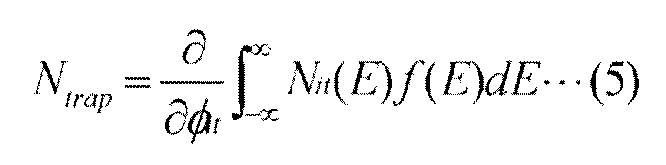
ここで、f(E)はフェルミ分布関数である。式(4)から得られたNtrapを式(5)でフィッティングすることで、Nitは決定される。このNitを設定したデバイスシミュレータを用いた計算により、Id<0.1pAを含む伝達特性を得ることができる。
次に、図17に示す実測のId−Vg特性に式(4)を適用し、Ntrapを抽出した結果を図19に白丸印で示す。ここで、図19の縦軸は半導体の伝導帯下端EcからのフェルミエネルギーEfである。破線を見るとEcのすぐ下の位置に極大値となっている。式(5)のNitとして、式(6)のテール分布を仮定すると図19の破線のように非常に良くNtrapをフィッティングでき、フィッティングパラメータとして、伝導帯端のトラップ密度Nta=1.67×1013cm−2/eV、特性減衰エネルギーWta=0.105eVが得られた。

次に、得られた界面準位のフィッティング曲線をデバイスシミュレータを用いた計算にフィードバックすることにより、Id−Vg特性を逆算した結果を図20A及び20Bに示す。図20Aに、ドレイン電圧Vdが0.1Vおよび1.8Vの場合の計算によって得られたId−Vg特性と、ドレイン電圧Vdが0.1V及び1.8Vの場合のトランジスタにおける実測のId−Vg特性とを示す。また、図20Bは、図20Aのドレイン電流Idを対数としたグラフである。
計算により得られた曲線と、実測値のプロットはほぼ一致しており、計算値と実測値とで高い再現性を有することが分かる。したがって、浅い欠陥準位密度を算出する方法として、上記の方法が十分に妥当であることが分かる。
[浅い欠陥準位密度の評価結果]
次に、上述の方法に基づいて、測定した電気特性と理想的な計算値とを比較することによって、二組の試料C1乃至C3の浅い欠陥準位密度を測定した。
次に、上述の方法に基づいて、測定した電気特性と理想的な計算値とを比較することによって、二組の試料C1乃至C3の浅い欠陥準位密度を測定した。
図21に二組の試料C1乃至C3の浅い欠陥準位密度の平均値を算出した結果を示す。試料C1乃至C3のいずれの試料においても、浅い欠陥準位密度のピーク値が、2.5×1012cm−2eV−1未満となり、浅い欠陥準位密度が極めて低い試料であることがわかる。なお、金属酸化物膜中の浅い欠陥準位密度のピーク値としては、2.5×1012cm−2eV−1未満、好ましくは1.75×1012cm−2eV−1未満、より好ましくは1.5×1012cm−2eV−1未満、さらに好ましくは7.5×1011cm−2eV−1未満である。
このように、試料C1乃至C3において、欠陥準位密度が低い金属酸化物膜が形成されたトランジスタであることが分かる。これは、低温かつ低酸素流量の条件で成膜した金属酸化物膜とすることで酸素透過性が向上し、トランジスタの作製工程中に拡散する酸素量が増大することにより、金属酸化物膜中、及び金属酸化物膜と絶縁膜との界面の酸素欠損等の欠陥が低減しているためだと示唆される。
<1−6.CPMによる金属酸化物膜中の深い欠陥準位の評価>
以下では、一定電流測定法(CPM:Constant Photocurrent Method)により、金属酸化物膜中の深い欠陥準位(以下、dDOSとも記す)について評価を行った。
以下では、一定電流測定法(CPM:Constant Photocurrent Method)により、金属酸化物膜中の深い欠陥準位(以下、dDOSとも記す)について評価を行った。
CPM測定は、試料に設けられた2電極間に電圧を印加した状態で光電流値が一定となるように端子間の試料面に照射する光量を調整し、照射する光量から吸収係数を導出することを各波長にて行うものである。CPM測定において、試料に欠陥があるとき、欠陥の存在する準位に応じたエネルギー(波長より換算)における吸収係数が増加する。この吸収係数の増加分に定数を掛けることにより、試料のdDOSを導出することができる。
CPM測定によって得られた吸収係数のカーブからバンドの裾に起因するアーバックテールと呼ばれる吸収係数分を取り除くことにより、欠陥準位による吸収係数を以下の式から算出することができる。なお、α(E)は、各エネルギーにおける吸収係数を表し、αuは、アーバックテールによる吸収係数を表す。

[CPM評価用の試料の作製]
以下では、3つの試料(試料D1乃至D3)を作製してCPM評価を行った。
以下では、3つの試料(試料D1乃至D3)を作製してCPM評価を行った。
まず、ガラス基板上に金属酸化物膜を成膜した。試料D1では、上記試料A1と同様の方法により厚さ約100nmの金属酸化物膜を成膜した。試料D2では、上記試料A2と同様の方法により、厚さ約100nmの金属酸化物膜を成膜した。試料D3では、上記試料A3と同様の方法により、厚さ約100nmの金属酸化物膜を成膜した。
続いて、金属酸化物膜上に、厚さ約30nmの酸化窒化シリコン膜、厚さ約100nmの酸化窒化シリコン膜、厚さ約20nmの酸化窒化シリコン膜を、プラズマCVD法により積層して形成した。
その後、窒素雰囲気下で350℃、1時間の熱処理を行った。
続いて、厚さ100nmの酸化物半導体膜を形成した。なお、当該酸化物半導体膜としては、2層の積層構造とした。1層目の酸化物半導体膜は、基板温度を170℃として、流量200sccmの酸素ガスをスパッタリング装置のチャンバー内に導入し、圧力を0.6Paとし、インジウムと、ガリウムと、亜鉛とを有する金属酸化物ターゲット(In:Ga:Zn=4:2:4.1[原子数比])に、2.5kWの交流電力を印加する条件下で、膜厚が10nmになるように形成した。2層目の酸化物半導体膜は、基板温度を170℃として、流量180sccmのアルゴンガスと、流量20sccmの酸素ガスとをスパッタリング装置のチャンバー内に導入し、圧力を0.6Paとし、インジウムと、ガリウムと、亜鉛とを有する金属酸化物ターゲット(In:Ga:Zn=4:2:4.1[原子数比])に、2.5kWの交流電力を印加する条件下で、膜厚が90nmになるように形成した。
その後、窒素と酸素との混合ガス雰囲気下で、350℃、1時間の熱処理を行った。
その後、酸化物半導体膜をウエットエッチング法によりエッチングして除去した。
続いて、酸化窒化シリコン膜を成膜した。酸化窒化シリコン膜は、成膜ガスとして流量160sccmのSiH4と、流量4000sccmのN2Oの混合ガスを用い、圧力200Pa、電力1500W、基板温度220℃の条件で、プラズマCVD法により成膜した。酸化窒化シリコン膜の厚さは約400nmである。
続いて、酸化窒化シリコン膜にフォトリソグラフィ法により開口部を形成した。
続いて、スパッタリング法により厚さ約50nmのTi膜、厚さ約400nmのAl膜、及び厚さ約100nmのTi膜の積層膜を成膜した。その後、積層膜をフォトリソグラフィ法により加工し、電極を形成した。
その後、窒素雰囲気下で250℃、1時間の熱処理を行った。
以上の工程により試料D1乃至D3を作製した。
[CPM評価結果]
図22に試料D1のCPM測定結果を、図23に試料D2のCPM測定結果を、図24に試料D3のCPM測定結果を、それぞれ示す。図22、図23、及び図24において、縦軸は吸収係数を表し、横軸は光エネルギーを表す。また図22、図23、及び図24において、黒い実線は、各試料の吸収係数のカーブを示し、点線は接線を示し、灰色の実線は光学的に測定した吸収係数を示す。
図22に試料D1のCPM測定結果を、図23に試料D2のCPM測定結果を、図24に試料D3のCPM測定結果を、それぞれ示す。図22、図23、及び図24において、縦軸は吸収係数を表し、横軸は光エネルギーを表す。また図22、図23、及び図24において、黒い実線は、各試料の吸収係数のカーブを示し、点線は接線を示し、灰色の実線は光学的に測定した吸収係数を示す。
図22から見積もった試料D1のアーバックテールの値は、68.70meVであり、吸収係数のカーブからアーバックテール起因の吸収係数を除いた吸収係数、すなわち深い欠陥準位に起因する吸収係数の値は、1.21×10⁻³cm−1であった。また、図23から見積もった試料D2のアーバックテールの値は、64.46meVであり、深い欠陥準位に起因する吸収係数の値は、1.36×10⁻³cm−1であった。また、図24から見積もった試料D3のアーバックテールの値は、65.83meVであり、深い欠陥準位に起因する吸収係数の値は、1.04×10⁻³cm−1であった。
以上の結果から、試料D1乃至D3に用いた金属酸化物膜は、深い欠陥準位に明確な差が見られていないことが分かる。試料D1乃至D3の深い欠陥準位に差が見られていない要因としては、金属酸化物膜に接して酸化物絶縁膜を形成し、当該酸化物絶縁膜から金属酸化物膜に十分な酸素供給が行われたことで、金属酸化物膜中の酸素欠損が補填されたためだと示唆される。
<1−7.金属酸化物膜の成膜方法>
以下では、本発明の一態様の金属酸化物膜の成膜方法について説明する。
以下では、本発明の一態様の金属酸化物膜の成膜方法について説明する。
本発明の一態様の金属酸化物膜は、酸素を含む雰囲気下にてスパッタリング法によって成膜することができる。
成膜時の基板温度は、室温以上150℃以下、好ましくは50℃以上150℃以下、より好ましくは100℃以上150℃以下、代表的には130℃の温度とすることが好ましい。基板温度を上述の範囲とすることで、配向性を有する結晶部と、配向性を有さない結晶部との存在割合を制御することができる。
また、成膜時の酸素の流量比(酸素分圧)を、0%以上50%未満、好ましくは0%以上30%以下、より好ましくは0%以上20%以下、さらに好ましくは0%以上15%以下、代表的には10%とすることが好ましい。酸素流量を低減することにより、配向性を有さない結晶部をより多く膜中に含ませることができる。
したがって、成膜時の基板温度と、成膜時の酸素流量を上述の範囲とすることで、配向性を有する結晶部と、配向性を有さない結晶部とが混在した金属酸化物膜を得ることができる。また、基板温度と酸素流量を上述の範囲内とすることにより、配向性を有する結晶部と配向性を有さない結晶部の存在割合を制御することが可能となる。
金属酸化物膜の成膜に用いることの可能な酸化物ターゲットとしては、In−Ga−Zn系酸化物に限られず、例えば、In−M−Zn系酸化物(Mは、Al、Ga、Y、またはSn)を適用することができる。
また、複数の結晶粒を有する多結晶酸化物を含むスパッタリングターゲットを用いて、結晶部を含む金属酸化物膜を成膜すると、多結晶酸化物を含まないスパッタリングターゲットを用いた場合に比べて、結晶性を有する金属酸化物膜が得られやすい。
以下に、金属酸化物膜の成膜メカニズムにおける一考察について、図25A乃至25Dを用いて説明する。スパッタリング用ターゲットが複数の結晶粒を有し、且つ、その結晶粒が層状構造を有しており、当該結晶粒に劈開しやすい界面が存在する場合、当該スパッタリング用ターゲットにイオンを衝突させることで、結晶粒が劈開する。ここで、スパッタリング用ターゲットは、例えば、後述する図27のように、Inと、M(MはAl、Ga、Y、またはSn)と、Znと、を含む、c軸方向に配向した層状の構造を有するものとする。なお、当該結晶粒は、平板状又はペレット状のクラスターであり、ナノクラスターまたはペレットと呼ぶこともできる。
ここで、図25Aに示すように、ターゲットから劈開したナノクラスター20は、平板状であるため、平面側を基板32の表面に向けて堆積しやすい。なお、後述する図27のように、Inと、M(MはAl、Ga、Y、またはSn)と、Znと、を含む、c軸方向に配向した層状の構造を有する場合、図27に示す(M,Zn)層と(M,Zn)層の界面で劈開しやすい。
次に、ターゲットからはじき出された粒子23が基板32の表面に達する。粒子23は、原子1個または原子数個の集合体を有する。そのため、粒子23を原子状粒子(atomic particles)と呼ぶこともできる。ここで、ナノクラスターが後述する図27のような、Inと、M(MはAl、Ga、Y、またはSn)と、Znと、を含む、c軸方向に配向した層状の構造を有する場合、粒子23は、ナノクラスター20の上面より側面に結合しやすい。よって、粒子23は、ナノクラスター20の形成されていない領域を埋めるように、ナノクラスター20の側面に優先的に付着する。粒子23は、結合手が活性状態となることで、ナノクラスター20と化学的に連結して横成長部22を形成する(図25A参照。)。粒子23は、ナノクラスター20とナノクラスター20の間の領域に入り込むということもできる。
横成長部22は、ナノクラスター20とナノクラスター20の間の領域26(領域26は、Lateral Growth Buffer Region(LGBR)と呼称することもできる。)を埋めるように横方向に成長(ラテラル成長ともいう。)する。ここで、横方向とは、例えばナノクラスター20中のc軸に垂直な方向を指す。
ここで、450℃以下、好ましくは400℃以下程度の基板加熱により、ナノクラスター20の横成長部22に粒子23が付着し、粒子23にLGBRを介して拡散した酸素が付着し、再び粒子23が同様に付着する、という反応が起きやすくなる。この繰り返しにより横方向の固相成長が起きていると推定される。このようなナノクラスターの横方向の成長を自己組織化と呼ぶこともできる。
さらに横成長部22がラテラル成長することで、横成長部22が互いに衝突する。横成長部22が衝突した部分を連結部27として隣接するナノクラスター20が連結される(図25B参照。)。つまり、領域26中に連結部27が形成される。これは、粒子23が、ナノクラスター20の側面に横成長部22を形成し、横成長部22が横方向に成長することで、ナノクラスター20間の領域26を充填しているということもできる。このように、ナノクラスター20の形成されていない領域を埋めるまで横成長部22が形成される。
したがって、ナノクラスター20がそれぞれ異なる方向を向けて形成される場合でも、ナノクラスター20とナノクラスター20の隙間を粒子23がラテラル成長しながら埋めるため、明確な結晶粒界が形成されることがない。
ここで、ナノクラスター20間を、粒子23が滑らかに連結(アンカリング)するため、連結部27において単結晶とも多結晶とも異なる結晶構造が形成される。言い換えると、ナノクラスター20の間の連結部27に歪みを有する結晶構造が形成される。これにより、例えば、連結部27において、上面の形状が六角形だった結晶構造が変形し、五角形または七角形になる場合もある。
次に、新たなナノクラスター20が、平面側を基板32の表面に向けて形成される。そして、粒子23が、ナノクラスター20の形成されていない領域を埋めるように堆積することで横成長部22を形成する(図25C参照。)。こうして、粒子23がナノクラスター20の側面に付着し、横成長部22がラテラル成長することで、二層目のナノクラスター20間を連結させる(図25D参照。)。m層目(mは二以上の整数。)が形成されるまで成膜は続き、積層体を有する金属酸化物膜が形成される。
また、基板32を加熱することにより、基板表面においてナノクラスター20同士の結合、または再配列が進むことにより、配向性を有する結晶部を含む金属酸化物膜が形成されやすくなると考えられる。
なお、本実施の形態で説明したように、スパッタリング法を用いて、金属酸化物膜を形成すると、結晶性の制御が容易であるため好ましい。ただし、本発明の一態様の金属酸化物膜の形成方法としては、これに限定されず、例えばパルスレーザー堆積(PLD)法、プラズマ化学気相堆積(PECVD)法、熱CVD(Chemical Vapor Deposition)法、ALD(Atomic Layer Deposition)法、真空蒸着法などを用いてもよい。熱CVD法の例としては、MOCVD(Metal Organic Chemical Vapor Deposition)法が挙げられる。
<1−8.金属酸化物膜の組成及び構造について>
本発明の一態様の金属酸化物膜をトランジスタなどの半導体装置に適用することができる。以下では、特に半導体特性を有する金属酸化物膜(以下では酸化物半導体膜と呼ぶ)について説明する。
本発明の一態様の金属酸化物膜をトランジスタなどの半導体装置に適用することができる。以下では、特に半導体特性を有する金属酸化物膜(以下では酸化物半導体膜と呼ぶ)について説明する。
まず、酸化物半導体膜の組成について説明する。
酸化物半導体膜は、先の記載のように、インジウム(In)と、M(MはAl、Ga、Y、またはSnを表す。)と、Zn(亜鉛)と、を有する。
なお、元素Mは、アルミニウム、ガリウム、イットリウムまたはスズとするが、元素Mに適用可能な元素としては、上記以外にも、ホウ素、シリコン、チタン、鉄、ニッケル、ゲルマニウム、ジルコニウム、モリブデン、ランタン、セリウム、ネオジム、ハフニウム、タンタル、タングステン、マグネシウムなどを用いてもよい。また、元素Mとして、前述の元素を複数組み合わせても構わない。
次に、本発明の一態様に係る酸化物半導体膜が有するインジウム、元素M及び亜鉛の原子数比の好ましい範囲について、図26A乃至26Cを用いて説明する。なお、図26A乃至26Cには、酸素の原子数比については記載しない。また、酸化物半導体膜が有するインジウム、元素M、及び亜鉛の原子数比のそれぞれの項を[In]、[M]、及び[Zn]とする。
図26A乃至26Cにおいて、破線は、[In]:[M]:[Zn]=(1+α):(1−α):1の原子数比(−1≦α≦1)となるライン、[In]:[M]:[Zn]=(1+α):(1−α):2の原子数比となるライン、[In]:[M]:[Zn]=(1+α):(1−α):3の原子数比となるライン、[In]:[M]:[Zn]=(1+α):(1−α):4の原子数比となるライン、及び[In]:[M]:[Zn]=(1+α):(1−α):5の原子数比となるラインを表す。
また、一点鎖線は、[In]:[M]:[Zn]=1:1:βの原子数比(β≧0)となるライン、[In]:[M]:[Zn]=1:2:βの原子数比となるライン、[In]:[M]:[Zn]=1:3:βの原子数比となるライン、[In]:[M]:[Zn]=1:4:βの原子数比となるライン、[In]:[M]:[Zn]=2:1:βの原子数比となるライン、及び[In]:[M]:[Zn]=5:1:βの原子数比となるラインを表す。
また、図26A乃至26Cに示す、[In]:[M]:[Zn]=0:2:1の原子数比またはその近傍値の酸化物半導体膜は、スピネル型の結晶構造をとりやすい。
図26A及び26Bでは、本発明の一態様の酸化物半導体膜が有する、インジウム、元素M、及び亜鉛の原子数比の好ましい範囲の一例について示している。
一例として、図27に、[In]:[M]:[Zn]=1:1:1である、InMZnO4の結晶構造を示す。また、図27は、b軸に平行な方向から観察した場合のInMZnO4の結晶構造である。なお、図27に示すM、Zn、酸素を有する層(以下、(M,Zn)層)における金属元素は、元素Mまたは亜鉛を表している。この場合、元素Mと亜鉛の割合が等しいものとする。元素Mと亜鉛とは、置換が可能であり、配列は不規則である。
また、インジウムと元素Mは、互いに置換可能である。そのため、(M,Zn)層の元素Mがインジウムと置換し、(In,M,Zn)層と表すこともできる。その場合、In層が1に対し、(In,M,Zn)層が2である層状構造をとる。
また、インジウムと元素Mは、互いに置換可能である。そのため、MZnO2層の元素Mがインジウムと置換し、InαM1−αZnO2層(0<α≦1)と表すこともできる。その場合、InO2層が1に対し、InαM1−αZnO2層が2である層状構造をとる。また、InO2層のインジウムが元素Mと置換し、In1−αMαO2層(0<α≦1)と表すこともできる。その場合、In1−αMαO2層が1に対し、MZnO2層が2である層状構造をとる。
[In]:[M]:[Zn]=1:1:2となる原子数比の酸化物は、In層が1に対し、(M,Zn)層が3である層状構造をとる。つまり、[In]および[M]に対し[Zn]が大きくなると、酸化物が結晶化した場合、In層に対する(M,Zn)層の割合が増加する。
ただし、酸化物中において、In層が1に対し、(M,Zn)層が非整数である場合、In層が1に対し、(M,Zn)層が整数である層状構造を複数種有する場合がある。例えば、[In]:[M]:[Zn]=1:1:1.5である場合、In層が1に対し、(M,Zn)層が2である層状構造と、(M,Zn)層が3である層状構造とが混在する層状構造となる場合がある。
例えば、酸化物半導体膜をスパッタリング装置にて成膜する場合、ターゲットの原子数比からずれた原子数比の膜が形成される。特に、成膜時の基板温度によっては、ターゲットの[Zn]よりも、膜の[Zn]が小さくなる場合がある。
また、酸化物半導体膜中に複数の相が共存する場合がある(二相共存、三相共存など)。例えば、[In]:[M]:[Zn]=0:2:1の原子数比、及びその近傍値である原子数比では、スピネル型の結晶構造と層状の結晶構造との二相が共存しやすい。また、[In]:[M]:[Zn]=1:0:0を示す原子数比、及びその近傍値である原子数比では、ビックスバイト型の結晶構造と層状の結晶構造との二相が共存しやすい。酸化物半導体膜中に複数の相が共存する場合、異なる結晶構造の間において、粒界(グレインバウンダリーともいう)が形成される場合がある。
また、インジウムの含有率を高くすることで、酸化物半導体膜のキャリア移動度(電子移動度)を高くすることができる。これは、インジウム、元素M及び亜鉛を有する酸化物半導体膜では、主として重金属のs軌道がキャリア伝導に寄与しており、インジウムの含有率を高くすることにより、s軌道が重なる領域がより大きくなるため、インジウムの含有率が高い酸化物半導体膜はインジウムの含有率が低い酸化物半導体膜と比較してキャリア移動度が高くなるためである。
一方、酸化物半導体膜中のインジウム及び亜鉛の含有率が低くなると、キャリア移動度が低くなる。従って、[In]:[M]:[Zn]=0:1:0を示す原子数比、及びその近傍値である原子数比(例えば図26Cに示す領域C)では、絶縁性が高くなる。
従って、本発明の一態様の酸化物半導体膜は、キャリア移動度が高く、かつ、粒界が少ない層状構造となりやすい、図26Aの領域Aで示される原子数比を有することが好ましい。
また、図26Bに示す領域Bは、[In]:[M]:[Zn]=4:2:3から4.1、及びその近傍値を示している。近傍値には、例えば、原子数比が[In]:[M]:[Zn]=5:3:4が含まれる。領域Bで示される原子数比を有する酸化物半導体膜は、特に、結晶性が高く、キャリア移動度も高い優れた酸化物半導体膜である。
なお、酸化物半導体膜が、層状構造を形成する条件は、原子数比によって一義的に定まらない。原子数比により、層状構造を形成するための難易の差はある。一方、同じ原子数比であっても、形成条件により、層状構造になる場合も層状構造にならない場合もある。従って、図示する領域は、酸化物半導体膜が層状構造を有する原子数比を示す領域であり、領域A乃至Cの境界は厳密ではない。
<1−9.金属酸化物膜の構造>
次に、金属酸化物膜(以下では酸化物半導体と呼ぶ)の構造について説明する。
次に、金属酸化物膜(以下では酸化物半導体と呼ぶ)の構造について説明する。
酸化物半導体は、単結晶酸化物半導体と、それ以外の非単結晶酸化物半導体と、に分けられる。非単結晶酸化物半導体としては、CAAC−OS(c−axis−aligned crystalline oxide semiconductor)、多結晶酸化物半導体、nc−OS(nanocrystalline oxide semiconductor)、擬似非晶質酸化物半導体(a−like OS:amorphous−like oxide semiconductor)及び非晶質酸化物半導体などがある。
また別の観点では、酸化物半導体は、非晶質酸化物半導体と、それ以外の結晶性酸化物半導体と、に分けられる。結晶性酸化物半導体としては、単結晶酸化物半導体、CAAC−OS、多結晶酸化物半導体及びnc−OSなどがある。
非晶質構造は、一般に、等方的であって不均質構造を持たない、準安定状態で原子の配置が固定化していない、結合角度が柔軟である、短距離秩序は有するが長距離秩序を有さない、などといわれている。
すなわち、安定な酸化物半導体を完全な非晶質(completely amorphous)酸化物半導体とは呼べない。また、等方的でない(例えば、微小な領域において周期構造を有する)酸化物半導体を、完全な非晶質酸化物半導体とは呼べない。一方、a−like OSは、等方的でないが、鬆(ボイドともいう。)を有する不安定な構造である。不安定であるという点では、a−like OSは、物性的に非晶質酸化物半導体に近い。
[CAAC−OS]
まずは、CAAC−OSについて説明する。
まずは、CAAC−OSについて説明する。
CAAC−OSは、c軸配向した複数の結晶部(ペレットともいう。)を有する酸化物半導体の一種である。
CAAC−OSは結晶性の高い酸化物半導体である。酸化物半導体の結晶性は不純物の混入や欠陥の生成などによって低下する場合があるため、CAAC−OSは不純物や欠陥(酸素欠損など)の少ない酸化物半導体ともいえる。
なお、不純物は、酸化物半導体の主成分以外の元素で、水素、炭素、シリコン、遷移金属元素などがある。例えば、シリコンなどの、酸化物半導体を構成する金属元素よりも酸素との結合力の強い元素は、酸化物半導体から酸素を奪うことで酸化物半導体の原子配列を乱し、結晶性を低下させる要因となる。また、鉄やニッケルなどの重金属、アルゴン、二酸化炭素などは、原子半径(または分子半径)が大きいため、酸化物半導体の原子配列を乱し、結晶性を低下させる要因となる。
[nc−OS]
次に、nc−OSについて説明する。
次に、nc−OSについて説明する。
nc−OSをXRDによって解析した場合について説明する。例えば、nc−OSに対し、out−of−plane法による構造解析を行うと、配向性を示すピークが現れない。即ち、nc−OSの結晶は配向性を有さない。
nc−OSは、非晶質酸化物半導体よりも規則性の高い酸化物半導体である。そのため、nc−OSは、a−like OSや非晶質酸化物半導体よりも欠陥準位密度が低くなる。ただし、nc−OSは、異なるペレット間で結晶方位に規則性が見られない。そのため、nc−OSは、CAAC−OSと比べて欠陥準位密度が高くなる場合がある。
[a−like OS]
a−like OSは、nc−OSと非晶質酸化物半導体との間の構造を有する酸化物半導体である。
a−like OSは、nc−OSと非晶質酸化物半導体との間の構造を有する酸化物半導体である。
a−like OSは、鬆または低密度領域を有する。a−like OSは、鬆を有するため、不安定な構造である。
また、a−like OSは、鬆を有するため、nc−OS及びCAAC−OSと比べて密度の低い構造である。具体的には、a−like OSの密度は、同じ組成の単結晶の密度の78.6%以上92.3%未満である。また、nc−OSの密度及びCAAC−OSの密度は、同じ組成の単結晶の密度の92.3%以上100%未満である。単結晶の密度の78%未満である酸化物半導体は、成膜すること自体が困難である。
例えば、In:Ga:Zn=1:1:1[原子数比]を満たす酸化物半導体において、菱面体晶構造を有する単結晶InGaZnO4の密度は6.357g/cm3である。よって、例えば、In:Ga:Zn=1:1:1[原子数比]を満たす酸化物半導体において、a−like OSの密度は5.0g/cm3以上5.9g/cm3未満である。また、例えば、In:Ga:Zn=1:1:1[原子数比]を満たす酸化物半導体において、nc−OSの密度及びCAAC−OSの密度は5.9g/cm3以上6.3g/cm3未満である。
なお、同じ組成の単結晶が存在しない場合、任意の割合で組成の異なる単結晶を組み合わせることにより、所望の組成における単結晶に相当する密度を見積もることができる。所望の組成の単結晶に相当する密度は、組成の異なる単結晶を組み合わせる割合に対して、加重平均を用いて見積もればよい。ただし、密度は、可能な限り少ない種類の単結晶を組み合わせて見積もることが好ましい。
以上のように、酸化物半導体は、様々な構造をとり、それぞれが様々な特性を有する。なお、酸化物半導体は、例えば、非晶質酸化物半導体、a−like OS、nc−OS、CAAC−OSのうち、二種以上を有する積層膜であってもよい。
<1−10.金属酸化物膜をトランジスタに用いる構成>
続いて、金属酸化物膜(以下では酸化物半導体膜と呼ぶ)をトランジスタに用いる構成について説明する。
続いて、金属酸化物膜(以下では酸化物半導体膜と呼ぶ)をトランジスタに用いる構成について説明する。
なお、酸化物半導体膜をトランジスタに用いることで、例えば、多結晶シリコンをチャネル領域に用いたトランジスタと比較し、結晶粒界におけるキャリア散乱等を減少させることができるため、高い電界効果移動度のトランジスタを実現することができる。また、信頼性の高いトランジスタを実現することができる。
本発明の一態様の酸化物半導体膜は、配向性を有する結晶部と、配向性を有さない結晶部とが混在している膜である。このような結晶性を有する酸化物半導体膜を用いることで、高い電界効果移動度と、高い信頼性を両立したトランジスタを実現することができる。
<1−11.金属酸化物膜のキャリア密度>
金属酸化物膜(以下では酸化物半導体膜)のキャリア密度について、以下に説明を行う。
金属酸化物膜(以下では酸化物半導体膜)のキャリア密度について、以下に説明を行う。
酸化物半導体膜のキャリア密度に影響を与える因子としては、酸化物半導体膜中の酸素欠損(Vo)、または酸化物半導体膜中の不純物などが挙げられる。
酸化物半導体膜中の酸素欠損が多くなると、該酸素欠損に水素が結合(この状態をVoHともいう)した際に、欠陥準位密度が高くなる。または、酸化物半導体膜中の不純物が多くなると、該不純物に起因し欠陥準位密度が高くなる。したがって、酸化物半導体膜中の欠陥準位密度を制御することで、酸化物半導体膜のキャリア密度を制御することができる。
ここで、酸化物半導体膜をチャネル領域に用いるトランジスタを考える。
トランジスタのしきい値電圧のマイナスシフトの抑制、またはトランジスタのオフ電流の低減を目的とする場合においては、酸化物半導体膜のキャリア密度を低くする方が好ましい。酸化物半導体膜のキャリア密度を低くする場合においては、酸化物半導体膜中の不純物濃度を低くし、欠陥準位密度を低くすればよい。本明細書等において、不純物濃度が低く、欠陥準位密度の低いことを高純度真性または実質的に高純度真性と言う。高純度真性の酸化物半導体膜のキャリア密度としては、8×1015cm−3未満、好ましくは1×1011cm−3未満、さらに好ましくは1×1010cm−3未満であり、1×10⁻⁹cm−3以上とすればよい。
一方で、トランジスタのオン電流の向上、またはトランジスタの電界効果移動度の向上を目的とする場合においては、酸化物半導体膜のキャリア密度を高くする方が好ましい。酸化物半導体膜のキャリア密度を高くする場合においては、酸化物半導体膜の不純物濃度をわずかに高める、または酸化物半導体膜の欠陥準位密度をわずかに高めればよい。あるいは、酸化物半導体膜のバンドギャップをより小さくするとよい。例えば、トランジスタのId−Vg特性のオン/オフ比が取れる範囲において、不純物濃度がわずかに高い、または欠陥準位密度がわずかに高い酸化物半導体膜は、実質的に真性とみなせる。また、電子親和力が大きく、それにともなってバンドギャップが小さくなり、その結果、熱励起された電子(キャリア)の密度が増加した酸化物半導体膜は、実質的に真性とみなせる。なお、より電子親和力が大きな酸化物半導体膜を用いた場合には、トランジスタのしきい値電圧がより低くなる。
上述のキャリア密度が高められた酸化物半導体膜は、わずかにn型化している。したがって、キャリア密度が高められた酸化物半導体膜を、「Slightly−n」と呼称してもよい。
実質的に真性の酸化物半導体膜のキャリア密度は、1×105cm−3以上1×1018cm−3未満が好ましく、1×107cm−3以上1×1017cm−3以下がより好ましく、1×109cm−3以上5×1016cm−3以下がさらに好ましく、1×1010cm−3以上1×1016cm−3以下がさらに好ましく、1×1011cm−3以上1×1015cm−3以下がさらに好ましい。
また、上述の実質的に真性の酸化物半導体膜を用いることで、トランジスタの信頼性が向上する場合がある。ここで、図28を用いて、酸化物半導体膜をチャネル領域に用いるトランジスタの信頼性が向上する理由について説明する。図28は、酸化物半導体膜をチャネル領域に用いるトランジスタにおけるエネルギーバンドを説明する図である。
図28において、GEはゲート電極を、GIはゲート絶縁膜を、OSは酸化物半導体膜を、SDはソース電極またはドレイン電極を、それぞれ表す。すなわち、図28は、ゲート電極と、ゲート絶縁膜と、酸化物半導体膜と、酸化物半導体膜に接するソース電極またはドレイン電極のエネルギーバンドの一例である。
また、図28において、ゲート絶縁膜としては、酸化シリコン膜を用い、酸化物半導体膜にIn−Ga−Zn酸化物を用いる構成である。また、酸化シリコン膜中に形成されうる欠陥の遷移レベル(εf)はゲート絶縁膜の伝導帯から3.1eV離れた位置に形成されるものとし、ゲート電圧(Vg)が30Vの場合の酸化物半導体膜と酸化シリコン膜との界面における酸化シリコン膜のフェルミ準位(Ef)をゲート絶縁膜の伝導帯から3.6eVとする。なお、酸化シリコン膜のフェルミ準位は、ゲート電圧に依存し変動する。例えば、ゲート電圧を大きくすることで、酸化物半導体膜と、酸化シリコン膜との界面における酸化シリコン膜のフェルミ準位(Ef)は低くなる。また、図28中の白丸は電子(キャリア)を表し、図28中のXは酸化シリコン膜中の欠陥準位を表す。
図28に示すように、ゲート電圧が印加された状態で、例えばキャリアが熱励起されると、欠陥準位(図中X)にキャリアがトラップされ、プラス(“+”)からニュートラル(“0”)に欠陥準位の荷電状態が変化する。すなわち、酸化シリコン膜のフェルミ準位(Ef)に上述の熱励起のエネルギーを足した値が欠陥の遷移レベル(εf)よりも高くなる場合、酸化シリコン膜中の欠陥準位の荷電状態は正の状態から中性となり、トランジスタのしきい値電圧がプラス方向に変動することになる。
また、電子親和力が異なる酸化物半導体膜を用いると、ゲート絶縁膜と酸化物半導体膜との界面のフェルミ準位が形成される深さが異なることがある。電子親和力の大きな酸化物半導体膜を用いると、ゲート絶縁膜と酸化物半導体膜との界面及びその近傍において、ゲート絶縁膜の伝導帯が上方に移動する。この場合、ゲート絶縁膜中に形成されうる欠陥準位(図28中X)も上方に移動するため、ゲート絶縁膜と酸化物半導体膜との界面のフェルミ準位とのエネルギー差が大きくなる。該エネルギー差が大きくなることにより、ゲート絶縁膜中にトラップされる電荷が少なくなる、例えば、上述の酸化シリコン膜中に形成されうる欠陥準位の荷電状態の変化が少なくなり、ゲートバイアス熱(Gate Bias Temperature:GBTともいう)ストレスにおける、トランジスタのしきい値電圧の変動を小さくできる。
また、酸化物半導体膜の欠陥準位に捕獲された電荷は、消失するまでに要する時間が長く、あたかも固定電荷のように振る舞うことがある。そのため、欠陥準位密度の高い酸化物半導体膜にチャネル領域が形成されるトランジスタは、電気特性が不安定となる場合がある。
従って、トランジスタの電気特性を安定にするためには、酸化物半導体膜中の不純物濃度を低減することが有効である。また、酸化物半導体膜中の不純物濃度を低減するためには、近接する膜中の不純物濃度も低減することが好ましい。不純物としては、水素、窒素、アルカリ金属、アルカリ土類金属、鉄、ニッケル、シリコン等がある。
ここで、酸化物半導体膜中における各不純物の影響について説明する。
酸化物半導体膜において、第14族元素の一つであるシリコンや炭素が含まれると、酸化物半導体膜において欠陥準位が形成される。このため、酸化物半導体膜におけるシリコンや炭素の濃度と、酸化物半導体膜の界面及びその近傍のシリコンや炭素の濃度(二次イオン質量分析法(SIMS:Secondary Ion Mass Spectrometry)により得られる濃度)を、2×10¹⁸atoms/cm3以下、好ましくは2×1017atoms/cm3以下とする。
また、酸化物半導体膜にアルカリ金属またはアルカリ土類金属が含まれると、欠陥準位を形成し、キャリアを生成する場合がある。従って、アルカリ金属またはアルカリ土類金属が含まれている酸化物半導体膜を用いたトランジスタはノーマリーオンとなりやすい。このため、酸化物半導体膜中のアルカリ金属またはアルカリ土類金属の濃度を低減することが好ましい。具体的には、SIMSにより得られる酸化物半導体膜中のアルカリ金属またはアルカリ土類金属の濃度を、1×10¹⁸atoms/cm3以下、好ましくは2×1016atoms/cm3以下にする。
また、酸化物半導体膜において、窒素が含まれると、キャリアである電子が生じ、キャリア密度が増加し、n型になりやすい。この結果、窒素が含まれている酸化物半導体膜を半導体に用いたトランジスタはノーマリーオンとなりやすい。従って、該酸化物半導体膜において、窒素はできる限り低減されていることが好ましく、例えば、SIMSにより得られる酸化物半導体膜中の窒素濃度は、5×10¹⁹atoms/cm3未満、好ましくは5×1018atoms/cm3以下、より好ましくは1×1018atoms/cm3以下、さらに好ましくは5×1017atoms/cm3以下とする。
また、酸化物半導体膜に含まれる水素は、金属原子と結合する酸素と反応して水になるため、酸素欠損を形成する場合がある。該酸素欠損に水素が入ることで、キャリアである電子が生成される場合がある。また、水素の一部が金属原子と結合する酸素と結合して、キャリアである電子を生成することがある。従って、水素が含まれている酸化物半導体膜を用いたトランジスタはノーマリーオンとなりやすい。このため、酸化物半導体膜中の水素はできる限り低減されていることが好ましい。具体的には、酸化物半導体膜において、SIMSにより得られる水素濃度を、1×10²⁰atoms/cm3未満、好ましくは1×1019atoms/cm3未満、より好ましくは5×1018atoms/cm3未満、さらに好ましくは1×1018atoms/cm3未満とする。
不純物が十分に低減された酸化物半導体膜をトランジスタのチャネル形成領域に用いることで、トランジスタに安定した電気特性を付与することができる。
また、酸化物半導体膜は、エネルギーギャップが2eV以上、または2.5eV以上であると好ましい。
また、酸化物半導体膜の厚さは、3nm以上200nm以下、好ましくは3nm以上100nm以下、さらに好ましくは3nm以上60nm以下である。
また、酸化物半導体膜がIn−M−Zn酸化物の場合、In−M−Zn酸化物を成膜するために用いるスパッタリングターゲットの金属元素の原子数比として、In:M:Zn=1:1:0.5、In:M:Zn=1:1:1、In:M:Zn=1:1:1.2、In:M:Zn=2:1:1.5、In:M:Zn=2:1:2.3、In:M:Zn=2:1:3、In:M:Zn=3:1:2、In:M:Zn=4:2:4.1、In:M:Zn=5:1:7等が好ましい。
<1−12.金属酸化物膜の酸素拡散>
金属酸化物膜(以下では酸化物半導体膜)への酸素拡散について、以下に説明を行う。
金属酸化物膜(以下では酸化物半導体膜)への酸素拡散について、以下に説明を行う。
上述の酸化物半導体膜に含まれるナノクラスターの構造を図29A及び29Bに示す。図29Aに示すナノクラスター(ペレットと呼ぶこともできる。)は、2つの(In,M,Zn)層(In,M(MはAl、Ga、Y、またはSn)、Zn、酸素を有する層)の間にIn層(In,酸素を有する層)が形成されている。また、図29Bに示すように、(In,M,Zn)層の代わりに(M,Zn)層(M、Zn、酸素を有する層)が形成される場合もある。
例えば、[In]:[M]:[Zn]=1:1:1である場合、図27に示す結晶構造のように、2つの(M,Zn)層の間にIn層が形成される場合が多い。また、例えば、[In]:[M]:[Zn]=4:2:3から4.1、及びその近傍値をとる場合のように、[In]:[M]:[Zn]=1:1:1よりもIn量が多い場合、図27に示す結晶構造の(M,Zn)層の元素MまたはZnの一部がInに置換されて、(In,M,Zn)層が形成される場合が多い。
また、複数のナノクラスターが膜の厚さ方向に配向性を有するように配列した結晶部が、上述のc軸配向性を有する結晶部である。また、複数のナノクラスターが膜の厚さ方向に配向性を有さず、様々な向きに配向する結晶部が、上述のc軸配向性を有さない結晶部である。
また、[In]:[M]:[Zn]=4:2:3から4.1、及びその近傍値をとる場合、比較的酸化亜鉛の含有量が多いので、酸化物半導体膜にc軸配向性を有する結晶部の存在割合が大きくなる。
上述の成膜方法を用いて酸化物半導体膜を成膜することにより、成膜時にナノクラスターに酸素欠損が形成されやすくなる。また、酸化物半導体膜中の、c軸配向性を有さない結晶部の存在割合が大きくなる条件(例えば、成膜温度を室温とし、酸素流量比を10%以下とする。)で成膜することにより、さらに成膜時にナノクラスターに酸素欠損が形成されやすくなる。酸素欠損は(In,M,Zn)層及びIn層に形成される。特に、(M,Zn)層のMまたはZnがInに置換された(In,M,Zn)層ではInの近傍に酸素欠損が形成されやすい。ここで、酸素欠損が形成されるということは、In,MまたはZnの間に存在していた酸素がなくなることである。よって、酸素欠損が形成されることにより、ナノクラスターを形成する(In,M,Zn)層及びIn層の結晶構造に歪みが生じる。
ここで、酸素欠損が形成された酸化物半導体膜に接して、十分な酸素供給源として機能する酸化物膜を形成することにより、当該酸化物膜から酸素を供給することができる。このような酸化物膜としては、過剰酸素を有する酸化物半導体膜または酸化物絶縁膜を用いればよい。酸化物半導体膜としては、例えば上記の金属酸化物膜を用いることができる。また、酸化物絶縁膜としては、例えば酸化シリコンまたは酸化窒化シリコンなどを用いることができる。なお、酸素供給源として機能する酸化物膜は、必ずしも酸化物半導体膜に接して形成する必要はない。例えば、酸素供給源として機能する酸化物膜と酸化物半導体膜の間に酸素透過性を有する膜を形成してもよい。
過剰酸素を有する酸化物半導体膜または酸化物絶縁膜を形成するには、例えば、成膜時の雰囲気を酸素過剰雰囲気(例えば、成膜ガスを酸素100%にする。)として成膜すればよい。また、例えば、酸化物半導体膜または酸化物絶縁膜に、イオン注入法、イオンドーピング法またはプラズマ処理によって酸素を添加すればよい。また、例えば、酸化物半導体膜または酸化物絶縁膜の上に、酸素を含む雰囲気でスパッタリング法を用いて成膜することによって、酸素を添加すればよい。
なお、酸素供給源として機能する酸化物膜から酸化物半導体膜に酸素を供給する際に、当該酸化物半導体膜に、過剰な水または水素などの不純物が含まれていると、酸化物半導体膜中の酸素の拡散が妨げられる場合がある。このため、酸素供給源として機能する酸化物膜を形成する前に、酸化物半導体膜に加熱処理を行って、脱水化、脱水素化を行うことが好ましい。
酸素供給源として機能する酸化物膜に接して酸化物半導体膜を形成し、加熱処理を行うことにより、当該酸化物膜から酸化物半導体膜に過剰酸素(活性酸素)を供給することができる。ここで、ナノクラスターには酸素欠損によって歪みが生じているため、活性酸素は酸素欠損による歪みを介して酸化物半導体膜の内部まで拡散する。
拡散した活性酸素は、ナノクラスターの表面または側面、例えば、(In,M,Zn)層に形成された酸素欠損を補填する。これにより、ナノクラスターの表面または側面において酸素欠損を低減し、(In,M,Zn)層に形成された酸素欠損に起因するsDOSを小さくすることができる。
ここで、ナノクラスターの表面または側面の酸素欠損が補填されることにより、活性酸素はナノクラスターの内部に侵入しにくくなる。さらに加熱処理によって酸化物半導体膜中の水素も拡散する。このため、水素がナノクラスター内部、例えばIn層に形成された酸素欠損にトラップされ、ナノクラスターの内部ではVoHが形成されやすくなる。VoHはキャリアを生成するため、ナノクラスター内部のキャリア密度が大きくなる。
このような酸化物半導体膜を用いてトランジスタを形成することによる、ナノクラスター内部のキャリア密度の増大により、当該トランジスタのオン電流を著しく上昇させることができる。さらに、ナノクラスター表面及び側面のsDOSを低減させることにより、当該トランジスタのサブスレッショルドスイング値を小さくすることができる。
また、酸化物半導体膜を用いたトランジスタでは、主にIn層で生成されたキャリアが(In,M,Zn)層または(M,Zn)層に形成される伝導帯の下端を主に流れると考えられる。このとき、伝導帯の下端は主にInOx(x>0)、ZnOx(x>0)によって形成されると推測される。
本実施の形態は、少なくともその一部を本明細書中に記載する他の実施の形態と適宜組み合わせて実施することができる。
(実施の形態2)
<CACの構成>
以下では、本発明の一態様に用いることができる金属酸化物膜(以下では酸化物半導体膜とも呼ぶ)としてCAC(Cloud Aligned Complementary)−OSの構成について説明する。
<CACの構成>
以下では、本発明の一態様に用いることができる金属酸化物膜(以下では酸化物半導体膜とも呼ぶ)としてCAC(Cloud Aligned Complementary)−OSの構成について説明する。
CACとは、例えば、酸化物半導体を構成する元素が、0.5nm以上10nm以下、好ましくは、1nm以上2nm以下、またはその近傍のサイズで偏在した材料の一構成である。なお、以下では、酸化物半導体において、一つあるいはそれ以上の金属元素が偏在し、該金属元素を有する領域が、0.5nm以上10nm以下、好ましくは、1nm以上2nm以下、またはその近傍のサイズで混合した状態をモザイク状、またはパッチ状ともいう。
例えば、In−Ga−Zn酸化物(以下、IGZOともいう。)におけるCAC−IGZOとは、インジウム酸化物(以下、InOX1(X1は0よりも大きい実数)とする。)、またはインジウム亜鉛酸化物(以下、InX2ZnY2OZ2(X2、Y2、およびZ2は0よりも大きい実数)とする。)と、ガリウム酸化物(以下、GaOX3(X3は0よりも大きい実数)とする。)、またはガリウム亜鉛酸化物(以下、GaX4ZnY4OZ4(X4、Y4、およびZ4は0よりも大きい実数)とする。)などと、に材料が分離することでモザイク状となり、モザイク状のInOX1、またはInX2ZnY2OZ2が、膜中に均一に分布した構成(以下、クラウド状ともいう。)である。
つまり、CAC−IGZOは、GaOX3が主成分である領域と、InX2ZnY2OZ2、またはInOX1が主成分である領域とが、混合している構成を有する複合酸化物半導体である。なお、本明細書において、例えば、第1の領域の元素Mに対するInの原子数比が、第2の領域の元素Mに対するInの原子数比よりも大きいことを、第1の領域は、第2の領域と比較して、Inの濃度が高いとする。
なお、IGZOは通称であり、In、Ga、Zn、およびOによる1つの化合物をいう場合がある。代表例として、InGaO3(ZnO)m1(m1は自然数)、またはIn(1+x0)Ga(1−x0)O3(ZnO)m0(−1≦x0≦1、m0は任意数)で表される結晶性の化合物が挙げられる。
上記結晶性の化合物は、単結晶構造、多結晶構造、またはCAAC構造を有する。なお、CAAC構造とは、複数のIGZOナノ結晶がc軸配向を有し、かつa−b面においては配向せずに連結した結晶構造である。
一方、CACは、材料構成に関する。CACとは、In、Ga、Zn、およびOを含む材料構成において、一部にGaを主成分とするナノ粒子状に観察される領域と、一部にInを主成分とするナノ粒子状に観察される領域とが、それぞれモザイク状にランダムに分散している構成をいう。従って、CACにおいて、結晶構造は副次的な要素である。
なお、CACは、組成の異なる二種類以上の膜の積層構造は含まないものとする。例えば、Inを主成分とする膜と、Gaを主成分とする膜との2層からなる構造は、含まない。
なお、GaOX3が主成分である領域と、InX2ZnY2OZ2、またはInOX1が主成分である領域とは、明確な境界が観察できない場合がある。
<CAC−IGZOの解析>
続いて、各種測定方法を用い、基板上に成膜した酸化物半導体膜について測定を行った結果について説明する。
続いて、各種測定方法を用い、基板上に成膜した酸化物半導体膜について測定を行った結果について説明する。
≪試料の構成と作製方法≫
以下では、本発明の一態様に係る9個の試料について説明する。各試料は、それぞれ、酸化物半導体膜を成膜する際の基板温度、および酸素ガス流量比を異なる条件で作製する。なお、試料は、基板と、基板上の酸化物半導体膜と、を有する構造である。
以下では、本発明の一態様に係る9個の試料について説明する。各試料は、それぞれ、酸化物半導体膜を成膜する際の基板温度、および酸素ガス流量比を異なる条件で作製する。なお、試料は、基板と、基板上の酸化物半導体膜と、を有する構造である。
各試料の作製方法について、説明する。
まず、基板として、ガラス基板を用いる。続いて、スパッタリング装置を用いて、ガラス基板上に酸化物半導体膜として、厚さ100nmのIn−Ga−Zn酸化物を形成する。成膜条件は、チャンバー内の圧力を0.6Paとし、ターゲットには、酸化物ターゲット(In:Ga:Zn=4:2:4.1[原子数比])を用いる。また、スパッタリング装置内に設置された酸化物ターゲットに2500WのAC電力を供給する。
なお、酸化物を成膜する際の条件として、基板温度を、意図的に加熱しない温度(以下、R.T.ともいう。)、130℃、または170℃とした。また、Arと酸素の混合ガスに対する酸素ガスの流量比(以下、酸素ガス流量比ともいう。)を、10%、30%、または100%とすることで、9個の試料を作製する。
≪X線回折による解析≫
本項目では、9個の試料に対し、X線回折測定を行った結果について説明する。なお、XRD装置として、Bruker社製D8 ADVANCEを用いた。また、条件は、Out−of−plane法によるθ/2θスキャンにて、走査範囲を15deg.乃至50deg.、ステップ幅0.02deg.、走査速度を3.0deg./分とした。
本項目では、9個の試料に対し、X線回折測定を行った結果について説明する。なお、XRD装置として、Bruker社製D8 ADVANCEを用いた。また、条件は、Out−of−plane法によるθ/2θスキャンにて、走査範囲を15deg.乃至50deg.、ステップ幅0.02deg.、走査速度を3.0deg./分とした。
図76にOut−of−plane法を用いてXRDスペクトルを測定した結果を示す。なお、図76において、上段には成膜時の基板温度条件が170℃の試料における測定結果、中段には成膜時の基板温度条件が130℃の試料における測定結果、下段には成膜時の基板温度条件がR.T.の試料における測定結果を示す。また、左側の列には酸素ガス流量比の条件が10%の試料における測定結果、中央の列には酸素ガス流量比の条件が30%の試料における測定結果、右側の列には酸素ガス流量比の条件が100%の試料における測定結果、を示す。
図76に示すXRDスペクトルは、成膜時の基板温度を高くする、または、成膜時の酸素ガス流量比の割合を大きくすることで、2θ=31°付近のピーク強度が高くなる。なお、2θ=31°付近のピークは、被形成面または上面に略垂直方向に対してc軸に配向した結晶性IGZO化合物(CAAC−IGZOともいう。)であることに由来することが分かっている。
また、図76に示すXRDスペクトルは、成膜時の基板温度が低い、または、酸素ガス流量比が小さいほど、明確なピークが現れなかった。従って、成膜時の基板温度が低い、または、酸素ガス流量比が小さい試料は、測定領域のa−b面方向、およびc軸方向の配向は見られないことが分かる。
≪電子顕微鏡による解析≫
本項目では、成膜時の基板温度R.T.、および酸素ガス流量比10%で作製した試料を、HAADF(High−Angle Annular Dark Field)−STEM(Scanning Transmission Electron Microscope)によって観察、および解析した結果について説明する(以下、HAADF−STEMによって取得した像は、TEM像ともいう。)。
本項目では、成膜時の基板温度R.T.、および酸素ガス流量比10%で作製した試料を、HAADF(High−Angle Annular Dark Field)−STEM(Scanning Transmission Electron Microscope)によって観察、および解析した結果について説明する(以下、HAADF−STEMによって取得した像は、TEM像ともいう。)。
HAADF−STEMによって取得した平面像(以下、平面TEM像ともいう。)、および断面像(以下、断面TEM像ともいう。)の画像解析を行った結果について説明する。なお、TEM像は、球面収差補正機能を用いて観察した。なお、HAADF−STEM像の撮影には、日本電子株式会社製原子分解能分析電子顕微鏡JEM−ARM200Fを用いて、加速電圧200kV、ビーム径約0.1nmφの電子線を照射して行った。
図77Aは、成膜時の基板温度R.T.、および酸素ガス流量比10%で作製した試料の平面TEM像である。図77Bは、成膜時の基板温度R.T.、および酸素ガス流量比10%で作製した試料の断面TEM像である。
≪電子線回折パターンの解析≫
本項目では、成膜時の基板温度R.T.、および酸素ガス流量比10%で作製した試料に、プローブ径が1nmの電子線(ナノビーム電子線ともいう。)を照射することで、電子線回折パターンを取得した結果について説明する。
本項目では、成膜時の基板温度R.T.、および酸素ガス流量比10%で作製した試料に、プローブ径が1nmの電子線(ナノビーム電子線ともいう。)を照射することで、電子線回折パターンを取得した結果について説明する。
図77Aに示す、成膜時の基板温度R.T.、および酸素ガス流量比10%で作製した試料の平面TEM像において、黒点a1、黒点a2、黒点a3、黒点a4、および黒点a5で示す電子線回折パターンを観察する。なお、電子線回折パターンの観察は、電子線を照射しながら0秒の位置から35秒の位置まで一定の速度で移動させながら行う。黒点a1の結果を図77C、黒点a2の結果を図77D、黒点a3の結果を図77E、黒点a4の結果を図77F、および黒点a5の結果を図77Gに示す。
図77C、図77D、図77E、図77F、および図77Gより、円を描くように(リング状に)輝度の高い領域が観測できる。また、リング状の領域に複数のスポットが観測できる。
また、図77Bに示す、成膜時の基板温度R.T.、および酸素ガス流量比10%で作製した試料の断面TEM像において、黒点b1、黒点b2、黒点b3、黒点b4、および黒点b5で示す電子線回折パターンを観察する。黒点b1の結果を図77H、黒点b2の結果を図77I、黒点b3の結果を図77J、黒点b4の結果を図77K、および黒点b5の結果を図77Lに示す。
図77H、図77I、図77J、図77K、および図77Lより、リング状に輝度の高い領域が観測できる。また、リング状の領域に複数のスポットが観測できる。
ここで、例えば、InGaZnO4の結晶を有するCAAC−OSに対し、試料面に平行にプローブ径が300nmの電子線を入射させると、InGaZnO4の結晶の(009)面に起因するスポットが含まれる回折パターンが見られる。つまり、CAAC−OSは、c軸配向性を有し、c軸が被形成面または上面に略垂直な方向を向いていることがわかる。一方、同じ試料に対し、試料面に垂直にプローブ径が300nmの電子線を入射させると、リング状の回折パターンが確認される。つまり、CAAC−OSは、a軸およびb軸は配向性を有さないことがわかる。
また、微結晶を有する酸化物半導体(以下、nc−OSという。)に対し、大きいプローブ径(例えば50nm以上)の電子線を用いる電子線回折を行うと、ハローパターンのような回折パターンが観測される。また、nc−OSに対し、小さいプローブ径の電子線(例えば50nm未満)を用いるナノビーム電子線回折を行うと、輝点(スポット)が観測される。また、nc−OSに対しナノビーム電子線回折を行うと、円を描くように(リング状に)輝度の高い領域が観測される場合がある。さらに、リング状の領域に複数の輝点が観測される場合がある。
成膜時の基板温度R.T.、および酸素ガス流量比10%で作製した試料の電子線回折パターンは、リング状に輝度の高い領域と、該リング領域に複数の輝点を有する。従って、成膜時の基板温度R.T.、および酸素ガス流量比10%で作製した試料は、電子線回折パターンが、nc−OSになり、平面方向、および断面方向において、配向性は有さない。
以上より、成膜時の基板温度が低い、または、酸素ガス流量比が小さい酸化物半導体膜は、アモルファス構造の酸化物半導体膜とも、単結晶構造の酸化物半導体膜とも明確に異なる性質を有すると推定できる。
≪元素分析≫
本項目では、エネルギー分散型X線分光法(EDX:Energy Dispersive X−ray spectroscopy)を用い、EDXマッピングを取得し、評価することによって、成膜時の基板温度R.T.、および酸素ガス流量比10%で作製した試料の元素分析を行った結果について説明する。なお、EDX測定には、元素分析装置として日本電子株式会社製エネルギー分散型X線分析装置JED−2300Tを用いる。なお、試料から放出されたX線の検出にはSiドリフト検出器を用いる。
本項目では、エネルギー分散型X線分光法(EDX:Energy Dispersive X−ray spectroscopy)を用い、EDXマッピングを取得し、評価することによって、成膜時の基板温度R.T.、および酸素ガス流量比10%で作製した試料の元素分析を行った結果について説明する。なお、EDX測定には、元素分析装置として日本電子株式会社製エネルギー分散型X線分析装置JED−2300Tを用いる。なお、試料から放出されたX線の検出にはSiドリフト検出器を用いる。
EDX測定では、試料の分析対象領域の各点に電子線照射を行い、これにより発生する試料の特性X線のエネルギーと発生回数を測定し、各点に対応するEDXスペクトルを得る。本実施の形態では、各点のEDXスペクトルのピークを、In原子のL殻への電子遷移、Ga原子のK殻への電子遷移、Zn原子のK殻への電子遷移及びO原子のK殻への電子遷移に帰属させ、各点におけるそれぞれの原子の比率を算出する。これを試料の分析対象領域について行うことにより、各原子の比率の分布が示されたEDXマッピングを得ることができる。
図78A、図78B、および図78Cには、成膜時の基板温度R.T.、および酸素ガス流量比10%で作製した試料の断面におけるEDXマッピングを示す。図78Aは、Ga原子のEDXマッピング(全原子に対するGa原子の比率は1.18乃至18.64[atomic%]の範囲とする。)である。図78Bは、In原子のEDXマッピング(全原子に対するIn原子の比率は9.28乃至33.74[atomic%]の範囲とする。)である。図78Cは、Zn原子のEDXマッピング(全原子に対するZn原子の比率は6.69乃至24.99[atomic%]の範囲とする。)である。また、図78A、図78B、および図78Cは、成膜時の基板温度R.T.、および酸素ガス流量比10%で作製した試料の断面において、同範囲の領域を示している。なお、EDXマッピングは、範囲における、測定元素が多いほど明るくなり、測定元素が少ないほど暗くになるように、明暗で元素の割合を示している。また、図78A、図78B、および図78Cに示すEDXマッピングの倍率は720万倍である。
図78A、図78B、および図78Cに示すEDXマッピングでは、画像に相対的な明暗の分布が見られ、成膜時の基板温度R.T.、および酸素ガス流量比10%で作製した試料において、各原子が分布を持って存在している様子が確認できる。ここで、図78A、図78B、および図78Cに示す実線で囲む範囲と破線で囲む範囲に注目する。
図78Aでは、実線で囲む範囲は、相対的に暗い領域を多く含み、破線で囲む範囲は、相対的に明るい領域を多く含む。また、図78Bでは実線で囲む範囲は、相対的に明るい領域を多く含み、破線で囲む範囲は、相対的に暗い領域を多く含む。
つまり、実線で囲む範囲はIn原子が相対的に多い領域であり、破線で囲む範囲はIn原子が相対的に少ない領域である。ここで、図78Cでは、実線で囲む範囲において、右側は相対的に明るい領域であり、左側は相対的に暗い領域である。従って、実線で囲む範囲は、InX2ZnY2OZ2、またはInOX1などが主成分である領域である。
また、実線で囲む範囲はGa原子が相対的に少ない領域であり、破線で囲む範囲はGa原子が相対的に多い領域である。図78Cでは、破線で囲む範囲において、左上の領域は、相対的に明るい領域であり、右下側の領域は、暗い領域である。従って、破線で囲む範囲は、GaOX3、またはGaX4ZnY4OZ4などが主成分である領域である。
また、図78A、図78B、および図78Cより、In原子の分布は、Ga原子よりも、比較的、均一に分布しており、InOX1が主成分である領域は、InX2ZnY2OZ2が主成分となる領域を介して、互いに繋がって形成されているように見える。このように、InX2ZnY2OZ2、またはInOX1が主成分である領域は、クラウド状に広がって形成されている。
このように、GaOX3が主成分である領域と、InX2ZnY2OZ2、またはInOX1が主成分である領域とが、偏在し、混合している構造を有するIn−Ga−Zn酸化物を、CAC−IGZOと呼称することができる。
また、CACにおける結晶構造は、nc構造を有する。CACが有するnc構造は、電子線回折像において、単結晶、多結晶、またはCAAC構造を含むIGZOに起因する輝点(スポット)以外にも、数か所以上の輝点(スポット)を有する。または、数か所以上の輝点(スポット)に加え、リング状に輝度の高い領域が現れるとして結晶構造が定義される。
また、図78A、図78B、および図78Cより、GaOX3が主成分である領域、及びInX2ZnY2OZ2、またはInOX1が主成分である領域のサイズは、0.5nm以上10nm以下、または1nm以上3nm以下で観察される。なお、好ましくは、EDXマッピングにおいて、各金属元素が主成分である領域の径は、1nm以上2nm以下とする。
以上より、CAC−IGZOは、金属元素が均一に分布したIGZO化合物とは異なる構造であり、IGZO化合物と異なる性質を有する。つまり、CAC−IGZOは、GaOX3などが主成分である領域と、InX2ZnY2OZ2、またはInOX1が主成分である領域と、に互いに相分離し、各元素を主成分とする領域がモザイク状である構造を有する。従って、CAC−IGZOを半導体素子に用いた場合、GaOX3などに起因する性質と、InX2ZnY2OZ2、またはInOX1に起因する性質とが、相補的に作用することにより、高いオン電流(Ion)、および高い電界効果移動度(μ)を実現することができる。
また、CAC−IGZOを用いた半導体素子は、信頼性が高い。従って、CAC−IGZOは、ディスプレイをはじめとするさまざまな半導体装置に最適である。
本実施の形態は、少なくともその一部を本明細書中に記載する他の実施の形態、または他の実施例と適宜組み合わせて実施することができる。
(実施の形態3)
本実施の形態では、先の実施の形態に示す金属酸化物膜を半導体層として用いた半導体装置の一形態について図30A乃至図53を用いて説明する。
本実施の形態では、先の実施の形態に示す金属酸化物膜を半導体層として用いた半導体装置の一形態について図30A乃至図53を用いて説明する。
<トランジスタ構造1>
以下では、本発明の一態様に係るトランジスタの一例について説明する。図30A乃至30Cは、本発明の一態様に係るトランジスタの上面図および断面図である。図30Aは上面図であり、図30Bは、図30Aに示す一点鎖線X1−X2、図30Cは、一点鎖線Y1−Y2に対応する断面図である。なお、図30Aの上面図では、図の明瞭化のために一部の要素を省いて図示している。
以下では、本発明の一態様に係るトランジスタの一例について説明する。図30A乃至30Cは、本発明の一態様に係るトランジスタの上面図および断面図である。図30Aは上面図であり、図30Bは、図30Aに示す一点鎖線X1−X2、図30Cは、一点鎖線Y1−Y2に対応する断面図である。なお、図30Aの上面図では、図の明瞭化のために一部の要素を省いて図示している。
トランジスタ200は、ゲート電極として機能する導電体205(導電体205a、および導電体205b)、および導電体260(導電体260a、および導電体260b)と、ゲート絶縁層として機能する絶縁体220、絶縁体222、絶縁体224、および絶縁体250と、チャネルが形成される領域を有する酸化物230と、ソースまたはドレインの一方として機能する導電体240aと、ソースまたはドレインの他方として機能する導電体240bと、過剰酸素を有する絶縁体280と、バリア性を有する絶縁体282と、を有する。
また、酸化物230は、酸化物230aと、酸化物230a上の酸化物230bと、酸化物230b上の酸化物230cと、を有する。なお、トランジスタ200をオンさせると、主として酸化物230bに電流が流れる(チャネルが形成される)。一方、酸化物230aおよび酸化物230cは、酸化物230bとの界面近傍(混合領域となっている場合もある)に電流が流れる場合があるものの、そのほかの領域は絶縁体として機能する場合がある。
また、図30A乃至30Cに示すように、酸化物230cは、酸化物230a、および酸化物230bの側面を覆うように設けることが好ましい。絶縁体280と、チャネルが形成される領域を有する酸化物230bとの間に、酸化物230cが介在することにより、絶縁体280から、水素、水、およびハロゲン等の不純物が、酸化物230bへ拡散することを抑制することができる。
導電体205には、モリブデン、チタン、タンタル、タングステン、アルミニウム、銅、クロム、ネオジム、スカンジウムから選ばれた元素を含む金属膜、または上述した元素を成分とする金属窒化物膜(窒化タンタル膜、窒化チタン膜、窒化モリブデン膜、窒化タングステン膜)等である。特に、窒化タンタルなどの金属窒化物膜は、水素または酸素に対するバリア性があり、また、酸化しにくい(耐酸化性が高い)ため、好ましい。又は、インジウム錫酸化物、酸化タングステンを含むインジウム酸化物、酸化タングステンを含むインジウム亜鉛酸化物、酸化チタンを含むインジウム酸化物、酸化チタンを含むインジウム錫酸化物、インジウム亜鉛酸化物、酸化ケイ素を添加したインジウム錫酸化物などの導電性材料を適用することもできる。
例えば、導電体205aとして、水素に対するバリア性を有する導電体である、窒化タンタル等を用い、導電体205bとして、導電性が高いタングステンを積層するとよい。当該組み合わせを用いることで、配線としての導電性を保持したまま、酸化物230への水素の拡散を抑制することができる。なお、図30A乃至30Cでは、導電体205a、および導電体205bの2層構造を示したが、当該構成に限定されず、単層でも3層以上の積層構造でもよい。例えば、バリア性を有する導電体と導電性が高い導電体との間に、バリア性を有する導電体、および導電性が高い導電体に対して密着性が高い導電体を形成してもよい。
絶縁体220、および絶縁体224は、酸化シリコン膜や酸化窒化シリコン膜などの、酸素を含む絶縁体であることが好ましい。特に、絶縁体224として過剰酸素を含む(化学量論的組成よりも過剰に酸素を含む)絶縁体を用いることが好ましい。このような過剰酸素を含む絶縁体を、トランジスタ200を構成する酸化物に接して設けることにより、酸化物中の酸素欠損を補償することができる。なお、絶縁体222と絶縁体224とは、必ずしも同じ材料を用いなくともよい。
絶縁体222は、例えば、酸化シリコン、酸化窒化シリコン、窒化酸化シリコン、酸化アルミニウム、酸化ハフニウム、酸化タンタル、酸化ジルコニウム、チタン酸ジルコン酸鉛(PZT)、チタン酸ストロンチウム(SrTiO3)または(Ba,Sr)TiO3(BST)などのいわゆるhigh−k材料を含む絶縁体を単層または積層で用いることが好ましい。特に、酸化アルミニウム、および酸化ハフニウム、などの、酸素や水素に対してバリア性のある絶縁膜を用いることが好ましい。このような材料を用いて形成した場合、絶縁体222は、酸化物230からの酸素の放出や、外部からの水素等の不純物の混入を防ぐ層として機能する。
または、これらの絶縁体に、例えば、酸化アルミニウム、酸化ビスマス、酸化ゲルマニウム、酸化ニオブ、酸化シリコン、酸化チタン、酸化タングステン、酸化イットリウム、酸化ジルコニウムを添加してもよい。またはこれらの絶縁体を窒化処理しても良い。上記の絶縁体に酸化シリコン、酸化窒化シリコンまたは窒化シリコンを積層してもよい。
なお、絶縁体220、絶縁体222、および絶縁体224が、2層以上の積層構造を有していてもよい。その場合、同じ材料からなる積層構造に限定されず、異なる材料からなる積層構造でもよい。
絶縁体220及び絶縁体224の間に、high−k材料を含む絶縁体222を有することで、特定の条件で絶縁体222が電子を捕獲し、しきい値電圧を増大させることができる。つまり、絶縁体222が負に帯電する場合がある。
例えば、絶縁体220、および絶縁体224に、酸化シリコンを用い、絶縁体222に、酸化ハフニウム、酸化アルミニウム、酸化タンタルのような電子捕獲準位の多い材料を用いた場合、半導体装置の使用温度、あるいは保管温度よりも高い温度(例えば、125℃以上450℃以下、代表的には150℃以上300℃以下)の下で、導電体205の電位がソース電極やドレイン電極の電位より高い状態を、10ミリ秒以上、代表的には1分以上維持することで、トランジスタ200を構成する酸化物から導電体205に向かって、電子が移動する。この時、移動する電子の一部が、絶縁体222の電子捕獲準位に捕獲される。
絶縁体222の電子捕獲準位に必要な量の電子を捕獲させたトランジスタは、しきい値電圧がプラス側にシフトする。なお、導電体205の電圧の制御によって電子の捕獲する量を制御することができ、それに伴ってしきい値電圧を制御することができる。当該構成を有することで、トランジスタ200は、ゲート電圧が0Vであっても非導通状態(オフ状態ともいう)であるノーマリーオフ型のトランジスタとなる。
また、電子を捕獲する処理は、トランジスタの作製過程におこなえばよい。例えば、トランジスタのソースあるいはドレインに接続する導電体の形成後、あるいは、前工程(ウェハー処理)の終了後、あるいは、ウェハーダイシング工程後、パッケージ後等、工場出荷前のいずれかの段階で行うとよい。
また、絶縁体220、絶縁体222、および絶縁体224の膜厚を適宜調整することで、しきい値電圧を制御することができる。例えば、絶縁体220、絶縁体222、および絶縁体220の合計膜厚を薄くすることで導電体205からの電圧が効率的にかかる為、消費電力が低いトランジスタを提供することができる。絶縁体220、絶縁体222、および絶縁体224の合計膜厚は、65nm以下、好ましくは20nm以下であることが好ましい。
従って、安定した電気特性を有するトランジスタを提供することができる。または、オン電流の大きいトランジスタを提供することができる。または、サブスレッショルドスイング値の小さいトランジスタを提供することができる。または、信頼性の高いトランジスタを提供することができる。または、非導通時のリーク電流の小さいトランジスタを提供することができる。
酸化物230a、酸化物230b、および酸化物230cは、In−M−Zn酸化物(MはAl、Ga、Y、またはSn)等の金属酸化物で形成される。ここで、酸化物230a、酸化物230b、および酸化物230cは、上記実施の形態に記載の金属酸化物膜を用いることができる。また、酸化物230として、In−Ga酸化物、In−Zn酸化物などを用いてもよい。
続いて、酸化物を3層構造、または2層構造とした場合のバンド構造について図31A乃至31Cを用いて説明する。なお、図31A乃至31Cに示す、絶縁体I1、酸化物S1、酸化物S2、酸化物S3及び絶縁体I2は、トランジスタ200の絶縁体224、酸化物230a、酸化物230b、酸化物230c、絶縁体250に対応する。
図31Aは、絶縁体I1、酸化物S1、酸化物S2、酸化物S3、及び絶縁体I2を有する積層構造の膜厚方向のバンド図の一例である。また、図31Bは、絶縁体I1、酸化物S2、酸化物S3、及び絶縁体I2を有する積層構造の膜厚方向のバンド図の一例である。また、図31Cは、絶縁体I1、酸化物S1、酸化物S2、及び絶縁体I2を有する積層構造の膜厚方向のバンド図の一例である。なお、バンド図は、理解を容易にするため絶縁体I1、酸化物S1、酸化物S2、酸化物S3、及び絶縁体I2の伝導帯下端のエネルギー準位(Ec)を示す。
また、図31Aは、絶縁体I1、絶縁体I2として酸化シリコン膜を用い、酸化物S1として金属元素の原子数比をIn:Ga:Zn=1:3:2の金属酸化物ターゲットを用いて形成される酸化物半導体膜を用い、酸化物S2として金属元素の原子数比をIn:Ga:Zn=4:2:4.1の金属酸化物ターゲットを用いて形成される酸化物半導体膜を用い、酸化物S3として金属元素の原子数比をIn:Ga:Zn=1:3:2の金属酸化物ターゲットを用いて形成される酸化物半導体膜を用いる構成のバンド図である。
また、図31Bは、絶縁体I1、絶縁体I2として酸化シリコン膜を用い、酸化物S2として金属元素の原子数比をIn:Ga:Zn=4:2:4.1の金属酸化物ターゲットを用いて形成される酸化物半導体膜を用い、酸化物S3として金属元素の原子数比をIn:Ga:Zn=1:3:2の金属酸化物ターゲットを用いて形成される酸化物半導体膜を用いる構成のバンド図である。
また、図31Cは、絶縁体I1、絶縁体I2として酸化シリコン膜を用い、酸化物S1として金属元素の原子数比をIn:Ga:Zn=1:3:2の金属酸化物ターゲットを用いて形成される酸化物半導体膜を用い、酸化物S2として金属元素の原子数比をIn:Ga:Zn=4:2:4.1の金属酸化物ターゲットを用いて形成される酸化物半導体膜を用いる構成のバンド図である。
酸化物S1、酸化物S3は、酸化物S2よりも伝導帯下端のエネルギー準位が真空準位に近く、代表的には、酸化物S2の伝導帯下端のエネルギー準位と、酸化物S1、酸化物S3の伝導帯下端のエネルギー準位との差が、0.15eV以上、または0.5eV以上、かつ2eV以下、または1eV以下であることが好ましい。すなわち、酸化物S1、酸化物S3の電子親和力と、酸化物S2の電子親和力との差が、0.15eV以上、または0.5eV以上、かつ2eV以下、または1eV以下であることが好ましい。
図31A乃至31Cに示すように、酸化物S1、酸化物S2、酸化物S3において、伝導帯下端のエネルギー準位はなだらかに変化する。換言すると、連続的に変化または連続接合するともいうことができる。このようなバンド図を有するためには、酸化物S1と酸化物S2との界面、または酸化物S2と酸化物S3との界面において形成される混合層の欠陥準位密度を低くするとよい。
具体的には、酸化物S1と酸化物S2、酸化物S2と酸化物S3が、酸素以外に共通の元素を有する(主成分とする)ことで、欠陥準位密度が低い混合層を形成することができる。例えば、酸化物S2がIn−Ga−Zn酸化物の場合、酸化物S1、酸化物S3として、In−Ga−Zn酸化物、Ga−Zn酸化物、酸化ガリウムなどを用いるとよい。
このとき、キャリアの主たる経路は酸化物S2となる。酸化物S1と酸化物S2との界面、および酸化物S2と酸化物S3との界面における欠陥準位密度を低くすることができるため、界面散乱によるキャリア伝導への影響が小さく、高いオン電流が得られる。特に、上記実施の形態に示すように、酸化物S2が、c軸配向性を有する第1の結晶部よりc軸配向性を有さない第2の結晶部の存在割合が多くなる構成とすることにより、より高いオン電流を得ることができる。
トラップ準位に電子が捕獲されることで、捕獲された電子は固定電荷のように振る舞うため、トランジスタのしきい値電圧はプラス方向にシフトしてしまう。酸化物S1、酸化物S3を設けることにより、トラップ準位を酸化物S2より遠ざけることができる。当該構成とすることで、トランジスタのしきい値電圧がプラス方向にシフトすることを防止することができる。
また、欠陥準位がチャネル領域として機能する酸化物S2の伝導帯下端のエネルギー準位(Ec)より真空準位から遠くなることがあり、欠陥準位に電子が蓄積しやすくなってしまう。欠陥準位に電子が蓄積されることで、マイナスの固定電荷となり、トランジスタのしきい値電圧はプラス方向にシフトしてしまう。したがって、欠陥準位が酸化物S2の伝導帯下端のエネルギー準位(Ec)より真空準位に近くなるような構成にすると好ましい。このようにすることで、欠陥準位に電子が蓄積しにくくなり、トランジスタのオン電流を増大させることが可能であると共に、電界効果移動度を高めることができる。
酸化物S1、酸化物S3は、酸化物S2と比較して、導電率が十分に低い材料を用いる。このとき、酸化物S2、酸化物S2と酸化物S1との界面、および酸化物S2と酸化物S3との界面が、主にチャネル領域として機能する。例えば、酸化物S1、酸化物S3には、図26Cにおいて、絶縁性が高くなる領域Cで示す原子数比の酸化物を用いればよい。なお、図26Cに示す領域Cは、[In]:[M]:[Zn]=0:1:0、またはその近傍値である原子数比を示している。
特に、酸化物S2に領域Aで示される原子数比の酸化物を用いる場合、酸化物S1および酸化物S3には、[M]/[In]が1以上、好ましくは2以上である酸化物を用いることが好ましい。また、酸化物S3として、十分に高い絶縁性を得ることができる[M]/([Zn]+[In])が1以上である酸化物を用いることが好適である。
また、本実施の形態においては、酸化物S1、S3として、金属元素の原子数比をIn:Ga:Zn=1:3:2の金属酸化物ターゲットを用いて形成される酸化物を用いる構成について例示したが、これに限定されない。例えば、酸化物S1、S3として、In:Ga:Zn=1:1:1[原子数比]、In:Ga:Zn=1:1:1.2[原子数比]、In:Ga:Zn=1:3:4[原子数比]、In:Ga:Zn=1:3:6[原子数比]、In:Ga:Zn=1:4:5[原子数比]、In:Ga:Zn=1:5:6[原子数比]、またはIn:Ga:Zn=1:10:1[原子数比]の金属酸化物ターゲットを用いて形成される酸化物を用いてもよい。あるいは、酸化物S1、S3として、金属元素の原子数比をGa:Zn=10:1の金属酸化物ターゲットを用いて形成される酸化物を用いてもよい。この場合、酸化物S2として金属元素の原子数比をIn:Ga:Zn=1:1:1の金属酸化物ターゲットを用いて形成される酸化物を用い、酸化物S1、S3として金属元素の原子数比をGa:Zn=10:1の金属酸化物ターゲットを用いて形成される酸化物を用いると、酸化物S2の伝導帯下端のエネルギー準位と、酸化物S1、S3の伝導帯下端のエネルギー準位との差を0.6eV以上とすることができるため好適である。
なお、酸化物S1、S3として、In:Ga:Zn=1:1:1[原子数比]の金属酸化物ターゲットを用いる場合、酸化物S1、S3は、In:Ga:Zn=1:β1(0<β1≦2):β2(0<β2≦2)となる場合がある。また、酸化物S1、S3として、In:Ga:Zn=1:3:4[原子数比]の金属酸化物ターゲットを用いる場合、酸化物S1、S3は、In:Ga:Zn=1:β3(1≦β3≦5):β4(2≦β4≦6)となる場合がある。また、酸化物S1、S3として、In:Ga:Zn=1:3:6[原子数比]の金属酸化物ターゲットを用いる場合、酸化物S1、S3は、In:Ga:Zn=1:β5(1≦β5≦5):β6(4≦β6≦8)となる場合がある。
また、酸素の拡散が主に絶縁体280から行われるので、酸化物S3は酸素透過性が高いことが好ましい。例えば、酸化物S3は上記実施の形態に示す試料A1または試料A2のような金属酸化物膜を用いることが好ましい。
また、酸化物S3を酸素過剰な雰囲気(例えば、成膜ガスを酸素100%にする。)で成膜して、酸化物S3から酸化物S2に酸素を供給してもよい。
絶縁体250は、例えば、酸化シリコン、酸化窒化シリコン、窒化酸化シリコン、酸化アルミニウム、酸化ハフニウム、酸化タンタル、酸化ジルコニウム、チタン酸ジルコン酸鉛(PZT)、チタン酸ストロンチウム(SrTiO3)または(Ba,Sr)TiO3(BST)などのいわゆるhigh−k材料を含む絶縁体を単層または積層で用いることができる。またはこれらの絶縁体に例えば酸化アルミニウム、酸化ビスマス、酸化ゲルマニウム、酸化ニオブ、酸化シリコン、酸化チタン、酸化タングステン、酸化イットリウム、酸化ジルコニウムを添加してもよい。またはこれらの絶縁体を窒化処理しても良い。上記の絶縁体に酸化シリコン、酸化窒化シリコンまたは窒化シリコンを積層してもよい。
また、絶縁体250として、絶縁体224と同様に、化学量論的組成よりも過剰に酸素を含む酸化物絶縁体を用いることが好ましい。このような過剰酸素を含む絶縁体を酸化物230に接して設けることにより、酸化物230中の酸素欠損を低減することができる。
また、絶縁体250は、酸化アルミニウム、酸化窒化アルミニウム、酸化ガリウム、酸化窒化ガリウム、酸化イットリウム、酸化窒化イットリウム、酸化ハフニウム、酸化窒化ハフニウム、窒化シリコンなどの、酸素や水素に対してバリア性のある絶縁膜を用いることができる。絶縁体250は、このような材料を用いて形成した場合、酸化物230からの酸素の放出や、外部からの水素等の不純物の混入を防ぐ層として機能する。
なお、絶縁体250は、絶縁体220、絶縁体222、および絶縁体224と同様の積層構造を有していてもよい。絶縁体250として、電子捕獲準位に必要な量の電子を捕獲させた絶縁体を有することで、トランジスタ200は、しきい値電圧をプラス側にシフトすることができる。当該構成を有することで、トランジスタ200は、ゲート電圧が0Vであっても非導通状態(オフ状態ともいう)であるノーマリーオフ型のトランジスタとなる。
また、図30A乃至30Cに示す半導体装置において、酸化物230と導電体260の間に、絶縁体250の他にバリア膜を設けてもよい。もしくは、酸化物230cにバリア性があるものを用いてもよい。
例えば、過剰酸素を含む絶縁膜を酸化物230に接して設け、さらにバリア膜で包み込むことで、酸化物を化学量論比組成とほぼ一致するような状態、または化学量論的組成より酸素が多い過飽和の状態とすることができる。また、酸化物230への水素等の不純物の侵入を防ぐことができる。
導電体240aと、および導電体240bは、一方がソース電極として機能し、他方がドレイン電極として機能する。
導電体240aと、導電体240bは、アルミニウム、チタン、クロム、ニッケル、銅、イットリウム、ジルコニウム、モリブデン、銀、タンタル、またはタングステンなどの金属、またはこれを主成分とする合金を用いることができる。特に、窒化タンタルなどの金属窒化物膜は、水素または酸素に対するバリア性があり、また、耐酸化性が高いため、好ましい。
また、図では単層構造を示したが、2層以上の積層構造としてもよい。例えば、窒化タンタル膜とタングステン膜を積層するとよい。また、チタン膜とアルミニウム膜を積層するとよい。また、タングステン膜上にアルミニウム膜を積層する二層構造、銅−マグネシウム−アルミニウム合金膜上に銅膜を積層する二層構造、チタン膜上に銅膜を積層する二層構造、タングステン膜上に銅膜を積層する二層構造を用いてもよい。
また、チタン膜または窒化チタン膜上にアルミニウム膜または銅膜、さらにその上にチタン膜または窒化チタン膜を積層する三層構造、モリブデン膜または窒化モリブデン膜上にアルミニウム膜または銅膜、さらにその上にモリブデン膜または窒化モリブデン膜を積層する三層構造等がある。なお、酸化インジウム、酸化錫または酸化亜鉛を含む透明導電材料を用いてもよい。
また、ゲート電極としての機能を有する導電体260は、例えばアルミニウム、クロム、銅、タンタル、チタン、モリブデン、タングステンから選ばれた金属、または上述した金属を成分とする合金か、上述した金属を組み合わせた合金等を用いて形成することができる。特に、窒化タンタルなどの金属窒化物膜は、水素または酸素に対するバリア性があり、また、耐酸化性が高いため、好ましい。また、マンガン、ジルコニウムのいずれか一または複数から選択された金属を用いてもよい。また、リン等の不純物元素をドーピングした多結晶シリコンに代表される半導体、ニッケルシリサイド等のシリサイドを用いてもよい。また、図では2層構造を示したが、単層、または3層以上の積層構造としてもよい。
なお、2層構造は、同じ材料を積層して設けてもよい。例えば、導電体260aは、熱CVD法、MOCVD法またはALD法を用いて形成する。特に、原子層堆積(ALD:Atomic Layer Deposition)法を用いて形成することが好ましい。ALD法等により形成することで、絶縁体250に対する成膜時のダメージを減らすことができる。また、被覆性を向上させることができるため好ましい。従って、信頼性が高いトランジスタ200を提供することができる。
続いて、導電体260bはスパッタリング法を用いて形成する。この時、絶縁体250上に、導電体260aを有することで、導電体260aの成膜時のダメージが、絶縁体250に影響することを抑制することができる。また、ALD法と比較して、スパッタリング法は成膜速度が速いため、歩留まりが高く、生産性を向上させることができる。
また、例えば、アルミニウム膜上にチタン膜を積層する二層構造を用いるとよい。また、窒化チタン膜上にチタン膜を積層する二層構造、窒化チタン膜上にタングステン膜を積層する二層構造、窒化タンタル膜または窒化タングステン膜上にタングステン膜を積層する二層構造を用いてもよい。
また、チタン膜上にアルミニウム膜、さらにその上にチタン膜を積層する三層構造等を用いてもよい。また、アルミニウムに、チタン、タンタル、タングステン、モリブデン、クロム、ネオジム、スカンジウムから選ばれた一または複数の金属を組み合わせた合金膜、もしくは窒化膜を用いてもよい。
また、導電体260は、インジウム、錫、亜鉛、ガリウム、またはシリコンなどから選ばれた元素を含む導電性材料を用いることができる。インジウム錫酸化物、酸化タングステンを含むインジウム酸化物、酸化タングステンを含むインジウム亜鉛酸化物、酸化チタンを含むインジウム酸化物、酸化チタンを含むインジウム錫酸化物、インジウム亜鉛酸化物、酸化シリコンを添加したインジウム錫酸化物、In−Ga−Zn酸化物等の透光性を有する導電性材料を適用することもできる。また、上記透光性を有する導電性材料と、上記金属の積層構造を用いることもできる。
続いて、トランジスタ200の上方には、絶縁体280、および絶縁体282を設ける。
絶縁体280には、化学量論的組成よりも過剰に酸素を含む酸化物を用いることが好ましい。つまり、絶縁体280には、化学量論的組成よりも酸素が過剰に存在する領域(以下、過剰酸素領域ともいう)が形成されていることが好ましい。特に、トランジスタ200に酸化物半導体を用いる場合、トランジスタ200近傍の層間膜などとして、過剰酸素領域を有する絶縁体を設け、トランジスタ200の酸素欠損を低減することで、信頼性を向上させることができる。
過剰酸素領域を有する絶縁体として、具体的には、加熱により一部の酸素が脱離する酸化物材料を用いることが好ましい。加熱により酸素を脱離する酸化物とは、昇温脱離ガス分析法(TDS:Thermal Desorption Spectroscopy)にて、酸素原子に換算しての酸素の脱離量が1.0×10¹⁸atoms/cm3以上、好ましくは3.0×1020atoms/cm3以上である酸化物膜である。なお、上記TDS分析時における膜の表面温度としては100℃以上700℃以下、または100℃以上500℃以下の範囲が好ましい。
例えばこのような材料として、酸化シリコンまたは酸化窒化シリコンを含む材料を用いることが好ましい。または、金属酸化物を用いることもできる。なお、本明細書中において、酸化窒化シリコンとは、窒素よりも酸素の含有量が多い材料を指し、窒化酸化シリコンとは、酸素よりも窒素の含有量が多い材料を示す。
また、トランジスタ200を覆う絶縁体280は、その下方の凹凸形状を被覆する平坦化膜として機能してもよい。
絶縁体282は、例えば、酸化アルミニウム、および酸化ハフニウム、などの、酸素や水素に対してバリア性のある絶縁膜を用いることが好ましい。また、絶縁体282は絶縁体222に用いることができる絶縁体を用いてもよい。絶縁体282は、このような材料を用いて形成した場合、酸化物230からの酸素の放出や、外部からの水素等の不純物の混入を防ぐ層として機能する。
上記構成を有することで、オン電流が大きい酸化物半導体を有するトランジスタを提供することができる。または、オフ電流が小さい酸化物半導体を有するトランジスタを提供することができる。または、上記構成を有するトランジスタを半導体装置に用いることで、半導体装置の電気特性の変動を抑制すると共に、信頼性を向上させることができる。または、消費電力が低減された半導体装置を提供することができる。
<トランジスタ構造2>
図32A乃至32Cには、トランジスタ200に適用できる構造の一例を示す。図32Aはトランジスタ200の上面を示す。なお、図の明瞭化のため、図32Aにおいて一部の膜は省略されている。また、図32Bは、図32Aに示す一点鎖線X1−X2に対応する断面図であり、図32CはY1−Y2に対応する断面図である。
図32A乃至32Cには、トランジスタ200に適用できる構造の一例を示す。図32Aはトランジスタ200の上面を示す。なお、図の明瞭化のため、図32Aにおいて一部の膜は省略されている。また、図32Bは、図32Aに示す一点鎖線X1−X2に対応する断面図であり、図32CはY1−Y2に対応する断面図である。
なお、図32A乃至32Cに示すトランジスタ200において、図30A乃至30Cに示したトランジスタ200を構成する構造と同機能を有する構造には、同符号を付記する。
図32A乃至32Cに示す構造は、導電体260を覆うように、絶縁体270を設ける。絶縁体280に酸素が脱離する酸化物材料を用いる場合、導電体260が、脱離した酸素により酸化することを防止するため、絶縁体270は、酸素に対してバリア性を有する物質を用いる。絶縁体270には、絶縁体282に用いることができる絶縁体を用いてもよい。
例えば、絶縁体270には、酸化アルミニウムなどの金属酸化物を用いることができる。また絶縁体270は、導電体260の酸化を防止する程度の厚さに設けられていればよい。例えば、絶縁体270の膜厚は、1nm以上10nm以下、好ましくは3nm以上7nm以下として設ける。
当該構成とすることで、導電体260の材料選択の幅を広げることができる。例えば、アルミニウムなどの耐酸化性が低い一方で導電性が高い材料を用いることができる。また、例えば、成膜、または加工がしやすい導電体を用いることができる。
従って、導電体260の酸化を抑制し、絶縁体280から、脱離した酸素を効率的に酸化物230へと供給することができる。また、導電体260に導電性が高い導電体を用いることで、消費電力が小さいトランジスタ200を提供することができる。
<トランジスタ構造3>
図33A乃至33Cには、トランジスタ200に適用できる構造の一例を示す。図33Aはトランジスタ200の上面を示す。なお、図の明瞭化のため、図33Aにおいて一部の膜は省略されている。また、図33Bは、図33Aに示す一点鎖線X1−X2に対応する断面図であり、図33CはY1−Y2に対応する断面図である。
図33A乃至33Cには、トランジスタ200に適用できる構造の一例を示す。図33Aはトランジスタ200の上面を示す。なお、図の明瞭化のため、図33Aにおいて一部の膜は省略されている。また、図33Bは、図33Aに示す一点鎖線X1−X2に対応する断面図であり、図33CはY1−Y2に対応する断面図である。
なお、図33A乃至33Cに示すトランジスタ200において、図32A乃至32Cに示したトランジスタ200を構成する構造と同機能を有する構造には、同符号を付記する。
図33A乃至33Cに示す構造は、導電体240aに積層して絶縁体243aを設け、導電体240bに積層して絶縁体243bを設ける。絶縁体280に酸素が脱離する酸化物材料を用いる場合、導電体240a及び導電体240bが、脱離した酸素により酸化することを防止するため、絶縁体243a及び絶縁体243bは、酸素に対してバリア性を有する物質を用いる。
例えば、絶縁体243a及び絶縁体243bには、酸化アルミニウム、酸化ガリウムなどの金属酸化物を用いることができる。また、絶縁体243a及び絶縁体243bとして、窒化シリコンなどを用いてもよい。
当該構成とすることで、導電体240a及び導電体240bの材料選択の幅を広げることができる。例えば、アルミニウムなどの耐酸化性が低い一方で導電性が高い材料を用いることができる。また、例えば、成膜、または加工がしやすい導電体を用いることができる。
従って、導電体240a及び導電体240bの酸化を抑制し、絶縁体280から、脱離した酸素を効率的に酸化物230へと供給することができる。また、導電体240a及び導電体240bに導電性が高い導電体を用いることで、消費電力が小さいトランジスタ200を提供することができる。
また、図30A乃至30Cなどに示すトランジスタ200では、絶縁体220、絶縁体222及び絶縁体224を積層してゲート絶縁膜として機能させていたが、本実施の形態に示すトランジスタはこれに限られるものではない。例えば、図33A乃至33Cに示すように、絶縁体224だけを設ける構造としてもよい。
図33A乃至33Cに示す構造では、導電体205a及び導電体205bの上面を覆うように導電体205cを設けることが好ましい。ここで、導電体205a乃至導電体205cを指して導電体205と呼ぶ場合がある。絶縁体224に酸素が脱離する酸化物材料を用いる場合、導電体205bが、脱離した酸素により酸化することを防止するため、導電体205cは、導電体205aと同様の導電体を用いることができる。また、例えば、上記の透光性を有する導電材料を用いてもよい。
当該構成とすることで、導電体205bの材料選択の幅を広げることができる。また、例えば、成膜、または加工がしやすい導電体を用いることができる。
従って、導電体205bの酸化を抑制し、絶縁体224から、脱離した酸素を効率的に酸化物230へと供給することができる。また、導電体205bに導電性が高い導電体を用いることで、消費電力が小さいトランジスタ200を提供することができる。
<トランジスタ構造4>
図34A乃至34Cには、トランジスタ200に適用できる構造の一例を示す。図34Aはトランジスタ200の上面を示す。なお、図の明瞭化のため、図34Aにおいて一部の膜は省略されている。また、図34Bは、図34Aに示す一点鎖線X1−X2に対応する断面図であり、図34CはY1−Y2に対応する断面図である。
図34A乃至34Cには、トランジスタ200に適用できる構造の一例を示す。図34Aはトランジスタ200の上面を示す。なお、図の明瞭化のため、図34Aにおいて一部の膜は省略されている。また、図34Bは、図34Aに示す一点鎖線X1−X2に対応する断面図であり、図34CはY1−Y2に対応する断面図である。
なお、図34A乃至34Cに示すトランジスタ200において、図30A乃至30Cに示したトランジスタ200を構成する構造と同機能を有する構造には、同符号を付記する。
図34A乃至34Cに示す構造は、ゲート電極として機能する導電体260が、導電体260a、導電体260b、導電体260cを有する。また、酸化物230cは、酸化物230bの側面を覆っていればよく、絶縁体224上で切断されていてもよい。
導電体260aは、熱CVD法、MOCVD法またはALD法を用いて形成する。特に、ALD法を用いて形成することが好ましい。ALD法等により形成することで、絶縁体250に対するプラズマによるダメージを減らすことができる。また、導電体260aの被覆性を向上させることができるため好ましい。従って、信頼性が高いトランジスタ200を提供することができる。
また、導電体260bは、タンタル、タングステン、銅、アルミニウムなどの導電性が高い材料を用いて形成する。さらに、導電体260b上に形成する導電体260cは、窒化タングステンなどの耐酸化性が高い導電体を用いて形成することが好ましい。
例えば、絶縁体280に酸素が脱離する酸化物材料を用いる場合、過剰酸素領域を有する絶縁体280と接する面積が大きい導電体260cに耐酸化性が高い導電体を用いることで、過剰酸素から脱離される酸素が導電体260に吸収されることを抑制することができる。また、導電体260の酸化を抑制し、絶縁体280から、脱離した酸素を効率的に酸化物230へと供給することができる。また、導電体260bに導電性が高い導電体を用いることで、消費電力が小さいトランジスタ200を提供することができる。
また、図34Cに示すように、トランジスタ200は、チャネル幅方向において、酸化物230bが導電体205、および導電体260に覆われている。また、絶縁体224が凸部を有することによって、酸化物230bの側面も導電体260で覆うことができる。例えば、絶縁体224の凸部の形状を調整することで、酸化物230bの側面において、導電体260の底面が、酸化物230bの底面よりも、基板側となる構造となることが好ましい。つまり、トランジスタ200は、導電体205および導電体260の電界によって、酸化物230bを電気的に取り囲むことができる構造を有する。このように、導電体の電界によって、酸化物230bを電気的に取り囲むトランジスタの構造を、surrounded channel(s−channel)構造とよぶ。s−channel構造のトランジスタ200は、酸化物230b全体(バルク)にチャネルを形成することもできる。s−channel構造では、トランジスタのドレイン電流を大きくすることができ、さらに大きいオン電流(トランジスタがオン状態のときにソースとドレインの間に流れる電流)を得ることができる。また、導電体205および導電体260の電界によって、酸化物230bに形成されるチャネル形成領域の全領域を空乏化することができる。したがって、s−channel構造では、トランジスタのオフ電流をさらに小さくすることができる。なお、チャネル幅を小さくすることで、s−channel構造によるオン電流の増大効果、オフ電流の低減効果などを高めることができる。
図34A乃至34Cに示す構造は、ソースまたはドレインとして機能する導電体が積層構造を有する。導電体240a、および導電体240bは、酸化物230bと密着性が高い導電体を用い、導電体241a、導電体241bは、導電性が高い材料を用いることが好ましい。また、導電体240a、および導電体240bは、原子層堆積(ALD:Atomic Layer Deposition)法を用いて形成することが好ましい。ALD法等により形成することで、被覆性を向上させることができる。
例えば、酸化物230bに、インジウムを有する金属酸化物を用いる場合、導電体240a、および導電体240bには、窒化チタンなどを用いればよい。また、導電体241a、および導電体241bに、タンタル、タングステン、銅、アルミニウムなどの導電性が高い材料を用いることで、信頼性が高く、消費電力が小さいトランジスタ200を提供することができる。また、導電体241a及び導電体241bとして導電体260に用いることができる導電体を用いてもよく、例えば、透光性を有する導電体材料を用いてもよい。
<トランジスタ構造5>
図35A乃至35Cには、トランジスタ200に適用できる構造の一例を示す。図35Aはトランジスタ200の上面を示す。なお、図の明瞭化のため、図35Aにおいて一部の膜は省略されている。また、図35Bは、図35Aに示す一点鎖線X1−X2に対応する断面図であり、図35CはY1−Y2に対応する断面図である。
図35A乃至35Cには、トランジスタ200に適用できる構造の一例を示す。図35Aはトランジスタ200の上面を示す。なお、図の明瞭化のため、図35Aにおいて一部の膜は省略されている。また、図35Bは、図35Aに示す一点鎖線X1−X2に対応する断面図であり、図35CはY1−Y2に対応する断面図である。
なお、図35A乃至35Cに示すトランジスタ200において、図30A乃至30Cに示したトランジスタ200を構成する構造と同機能を有する構造には、同符号を付記する。
図35Cに示すように、トランジスタ200は、チャネル幅方向において、酸化物230bが導電体205、および導電体260に囲まれている。また、絶縁体222が凸部を有することによって、酸化物230bの側面も導電体260で覆うことができる。
ここで、絶縁体222に、酸化ハフニウムなどのhigh−k材料を用いる場合、絶縁体222の比誘電率が大きいため、SiO2膜換算膜厚(EOT:Equivalent Oxide Thickness)を小さくすることができる。従って、酸化物230にかかる導電体205からの電界の影響を弱めることなく、絶縁体222の物理的な厚みにより、導電体205と、酸化物230との間の距離を広げることができる。従って、絶縁体222の膜厚により、導電体205と、酸化物230との間の距離を調整することができる。
例えば、絶縁体224の凸部の形状を調整することで、酸化物230bの側面において、導電体260の底面が、酸化物230bの底面よりも、基板側となる構造となることが好ましい。つまり、トランジスタ200は、導電体205および導電体260の電界によって、酸化物230bを電気的に取り囲むことができる構造を有する。このように、導電体の電界によって、酸化物230bを電気的に取り囲むトランジスタの構造を、s−channel構造とよぶ。s−channel構造のトランジスタ200は、酸化物230b全体(バルク)にチャネルを形成することもできる。s−channel構造では、トランジスタのドレイン電流を大きくすることができ、さらに大きいオン電流(トランジスタがオン状態のときにソースとドレインの間に流れる電流)を得ることができる。また、導電体205および導電体260の電界によって、酸化物230bに形成されるチャネル形成領域の全領域を空乏化することができる。したがって、s−channel構造では、トランジスタのオフ電流をさらに小さくすることができる。なお、チャネル幅を小さくすることで、s−channel構造によるオン電流の増大効果、オフ電流の低減効果などを高めることができる。
また、図35B及び35Cに示すように、酸化物230cの側面が絶縁体250及び導電体260の側面と略一致するように酸化物230cを形成してもよい。これにより、酸化物230c、絶縁体250及び導電体260のパターン形成を一括で行うことができるので、工程の簡略化を図ることができる。ここで、導電体240a及び導電体240bとして、水素または酸素に対するバリア性があり、酸化しにくい(耐酸化性が高い)、窒化タンタルなどの金属窒化物を用いることにより、導電体240a及び導電体240bが酸化されることを防ぐことができる。また、絶縁体280から酸化物230bに過剰酸素を容易に供給することができる。
<トランジスタ構造6>
図36A乃至36Cには、トランジスタ200に適用できる構造の一例を示す。図36Aはトランジスタ200の上面を示す。なお、図の明瞭化のため、図36Aにおいて一部の膜は省略されている。また、図36Bは、図36Aに示す一点鎖線X1−X2に対応する断面図であり、図36CはY1−Y2に対応する断面図である。
図36A乃至36Cには、トランジスタ200に適用できる構造の一例を示す。図36Aはトランジスタ200の上面を示す。なお、図の明瞭化のため、図36Aにおいて一部の膜は省略されている。また、図36Bは、図36Aに示す一点鎖線X1−X2に対応する断面図であり、図36CはY1−Y2に対応する断面図である。
なお、図36A乃至36Cに示すトランジスタ200において、図30A乃至30Cに示したトランジスタ200を構成する構造と同機能を有する構造には、同符号を付記する。
図36A乃至36Cに示すトランジスタ200は、絶縁体280に形成された開口部に、酸化物230c、絶縁体250、導電体260が形成されている。また、導電体240aおよび導電体240bの一方の端部と、絶縁体280に形成された開口部の端部が一致している。さらに、導電体240aおよび導電体240bの三方の端部が、酸化物230の端部の一部と一致している。従って、導電体240aおよび導電体240bは、酸化物230または絶縁体280の開口部と、同時に形成することができる。そのため、マスクおよび工程を削減することができる。また、歩留まりや生産性を向上させることができる。
また、導電体240a、導電体240b、および酸化物230bは、過剰酸素領域を有する絶縁体280と、酸化物230dを介して接する。そのため、絶縁体280と、チャネルが形成される領域を有する酸化物230bとの間に、酸化物230dが介在することにより、絶縁体280から、水素、水、およびハロゲン等の不純物が、酸化物230bへ拡散することを抑制することができる。
さらに、図36A乃至36Cに示すトランジスタ200は、導電体240aおよび導電体240bと、導電体260と、がほとんど重ならない構造を有するため、導電体260にかかる寄生容量を小さくすることができる。即ち、動作周波数が高いトランジスタ200を提供することができる。
<トランジスタ構造7>
図37A乃至37Cには、トランジスタ200に適用できる構造の一例を示す。図37Aはトランジスタ200の上面を示す。なお、図の明瞭化のため、図37Aにおいて一部の膜は省略されている。また、図37Bは、図37Aに示す一点鎖線X1−X2に対応する断面図であり、図37CはY1−Y2に対応する断面図である。
図37A乃至37Cには、トランジスタ200に適用できる構造の一例を示す。図37Aはトランジスタ200の上面を示す。なお、図の明瞭化のため、図37Aにおいて一部の膜は省略されている。また、図37Bは、図37Aに示す一点鎖線X1−X2に対応する断面図であり、図37CはY1−Y2に対応する断面図である。
なお、図37A乃至37Cに示すトランジスタ200において、図30A乃至30Cに示したトランジスタ200を構成する構造と同機能を有する構造には、同符号を付記する。
図37A乃至37Cに示すトランジスタ200は、酸化物230dを有さない構造である。例えば、導電体240a、および導電体240bに耐酸化性が高い導電体を用いる場合、酸化物230dは、必ずしも設けなくてもよい。そのため、マスクおよび工程を削減することができる。また、歩留まりや生産性を向上させることができる。
また、絶縁体224は、酸化物230a、および酸化物230bと重畳する領域にのみ設けてもよい。この場合、絶縁体222をエッチングストッパーとして、酸化物230a、酸化物230b、および絶縁体224を加工することができる。従って、歩留まりや生産性を高めることができる。
さらに、図37A乃至37Cに示すトランジスタ200は、導電体240a、および導電体240bと、導電体260と、がほとんど重ならない構造を有するため、導電体260にかかる寄生容量を小さくすることができる。即ち、動作周波数が高いトランジスタ200を提供することができる。
<トランジスタ構造8>
図38A乃至38Cには、トランジスタ200に適用できる構造の一例を示す。図38Aはトランジスタ200の上面を示す。なお、図の明瞭化のため、図38Aにおいて一部の膜は省略されている。また、図38Bは、図38Aに示す一点鎖線X1−X2に対応する断面図であり、図38CはY1−Y2に対応する断面図である。
図38A乃至38Cには、トランジスタ200に適用できる構造の一例を示す。図38Aはトランジスタ200の上面を示す。なお、図の明瞭化のため、図38Aにおいて一部の膜は省略されている。また、図38Bは、図38Aに示す一点鎖線X1−X2に対応する断面図であり、図38CはY1−Y2に対応する断面図である。
なお、図38A乃至38Cに示すトランジスタ200において、図36A乃至36Cに示したトランジスタ200を構成する構造と同機能を有する構造には、同符号を付記する。
絶縁体282上に、絶縁体285、および絶縁体286が形成される。
絶縁体280、絶縁体282、および絶縁体285に形成された開口部に、酸化物230c、絶縁体250、導電体260が形成されている。また、導電体240aおよび導電体240bの一方の端部と、絶縁体280に形成された開口部の端部が一致している。さらに、導電体240aおよび導電体240bの三方の端部が、酸化物230a、および酸化物230bの端部の一部と一致している。従って、導電体240aおよび導電体240bは、酸化物230a、および酸化物230b、または絶縁体280の開口部と、同時に形成することができる。そのため、マスクおよび工程を削減することができる。また、歩留まりや生産性を向上させることができる。
また、導電体240a、導電体240b、および酸化物230bは、過剰酸素領域を有する絶縁体280と、酸化物230dを介して接する。そのため、絶縁体280と、チャネルが形成される領域を有する酸化物230bとの間に、酸化物230dが介在することにより、絶縁体280から、水素、水、およびハロゲン等の不純物が、酸化物230bへ拡散することを抑制することができる。
また、図38A乃至38Cに示すトランジスタ200は、高抵抗のオフセット領域が形成されないため、トランジスタ200のオン電流を増大させることができる。
<半導体装置の作製方法>
以下に、図30A乃至30Cに示した半導体装置の作製方法の一例を図39A乃至図42Bを参照して説明する。
以下に、図30A乃至30Cに示した半導体装置の作製方法の一例を図39A乃至図42Bを参照して説明する。
はじめに、基板を準備する(図示しない)。基板として使用することができる基板に大きな制限はないが、少なくとも、後の熱処理に耐えうる程度の耐熱性を有していることが好ましい。例えば、バリウムホウケイ酸ガラスやアルミノホウケイ酸ガラスなどのガラス基板、セラミック基板、石英基板、サファイア基板などを用いることができる。また、シリコンや炭化シリコンからなる単結晶半導体基板、多結晶半導体基板、シリコンゲルマニウム、ガリウムヒ素、インジウムヒ素、インジウムガリウムヒ素からなる化合物半導体基板、SOI(Silicon On Insulator)基板、GOI(Germanium On Insulator)基板などを適用することもでき、これらの基板上に半導体素子が設けられたものを、基板として用いてもよい。
また、基板として、可撓性基板を用いて半導体装置を作製してもよい。可撓性を有する半導体装置を作製するには、可撓性基板上にトランジスタを直接作製してもよいし、他の作製基板にトランジスタを作製し、その後可撓性基板に剥離、転置してもよい。なお、作製基板から可撓性基板に剥離、転置するために、作製基板と酸化物半導体を含むトランジスタとの間に剥離層を設けるとよい。
次に、絶縁体214、絶縁体216を形成する。続いて、絶縁体216上にリソグラフィ法等を用いてレジストマスク290を形成し、絶縁体214、および絶縁体216の不要な部分を除去する(図39A)。その後、レジストマスク290を除去することにより、開口部を形成することができる。
ここで、被加工膜の加工方法について説明する。被加工膜を微細に加工する場合には、様々な微細加工技術を用いることができる。例えば、リソグラフィ法等で形成したレジストマスクに対してスリミング処理を施す方法を用いてもよい。また、リソグラフィ法等でダミーパターンを形成し、当該ダミーパターンにサイドウォールを形成した後にダミーパターンを除去し、残存したサイドウォールをレジストマスクとして用いて、被加工膜をエッチングしてもよい。また、被加工膜のエッチングとして、高いアスペクト比を実現するために、異方性のドライエッチングを用いることが好ましい。また、無機膜または金属膜からなるハードマスクを用いてもよい。
レジストマスクの形成に用いる光は、例えばi線(波長365nm)、g線(波長436nm)、h線(波長405nm)、またはこれらを混合させた光を用いることができる。そのほか、紫外線やKrFレーザ光、またはArFレーザ光等を用いることもできる。また、液浸露光技術により露光を行ってもよい。また、露光に用いる光として、極端紫外光(EUV:Extreme Ultra−violet)やX線を用いてもよい。また、露光に用いる光に換えて、電子ビームを用いることもできる。極端紫外光、X線または電子ビームを用いると、極めて微細な加工が可能となるため好ましい。なお、電子ビームなどのビームを走査することにより露光を行う場合には、フォトマスクは不要である。
また、レジストマスクとなるレジスト膜を形成する前に、被加工膜とレジスト膜との密着性を改善する機能を有する有機樹脂膜を形成してもよい。当該有機樹脂膜は、例えばスピンコート法などにより、その下方の段差を被覆して表面を平坦化するように形成することができ、当該有機樹脂膜の上方に設けられるレジストマスクの厚さのばらつきを低減できる。また、特に微細な加工を行う場合には、当該有機樹脂膜として、露光に用いる光に対する反射防止膜として機能する材料を用いることが好ましい。このような機能を有する有機樹脂膜としては、例えばBARC(Bottom Anti−Reflection Coating)膜などがある。当該有機樹脂膜は、レジストマスクの除去と同時に除去するか、レジストマスクを除去した後に除去すればよい。
続いて、絶縁体214、および絶縁体216上に、導電体205A、および導電体205Bを成膜する。導電体205A、および導電体205Bは、スパッタリング法、蒸着法、CVD法(熱CVD法、MOCVD法、PECVD法等を含む)などにより成膜することができる。また、プラズマによるダメージを減らすには、熱CVD法、MOCVD法またはALD法が好ましい(図39B)。
続いて、導電体205A、および導電体205Bの不要な部分を除去する。例えば、エッチバック処理、または、機械的化学的研磨法(CMP:Chemical Mechanical Polishing)処理などにより、絶縁体216が露出するまで、導電体205A、および導電体205Bの一部を除去することで、導電体205を形成する(図39C)。この際、絶縁体216をストッパ層として使用することもでき、絶縁体216が薄くなる場合がある。
ここで、CMP処理とは、被加工物の表面を化学的・機械的な複合作用により平坦化する手法である。より具体的には、研磨ステージの上に研磨布を貼り付け、被加工物と研磨布との間にスラリー(研磨剤)を供給しながら研磨ステージと被加工物とを各々回転または揺動させて、スラリーと被加工物表面との間での化学反応と、研磨布と被加工物との機械的研磨の作用により、被加工物の表面を研磨する方法である。
なお、CMP処理は、1回のみ行ってもよいし、複数回行ってもよい。複数回に分けてCMP処理を行う場合は、高い研磨レートの一次研磨を行った後、低い研磨レートの仕上げ研磨を行うのが好ましい。このように研磨レートの異なる研磨を組み合わせてもよい。
次に、絶縁体220、絶縁体222、および絶縁体224を形成する(図39D)。
絶縁体220、絶縁体222、および絶縁体224は、上述の材料、または後述する絶縁体320に用いることができる材料を用いて作製することができる。特に、絶縁体222には、酸化ハフニウムなどのhigh−k材料を用いることが好ましい。
絶縁体220、絶縁体222、および絶縁体224は、例えば、スパッタリング法、化学気相堆積(CVD:Chemical Vapor Deposition)法(熱CVD法、有機金属CVD(MOCVD:Metal Organic Chemical Vapor Deposition)法、プラズマ励起CVD(PECVD:Plasma Enhanced Chemical Vapor Deposition)法等を含む)、分子エピキタシー(MBE:Molecular Beam Epitaxy)法、原子層堆積(ALD:Atomic Layer Deposition)法またはパルスレーザー堆積(PLD:Pulsed Laser Deposition)法などを用いて形成することができる。特に、当該絶縁体をCVD法、好ましくはALD法等によって成膜すると、被覆性を向上させることができるため好ましい。また、プラズマによるダメージを減らすには、熱CVD法、MOCVD法またはALD法が好ましい。また、TEOS(Tetra−Ethyl−Ortho−Silicate)若しくはシラン等と、酸素若しくは亜酸化窒素等とを反応させて形成した段差被覆性のよい酸化シリコン膜を用いることもできる。
なお、絶縁体220、絶縁体222、および絶縁体224は、連続成膜することが好ましい。連続的に成膜することで、絶縁体220と絶縁体222との界面、および絶縁体222と絶縁体224との界面に不純物が付着することなく、信頼性が高い絶縁体を形成することができる。
続いて、酸化物230aとなる酸化物230Aと、酸化物230bとなる酸化物230Bを順に成膜する。酸化物230A及び酸化物230Bの成膜方法については、先の実施の形態の金属酸化物に係る記載を参酌することができる。また、当該酸化物は、大気に触れさせることなく連続して成膜することが好ましい。
また、酸化物230A及び酸化物230Bは、スパッタリング法で形成すると膜密度を高められるため、好適である。スパッタリング法で酸化物230A及び酸化物230Bを形成する場合、スパッタリングガスには、希ガス(代表的にはアルゴン)、酸素、または希ガス及び酸素の混合ガスが適宜用いられる。また、スパッタリングガスは高純度化されていることが好ましい。例えば、スパッタリングガスとして、露点が−60℃以下、好ましくは−100℃以下にまで高純度化した酸素ガスやアルゴンガスを用いることで酸化物半導体膜108に水分等が取り込まれることを可能な限り防ぐことができる。
また、スパッタリング法で酸化物230A及び酸化物230Bを形成する場合、スパッタリング装置におけるチャンバーを、酸化物230A及び酸化物230Bにとって不純物となる水等を可能な限り除去すべくクライオポンプのような吸着式の真空排気ポンプを用いて、高真空(5×10⁻⁷Paから1×10⁻⁴Pa程度まで)に排気することが好ましい。特に、スパッタリング装置の待機時における、チャンバー内のH2Oに相当するガス分子(m/z=18に相当するガス分子)の分圧を1×10−4Pa以下、好ましく5×10−5Pa以下とすることが好ましい。
その後、酸化物230A上に、導電体240a、および導電体240bとなる導電膜240Aを形成する。導電膜240Aには、水素または酸素に対するバリア性があり、また、耐酸化性が高い材質を用いることが好ましい。また、図では単層で表しているが、2層以上の積層構造としてもよい。続いて、上記と同様の方法によりレジストマスク292を形成する(図39E)。
レジストマスク292を用いて、導電膜240Aの不要な部分をエッチングにより除去し、島状の導電層240Bを形成する(図40A)。その後、導電層240Bをマスクとして酸化物230a、および酸化物230bの不要な部分をエッチングにより除去する。
このとき、同時に絶縁体224も、島状に加工してもよい。例えば、バリア性を有する絶縁体222をエッチングストッパー膜として用いることで、絶縁体220、絶縁体222、および絶縁体224の合計膜厚が薄い構造においても、下方にある配線層まで、オーバーエッチングされることを防止することができる。また、絶縁体220、絶縁体222、および絶縁体224の合計膜厚を薄くすることで導電体205からの電圧が効率的にかかる為、消費電力が低いトランジスタを提供することができる。
その後レジストマスクを除去することにより、島状の酸化物230a、島状の酸化物230b、および島状の導電層240Bの積層構造を形成することができる(図40B)。
続いて、加熱処理を行うことが好ましい(図40C、図中矢印は加熱処理を表す。)。加熱処理は、250℃以上400℃以下、好ましくは320℃以上380℃以下の温度で、不活性ガス雰囲気、酸化性ガスを10ppm以上含む雰囲気、または減圧状態で行えばよい。また、加熱処理は、不活性ガス雰囲気で加熱処理した後に、脱離した酸素を補うために酸化性ガスを10ppm以上含む雰囲気で行ってもよい。加熱処理により、酸化物230a、および酸化物230bの不純物である水素または水を除去することができる。また、酸化物230aの下方に形成された絶縁体から、酸化物230a、および酸化物230bに酸素が供給され、酸化物中の酸素欠損を低減することができる。
次に、島状の導電層240B上に上記と同様の方法によりレジストマスク294を形成する(図40D)。続いて、導電膜の不要な部分をエッチングにより除去した後、レジストマスク294を除去することにより、導電体240a、および導電体240bを形成する(図41A)。この際、絶縁体224、または絶縁体222に対して、オーバーエッチングを行うことで、s−channel構造としてもよい。
続いて、加熱処理を行うことが好ましい(図41B、図中矢印は加熱処理を表す。)。加熱処理は、250℃以上400℃以下、好ましくは320℃以上380℃以下の温度で、不活性ガス雰囲気、酸化性ガスを10ppm以上含む雰囲気、または減圧状態で行えばよい。また、加熱処理は、不活性ガス雰囲気で加熱処理した後に、脱離した酸素を補うために酸化性ガスを10ppm以上含む雰囲気で行ってもよい。加熱処理により、酸化物230a、および酸化物230bの不純物である水素または水を除去することができる。また、酸化物230aの下方に形成された絶縁体から、酸化物230a、および酸化物230bに酸素が供給され、酸化物中の酸素欠損を低減することができる。さらに、酸化性ガスで加熱処理を行う場合、チャネルが形成される領域に、直接酸化性ガスが接することで、効率的に、チャネルが形成される領域の酸素欠損を低減することができる。
続いて、酸化物230c、絶縁体250、および導電体260となる導電膜260Aを順に成膜する。また、酸化物230cの成膜方法については、先の実施の形態の金属酸化物に係る記載を参酌することができる。また、導電膜260Aには、水素または酸素に対するバリア性があり、また、耐酸化性が高い材質を用いることが好ましい。また、図では単層で表しているが、2層以上の積層構造としてもよい。
例えば、2層構造は、同じ材料を積層して設けてもよい。第1の導電膜は、熱CVD法、MOCVD法またはALD法を用いて形成する。特に、ALD法を用いて形成することが好ましい。ALD法等により形成することで、絶縁体250に対する成膜時のダメージを減らすことができる。また、被覆性を向上させることができるため好ましい。従って、信頼性が高いトランジスタ200を提供することができる。
続いて、第2の導電膜は、スパッタリング法を用いて形成する。この時、絶縁体250上に、第1の導電膜を有することで、第2の導電膜の成膜時のダメージが、絶縁体250に影響することを抑制することができる。また、ALD法と比較して、スパッタリング法は成膜速度が速いため、歩留まりが高く、生産性を向上させることができる。なお、導電膜260Aを成膜する際に、塩素を含まない成膜ガスを用いて、形成することが好ましい。
次に、導電膜260A上に、上記と同様の方法によりレジストマスク296を形成する(図41C)。続いて、導電膜260Aの不要な部分をエッチングにより除去することで、導電体260を形成した後、レジストマスク296を除去する(図41D)。
続いて、導電体260上に、絶縁体280を形成する。絶縁体280は、酸化シリコン膜や酸化窒化シリコン膜などの、酸素を含む絶縁体である。過剰酸素を含む絶縁体としては、CVD法やスパッタリング法における成膜条件を適宜設定して膜中に酸素を多く含ませた酸化シリコン膜や酸化窒化シリコン膜を形成することができる。また、酸化シリコン膜や酸化窒化シリコン膜を形成した後、イオン注入法やイオンドーピング法やプラズマ処理によって酸素を添加してもよい。
特に、酸素プラズマ処理を行うことが好ましい(図42A、図中矢印はプラズマ処理を表す。)。代表的な酸素プラズマ処理は、酸素ガスのグロー放電プラズマで生成されたラジカルで酸化物半導体の表面を処理することであるが、プラズマを生成するガスとしては酸素のみでなく、酸素ガスと希ガスの混合ガスであってもよい。例えば、250℃以上400℃以下、好ましくは300℃以上400℃以下の温度で、酸化性ガスを含む雰囲気、または減圧状態で行えばよい。
酸素プラズマ処理により、絶縁体280、および酸化物230が、脱水化、または脱水素化されるとともに、絶縁体280に過剰な酸素を導入することで、過剰酸素領域を形成することができる。また、脱水化、または脱水素化された酸化物230には、酸素欠損が生じ、低抵抗化する。一方で、絶縁体280の過剰な酸素により、酸化物230の酸素欠損が補填される。従って、酸素プラズマ処理により、絶縁体280、および酸化物230は、酸素欠損を補填しながら、不純物である水素、または水を除去することができる。したがって、トランジスタ200の電気特性の向上および、電気特性のばらつきを軽減することができる。
続いて、絶縁体280上に、絶縁体282を形成する。絶縁体282は、スパッタリング装置により成膜することが好ましい。スパッタリング法を用いることで、容易に絶縁体282の下層である絶縁体280に過剰酸素領域を形成することができる。
スパッタリング法による成膜時には、ターゲットと基板との間には、イオンとスパッタされた粒子とが存在する。例えば、ターゲットは、電源が接続されており、電位E0が与えられる。また、基板は、接地電位などの電位E1が与えられる。ただし、基板が電気的に浮いていてもよい。また、ターゲットと基板の間には電位E2となる領域が存在する。各電位の大小関係は、E2>E1>E0である。
プラズマ内のイオンが、電位差E2−E0によって加速され、ターゲットに衝突することにより、ターゲットからスパッタされた粒子がはじき出される。このスパッタされた粒子が成膜表面に付着し、堆積することにより成膜が行われる。また、一部のイオンはターゲットによって反跳し、反跳イオンとして形成された膜を介して、形成された膜の下部にある絶縁体280に取り込まれる場合がある。また、プラズマ内のイオンは、電位差E2−E1によって加速され、成膜表面を衝撃する。この際、一部のイオンは、絶縁体280の内部まで到達する。イオンが絶縁体280に取り込まれることにより、イオンが取り込まれた領域が絶縁体280に形成される。つまり、イオンが酸素を含むイオンであった場合において、絶縁体280に過剰酸素領域が形成される。
絶縁体280に過剰な酸素を導入することで、過剰酸素領域を形成することができる。絶縁体280の過剰な酸素は、例えば、200℃以上450℃以下、好ましくは320℃以上380℃以下程度の温度で加熱処理を行うことで、酸化物230に供給され、酸化物230の酸素欠損を補填することができる。また例えば、スパッタリング法を用いて絶縁体282を成膜する際に、上記の温度で基板を加熱しながら成膜することで、成膜後に別途過熱をせずとも、酸化物230に酸素を供給することができる。
ここで、上述のように、酸化物230cを酸素透過性の高い酸化物とすることにより、絶縁体280から酸化物230bまで容易に酸素を拡散させることができる。
このとき、酸化物230において、配向性を有する結晶部の側面に過剰な酸素(活性酸素)が結合する。さらに結合した活性酸素にIn、MまたはZnなどの金属が結合する。このように、活性酸素と、In、MまたはZnなどの金属と、が繰り返し結合することにより、配向性を有する結晶部の側面から横方向に、固相成長していると考えることができる。また、図40C、図41Bに示すように、予め酸化物230a、酸化物230bに加熱処理を行い、脱水化、脱水素化を図ることにより、酸化物230に含まれる水または水素などの不純物を低減しておくことができる。これにより、酸化物230に含まれる水または水素などの不純物によって、酸素の拡散が妨げられることが低減されるので、より効率的に酸素を酸化物230に供給することができる。
ここで、絶縁体280と接する導電体260、導電体240a、および導電体240bに、耐酸化性が高い導電体を用いる場合、絶縁体280の過剰な酸素は、導電体260、導電体240a、および導電体240bに、吸収されることなく、効率的に酸化物230へ供給することができる。したがって、トランジスタ200の電気特性の向上、オン電流の向上、サブスレッショルドスイング値の低下、信頼性の向上および、電気特性のばらつきを軽減することができる。
以上の工程により、本発明の一態様のトランジスタ200を作製することができる。
<半導体装置の構成例>
本発明の一態様である容量素子を使用した、半導体装置(記憶装置)の一例を図43A乃至図49Bに示す。なお、図43Aは、図44乃至図47、および図49A乃至図51を回路図で表したものである。図48A及び48B、および図49A及び49Bは、図44乃至図47、および図49A乃至図51に示す半導体装置が形成される領域の端部を示す。
本発明の一態様である容量素子を使用した、半導体装置(記憶装置)の一例を図43A乃至図49Bに示す。なお、図43Aは、図44乃至図47、および図49A乃至図51を回路図で表したものである。図48A及び48B、および図49A及び49Bは、図44乃至図47、および図49A乃至図51に示す半導体装置が形成される領域の端部を示す。
<半導体装置の回路構成>
図43A、および図44乃至図47に示す半導体装置は、トランジスタ300と、トランジスタ200、および容量素子100を有している。
図43A、および図44乃至図47に示す半導体装置は、トランジスタ300と、トランジスタ200、および容量素子100を有している。
トランジスタ200は、酸化物半導体を有する半導体層にチャネルが形成されるトランジスタである。トランジスタ200は、オフ電流が小さいため、これを半導体装置(記憶装置)に用いることにより長期にわたり記憶内容を保持することが可能である。つまり、リフレッシュ動作を必要としない、あるいは、リフレッシュ動作の頻度が極めて少ない半導体装置(記憶装置)とすることが可能となるため、消費電力を十分に低減することができる。
図43Aにおいて、配線3001はトランジスタ300のソースと電気的に接続され、配線3002はトランジスタ300のドレインと電気的に接続されている。また、配線3003はトランジスタ200のソースおよびドレインの一方と電気的に接続され、配線3004はトランジスタ200のゲートと電気的に接続されている。そして、トランジスタ300のゲート、およびトランジスタ200のソースおよびドレインの他方は、容量素子100の電極の一方と電気的に接続され、配線3005は容量素子100の電極の他方と電気的に接続されている。
図43Aに示す半導体装置は、トランジスタ300のゲートの電位が保持可能という特性を有することで、以下に示すように、情報の書き込み、保持、読み出しが可能である。
情報の書き込みおよび保持について説明する。まず、第4の配線3004の電位を、トランジスタ200が導通状態となる電位にして、トランジスタ200を導通状態とする。これにより、第3の配線3003の電位が、トランジスタ300のゲート、および容量素子100の電極の一方と電気的に接続するノードFGに与えられる。即ち、トランジスタ300のゲートには、所定の電荷が与えられる(書き込み)。ここでは、異なる二つの電位レベルを与える電荷(以下Lowレベル電荷、Highレベル電荷という。)のどちらかが与えられるものとする。その後、第4の配線3004の電位を、トランジスタ200が非導通状態となる電位にして、トランジスタ200を非導通状態とすることにより、ノードFGに電荷が保持される(保持)。
トランジスタ200のオフ電流が小さい場合、ノードFGの電荷は長期間にわたって保持される。
次に情報の読み出しについて説明する。第1の配線3001に所定の電位(定電位)を与えた状態で、第5の配線3005に適切な電位(読み出し電位)を与えると、第2の配線3002は、ノードFGに保持された電荷量に応じた電位をとる。これは、トランジスタ300をnチャネル型とすると、トランジスタ300のゲートにHighレベル電荷が与えられている場合の見かけ上のしきい値電圧Vth_Hは、トランジスタ300のゲートにLowレベル電荷が与えられている場合の見かけ上のしきい値電圧Vth_Lより低くなるためである。ここで、見かけ上のしきい値電圧とは、トランジスタ300を「導通状態」とするために必要な第5の配線3005の電位をいうものとする。したがって、第5の配線3005の電位をVth_HVth_Lの間の電位V0とすることにより、ノードFGに与えられた電荷を判別できる。例えば、書き込みにおいて、ノードFGにHighレベル電荷が与えられていた場合には、第5の配線3005の電位がV0(>Vth_H)となれば、トランジスタ300は「導通状態」となる。一方、ノードFGにLowレベル電荷が与えられていた場合には、第5の配線3005の電位がV0(<Vth_L)となっても、トランジスタ300は「非導通状態」のままである。このため、第2の配線3002の電位を判別することで、ノードFGに保持されている情報を読み出すことができる。
また、図43Aに示す半導体装置をマトリクス状に配置することで、記憶装置(メモリセルアレイ)を構成することができる。
なお、メモリセルをアレイ状に配置する場合、読み出し時には、所望のメモリセルの情報を読み出さなくてはならない。情報を読み出さないメモリセルにおいては、ノードFGに与えられた電荷によらずトランジスタ300が「非導通状態」となるような電位、つまり、Vth_Hより低い電位を第5の配線3005に与えることで所望のメモリセルの情報のみを読み出せる構成とすればよい。または、情報を読み出さないメモリセルにおいては、ノードFGに与えられた電荷によらずトランジスタ300が「導通状態」となるような電位、つまり、Vth_Lより高い電位を第5の配線3005に与えることで所望のメモリセルの情報のみを読み出せる構成とすればよい。
<半導体装置の回路構成2>
図43Bに示す半導体装置は、トランジスタ300を有さない点で図43Aに示した半導体装置と異なる。この場合も図43Aに示した半導体装置と同様の動作により情報の書き込みおよび保持動作が可能である。
図43Bに示す半導体装置は、トランジスタ300を有さない点で図43Aに示した半導体装置と異なる。この場合も図43Aに示した半導体装置と同様の動作により情報の書き込みおよび保持動作が可能である。
図43Bに示す半導体装置における、情報の読み出しについて説明する。トランジスタ200が導通状態になると、浮遊状態である第3の配線3003と容量素子100とが導通し、第3の配線3003と容量素子100の間で電荷が再分配される。その結果、第3の配線3003の電位が変化する。第3の配線3003の電位の変化量は、容量素子100の電極の一方の電位(または容量素子100に蓄積された電荷)によって、異なる値をとる。
例えば、容量素子100の電極の一方の電位をV、容量素子100の容量をC、第3の配線3003が有する容量成分をCB、電荷が再分配される前の第3の配線3003の電位をVB0とすると、電荷が再分配された後の第3の配線3003の電位は、(CB×VB0+C×V)/(CB+C)となる。したがって、メモリセルの状態として、容量素子100の電極の一方の電位がV1とV0(V1>V0)の2つの状態をとるとすると、電位V1を保持している場合の第3の配線3003の電位(=(CB×VB0+C×V1)/(CB+C))は、電位V0を保持している場合の第3の配線3003の電位(=(CB×VB0+C×V0)/(CB+C))よりも高くなることがわかる。
そして、第3の配線3003の電位を所定の電位と比較することで、情報を読み出すことができる。
この場合、メモリセルを駆動させるための駆動回路に上記第1の半導体が適用されたトランジスタを用い、トランジスタ200として第2の半導体が適用されたトランジスタを駆動回路上に積層して配置する構成とすればよい。
以上に示した半導体装置は、酸化物半導体を用いたオフ電流の小さいトランジスタを適用することで、長期にわたって記憶内容を保持することが可能となる。つまり、リフレッシュ動作が不要となるか、またはリフレッシュ動作の頻度を極めて低くすることが可能となるため、消費電力の低い半導体装置を実現することができる。また、電力の供給がない場合(ただし、電位は固定されていることが好ましい)であっても、長期にわたって記憶内容を保持することが可能である。
また、該半導体装置は、情報の書き込みに高い電圧が不要であるため、素子の劣化が起こりにくい。例えば、従来の不揮発性メモリのように、フローティングゲートへの電子の注入や、フローティングゲートからの電子の引き抜きを行わないため、絶縁体の劣化といった問題が生じない。即ち、本発明の一態様に係る半導体装置は、従来の不揮発性メモリとは異なり書き換え可能回数に制限はなく、信頼性が飛躍的に向上した半導体装置である。さらに、トランジスタの導通状態、非導通状態によって、情報の書き込みが行われるため、高速な動作が可能となる。
<半導体装置の構造1>
本発明の一態様の半導体装置は、図44に示すようにトランジスタ300、トランジスタ200、容量素子100を有する。トランジスタ200はトランジスタ300の上方に設けられ、容量素子100はトランジスタ300、およびトランジスタ200の上方に設けられている。
本発明の一態様の半導体装置は、図44に示すようにトランジスタ300、トランジスタ200、容量素子100を有する。トランジスタ200はトランジスタ300の上方に設けられ、容量素子100はトランジスタ300、およびトランジスタ200の上方に設けられている。
トランジスタ300は、基板311上に設けられ、導電体316、絶縁体314、基板311の一部からなる半導体領域312、およびソース領域またはドレイン領域として機能する低抵抗領域318a、および低抵抗領域318bを有する。
トランジスタ300は、pチャネル型、あるいはnチャネル型のいずれでもよい。
半導体領域312のチャネルが形成される領域、その近傍の領域、ソース領域、またはドレイン領域となる低抵抗領域318a、および低抵抗領域318bなどにおいて、シリコン系半導体などの半導体を含むことが好ましく、単結晶シリコンを含むことが好ましい。または、Ge(ゲルマニウム)、SiGe(シリコンゲルマニウム)、GaAs(ガリウムヒ素)、GaAlAs(ガリウムアルミニウムヒ素)などを有する材料で形成してもよい。結晶格子に応力を与え、格子間隔を変化させることで有効質量を制御したシリコンを用いた構成としてもよい。またはGaAsとGaAlAs等を用いることで、トランジスタ300をHEMT(High Electron Mobility Transistor)としてもよい。
低抵抗領域318a、および低抵抗領域318bは、半導体領域312に適用される半導体材料に加え、ヒ素、リンなどのn型の導電性を付与する元素、またはホウ素などのp型の導電性を付与する元素を含む。
ゲート電極として機能する導電体316は、ヒ素、リンなどのn型の導電性を付与する元素、もしくはホウ素などのp型の導電性を付与する元素を含むシリコンなどの半導体材料、金属材料、合金材料、または金属酸化物材料などの導電性材料を用いることができる。
なお、導電体の材料により、仕事関数を定めることで、しきい値電圧を調整することができる。具体的には、導電体に窒化チタンや窒化タンタルなどの材料を用いることが好ましい。さらに導電性と埋め込み性を両立するために導電体にタングステンやアルミニウムなどの金属材料を積層として用いることが好ましく、特にタングステンを用いることが耐熱性の点で好ましい。
また、図44に示すトランジスタ300はチャネルが形成される半導体領域312(基板311の一部)が凸形状を有する。また、半導体領域312の側面および上面を、絶縁体314を介して、導電体316が覆うように設けられている。なお、導電体316は仕事関数を調整する材料を用いてもよい。このようなトランジスタ300は半導体基板の凸部を利用していることからFIN型トランジスタとも呼ばれる。なお、凸部の上部に接して、凸部を形成するためのマスクとして機能する絶縁体を有していてもよい。また、ここでは半導体基板の一部を加工して凸部を形成する場合を示したが、SOI基板を加工して凸形状を有する半導体膜を形成してもよい。
なお、図44に示すトランジスタ300は一例であり、その構造に限定されず、回路構成や駆動方法に応じて適切なトランジスタを用いればよい。例えば、図34A乃至34Cに示すようにトランジスタ300の構成を、プレーナ型として設けてもよい。また、図43Bに示す回路構成とする場合、トランジスタ300を設けなくともよい。
トランジスタ300を覆って、絶縁体320、絶縁体322、絶縁体324、および絶縁体326が順に積層して設けられている。
絶縁体320、絶縁体322、絶縁体324、および絶縁体326として、例えば、酸化シリコン、酸化窒化シリコン、窒化酸化シリコン、窒化シリコン、酸化アルミニウム、酸化窒化アルミニウム、窒化酸化アルミニウム、窒化アルミニウムなどを用いればよい。
絶縁体322は、その下方に設けられるトランジスタ300などによって生じる段差を平坦化する平坦化膜として機能する。絶縁体322の上面は、平坦性を高めるためにCMP処理等を用いた平坦化処理により平坦化されていてもよい。
絶縁体324には、例えば、基板311、またはトランジスタ300などから、トランジスタ200が設けられる領域に、水素や不純物が拡散しないようなバリア性を有する膜を用いることが好ましい。
例えば、水素に対するバリア性を有する膜の一例として、CVD法で形成した窒化シリコンを用いることができる。ここで、トランジスタ200等の酸化物半導体を有する半導体素子に、水素が拡散することで、該半導体素子の特性が低下する場合がある。従って、トランジスタ200と、トランジスタ300との間に、水素の拡散を抑制する膜を用いることが好ましい。水素の拡散を抑制する膜とは、具体的には、水素の脱離量が少ない膜とする。
水素の脱離量は、例えば、TDS分析などを用いて分析することができる。例えば、絶縁体324の水素の脱離量は、TDS分析において、50℃から500℃の範囲において、水素原子に換算した脱離量が、絶縁体324の面積当たりに換算して、10×1015atoms/cm2以下、好ましくは5×1015atoms/cm2以下であればよい。
なお、絶縁体326は、絶縁体324よりも誘電率が低いことが好ましい。例えば、絶縁体326の比誘電率は4未満が好ましく、3未満がより好ましい。また例えば、絶縁体324の比誘電率は、絶縁体326の比誘電率の0.7倍以下が好ましく、0.6倍以下がより好ましい。誘電率が低い材料を層間膜とすることで、配線間に生じる寄生容量を低減することができる。
また、絶縁体320、絶縁体322、絶縁体324、および絶縁体326には容量素子100、またはトランジスタ200と電気的に接続する導電体328、導電体330等が埋め込まれている。なお、導電体328、および導電体330はプラグ、または配線としての機能を有する。なお、後述するが、プラグまたは配線としての機能を有する導電体は、複数の構造をまとめて同一の符号を付与する場合がある。また、本明細書等において、配線と、配線と電気的に接続するプラグとが一体物であってもよい。すなわち、導電体の一部が配線として機能する場合、および導電体の一部がプラグとして機能する場合もある。
各プラグ、および配線(導電体328、および導電体330等)の材料としては、金属材料、合金材料、金属窒化物材料、または金属酸化物材料などの導電性材料を、単層または積層して用いることができる。耐熱性と導電性を両立するタングステンやモリブデンなどの高融点材料を用いることが好ましく、タングステンを用いることが好ましい。または、アルミニウムや銅などの低抵抗導電性材料で形成することが好ましい。低抵抗導電性材料を用いることで配線抵抗を低くすることができる。
絶縁体326、および導電体330上に、配線層を設けてもよい。例えば、図44において、絶縁体350、絶縁体352、及び絶縁体354が順に積層して設けられている。また、絶縁体350、絶縁体352、及び絶縁体354には、導電体356が形成されている。導電体356は、プラグ、または配線として機能を有する。なお導電体356は、導電体328、および導電体330と同様の材料を用いて設けることができる。
なお、例えば、絶縁体350は、絶縁体324と同様に、水素に対するバリア性を有する絶縁体を用いることが好ましい。また、導電体356は、水素に対するバリア性を有する導電体を含むことが好ましい。特に、水素に対するバリア性を有する絶縁体350が有する開口部に、水素に対するバリア性を有する導電体が形成される。当該構成により、トランジスタ300とトランジスタ200とは、バリア層により分離することができ、トランジスタ300からトランジスタ200への水素の拡散を抑制することができる。
なお、水素に対するバリア性を有する導電体としては、例えば、窒化タンタル等を用いるとよい。また、窒化タンタルと導電性が高いタングステンを積層することで、配線としての導電性を保持したまま、トランジスタ300からの水素の拡散を抑制することができる。この場合、水素に対するバリア性を有する窒化タンタル層が、水素に対するバリア性を有する絶縁体350と接する構造であることが好ましい。
絶縁体354上には、絶縁体358、絶縁体210、絶縁体212、絶縁体213、絶縁体214、および絶縁体216が、順に積層して設けられている。絶縁体358、絶縁体210、絶縁体212、絶縁体213、絶縁体214、および絶縁体216のいずれかまたは全部を、酸素や水素に対してバリア性のある物質を用いることが好ましい。
例えば、絶縁体358、および絶縁体212には、例えば、基板311、またはトランジスタ300を設ける領域などから、トランジスタ200を設ける領域に、水素や不純物が拡散しないようなバリア性を有する膜を用いることが好ましい。従って、絶縁体324と同様の材料を用いることができる。
水素に対するバリア性を有する膜の一例として、CVD法で形成した窒化シリコンを用いることができる。ここで、トランジスタ200等の酸化物半導体を有する半導体素子に、水素が拡散することで、該半導体素子の特性が低下する場合がある。従って、トランジスタ200と、トランジスタ300との間に、水素の拡散を抑制する膜を用いることが好ましい。水素の拡散を抑制する膜とは、具体的には、水素の脱離量が少ない膜とする。
また、例えば、絶縁体213、および絶縁体214には、酸化アルミニウム、酸化ハフニウム、酸化タンタルなどの金属酸化物を用いることが好ましい。
特に、酸化アルミニウムは、酸素、およびトランジスタの電気特性の変動要因となる水素、水分などの不純物、の両方に対して膜を透過させない遮断効果が高い。したがって、酸化アルミニウムは、トランジスタの作製工程中および作製後において、水素、水分などの不純物のトランジスタ200への混入を防止することができる。また、トランジスタ200を構成する酸化物からの酸素の放出を抑制することができる。そのため、トランジスタ200に対する保護膜として用いることに適している。
また、例えば、絶縁体210、および絶縁体216には、絶縁体320と同様の材料を用いることができる。例えば、絶縁体216として、酸化シリコン膜や酸化窒化シリコン膜などを用いることができる。
また、絶縁体358、絶縁体210、絶縁体212、絶縁体213、絶縁体214、および絶縁体216には、導電体218、及びトランジスタ200を構成する導電体(導電体205)等が埋め込まれている。なお、導電体218は、容量素子100、またはトランジスタ300と電気的に接続するプラグ、または配線としての機能を有する。導電体218は、導電体328、および導電体330と同様の材料を用いて設けることができる。
特に、絶縁体358、絶縁体212、絶縁体213、および絶縁体214と接する領域の導電体218は、酸素、水素、および水に対するバリア性を有する導電体であることが好ましい。当該構成により、トランジスタ300とトランジスタ200とは、酸素、水素、および水に対するバリア性を有する層で、完全に分離することができ、トランジスタ300からトランジスタ200への水素の拡散を抑制することができる。
絶縁体216の上方には、トランジスタ200が設けられている。なお、トランジスタ200の構造は、上述のトランジスタを用いればよい。また、図44に示すトランジスタ200は一例であり、その構造に限定されず、回路構成や駆動方法に応じて適切なトランジスタを用いればよい。
トランジスタ200上には、絶縁体280を設ける。絶縁体280には、化学量論的組成よりも過剰に酸素を含む絶縁体を用いることが好ましい。つまり、絶縁体280には、化学量論的組成よりも酸素が過剰に存在する領域(以下、過剰酸素領域ともいう)が形成されていることが好ましい。特に、トランジスタ200に酸化物半導体を用いる場合、トランジスタ200近傍の層間膜などとして、過剰酸素領域を有する絶縁体を設けることで、トランジスタ200の酸素欠損を低減することで、信頼性を向上させることができる。
過剰酸素領域を有する絶縁体として、具体的には、加熱により一部の酸素が脱離する酸化物材料を用いることが好ましい。加熱により酸素が脱離する酸化物とは、TDS分析にて、酸素原子に換算しての酸素の脱離量が1.0×10¹⁸atoms/cm3以上、好ましくは3.0×1020atoms/cm3以上である酸化物膜である。なお、上記TDS分析時における膜の表面温度としては100℃以上700℃以下、または100℃以上500℃以下の範囲が好ましい。
例えばこのような材料として、酸化シリコンまたは酸化窒化シリコンを含む材料を用いることが好ましい。または、金属酸化物を用いることもできる。なお、本明細書中において、酸化窒化シリコンとは、窒素よりも酸素の含有量が多い材料を指し、窒化酸化シリコンとは、酸素よりも窒素の含有量が多い材料を示す。
また、トランジスタ200を覆う絶縁体280は、その下方の凹凸形状を被覆する平坦化膜として機能してもよい。また、絶縁体280には、導電体244等が埋め込まれている。
導電体244は、容量素子100、トランジスタ200、またはトランジスタ300と電気的に接続するプラグ、または配線としての機能を有する。導電体244は、導電体328、および導電体330と同様の材料を用いて設けることができる。
例えば、導電体244を積層構造として設ける場合、耐酸化性が高い導電体を含むことが好ましい。特に、過剰酸素領域を有する絶縁体280と接する領域に、耐酸化性が高い導電体を設けることが好ましい。当該構成により、絶縁体280から過剰な酸素を、導電体244が吸収することを抑制することができる。また、導電体244は、水素に対するバリア性を有する導電体を含むことが好ましい。特に、過剰酸素領域を有する絶縁体280と接する領域に、水素などの不純物に対するバリア性を有する導電体を設けることで、導電体244中の不純物、および導電体244の一部の拡散や、外部からの不純物の拡散経路となることを抑制することができる。
また、導電体244上に、バリア層245を設けてもよい。バリア層245を有することで、導電体244に含まれる不純物や、導電体244の元素の一部の拡散を抑制することができる。
バリア層245には、例えば、酸化アルミニウム、酸化ハフニウム、酸化タンタルなどの金属酸化物、または窒化タンタルなどの金属窒化物などを用いることが好ましい。特に、酸化アルミニウムは、酸素、およびトランジスタの電気特性の変動要因となる水素、水分などの不純物、の両方に対して膜を透過させない遮断効果が高い。したがって、酸化アルミニウムは、トランジスタの作製工程中、および作製後において、水素、水分などの不純物のトランジスタ200への混入を防止することができる。
バリア層245、および絶縁体280上には、絶縁体282、絶縁体283、絶縁体284、および絶縁体110が順に積層して設けられている。また、絶縁体282、絶縁体283、絶縁体284、および絶縁体110には、導電体124等が埋め込まれている。なお、導電体124は、容量素子100、トランジスタ200、またはトランジスタ300と電気的に接続するプラグ、または配線として機能を有する。導電体124は、導電体356と同様の材料を用いて設けることができる。
絶縁体282、絶縁体283、絶縁体284、および絶縁体110のいずれか、または全部に、酸素や水素に対してバリア性のある物質を用いることが好ましい。従って、絶縁体282には、絶縁体214と同様の材料を用いることができる。また、絶縁体283には、絶縁体213と同様の材料を用いることができる。また、絶縁体284には、絶縁体212と同様の絶縁体を用いることができる。また、絶縁体110には、絶縁体216と同様の材料を用いることができる。
例えば、絶縁体282、および絶縁体283には、酸化アルミニウム、酸化ハフニウム、酸化タンタルなどの金属酸化物を用いることが好ましい。
特に、酸化アルミニウムは、酸素、およびトランジスタの電気特性の変動要因となる水素、水分などの不純物、の両方に対して膜を透過させない遮断効果が高い。したがって、酸化アルミニウムは、トランジスタの作製工程中および作製後において、水素、水分などの不純物のトランジスタ200への混入を防止することができる。また、トランジスタ200を構成する酸化物からの酸素の放出を抑制することができる。そのため、酸化アルミニウムはトランジスタ200に対する保護膜として用いることに適している。
絶縁体284には、容量素子100を設ける領域から、トランジスタ200を設ける領域に、水素や不純物が拡散しないようなバリア性を有する膜を用いることが好ましい。従って、絶縁体324と同様の材料を用いることができる。
例えば、水素に対するバリア性を有する膜の一例として、CVD法で形成した窒化シリコンを用いることができる。ここで、トランジスタ200等の酸化物半導体を有する半導体素子に、水素が拡散することで、該半導体素子の特性が低下する場合がある。従って、トランジスタ200と、トランジスタ300との間に、水素の拡散を抑制する膜を用いることが好ましい。水素の拡散を抑制する膜とは、具体的には、水素の脱離量が少ない膜とする。
従って、トランジスタ200、および過剰酸素領域を含む絶縁体280を、絶縁体212、絶縁体213、および絶縁体214の積層構造と、絶縁体282、絶縁体283、および絶縁体284の積層構造により挟む構成とすることができる。また、絶縁体212、絶縁体213、絶縁体214、絶縁体282、絶縁体283、および絶縁体284は、酸素、または、水素、および水などの不純物の拡散を抑制するバリア性を有する。
このような構成とすることにより、絶縁体280、およびトランジスタ200から放出された酸素が、容量素子100、またはトランジスタ300が形成されている層へ拡散することを抑制することができる。または、絶縁体282よりも上方の層、および絶縁体214よりも下方の層から、水素、および水等の不純物が、トランジスタ200へ、拡散することを抑制することができる。
つまり、絶縁体280の過剰酸素領域から酸素を、効率的にトランジスタ200におけるチャネルが形成される酸化物に供給でき、酸素欠損を低減することができる。また、トランジスタ200におけるチャネルが形成される酸化物中に、不純物により、酸素欠損が形成されることを防止することができる。よって、トランジスタ200におけるチャネルが形成される酸化物を、欠陥準位密度が低い、安定な特性を有する酸化物半導体とすることができる。つまり、トランジスタ200の電気特性の変動を抑制すると共に、信頼性を向上させることができる。
ここで、図48A及び48Bにスクライブライン近傍の断面図を示す。
例えば、図48Aに示すように、トランジスタ200を有するメモリセルの外縁に設けられるスクライブライン(図中一点鎖線で示す)と重なる領域近傍において、絶縁体212、絶縁体213、絶縁体214、絶縁体216、絶縁体220、絶縁体222、絶縁体224、及び絶縁体280に開口を設ける。また、絶縁体212、絶縁体213、絶縁体214、絶縁体216、絶縁体220、絶縁体222、絶縁体224、及び絶縁体280の側面を覆うように、絶縁体282、絶縁体283、および絶縁体284を設ける。
従って、該開口において、絶縁体212、絶縁体213、および絶縁体214と絶縁体282とが接する。また、絶縁体282上に、絶縁体283、および絶縁体284を積層する。このとき、絶縁体212、絶縁体213、および絶縁体214の少なくとも一と、絶縁体282とを同材料及び同方法を用いて形成することで、密着性を高めることができる。
当該構造により、絶縁体212、絶縁体213、絶縁体214、絶縁体282、絶縁体283、および絶縁体284で、絶縁体280、及びトランジスタ200を包み込むことができる。絶縁体212、絶縁体213、絶縁体214、絶縁体282、絶縁体283、および絶縁体284は、酸素、水素、及び水の拡散を抑制する機能を有しているため、本実施の形態に示す半導体装置をスクライブしても、絶縁体220、絶縁体222、絶縁体224、及び絶縁体280の側面から、水素又は水が浸入して、トランジスタ200に拡散することを防ぐことができる。
また、当該構造により、絶縁体280の過剰酸素が絶縁体282、および絶縁体214の外部に拡散することを防ぐことができる。従って、絶縁体280の過剰酸素は、効率的にトランジスタ200におけるチャネルが形成される酸化物に供給される。当該酸素により、トランジスタ200におけるチャネルが形成される酸化物の酸素欠損を低減することができる。これにより、トランジスタ200におけるチャネルが形成される酸化物を欠陥準位密度が低い、安定な特性を有する酸化物半導体とすることができる。つまり、トランジスタ200の電気特性の変動を抑制すると共に、信頼性を向上させることができる。
また、例えば、図48Bに示すように、スクライブライン(図中一点鎖線で示す)の両側となる領域において、絶縁体212、絶縁体213、絶縁体214、絶縁体216、絶縁体220、絶縁体222、絶縁体224、及び絶縁体280に開口を設けてもよい。なお、図では開口は2か所としたが、必要に応じて、複数の開口を設けてもよい。
従って、スクライブラインの両側に設けられた開口において、絶縁体212、絶縁体213、および絶縁体214と絶縁体282とが、少なくとも2か所で接するため、より密着性が高い構造となる。なお、この場合においても、絶縁体212、絶縁体213、および絶縁体214の少なくとも一と、絶縁体282とを同材料及び同方法を用いて形成することで、密着性を高めることができる。
また、開口を複数設けることで、絶縁体282と、絶縁体212、絶縁体213、および絶縁体214とが、複数の領域で接する構造とすることができる。また、スクライブラインから侵入する不純物が、絶縁体214と絶縁体282が接する領域のうち、最もトランジスタ200と近い領域まで拡散する場合において、不純物の拡散距離を長くすることができる。
当該構造により、トランジスタ200と絶縁体280とを、厳重に密封することができる。従って、トランジスタ200におけるチャネルが形成される酸化物を欠陥準位密度が低い、安定な特性を有する酸化物半導体とすることができる。つまり、トランジスタ200の電気特性の変動を抑制すると共に、信頼性を向上させることができる。
続いて、絶縁体284の上方には、絶縁体110、容量素子100、および導電体124が設けられている。容量素子100は、絶縁体110上に設けられ、導電体112(導電体112a、および導電体112b)と、絶縁体130、絶縁体132、および絶縁体134と、導電体116とを有する。なお、導電体124は、容量素子100、トランジスタ200、またはトランジスタ300と電気的に接続するプラグ、または配線として機能を有する。
なお、導電体124は、導電体356と同様の材料を用いて設けることができる。
また、導電体112は、金属材料、合金材料、または金属酸化物材料などの導電性材料を用いることができる。耐熱性と導電性を両立するタングステンやモリブデンなどの高融点材料を用いることが好ましく、特にタングステンを用いることが好ましい。また、導電体112は、導電体などの他の構造と同時に形成する場合は、低抵抗金属材料であるCu(銅)やAl(アルミニウム)等を用いればよい。
導電体112上に、絶縁体130、絶縁体132、および絶縁体134を設ける。絶縁体130、絶縁体132、および絶縁体134には、例えば、酸化シリコン、酸化窒化シリコン、窒化酸化シリコン、窒化シリコン、酸化アルミニウム、酸化窒化アルミニウム、窒化酸化アルミニウム、窒化アルミニウム、酸化ハフニウム、酸化窒化ハフニウム、窒化酸化ハフニウム、窒化ハフニウムなどを用いればよい。図では、3層構造で示したが、単層、2層、または4層以上の積層構造としてもよい。
例えば、絶縁体130、および絶縁体134には、酸化窒化シリコンなどの絶縁耐力が大きい材料を用い、絶縁体132には、酸化アルミニウムなどの高誘電率(high−k)材料を用いることが好ましい。当該構成により、容量素子100は、高誘電率(high−k)の絶縁体を有することで、十分な容量を確保でき、絶縁耐力が大きい絶縁体を有することで、絶縁耐力が向上し、容量素子100の静電破壊を抑制することができる。
導電体112上に、絶縁体134を介して、導電体116を設ける。なお、導電体116は、金属材料、合金材料、または金属酸化物材料などの導電性材料を用いることができる。耐熱性と導電性を両立するタングステンやモリブデンなどの高融点材料を用いることが好ましく、特にタングステンを用いることが好ましい。また、導電体116は、導電体などの他の構造と同時に形成する場合は、低抵抗金属材料であるCu(銅)やAl(アルミニウム)等を用いればよい。
例えば、図44に示すように、電極の一方として機能する導電体112において、導電体112bのような凸状を有する構造体とすることで、容量素子の投影面積当たりの容量を増加させることができる。従って、半導体装置の小面積化、高集積化、微細化が可能となる。
導電体116、および絶縁体134上には、絶縁体150が設けられている。絶縁体110、および絶縁体150は、絶縁体320と同様の材料を用いて設けることができる。また、容量素子100の下部となる絶縁体110、および容量素子100を覆う絶縁体150は、その下方の凹凸形状を被覆する平坦化膜として機能してもよい。
以上が構成例についての説明である。本構成を用いることで、酸化物半導体を有するトランジスタを用いた半導体装置において、電気特性の変動を抑制すると共に、信頼性を向上させることができる。または、オン電流が大きい酸化物半導体を有するトランジスタを提供することができる。または、オフ電流が小さい酸化物半導体を有するトランジスタを提供することができる。または、消費電力が低減された半導体装置を提供することができる。
<変形例1>
また、本実施の形態の変形例として、図45に示すように、導電体244を形成してもよい。つまり、絶縁体282にプラグを埋め込み、プラグ上に、配線となる導電体、およびバリア層245を積層構造で設けてもよい。この場合、導電体244を構成する導電体において、配線として機能する導電体は、耐酸化性が高い導電体を用いることが好ましい。
また、本実施の形態の変形例として、図45に示すように、導電体244を形成してもよい。つまり、絶縁体282にプラグを埋め込み、プラグ上に、配線となる導電体、およびバリア層245を積層構造で設けてもよい。この場合、導電体244を構成する導電体において、配線として機能する導電体は、耐酸化性が高い導電体を用いることが好ましい。
<変形例2>
また、本実施の形態の変形例として、容量素子100において、必ずしも導電体122を有する必要はない。
また、本実施の形態の変形例として、容量素子100において、必ずしも導電体122を有する必要はない。
例えば、図46に示す構造は、絶縁体280、絶縁体282、絶縁体284、および絶縁体110を形成した後、導電体244を形成している。そのため、導電体124と、容量素子100の一方の電極となる導電体112を同時に形成することができる。従って、少ない工程で生産することができるため、生産コストを削減し、生産性を高めることができる。
また、導電体112上に、絶縁体130、絶縁体132、および絶縁体134を介して、導電体116を設ける。なお、導電体116は、金属材料、合金材料、または金属酸化物材料などの導電性材料を用いることができる。耐熱性と導電性を両立するタングステンやモリブデンなどの高融点材料を用いることが好ましく、特にタングステンを用いることが好ましい。また、導電体などの他の構造と同時に形成する場合は、低抵抗金属材料であるCu(銅)やAl(アルミニウム)等を用いればよい。
なお、図46に示すように、導電体116を、絶縁体130、絶縁体132、および絶縁体134を介して、導電体112の上面および側面を覆うように設ける。つまり、導電体112の側面においても、容量として機能するため、容量素子の投影面積当たりの容量を増加させることができる。従って、半導体装置の小面積化、高集積化、微細化が可能となる。
なお、当該構成は、導電体112を形成するときに、絶縁体110の上面を、絶縁体130、絶縁体132、および絶縁体134の合計の膜厚よりも大きく除去することが好ましい。例えば、オーバーエッチング処理とすることで、絶縁体110の一部も同時に除去することができる。また、オーバーエッチング処理により、導電体112等を形成することで、エッチング残渣を残すことなくエッチングすることができる。
また、当該エッチング処理の途中で、エッチングガスの種類を切り替えることにより、効率よく絶縁体110の一部を除去することができる。
また、例えば、導電体112、および導電体124を形成した後、導電体112をハードマスクとして、絶縁体110の一部を除去してもよい。
また、導電体112を形成した後、導電体112の表面を、クリーニング処理してもよい。クリーニング処理をすることで、エッチング残渣等を除去することができる。
また、図46に示すように、絶縁体213、および絶縁体283を設けなくともよい。本構成においても、トランジスタ200、および過剰酸素領域を含む絶縁体280を、絶縁体212、および絶縁体214の積層構造と、絶縁体282、および絶縁体284の積層構造により挟む構成とすることができる。また、絶縁体212、絶縁体214、絶縁体282、および絶縁体284は、酸素、または、水素、および水などの不純物の拡散を抑制するバリア性を有する。
従って、絶縁体280、およびトランジスタ200から放出された酸素が、容量素子100、またはトランジスタ300が形成されている層へ拡散することを抑制することができる。または、絶縁体282よりも上方の層、および絶縁体214よりも下方の層から、水素、および水等の不純物が、トランジスタ200へ、拡散することを抑制することができる。
つまり、絶縁体280の過剰酸素領域から酸素を、効率的にトランジスタ200におけるチャネルが形成される酸化物に供給でき、酸素欠損を低減することができる。また、トランジスタ200におけるチャネルが形成される酸化物中に、不純物により、酸素欠損が形成されることを防止することができる。よって、トランジスタ200におけるチャネルが形成される酸化物を、欠陥準位密度が低い、安定な特性を有する酸化物半導体とすることができる。つまり、トランジスタ200の電気特性の変動を抑制すると共に、信頼性を向上させることができる。
また、本変形例における、スクライブライン近傍の断面図を図49Aおよび図49Bに示す。
例えば、図49Aに示すように、スクライブライン(図中一点鎖線で示す)と重なる領域近傍において、絶縁体214と絶縁体282とが接し、絶縁体212、絶縁体214、絶縁体282、および絶縁体284の積層構造となる。このとき、絶縁体214と絶縁体282とを同材料及び同方法を用いて形成することで、密着性が高い積層構造となる。
当該構造により、絶縁体212、絶縁体214、絶縁体282、および絶縁体284で、絶縁体216、絶縁体220、絶縁体222、絶縁体224、及び絶縁体280を包み込むことができる。絶縁体212、絶縁体214、絶縁体282、および絶縁体284は、酸素、水素、及び水の拡散を抑制する機能を有しているため、本実施の形態に示す半導体装置をスクライブしても、絶縁体216、絶縁体220、絶縁体222、絶縁体224、及び絶縁体280の側面から、水素又は水が浸入して、トランジスタ200に拡散することを防ぐことができる。
また、当該構造により、絶縁体280の過剰酸素が絶縁体282、および絶縁体214の外部に拡散することを防ぐことができる。従って、絶縁体280の過剰酸素は、効率的にトランジスタ200におけるチャネルが形成される酸化物に供給される。当該酸素により、トランジスタ200におけるチャネルが形成される酸化物の酸素欠損を低減することができる。これにより、トランジスタ200におけるチャネルが形成される酸化物を欠陥準位密度が低い、安定な特性を有する酸化物半導体とすることができる。つまり、トランジスタ200の電気特性の変動を抑制すると共に、信頼性を向上させることができる。
また、例えば、図49Bに示すように、スクライブライン(図中一点鎖線で示す)と重なる領域近傍において、絶縁体214、絶縁体216、絶縁体220、絶縁体222、絶縁体224、及び絶縁体280に開口を設ける。また、絶縁体214、絶縁体216、絶縁体220、絶縁体222、絶縁体224、及び絶縁体280の側面を覆うように、絶縁体282を設ける。さらに、絶縁体212、および絶縁体282に開口を設け、絶縁体212、および絶縁体282の側面と、絶縁体210の露出した上面と、を覆うように、絶縁体284を設ける。
つまり、開口において、絶縁体214と絶縁体282が接する。さらに、その外側では、絶縁体212と絶縁体282とが接する。このとき、絶縁体214と絶縁体282とを同材料及び同方法を用いて形成することで、密着性が高い積層構造となる。また、絶縁体212と絶縁体284とを同材料及び同方法を用いて形成することで、密着性が高い積層構造となる。
当該構造により、トランジスタ200と絶縁体280とを、厳重に密封することができる。従って、トランジスタ200におけるチャネルが形成される酸化物を欠陥準位密度が低い、安定な特性を有する酸化物半導体とすることができる。つまり、トランジスタ200の電気特性の変動を抑制すると共に、信頼性を向上させることができる。
<変形例3>
また、本実施の形態の変形例の一例を、図47に示す。図47は、図46と、トランジスタ300、およびトランジスタ200の構成が異なる。
また、本実施の形態の変形例の一例を、図47に示す。図47は、図46と、トランジスタ300、およびトランジスタ200の構成が異なる。
図47に示すトランジスタ300はチャネルが形成される半導体領域312(基板311の一部)が凸形状を有する。また、半導体領域312の側面および上面を、絶縁体314を介して、導電体316が覆うように設けられている。なお、導電体316は仕事関数を調整する材料を用いてもよい。このようなトランジスタ300は半導体基板の凸部を利用していることからFIN型トランジスタとも呼ばれる。なお、凸部の上部に接して、凸部を形成するためのマスクとして機能する絶縁体を有していてもよい。また、ここでは半導体基板の一部を加工して凸部を形成する場合を示したが、SOI基板を加工して凸形状を有する半導体膜を形成してもよい。
図47に示すトランジスタ200構造は、図36A乃至36C、および図37A乃至37Cで説明した構造である。絶縁体280に形成された開口部に、酸化物230c、絶縁体250、導電体260が形成されている。また、導電体240a、および導電体240bの一方の端部と、絶縁体280に形成された開口部の端部が一致している。さらに、導電体240a、および導電体240bの三方の端部が、酸化物230の端部の一部と一致している。従って、導電体240a、および導電体240bは、酸化物230または絶縁体280の開口部と、同時に形成することができる。そのため、マスクおよび工程を削減することができる。また、歩留まりや生産性を向上させることができる。
さらに、図41A乃至41Dに示すトランジスタ200は、導電体240a、導電体240b、および導電体260と、がほとんど重ならない構造を有するため、導電体260にかかる寄生容量を小さくすることができる。即ち、動作周波数が高いトランジスタ200を提供することができる。
<変形例4>
また、本実施の形態の変形例の一例を、図50A及び50Bに示す。図50Aおよび図50Bはそれぞれ、一点鎖線A1−A2を軸とした、トランジスタ200のチャネル長、およびチャネル幅方向の断面を示す。
また、本実施の形態の変形例の一例を、図50A及び50Bに示す。図50Aおよび図50Bはそれぞれ、一点鎖線A1−A2を軸とした、トランジスタ200のチャネル長、およびチャネル幅方向の断面を示す。
図50A及び50Bに示すように、トランジスタ200、および過剰酸素領域を含む絶縁体280を、絶縁体212、および絶縁体214の積層構造と、絶縁体282、および絶縁体284の積層構造により包み込む構成としてもよい。その際、トランジスタ300と容量素子100とを接続する貫通電極と、トランジスタ200との間で、絶縁体212、および絶縁体214と、絶縁体282、および絶縁体284とが積層構造となることが好ましい。
従って、絶縁体280、およびトランジスタ200から放出された酸素が、容量素子100、またはトランジスタ300が形成されている層へ拡散することを抑制することができる。または、絶縁体282よりも上方の層、および絶縁体214よりも下方の層から、水素、および水等の不純物が、トランジスタ200へ、拡散することを抑制することができる。
つまり、絶縁体280の過剰酸素領域から酸素を、効率的にトランジスタ200におけるチャネルが形成される酸化物に供給でき、酸素欠損を低減することができる。また、トランジスタ200におけるチャネルが形成される酸化物中に、不純物により、酸素欠損が形成されることを防止することができる。よって、トランジスタ200におけるチャネルが形成される酸化物を、欠陥準位密度が低い、安定な特性を有する酸化物半導体とすることができる。つまり、トランジスタ200の電気特性の変動を抑制すると共に、信頼性を向上させることができる。
<変形例5>
また、本実施の形態の変形例の一例を、図51に示す。図51は、図47と、容量素子の構成が異なる。
また、本実施の形態の変形例の一例を、図51に示す。図51は、図47と、容量素子の構成が異なる。
図51に示すように、容量素子105を形成してもよい。容量素子105は、トランジスタ300との配線の一部も、容量素子として機能する。従って、容量素子の投影面積当たりの容量を増加させることができる。従って、半導体装置の小面積化、高集積化、微細化が可能となる。また、容量素子105と、トランジスタ200との間で、絶縁体212、および絶縁体214と、絶縁体282、および絶縁体284とが積層構造となることが好ましい。
従って、絶縁体280の過剰酸素領域から酸素を、効率的にトランジスタ200におけるチャネルが形成される酸化物に供給でき、酸素欠損を低減することができる。また、トランジスタ200におけるチャネルが形成される酸化物中に、不純物により、酸素欠損が形成されることを防止することができる。よって、トランジスタ200におけるチャネルが形成される酸化物を、欠陥準位密度が低い、安定な特性を有する酸化物半導体とすることができる。つまり、トランジスタ200の電気特性の変動を抑制すると共に、信頼性を向上させることができる。
<変形例6>
また、本実施の形態の変形例の一例を、図52A及び52Bに示す。図52Aは、図43Aに示す半導体装置を、マトリクス状に配置した場合における、行の一部を抜き出した回路図である。また、図52Bは、図52Aの回路図と対応した半導体装置の断面図である。
また、本実施の形態の変形例の一例を、図52A及び52Bに示す。図52Aは、図43Aに示す半導体装置を、マトリクス状に配置した場合における、行の一部を抜き出した回路図である。また、図52Bは、図52Aの回路図と対応した半導体装置の断面図である。
図52A及び52Bには、トランジスタ300、トランジスタ200、および容量素子100を有する半導体装置と、トランジスタ301、トランジスタ201、および容量素子101を有する半導体装置と、トランジスタ302、トランジスタ202、および容量素子102を有する半導体装置とが、同じ行に配置されている。
図52Bに示すように、複数個のトランジスタ(図ではトランジスタ200、およびトランジスタ201)、および過剰酸素領域を含む絶縁体280を、絶縁体212、および絶縁体214の積層構造と、絶縁体282、および絶縁体284の積層構造により包み込む構成としてもよい。その際、トランジスタ300、トランジスタ301、またはトランジスタ302と、容量素子100、容量素子101、または容量素子102と、を接続する貫通電極と、トランジスタ200、トランジスタ201、またはトランジスタ202との間で、絶縁体212、および絶縁体214と、絶縁体282、および絶縁体284とが積層構造となることが好ましい。
従って、絶縁体280、およびトランジスタ200から放出された酸素が、容量素子100、またはトランジスタ300が形成されている層へ拡散することを抑制することができる。または、絶縁体282よりも上方の層、および絶縁体214よりも下方の層から、水素、および水等の不純物が、トランジスタ200へ、拡散することを抑制することができる。
つまり、絶縁体280の過剰酸素領域から酸素を、効率的にトランジスタ200におけるチャネルが形成される酸化物に供給でき、酸素欠損を低減することができる。また、トランジスタ200におけるチャネルが形成される酸化物中に、不純物により、酸素欠損が形成されることを防止することができる。よって、トランジスタ200におけるチャネルが形成される酸化物を、欠陥準位密度が低い、安定な特性を有する酸化物半導体とすることができる。つまり、トランジスタ200の電気特性の変動を抑制すると共に、信頼性を向上させることができる。
<変形例7>
また、本実施の形態の変形例の一例を、図53に示す。図53は、図52A及び52Bに示す半導体装置において、トランジスタ201、およびトランジスタ202を集積した場合の半導体装置の断面図である。
また、本実施の形態の変形例の一例を、図53に示す。図53は、図52A及び52Bに示す半導体装置において、トランジスタ201、およびトランジスタ202を集積した場合の半導体装置の断面図である。
図53に示すように、容量素子101の電極の一方となる導電体112の機能を、トランジスタ201のソース電極またはドレイン電極となる導電体240aと兼ねてもよい。その場合、トランジスタ201の酸化物230c、およびトランジスタ201のゲート絶縁体として機能する絶縁体250の導電体240a上に延在した領域が、容量素子101の絶縁体として機能する。従って、容量素子101の電極の他方となる導電体116を、導電体240a上に、絶縁体250、および酸化物230cを介して積層すればよい。当該構成により、半導体装置の小面積化、高集積化、微細化が可能となる。
また、トランジスタ201と、トランジスタ202を重畳して設けてもよい。当該構成により、半導体装置の小面積化、高集積化、微細化が可能となる。
また、複数個のトランジスタ(図ではトランジスタ201、およびトランジスタ202)、および過剰酸素領域を含む絶縁体280を、絶縁体212、および絶縁体214の積層構造と、絶縁体282、および絶縁体284の積層構造により包み込む構成としてもよい。その際、トランジスタ300、トランジスタ301、またはトランジスタ302と、容量素子100、容量素子101、または容量素子102と、を接続する貫通電極と、トランジスタ200、トランジスタ201、またはトランジスタ202との間で、絶縁体212、および絶縁体214と、絶縁体282、および絶縁体284とが積層構造となることが好ましい。
従って、絶縁体280、およびトランジスタ200から放出された酸素が、容量素子100、またはトランジスタ300が形成されている層へ拡散することを抑制することができる。または、絶縁体282よりも上方の層、および絶縁体214よりも下方の層から、水素、および水等の不純物が、トランジスタ200へ、拡散することを抑制することができる。
つまり、絶縁体280の過剰酸素領域から酸素を、効率的にトランジスタ200におけるチャネルが形成される酸化物に供給でき、酸素欠損を低減することができる。また、トランジスタ200におけるチャネルが形成される酸化物中に、不純物により、酸素欠損が形成されることを防止することができる。よって、トランジスタ200におけるチャネルが形成される酸化物を、欠陥準位密度が低い、安定な特性を有する酸化物半導体とすることができる。つまり、トランジスタ200の電気特性の変動を抑制すると共に、信頼性を向上させることができる。
本実施の形態は、少なくともその一部を本明細書中に記載する他の実施の形態と適宜組み合わせて実施することができる。
(実施の形態4)
本実施の形態においては、本発明の一態様に係るトランジスタなどを利用した半導体装置の回路の一例について説明する。
本実施の形態においては、本発明の一態様に係るトランジスタなどを利用した半導体装置の回路の一例について説明する。
<回路>
以下では、本発明の一態様に係るトランジスタなどを利用した半導体装置の回路の一例について、図54、および図55を用いて説明する。
以下では、本発明の一態様に係るトランジスタなどを利用した半導体装置の回路の一例について、図54、および図55を用いて説明する。
<記憶装置1>
図54に示す半導体装置は、トランジスタ3500、第6の配線3006を有する点で先の実施の形態で説明した半導体装置と異なる。この場合も先の実施の形態に示した半導体装置と同様の動作により情報の書き込みおよび保持動作が可能である。また、トランジスタ3500としては上記のトランジスタ3200と同様のトランジスタを用いればよい。
図54に示す半導体装置は、トランジスタ3500、第6の配線3006を有する点で先の実施の形態で説明した半導体装置と異なる。この場合も先の実施の形態に示した半導体装置と同様の動作により情報の書き込みおよび保持動作が可能である。また、トランジスタ3500としては上記のトランジスタ3200と同様のトランジスタを用いればよい。
第6の配線3006は、トランジスタ3500のゲートと電気的に接続され、トランジスタ3500のソース、ドレインの一方はトランジスタ3200のドレインと電気的に接続され、トランジスタ3500のソース、ドレインの他方は第3の配線3003と電気的に接続される。
<記憶装置2>
半導体装置(記憶装置)の変形例について、図55に示す回路図を用いて説明する。
半導体装置(記憶装置)の変形例について、図55に示す回路図を用いて説明する。
図55に示す半導体装置は、トランジスタ4100乃至トランジスタ4400と、容量素子4500および容量素子4600と、を有する。ここでトランジスタ4100は、上述のトランジスタ300と同様のトランジスタを用いることができ、トランジスタ4200乃至4400は、上述のトランジスタ200と同様のトランジスタを用いることができる。また、ここで容量素子4500、および容量素子4600は、上述の容量素子100と同様のトランジスタを用いることができる。なお、図55に示す半導体装置は、図55では図示を省略したが、マトリクス状に複数設けられる。図55に示す半導体装置は、配線4001、配線4003、配線4005乃至4009に与える信号または電位に従って、データ電圧の書き込み、読み出しを制御することができる。
トランジスタ4100のソースまたはドレインの一方は、配線4003に接続される。トランジスタ4100のソースまたはドレインの他方は、配線4001に接続される。なお図55では、トランジスタ4100の導電型をpチャネル型として示すが、nチャネル型でもよい。
図55に示す半導体装置は、2つのデータ保持部を有する。例えば第1のデータ保持部は、ノードFG1に接続されるトランジスタ4400のソースまたはドレインの一方、容量素子4600の一方の電極、およびトランジスタ4200のソースまたはドレインの一方の間で電荷を保持する。また、第2のデータ保持部は、ノードFG2に接続されるトランジスタ4100のゲート、トランジスタ4200のソースまたはドレインの他方、トランジスタ4300のソースまたはドレインの一方、および容量素子4500の一方の電極の間で電荷を保持する。
トランジスタ4300のソースまたはドレインの他方は、配線4003に接続される。トランジスタ4400のソースまたはドレインの他方は、配線4001に接続される。トランジスタ4400のゲートは、配線4005に接続される。トランジスタ4200のゲートは、配線4006に接続される。トランジスタ4300のゲートは、配線4007に接続される。容量素子4600の他方の電極は、配線4008に接続される。容量素子4500の他方の電極は、配線4009に接続される。
トランジスタ4200乃至4400は、データ電圧の書き込みと電荷の保持を制御するスイッチとしての機能を有する。なおトランジスタ4200乃至4400は、非導通状態においてソースとドレインとの間を流れる電流(オフ電流)が低いトランジスタが用いられることが好適である。オフ電流が少ないトランジスタとしては、チャネル形成領域に酸化物半導体を有するトランジスタ(OSトランジスタ)であることが好ましい。OSトランジスタは、オフ電流が低い、シリコンを有するトランジスタと重ねて作製できる等の利点がある。なお図55では、トランジスタ4200乃至4400の導電型をnチャネル型として示すが、pチャネル型でもよい。
トランジスタ4200およびトランジスタ4300と、トランジスタ4400とは、酸化物半導体を用いたトランジスタであっても別層に設けることが好ましい。すなわち、図55に示す半導体装置は、トランジスタ4100と、トランジスタ4200およびトランジスタ4300と、トランジスタ4400と、を積層して設けることが好ましい。トランジスタを有する層を積層して設けるとよい。つまり、トランジスタを集積化することで、回路面積を縮小することができ、半導体装置の小型化を図ることができる。
次いで、図55に示す半導体装置への情報の書き込み動作について説明する。
最初に、ノードFG1に接続されるデータ保持部へのデータ電圧の書き込み動作(以下、書き込み動作1とよぶ。)について説明する。なお、以下において、ノードFG1に接続されるデータ保持部に書きこむデータ電圧をVD1とし、トランジスタ4100の閾値電圧をVthとする。
書き込み動作1では、配線4003をVD1とし、配線4001を接地電位とした後に、電気的に浮遊状態とする。また配線4005、4006をハイレベルにする。また配線4007乃至4009をローレベルにする。すると、電気的に浮遊状態にあるノードFG2の電位が上昇し、トランジスタ4100に電流が流れる。電流が流れることで、配線4001の電位が上昇する。またトランジスタ4400、トランジスタ4200が導通状態となる。そのため、配線4001の電位の上昇につれて、ノードFG1、FG2の電位が上昇する。ノードFG2の電位が上昇し、トランジスタ4100でゲートとソースとの間の電圧(Vgs)がトランジスタ4100の閾値電圧Vthになると、トランジスタ4100を流れる電流が小さくなる。そのため、配線4001、ノードFG1、FG2の電位の上昇は止まり、VD1からVthだけ下がった「VD1−Vth」で一定となる。
つまり、配線4003に与えたVD1は、トランジスタ4100に電流が流れることで、配線4001に与えられ、ノードFG1、FG2の電位が上昇する。電位の上昇によって、ノードFG2の電位が「VD1−Vth」となると、トランジスタ4100のVgsがVthとなるため、電流が止まる。
次に、ノードFG2に接続されるデータ保持部へのデータ電圧の書き込み動作(以下、書き込み動作2とよぶ。)について説明する。なお、ノードFG2に接続されるデータ保持部に書きこむデータ電圧をVD2として説明する。
書き込み動作2では、配線4001をVD2とし、配線4003を接地電位とした後に、電気的に浮遊状態とする。また配線4007をハイレベルにする。また配線4005、4006、4008、4009をローレベルにする。トランジスタ4300を導通状態として配線4003をローレベルにする。そのため、ノードFG2の電位もローレベルにまで低下し、トランジスタ4100に電流が流れる。電流が流れることで、配線4003の電位が上昇する。またトランジスタ4300が導通状態となる。そのため、配線4003の電位の上昇につれて、ノードFG2の電位が上昇する。ノードFG2の電位が上昇し、トランジスタ4100でVgsがトランジスタ4100のVthになると、トランジスタ4100を流れる電流が小さくなる。そのため、配線4003、FG2の電位の上昇は止まり、VD2からVthだけ下がった「VD2−Vth」で一定となる。
つまり、配線4001に与えたVD2は、トランジスタ4100に電流が流れることで、配線4003に与えられ、ノードFG2の電位が上昇する。電位の上昇によって、ノードFG2の電位が「VD2−Vth」となると、トランジスタ4100のVgsがVthとなるため、電流が止まる。このとき、ノードFG1の電位は、トランジスタ4200、4400共に非導通状態であり、書き込み動作1で書きこんだ「VD1−Vth」が保持される。
図55に示す半導体装置では、複数のデータ保持部にデータ電圧を書きこんだのち、配線4009をハイレベルにして、ノードFG1、FG2の電位を上昇させる。そして、各トランジスタを非導通状態として、電荷の移動をなくし、書きこんだデータ電圧を保持する。
以上説明したノードFG1、FG2へのデータ電圧の書き込み動作によって、複数のデータ保持部にデータ電圧を保持させることができる。なお書きこまれる電位として、「VD1−Vth」や「VD2−Vth」を例として挙げて説明したが、これらは多値のデータに対応するデータ電圧である。そのため、それぞれのデータ保持部で4ビットのデータを保持する場合、16値の「VD1−Vth」や「VD2−Vth」を取り得る。
次いで、図55に示す半導体装置からの情報の読み出し動作について説明する。
最初に、ノードFG2に接続されるデータ保持部へのデータ電圧の読み出し動作(以下、読み出し動作1とよぶ。)について説明する。
読み出し動作1では、プリチャージを行ってから電気的に浮遊状態とした、配線4003を放電させる。配線4005乃至4008をローレベルにする。また、配線4009をローレベルとして、電気的に浮遊状態にあるノードFG2の電位を「VD2−Vth」とする。ノードFG2の電位が下がることで、トランジスタ4100に電流が流れる。電流が流れることで、電気的に浮遊状態の配線4003の電位が低下する。配線4003の電位の低下につれて、トランジスタ4100のVgsが小さくなる。トランジスタ4100のVgsがトランジスタ4100のVthになると、トランジスタ4100を流れる電流が小さくなる。すなわち、配線4003の電位が、ノードFG2の電位「VD2−Vth」からVthだけ大きい値である「VD2」となる。この配線4003の電位は、ノードFG2に接続されるデータ保持部のデータ電圧に対応する。読み出されたアナログ値のデータ電圧はA/D変換を行い、ノードFG2に接続されるデータ保持部のデータを取得する。
つまり、プリチャージ後の配線4003を浮遊状態とし、配線4009の電位をハイレベルからローレベルに切り替えることで、トランジスタ4100に電流が流れる。電流が流れることで、浮遊状態にあった配線4003の電位は低下して「VD2」となる。トランジスタ4100では、ノードFG2の「VD2−Vth」との間のVgsがVthとなるため、電流が止まる。そして、配線4003には、書き込み動作2で書きこんだ「VD2」が読み出される。
ノードFG2に接続されるデータ保持部のデータを取得したら、トランジスタ4300を導通状態として、ノードFG2の「VD2−Vth」を放電させる。
次に、ノードFG1に保持される電荷をノードFG2に分配し、ノードFG1に接続されるデータ保持部のデータ電圧を、ノードFG2に接続されるデータ保持部に移す。ここで、配線4001、4003をローレベルとする。配線4006をハイレベルにする。また、配線4005、配線4007乃至4009をローレベルにする。トランジスタ4200が導通状態となることで、ノードFG1の電荷が、ノードFG2との間で分配される。
ここで、電荷の分配後の電位は、書きこんだ電位「VD1−Vth」から低下する。そのため、容量素子4600の容量値は、容量素子4500の容量値よりも大きくしておくことが好ましい。あるいは、ノードFG1に書きこむ電位「VD1−Vth」は、同じデータを表す電位「VD2−Vth」よりも大きくすることが好ましい。このように、容量値の比を変えること、予め書きこむ電位を大きくしておくことで、電荷の分配後の電位の低下を抑制することができる。電荷の分配による電位の変動については、後述する。
次に、ノードFG1に接続されるデータ保持部へのデータ電圧の読み出し動作(以下、読み出し動作2とよぶ。)について説明する。
読み出し動作2では、プリチャージを行ってから電気的に浮遊状態とした、配線4003を放電させる。配線4005乃至4008をローレベルにする。また、配線4009は、プリチャージ時にハイレベルとして、その後ローレベルとする。配線4009をローレベルとすることで、電気的に浮遊状態にあるノードFG2を電位「VD1−Vth」とする。ノードFG2の電位が下がることで、トランジスタ4100に電流が流れる。電流が流れることで、電気的に浮遊状態の配線4003の電位が低下する。配線4003の電位の低下につれて、トランジスタ4100のVgsが小さくなる。トランジスタ4100のVgsがトランジスタ4100のVthになると、トランジスタ4100を流れる電流が小さくなる。すなわち、配線4003の電位が、ノードFG2の電位「VD1−Vth」からVthだけ大きい値である「VD1」となる。この配線4003の電位は、ノードFG1に接続されるデータ保持部のデータ電圧に対応する。読み出されたアナログ値のデータ電圧はA/D変換を行い、ノードFG1に接続されるデータ保持部のデータを取得する。以上が、ノードFG1に接続されるデータ保持部へのデータ電圧の読み出し動作である。
つまり、プリチャージ後の配線4003を浮遊状態とし、配線4009の電位をハイレベルからローレベルに切り替えることで、トランジスタ4100に電流が流れる。電流が流れることで、浮遊状態にあった配線4003の電位は低下して「VD1」となる。トランジスタ4100では、ノードFG2の「VD1−Vth」との間のVgsがVthとなるため、電流が止まる。そして、配線4003には、書き込み動作1で書きこんだ「VD1」が読み出される。
以上説明したノードFG1、FG2からのデータ電圧の読み出し動作によって、複数のデータ保持部からデータ電圧を読み出すことができる。例えば、ノードFG1およびノードFG2にそれぞれ4ビット(16値)のデータを保持することで計8ビット(256値)のデータを保持することができる。また、図55においては、第1の層4021乃至第3の層4023からなる構成としたが、さらに層を形成することによって、半導体装置の面積を増大させず記憶容量の増加を図ることができる。
なお読み出される電位は、書きこんだデータ電圧よりVthだけ大きい電圧として読み出すことができる。そのため、書き込み動作で書きこんだ「VD1−Vth」や「VD2−Vth」のVthを相殺して読み出す構成とすることができる。その結果、メモリセルあたりの記憶容量を向上させるとともに、読み出されるデータを正しいデータに近づけることができるため、データの信頼性に優れたものとすることができる。
本実施の形態に示す構成は、他の実施の形態に示す構成と適宜組み合わせて用いることができる。
(実施の形態5)
本実施の形態では、上述の実施の形態で説明したOSトランジスタを適用可能な回路構成の例について、図56A乃至59Bを用いて説明する。
本実施の形態では、上述の実施の形態で説明したOSトランジスタを適用可能な回路構成の例について、図56A乃至59Bを用いて説明する。
図56Aにインバータの回路図を示す。インバータ800は、入力端子INの論理を反転した信号を出力端子OUTから出力する。インバータ800は、複数のOSトランジスタを有する。信号SBGは、OSトランジスタの電気特性を切り替えることができる信号である。
図56Bに、インバータ800の一例を示す。インバータ800は、OSトランジスタ810、およびOSトランジスタ820を有する。インバータ800は、nチャネル型トランジスタで作製することができるため、CMOS(Complementary Metal Oxide Semiconductor)でインバータ(CMOSインバータ)を作製する場合と比較して、低コストで作製することが可能である。
なおOSトランジスタを有するインバータ800は、Siトランジスタで構成されるCMOS上に配置することもできる。インバータ800は、CMOSの回路に重ねて配置できるため、インバータ800を追加する分の回路面積の増加を抑えることができる。
OSトランジスタ810、820は、フロントゲートとして機能する第1ゲートと、バックゲートとして機能する第2ゲートと、ソースまたはドレインの一方として機能する第1端子と、ソースまたはドレインの他方として機能する第2端子を有する。
OSトランジスタ810の第1ゲートは、第2端子に接続される。OSトランジスタ810の第2ゲートは、信号SBGを供給する配線に接続される。OSトランジスタ810の第1端子は、電圧VDDを与える配線に接続される。OSトランジスタ810の第2端子は、出力端子OUTに接続される。
OSトランジスタ820の第1ゲートは、入力端子INに接続される。OSトランジスタ820の第2ゲートは、入力端子INに接続される。OSトランジスタ820の第1端子は、出力端子OUTに接続される。OSトランジスタ820の第2端子は、電圧VSSを与える配線に接続される。
図56Cは、インバータ800の動作を説明するためのタイミングチャートである。図56Cのタイミングチャートでは、入力端子INの信号波形、出力端子OUTの信号波形、信号SBGの信号波形、およびOSトランジスタ810(FET810)の閾値電圧の変化について示している。
信号SBGはOSトランジスタ810の第2ゲートに与えることで、OSトランジスタ810の閾値電圧を制御することができる。
信号SBGは、閾値電圧をマイナスシフトさせるための電圧VBG_A、閾値電圧をプラスシフトさせるための電圧VBG_Bを有する。第2ゲートに電圧VBG_Aを与えることで、OSトランジスタ810の閾値電圧を、閾値電圧VTH_Aにマイナスシフトさせることができる。また、第2ゲートに電圧VBG_Bを与えることで、OSトランジスタ810の閾値電圧を、閾値電圧VTH_Bにプラスシフトさせることができる。
前述の説明を可視化するために、図57Aには、トランジスタの電気特性の一つである、Vg−Idカーブを示す。
上述したOSトランジスタ810の電気特性は、第2ゲートの電圧を電圧VBG_Aのように大きくすることで、図57A中の破線840で表される曲線にシフトさせることができる。また、上述したOSトランジスタ810の電気特性は、第2ゲートの電圧を電圧VBG_Bのように小さくすることで、図57A中の実線841で表される曲線にシフトさせることができる。図57Aに示すように、OSトランジスタ810は、信号SBGを電圧VBG_Aあるいは電圧VBG_Bに切り替えることで、閾値電圧をプラスシフトあるいはマイナスシフトさせることができる。
閾値電圧を閾値電圧VTH_Bにプラスシフトさせることで、OSトランジスタ810は電流が流れにくい状態とすることができる。図57Bには、この状態を可視化して示す。図57Bに図示するように、OSトランジスタ810に流れる電流IBを極めて小さくすることができる。そのため、入力端子INに与える信号がハイレベルでOSトランジスタ820はオン状態(ON)のとき、出力端子OUTの電圧を急峻に下降させることができる。
図57Bに図示したように、OSトランジスタ810は電流が流れにくい状態とすることができるため、図56Cに示すタイミングチャートにおける出力端子の信号波形831を急峻に変化させることができる。電圧VDDを与える配線と、電圧VSSを与える配線との間に流れる貫通電流を少なくすることができるため、低消費電力での動作を行うことができる。
また、閾値電圧を閾値電圧VTH_Aにマイナスシフトさせることで、OSトランジスタ810は電流が流れやすい状態とすることができる。図57Cには、この状態を可視化して示す。図57Cに図示するように、このとき流れる電流IAを少なくとも電流IBよりも大きくすることができる。そのため、入力端子INに与える信号がローレベルでOSトランジスタ820はオフ状態(OFF)のとき、出力端子OUTの電圧を急峻に上昇させることができる。
図57Cに図示したように、OSトランジスタ810は電流が流れやすい状態とすることができるため、図56Cに示すタイミングチャートにおける出力端子の信号波形832を急峻に変化させることができる。
なお、信号SBGによるOSトランジスタ810の閾値電圧の制御は、OSトランジスタ820の状態が切り替わる以前、すなわち時刻T1やT2よりも前に行うことが好ましい。例えば、図56Cに図示するように、入力端子INに与える信号がハイレベルに切り替わる時刻T1よりも前に、閾値電圧VTH_Aから閾値電圧VTH_BにOSトランジスタ810の閾値電圧を切り替えることが好ましい。また、図56Cに図示するように、入力端子INに与える信号がローレベルに切り替わる時刻T2よりも前に、閾値電圧VTH_Bから閾値電圧VTH_AにOSトランジスタ810の閾値電圧を切り替えることが好ましい。
なお図56Cのタイミングチャートでは、入力端子INに与える信号に応じて信号SBGを切り替える構成を示したが、別の構成としてもよい。たとえば閾値電圧を制御するための電圧は、フローティング状態としたOSトランジスタ810の第2ゲートに保持させる構成としてもよい。当該構成を実現可能な回路構成の一例について、図58Aに示す。
図58Aでは、図56Bで示した回路構成に加えて、OSトランジスタ850を有する。OSトランジスタ850の第1端子は、OSトランジスタ810の第2ゲートに接続される。またOSトランジスタ850の第2端子は、電圧VBG_B(あるいは電圧VBG_A)を与える配線に接続される。OSトランジスタ850の第1ゲートは、信号SFを与える配線に接続される。OSトランジスタ850の第2ゲートは、電圧VBG_B(あるいは電圧VBG_A)を与える配線に接続される。
図58Aに示す回路の動作について、図58Bのタイミングチャートを用いて説明する。
OSトランジスタ810の閾値電圧を制御するための電圧は、入95力端子INに与える信号がハイレベルに切り替わる時刻T3よりも前に、OSトランジスタ810の第2ゲートに与える構成とする。信号SFをハイレベルとしてOSトランジスタ850をオン状態とし、ノードNBGに閾値電圧を制御するための電圧VBG_Bを与える。
ノードNBGが電圧VBG_Bとなった後は、OSトランジスタ850をオフ状態とする。OSトランジスタ850は、オフ電流が極めて小さいため、オフ状態にし続けることで、ノードNBGを非常にフローティング状態に近い状態にして、一旦ノードNBGに保持させた電圧VBG_Bを保持することができる。そのため、OSトランジスタ850の第2ゲートに電圧VBG_Bを与える動作の回数が減るため、電圧VBG_Bの書き換えに要する分の消費電力を小さくすることができる。
なお図56Bおよび図58Aの回路構成では、OSトランジスタ810の第2ゲートに外部から電圧を与える構成について示したが、別の構成としてもよい。たとえば閾値電圧を制御するための電圧を、入力端子INに与える信号を基に生成し、OSトランジスタ810の第2ゲートに与える構成としてもよい。当該構成を実現可能な回路構成の一例について、図59Aに示す。
図59Aでは、図56Bで示した回路構成において、入力端子INとOSトランジスタ810の第2ゲートとの間にCMOSインバータ860を有する。CMOSインバータ860の入力端子は、入力端子INに接続される。CMOSインバータ860の出力端子は、OSトランジスタ810の第2ゲートに接続される。
図59Aに示す回路の動作について、図59Bのタイミングチャートを用いて説明する。図59Bのタイミングチャートでは、入力端子INの信号波形、出力端子OUTの信号波形、CMOSインバータ860の出力波形IN_B、およびOSトランジスタ810(FET810)の閾値電圧の変化について示している。
入力端子INに与える信号の論理を反転した信号である出力波形IN_Bは、OSトランジスタ810の閾値電圧を制御する信号とすることができる。したがって、図56A乃至56Cで説明したように、OSトランジスタ810の閾値電圧を制御できる。例えば、図59Bにおける時刻T4となるとき、入力端子INに与える信号がハイレベルでOSトランジスタ820はオン状態となる。このとき、出力波形IN_Bはローレベルとなる。そのため、OSトランジスタ810は電流が流れにくい状態とすることができ、出力端子OUTの電圧を急峻に下降させることができる。
また図59Bにおける時刻T5となるとき、入力端子INに与える信号がローレベルでOSトランジスタ820はオフ状態となる。このとき、出力波形IN_Bはハイレベルとなる。そのため、OSトランジスタ810は電流が流れやすい状態とすることができ、出力端子OUTの電圧を急峻に上昇させることができる。
以上説明したように本実施の形態の構成では、OSトランジスタを有するインバータにおける、バックゲートの電圧を入力端子INの信号の論理にしたがって切り替える。当該構成とすることで、OSトランジスタの閾値電圧を制御することができる。入力端子INに与える信号によってOSトランジスタの閾値電圧を制御することで、出力端子OUTの電圧を急峻に変化させることができる。また、電源電圧を与える配線間の貫通電流を小さくすることができる。そのため、低消費電力化を図ることができる。
本実施の形態に示す構成は、他の実施の形態に示す構成と適宜組み合わせて用いることができる。
(実施の形態6)
本実施の形態では、上述の実施の形態で説明したOSトランジスタを有する複数の回路を有する半導体装置の例について、図60A乃至66Bを用いて説明する。
本実施の形態では、上述の実施の形態で説明したOSトランジスタを有する複数の回路を有する半導体装置の例について、図60A乃至66Bを用いて説明する。
図60Aは、半導体装置900のブロック図である。半導体装置900は、電源回路901、回路902、電圧生成回路903、回路904、電圧生成回路905および回路906を有する。
電源回路901は、基準となる電圧VORGを生成する回路である。電圧VORGは、単一の電圧ではなく、複数の電圧でもよい。電圧VORGは、半導体装置900の外部から与えられる電圧V0を基に生成することができる。半導体装置900は、外部から与えられる単一の電源電圧を基に電圧VORGを生成できる。そのため半導体装置900は、外部から電源電圧を複数与えることなく動作することができる。
回路902、904および906は、異なる電源電圧で動作する回路である。例えば回路902の電源電圧は、電圧VORGと電圧VSS(VORG>VSS)とを基に印加される。また、例えば回路904の電源電圧は、電圧VPOGと電圧VSS(VPOG>VORG)とを基に印加される。また、例えば回路906の電源電圧は、電圧VORGと電圧VNEG(VORG>VSS>VNEG)とを基に印加される。なお電圧VSSは、グラウンド電位(GND)と等電位とすれば、電源回路901で生成する電圧の種類を削減できる。
電圧生成回路903は、電圧VPOGを生成する回路である。電圧生成回路903は、電源回路901から与えられる電圧VORGを基に電圧VPOGを生成できる。そのため、回路904を有する半導体装置900は、外部から与えられる単一の電源電圧を基に動作することができる。
電圧生成回路905は、電圧VNEGを生成する回路である。電圧生成回路905は、電源回路901から与えられる電圧VORGを基に電圧VNEGを生成できる。そのため、回路906を有する半導体装置900は、外部から与えられる単一の電源電圧を基に動作することができる。
図60Bは電圧VPOGで動作する回路904の一例、図60Cは回路904を動作させるための信号の波形の一例である。
図60Bでは、トランジスタ911を示している。トランジスタ911のゲートに与える信号は、例えば、電圧VPOGと電圧VSSを基に生成される。当該信号は、トランジスタ911を導通状態とする動作時に電圧VPOG、非導通状態とする動作時に電圧VSSを基に生成される。電圧VPOGは、図60Cに図示するように、電圧VORGより大きい。そのため、トランジスタ911は、ソース(S)とドレイン(D)との間を導通状態とする動作を、より確実に行うことができる。その結果、回路904は、誤動作が低減された回路とすることができる。
図60Dは電圧VORG及び電圧VNEGで動作する回路906の一例、図60Eは回路906を動作させるための信号の波形の一例である。
図60Dでは、バックゲートを有するトランジスタ912を示している。トランジスタ912のゲートに与える信号は、例えば、電圧VORGと電圧VSSを基にして生成される。当該信号は、トランジスタ912を導通状態とする動作時に電圧VORG、非導通状態とする動作時に電圧VSSを基に生成される。また、トランジスタ912のバックゲートに与える電圧は、電圧VNEGを基に生成される。電圧VNEGは、図60Eに図示するように、電圧VSS(GND)より小さい。そのため、トランジスタ912の閾値電圧は、プラスシフトするように制御することができる。そのため、トランジスタ912をより確実に非導通状態とすることができ、ソース(S)とドレイン(D)との間を流れる電流を小さくできる。その結果、回路906は、誤動作が低減され、且つ低消費電力化が図られた回路とすることができる。
なお電圧VNEGは、トランジスタ912のバックゲートに直接与える構成としてもよい。あるいは、電圧VORGと電圧VNEGを基に、トランジスタ912のゲートに与える信号を生成し、当該信号をトランジスタ912のバックゲートに与える構成としてもよい。
また図61A及び61Bには、図60D及び60Eの変形例を示す。
図61Aに示す回路図では、電圧生成回路905と、回路906と、の間に制御回路921によって導通状態が制御できるトランジスタ922を示す。トランジスタ922は、nチャネル型のOSトランジスタとする。制御回路921が出力する制御信号SBGは、トランジスタ922の導通状態を制御する信号である。また回路906が有するトランジスタ912A、912Bは、トランジスタ922と同じOSトランジスタである。
図61Bのタイミングチャートには、制御信号SBGの電位の変化を示し、トランジスタ912A、912Bのバックゲートの電位の状態をノードNBGの電位の変化で示す。制御信号SBGがハイレベルのときにトランジスタ922が導通状態となり、ノードNBGが電圧VNEGとなる。その後、制御信号SBGがローレベルのときにノードNBGが電気的にフローティングとなる。トランジスタ922は、OSトランジスタであるため、オフ電流が小さい。そのため、ノードNBGが電気的にフローティングであっても、一旦与えた電圧VNEGを保持することができる。
また図62Aには、上述した電圧生成回路903に適用可能な回路構成の一例を示す。図62Aに示す電圧生成回路903は、ダイオードD1乃至D5、キャパシタC1乃至C5、およびインバータINVを有する5段のチャージポンプである。クロック信号CLKは、キャパシタC1乃至C5に直接、あるいはインバータINVを介して与えられる。インバータINVの電源電圧を、電圧VORGと電圧VSSとを基に印加されるとすると、クロック信号CLKによって、電圧VORGの5倍の正電圧に昇圧された電圧VPOGを得ることができる。なお、ダイオードD1乃至D5の順方向電圧は0Vとしている。また、チャージポンプの段数を変更することで、所望の電圧VPOGを得ることができる。
また図62Bには、上述した電圧生成回路905に適用可能な回路構成の一例を示す。図62Bに示す電圧生成回路905は、ダイオードD1乃至D5、キャパシタC1乃至C5、およびインバータINVを有する4段のチャージポンプである。クロック信号CLKは、キャパシタC1乃至C5に直接、あるいはインバータINVを介して与えられる。インバータINVの電源電圧を、電圧VORGと電圧VSSとを基に印加されるとすると、クロック信号CLKによって、グラウンド、すなわち電圧VSSから電圧VORGの4倍の負電圧に降圧された電圧VNEGを得ることができる。なお、ダイオードD1乃至D5の順方向電圧は0Vとしている。また、チャージポンプの段数を変更することで、所望の電圧VNEGを得ることができる。
なお上述した電圧生成回路903の回路構成は、図62Aで示す回路図の構成に限らない。電圧生成回路903の変形例を図63A乃至63C及び図64A及び64Bに示す。
図63Aに示す電圧生成回路903Aは、トランジスタM1乃至M10、キャパシタC11乃至C14、およびインバータINV1を有する。クロック信号CLKは、トランジスタM1乃至M10のゲートに直接、あるいはインバータINV1を介して与えられる。クロック信号CLKによって、電圧VORGの4倍の正電圧に昇圧された電圧VPOGを得ることができる。なお、段数を変更することで、所望の電圧VPOGを得ることができる。図63Aに示す電圧生成回路903Aは、トランジスタM1乃至M10をOSトランジスタとすることでオフ電流を小さくでき、キャパシタC11乃至C14に保持した電荷の漏れを抑制できる。そのため、効率的に電圧VORGから電圧VPOGへの昇圧を図ることができる。また、上記のOSトランジスタはオン電流が大きく、サブスレッショルドスイング値を小さくできるので動作速度の向上を図ることができる。
また図63Bに示す電圧生成回路903Bは、トランジスタM11乃至M14、キャパシタC15、C16、およびインバータINV2を有する。クロック信号CLKは、トランジスタM11乃至M14のゲートに直接、あるいはインバータINV2を介して与えられる。クロック信号CLKによって、電圧VORGの2倍の正電圧に昇圧された電圧VPOGを得ることができる。図63Bに示す電圧生成回路903Bは、トランジスタM11乃至M14をOSトランジスタとすることでオフ電流を小さくでき、キャパシタC15、C16に保持した電荷の漏れを抑制できる。そのため、効率的に電圧VORGから電圧VPOGへの昇圧を図ることができる。また、上記のOSトランジスタはオン電流が大きく、サブスレッショルドスイング値を小さくできるので動作速度の向上を図ることができる。
また図63Cに示す電圧生成回路903Cは、インダクタI11、トランジスタM15、ダイオードD6、およびキャパシタC17を有する。トランジスタM15は、制御信号ENによって、導通状態が制御される。制御信号ENによって、電圧VORGが昇圧された電圧VPOGを得ることができる。図63Cに示す電圧生成回路903Cは、インダクタI11を用いて電圧の昇圧を行うため、変換効率の高い電圧の昇圧を行うことができる。
また図64Aに示す電圧生成回路903Dは、図62Aに示す電圧生成回路903のダイオードD1乃至D5をダイオード接続したトランジスタM16乃至M20に置き換えた構成に相当する。図64Aに示す電圧生成回路903Dは、トランジスタM16乃至M20をOSトランジスタとすることでオフ電流を小さくでき、キャパシタC1乃至C5に保持した電荷の漏れを抑制できる。そのため、効率的に電圧VORGから電圧VPOGへの昇圧を図ることができる。また、上記のOSトランジスタはオン電流が大きく、サブスレッショルドスイング値を小さくできるので動作速度の向上を図ることができる。
また図64Bに示す電圧生成回路903Eは、図64Aに示す電圧生成回路903DのトランジスタM16乃至M20を、バックゲートを有するトランジスタM21乃至M25に置き換えた構成に相当する。図64Bに示す電圧生成回路903Eは、バックゲートにゲートと同じ電圧を与えることができるため、トランジスタを流れる電流量を増やすことができる。そのため、効率的に電圧VORGから電圧VPOGへの昇圧を図ることができる。
なお電圧生成回路903の変形例は、図62Bに示した電圧生成回路905にも適用可能である。この場合の回路図の構成を図65A乃至65C、図66A及び66Bに示す。図65Aに示す電圧生成回路905Aは、クロック信号CLKによって、電圧VSSから電圧VORGの3倍の負電圧に降圧された電圧VNEGを得ることができる。また図65Bに示す電圧生成回路905Bは、クロック信号CLKによって、電圧VSSから電圧VORGの2倍の負電圧に降圧された電圧VNEGを得ることができる。
図65A乃至65C、図66A及び66Bに示す電圧生成回路905A乃至905Eでは、図63A乃至63C、図64A及び64Bに示す電圧生成回路903A乃至903Eにおいて、各配線に与える電圧を変更すること、あるいは素子の配置を変更した構成に相当する。図65A乃至65C、図66A及び66Bに示す電圧生成回路905A乃至905Eは、電圧生成回路903A乃至903Eと同様に、効率的に電圧VORGから電圧VNEGへの降圧を図ることができる。
以上説明したように本実施の形態の構成では、半導体装置が有する回路に必要な電圧を内部で生成することができる。そのため半導体装置は、外部から与える電源電圧の種類を削減できる。
本実施の形態に示す構成は、他の実施の形態に示す構成と適宜組み合わせて用いることができる。
(実施の形態7)
本実施の形態においては、本発明の一態様に係るトランジスタや上述した記憶装置などの半導体装置を含むCPUの一例について説明する。
本実施の形態においては、本発明の一態様に係るトランジスタや上述した記憶装置などの半導体装置を含むCPUの一例について説明する。
<CPUの構成>
図67に示す半導体装置400は、CPUコア401、パワーマネージメントユニット421および周辺回路422を有する。パワーマネージメントユニット421は、パワーコントローラ402、およびパワースイッチ403を有する。周辺回路422は、キャッシュメモリを有するキャッシュ404、バスインターフェース(BUS I/F)405、及びデバッグインターフェース(Debug I/F)406を有する。CPUコア401は、データバス423、制御装置407、PC(プログラムカウンタ)408、パイプラインレジスタ409、パイプラインレジスタ410、ALU(Arithmetic logic unit)411、及びレジスタファイル412を有する。CPUコア401と、キャッシュ404等の周辺回路422とのデータのやり取りは、データバス423を介して行われる。
図67に示す半導体装置400は、CPUコア401、パワーマネージメントユニット421および周辺回路422を有する。パワーマネージメントユニット421は、パワーコントローラ402、およびパワースイッチ403を有する。周辺回路422は、キャッシュメモリを有するキャッシュ404、バスインターフェース(BUS I/F)405、及びデバッグインターフェース(Debug I/F)406を有する。CPUコア401は、データバス423、制御装置407、PC(プログラムカウンタ)408、パイプラインレジスタ409、パイプラインレジスタ410、ALU(Arithmetic logic unit)411、及びレジスタファイル412を有する。CPUコア401と、キャッシュ404等の周辺回路422とのデータのやり取りは、データバス423を介して行われる。
半導体装置(セル)は、パワーコントローラ402、制御装置407をはじめ、多くの論理回路に適用することができる。特に、スタンダードセルを用いて構成することができる全ての論理回路に適用することができる。その結果、小型の半導体装置400を提供できる。また、消費電力を低減することが可能な半導体装置400を提供できる。また、動作速度を向上することが可能な半導体装置400を提供できる。また、電源電圧の変動を低減することが可能な半導体装置400を提供できる。
半導体装置(セル)に、pチャネル型Siトランジスタと、先の実施の形態に記載の酸化物半導体(好ましくはIn、Ga、及びZnを含む酸化物)をチャネル形成領域に含むトランジスタとを用い、該半導体装置(セル)を半導体装置400に適用することで、小型の半導体装置400を提供できる。また、消費電力を低減することが可能な半導体装置400を提供できる。また、動作速度を向上することが可能な半導体装置400を提供できる。特に、Siトランジスタはpチャネル型のみとすることで、製造コストを低く抑えることができる。
制御装置407は、PC408、パイプラインレジスタ409、パイプラインレジスタ410、ALU411、レジスタファイル412、キャッシュ404、バスインターフェース405、デバッグインターフェース406、及びパワーコントローラ402の動作を統括的に制御することで、入力されたアプリケーションなどのプログラムに含まれる命令をデコードし、実行する機能を有する。
ALU411は、四則演算、論理演算などの各種演算処理を行う機能を有する。
キャッシュ404は、使用頻度の高いデータを一時的に記憶しておく機能を有する。PC408は、次に実行する命令のアドレスを記憶する機能を有するレジスタである。なお、図67では図示していないが、キャッシュ404には、キャッシュメモリの動作を制御するキャッシュコントローラが設けられている。
パイプラインレジスタ409は、命令データを一時的に記憶する機能を有するレジスタである。
レジスタファイル412は、汎用レジスタを含む複数のレジスタを有しており、メインメモリから読み出されたデータ、またはALU411の演算処理の結果得られたデータ、などを記憶することができる。
パイプラインレジスタ410は、ALU411の演算処理に利用するデータ、またはALU411の演算処理の結果得られたデータなどを一時的に記憶する機能を有するレジスタである。
バスインターフェース405は、半導体装置400と半導体装置400の外部にある各種装置との間におけるデータの経路としての機能を有する。デバッグインターフェース406は、デバッグの制御を行うための命令を半導体装置400に入力するための信号の経路としての機能を有する。
パワースイッチ403は、半導体装置400が有する、パワーコントローラ402以外の各種回路への、電源電圧の供給を制御する機能を有する。上記各種回路は、幾つかのパワードメインにそれぞれ属しており、同一のパワードメインに属する各種回路は、パワースイッチ403によって電源電圧の供給の有無が制御される。また、パワーコントローラ402はパワースイッチ403の動作を制御する機能を有する。
上記構成を有する半導体装置400は、パワーゲーティングを行うことが可能である。パワーゲーティングの動作の流れについて、一例を挙げて説明する。
まず、CPUコア401が、電源電圧の供給を停止するタイミングを、パワーコントローラ402のレジスタに設定する。次いで、CPUコア401からパワーコントローラ402へ、パワーゲーティングを開始する旨の命令を送る。次いで、半導体装置400内に含まれる各種レジスタとキャッシュ404が、データの退避を開始する。次いで、半導体装置400が有するパワーコントローラ402以外の各種回路への電源電圧の供給が、パワースイッチ403により停止される。次いで、割込み信号がパワーコントローラ402に入力されることで、半導体装置400が有する各種回路への電源電圧の供給が開始される。なお、パワーコントローラ402にカウンタを設けておき、電源電圧の供給が開始されるタイミングを、割込み信号の入力に依らずに、当該カウンタを用いて決めるようにしてもよい。次いで、各種レジスタとキャッシュ404が、データの復帰を開始する。次いで、制御装置407における命令の実行が再開される。
このようなパワーゲーティングは、プロセッサ全体、もしくはプロセッサを構成する一つ、または複数の論理回路において行うことができる。また、短い時間でも電源の供給を停止することができる。このため、空間的に、あるいは時間的に細かい粒度でパワーゲーティングを行うことができる。
パワーゲーティングを行う場合、CPUコア401や周辺回路422が保持する情報を短期間に退避できることが好ましい。そうすることで、短期間に電源のオンオフが可能となり、省電力の効果が大きくなる。
CPUコア401や周辺回路422が保持する情報を短期間に退避するためには、フリップフロップ回路がその回路内でデータ退避できることが好ましい(バックアップ可能なフリップフロップ回路と呼ぶ)。また、SRAMセルがセル内でデータ退避できることが好ましい(バックアップ可能なSRAMセルと呼ぶ)。バックアップ可能なフリップフロップ回路やSRAMセルは、酸化物半導体(好ましくはIn、Ga、及びZnを含む酸化物)をチャネル形成領域に含むトランジスタを有することが好ましい。その結果、トランジスタが低いオフ電流を有することで、バックアップ可能なフリップフロップ回路やSRAMセルは長期間電源供給なしに情報を保持することができる。また、トランジスタが高速なスイッチング速度を有することで、バックアップ可能なフリップフロップ回路やSRAMセルは短期間のデータ退避および復帰が可能となる場合がある。
バックアップ可能なフリップフロップ回路の例について、図68を用いて説明する。
図68に示す半導体装置500は、バックアップ可能なフリップフロップ回路の一例である。半導体装置500は、第1の記憶回路501と、第2の記憶回路502と、第3の記憶回路503と、読み出し回路504と、を有する。半導体装置500には、電位V1と電位V2の電位差が、電源電圧として供給される。電位V1と電位V2は一方がハイレベルであり、他方がローレベルである。以下、電位V1がローレベル、電位V2がハイレベルの場合を例に挙げて、半導体装置500の構成例について説明するものとする。
第1の記憶回路501は、半導体装置500に電源電圧が供給されている期間において、データを含む信号Dが入力されると、当該データを保持する機能を有する。そして、半導体装置500に電源電圧が供給されている期間において、第1の記憶回路501からは、保持されているデータを含む信号Qが出力される。一方、第1の記憶回路501は、半導体装置500に電源電圧が供給されていない期間においては、データを保持することができない。すなわち、第1の記憶回路501は、揮発性の記憶回路と呼ぶことができる。
第2の記憶回路502は、第1の記憶回路501に保持されているデータを読み込んで記憶する(あるいは退避する)機能を有する。第3の記憶回路503は、第2の記憶回路502に保持されているデータを読み込んで記憶する(あるいは退避する)機能を有する。読み出し回路504は、第2の記憶回路502または第3の記憶回路503に保持されたデータを読み出して第1の記憶回路501に記憶する(あるいは復帰する)機能を有する。
特に、第3の記憶回路503は、半導体装置500に電源電圧が供給されてない期間においても、第2の記憶回路502に保持されているデータを読み込記憶する(あるいは退避する)機能を有する。
図68に示すように、第2の記憶回路502はトランジスタ512と容量素子519とを有する。第3の記憶回路503はトランジスタ513と、トランジスタ515と、容量素子520とを有する。読み出し回路504はトランジスタ510と、トランジスタ518と、トランジスタ509と、トランジスタ517と、を有する。
トランジスタ512は、第1の記憶回路501に保持されているデータに応じた電荷を、容量素子519に充放電する機能を有する。トランジスタ512は、第1の記憶回路501に保持されているデータに応じた電荷を容量素子519に対して高速に充放電できることが望ましい。具体的には、トランジスタ512が、結晶性を有するシリコン(好ましくは多結晶シリコン、更に好ましくは単結晶シリコン)をチャネル形成領域に含むことが望ましい。
トランジスタ513は、容量素子519に保持されている電荷に従って導通状態または非導通状態が選択される。トランジスタ515は、トランジスタ513が導通状態であるときに、配線544の電位に応じた電荷を容量素子520に充放電する機能を有する。トランジスタ515は、オフ電流が著しく小さいことが望ましい。具体的には、トランジスタ515が、酸化物半導体(好ましくはIn、Ga、及びZnを含む酸化物)をチャネル形成領域に含むことが望ましい。
各素子の接続関係を具体的に説明すると、トランジスタ512のソース及びドレインの一方は、第1の記憶回路501に接続されている。トランジスタ512のソース及びドレインの他方は、容量素子519の一方の電極、トランジスタ513のゲート、及びトランジスタ518のゲートに接続されている。容量素子519の他方の電極は、配線542に接続されている。トランジスタ513のソース及びドレインの一方は、配線544に接続されている。トランジスタ513のソース及びドレインの他方は、トランジスタ515のソース及びドレインの一方に接続されている。トランジスタ515のソース及びドレインの他方は、容量素子520の一方の電極、及びトランジスタ510のゲートに接続されている。容量素子520の他方の電極は、配線543に接続されている。トランジスタ510のソース及びドレインの一方は、配線541に接続されている。トランジスタ510のソース及びドレインの他方は、トランジスタ518のソース及びドレインの一方に接続されている。トランジスタ518のソース及びドレインの他方は、トランジスタ509のソース及びドレインの一方に接続されている。トランジスタ509のソース及びドレインの他方は、トランジスタ517のソース及びドレインの一方、及び第1の記憶回路501に接続されている。トランジスタ517のソース及びドレインの他方は、配線540に接続されている。また、図68においては、トランジスタ509のゲートは、トランジスタ517のゲートと接続されているが、トランジスタ509のゲートは、必ずしもトランジスタ517のゲートと接続されていなくてもよい。
トランジスタ515に先の実施の形態で例示したトランジスタを適用することができる。トランジスタ515のオフ電流が小さいために、半導体装置500は、長期間電源供給なしに情報を保持することができる。トランジスタ515のスイッチング特性が良好であるために、半導体装置500は、高速のバックアップとリカバリを行うことができる。
本実施の形態に示す構成は、他の実施の形態に示す構成と適宜組み合わせて用いることができる。
(実施の形態8)
本実施の形態においては、本発明の一態様に係るトランジスタなどを利用した撮像装置の例について説明する。
本実施の形態においては、本発明の一態様に係るトランジスタなどを利用した撮像装置の例について説明する。
<撮像装置>
以下では、本発明の一態様に係る撮像装置について説明する。
以下では、本発明の一態様に係る撮像装置について説明する。
図69Aは、本発明の一態様に係る撮像装置2200の例を示す平面図である。撮像装置2200は、画素部2210と、画素部2210を駆動するための周辺回路2260と、周辺回路2270、周辺回路2280と、周辺回路2290と、を有する。画素部2210は、p行q列(pおよびqは2以上の整数)のマトリクス状に配置された複数の画素2211を有する。周辺回路2260、周辺回路2270、周辺回路2280および周辺回路2290は、それぞれ複数の画素2211に接続し、複数の画素2211を駆動するための信号を供給する機能を有する。なお、本明細書等において、周辺回路2260、周辺回路2270、周辺回路2280および周辺回路2290などの全てを指して「周辺回路」または「駆動回路」と呼ぶ場合がある。例えば、周辺回路2260は周辺回路の一部といえる。
また、撮像装置2200は、光源2291を有することが好ましい。光源2291は、検出光P1を放射することができる。
また、周辺回路は、少なくとも、論理回路、スイッチ、バッファ、増幅回路、または変換回路の1つを有する。また、周辺回路は、画素部2210を形成する基板上に形成してもよい。また、周辺回路の一部または全部にICチップ等の半導体装置を用いてもよい。なお、周辺回路は、周辺回路2260、周辺回路2270、周辺回路2280および周辺回路2290のいずれか一以上を省略してもよい。
また、図69Bに示すように、撮像装置2200が有する画素部2210において、画素2211を傾けて配置してもよい。画素2211を傾けて配置することにより、行方向および列方向の画素間隔(ピッチ)を短くすることができる。これにより、撮像装置2200における撮像の品質をより高めることができる。
<画素の構成例1>
撮像装置2200が有する1つの画素2211を複数の副画素2212で構成し、それぞれの副画素2212に特定の波長域の光を透過するフィルタ(カラーフィルタ)を組み合わせることで、カラー画像表示を実現するための情報を取得することができる。
撮像装置2200が有する1つの画素2211を複数の副画素2212で構成し、それぞれの副画素2212に特定の波長域の光を透過するフィルタ(カラーフィルタ)を組み合わせることで、カラー画像表示を実現するための情報を取得することができる。
図70Aは、カラー画像を取得するための画素2211の一例を示す平面図である。図70Aに示す画素2211は、赤(R)の波長域の光を透過するカラーフィルタが設けられた副画素2212(以下、「副画素2212R」ともいう)、緑(G)の波長域の光を透過するカラーフィルタが設けられた副画素2212(以下、「副画素2212G」ともいう)および青(B)の波長域の光を透過するカラーフィルタが設けられた副画素2212(以下、「副画素2212B」ともいう)を有する。副画素2212は、フォトセンサとして機能させることができる。
副画素2212(副画素2212R、副画素2212G、および副画素2212B)は、配線2231、配線2247、配線2248、配線2249、配線2250と電気的に接続される。また、副画素2212R、副画素2212G、および副画素2212Bは、それぞれが独立した配線2253に接続している。また、本明細書等において、例えばn行目の画素2211に接続された配線2248および配線2249を、それぞれ配線2248[n]および配線2249[n]と記載する。また、例えばm列目の画素2211に接続された配線2253を、配線2253[m]と記載する。なお、図70Aにおいて、m列目の画素2211が有する副画素2212Rに接続する配線2253を配線2253[m]R、副画素2212Gに接続する配線2253を配線2253[m]G、および副画素2212Bに接続する配線2253を配線2253[m]Bと記載している。副画素2212は、上記配線を介して周辺回路と電気的に接続される。
また、撮像装置2200は、隣接する画素2211の、同じ波長域の光を透過するカラーフィルタが設けられた副画素2212同士がスイッチを介して電気的に接続する構成を有する。図70Bに、n行(nは1以上p以下の整数)m列(mは1以上q以下の整数)に配置された画素2211が有する副画素2212と、該画素2211に隣接するn+1行m列に配置された画素2211が有する副画素2212の接続例を示す。図70Bにおいて、n行m列に配置された副画素2212Rと、n+1行m列に配置された副画素2212Rがスイッチ2201を介して接続されている。また、n行m列に配置された副画素2212Gと、n+1行m列に配置された副画素2212Gがスイッチ2202を介して接続されている。また、n行m列に配置された副画素2212Bと、n+1行m列に配置された副画素2212Bがスイッチ2203を介して接続されている。
なお、副画素2212に用いるカラーフィルタは、赤(R)、緑(G)、青(B)に限定されず、それぞれシアン(C)、黄(Y)およびマゼンダ(M)の光を透過するカラーフィルタを用いてもよい。1つの画素2211に3種類の異なる波長域の光を検出する副画素2212を設けることで、フルカラー画像を取得することができる。
または、それぞれ赤(R)、緑(G)および青(B)の光を透過するカラーフィルタが設けられた副画素2212に加えて、黄(Y)の光を透過するカラーフィルタが設けられた副画素2212を有する画素2211を用いてもよい。または、それぞれシアン(C)、黄(Y)およびマゼンダ(M)の光を透過するカラーフィルタが設けられた副画素2212に加えて、青(B)の光を透過するカラーフィルタが設けられた副画素2212を有する画素2211を用いてもよい。1つの画素2211に4種類の異なる波長域の光を検出する副画素2212を設けることで、取得した画像の色の再現性をさらに高めることができる。
また、例えば、図70Aにおいて、赤の波長域の光を検出する副画素2212、緑の波長域の光を検出する副画素2212、および青の波長域の光を検出する副画素2212の画素数比(または受光面積比)は、1:1:1でなくても構わない。例えば、画素数比(受光面積比)を赤:緑:青=1:2:1とするBayer配列としてもよい。または、画素数比(受光面積比)を赤:緑:青=1:6:1としてもよい。
なお、画素2211に設ける副画素2212は1つでもよいが、2つ以上が好ましい。例えば、同じ波長域の光を検出する副画素2212を2つ以上設けることで、冗長性を高め、撮像装置2200の信頼性を高めることができる。
また、可視光を吸収または反射して、赤外光を透過するIR(IR:Infrared)フィルタを用いることで、赤外光を検出する撮像装置2200を実現することができる。
また、ND(ND:Neutral Density)フィルタ(減光フィルタ)を用いることで、光電変換素子(受光素子)に大光量光が入射した時に生じる出力飽和することを防ぐことができる。減光量の異なるNDフィルタを組み合わせて用いることで、撮像装置のダイナミックレンジを大きくすることができる。
また、前述したフィルタ以外に、画素2211にレンズを設けてもよい。ここで、図71A及び71Bの断面図を用いて、画素2211、フィルタ2254、レンズ2255の配置例を説明する。レンズ2255を設けることで、光電変換素子が入射光を効率よく受光することができる。具体的には、図71Aに示すように、画素2211に形成したレンズ2255、フィルタ2254(フィルタ2254R、フィルタ2254Gおよびフィルタ2254B)、および画素回路2230等を通して光2256を光電変換素子2220に入射させる構造とすることができる。
ただし、二点鎖線で囲んだ領域に示すように、矢印で示す光2256の一部が配線2257の一部によって遮光されてしまうことがある。したがって、図71Bに示すように光電変換素子2220側にレンズ2255およびフィルタ2254を配置して、光電変換素子2220が光2256を効率良く受光させる構造が好ましい。光電変換素子2220側から光2256を光電変換素子2220に入射させることで、検出感度の高い撮像装置2200を提供することができる。
図71A及び71Bに示す光電変換素子2220として、pn型接合またはpin型の接合が形成された光電変換素子を用いてもよい。
また、光電変換素子2220を、放射線を吸収して電荷を発生させる機能を有する物質を用いて形成してもよい。放射線を吸収して電荷を発生させる機能を有する物質としては、セレン、ヨウ化鉛、ヨウ化水銀、ヒ化ガリウム、テルル化カドミウム、カドミウム亜鉛合金等がある。
例えば、光電変換素子2220にセレンを用いると、可視光や、紫外光、赤外光に加えて、X線や、ガンマ線といった幅広い波長域にわたって光吸収係数を有する光電変換素子2220を実現できる。
ここで、撮像装置2200が有する1つの画素2211は、図70A及び70Bに示す副画素2212に加えて、第1のフィルタを有する副画素2212を有してもよい。
<画素の構成例2>
以下では、シリコンを用いたトランジスタと、酸化物半導体を用いたトランジスタと、を用いて画素を構成する一例について説明する。各トランジスタは上記実施の形態に示すものと同様のトランジスタを用いることができる。
以下では、シリコンを用いたトランジスタと、酸化物半導体を用いたトランジスタと、を用いて画素を構成する一例について説明する。各トランジスタは上記実施の形態に示すものと同様のトランジスタを用いることができる。
図72は、撮像装置を構成する素子の断面図である。図72に示す撮像装置は、シリコン基板2300に設けられたシリコンを用いたトランジスタ2351、トランジスタ2351上に積層して配置された酸化物半導体を用いたトランジスタ2352およびトランジスタ2353、ならびにシリコン基板2300に設けられたフォトダイオード2360を含む。各トランジスタおよびフォトダイオード2360は、種々のプラグ2370および配線2371と電気的な接続を有する。また、フォトダイオード2360のアノード2361は、低抵抗領域2363を介してプラグ2370と電気的に接続を有する。
また撮像装置は、シリコン基板2300に設けられたトランジスタ2351およびフォトダイオード2360を有する層2310と、層2310と接して設けられ、配線2371を有する層2320と、層2320と接して設けられ、トランジスタ2352およびトランジスタ2353を有する層2330と、層2330と接して設けられ、配線2372および配線2373を有する層2340を備えている。
なお図72の断面図の一例では、シリコン基板2300において、トランジスタ2351が形成された面とは逆側の面にフォトダイオード2360の受光面を有する構成とする。該構成とすることで、各種トランジスタや配線などの影響を受けずに光路を確保することができる。そのため、高開口率の画素を形成することができる。なお、フォトダイオード2360の受光面をトランジスタ2351が形成された面と同じとすることもできる。
なお、酸化物半導体を用いたトランジスタのみを用いて画素を構成する場合には、層2310を、酸化物半導体を用いたトランジスタを有する層とすればよい。または層2310を省略し、酸化物半導体を用いたトランジスタのみで画素を構成してもよい。
なお、シリコン基板2300は、SOI基板であってもよい。また、シリコン基板2300に替えて、ゲルマニウム、シリコンゲルマニウム、炭化シリコン、ヒ化ガリウム、ヒ化アルミニウムガリウム、リン化インジウム、窒化ガリウムまたは有機半導体を有する基板を用いることもできる。
ここで、トランジスタ2351およびフォトダイオード2360を有する層2310と、トランジスタ2352およびトランジスタ2353を有する層2330と、の間には絶縁体2380が設けられる。ただし、絶縁体2380の位置は限定されない。また、絶縁体2380の下に絶縁体2379が設けられ、絶縁体2380の上に絶縁体2381が設けられる。
絶縁体2379乃至絶縁体2380に設けられた開口に、導電体2390a乃至導電体2390eが設けられている。導電体2390a、導電体2390bおよび導電体2390eは、プラグおよび配線として機能する。また、導電体2390cは、トランジスタ2353のバックゲートとして機能する。また、導電体2390dは、トランジスタ2352のバックゲートとして機能する。
トランジスタ2351のチャネル形成領域近傍に設けられる絶縁体中の水素はシリコンのダングリングボンドを終端し、トランジスタ2351の信頼性を向上させる効果がある。一方、トランジスタ2352およびトランジスタ2353などの近傍に設けられる絶縁体中の水素は、酸化物半導体中にキャリアを生成する要因の一つとなる。そのため、トランジスタ2352およびトランジスタ2353などの信頼性を低下させる要因となる場合がある。したがって、シリコン系半導体を用いたトランジスタの上層に酸化物半導体を用いたトランジスタを積層して設ける場合、これらの間に水素をブロックする機能を有する絶縁体2380を設けることが好ましい。絶縁体2380より下層に水素を閉じ込めることで、トランジスタ2351の信頼性を向上させることができる。さらに、絶縁体2380より下層から、絶縁体2380より上層に水素が拡散することを抑制できるため、トランジスタ2352およびトランジスタ2353などの信頼性を向上させることができる。さらに、導電体2390a、導電体2390bおよび導電体2390eが形成されることにより、絶縁体2380に形成されているビアホールを通じて上層に水素が拡散することも抑制できるため、トランジスタ2352およびトランジスタ2353などの信頼性を向上させることができる。
また、図72の断面図において、層2310に設けるフォトダイオード2360と、層2330に設けるトランジスタとを重なるように形成することができる。そうすると、画素の集積度を高めることができる。すなわち、撮像装置の解像度を高めることができる。
また、撮像装置の一部または全部を湾曲させてもよい。撮像装置を湾曲させることで、像面湾曲や非点収差を低減することができる。よって、撮像装置と組み合わせて用いるレンズなどの光学設計を容易とすることができる。例えば、収差補正のためのレンズ枚数を低減できるため、撮像装置を用いた電子機器などの小型化や軽量化を実現することができる。また、撮像された画像の品質を向上させる事ができる。
本実施の形態に示す構成は、他の実施の形態に示す構成と適宜組み合わせて用いることができる。
(実施の形態9)
本実施の形態においては、本発明の一態様に係る半導体ウエハ、チップおよび電子部品について説明する。
本実施の形態においては、本発明の一態様に係る半導体ウエハ、チップおよび電子部品について説明する。
<半導体ウエハ、チップ>
図73Aは、ダイシング処理が行なわれる前の基板711の上面図を示している。基板711としては、例えば、半導体基板(「半導体ウエハ」ともいう。)を用いることができる。基板711上には、複数の回路領域712が設けられている。回路領域712には、本発明の一態様に係る半導体装置や、CPU、RFタグ、またはイメージセンサなどを設けることができる。
図73Aは、ダイシング処理が行なわれる前の基板711の上面図を示している。基板711としては、例えば、半導体基板(「半導体ウエハ」ともいう。)を用いることができる。基板711上には、複数の回路領域712が設けられている。回路領域712には、本発明の一態様に係る半導体装置や、CPU、RFタグ、またはイメージセンサなどを設けることができる。
複数の回路領域712は、それぞれが分離領域713に囲まれている。分離領域713と重なる位置に分離線(「ダイシングライン」ともいう。)714が設定される。分離線714に沿って基板711を切断することで、回路領域712を含むチップ715を基板711から切り出すことができる。図73Bにチップ715の拡大図を示す。
また、分離領域713に導電層や半導体層を設けてもよい。分離領域713に導電層や半導体層を設けることで、ダイシング工程時に生じうるESDを緩和し、ダイシング工程の歩留まり低下を防ぐことができる。また、一般にダイシング工程は、基板の冷却、削りくずの除去、帯電防止などを目的として、炭酸ガスなどを溶解させて比抵抗を下げた純水を切削部に流しながら行なわれる。分離領域713に導電層や半導体層を設けることで、当該純水の使用量を削減することができる。よって、半導体装置の生産コストを低減することができる。また、半導体装置の生産性を高めることができる。
分離領域713に設ける半導体層としては、バンドギャップが2.5eV以上4.2eV以下、好ましくは2.7eV以上3.5eV以下の材料を用いることが好ましい。このような材料を用いると、蓄積された電荷をゆっくりと放電することができるため、ESDによる電荷の急激な移動が抑えられ、静電破壊を生じにくくすることができる。
<電子部品>
チップ715を電子部品に適用する例について、図74A及び74Bを用いて説明する。なお、電子部品は、半導体パッケージ、またはIC用パッケージともいう。電子部品は、端子取り出し方向や、端子の形状に応じて、複数の規格や名称が存在する。
チップ715を電子部品に適用する例について、図74A及び74Bを用いて説明する。なお、電子部品は、半導体パッケージ、またはIC用パッケージともいう。電子部品は、端子取り出し方向や、端子の形状に応じて、複数の規格や名称が存在する。
電子部品は、組み立て工程(後工程)において、上記実施の形態に示した半導体装置と該半導体装置以外の部品が組み合わされて完成する。
図74Aに示すフローチャートを用いて、後工程について説明する。前工程において上記実施の形態に示した半導体装置を有する素子基板が完成した後、該素子基板の裏面(半導体装置などが形成されていない面)を研削する「裏面研削工程」を行なう(ステップS721)。研削により素子基板を薄くすることで、素子基板の反りなどを低減し、電子部品の小型化を図ることができる。
次に、素子基板を複数のチップ(チップ715)に分離する「ダイシング工程」を行う(ステップS722)。そして、分離したチップを個々ピックアップしてリードフレーム上に接合する「ダイボンディング工程」を行う(ステップS723)。ダイボンディング工程におけるチップとリードフレームとの接合は、樹脂による接合や、テープによる接合など、適宜製品に応じて適した方法を選択する。なお、リードフレームに代えてインターポーザ基板上にチップを接合してもよい。
次いで、リードフレームのリードとチップ上の電極とを、金属の細線(ワイヤー)で電気的に接続する「ワイヤーボンディング工程」を行う(ステップS724)。金属の細線には、銀線や金線を用いることができる。また、ワイヤーボンディングは、ボールボンディングや、ウェッジボンディングを用いることができる。
ワイヤーボンディングされたチップは、エポキシ樹脂などで封止される「封止工程(モールド工程)」が施される(ステップS725)。封止工程を行うことで電子部品の内部が樹脂で充填され、チップに内蔵される回路部やチップとリードを接続するワイヤーを機械的な外力から保護することができ、また水分や埃による特性の劣化(信頼性の低下)を低減することができる。
次いで、リードフレームのリードをめっき処理する「リードめっき工程」を行なう(ステップS726)。めっき処理によりリードの錆を防止し、後にプリント基板に実装する際のはんだ付けをより確実に行うことができる。次いで、リードを切断および成形加工する「成形工程」を行なう(ステップS727)。
次いで、パッケージの表面に印字処理(マーキング)を施す「マーキング工程」を行なう(ステップS728)。そして外観形状の良否や動作不良の有無などを調べる「検査工程」(ステップS729)を経て、電子部品が完成する。
また、完成した電子部品の斜視模式図を図74Bに示す。図74Bでは、電子部品の一例として、QFP(Quad Flat Package)の斜視模式図を示している。図74Bに示す電子部品750は、リード755および半導体装置753を示している。半導体装置753としては、上記実施の形態に示した半導体装置などを用いることができる。
図74Bに示す電子部品750は、例えばプリント基板752に実装される。このような電子部品750が複数組み合わされて、それぞれがプリント基板752上で電気的に接続されることで電子部品が実装された基板(実装基板754)が完成する。完成した実装基板754は、電子機器などに用いられる。
本実施の形態に示す構成は、他の実施の形態に示す構成と適宜組み合わせて用いることができる。
(実施の形態10)
本実施の形態においては、本発明の一態様に係るトランジスタなどを利用した電子機器について説明する。
本実施の形態においては、本発明の一態様に係るトランジスタなどを利用した電子機器について説明する。
<電子機器>
本発明の一態様に係る半導体装置は、表示機器、パーソナルコンピュータ、記録媒体を備えた画像再生装置(代表的にはDVD:Digital Versatile Disc等の記録媒体を再生し、その画像を表示しうるディスプレイを有する装置)に用いることができる。その他に、本発明の一態様に係る半導体装置を用いることができる電子機器として、携帯電話、携帯型を含むゲーム機、携帯データ端末、電子書籍端末、ビデオカメラ、テジタルスチルカメラ等のカメラ、ゴーグル型ディスプレイ(ヘッドマウントディスプレイ)、ナビゲーションシステム、音響再生装置(カーオーディオ、デジタルオーディオプレイヤー等)、複写機、ファクシミリ、プリンタ、プリンタ複合機、現金自動預け入れ払い機(ATM)、自動販売機などが挙げられる。これら電子機器の具体例を図75A乃至75Fに示す。
本発明の一態様に係る半導体装置は、表示機器、パーソナルコンピュータ、記録媒体を備えた画像再生装置(代表的にはDVD:Digital Versatile Disc等の記録媒体を再生し、その画像を表示しうるディスプレイを有する装置)に用いることができる。その他に、本発明の一態様に係る半導体装置を用いることができる電子機器として、携帯電話、携帯型を含むゲーム機、携帯データ端末、電子書籍端末、ビデオカメラ、テジタルスチルカメラ等のカメラ、ゴーグル型ディスプレイ(ヘッドマウントディスプレイ)、ナビゲーションシステム、音響再生装置(カーオーディオ、デジタルオーディオプレイヤー等)、複写機、ファクシミリ、プリンタ、プリンタ複合機、現金自動預け入れ払い機(ATM)、自動販売機などが挙げられる。これら電子機器の具体例を図75A乃至75Fに示す。
図75Aは携帯型ゲーム機であり、筐体1901、筐体1902、表示部1903、表示部1904、マイクロフォン1905、スピーカー1906、操作キー1907、スタイラス1908等を有する。なお、図75Aに示した携帯型ゲーム機は、2つの表示部1903と表示部1904とを有しているが、携帯型ゲーム機が有する表示部の数は、これに限定されない。
図75Bは携帯データ端末であり、第1筐体1911、第2筐体1912、第1表示部1913、第2表示部1914、接続部1915、操作キー1916等を有する。第1表示部1913は第1筐体1911に設けられており、第2表示部1914は第2筐体1912に設けられている。そして、第1筐体1911と第2筐体1912とは、接続部1915により接続されており、第1筐体1911と第2筐体1912の間の角度は、接続部1915により変更が可能である。第1表示部1913における映像を、接続部1915における第1筐体1911と第2筐体1912との間の角度にしたがって、切り替える構成としてもよい。また、第1表示部1913および第2表示部1914の少なくとも一方に、位置入力装置としての機能が付加された表示装置を用いるようにしてもよい。なお、位置入力装置としての機能は、表示装置にタッチパネルを設けることで付加することができる。または、位置入力装置としての機能は、フォトセンサとも呼ばれる光電変換素子を表示装置の画素部に設けることでも、付加することができる。
図75Cはノート型パーソナルコンピュータであり、筐体1921、表示部1922、キーボード1923、ポインティングデバイス1924等を有する。
図75Dは電気冷凍冷蔵庫であり、筐体1931、冷蔵室用扉1932、冷凍室用扉1933等を有する。
図75Eはビデオカメラであり、第1筐体1941、第2筐体1942、表示部1943、操作キー1944、レンズ1945、接続部1946等を有する。操作キー1944およびレンズ1945は第1筐体1941に設けられており、表示部1943は第2筐体1942に設けられている。そして、第1筐体1941と第2筐体1942とは、接続部1946により接続されており、第1筐体1941と第2筐体1942の間の角度は、接続部1946により変更が可能である。表示部1943における映像を、接続部1946における第1筐体1941と第2筐体1942との間の角度にしたがって切り替える構成としてもよい。
図75Fは自動車であり、車体1951、車輪1952、ダッシュボード1953、ライト1954等を有する。
なお、本実施の形態において、本発明の一態様について述べた。ただし、本発明の一態様は、これらに限定されない。つまり、本実施の形態などでは、様々な発明の態様が記載されているため、本発明の一態様は、特定の態様に限定されない。例えば、本発明の一態様として、トランジスタのチャネル形成領域、ソースドレイン領域などが、酸化物半導体を有する場合の例を示したが、本発明の一態様は、これに限定されない。場合によっては、または、状況に応じて、本発明の一態様における様々なトランジスタ、トランジスタのチャネル形成領域、または、トランジスタのソースドレイン領域などは、様々な半導体を有していてもよい。場合によっては、または、状況に応じて、本発明の一態様における様々なトランジスタ、トランジスタのチャネル形成領域、または、トランジスタのソースドレイン領域などは、例えば、シリコン、ゲルマニウム、シリコンゲルマニウム、炭化シリコン、ガリウムヒ素、アルミニウムガリウムヒ素、インジウムリン、窒化ガリウム、または、有機半導体などの少なくとも一つを有していてもよい。または例えば、場合によっては、または、状況に応じて、本発明の一態様における様々なトランジスタ、トランジスタのチャネル形成領域、または、トランジスタのソースドレイン領域などは、酸化物半導体を有していなくてもよい。
本実施の形態に示す構成は、他の実施の形態に示す構成と適宜組み合わせて用いることができる。
20 ナノクラスター
22 横成長部
23 粒子
26 領域
27 連結部
32 基板
100 容量素子
101 容量素子
102 容量素子
105 容量素子
110 絶縁体
112 導電体
112a 導電体
112b 導電体
114 絶縁体
116 導電体
122 導電体
124 導電体
130 絶縁体
132 絶縁体
134 絶縁体
150 絶縁体
200 トランジスタ
201 トランジスタ
202 トランジスタ
205 導電体
205a 導電体
205A 導電体
205b 導電体
205B 導電体
205c 導電体
210 絶縁体
212 絶縁体
213 絶縁体
214 絶縁体
216 絶縁体
218 導電体
220 絶縁体
222 絶縁体
224 絶縁体
230 酸化物
230a 酸化物
230A 酸化物
230b 酸化物
230B 酸化物
230c 酸化物
230d 酸化物
240a 導電体
240A 導電膜
240b 導電体
240B 導電層
241a 導電体
241b 導電体
243a 絶縁体
243b 絶縁体
244 導電体
245 バリア層
250 絶縁体
260 導電体
260a 導電体
260A 導電膜
260b 導電体
260c 導電体
270 絶縁体
280 絶縁体
282 絶縁体
283 絶縁体
284 絶縁体
285 絶縁体
286 絶縁体
290 レジストマスク
292 レジストマスク
294 レジストマスク
296 レジストマスク
300 トランジスタ
301 トランジスタ
302 トランジスタ
311 基板
312 半導体領域
314 絶縁体
316 導電体
318a 低抵抗領域
318b 低抵抗領域
320 絶縁体
322 絶縁体
324 絶縁体
326 絶縁体
328 導電体
330 導電体
350 絶縁体
352 絶縁体
354 絶縁体
356 導電体
358 絶縁体
400 半導体装置
401 CPUコア
402 パワーコントローラ
403 パワースイッチ
404 キャッシュ
405 バスインターフェース
406 デバッグインターフェース
407 制御装置
408 PC
409 パイプラインレジスタ
410 パイプラインレジスタ
411 ALU
412 レジスタファイル
421 パワーマネージメントユニット
422 周辺回路
423 データバス
500 半導体装置
501 記憶回路
502 記憶回路
503 記憶回路
504 回路
509 トランジスタ
510 トランジスタ
512 トランジスタ
513 トランジスタ
515 トランジスタ
517 トランジスタ
518 トランジスタ
519 容量素子
520 容量素子
540 配線
541 配線
542 配線
543 配線
544 配線
711 基板
712 回路領域
713 分離領域
714 分離線
715 チップ
750 電子部品
752 プリント基板
753 半導体装置
754 実装基板
755 リード
800 インバータ
810 OSトランジスタ
820 OSトランジスタ
831 信号波形
832 信号波形
840 破線
841 実線
850 OSトランジスタ
860 CMOSインバータ
900 半導体装置
901 電源回路
902 回路
903 電圧生成回路
903A 電圧生成回路
903B 電圧生成回路
903C 電圧生成回路
903D 電圧生成回路
903E 電圧生成回路
904 回路
905 電圧生成回路
905A 電圧生成回路
905B 電圧生成回路
905E 電圧生成回路
906 回路
911 トランジスタ
912 トランジスタ
912A トランジスタ
912B トランジスタ
921 制御回路
922 トランジスタ
1901 筐体
1902 筐体
1903 表示部
1904 表示部
1905 マイクロフォン
1906 スピーカー
1907 操作キー
1908 スタイラス
1911 筐体
1912 筐体
1913 表示部
1914 表示部
1915 接続部
1916 操作キー
1921 筐体
1922 表示部
1923 キーボード
1924 ポインティングデバイス
1931 筐体
1932 冷蔵室用扉
1933 冷凍室用扉
1941 筐体
1942 筐体
1943 表示部
1944 操作キー
1945 レンズ
1946 接続部
1951 車体
1952 車輪
1953 ダッシュボード
1954 ライト
2200 撮像装置
2201 スイッチ
2202 スイッチ
2203 スイッチ
2210 画素部
2211 画素
2212 副画素
2212B 副画素
2212G 副画素
2212R 副画素
2220 光電変換素子
2230 画素回路
2231 配線
2247 配線
2248 配線
2249 配線
2250 配線
2253 配線
2254 フィルタ
2254B フィルタ
2254G フィルタ
2254R フィルタ
2255 レンズ
2256 光
2257 配線
2260 周辺回路
2270 周辺回路
2280 周辺回路
2290 周辺回路
2291 光源
2300 シリコン基板
2310 層
2320 層
2330 層
2340 層
2351 トランジスタ
2352 トランジスタ
2353 トランジスタ
2360 フォトダイオード
2361 アノード
2363 低抵抗領域
2370 プラグ
2371 配線
2372 配線
2373 配線
2379 絶縁体
2380 絶縁体
2381 絶縁体
2390a 導電体
2390b 導電体
2390c 導電体
2390d 導電体
2390e 導電体
3001 配線
3002 配線
3003 配線
3004 配線
3005 配線
3006 配線
3200 トランジスタ
3500 トランジスタ
4001 配線
4003 配線
4005 配線
4006 配線
4007 配線
4008 配線
4009 配線
4021 層
4023 層
4100 トランジスタ
4200 トランジスタ
4300 トランジスタ
4400 トランジスタ
4500 容量素子
4600 容量素子
22 横成長部
23 粒子
26 領域
27 連結部
32 基板
100 容量素子
101 容量素子
102 容量素子
105 容量素子
110 絶縁体
112 導電体
112a 導電体
112b 導電体
114 絶縁体
116 導電体
122 導電体
124 導電体
130 絶縁体
132 絶縁体
134 絶縁体
150 絶縁体
200 トランジスタ
201 トランジスタ
202 トランジスタ
205 導電体
205a 導電体
205A 導電体
205b 導電体
205B 導電体
205c 導電体
210 絶縁体
212 絶縁体
213 絶縁体
214 絶縁体
216 絶縁体
218 導電体
220 絶縁体
222 絶縁体
224 絶縁体
230 酸化物
230a 酸化物
230A 酸化物
230b 酸化物
230B 酸化物
230c 酸化物
230d 酸化物
240a 導電体
240A 導電膜
240b 導電体
240B 導電層
241a 導電体
241b 導電体
243a 絶縁体
243b 絶縁体
244 導電体
245 バリア層
250 絶縁体
260 導電体
260a 導電体
260A 導電膜
260b 導電体
260c 導電体
270 絶縁体
280 絶縁体
282 絶縁体
283 絶縁体
284 絶縁体
285 絶縁体
286 絶縁体
290 レジストマスク
292 レジストマスク
294 レジストマスク
296 レジストマスク
300 トランジスタ
301 トランジスタ
302 トランジスタ
311 基板
312 半導体領域
314 絶縁体
316 導電体
318a 低抵抗領域
318b 低抵抗領域
320 絶縁体
322 絶縁体
324 絶縁体
326 絶縁体
328 導電体
330 導電体
350 絶縁体
352 絶縁体
354 絶縁体
356 導電体
358 絶縁体
400 半導体装置
401 CPUコア
402 パワーコントローラ
403 パワースイッチ
404 キャッシュ
405 バスインターフェース
406 デバッグインターフェース
407 制御装置
408 PC
409 パイプラインレジスタ
410 パイプラインレジスタ
411 ALU
412 レジスタファイル
421 パワーマネージメントユニット
422 周辺回路
423 データバス
500 半導体装置
501 記憶回路
502 記憶回路
503 記憶回路
504 回路
509 トランジスタ
510 トランジスタ
512 トランジスタ
513 トランジスタ
515 トランジスタ
517 トランジスタ
518 トランジスタ
519 容量素子
520 容量素子
540 配線
541 配線
542 配線
543 配線
544 配線
711 基板
712 回路領域
713 分離領域
714 分離線
715 チップ
750 電子部品
752 プリント基板
753 半導体装置
754 実装基板
755 リード
800 インバータ
810 OSトランジスタ
820 OSトランジスタ
831 信号波形
832 信号波形
840 破線
841 実線
850 OSトランジスタ
860 CMOSインバータ
900 半導体装置
901 電源回路
902 回路
903 電圧生成回路
903A 電圧生成回路
903B 電圧生成回路
903C 電圧生成回路
903D 電圧生成回路
903E 電圧生成回路
904 回路
905 電圧生成回路
905A 電圧生成回路
905B 電圧生成回路
905E 電圧生成回路
906 回路
911 トランジスタ
912 トランジスタ
912A トランジスタ
912B トランジスタ
921 制御回路
922 トランジスタ
1901 筐体
1902 筐体
1903 表示部
1904 表示部
1905 マイクロフォン
1906 スピーカー
1907 操作キー
1908 スタイラス
1911 筐体
1912 筐体
1913 表示部
1914 表示部
1915 接続部
1916 操作キー
1921 筐体
1922 表示部
1923 キーボード
1924 ポインティングデバイス
1931 筐体
1932 冷蔵室用扉
1933 冷凍室用扉
1941 筐体
1942 筐体
1943 表示部
1944 操作キー
1945 レンズ
1946 接続部
1951 車体
1952 車輪
1953 ダッシュボード
1954 ライト
2200 撮像装置
2201 スイッチ
2202 スイッチ
2203 スイッチ
2210 画素部
2211 画素
2212 副画素
2212B 副画素
2212G 副画素
2212R 副画素
2220 光電変換素子
2230 画素回路
2231 配線
2247 配線
2248 配線
2249 配線
2250 配線
2253 配線
2254 フィルタ
2254B フィルタ
2254G フィルタ
2254R フィルタ
2255 レンズ
2256 光
2257 配線
2260 周辺回路
2270 周辺回路
2280 周辺回路
2290 周辺回路
2291 光源
2300 シリコン基板
2310 層
2320 層
2330 層
2340 層
2351 トランジスタ
2352 トランジスタ
2353 トランジスタ
2360 フォトダイオード
2361 アノード
2363 低抵抗領域
2370 プラグ
2371 配線
2372 配線
2373 配線
2379 絶縁体
2380 絶縁体
2381 絶縁体
2390a 導電体
2390b 導電体
2390c 導電体
2390d 導電体
2390e 導電体
3001 配線
3002 配線
3003 配線
3004 配線
3005 配線
3006 配線
3200 トランジスタ
3500 トランジスタ
4001 配線
4003 配線
4005 配線
4006 配線
4007 配線
4008 配線
4009 配線
4021 層
4023 層
4100 トランジスタ
4200 トランジスタ
4300 トランジスタ
4400 トランジスタ
4500 容量素子
4600 容量素子
Claims (6)
- 第1の絶縁体の上に、酸素とアルミニウムを含む第1の導電体を形成し、
前記第1の導電体の上に、酸素とシリコンを含む第2の絶縁体を形成し、
前記第2の絶縁体の上に、酸素の流量比を20%以下とし、基板温度を室温以上150℃以下として、スパッタリング法を用いて酸化物を形成し、
450℃以下の温度で熱処理を行い、
前記酸化物の上に、酸素とシリコンを含む第3の絶縁体を形成し、
前記第3の絶縁体の上に、第2の導電体を形成し、
前記第3の絶縁体および前記第2の導電体の上に、酸素とシリコンを含む第4の絶縁体を形成し、
前記第4の絶縁体の上に、450℃以下の温度で基板加熱を行いながらスパッタリング法を用いて酸素とアルミニウムを含む第5の絶縁体を形成する、ことを特徴とする半導体装置の作製方法。 - 第1の絶縁体と、
前記第1の絶縁体の上に形成された第1の導電体と、
前記第1の導電体の上に形成された第2の絶縁体と、
前記第2の絶縁体の上に形成された酸化物と、
前記酸化物の上に形成された第3の絶縁体と、
前記第3の絶縁体の上に形成された第2の導電体と、
前記第3の絶縁体および前記第2の導電体の上に形成された第4の絶縁体と、
前記第4の絶縁体の上に形成された第5の絶縁体と、を有し、
前記酸化物は、
Inと、M(MはAl、Ga、Y、またはSn)と、Znとを含み、
前記In、前記M、及び前記Znの原子数比は、
In:M:Zn=4:2:3及びその近傍であり、
前記In、M、及びZnの原子数の総和に対して、前記Inの原子数比が4の場合、前記Mの原子数比が1.5以上2.5以下であり、且つ前記Znの原子数比が2以上4以下であり、
前記酸化物は、第1の結晶部と、第2の結晶部と、を有し、
前記第1の結晶部は、c軸配向性を有し、
前記第2の結晶部は、c軸配向性を有さない、
前記第2の絶縁体、前記第3の絶縁体及び前記第4の絶縁体は、酸素と、シリコンを含み、
前記第1の絶縁体及び前記第5の絶縁体は、酸素と、アルミニウムを含むことを特徴とする半導体装置。 - 請求項2において、
前記酸化物は、
断面に対する電子線回折測定を行い、前記酸化物の電子線回折パターンを観測した場合、
前記電子線回折パターンは、
前記第1の結晶部に起因する回折スポットを有する第1の領域と、
前記第2の結晶部に起因する回折スポットを有する第2の領域と、を有し、
前記第1の領域における輝度の積分強度は、前記第2の領域における輝度の積分強度よりも大きい、ことを特徴とする半導体装置。 - 請求項3において、
前記第1の領域における前記輝度の積分強度は、
前記第2の領域における前記輝度の積分強度に対して、1倍を超えて3倍以下である、ことを特徴とする半導体装置。 - 請求項2乃至4のいずれか一項において、
前記酸化物は、
浅い欠陥準位密度のピーク値が、2.5×1012cm−2eV−1未満である領域を有する、ことを特徴とする半導体装置。 - 請求項2乃至4のいずれか一項において、
前記酸化物と前記第3の絶縁体の間に、第2の酸化物を有し、
前記第2の酸化物は、
Inと、M(MはAl、Ga、Y、またはSn)と、Znとを含み、
前記酸化物は、第1の結晶部と、第2の結晶部と、を有し、
前記第1の結晶部は、c軸配向性を有し、
前記第2の結晶部は、c軸配向性を有さない、
断面に対する電子線回折測定を行い、前記酸化物の電子線回折パターンを観測した場合、
前記電子線回折パターンは、
前記第1の結晶部に起因する回折スポットを有する第1の領域と、
前記第2の結晶部に起因する回折スポットを有する第2の領域と、を有し、
前記第1の領域における輝度の積分強度は、
前記第2の領域における輝度の積分強度に対して、1倍を超えて10倍以下である、ことを特徴とする半導体装置。
Priority Applications (3)
| Application Number | Priority Date | Filing Date | Title |
|---|---|---|---|
| US16/072,019 US10546960B2 (en) | 2016-02-05 | 2016-05-19 | Metal oxide film, semiconductor device, and manufacturing method of semiconductor device |
| JP2017564963A JP6796086B2 (ja) | 2016-02-05 | 2016-05-19 | 半導体装置 |
| US16/715,430 US10892367B2 (en) | 2016-02-05 | 2019-12-16 | Metal oxide film, semiconductor device, and manufacturing method of semiconductor device |
Applications Claiming Priority (2)
| Application Number | Priority Date | Filing Date | Title |
|---|---|---|---|
| JP2016021172 | 2016-02-05 | ||
| JP2016-021172 | 2016-02-05 |
Related Child Applications (2)
| Application Number | Title | Priority Date | Filing Date |
|---|---|---|---|
| US16/072,019 A-371-Of-International US10546960B2 (en) | 2016-02-05 | 2016-05-19 | Metal oxide film, semiconductor device, and manufacturing method of semiconductor device |
| US16/715,430 Division US10892367B2 (en) | 2016-02-05 | 2019-12-16 | Metal oxide film, semiconductor device, and manufacturing method of semiconductor device |
Publications (1)
| Publication Number | Publication Date |
|---|---|
| WO2017134495A1 true WO2017134495A1 (ja) | 2017-08-10 |
Family
ID=59499444
Family Applications (1)
| Application Number | Title | Priority Date | Filing Date |
|---|---|---|---|
| PCT/IB2016/052925 Ceased WO2017134495A1 (ja) | 2016-02-05 | 2016-05-19 | 金属酸化物膜、半導体装置、及び半導体装置の作製方法 |
Country Status (4)
| Country | Link |
|---|---|
| US (2) | US10546960B2 (ja) |
| JP (5) | JP6796086B2 (ja) |
| TW (1) | TWI739743B (ja) |
| WO (1) | WO2017134495A1 (ja) |
Families Citing this family (6)
| Publication number | Priority date | Publication date | Assignee | Title |
|---|---|---|---|---|
| CN108475702B (zh) * | 2015-12-25 | 2021-11-23 | 出光兴产株式会社 | 层叠体 |
| US10741783B2 (en) * | 2018-01-25 | 2020-08-11 | Wuhan China Star Optoelectronics Semiconductor Display Technology Co., Ltd. | Light emitting device and manufacturing method for the same |
| KR20260004491A (ko) | 2018-02-01 | 2026-01-08 | 가부시키가이샤 한도오따이 에네루기 켄큐쇼 | 표시 장치 및 전자 기기 |
| US11211461B2 (en) * | 2018-12-28 | 2021-12-28 | Semiconductor Energy Laboratory Co., Ltd. | Semiconductor device and memory device |
| US11081473B2 (en) * | 2019-08-23 | 2021-08-03 | Advanced Semiconductor Engineering, Inc. | Semiconductor device package and method of manufacturing the same |
| KR102920309B1 (ko) | 2020-12-23 | 2026-01-29 | 엘지디스플레이 주식회사 | 박막 트랜지스터 및 이를 포함하는 표시장치 |
Citations (6)
| Publication number | Priority date | Publication date | Assignee | Title |
|---|---|---|---|---|
| JP2012064929A (ja) * | 2010-08-16 | 2012-03-29 | Semiconductor Energy Lab Co Ltd | 半導体装置の作製方法 |
| JP2014096606A (ja) * | 2008-11-07 | 2014-05-22 | Semiconductor Energy Lab Co Ltd | 半導体装置の作製方法 |
| JP2015015458A (ja) * | 2013-06-05 | 2015-01-22 | 株式会社半導体エネルギー研究所 | 半導体装置およびその作製方法 |
| JP2015111697A (ja) * | 2010-04-28 | 2015-06-18 | 株式会社半導体エネルギー研究所 | 半導体装置の作製方法、及び半導体装置 |
| JP2015227279A (ja) * | 2014-05-08 | 2015-12-17 | 株式会社Flosfia | 結晶性積層構造体および半導体装置 |
| JP2016021562A (ja) * | 2014-06-18 | 2016-02-04 | 株式会社半導体エネルギー研究所 | 半導体装置の作製方法 |
Family Cites Families (21)
| Publication number | Priority date | Publication date | Assignee | Title |
|---|---|---|---|---|
| JP2010153802A (ja) * | 2008-11-20 | 2010-07-08 | Semiconductor Energy Lab Co Ltd | 半導体装置及び半導体装置の作製方法 |
| JP5723262B2 (ja) | 2010-12-02 | 2015-05-27 | 株式会社神戸製鋼所 | 薄膜トランジスタおよびスパッタリングターゲット |
| JP6053098B2 (ja) | 2011-03-28 | 2016-12-27 | 株式会社半導体エネルギー研究所 | 半導体装置 |
| KR102801852B1 (ko) | 2011-06-08 | 2025-04-28 | 가부시키가이샤 한도오따이 에네루기 켄큐쇼 | 스퍼터링 타겟, 스퍼터링 타겟의 제조 방법 및 박막의 형성 방법 |
| US10014068B2 (en) * | 2011-10-07 | 2018-07-03 | Semiconductor Energy Laboratory Co., Ltd. | Semiconductor device |
| KR102071545B1 (ko) | 2012-05-31 | 2020-01-30 | 가부시키가이샤 한도오따이 에네루기 켄큐쇼 | 반도체 장치 |
| TW201410904A (zh) | 2012-07-30 | 2014-03-16 | 東曹股份有限公司 | 氧化物燒結體、濺鍍靶及其製造方法 |
| TWI527230B (zh) * | 2012-10-19 | 2016-03-21 | 元太科技工業股份有限公司 | 薄膜電晶體結構及其製作方法 |
| JP6300489B2 (ja) | 2012-10-24 | 2018-03-28 | 株式会社半導体エネルギー研究所 | 半導体装置の作製方法 |
| TWI613813B (zh) | 2012-11-16 | 2018-02-01 | 半導體能源研究所股份有限公司 | 半導體裝置 |
| JP2015195327A (ja) | 2013-06-05 | 2015-11-05 | 株式会社半導体エネルギー研究所 | 半導体装置 |
| JP6400336B2 (ja) * | 2013-06-05 | 2018-10-03 | 株式会社半導体エネルギー研究所 | 半導体装置 |
| US20150034475A1 (en) | 2013-08-02 | 2015-02-05 | Semiconductor Energy Laboratory Co., Ltd. | Method for forming oxide semiconductor film |
| US9496330B2 (en) | 2013-08-02 | 2016-11-15 | Semiconductor Energy Laboratory Co., Ltd. | Oxide semiconductor film and semiconductor device |
| TWI749810B (zh) * | 2013-08-28 | 2021-12-11 | 日商半導體能源研究所股份有限公司 | 顯示裝置 |
| JP6393590B2 (ja) | 2013-11-22 | 2018-09-19 | 株式会社半導体エネルギー研究所 | 半導体装置 |
| TWI643969B (zh) | 2013-12-27 | 2018-12-11 | Semiconductor Energy Laboratory Co., Ltd. | 氧化物半導體的製造方法 |
| US10043913B2 (en) | 2014-04-30 | 2018-08-07 | Semiconductor Energy Laboratory Co., Ltd. | Semiconductor film, semiconductor device, display device, module, and electronic device |
| JP6486712B2 (ja) * | 2014-04-30 | 2019-03-20 | 株式会社半導体エネルギー研究所 | 酸化物半導体膜 |
| CN108473334B (zh) | 2015-12-29 | 2021-03-12 | 株式会社半导体能源研究所 | 金属氧化物膜以及半导体装置 |
| KR102419913B1 (ko) | 2016-01-18 | 2022-07-12 | 가부시키가이샤 한도오따이 에네루기 켄큐쇼 | 금속 산화물막, 반도체 장치, 및 표시 장치 |
-
2016
- 2016-05-19 US US16/072,019 patent/US10546960B2/en active Active
- 2016-05-19 JP JP2017564963A patent/JP6796086B2/ja active Active
- 2016-05-19 WO PCT/IB2016/052925 patent/WO2017134495A1/ja not_active Ceased
- 2016-05-20 TW TW105115818A patent/TWI739743B/zh active
-
2019
- 2019-12-16 US US16/715,430 patent/US10892367B2/en active Active
-
2020
- 2020-11-13 JP JP2020189177A patent/JP2021048397A/ja not_active Withdrawn
-
2022
- 2022-08-29 JP JP2022135574A patent/JP2022172229A/ja not_active Withdrawn
-
2024
- 2024-05-23 JP JP2024084094A patent/JP7682345B2/ja active Active
-
2025
- 2025-05-13 JP JP2025080391A patent/JP2025118840A/ja active Pending
Patent Citations (6)
| Publication number | Priority date | Publication date | Assignee | Title |
|---|---|---|---|---|
| JP2014096606A (ja) * | 2008-11-07 | 2014-05-22 | Semiconductor Energy Lab Co Ltd | 半導体装置の作製方法 |
| JP2015111697A (ja) * | 2010-04-28 | 2015-06-18 | 株式会社半導体エネルギー研究所 | 半導体装置の作製方法、及び半導体装置 |
| JP2012064929A (ja) * | 2010-08-16 | 2012-03-29 | Semiconductor Energy Lab Co Ltd | 半導体装置の作製方法 |
| JP2015015458A (ja) * | 2013-06-05 | 2015-01-22 | 株式会社半導体エネルギー研究所 | 半導体装置およびその作製方法 |
| JP2015227279A (ja) * | 2014-05-08 | 2015-12-17 | 株式会社Flosfia | 結晶性積層構造体および半導体装置 |
| JP2016021562A (ja) * | 2014-06-18 | 2016-02-04 | 株式会社半導体エネルギー研究所 | 半導体装置の作製方法 |
Also Published As
| Publication number | Publication date |
|---|---|
| TW201729415A (zh) | 2017-08-16 |
| US20200119202A1 (en) | 2020-04-16 |
| JP7682345B2 (ja) | 2025-05-23 |
| US10892367B2 (en) | 2021-01-12 |
| JP2021048397A (ja) | 2021-03-25 |
| JPWO2017134495A1 (ja) | 2018-12-13 |
| US20190035939A1 (en) | 2019-01-31 |
| TWI739743B (zh) | 2021-09-21 |
| JP2022172229A (ja) | 2022-11-15 |
| JP2024112934A (ja) | 2024-08-21 |
| US10546960B2 (en) | 2020-01-28 |
| JP2025118840A (ja) | 2025-08-13 |
| JP6796086B2 (ja) | 2020-12-02 |
Similar Documents
| Publication | Publication Date | Title |
|---|---|---|
| US10367005B2 (en) | Semiconductor device and method for manufacturing the same | |
| JP7528163B2 (ja) | 半導体装置 | |
| JP6845692B2 (ja) | 半導体装置 | |
| JP7682345B2 (ja) | 半導体装置 | |
| JP6965000B2 (ja) | 半導体装置 | |
| JP7083598B2 (ja) | 半導体装置、半導体ウエハ、モジュールおよび電子機器 | |
| CN106415850B (zh) | 半导体装置、模块及电子设备 | |
| JP7439215B2 (ja) | 半導体装置 | |
| JP7133056B2 (ja) | 半導体装置 | |
| JP6942489B2 (ja) | 半導体装置、電子機器、および半導体ウエハ | |
| JP2017139459A (ja) | 半導体装置、半導体ウエハ、モジュールおよび電子機器とその作製方法 | |
| WO2017125795A1 (ja) | トランジスタ、撮像装置 |
Legal Events
| Date | Code | Title | Description |
|---|---|---|---|
| 121 | Ep: the epo has been informed by wipo that ep was designated in this application |
Ref document number: 16889185 Country of ref document: EP Kind code of ref document: A1 |
|
| WWE | Wipo information: entry into national phase |
Ref document number: 2017564963 Country of ref document: JP |
|
| NENP | Non-entry into the national phase |
Ref country code: DE |
|
| 122 | Ep: pct application non-entry in european phase |
Ref document number: 16889185 Country of ref document: EP Kind code of ref document: A1 |