WO2017131132A1 - 試料分析装置及び試料分析装置用集光ミラーユニット - Google Patents
試料分析装置及び試料分析装置用集光ミラーユニット Download PDFInfo
- Publication number
- WO2017131132A1 WO2017131132A1 PCT/JP2017/002863 JP2017002863W WO2017131132A1 WO 2017131132 A1 WO2017131132 A1 WO 2017131132A1 JP 2017002863 W JP2017002863 W JP 2017002863W WO 2017131132 A1 WO2017131132 A1 WO 2017131132A1
- Authority
- WO
- WIPO (PCT)
- Prior art keywords
- sample
- measurement sample
- intermediate member
- charged particles
- retarding voltage
- Prior art date
- Legal status (The legal status is an assumption and is not a legal conclusion. Google has not performed a legal analysis and makes no representation as to the accuracy of the status listed.)
- Ceased
Links
Images



Classifications
-
- G—PHYSICS
- G01—MEASURING; TESTING
- G01N—INVESTIGATING OR ANALYSING MATERIALS BY DETERMINING THEIR CHEMICAL OR PHYSICAL PROPERTIES
- G01N21/00—Investigating or analysing materials by the use of optical means, i.e. using sub-millimetre waves, infrared, visible or ultraviolet light
- G01N21/62—Systems in which the material investigated is excited whereby it emits light or causes a change in wavelength of the incident light
-
- G—PHYSICS
- G01—MEASURING; TESTING
- G01N—INVESTIGATING OR ANALYSING MATERIALS BY DETERMINING THEIR CHEMICAL OR PHYSICAL PROPERTIES
- G01N23/00—Investigating or analysing materials by the use of wave or particle radiation, e.g. X-rays or neutrons, not covered by groups G01N3/00 – G01N17/00, G01N21/00 or G01N22/00
- G01N23/22—Investigating or analysing materials by the use of wave or particle radiation, e.g. X-rays or neutrons, not covered by groups G01N3/00 – G01N17/00, G01N21/00 or G01N22/00 by measuring secondary emission from the material
- G01N23/225—Investigating or analysing materials by the use of wave or particle radiation, e.g. X-rays or neutrons, not covered by groups G01N3/00 – G01N17/00, G01N21/00 or G01N22/00 by measuring secondary emission from the material using electron or ion
-
- H—ELECTRICITY
- H01—ELECTRIC ELEMENTS
- H01J—ELECTRIC DISCHARGE TUBES OR DISCHARGE LAMPS
- H01J37/00—Discharge tubes with provision for introducing objects or material to be exposed to the discharge, e.g. for the purpose of examination or processing thereof
- H01J37/252—Tubes for spot-analysing by electron or ion beams; Microanalysers
Definitions
- the present invention relates to a sample analyzer for analyzing a measurement sample by detecting light emitted from a measurement sample irradiated with, for example, an electron beam or an ion beam, and a condensing mirror unit used in the sample analysis device.
- cathodoluminescence analyzer that detects cathodoluminescence (CL) generated by irradiating a measurement sample with an electron beam.
- Patent Document 1 focuses on the fact that the resolution of the cathodoluminescence analyzer affects the electron-carrier diffusion region generated by irradiating the measurement sample with an electron beam, and applies a magnetic field to the measurement sample. Describes a technique for improving the resolution by suppressing carrier diffusion.
- the main object of the present invention is to enable analysis with higher resolution than before in a sample analyzer that detects light emitted from a measurement sample irradiated with charged particles and analyzes the measurement sample. To do.
- the sample analyzer is a sample analyzer that detects light emitted from a measurement sample irradiated with charged particles and analyzes the measurement sample, and an irradiation unit that irradiates the measurement sample with charged particles;
- the charged particles are decelerated on a condensing mirror that collects light emitted from the measurement sample and the measurement sample or a sample stage on which the measurement sample is placed, and is provided between the irradiation unit and the measurement sample.
- a retarding voltage applying unit for applying the retarding voltage.
- the retarding voltage is applied to the measurement sample or the sample stage, the charged particles emitted from the irradiation unit can be decelerated from a state in which a high acceleration voltage, that is, a high energy is maintained.
- a high acceleration voltage that is, a high energy
- the acceleration voltage can be maintained high, the influence of chromatic aberration of energy can be reduced, and the spot diameter of the electron beam at the irradiation part can be reduced, and charged particles can be irradiated even if the sample is fragile. Since deceleration is performed immediately before, it is possible to prevent the sample from being damaged by being irradiated with high-energy valence electrons.
- the number of charged particles irradiated to the measurement sample that is, the beam current of the electron beam can be increased, and the number of electrons irradiated per unit area in the measurement sample increases.
- the amount of light emitted from the measurement sample increases, and the resolution can be improved as compared with the conventional case.
- an electric field generated between the measurement sample or the sample stage and the condenser mirror is generated between the measurement sample or the sample stage and the condenser mirror.
- the electric potential of the condenser mirror is zero, the electric field is attracted to the condenser mirror and distorted along the mirror surface. If it does so, the track
- the term “vertical” here is not limited to a completely vertical case, and the obtained image may be slightly tilted to the extent that there is no distortion.
- the term “perpendicular” as used herein refers not only to the case where the electric field generated by the retarding voltage is perpendicular to the emission direction over the entire region through which charged particles pass, but also to a part of the region through which charged particles pass. It also includes the case of tilting.
- the sample analyzer further includes an intermediate member that is provided between the measurement sample and the condenser mirror and generates an electric field due to the retarding voltage between the measurement sample and the measurement sample. Things.
- the electric field is prevented from being attracted to the collector mirror, and an electric field is generated in which the charged particles hardly bend between the intermediate member and the measurement sample depending on the shape and arrangement of the intermediate member. be able to. Thereby, it is possible to irradiate the measurement sample without bending the charged particles as much as possible, and to prevent the image distortion described above.
- the intermediate member collimates the electric field generated between the measurement sample and the measurement member.
- a flat plate is provided between the measurement sample and the condenser mirror so as to face the measurement sample, and charged particles pass through the center.
- charged particle passage holes are formed.
- the intermediate member since the intermediate member has a flat plate shape and is provided to face the measurement sample, the electric field generated between the intermediate member and the measurement sample can be made parallel.
- the charged particles pass through the center of the charged particle hole formed in the intermediate member, even if the electric field leaks from the charged particle hole to the collector mirror side, the charged particles are not aligned with the central axis of the leaked electric field.
- the measurement sample is irradiated with almost no bend along.
- the intermediate member is preferably formed with a plurality of light passage holes through which the light emitted from the measurement sample passes. If a plurality of light passage holes are formed in this way, most of the light emitted from the measurement sample reaches the condensing mirror, so that more of this light can be detected.
- An electron microscope according to the present invention includes the above-described sample analyzer. If it is such an electron microscope, the effect similar to the sample analyzer mentioned above can be acquired.
- the light collecting mirror unit for a sample analyzer includes an irradiation unit that irradiates a measurement sample with charged particles, and a retarder that decelerates the charged particles on the measurement sample or a sample stage on which the measurement sample is placed. And a retarding voltage application unit that applies a charging voltage, and is used in a sample analyzer for analyzing the measurement sample by detecting light emitted from the measurement sample irradiated with charged particles, the irradiation unit And the measurement sample, and the light emitted from the measurement sample is condensed.
- a condensing mirror unit it is possible to obtain the same effects as those of the sample analyzer described above.
- a light collecting mirror unit for a sample analyzer is provided between the measurement sample and the light collecting mirror, and the retarding voltage is applied between the measurement sample and the measurement sample. It is preferable to provide an intermediate member that generates an electric field.
- the present invention configured as described above, it is possible to perform analysis with higher resolution than before in the sample analyzer for analyzing the measurement sample by detecting the light emitted from the measurement sample irradiated with the charged particles.
- a sample analyzer 100 according to the present embodiment is incorporated in an electron microscope, and an electron beam (energy beam) EB, which is a charged particle beam, is a measurement sample W such as a semiconductor wafer (hereinafter simply referred to as a sample W).
- This is a so-called cathodoluminescence analyzer that uses the cathodoluminescence CL generated from the sample W by irradiating the sample to perform physical property evaluation and analysis of a semiconductor element in a minute region of the sample W.
- this includes a vacuum chamber 2 that houses a sample W, and an electron beam irradiation device 3 that is an irradiation unit that irradiates the sample W housed in the vacuum chamber 2 with an electron beam EB. Then, the cathode luminescence CL generated from the sample W by irradiation with the electron beam EB is dispersed, and the detection device 4 as a light detection unit for detection and the output signal from the detection device 4 are received to evaluate the sample W ( For example, an information processing apparatus 5 that performs a predetermined arithmetic process for measuring stress) is provided.
- the vacuum chamber 2 includes a container for storing the sample W irradiated with the electron beam EB, a vacuum pump for evacuating the container, and a sample table 201 on which the sample W is placed.
- the electron beam irradiation device 3 includes, for example, a thermal field emission type electron gun 31, a lens mechanism for converging the electron beam EB emitted from the electron gun 31 to a predetermined portion of the sample W, and a scanning mechanism for scanning the electron beam EB. And an electron beam control mechanism 32 and a lens barrel 33 having an electron gun 31 and an electron beam control mechanism 32 therein.
- the lower end portion of the lens barrel 33 is provided continuously on the upper wall of the vacuum chamber 2.
- Examples of the scanning mechanism include a mechanism using a scanning coil that deflects the electron beam EB along the scanning direction.
- the detection device 4 includes a condenser mirror 41, an optical fiber 42, a spectroscopic unit 43, and a sensing unit 44.
- the condensing mirror 41 is provided between the lens barrel 33 and the sample W (specifically, provided between the objective lens and the sample W constituting the lens mechanism while being provided below the lens barrel 33).
- the generated cathodoluminescence CL is condensed and guided to the optical fiber 42.
- the condensing mirror 41 allows the electron beam EB converged by the lens barrel 33 to pass therethrough and the electron beam passing hole 41a for irradiating the sample W with the electron beam EB, and on the axis of the electron beam passing hole 41a.
- the mirror surface 41b may be a parabolic mirror or an elliptical mirror, but an elliptical mirror is used in this embodiment.
- the optical fiber 42 transfers the cathodoluminescence CL collected by the condenser mirror 41 to the spectroscopic unit 43.
- the front end surface which is the light receiving surface of the optical fiber 42, is disposed at the focal point of the condenser mirror 41, and the rear end portion is connected to the spectroscopic unit 43.
- the spectroscopic unit 43 separates the cathodoluminescence CL condensed by the condenser mirror 41 into monochromatic light, and is configured using, for example, a monochromator.
- the sensing unit 44 is a light detection unit that measures the intensity of each monochromatic light split into a plurality of wavelengths for each wavelength by the spectroscopic unit 43, and has a current value (or voltage value) with a value corresponding to the intensity of each monochromatic light. ) Is output.
- the information processing apparatus 5 is a general-purpose or dedicated computer including a CPU, a memory, an input / output interface, an AD converter, an input unit, and the like. Then, when the CPU and its peripheral devices operate based on a program stored in a predetermined area of the memory, the information processing device 5 includes a receiving unit 51 that receives an output signal from the detection device 4, The function as the calculating part 52 which calculates the stress etc. in each scanned measurement point is exhibited.
- the sample analyzer 100 of the present embodiment further includes a retarding voltage application unit 6 that applies a retarding voltage for decelerating the electron beam EB to the sample stage 201 on which the sample W is placed. It has.
- the sample W and the sample stage 201 are electrically connected, and a retarding voltage is applied to the sample W via the sample stage 201.
- the sample W and the sample stage 201 are A retarding voltage may be directly applied to the sample W, for example, when it is not electrically connected.
- the retarding voltage application unit 6 includes a retarding power source that applies a retarding voltage of less than 0 to the sample W via the sample stage 201.
- the retarding voltage is variable. This retarding voltage is controlled based on the beam current of the electron beam EB or the acceleration voltage of the electron beam irradiation device 3 by, for example, a retarding voltage control unit provided in the information processing device 5 or another processing device.
- the energy of the electron beam EB that is, the magnitude of the beam current is determined according to the difference between the acceleration voltage and the retarding voltage in the electron beam irradiation apparatus 3, and the sample W is irradiated by changing the retarding voltage.
- the beam current of the electron beam EB can be changed.
- the sample analyzer 100 is provided between the sample W and the condenser mirror 41 without generating an electric field between the condenser mirror 41 and An intermediate member 7 for generating an electric field due to the retarding voltage with the sample W is further provided.
- the potential of the intermediate member 7 is equal to that of the collector mirror 4, and here the potential is zero.
- the intermediate member 7 of the present embodiment is provided so as to cover the mirror surface 41 b between the sample W and the condenser mirror 41.
- the sample W and the sample W are opposed to the sample W. It is a flat plate provided in parallel. Note that the intermediate member 7 and the sample W are not necessarily parallel, and the sample table 201 may be inclined, for example.
- the separation distance between the sample W and the collector mirror 41 is set so that the focal point of the collector mirror 41 is positioned on the surface of the sample W.
- the separation distance is about 3 mm (of course, the separation distance is not limited to this value and is appropriately set. You can change it). For this reason, if the intermediate member 7 and the sample W are close to each other, there is a possibility that electric discharge occurs between the intermediate member 7 and the sample W. Therefore, the intermediate member 7 is provided at a position where no discharge occurs between the intermediate member 7 and the intermediate member 7 is disposed in close contact with the condenser mirror 41 here.
- the shape of the intermediate member 7 is symmetrical with respect to the central axis.
- the intermediate member 7 has a rectangular shape in plan view, but is circular, elliptical, polygonal, or the like in plan view. There may be an asymmetrical shape.
- the intermediate member 7 includes an electron beam passage hole 7 a (charged particle passage hole) through which the electron beam EB passes and a sample irradiated with the electron beam EB.
- a plurality of light passage holes 7b that allow light emitted from W to pass therethrough are formed, specifically, a metal mesh having a large number of small holes, punching metal, or the like.
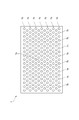
- the electron beam passage hole 7a is one of the many small holes described above and has a point-symmetric shape. Here, as shown in FIG. 5, it is located in the center of the intermediate member 7, and is formed in a circular shape having a diameter of 1 mm or more and 2 mm or less. In other words, the intermediate member 7 is arranged so that the electron beam EB passes through the small hole located in the center among the many small holes formed in the intermediate member 7.
- the shape of the electron beam passage hole 7a may be changed as appropriate, such as a triangle, a quadrangle, a polygon, and an ellipse.
- the intermediate member 7 is disposed so that the electron beam EB passes through the center of the electron beam passage hole 7 a of the intermediate member 7.
- the intermediate member 7 is attached to a holding member (not shown) that holds the condenser mirror 41, and the central axis C of the electron beam passage hole 41 a of the condenser mirror 41 is the intermediate member 7.
- the electron beam passage hole 41a of the condensing mirror 41 and the electron passage hole 7a of the intermediate member 7 are positioned coaxially so as to pass through the center of the electron beam passage hole 7a.
- the light passage hole 7b is a large number of small holes as described above.
- the light passage hole 7b has the same circular shape as the electron beam passage hole 7a.
- These light passage holes 7b are regularly provided, and the distance between the centers of the light passage holes 7b adjacent to each other is set such that the diameter of the light passage hole 7b is not less than 0.2 mm and the diameter of the light passage hole 7b is not more than 1.0 mm.
- the hole area ratio is 30% or more, and the center-to-center distance is 2 mm here.
- the shape of the light passage hole 7b may be changed as appropriate, such as a triangle, a quadrangle, a polygon, and an ellipse, or may be a shape different from that of the electron beam passage hole.
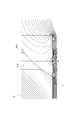
- FIG. 6 and FIG. 7 show the simulation results of the electric field generated when the intermediate member 7 is provided between the sample W and the condenser mirror 41 and a ⁇ 1 V retarding voltage is applied to the sample W. 6 and 7, the intermediate member 7 is indicated by a dotted line in order to make the generation state of the electric field easy to understand.
- the electric field generated by the retarding voltage is made parallel by providing the intermediate member 7 between the sample W and the condenser mirror 41. More specifically, almost no electric field is generated between the collector mirror 41 and the intermediate member 7, and the electric field generated between the intermediate member 7 and the sample W is parallelized. Thereby, the electron beam EB proceeds toward the sample W without bending as much as possible.
- the intermediate member 7 is an electric field collimating unit that parallelizes the electric field generated between the intermediate member 7 and the electric field generated in parallel with the sample W in the present embodiment.
- the electric field does not necessarily have to be completely parallel to the sample, and it is sufficient that the image obtained by the electron microscope in which the sample analyzer 100 is incorporated is substantially parallel to the extent that there is no distortion.
- the horizontal angle is an angle formed by the horizontal direction (lateral direction) of the image and the mesh elements extending in the horizontal direction of the Cu mesh, as shown in FIG.
- the flat intermediate member 7 is provided between the collector mirror 41 and the sample W, the electric field generated between the intermediate member 7 and the sample W can be parallelized. Thereby, it is possible to irradiate the sample W without bending the electron beam EB as much as possible, and to prevent the image obtained by the microscope from being distorted.
- this electric field works as an acceleration voltage for secondary electrons emitted from the sample W. The influence of charging of the sample W can be reduced, and the image obtained by the microscope can be made clearer.
- the electron beam passage hole 41a of the condenser mirror 41 and the electron beam passage hole 7a of the intermediate member 7 are provided coaxially, the electron beam EB passes through the center of the electron beam passage hole 7a of the intermediate member 7.
- the electron beam EB is irradiated to the sample W with almost no bending.
- the electron beam EB is placed at the center of the electron beam passage hole 7a of the intermediate member 7 without positioning the intermediate member 7 each time analysis is performed. Can be passed.
- the intermediate member 7 has a flat plate shape in the embodiment, the intermediate member 7 may have a curved shape symmetric with respect to the central axis.
- a linear metal or the like molded into a rotating body shape can be used.
- the intermediate member 7 has an electron beam passage hole 71 formed at the upper end thereof, and the central axis of the electron beam passage hole 71 and the rotation axis of the intermediate member 7 are connected to the electron passage hole 41 a of the condenser mirror 41. Arranged to coincide with the central axis.
- the electric field generated between the intermediate member 7 and the sample W is distorted by the intermediate member 7, but in the region where the electron beam EB passes, the electric field is emitted from the electron beam irradiation device that is the irradiation unit. Since it is formed perpendicular to the emission direction of the emitted electron beam EB, the emitted electron beam EB can be directed to the sample W with almost no bending.
- the retarding voltage may be applied to the sample W or the sample stage 201 without providing the intermediate member 7 between the sample W and the condenser mirror 41.
- the sensing unit 44 is disposed on the opposite side of the sample mirror W from the collector mirror 41, and an elliptical mirror or the like is used as the collector mirror 41.
- the condenser mirror 41 may be arranged so that its central axis is perpendicular to the sample W.
- the electron beam passage hole and the light passage hole formed in the intermediate member have the same shape.
- the light passage hole is changed to the electron beam passage hole. You may form large compared with.
- the electron beam is irradiated as an energy beam.
- an X-ray, an ion beam, or the like may be irradiated.
- cathode luminescence is measured in the embodiment, other methods such as measuring photoluminescence, Raman light, and the like may be used.
- the light emitted from the measurement sample irradiated with the charged particles is detected to analyze the measurement sample, and the analysis can be performed with higher resolution than before.
Landscapes
- Health & Medical Sciences (AREA)
- Analytical Chemistry (AREA)
- Chemical & Material Sciences (AREA)
- General Health & Medical Sciences (AREA)
- Life Sciences & Earth Sciences (AREA)
- Biochemistry (AREA)
- Physics & Mathematics (AREA)
- General Physics & Mathematics (AREA)
- Immunology (AREA)
- Pathology (AREA)
- Nuclear Medicine, Radiotherapy & Molecular Imaging (AREA)
- Analysing Materials By The Use Of Radiation (AREA)
- Investigating, Analyzing Materials By Fluorescence Or Luminescence (AREA)
Abstract
荷電粒子が照射された測定試料から出る光を検出して前記測定試料を分析する試料分析装置において、従来よりも高い分解能で分析できるようにすべく、荷電粒子を試料Wに照射する照射部3と、照射部3と試料Wとの間に設けられるとともに、試料Wから出る光を集光する集光ミラー41と、試料W又は試料Wが載置される試料台201に荷電粒子を減速させるリターディング電圧を印加するリターディング電圧印加部6とを具備するようにした。
Description
本発明は、例えば電子線やイオンビーム等が照射された測定試料から出る光を検出して、測定試料を分析する試料分析装置及びこの試料分析装置に用いられる集光ミラーユニットに関するものである。
この種の試料分析装置としては、測定試料に電子線を照射することにより生じるカソードルミネッセンス(CL)を検出する、いわゆるカソードルミネッセンス分析装置がある。
ところで、近年、測定試料によっては、例えば電子機器用の各種素子など高集積化や微小化が進んでいるものがあり、これに伴って分析装置に求められる分解能が高まっている。
そこで、特許文献1には、カソードルミネッセンス分析装置の分解能が、測定試料に電子線を照射することにより発生した電子-キャリアの拡散領域に影響することに着目し、測定試料に磁場を印加することでキャリアの拡散を抑制して、分解能の向上を図ったものが記載されている。
しかしながら、これまでの分析装置では、ユーザが求める分解能によってはそのニーズを満足させることができない場合があるし、今後も求められる分解能が高まると予想されることから、分解能をより向上させる必要がある。
そこで本発明は、荷電粒子が照射された測定試料から出る光を検出して前記測定試料を分析する試料分析装置において、従来よりも高い分解能で分析できるようにすることをその主たる所期課題とするものである。
すなわち本発明に係る試料分析装置は、荷電粒子が照射された測定試料から出る光を検出して前記測定試料を分析する試料分析装置において、荷電粒子を前記測定試料に照射する照射部と、前記照射部と前記測定試料との間に設けられるとともに、前記測定試料から出る光を集光する集光ミラーと、前記測定試料又は前記測定試料が載置される試料台に前記荷電粒子を減速させるリターディング電圧を印加するリターディング電圧印加部とを具備することを特徴とするものである。
このようなものであれば、測定試料又は試料台にリターディング電圧を印加するので、照射部から射出された荷電粒子を、高い加速電圧、すなわち高いエネルギーを維持した状態から減速させることができる。その結果、加速電圧を高く維持できるので、エネルギーの色収差などの影響を少なくするとともに、照射部における電子ビームのスポット径を小さくすることができるうえ、仮に試料が壊れやすい場合でも、荷電粒子を照射直前に減速させるので、試料に高いエネルギーの荷電子が照射されて壊れてしまうことを防ぐことができる。これにより、高輝度を維持しつつ、測定試料に照射される荷電粒子の数、すなわち電子ビームのビーム電流を大きくすることができ、測定試料における単位面積当たりに照射される電子数が増加して測定試料から出る光量が多くなり、従来よりも分解能を向上させることが可能となる。
ところで、上述したように測定試料又は試料台にリターディング電圧を印加すると、測定試料や試料台と集光ミラーとの間に電場が生じる。このとき、集光ミラーの電位がゼロであることから、電場は集光ミラーに引き寄せられてミラー面に沿って歪む。そうすると、測定試料に向かう荷電粒子の軌道が曲げられ、得られる画像が歪んでしまうという問題が生じる。
そこで、このような画像の歪みを防ぐためには、荷電粒子が通過する領域において、前記リターディング電圧により生じる電場が、前記照射部から射出される荷電粒子の射出方向に対して垂直に形成されるように構成されていることが好ましい。
なお、ここでいう垂直とは完全に垂直な場合には限られず、得られる画像に歪みがない程度に若干傾いていても構わない。また、ここでいう垂直とは、リターディング電圧により生じる電場が、荷電粒子が通過する領域全体に亘って射出方向に対して垂直である場合のみならず、荷電粒子が通過する領域の一部で傾いている場合も含まれる。
そこで、このような画像の歪みを防ぐためには、荷電粒子が通過する領域において、前記リターディング電圧により生じる電場が、前記照射部から射出される荷電粒子の射出方向に対して垂直に形成されるように構成されていることが好ましい。
なお、ここでいう垂直とは完全に垂直な場合には限られず、得られる画像に歪みがない程度に若干傾いていても構わない。また、ここでいう垂直とは、リターディング電圧により生じる電場が、荷電粒子が通過する領域全体に亘って射出方向に対して垂直である場合のみならず、荷電粒子が通過する領域の一部で傾いている場合も含まれる。
具体的な実施態様としては、試料分析装置が、前記測定試料と前記集光ミラーとの間に設けられ、前記測定試料との間で前記リターディング電圧による電場を生じさせる中間部材をさらに具備するものが挙げられる。
このような構成であれば、電場が集光ミラーに引き寄せられることを防ぐとともに、中間部材の形状や配置によって、中間部材と測定試料との間に荷電粒子がほとんど曲がらないような電場を生じさせることができる。これにより、荷電粒子をできるだけ曲げることなく測定試料に照射させることができ、上述した画像の歪みを防ぐことができる。
このような構成であれば、電場が集光ミラーに引き寄せられることを防ぐとともに、中間部材の形状や配置によって、中間部材と測定試料との間に荷電粒子がほとんど曲がらないような電場を生じさせることができる。これにより、荷電粒子をできるだけ曲げることなく測定試料に照射させることができ、上述した画像の歪みを防ぐことができる。
荷電粒子をほとんど曲げることなく測定試料に照射するためには、前記中間部材が、前記測定試料との間で生じる電場を平行化することが好ましい。
このような中間部材の具体的な実施態様としては、前記測定試料と前記集光ミラーとの間で前記測定試料に対向して設けられた平板状をなすものであり、荷電粒子が中心を通過する荷電粒子通過孔が形成されているものが挙げられる。
このようなものであれば、中間部材が平板状をなし、測定試料に対面して設けられているので、中間部材と測定試料との間に生じる電場を平行化することができる。
そのうえ、荷電粒子が中間部材に形成された荷電粒子孔の中心を通過するので、荷電粒子孔から集光ミラー側に電場が洩れ出たとしても、荷電粒子はこの洩れ出た電場の中心軸に沿ってほとんど曲がることなく測定試料に照射される。
このようなものであれば、中間部材が平板状をなし、測定試料に対面して設けられているので、中間部材と測定試料との間に生じる電場を平行化することができる。
そのうえ、荷電粒子が中間部材に形成された荷電粒子孔の中心を通過するので、荷電粒子孔から集光ミラー側に電場が洩れ出たとしても、荷電粒子はこの洩れ出た電場の中心軸に沿ってほとんど曲がることなく測定試料に照射される。
測定試料から出る光をより多く検出できるようにするためには、前記中間部材が、前記測定試料から出る光を通過させる複数の光通過孔が形成されたものであることが好ましい。
このように複数の光通過孔が形成されていれば、測定試料から出る光の多くが集光ミラーに到達するので、この光をより多く検出することができる。
このように複数の光通過孔が形成されていれば、測定試料から出る光の多くが集光ミラーに到達するので、この光をより多く検出することができる。
本発明に係る電子顕微鏡は、上述した試料分析装置を備えたことを特徴とするものである。
このような電子顕微鏡であれば、上述した試料分析装置と同様の作用効果を得ることができる。
このような電子顕微鏡であれば、上述した試料分析装置と同様の作用効果を得ることができる。
また、本発明に係る試料分析装置用集光ミラーユニットは、測定試料に荷電粒子を照射する照射部と、前記測定試料又は前記測定試料が載置される試料台に前記荷電粒子を減速させるリターディング電圧を印加するリターディング電圧印加部とを具備し、荷電粒子が照射された測定試料から出る光を検出して前記測定試料を分析する試料分析装置に用いられるものであって、前記照射部と前記測定試料との間に設けられるとともに、前記測定試料から出る光を集光することを特徴とするものである。
このような集光ミラーユニットを用いることで、上述した試料分析装置と同様の作用効果を得ることができる。
このような集光ミラーユニットを用いることで、上述した試料分析装置と同様の作用効果を得ることができる。
さらに、上述した画像の歪みを抑えるためには、試料分析装置用集光ミラーユニットが、前記測定試料と前記集光ミラーとの間に設けられ、前記測定試料との間で前記リターディング電圧による電場を生じさせる中間部材を備えることが好ましい。
このように構成した本発明によれば、荷電粒子が照射された測定試料から出る光を検出して前記測定試料を分析する試料分析装置において、従来よりも高分解能な分析が可能となる。
100 ・・・試料分析装置
2 ・・・真空チャンバ
3 ・・・電子線照射装置(照射部)
W ・・・試料
41 ・・・集光ミラー
6 ・・・リターディング電圧印加部
7 ・・・中間部材
2 ・・・真空チャンバ
3 ・・・電子線照射装置(照射部)
W ・・・試料
41 ・・・集光ミラー
6 ・・・リターディング電圧印加部
7 ・・・中間部材
以下に本発明に係る試料分析装置の一実施形態について図面を参照して説明する。
<装置構成>
本実施形態に係る試料分析装置100は、電子顕微鏡に組み込まれたものであり、荷電粒子線である電子線(エネルギー線)EBを半導体ウエハ等の測定試料W(以下、単に試料Wという。)に照射することにより試料Wから生じるカソードルミネッセンスCLを用いて、試料Wの微小領域における物性評価や半導体素子の解析を行う、いわゆるカソードルミネッセンス分析装置である。
本実施形態に係る試料分析装置100は、電子顕微鏡に組み込まれたものであり、荷電粒子線である電子線(エネルギー線)EBを半導体ウエハ等の測定試料W(以下、単に試料Wという。)に照射することにより試料Wから生じるカソードルミネッセンスCLを用いて、試料Wの微小領域における物性評価や半導体素子の解析を行う、いわゆるカソードルミネッセンス分析装置である。
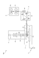
具体的にこのものは、図1に示すように、試料Wを収容する真空チャンバ2と、その真空チャンバ2内に収容された試料Wに電子線EBを照射する照射部たる電子線照射装置3と、電子線EBの照射によって試料Wから発生するカソードルミネッセンスCLを分光し、検出する光検出部たる検出装置4と、その検出装置4からの出力信号を受信し、前記試料Wを評価等(例えば応力測定)するために所定の演算処理を行う情報処理装置5とを備えている。
以下、各部2~5について図1を参照して説明する。
真空チャンバ2は、電子線EBが照射される試料Wを収容する容器と、当該容器内を真空にする真空ポンプと、試料Wが載置される試料台201とを備えている。
電子線照射装置3は、例えば熱電界放出型の電子銃31と、電子銃31から射出された電子線EBを試料Wの所定部位に収束させるレンズ機構及び電子線EBを走査させるための走査機構等からなる電子線制御機構32と、電子銃31及び電子線制御機構32を内部に有する鏡筒33とを備えている。この鏡筒33の下端部は、前記真空チャンバ2の上壁に連続して設けられている。
なお、前記走査機構としては、例えば電子線EBを走査方向に沿って偏向する走査コイルを利用したものが挙げられる。
なお、前記走査機構としては、例えば電子線EBを走査方向に沿って偏向する走査コイルを利用したものが挙げられる。
検出装置4は、集光ミラー41、光ファイバ42、分光部43及びセンシング部44を備えている。
集光ミラー41は、鏡筒33及び試料Wの間(具体的には鏡筒33の下部に設けられるとともに前記レンズ機構を構成する対物レンズと試料Wとの間)に設けられ、試料Wから発生するカソードルミネッセンスCLを集光して光ファイバ42に導くものである。この集光ミラー41は、鏡筒33で収束された電子線EBを通過させ、その電子線EBを試料Wに照射するための電子線通過孔41aと、その電子線通過孔41aの軸線上に焦点が設定されたミラー面41bとを有する。なお、ミラー面41bは、放物面鏡又は楕円面鏡などが考えられるが本実施形態では楕円面鏡を用いている。
光ファイバ42は、集光ミラー41により集光されたカソードルミネッセンスCLを分光部43に転送するものである。この光ファイバ42の受光面である先端面は、集光ミラー41の焦点に配置されるとともに、後端部分が分光部43に接続される。
分光部43は、前記集光ミラー41で集光されたカソードルミネッセンスCLを単色光に分離するもので、例えばモノクロメータを利用して構成している。
センシング部44は、光検出部であり、前記分光部43で波長毎に複数に分光された各単色光の強度をそれぞれ測定し、各単色光の強度に応じた値の電流値(又は電圧値)を有する出力信号を出力する。
情報処理装置5は、構造としては、CPU、メモリ、入出力インターフェイス、AD変換器、入力手段等からなる汎用又は専用のコンピュータである。そして、前記メモリの所定領域に格納してあるプログラムに基づいてCPUやその周辺機器が作動することにより、この情報処理装置5は、前記検出装置4からの出力信号を受信する受信部51と、走査した各測定ポイントでの応力等を算出する演算部52としての機能を発揮する。
そして、本実施形態の試料分析装置100は、図1に示すように、試料Wが載置される試料台201に電子線EBを減速させるリターディング電圧を印加するリターディング電圧印加部6をさらに具備する。
本実施形態では、試料Wと試料台201とは電気的に接続されており、試料台201を介して試料Wにリターディング電圧を印加するようにしているが、試料Wと試料台201とが電気的に接続されていない場合など、試料Wに直接リターディング電圧を印加しても良い。
本実施形態では、試料Wと試料台201とは電気的に接続されており、試料台201を介して試料Wにリターディング電圧を印加するようにしているが、試料Wと試料台201とが電気的に接続されていない場合など、試料Wに直接リターディング電圧を印加しても良い。
リターディング電圧印加部6は、試料台201を介して試料Wに0未満のリターディング電圧を印加するリターディング電源を有するものであり、ここではリターディング電圧を可変にしてある。
このリターディング電圧は、例えば前記情報処理装置5又はこれとは別の処理装置に備えさせたリターディング電圧制御部によって、電子線EBのビーム電流又は電子線照射装置3の加速電圧に基づき制御される。
このリターディング電圧は、例えば前記情報処理装置5又はこれとは別の処理装置に備えさせたリターディング電圧制御部によって、電子線EBのビーム電流又は電子線照射装置3の加速電圧に基づき制御される。
かかる構成により、電子線EBのエネルギー、すなわちビーム電流の大きさは、電子線照射装置3における加速電圧とリターディング電圧との差に応じて決まり、リターディング電圧を変えることにより、試料Wに照射される電子線EBのビーム電流を変えることができる。
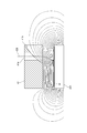
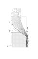
ところで、上述したようにリターディング電圧を印加すると、試料Wと集光ミラー41との間に電場が生じる。このとき、集光ミラー41の電位がゼロであることから、上述した構成のままでは、図2及び図3に示すように、電場は集光ミラー41に引き寄せられてミラー面41bに沿って歪み、試料Wに向かう電子線EBの軌道が曲げられて電子顕微鏡で得られる画像が歪んでしまう。
そこで、本実施形態に係る試料分析装置100は、図4に示すように、試料Wと集光ミラー41との間に設けられ、前記集光ミラー41との間で電場を生じさせることなく、試料Wとの間でリターディング電圧による電場を生じさせる中間部材7をさらに具備している。なお、集光ミラー4と中間部材7との間で電場が生じないようにすべく、中間部材7の電位は集光ミラー4と等電位であり、ここではその電位はゼロである。
本実施形態の中間部材7は、図4に示すように、試料Wと集光ミラー41との間でミラー面41bを覆うように設けられており、ここでは試料Wに対向して試料Wと平行に設けられた平板状をなすものである。なお、中間部材7と試料Wとを必ずしも平行にする必要はなく、例えば試料台201を傾けても構わない。
試料Wと集光ミラー41との離間距離は、集光ミラー41の焦点が試料Wの表面に位置するように設定されており、ここでは3mm程度(もちろん、離間距離はこの値に限らず適宜変更して構わない)である。このことから、中間部材7と試料Wとが近いと、中間部材7と試料Wとの間で放電が生じる恐れがある。そこで、中間部材7は、試料Wとの間で放電が起こらない位置に設けられており、ここでは集光ミラー41に密接して配置されている。
中間部材7の形状は、図5に示すように、中心軸に対して対称な形状をなしており、ここでは平面視矩形状であるが、平面視において円形状、楕円形状、多角形状などであっても良いし、非対称な形状であっても良い。
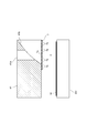
より詳細にこの中間部材7は、図4及び図5に示すように、電子線EBが通過する電子線通過孔7a(請求項でいう荷電粒子通過孔)と、電子線EBが照射された試料Wから出る光を通過させる複数の光通過孔7bとが形成されたものであり、具体的には多数の小孔を有する金属メッシュやパンチングメタルなどである。
電子線通過孔7aは、上述した多数の小孔の1つであり、点対称な形状をなす。ここでは図5に示すように、中間部材7の中央に位置しており、直径は1mm以上2mm以下の円形状に形成されている。言い換えれば、中間部材7に形成された多数の小孔のうち、中央に位置する小孔を電子線EBが通過するように中間部材7を配置している。
なお、電子線通過孔7aの形状は、三角形、四角形、多角形、楕円など、適宜変更して構わない。
なお、電子線通過孔7aの形状は、三角形、四角形、多角形、楕円など、適宜変更して構わない。
さらに、本実施形態では、図4に示すように、中間部材7の電子線通過孔7aの中心を電子線EBが通過するように、中間部材7を配置している。具体的には、中間部材7は、集光ミラー41を保持する図示しない保持部材に前記中間部材7を取り付けられており、集光ミラー41の電子線通過孔41aの中心軸Cが中間部材7の電子線通過孔7aの中心を通るように、つまり集光ミラー41の電子線通過孔41aと中間部材7の電子通過孔7aとが同軸上に位置するようにしてある。
光通過孔7bは、上述した多数の小孔であり、ここでは図5に示すように、前記電子線通過孔7aと同じ円形状をなす。これらの光通過孔7bは、規則的に設けられており、互いに隣り合う光通過孔7bの中心間距離を光通過孔7bの直径+0.2mm以上、光通過孔7bの直径+1.0mm以下で、開孔率が30%以上となるようにしてあり、ここでは中心間距離は2mmである。このような構成であれば、光通過孔7bからの電場の洩れを抑制しつつ、電子線EBが照射された試料Wを出て集光ミラー41に到達する光の光量を十分に確保することができる。
なお、光通過孔7bの形状は、三角形、四角形、多角形、楕円など、適宜変更して構わないし、電子線通過孔と異なる形状であっても構わない。
なお、光通過孔7bの形状は、三角形、四角形、多角形、楕円など、適宜変更して構わないし、電子線通過孔と異なる形状であっても構わない。
ここで、試料Wと集光ミラー41との間に中間部材7を設けて、試料Wに-1Vのリターディング電圧を印加した場合に生じる電場をシミュレーションした結果を図6及び図7に示す。
なお、図6及び図7において、電場の発生状態を分かりやすくすべく、中間部材7は点線で記載してある。
なお、図6及び図7において、電場の発生状態を分かりやすくすべく、中間部材7は点線で記載してある。
このシミュレーション結果から明らかなように、試料Wと集光ミラー41との間に中間部材7を設けることにより、リターディング電圧により生じる電場が平行化されていることが分かる。より詳細には、集光ミラー41と中間部材7との間では電場がほとんど生じず、中間部材7と試料Wとの間で生じる電場が平行化されている。これにより、電子線EBが試料Wに向かって可及的に曲がることなく進むようになる。
このように、中間部材7は、試料Wとの間で生じる電場を平行化する電場平行化手段であり、本実施形態では、前記電場を試料Wに対して平行にしている。
なお、電場は必ずしも試料と完全に平行である必要はなく、試料分析装置100が組み込まれた電子顕微鏡により得られる画像が、実質的に歪みがない程度に平行であれば良い。
なお、電場は必ずしも試料と完全に平行である必要はなく、試料分析装置100が組み込まれた電子顕微鏡により得られる画像が、実質的に歪みがない程度に平行であれば良い。
続いて、試料Wや試料台201にリターディング電圧を印加した状態で電子顕微鏡により得られる画像(SEM像)について、集光ミラー41の有無による違いを確認するために行った実験について述べる。
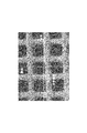
この実験では、試料としてCuメッシュを使用し、リターディング電圧Ebを0kV、0.5kV、1.0kV、1.3kVとしたときに、中間部材7及び集光ミラー41の両方を設けていない場合、中間部材7を設けることなく集光ミラー41を設けた場合、中間部材7及び集光ミラー41の両方を設けた場合それぞれにおいて前記Cuメッシュを観察した。その観察結果を図8に示す。
上段のa、d、g、jから分かるように、集光ミラー41を設けていない場合、リターディング電圧の大きさに関わらず画像の歪みは生じていない。なお、リターディング電圧を大きくすると、得られる画像は低倍率側に移り変わる。
一方、中段のb、e、h、kから分かるように、中間部材7を設けることなく集光ミラー41を設けた場合、リターディング電圧を大きくするほど、画像の歪みが顕著に生じている。これは、リターディング電圧を印加したことにより生じる電場が集光ミラー41に引き寄せられてミラー面41bに沿って歪み、試料Wに向かう電子線EBの軌道が曲げられるからであり、図2及び図3に示すシミュレーション結果と対応した結果であることが分かる。
そして、下段のc、f、i、lから分かるように、集光ミラー41とともに中間部材7を設けた場合、リターディング電圧が大きくなっても画像の歪みが抑制されている。これは、中間部材によって電場が平行化されている証左であり、図6及び図7に示すシミュレーション結果と対応した結果であることが分かる。
そして、下段のc、f、i、lから分かるように、集光ミラー41とともに中間部材7を設けた場合、リターディング電圧が大きくなっても画像の歪みが抑制されている。これは、中間部材によって電場が平行化されている証左であり、図6及び図7に示すシミュレーション結果と対応した結果であることが分かる。
次に、画像の歪みを定量的に評価した結果を以下の表1に示す。

この定量評価から分かるように、集光ミラー41を設けていない場合、リターディング電圧の大きくしても、水平角度はほぼ一定であり、画像の歪みが生じていないことが示されている。
一方、中間部材7を設けることなく集光ミラー41を設けた場合、リターディング電圧を大きくするほど、水平角度が徐々に大きくなっており、画像の歪みが徐々に増していることが示されている。
これに対して、集光ミラー41とともに中間部材7を設けた場合、リターディング電圧の大きくしても、水平角度の変化は小さく、中間部材7によって画像の歪みが抑制されていることが示されている。
一方、中間部材7を設けることなく集光ミラー41を設けた場合、リターディング電圧を大きくするほど、水平角度が徐々に大きくなっており、画像の歪みが徐々に増していることが示されている。
これに対して、集光ミラー41とともに中間部材7を設けた場合、リターディング電圧の大きくしても、水平角度の変化は小さく、中間部材7によって画像の歪みが抑制されていることが示されている。
<本実施形態の効果>
このように構成した本実施形態に係る試料分析装置100によれば、試料台201を介して試料Wにリターディング電圧を印加しているので、電子線照射装置3における電子線EBの加速電圧すなわちビームエネルギーを大きく維持した状態から照射直前で減速させることができる。その結果、色収差などの影響を少なくするとともに、電子線照射装置3における電子線EBのスポット径を小さくすることができるうえ、仮に試料が壊れやすい場合でも、荷電粒子を照射直前に減速させるので、試料に高いエネルギーの荷電子が照射されて壊れてしまうことを防ぐことができ。これにより、輝度を維持しつつ、試料Wに照射される電子の数、つまり電子線EBのビーム電流を大きくすることが可能となり、試料Wにおける単位面積当たりに照射される電子数が増加して試料Wから出るカソードルミネッセンスの光量が多くなり、従来よりも分解能を向上させることが可能となる。
このように構成した本実施形態に係る試料分析装置100によれば、試料台201を介して試料Wにリターディング電圧を印加しているので、電子線照射装置3における電子線EBの加速電圧すなわちビームエネルギーを大きく維持した状態から照射直前で減速させることができる。その結果、色収差などの影響を少なくするとともに、電子線照射装置3における電子線EBのスポット径を小さくすることができるうえ、仮に試料が壊れやすい場合でも、荷電粒子を照射直前に減速させるので、試料に高いエネルギーの荷電子が照射されて壊れてしまうことを防ぐことができ。これにより、輝度を維持しつつ、試料Wに照射される電子の数、つまり電子線EBのビーム電流を大きくすることが可能となり、試料Wにおける単位面積当たりに照射される電子数が増加して試料Wから出るカソードルミネッセンスの光量が多くなり、従来よりも分解能を向上させることが可能となる。
また、集光ミラー41と試料Wとの間に平板状の中間部材7を設けているので、中間部材7と試料Wとの間に生じる電場を平行化することができる。これにより、電子線EBを可及的に曲げることなく試料Wに照射することができ、顕微鏡により得られる画像が歪んでしまうことを防ぐことができる。そのうえ、上述したように、試料Wにリターディング電圧を印加することで電子線EBを減速させる電場を生させているので、この電場が試料Wから放出される二次電子に対する加速電圧として働き、試料Wの帯電の影響を少なくすることができ、顕微鏡により得られる画像をより鮮明にすることができる。
さらに、集光ミラー41の電子線通過孔41aと中間部材7の電子線通過孔7aとを同軸上に設けているので電子線EBが中間部材7の電子線通過孔7aの中心を通るようになり、電子線通過孔7aから集光ミラー41側に電場が洩れ出たとしても、電子線EBはほとんど曲がらずに試料Wに照射される。
そのうえ、集光ミラー41を保持する保持部材に中間部材7を取り付けているので、分析のたびに中間部材7を位置決めすることなく、中間部材7の電子線通過孔7aの中心に電子線EBを通過させることができる。
<その他の変形実施形態>
なお、本発明は前記実施形態に限られるものではない。
なお、本発明は前記実施形態に限られるものではない。
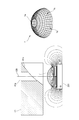
例えば、中間部材7は、前記実施形態では平板状をなすものであったが、中心軸に対して対称な湾曲した形状のものであっても良い。具体的には、図10に示すように、例えば線状の金属などを回転体形状に成型したものなどが挙げられる。この中間部材7は、その上端部に電子線通過孔71が形成されており、この電子線通過孔71の中心軸及び中間部材7の回転軸とが、集光ミラー41の電子通過孔41aの中心軸と一致するように配置されている。
このような中間部材7であれば、中間部材7と試料Wとの間に生じる電場は中間部材7によって歪むものの、電子線EBが通過する領域においては、電場が照射部たる電子線照射装置から射出された電子線EBの射出方向に対して垂直に形成されるので、射出された電子線EBをほとんど曲げることなく試料Wに向かわせることができる。
このような中間部材7であれば、中間部材7と試料Wとの間に生じる電場は中間部材7によって歪むものの、電子線EBが通過する領域においては、電場が照射部たる電子線照射装置から射出された電子線EBの射出方向に対して垂直に形成されるので、射出された電子線EBをほとんど曲げることなく試料Wに向かわせることができる。
また、試料Wと集光ミラー41との間に中間部材7を設けることなく、試料W又は試料台201にリターディング電圧を印加するようにしても良い。
この場合、画像の歪みを抑制するためには、図11に示すように、試料Wに対して集光ミラー41と反対側にセンシング部44を配置するとともに、集光ミラー41として楕円鏡などを用いて、この集光ミラー41をその中心軸が試料Wに対して垂直になるように配置すれば良い。
このような構成であれば、試料Wと集光ミラー41との間で生じる電場は、集光ミラー41によって歪むものの、上述した図10と同様に、電子線EBが通過する領域においては、電場が照射部たる電子線照射装置から射出された電子線EBの射出方向に対して垂直に形成されるので、射出された電子線EBをほとんど曲げることなく試料Wに向かわせることができる。
この場合、画像の歪みを抑制するためには、図11に示すように、試料Wに対して集光ミラー41と反対側にセンシング部44を配置するとともに、集光ミラー41として楕円鏡などを用いて、この集光ミラー41をその中心軸が試料Wに対して垂直になるように配置すれば良い。
このような構成であれば、試料Wと集光ミラー41との間で生じる電場は、集光ミラー41によって歪むものの、上述した図10と同様に、電子線EBが通過する領域においては、電場が照射部たる電子線照射装置から射出された電子線EBの射出方向に対して垂直に形成されるので、射出された電子線EBをほとんど曲げることなく試料Wに向かわせることができる。
さらに、前記実施形態では、中間部材に形成された電子線通過孔と光通過孔とが互いに同じ形状であったが、試料から出る光をより多く検出すべく、光通過孔を電子線通過孔に比べて大きく形成しても良い。
その上、前記実施形態ではエネルギ線として電子線を照射するものをであったが、その他、例えばX線、イオンビーム等を照射するものであっても良い。
加えて、前記実施形態ではカソードルミネッセンスを測定するものであったが、その他、例えばフォトルミネッセンス、ラマン光等を測定するものであっても良い。
その他、本発明は前記実施形態に限られず、その趣旨を逸脱しない範囲で種々の変形が可能であるのは言うまでもない。
本発明に係る試料分析装置であれば、荷電粒子が照射された測定試料から出る光を検出して前記測定試料を分析するものにおいて、従来よりも高い分解能で分析することができる。
Claims (9)
- 荷電粒子が照射された測定試料から出る光を検出して前記測定試料を分析する試料分析装置において、
荷電粒子を前記測定試料に照射する照射部と、
前記照射部と前記測定試料との間に設けられるとともに、前記測定試料から出る光を集光する集光ミラーと、
前記測定試料又は前記測定試料が載置される試料台に前記荷電粒子を減速させるリターディング電圧を印加するリターディング電圧印加部とを具備することを特徴とする試料分析装置。 - 荷電粒子が通過する領域において、前記リターディング電圧により生じる電場が、前記照射部から射出される荷電粒子の射出方向に対して垂直に形成されるように構成されていることを特徴とする請求項1記載の試料分析装置。
- 前記測定試料と前記集光ミラーとの間に設けられ、前記測定試料との間で前記リターディング電圧による電場を生じさせる中間部材をさらに具備することを特徴とする請求項1記載の試料分析装置。
- 前記中間部材が、前記測定試料との間で生じる電場を平行化することを特徴とする請求項3記載の試料分析装置。
- 前記中間部材が、前記測定試料と前記集光ミラーとの間で前記測定試料に対向して設けられた平板状をなすものであり、荷電粒子が中心を通過する荷電粒子通過孔が形成されていることを特徴とする請求項4記載の試料分析装置。
- 前記中間部材が、前記測定試料から出る光を通過させる複数の光通過孔が形成されたものであることを特徴とする請求項3記載の試料分析装置。
- 請求項1記載の試料分析装置を備えた電子顕微鏡。
- 測定試料に荷電粒子を照射する照射部と、前記測定試料又は前記測定試料が載置される試料台に前記荷電粒子を減速させるリターディング電圧を印加するリターディング電圧印加部とを具備し、荷電粒子が照射された測定試料から出る光を検出して前記測定試料を分析する試料分析装置に用いられる集光ミラーユニットであって、
前記照射部と前記測定試料との間に設けられるとともに、前記測定試料から出る光を集光することを特徴とする試料分析装置用集光ミラーユニット。 - 前記測定試料と前記集光ミラーとの間に設けられ、前記測定試料との間で前記リターディング電圧による電場を生じさせる中間部材を備えることを特徴とする請求項8記載の試料分析装置用集光ミラーユニット。
Priority Applications (1)
| Application Number | Priority Date | Filing Date | Title |
|---|---|---|---|
| JP2017563837A JP6754780B2 (ja) | 2016-01-28 | 2017-01-27 | 試料分析装置及び試料分析装置用集光ミラーユニット |
Applications Claiming Priority (2)
| Application Number | Priority Date | Filing Date | Title |
|---|---|---|---|
| JP2016-014919 | 2016-01-28 | ||
| JP2016014919 | 2016-01-28 |
Publications (1)
| Publication Number | Publication Date |
|---|---|
| WO2017131132A1 true WO2017131132A1 (ja) | 2017-08-03 |
Family
ID=59398211
Family Applications (1)
| Application Number | Title | Priority Date | Filing Date |
|---|---|---|---|
| PCT/JP2017/002863 Ceased WO2017131132A1 (ja) | 2016-01-28 | 2017-01-27 | 試料分析装置及び試料分析装置用集光ミラーユニット |
Country Status (2)
| Country | Link |
|---|---|
| JP (1) | JP6754780B2 (ja) |
| WO (1) | WO2017131132A1 (ja) |
Cited By (1)
| Publication number | Priority date | Publication date | Assignee | Title |
|---|---|---|---|---|
| JP2020008516A (ja) * | 2018-07-12 | 2020-01-16 | 株式会社堀場製作所 | 試料分析装置、電子顕微鏡、及び集光ミラーユニット |
Citations (4)
| Publication number | Priority date | Publication date | Assignee | Title |
|---|---|---|---|---|
| JPH05347137A (ja) * | 1992-06-15 | 1993-12-27 | Jeol Ltd | 電子顕微鏡 |
| JP2003106829A (ja) * | 2001-09-28 | 2003-04-09 | Hitachi Ltd | パターン検査方法及びその装置 |
| JP2011133446A (ja) * | 2009-12-25 | 2011-07-07 | Mitsubishi Electric Corp | 半導体基板の欠陥検査装置および欠陥検査方法 |
| JP2012028019A (ja) * | 2010-07-20 | 2012-02-09 | Horiba Ltd | 集光器装置 |
Family Cites Families (5)
| Publication number | Priority date | Publication date | Assignee | Title |
|---|---|---|---|---|
| JP2003014671A (ja) * | 2001-06-29 | 2003-01-15 | Canon Inc | 固体表面観察装置と固体表面観察方法 |
| JP2004047284A (ja) * | 2002-07-12 | 2004-02-12 | Toray Res Center:Kk | カソードルミネッセンス複合装置および該複合装置を用いた測定方法 |
| JP4894990B2 (ja) * | 2005-03-09 | 2012-03-14 | 奥野製薬工業株式会社 | 酸性電気銅めっき液 |
| JP4696197B2 (ja) * | 2005-09-06 | 2011-06-08 | 独立行政法人産業技術総合研究所 | カソードルミネッセンス検出装置 |
| JP2011060555A (ja) * | 2009-09-09 | 2011-03-24 | Tokuyama Corp | 真空紫外線の検出方法および走査電子顕微鏡 |
-
2017
- 2017-01-27 WO PCT/JP2017/002863 patent/WO2017131132A1/ja not_active Ceased
- 2017-01-27 JP JP2017563837A patent/JP6754780B2/ja active Active
Patent Citations (4)
| Publication number | Priority date | Publication date | Assignee | Title |
|---|---|---|---|---|
| JPH05347137A (ja) * | 1992-06-15 | 1993-12-27 | Jeol Ltd | 電子顕微鏡 |
| JP2003106829A (ja) * | 2001-09-28 | 2003-04-09 | Hitachi Ltd | パターン検査方法及びその装置 |
| JP2011133446A (ja) * | 2009-12-25 | 2011-07-07 | Mitsubishi Electric Corp | 半導体基板の欠陥検査装置および欠陥検査方法 |
| JP2012028019A (ja) * | 2010-07-20 | 2012-02-09 | Horiba Ltd | 集光器装置 |
Cited By (2)
| Publication number | Priority date | Publication date | Assignee | Title |
|---|---|---|---|---|
| JP2020008516A (ja) * | 2018-07-12 | 2020-01-16 | 株式会社堀場製作所 | 試料分析装置、電子顕微鏡、及び集光ミラーユニット |
| JP7072457B2 (ja) | 2018-07-12 | 2022-05-20 | 株式会社堀場製作所 | 試料分析装置、電子顕微鏡、及び集光ミラーユニット |
Also Published As
| Publication number | Publication date |
|---|---|
| JPWO2017131132A1 (ja) | 2018-11-22 |
| JP6754780B2 (ja) | 2020-09-16 |
Similar Documents
| Publication | Publication Date | Title |
|---|---|---|
| CN100521062C (zh) | 粒子-光学装置与检测装置 | |
| JP5948083B2 (ja) | 走査電子顕微鏡 | |
| US8183526B1 (en) | Mirror monochromator for charged particle beam apparatus | |
| JP2005539359A (ja) | 粒子−光デバイスおよび検出手段 | |
| JPWO2017183086A1 (ja) | 質量分析装置 | |
| US20200251305A1 (en) | Charged particle beam apparatus | |
| US20160217969A1 (en) | Charged Particle Beam Inclination Correction Method and Charged Particle Beam Device | |
| JP2014053304A (ja) | 荷電粒子レンズ系における収差を調査及び補正する方法 | |
| WO2017010529A1 (ja) | 静電レンズ、並びに、該レンズとコリメータを用いた平行ビーム発生装置及び平行ビーム収束装置 | |
| JP2026040580A (ja) | 走査型電子顕微鏡および走査型電子顕微鏡の2次電子検出方法 | |
| JP6412952B2 (ja) | 走査電子顕微鏡およびその電子軌道調整方法 | |
| JP6266467B2 (ja) | 電子顕微鏡、およびモノクロメーターの調整方法 | |
| JP2004513477A (ja) | 静電対物に調整可能な最終電極を設けたsem | |
| JP6754780B2 (ja) | 試料分析装置及び試料分析装置用集光ミラーユニット | |
| CN109904053A (zh) | 具有改进eels/eftem模块的透射带电粒子显微镜 | |
| JP2018190731A (ja) | 粒子ビームを生成するための粒子源及び粒子光学装置 | |
| US11348757B2 (en) | Charged particle beam device | |
| JP4920539B2 (ja) | カソードルミネッセンス測定装置及び電子顕微鏡 | |
| JP7072457B2 (ja) | 試料分析装置、電子顕微鏡、及び集光ミラーユニット | |
| JP2015043348A (ja) | 荷電粒子線装置 | |
| JP3814968B2 (ja) | 検査装置 | |
| JP2022071081A (ja) | 電子ビーム・イオン発生装置および電子ビーム・イオン発生方法 | |
| JP2022071076A (ja) | 走査型電子顕微鏡および走査型電子顕微鏡の2次電子検出方法 | |
| JP6518442B2 (ja) | 電子検出装置および走査電子顕微鏡 | |
| JP2000208080A (ja) | 電子銃及び該電子銃を用いた装置 |
Legal Events
| Date | Code | Title | Description |
|---|---|---|---|
| 121 | Ep: the epo has been informed by wipo that ep was designated in this application |
Ref document number: 17744362 Country of ref document: EP Kind code of ref document: A1 |
|
| ENP | Entry into the national phase |
Ref document number: 2017563837 Country of ref document: JP Kind code of ref document: A |
|
| NENP | Non-entry into the national phase |
Ref country code: DE |
|
| 122 | Ep: pct application non-entry in european phase |
Ref document number: 17744362 Country of ref document: EP Kind code of ref document: A1 |