WO2017130634A1 - 露光装置および露光方法 - Google Patents
露光装置および露光方法 Download PDFInfo
- Publication number
- WO2017130634A1 WO2017130634A1 PCT/JP2016/089182 JP2016089182W WO2017130634A1 WO 2017130634 A1 WO2017130634 A1 WO 2017130634A1 JP 2016089182 W JP2016089182 W JP 2016089182W WO 2017130634 A1 WO2017130634 A1 WO 2017130634A1
- Authority
- WO
- WIPO (PCT)
- Prior art keywords
- master
- exposure apparatus
- focus
- laser beam
- shape data
- Prior art date
- Legal status (The legal status is an assumption and is not a legal conclusion. Google has not performed a legal analysis and makes no representation as to the accuracy of the status listed.)
- Ceased
Links
Images






Classifications
-
- G—PHYSICS
- G03—PHOTOGRAPHY; CINEMATOGRAPHY; ANALOGOUS TECHNIQUES USING WAVES OTHER THAN OPTICAL WAVES; ELECTROGRAPHY; HOLOGRAPHY
- G03F—PHOTOMECHANICAL PRODUCTION OF TEXTURED OR PATTERNED SURFACES, e.g. FOR PRINTING, FOR PROCESSING OF SEMICONDUCTOR DEVICES; MATERIALS THEREFOR; ORIGINALS THEREFOR; APPARATUS SPECIALLY ADAPTED THEREFOR
- G03F7/00—Photomechanical, e.g. photolithographic, production of textured or patterned surfaces, e.g. printing surfaces; Materials therefor, e.g. comprising photoresists; Apparatus specially adapted therefor
- G03F7/20—Exposure; Apparatus therefor
- G03F7/2051—Exposure without an original mask, e.g. using a programmed deflection of a point source, by scanning, by drawing with a light beam, using an addressed light or corpuscular source
- G03F7/2053—Exposure without an original mask, e.g. using a programmed deflection of a point source, by scanning, by drawing with a light beam, using an addressed light or corpuscular source using a laser
-
- G—PHYSICS
- G03—PHOTOGRAPHY; CINEMATOGRAPHY; ANALOGOUS TECHNIQUES USING WAVES OTHER THAN OPTICAL WAVES; ELECTROGRAPHY; HOLOGRAPHY
- G03F—PHOTOMECHANICAL PRODUCTION OF TEXTURED OR PATTERNED SURFACES, e.g. FOR PRINTING, FOR PROCESSING OF SEMICONDUCTOR DEVICES; MATERIALS THEREFOR; ORIGINALS THEREFOR; APPARATUS SPECIALLY ADAPTED THEREFOR
- G03F7/00—Photomechanical, e.g. photolithographic, production of textured or patterned surfaces, e.g. printing surfaces; Materials therefor, e.g. comprising photoresists; Apparatus specially adapted therefor
- G03F7/0002—Lithographic processes using patterning methods other than those involving the exposure to radiation, e.g. by stamping
-
- G—PHYSICS
- G03—PHOTOGRAPHY; CINEMATOGRAPHY; ANALOGOUS TECHNIQUES USING WAVES OTHER THAN OPTICAL WAVES; ELECTROGRAPHY; HOLOGRAPHY
- G03F—PHOTOMECHANICAL PRODUCTION OF TEXTURED OR PATTERNED SURFACES, e.g. FOR PRINTING, FOR PROCESSING OF SEMICONDUCTOR DEVICES; MATERIALS THEREFOR; ORIGINALS THEREFOR; APPARATUS SPECIALLY ADAPTED THEREFOR
- G03F7/00—Photomechanical, e.g. photolithographic, production of textured or patterned surfaces, e.g. printing surfaces; Materials therefor, e.g. comprising photoresists; Apparatus specially adapted therefor
- G03F7/70—Microphotolithographic exposure; Apparatus therefor
- G03F7/70008—Production of exposure light, i.e. light sources
- G03F7/70025—Production of exposure light, i.e. light sources by lasers
-
- G—PHYSICS
- G03—PHOTOGRAPHY; CINEMATOGRAPHY; ANALOGOUS TECHNIQUES USING WAVES OTHER THAN OPTICAL WAVES; ELECTROGRAPHY; HOLOGRAPHY
- G03F—PHOTOMECHANICAL PRODUCTION OF TEXTURED OR PATTERNED SURFACES, e.g. FOR PRINTING, FOR PROCESSING OF SEMICONDUCTOR DEVICES; MATERIALS THEREFOR; ORIGINALS THEREFOR; APPARATUS SPECIALLY ADAPTED THEREFOR
- G03F7/00—Photomechanical, e.g. photolithographic, production of textured or patterned surfaces, e.g. printing surfaces; Materials therefor, e.g. comprising photoresists; Apparatus specially adapted therefor
- G03F7/70—Microphotolithographic exposure; Apparatus therefor
- G03F7/70008—Production of exposure light, i.e. light sources
- G03F7/70033—Production of exposure light, i.e. light sources by plasma extreme ultraviolet [EUV] sources
-
- G—PHYSICS
- G03—PHOTOGRAPHY; CINEMATOGRAPHY; ANALOGOUS TECHNIQUES USING WAVES OTHER THAN OPTICAL WAVES; ELECTROGRAPHY; HOLOGRAPHY
- G03F—PHOTOMECHANICAL PRODUCTION OF TEXTURED OR PATTERNED SURFACES, e.g. FOR PRINTING, FOR PROCESSING OF SEMICONDUCTOR DEVICES; MATERIALS THEREFOR; ORIGINALS THEREFOR; APPARATUS SPECIALLY ADAPTED THEREFOR
- G03F7/00—Photomechanical, e.g. photolithographic, production of textured or patterned surfaces, e.g. printing surfaces; Materials therefor, e.g. comprising photoresists; Apparatus specially adapted therefor
- G03F7/70—Microphotolithographic exposure; Apparatus therefor
- G03F7/70058—Mask illumination systems
- G03F7/70141—Illumination system adjustment, e.g. adjustments during exposure or alignment during assembly of illumination system
-
- G—PHYSICS
- G03—PHOTOGRAPHY; CINEMATOGRAPHY; ANALOGOUS TECHNIQUES USING WAVES OTHER THAN OPTICAL WAVES; ELECTROGRAPHY; HOLOGRAPHY
- G03F—PHOTOMECHANICAL PRODUCTION OF TEXTURED OR PATTERNED SURFACES, e.g. FOR PRINTING, FOR PROCESSING OF SEMICONDUCTOR DEVICES; MATERIALS THEREFOR; ORIGINALS THEREFOR; APPARATUS SPECIALLY ADAPTED THEREFOR
- G03F7/00—Photomechanical, e.g. photolithographic, production of textured or patterned surfaces, e.g. printing surfaces; Materials therefor, e.g. comprising photoresists; Apparatus specially adapted therefor
- G03F7/70—Microphotolithographic exposure; Apparatus therefor
- G03F7/70216—Mask projection systems
- G03F7/70275—Multiple projection paths, e.g. array of projection systems, microlens projection systems or tandem projection systems
-
- G—PHYSICS
- G03—PHOTOGRAPHY; CINEMATOGRAPHY; ANALOGOUS TECHNIQUES USING WAVES OTHER THAN OPTICAL WAVES; ELECTROGRAPHY; HOLOGRAPHY
- G03F—PHOTOMECHANICAL PRODUCTION OF TEXTURED OR PATTERNED SURFACES, e.g. FOR PRINTING, FOR PROCESSING OF SEMICONDUCTOR DEVICES; MATERIALS THEREFOR; ORIGINALS THEREFOR; APPARATUS SPECIALLY ADAPTED THEREFOR
- G03F7/00—Photomechanical, e.g. photolithographic, production of textured or patterned surfaces, e.g. printing surfaces; Materials therefor, e.g. comprising photoresists; Apparatus specially adapted therefor
- G03F7/70—Microphotolithographic exposure; Apparatus therefor
- G03F7/70483—Information management; Active and passive control; Testing; Wafer monitoring, e.g. pattern monitoring
- G03F7/70605—Workpiece metrology
- G03F7/70616—Monitoring the printed patterns
- G03F7/70641—Focus
-
- G—PHYSICS
- G03—PHOTOGRAPHY; CINEMATOGRAPHY; ANALOGOUS TECHNIQUES USING WAVES OTHER THAN OPTICAL WAVES; ELECTROGRAPHY; HOLOGRAPHY
- G03F—PHOTOMECHANICAL PRODUCTION OF TEXTURED OR PATTERNED SURFACES, e.g. FOR PRINTING, FOR PROCESSING OF SEMICONDUCTOR DEVICES; MATERIALS THEREFOR; ORIGINALS THEREFOR; APPARATUS SPECIALLY ADAPTED THEREFOR
- G03F7/00—Photomechanical, e.g. photolithographic, production of textured or patterned surfaces, e.g. printing surfaces; Materials therefor, e.g. comprising photoresists; Apparatus specially adapted therefor
- G03F7/70—Microphotolithographic exposure; Apparatus therefor
- G03F7/70483—Information management; Active and passive control; Testing; Wafer monitoring, e.g. pattern monitoring
- G03F7/70605—Workpiece metrology
- G03F7/706835—Metrology information management or control
-
- G—PHYSICS
- G03—PHOTOGRAPHY; CINEMATOGRAPHY; ANALOGOUS TECHNIQUES USING WAVES OTHER THAN OPTICAL WAVES; ELECTROGRAPHY; HOLOGRAPHY
- G03F—PHOTOMECHANICAL PRODUCTION OF TEXTURED OR PATTERNED SURFACES, e.g. FOR PRINTING, FOR PROCESSING OF SEMICONDUCTOR DEVICES; MATERIALS THEREFOR; ORIGINALS THEREFOR; APPARATUS SPECIALLY ADAPTED THEREFOR
- G03F7/00—Photomechanical, e.g. photolithographic, production of textured or patterned surfaces, e.g. printing surfaces; Materials therefor, e.g. comprising photoresists; Apparatus specially adapted therefor
- G03F7/70—Microphotolithographic exposure; Apparatus therefor
- G03F7/70483—Information management; Active and passive control; Testing; Wafer monitoring, e.g. pattern monitoring
- G03F7/70605—Workpiece metrology
- G03F7/706843—Metrology apparatus
- G03F7/706845—Calibration, e.g. tool-to-tool calibration, beam alignment, spot position or focus
-
- G—PHYSICS
- G03—PHOTOGRAPHY; CINEMATOGRAPHY; ANALOGOUS TECHNIQUES USING WAVES OTHER THAN OPTICAL WAVES; ELECTROGRAPHY; HOLOGRAPHY
- G03F—PHOTOMECHANICAL PRODUCTION OF TEXTURED OR PATTERNED SURFACES, e.g. FOR PRINTING, FOR PROCESSING OF SEMICONDUCTOR DEVICES; MATERIALS THEREFOR; ORIGINALS THEREFOR; APPARATUS SPECIALLY ADAPTED THEREFOR
- G03F7/00—Photomechanical, e.g. photolithographic, production of textured or patterned surfaces, e.g. printing surfaces; Materials therefor, e.g. comprising photoresists; Apparatus specially adapted therefor
- G03F7/70—Microphotolithographic exposure; Apparatus therefor
- G03F7/708—Construction of apparatus, e.g. environment aspects, hygiene aspects or materials
- G03F7/7085—Detection arrangement, e.g. detectors of apparatus alignment possibly mounted on wafers, exposure dose, photo-cleaning flux, stray light, thermal load
-
- H—ELECTRICITY
- H01—ELECTRIC ELEMENTS
- H01S—DEVICES USING THE PROCESS OF LIGHT AMPLIFICATION BY STIMULATED EMISSION OF RADIATION [LASER] TO AMPLIFY OR GENERATE LIGHT; DEVICES USING STIMULATED EMISSION OF ELECTROMAGNETIC RADIATION IN WAVE RANGES OTHER THAN OPTICAL
- H01S3/00—Lasers, i.e. devices using stimulated emission of electromagnetic radiation in the infrared, visible or ultraviolet wave range
- H01S3/10—Controlling the intensity, frequency, phase, polarisation or direction of the emitted radiation, e.g. switching, gating, modulating or demodulating
- H01S3/106—Controlling the intensity, frequency, phase, polarisation or direction of the emitted radiation, e.g. switching, gating, modulating or demodulating by controlling devices placed within the cavity
-
- H—ELECTRICITY
- H10—SEMICONDUCTOR DEVICES; ELECTRIC SOLID-STATE DEVICES NOT OTHERWISE PROVIDED FOR
- H10P—GENERIC PROCESSES OR APPARATUS FOR THE MANUFACTURE OR TREATMENT OF DEVICES COVERED BY CLASS H10
- H10P76/00—Manufacture or treatment of masks on semiconductor bodies, e.g. by lithography or photolithography
-
- H—ELECTRICITY
- H01—ELECTRIC ELEMENTS
- H01S—DEVICES USING THE PROCESS OF LIGHT AMPLIFICATION BY STIMULATED EMISSION OF RADIATION [LASER] TO AMPLIFY OR GENERATE LIGHT; DEVICES USING STIMULATED EMISSION OF ELECTROMAGNETIC RADIATION IN WAVE RANGES OTHER THAN OPTICAL
- H01S3/00—Lasers, i.e. devices using stimulated emission of electromagnetic radiation in the infrared, visible or ultraviolet wave range
- H01S3/10—Controlling the intensity, frequency, phase, polarisation or direction of the emitted radiation, e.g. switching, gating, modulating or demodulating
- H01S3/13—Stabilisation of laser output parameters, e.g. frequency or amplitude
- H01S3/1305—Feedback control systems
Definitions
- the present invention relates to an exposure apparatus and an exposure method for exposing and forming a pattern by irradiating a master disk with laser light.
- a fine pattern on a master is transferred to a resin sheet by pressing a flat or cylindrical (columnar) master with a fine pattern on the surface against the resin sheet.
- a flat or cylindrical (columnar) master with a fine pattern on the surface against the resin sheet.
- nanoimprint technology There is nanoimprint technology.
- Patent Document 1 discloses an exposure apparatus for forming a fine pattern on the surface of a master.
- This exposure apparatus includes a spindle that sandwiches and holds a cylindrical master from both end faces, and a light source that emits a laser beam (laser light). Then, while rotating the master having the surface coated with the thermal reaction resist or the photoreactive resist, the master disc is irradiated (exposed) with the laser beam emitted from the light source in accordance with the desired pattern, and the thermal reaction resist or the photoreactive resist. To form a desired pattern on the surface of the master.
- this exposure apparatus receives a laser beam reflected by the master by a four-divided detector whose light-receiving surface is divided into four, and performs focus control of the laser beam according to the light reception result.
- FIG. 5 is a view showing an example of the configuration of an exposure apparatus that performs focus control.
- the exposure apparatus 100 shown in FIG. 5 includes a spindle motor 11, an optical pickup 12, an optical sensor 13, an error calculation unit 14, a subtractor 150, a control calculation unit 16, and an amplification unit 17.
- the spindle motor 11 has a cylindrical (or columnar) master 1 placed thereon and rotates the placed master 1 in the circumferential direction.
- the optical pickup 12 emits a laser beam toward the master 1 placed on the spindle motor 11.
- the optical pickup 12 is slidable in the axial direction of the master 1, and the optical pickup 12 is slid along the axial direction of the master 1 while rotating the master 1 by the spindle motor 11.
- the surface of the master 1 can be irradiated with laser light emitted from the master 12.
- a thermal reaction resist or a photoreaction resist is applied and formed, and by irradiating the laser beam, the part of the thermal reaction resist or the photoreaction resist irradiated with the laser beam is reacted, A pattern can be exposed and formed in an arbitrary region on the surface of the master 1.
- the optical pickup 12 includes a laser light source 121, a collimator lens 122, a polarization beam splitter 123, an objective lens 124, an actuator 125, and a cylindrical lens 126.
- the laser light source 121 outputs laser light.
- the collimator lens 122 collimates the laser beam output from the laser light source 121 and outputs it to the polarization beam splitter 123.
- the polarization beam splitter 123 transmits the laser light output from the collimator lens 122 toward the objective lens 124.
- the polarization beam splitter 123 reflects the reflected light incident on the objective lens 124 to the cylindrical lens 126 after the laser beam emitted from the optical pickup 12 is reflected by the master 1.
- the objective lens 124 condenses the laser beam that has passed through the polarization beam splitter 123 and emits it toward the master 1.
- the actuator 125 displaces (moves back and forth) the objective lens 124 along the direction toward the master 1. By displacing the objective lens 124, the focal position of the emitted laser light changes. Therefore, the optical pickup 12 can adjust the focus of the laser beam.
- the cylindrical lens 126 condenses the light (reflected light from the master 1) reflected by the polarization beam splitter 123 on the light receiving surface of the optical sensor 13.
- the optical sensor 13 is a sensor that receives light from the cylindrical lens 126 (reflected light from the master 1) on a light receiving surface and outputs the light according to the received light.
- the optical sensor 13 is a four-division PD (Photo Diode). is there.
- the optical sensor 13 includes a light receiving surface divided into four regions (regions A, B, C, and D).
- the optical sensor 13 When the laser light emitted to the master 1 is focused on the surface of the master 1, the light received by the light receiving surface of the optical sensor 13 becomes a perfect circle as shown in FIG. ⁇ D is almost equal.
- the light received by the light receiving surface of the optical sensor 13 is As shown to 7B and 7C, it becomes an elliptical and slanting shape.
- the optical sensor 13 outputs the voltages V A to V D corresponding to the lights irradiated to the areas A to D to the error calculator 14.
- the error calculation unit 14 outputs a focus error voltage corresponding to the focus error of the laser beam emitted to the master 1.
- the subtractor 150 calculates a difference between the target value and the output (focus error voltage) of the error calculation unit 14, and outputs the calculated difference to the control calculation unit 16.
- the target value is, for example, a value corresponding to the output voltage of the error calculator 14 when the laser beam emitted to the master 1 is focused on the surface of the master 1.
- the control calculation unit 16 generates a control signal for the actuator 125 for moving the objective lens 124 so that the difference calculated by the subtracter 150 becomes zero, and outputs the control signal to the amplification unit 17.
- the control calculating part 16 produces
- PID control proportional integral control
- the amplification unit 17 amplifies the control signal output from the control calculation unit 16 and outputs the amplified control signal to the actuator 125. Therefore, the actuator 125 is controlled so that the difference calculated by the subtracter 150 becomes zero.
- the exposure apparatus 100 has an autofocus function that adjusts the focal position of the laser beam so as to suppress the focus error.
- the focus error cannot be completely removed, and the loop transfer function (gain) in the entire loop (focus servo loop) from the subtracter 150 to the error calculation unit 14 can be obtained.
- An error of about 1 (left-over error) occurs.
- the relative position relationship between the optical pickup 12 and the surface of the master 1 is affected by the roughness (unevenness) of the master surface, the inclination and eccentricity of the master, and the like. If the variation is large, the remaining error also becomes large. If the residual error becomes large, it becomes impossible to perform exposure exposure of the pattern on the master with high accuracy.
- An object of the present invention is to provide an exposure apparatus and an exposure method capable of solving the above-described problems and performing exposure exposure of a pattern on a master with higher accuracy while suppressing an increase in cost.
- an exposure apparatus is an exposure apparatus that irradiates a laser beam onto a placed master and exposes a pattern, and emits the laser light to focus the laser light.
- a light source device capable of adjusting a relative position relationship between the surface of the master and the light source device according to at least one of the surface roughness of the master, the inclination of the master, and the eccentricity of the master
- a controller that adjusts the focus of the laser light emitted from the light source device using surface shape data.
- the control unit includes an error detection unit that performs output in accordance with a focus error of the laser beam, and the laser beam is combined on the surface of the master.
- An adder for adding a target value corresponding to an output from the error detection unit in a focused state and an offset value based on a correction signal generated based on the total surface shape data, and an addition by the adder It is preferable to include a control calculation unit that adjusts the focus of the laser beam based on a difference between the value and the output of the error detection unit.
- the correction signal is a table or a function corresponding to the position of the surface of the master.
- the control unit includes: An error detection unit that performs output in accordance with a focus error of the laser beam, and a predetermined calculation process based on the total surface shape data for the output of the error detection unit, so that the laser beam is A calculation unit for calculating an offset value for correcting a target value corresponding to an output from the error detection unit in a focused state on the surface, and the target value and the offset value calculated by the calculation unit. It is preferable to include an adder for adding, and a control calculation unit that adjusts the focus of the laser beam based on the difference between the addition value obtained by the adder and the output of the error detection unit.
- the light source device is an optical pickup, and the total surface shape data is measured by the optical pickup.
- the optical pickup includes an optical sensor that outputs a voltage corresponding to a focus error of the laser beam, and the total surface shape data is stored in the optical sensor. It is preferable to measure based on the output.
- the optical pickup includes an objective lens that emits the laser light to the master and an actuator that displaces the objective lens, and the overall surface
- the shape data is preferably measured based on the current flowing through the actuator.
- the total surface shape data is preferably measured by a displacement meter.
- the master is a cylindrical or columnar master.
- the master is preferably a flat master.
- an exposure method includes a light source device that emits laser light and can adjust the focus of the laser light, and irradiates the placed master with the laser light.
- An exposure method by an exposure apparatus for exposing and forming a pattern, wherein the surface of the master and the light source device are relative to each other according to at least one of the surface roughness of the master, the inclination of the master, and the eccentricity of the master It is preferable to adjust the focus of the laser beam emitted from the light source device by using the total surface shape data indicating a proper positional relationship.
- the exposure apparatus and the exposure method of the present invention it is possible to perform pattern exposure on the master with higher accuracy while suppressing an increase in cost.
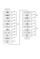
- FIG. 3 is a flowchart showing an example of the operation of the exposure apparatus shown in FIG. It is a figure which shows an example of a structure of the exposure apparatus which concerns on the 2nd Embodiment of this invention.
- 4 is a flowchart showing an example of the operation of the exposure apparatus shown in FIG. It is a figure which shows an example of a structure of the exposure apparatus which performs focus control. It is a figure which shows an example of the light-receiving surface of the optical sensor shown in FIG. It is a figure which shows an example of the light reception state in the light-receiving surface of the optical sensor shown in FIG. It is a figure which shows an example of the light reception state in the light-receiving surface of the optical sensor shown in FIG. It is a figure which shows an example of the light reception state in the light-receiving surface of the optical sensor shown in FIG. It is a figure which shows an example of the light reception state in the light-receiving surface of the optical sensor shown in FIG.
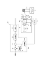
- FIG. 1 is a view showing an example of the configuration of an exposure apparatus 10 according to the first embodiment of the present invention.
- the same components as those of the exposure apparatus 100 shown in FIG. 1 are identical to the same components as those of the exposure apparatus 100 shown in FIG.
- the exposure apparatus 10 shown in FIG. 1 is different from the exposure apparatus 100 shown in FIG. 5 in that an adder 18 is added and a subtracter 150 is changed to a subtracter 15. That is, the exposure apparatus 10 includes a spindle motor 11, an optical pickup 12 (light source device), an optical sensor 13, an error calculation unit 14 (error detection unit), a subtractor 15, a control calculation unit 16, and an amplification unit. 17 and an adder 18.
- the error calculation unit 14, the subtractor 15, the control calculation unit 16, the amplification unit 17, and the adder 18 constitute a control unit 19.
- the optical pickup 12 and the optical sensor 13 are described separately, but the optical sensor 13 may be included in the optical pickup 12.
- the control unit 19 compares the optical pickup 12 and the surface of the master 1 in accordance with at least one of the roughness (unevenness) of the surface of the master 1 placed on the spindle motor 11, the inclination and the eccentricity of the master 1.
- the total surface shape data which is the measurement result of the positional relationship, is acquired.
- the control unit 19 makes the focus error that cannot be removed by the focus servo loop from the subtractor 15 to the error calculation unit 14 become zero at each position on the surface of the master 1 based on the acquired total surface shape data.
- a correction signal for correcting the target value is generated and held in a storage unit (not shown) in FIG.
- the correction signal is represented by, for example, a table or a function.
- a focus offset (offset value) to be added to the target value is input to the adder 18 according to the position on the surface of the master 1 to be exposed.
- the adder 18 adds the target value and the focus offset based on the correction signal, and outputs the added value to the subtracter 15.
- the subtractor 15 calculates the difference between the output value of the adder 18 and the focus error voltage output from the error calculation unit 14, and outputs the calculation result to the control calculation unit 16. Thereafter, similarly to the exposure apparatus 100 shown in FIG. 5, the actuator 125 is controlled so that the difference calculated by the subtracter 15 becomes zero. As described above, in the exposure apparatus 100 shown in FIG. 5, even if control is performed so that the difference between the target value and the focus error voltage becomes zero, the focus servo loop loop transfer function (focus servo transfer function) is reduced. Some degree of focus error remains.
- the exposure apparatus 10 based on the acquired total surface shape data, a focus offset for correcting the target value is added to the target value so that the focus error that cannot be removed by the focus servo loop becomes zero. Therefore, the focus error can be suppressed with higher accuracy, and as a result, the pattern can be exposed and formed on the master 1 with higher accuracy.
- the autofocus function is turned on (the focus servo loop is enabled), the rotation speed of the spindle motor 11 is set to a predetermined value, and the slide speed of the optical pickup 12 is set to a predetermined value. Set.
- a laser beam is emitted from the optical pickup 12 to such an extent that the thermal reaction resist or photoreaction resist applied to the surface of the master 1 does not react (with an irradiation amount and an irradiation time at which the thermal reaction resist or photoreaction resist does not react)
- the whole surface or a part of the master 1 is scanned.
- the focus error voltage output from the error calculator 14 is measured at a predetermined sampling rate.
- the focus error can be suppressed by the feedback control by the focus servo loop, but the focus error cannot be completely removed, and an error of about one part of the focus servo transfer function remains. This error appears as a focus error voltage output from the error calculator 14.
- the focus servo transfer function is known, comprehensive surface shape data that is a relative positional relationship between the surface of the master 1 and the optical pickup 12 is acquired from the focus error voltage output from the error calculator 14. be able to.
- a correction signal (table or function) for adjusting the focus offset so that the focus error voltage becomes zero is calculated.
- the generation of the correction signal is not limited to the method using the focus error voltage described above.
- the correction signal can be generated using a current (VCM current) flowing through the actuator 125.
- VCM current current flowing through the actuator 125.
- a method for generating a correction signal using the VCM current will be described.
- the autofocus function is turned on (the focus servo loop is enabled), the rotation speed of the spindle motor 11 is set to a predetermined value, and the slide speed of the optical pickup 12 is set to a predetermined value. Set.
- the VCM current is measured at a predetermined sampling rate.
- the actuator 125 is driven so as to suppress the focus error by the autofocus function. Therefore, the VCM current indicates the amount of displacement of the objective lens 124, that is, the relative positional relationship between the surface of the master 1 and the optical pickup 12, and the total surface shape data is obtained by measuring the VCM current. can do.
- the correction signal is generated based on the focus error voltage, the error becomes large.
- the amount of displacement of the objective lens 124 is calculated from the VCM current, a leftover error is predicted from the amount of displacement, the focus servo transfer function, and the characteristics of the optical sensor 13, and correction is performed to compensate for the leftover error. Generate a signal. By doing so, a highly accurate correction signal can be generated.
- both the focus error voltage and the VCM current may be measured, and a correction signal may be generated from these measurement results.
- the optical sensor 13 may be included in the optical pickup 12, and the focus error voltage and the VCM current can be detected by the optical pickup 12. Therefore, the focus error voltage and the VCM current can be measured by the optical pickup 12, and the total surface shape data can be acquired based on the measurement result.
- the total surface shape data of the master 1 may be measured using a displacement meter, and a correction signal may be generated from the measurement result.
- the total surface shape of the master 1 is measured using a displacement meter such as a laser displacement meter, a laser interference displacement meter, or a capacitance displacement meter. Then, a correction signal) is generated based on the measurement result by the displacement meter and the known focus servo transfer function.
- step S101 the cylindrical (or columnar) master 1 is placed on the spindle motor 11 (SP) (step S101).
- the rotational speed (SP rotational speed) of the spindle motor 11 is set (step S102), and the spindle motor 11 is rotated according to the setting (step S103).
- the optical pickup 12 is moved to the slide start position (SL start position) (step S104), and the slide speed (SL speed) of the optical pickup 12 is set (step S105).
- the laser light source 121 (LD) is turned on to output laser light, and the focus servo loop is enabled to turn on the autofocus (AF) function (step S106). Further, a measurement interval for measuring the focus error voltage or the VCM current is set (step S107). Then, the slide of the optical pickup 12 is started, the focus error voltage or the VCM current is measured at the set measurement interval, and the measurement of the total surface shape data is started (step S108).
- step S109 When the scanning of the entire surface or a part (predetermined range) of the master 1 with laser light is completed, the measurement of the total surface shape data is terminated (step S109). Next, a correction signal is generated based on the measured total surface shape data (step S110). Then, the output of the focus offset based on the generated correction signal to the adder 18 is turned on (step S111).
- step S112 the optical pickup 12 is moved to the SL start position (step S112), the focus error voltage is measured, and confirmation whether or not the laser beam is focused on the surface of the master 1 is performed ( Step S113).
- the confirmation measurement is finished (step S114).
- the laser beam is not focused on the surface of the master 1, the measurement of the total surface shape data and the generation of the correction signal are performed again.
- the confirmation measurement from step S112 to step S114 may be omitted as appropriate.
- step S115 exposure to the master 1 is started.
- the optical pickup 12 is moved to the SL start position (step S115), and the SL speed is set (step S116). Further, the spindle motor 11 is moved to the rotation start position (SP start position) (step S117), and the SP rotation speed is set (step S118). Then, sliding of the optical pickup 12 is started, and exposure to the master 1 is started (step S119).
- laser light is irradiated so that the heat-reactive resist or photoreactive resist applied to the surface of the master 1 reacts.
- step S120 the exposure apparatus 10 ends the process.
- the exposure apparatus 10 emits laser light and the optical pickup 12 which is a light source device capable of adjusting the focus of the laser light, the surface roughness of the placed master 1, and the master.
- a control unit 19 that adjusts the focus.
- the total surface shape data By using the total surface shape data, it is possible to suppress the focus error that cannot be removed only by the focus servo loop, and to suppress the focus error with higher accuracy. As a result, the exposure exposure of the pattern on the master 1 is further improved. Can be done with precision. In addition, since the focus control can be performed with higher accuracy, the polishing accuracy of the surface required for the master 1 can be lowered, so that an increase in cost can be suppressed.
- FIG. 3 is a view showing an example of the configuration of an exposure apparatus 10a according to the second embodiment of the present invention.
- the same components as those in FIG. 3 are identical to FIG. 3, the same components as those in FIG.
- control unit 19 is changed to a control unit 19a.
- the control unit 19a is different from the control unit 19 in that the error calculation unit 14 is changed to the error calculation unit 14a, the adder 18 is changed to the adder 18a, and the calculation unit 21 is added. Different.
- the error calculation unit 14 a outputs the calculated focus error voltage to the subtracter 15 and also outputs it to the calculation unit 21.
- the calculation unit 21 performs a predetermined calculation process on the focus error voltage output from the error calculation unit 14a, calculates a focus offset to be added to the target value, and outputs the calculated focus offset to the adder 18a.
- the calculation processing by the calculation unit 21 includes a filtering process for a focus error voltage, a coefficient process for multiplying a predetermined coefficient, and the like.
- the computing unit 21 performs the above-described filter processing and coefficient processing based on the measured total surface shape data. There is a certain tendency in the inclination and eccentricity of the master 1 placed on the spindle motor 11, and these tendencies can be grasped by repeating the measurement of the total surface shape data.
- the calculation unit 21 may perform calculation processing based on such a tendency. By doing so, it is not necessary to measure the total surface shape data every time the master 1 is placed, and the master 1 can be exposed with high efficiency.
- the adder 18 a adds the target value and the focus offset output from the calculation unit 21, and outputs the added value to the subtracter 15. Thereafter, similarly to the exposure apparatus 10 shown in FIG. 1, the subtractor 15 calculates the difference between the output value of the adder 18a and the focus error voltage, and the actuator 125 is controlled so that the difference becomes zero.
- the cylindrical master 1 is placed on the spindle motor 11 (step S201).
- the SP rotation speed is set (step S202), and the spindle motor 11 is rotated according to the setting (step S203).
- the optical pickup 12 is moved to the SL start position (step S204), and the SL speed is set (step S205).
- the laser light source 121 (LD) is turned on to output laser light, and the focus servo loop is enabled to turn on the autofocus (AF) function (step S206). Further, the output of the focus offset from the calculation unit 21 is turned on (step S207), the optical pickup 12 is started to slide, and the exposure to the master 1 is started (step S208).
- a focus error voltage is output from the error calculation unit 14a in response to the irradiation of the master 1 with the laser beam, a calculation process for the focus error voltage is performed by the calculation unit 21, and a focus offset is output to the adder 18a. .
- the exposure formation of the pattern on the master 1 is performed with higher accuracy. be able to.
- it is possible to perform focus control with higher accuracy it is possible to reduce the polishing accuracy of the surface required for the master 1, and thus it is possible to suppress an increase in cost.
- the master 1 a cylindrical metallic member having a diameter of 10 cm and a height of 10 cm was used, and the surface shape error was 100 ⁇ mp-p.
- the rotation speed of the spindle motor 11 was 2500 rpm, and the slide speed of the optical pickup 12 was 10 ⁇ m / s.
- the laser light source 121 outputs laser light having a wavelength of 405 nm, and the low frequency loop gain of the focus servo loop is 60 dB (1000 times).
- the exposure apparatuses 10 and 10a according to the first and second embodiments and FIG. The exposure apparatus 100 shown in FIG.
- the pattern formation accuracy was about 100 nmp-p (1/1000), whereas the first and In the exposure apparatuses 10 and 10a according to the second embodiment, the pattern formation accuracy is about 10 to 30 nmpp.
- the pattern formation accuracy can be improved by about 3 to 10 times as compared with the case where the surface shape data is not used.
- the master 1 is described as being cylindrical. However, the present invention is not limited to this, and the master 1 may be disk-shaped. Further, the master 1 may be, for example, a rectangular flat plate. When the master 1 is a rectangular flat plate, the master 1 is placed so that the exposure surface of the master 1 faces the optical pickup 12 and is moved in a two-dimensional direction along the exposure surface of the master 1. In this case, as the total surface shape data, the relative positional relationship between the surface of the master 1 and the optical pickup 12 is measured according to at least one of the unevenness of the surface of the master 1 and the inclination of the master 1.
- the light receiving surface of the optical sensor 13 is divided into four regions, and focus errors are detected based on the voltages V A to V D corresponding to the light irradiated to the regions A to D, respectively.
- the method to be used was used. Such a method is called an astigmatism method.
- a knife edge method for detecting a focus error can also be used.
Landscapes
- Physics & Mathematics (AREA)
- General Physics & Mathematics (AREA)
- Optics & Photonics (AREA)
- Engineering & Computer Science (AREA)
- Plasma & Fusion (AREA)
- Electromagnetism (AREA)
- Health & Medical Sciences (AREA)
- Environmental & Geological Engineering (AREA)
- Epidemiology (AREA)
- Public Health (AREA)
- Exposure And Positioning Against Photoresist Photosensitive Materials (AREA)
- Optical Recording Or Reproduction (AREA)
- Exposure Of Semiconductors, Excluding Electron Or Ion Beam Exposure (AREA)
- Manufacturing Optical Record Carriers (AREA)
Abstract
本発明に係る露光装置10は、載置された原盤1にレーザー光を照射してパターンを露光形成する露光装置であって、レーザー光を出射し、レーザー光のフォーカスを調整可能なオプティカルピックアップ12と、原盤1の表面粗さ、原盤1の傾きおよび原盤1の偏心の少なくとも1つに応じた、原盤1の表面とオプティカルピックアップ12との相対的な位置関係を示す総合表面形状データを用いて、オプティカルピックアップ12から出射されるレーザー光のフォーカスを調整する制御部19と、を備える。
Description
本出願は、2016年1月25日に日本国に特許出願された特願2016-011719の優先権を主張するものであり、この先の出願の開示全体をここに参照のために取り込む。
本発明は、原盤にレーザー光を照射してパターンを露光形成する露光装置および露光方法に関する。
微細加工技術の1つとして、表面に微細なパターンが形成された平板状あるいは円筒状(円柱状)の原盤を樹脂シートなどに押し当てることで、原盤上の微細なパターンを樹脂シートなどに転写するナノインプリント技術がある。
特許文献1には、原盤の表面に微細なパターンを形成するための露光装置が開示されている。この露光装置は、円筒状の原盤を両端面から挟みこんで保持するスピンドルと、レーザービーム(レーザー光)を出射する光源とを備える。そして、表面に熱反応レジストまたは光反応レジストが塗布された原盤を回転させながら、光源から出射されたレーザービームを所望のパターンに合わせて原盤に照射(露光)して熱反応レジストまたは光反応レジストを反応させることで、所望のパターンを原盤の表面に形成する。また、この露光装置は、原盤で反射したレーザービームを受光面が4分割された4分割ディテクタで受光し、受光結果に応じて、レーザービームのフォーカス制御を行う。
図5は、フォーカス制御を行う露光装置の構成の一例を示す図である。
図5に示す露光装置100は、スピンドルモーター11と、オプティカルピックアップ12と、光センサー13と、誤差演算部14と、減算器150と、制御演算部16と、増幅部17とを備える。
スピンドルモーター11は、円筒状(あるいは円柱状)の原盤1が載置され、載置された原盤1を円周方向に回転させる。
オプティカルピックアップ12は、レーザー光をスピンドルモーター11に載置された原盤1に向けて出射する。また、オプティカルピックアップ12は原盤1の軸方向にスライド可能に設けられており、スピンドルモーター11により原盤1を回転させつつ、オプティカルピックアップ12を原盤1の軸方向に沿ってスライドさせることで、オプティカルピックアップ12から出射されたレーザー光を原盤1の表面に照射することができる。原盤1の表面には、例えば、熱反応レジストまたは光反応レジストが塗布形成されており、レーザー光を照射することで、レーザー光が照射された部分の熱反応レジストまたは光反応レジストを反応させ、原盤1の表面の任意の領域にパターンを露光形成することができる。
オプティカルピックアップ12は、レーザー光源121と、コリメータレンズ122と、偏光ビームスプリッタ123と、対物レンズ124と、アクチュエーター125と、シリンドリカルレンズ126とを備える。
レーザー光源121は、レーザー光を出力する。コリメータレンズ122は、レーザー光源121から出力されたレーザー光を平行光化して、偏光ビームスプリッタ123に出力する。
偏光ビームスプリッタ123は、コリメータレンズ122から出力されたレーザー光を対物レンズ124に向けて透過させる。また、偏光ビームスプリッタ123は、オプティカルピックアップ12から出射されたレーザー光が原盤1で反射され、対物レンズ124を介して入射してきた反射光をシリンドリカルレンズ126に反射する。
対物レンズ124は、偏光ビームスプリッタ123を透過したレーザー光を集光して、原盤1に向けて出射する。アクチュエーター125は、対物レンズ124を原盤1に向かう方向に沿って変位させる(前後に移動させる)。対物レンズ124を変位させることで、出射されるレーザー光の焦点位置が変化する。したがって、オプティカルピックアップ12は、レーザー光のフォーカスを調整可能である。
シリンドリカルレンズ126は、偏光ビームスプリッタ123により反射された光(原盤1からの反射光)を光センサー13の受光面上に集光する。
光センサー13は、シリンドリカルレンズ126からの光(原盤1からの反射光)を受光面にて受光し、受光した光に応じた出力を行うセンサーであり、例えば、4分割PD(Photo Diode)である。この場合、光センサー13は、図6に示すように、4つの領域(領域A,B,C,D)に分割された受光面を備える。
原盤1に出射されたレーザー光が原盤1の表面上で合焦している場合には、光センサー13の受光面で受光される光は、図7Aに示すように、真円となり、領域A~Dで概ね均等となる。一方、原盤1に出射されたレーザー光が原盤1の表面上で合焦していない(レーザー光のフォーカスに誤差がある)場合には、光センサー13の受光面で受光される光は、図7B,7Cに示すように、楕円形で斜めに傾いた形状となる。光センサー13は、領域A~Dそれぞれに照射された光に対応する電圧VA~VDを誤差演算部14に出力する。
誤差演算部14は、原盤1に出射されるレーザー光のフォーカス誤差に応じた出力を行う。具体的には、誤差演算部14は、以下の式(1)に基づき、原盤1に出射されるレーザー光のフォーカス誤差に応じた電圧(フォーカス誤差電圧)を算出し、算出したフォーカス誤差電圧を減算器150に出力する。
フォーカス誤差電圧=(VA+VB)-(VC+VD) ・・・式(1)
フォーカス誤差電圧=(VA+VB)-(VC+VD) ・・・式(1)
上述したように、原盤1に出射されるレーザー光が原盤1の表面上で合焦している場合には、光センサー13の受光面で受光される光は真円となり、4つの領域に均等に光が照射される。そのため、式(1)により算出されるフォーカス誤差電圧は概ね、ゼロとなる。一方、原盤1に出射されるレーザー光が原盤1の表面上で合焦していない場合には、光センサー13の受光面で受光される光は楕円形で斜めに傾いた形状となる。そのため、式(1)により算出されるフォーカス誤差電圧はゼロとならない。したがって、誤差演算部14からは、原盤1に出射されるレーザー光のフォーカス誤差に応じたフォーカス誤差電圧が出力される。
減算器150は、目標値と誤差演算部14の出力(フォーカス誤差電圧)との差分を算出し、算出した差分を制御演算部16に出力する。目標値は、例えば、原盤1に出射されるレーザー光が原盤1の表面上で合焦している状態での誤差演算部14の出力電圧に相当する値である。
制御演算部16は、減算器150により算出された差分がゼロとなるように対物レンズ124を移動させるためのアクチュエーター125の制御信号を生成し、増幅部17に出力する。なお、制御演算部16は、例えば、比例積分制御(PID制御)に従い制御信号を生成する。
増幅部17は、制御演算部16から出力された制御信号を増幅して、アクチュエーター125に出力する。したがって、アクチュエーター125は、減算器150により算出された差分がゼロとなるように制御される。このように、露光装置100は、フォーカス誤差を抑制するようにレーザー光の焦点位置を調整するオートフォーカス機能を備える。
しかしながら、図5に示す露光装置100においても、フォーカス誤差を完全に取り除くことはできず、減算器150から誤差演算部14に到るループ(フォーカスサーボループ)全体でのループ伝達関数(ゲイン)分の1程度の誤差(取り残し誤差)が生じてしまう。
載置された原盤にパターンを露光形成する場合に、原盤の表面の粗さ(凹凸)、原盤の傾きや偏心などの影響により、オプティカルピックアップ12と原盤1の表面との相対的な位置関係にバラツキが大きいと、取り残し誤差も大きくなってしまう。取り残し誤差が大きくなると、原盤へのパターンの露光形成が高精度に行うことができなくなってしまう。
従来、上述した取り残し誤差による露光精度の低下を抑制するために、原盤の表面の研磨精度を高めることが行われていた。しかしながら、研磨精度を高めることは、時間や手間がかかり、コストの増加を招いてしまう。
本発明の目的は、上述した課題を解決し、コストの増加を抑制しつつ、原盤へのパターンの露光形成をより高精度に行うことができる露光装置および露光方法を提供することにある。
上記課題を解決するため、本発明に係る露光装置は、載置された原盤にレーザー光を照射してパターンを露光形成する露光装置であって、前記レーザー光を出射し、前記レーザー光のフォーカスを調整可能な光源装置と、前記原盤の表面粗さ、前記原盤の傾きおよび前記原盤の偏心の少なくとも1つに応じた、前記原盤の表面と前記光源装置との相対的な位置関係を示す総合表面形状データを用いて、前記光源装置から出射されるレーザー光のフォーカスを調整する制御部と、を備える。
また、上記課題を解決するため、本発明に係る露光装置において、前記制御部は、前記レーザー光のフォーカス誤差に応じた出力を行う誤差検出部と、前記レーザー光が前記原盤の表面上で合焦している状態での前記誤差検出部からの出力に相当する目標値と、前記総合表面形状データに基づき生成された補正信号に基づくオフセット値とを加算する加算器と、前記加算器による加算値と前記誤差検出部の出力との差分に基づき前記レーザー光のフォーカスを調整する制御演算部と、を備えることが好ましい。
また、上記課題を解決するため、本発明に係る露光装置において、前記補正信号は、前記原盤の表面の位置に応じたテーブルまたは関数であることが好ましい。
また、上記課題を解決するため、本発明に係る露光装置において、前記制御部は、
前記レーザー光のフォーカス誤差に応じた出力を行う誤差検出部と、前記誤差検出部の出力に対して、前記総合表面形状データに基づく所定の演算処理を行うことで、前記レーザー光が前記原盤の表面上で合焦している状態での前記誤差検出部からの出力に相当する目標値を補正するオフセット値を算出する演算部と、前記目標値と前記演算部により算出されたオフセット値とを加算する加算器と、前記加算器による加算値と前記誤差検出部の出力との差分に基づき前記レーザー光のフォーカスを調整する制御演算部と、を備えることが好ましい。
前記レーザー光のフォーカス誤差に応じた出力を行う誤差検出部と、前記誤差検出部の出力に対して、前記総合表面形状データに基づく所定の演算処理を行うことで、前記レーザー光が前記原盤の表面上で合焦している状態での前記誤差検出部からの出力に相当する目標値を補正するオフセット値を算出する演算部と、前記目標値と前記演算部により算出されたオフセット値とを加算する加算器と、前記加算器による加算値と前記誤差検出部の出力との差分に基づき前記レーザー光のフォーカスを調整する制御演算部と、を備えることが好ましい。
また、上記課題を解決するため、本発明に係る露光装置において、前記光源装置はオプティカルピックアップであり、前記総合表面形状データは、前記オプティカルピックアップにより測定されることが好ましい。
また、上記課題を解決するため、本発明に係る露光装置において、前記オプティカルピックアップは、前記レーザー光のフォーカス誤差に応じた電圧を出力する光センサーを備え、前記総合表面形状データは前記光センサーの出力に基づきを測定されることが好ましい。
また、上記課題を解決するため、本発明に係る露光装置において、前記オプティカルピックアップは、前記レーザー光を前記原盤に出射する対物レンズと、前記対物レンズを変位させるアクチュエーターと、を備え、前記総合表面形状データは前記アクチュエーターに流れる電流に基づき測定されることが好ましい。
また、上記課題を解決するため、本発明に係る露光装置において、前記総合表面形状データは変位計により測定されることが好ましい。
また、上記課題を解決するため、本発明に係る露光装置において、前記原盤は、円筒状または円柱状の原盤であることが好ましい。
また、上記課題を解決するため、本発明に係る露光装置において、前記原盤は、平板状の原盤であることが好ましい。
また、上記課題を解決するため、本発明に係る露光方法は、レーザー光を出射し、前記レーザー光のフォーカスを調整可能な光源装置を備え、載置された原盤に前記レーザー光を照射してパターンを露光形成する露光装置による露光方法であって、前記原盤の表面粗さ、前記原盤の傾きおよび前記原盤の偏心の少なくとも1つに応じた、前記原盤の表面と前記光源装置との相対的な位置関係を示す総合表面形状データを用いて、前記光源装置から出射されるレーザー光のフォーカスを調整することが好ましい。
本発明に係る露光装置および露光方法によれば、コストの増加を抑制しつつ、原盤へのパターンの露光形成をより高精度に行うことができる。
以下、本発明の実施の形態について説明する。
(第1の実施形態)
図1は、本発明の第1の実施形態に係る露光装置10の構成の一例を示す図である。図1において、図5に示す露光装置100と同様の構成については同じ符号を付し、説明を省略する。
図1は、本発明の第1の実施形態に係る露光装置10の構成の一例を示す図である。図1において、図5に示す露光装置100と同様の構成については同じ符号を付し、説明を省略する。
図1に示す露光装置10は、図5に示す露光装置100と比較して、加算器18を追加した点と、減算器150を減算器15に変更した点とが異なる。すなわち、露光装置10は、スピンドルモーター11と、オプティカルピックアップ12(光源装置)と、光センサー13と、誤差演算部14(誤差検出部)と、減算器15と、制御演算部16と、増幅部17と、加算器18とを備える。誤差演算部14、減算器15、制御演算部16、増幅部17および加算器18は、制御部19を構成する。なお、図1においては、オプティカルピックアップ12と光センサー13とを分けて記載しているが、光センサー13は、オプティカルピックアップ12に含まれていてもよい。
制御部19は、スピンドルモーター11に載置された原盤1の表面の粗さ(凹凸)、原盤1の傾きおよび偏心の少なくとも1つに応じた、オプティカルピックアップ12と原盤1の表面との相対的な位置関係の測定結果である総合表面形状データを取得する。そして、制御部19は、取得した総合表面形状データに基づき、原盤1の表面の各位置において、減算器15から誤差演算部14に到るフォーカスサーボループでは取り除ききれないフォーカス誤差がゼロとなるように目標値を補正するための補正信号を生成し、図1においては不図示の記憶部などに保持する。補正信号は、例えば、テーブルあるいは関数などで表わされる。
そして、補正信号に従い、露光を行う原盤1の表面上の位置に応じて、目標値に加算するフォーカスオフセット(オフセット値)が加算器18に入力される。
加算器18は、目標値と補正信号に基づくフォーカスオフセットとを加算し、加算値を減算器15に出力する。
減算器15は、加算器18の出力値と誤差演算部14から出力されたフォーカス誤差電圧との差分を演算し、演算結果を制御演算部16に出力する。以下、図5に示す露光装置100と同様に、減算器15により算出された差分がゼロとなるように、アクチュエーター125が制御される。上述したように、図5に示す露光装置100では、目標値とフォーカス誤差電圧との差分がゼロとなるように制御しても、フォーカスサーボループのループ伝達関数(フォーカスサーボ伝達関数)分の1程度のフォーカス誤差が残ってしまう。一方、本実施形態に係る露光装置10では、取得した総合表面形状データに基づき、フォーカスサーボループでは取り除ききれないフォーカス誤差がゼロとなるように目標値を補正するフォーカスオフセットを目標値に加算してからフォーカス制御を行うため、より高精度にフォーカス誤差を抑制することができ、その結果、原盤1へのパターンの露光形成をより高精度に行うことができる。
次に、補正信号の生成方法について説明する。
原盤1を載置した後、オートフォーカス機能をオンとし(フォーカスサーボループを有効とし)、スピンドルモーター11の回転数を所定の値に設定し、また、オプティカルピックアップ12のスライド速度を所定の値に設定する。
次に、オプティカルピックアップ12から原盤1の表面に塗布された熱反応レジストまたは光反応レジストが反応しない程度に(熱反応レジストまたは光反応レジストが反応しない照射量、照射時間で)レーザー光を出射し、原盤1の全面または一部をスキャンする。そして、所定のサンプリングレートで誤差演算部14から出力されるフォーカス誤差電圧を測定する。上述したように、フォーカスサーボループによるフィードバック制御によりフォーカス誤差を抑制することができるが、完全にはフォーカス誤差を取り除くことができず、フォーカスサーボ伝達関数分の1程度の誤差が残ってしまう。この誤差が誤差演算部14から出力されるフォーカス誤差電圧として表れる。ここで、フォーカスサーボ伝達関数は既知であるため、誤差演算部14から出力されるフォーカス誤差電圧から、原盤1の表面とオプティカルピックアップ12との相対的な位置関係である総合表面形状データを取得することができる。
次に、測定されたフォーカス誤差電圧とフォーカスサーボ伝達関数とに基づき、フォーカス誤差電圧がゼロとなるようにフォーカスオフセットを調整するための補正信号(テーブルまたは関数)を算出する。
なお、補正信号の生成は、上述したフォーカス誤差電圧を用いた方法に限られるものではなく、例えば、アクチュエーター125に流れる電流(VCM電流)を用いて補正信号を生成することも可能である。以下では、VCM電流を用いた補正信号の生成方法について説明する。
原盤1を載置した後、オートフォーカス機能をオンとし(フォーカスサーボループを有効とし)、スピンドルモーター11の回転数を所定の値に設定し、また、オプティカルピックアップ12のスライド速度を所定の値に設定する。
次に、オプティカルピックアップ12から原盤1の表面に塗布された熱反応レジストまたは光反応レジストが反応しない程度にレーザー光を出射し、原盤1の全面または一部をスキャンする。そして、所定のサンプリングレートでVCM電流を測定する。上述したように、オートフォーカス機能によりフォーカス誤差を抑制するようにアクチュエーター125が駆動される。したがって、VCM電流は、対物レンズ124の変位量、すなわち、原盤1の表面とオプティカルピックアップ12との相対的な位置関係を示すものであり、VCM電流を測定することで、総合表面形状データを取得することができる。
次に、測定されたVCM電流と既知のフォーカスサーボ伝達関数とに基づき、フォーカス誤差電圧がゼロとなるようにフォーカスオフセットを調整するための補正信号を算出する。
フォーカス誤差電圧が小さく、量子化誤差が大きい場合、フォーカス誤差電圧に基づいて補正信号を生成すると、誤差が大きくなってしまう。この場合、VCM電流から対物レンズ124の変位量を計算し、その変位量と、フォーカスサーボ伝達関数と、光センサー13の特性とから、取り残し誤差を予測し、その取り残し誤差を補償するような補正信号を生成する。こうすることで、高精度な補正信号を生成することができる。
また、フォーカス誤差電圧およびVCM電流の双方を測定し、これらの測定結果から補正信号を生成してもよい。
なお、上述したように、光センサー13はオプティカルピックアップ12に含まれていてもよく、フォーカス誤差電圧やVCM電流は、オプティカルピックアップ12で検出することができる。したがって、オプティカルピックアップ12により、フォーカス誤差電圧やVCM電流を測定し、その測定結果に基づき総合表面形状データを取得することができる。
また、変位計を用いて、原盤1の総合表面形状データを測定し、その測定結果から補正信号を生成してもよい。この場合、レーザー変位計、レーザー干渉変位計、静電容量変位計などの変位計を用いて、原盤1の総合表面形状を測定する。そして、変位計による測定結果と、既知のフォーカスサーボ伝達関数とに基づき補正信号)を生成する。
次に、本実施形態に係る露光装置10の動作について、図2に示すフローチャートを参照して説明する。
まず、総合表面形状データの測定を行う。具体的には、円筒状(あるいは円柱状)の原盤1をスピンドルモーター11(SP)に載置する(ステップS101)。次に、スピンドルモーター11の回転速度(SP回転速度)を設定し(ステップS102)、その設定に従い、スピンドルモーター11を回転させる(ステップS103)。
また、オプティカルピックアップ12をスライドの開始位置(SLスタート位置)へ移動させ(ステップS104)、オプティカルピックアップ12のスライド速度(SL速度)を設定する(ステップS105)。
次に、レーザー光源121(LD)をオンにしてレーザー光を出力させるとともに、フォーカスサーボループを有効として、オートフォーカス(AF)機能をオンにする(ステップS106)。また、フォーカス誤差電圧またはVCM電流を測定する測定間隔を設定する(ステップS107)。そして、オプティカルピックアップ12のスライドを開始し、フォーカス誤差電圧またはVCM電流を設定した測定間隔で測定し、総合表面形状データの測定を開始する(ステップS108)。
レーザー光による原盤1の全面または一部(所定の範囲)のスキャンを終了すると、総合表面形状データの測定を終了する(ステップS109)。次に、測定した総合表面形状データに基づき補正信号を生成する(ステップS110)。そして、生成した補正信号に基づくフォーカスオフセットの加算器18への出力をオンにする(ステップS111)。
次に、生成した補正信号の確認測定を行う。具体的には、オプティカルピックアップ12をSLスタート位置へ移動させ(ステップS112)、フォーカス誤差電圧を測定して、レーザー光が原盤1の表面上で合焦しているか否かの確認測定を行う(ステップS113)。レーザー光が原盤1の表面上で合焦していることが確認されると、確認測定を終了する(ステップS114)。レーザー光が原盤1の表面上で合焦していない場合には、総合表面形状データの測定や補正信号の生成をやり直す。なお、ステップS112からステップS114までの確認測定は適宜、省略してもよい。
次に、原盤1への露光を開始する。具体的には、オプティカルピックアップ12をSLスタート位置へ移動させ(ステップS115)、SL速度を設定する(ステップS116)。また、スピンドルモーター11を回転の開始位置(SPスタート位置)へ移動させ(ステップS117)、SP回転速度を設定する(ステップS118)。そして、オプティカルピックアップ12のスライドを開始し、原盤1への露光を開始する(ステップS119)。露光時には、原盤1の表面に塗布された熱反応レジストまたは光反応レジストが反応するようにレーザー光が照射される。原盤1への露光が終了すると(ステップS120)、露光装置10は処理を終了する。
このように本実施形態によれば、露光装置10は、レーザー光を出射し、レーザー光のフォーカスを調整可能な光源装置であるオプティカルピックアップ12と、載置された原盤1の表面粗さ、原盤1の傾きおよび原盤1の偏心の少なくとも1つに応じた、原盤1の表面とオプティカルピックアップ12との相対的な位置関係を示す総合表面形状データを用いて、オプティカルピックアップ12から出射されるレーザー光のフォーカスを調整する制御部19と、を備える。
総合表面形状データを用いることで、フォーカスサーボループだけでは取り除ききれないフォーカス誤差を抑制し、より高精度にフォーカス誤差を抑制することができ、その結果、原盤1へのパターンの露光形成をより高精度に行うことができる。また、より高精度にフォーカス制御を行うことができるため、原盤1に求められる表面の研磨精度を下げることができるので、コストの増加を抑制することもできる。
(第2の実施形態)
図3は、本発明の第2の実施形態に係る露光装置10aの構成の一例を示す図である。図3において、図1と同様の構成については同じ符号を付し、説明を省略する。
図3は、本発明の第2の実施形態に係る露光装置10aの構成の一例を示す図である。図3において、図1と同様の構成については同じ符号を付し、説明を省略する。
図3に示す露光装置10aは、図1に示す露光装置10と比較して、制御部19を制御部19aに変更した点が異なる。
制御部19aは、制御部19と比較して、誤差演算部14を誤差演算部14aに変更した点と、加算器18を加算器18aに変更した点と、演算部21を追加した点とが異なる。
誤差演算部14aは、算出したフォーカス誤差電圧を減算器15に出力するとともに、演算部21に出力する。
演算部21は、誤差演算部14aから出力されたフォーカス誤差電圧に所定の演算処理を行って、目標値に加算するフォーカスオフセットを算出し、算出したフォーカスオフセットを加算器18aに出力する。
なお、演算部21による演算処理としては、フォーカス誤差電圧に対するフィルタ処理、所定の係数を乗算する係数処理などがある。演算部21は、測定された総合表面形状データに基づき、上述したフィルタ処理や係数処理を行う。スピンドルモーター11に載置された原盤1の傾きや偏心にはある程度の傾向があり、総合表面形状データの測定を繰り返すことでこれらの傾向を把握することができる。演算部21は、このような傾向に基づき、演算処理を行ってもよい。こうすることで、原盤1を載置するたびに総合表面形状データの測定を行う必要がなくなり、高効率に原盤1の露光を行うことができる。
加算器18aは、目標値と演算部21から出力されたフォーカスオフセットとを加算し、加算値を減算器15に出力する。以下、図1に示す露光装置10と同様に、減算器15により加算器18aの出力値とフォーカス誤差電圧との差分が演算され、その差分がゼロとなるように、アクチュエーター125が制御される。
次に、本実施形態に係る露光装置10aの動作について、図4に示すフローチャートを参照して説明する。なお、図4においては、演算部21には、誤差演算部14aから出力されたフォーカス誤差電圧に対して、総合表面形状データの測定結果に基づく所定の演算処理を行うためのデータが入力されているものとする。そのため、本実施形態においては、総合表面形状データの測定などを行うことなく、原盤1への露光を開始する。
まず、円筒状の原盤1をスピンドルモーター11に載置する(ステップS201)。次に、SP回転速度を設定し(ステップS202)、その設定に従い、スピンドルモーター11を回転させる(ステップS203)。
また、オプティカルピックアップ12をSLスタート位置へ移動させ(ステップS204)、SL速度を設定する(ステップS205)。
次に、レーザー光源121(LD)をオンにしてレーザー光を出力させるとともに、フォーカスサーボループを有効として、オートフォーカス(AF)機能をオンにする(ステップS206)。また、演算部21からのフォーカスオフセットの出力をオンとし(ステップS207)、オプティカルピックアップ12のスライドを開始し、原盤1への露光を開始する(ステップS208)。原盤1へのレーザー光の照射に応じて、誤差演算部14aからはフォーカス誤差電圧が出力され、フォーカス誤差電圧に対する演算処理が演算部21により行われて、フォーカスオフセットが加算器18aに出力される。これが繰り返されることで、フォーカスサーボループだけでは取り除ききれないフォーカス誤差を抑制し、より高精度のフォーカス誤差を抑制することができ、その結果、原盤1へのパターンの露光形成をより高精度に行うことができる。また、より高精度のフォーカス制御を行うことができるため、原盤1に求められる表面の研磨精度を下げることができるので、コストの増加を抑制することもできる。
次に、上述した第1および第2の実施形態に係る露光装置10,10aによるパターンの形成精度と、表面形状データを用いない、図5に示す露光装置100によるパターンの形成精度とについて説明する。
原盤1としては、直径10cm、高さ10cmの円筒状の金属性の部材を用い、その表面形状誤差は、100μmp-pであった。また、スピンドルモーター11の回転速度を2500rpmとし、オプティカルピックアップ12のスライド速度を10μm/sとした。また、レーザー光源121は、波長が405nmのレーザー光を出力し、フォーカスサーボループの低域ループゲインを60dB(1000倍)として、第1および第2の実施形態に係る露光装置10,10aおよび図5に示す露光装置100により原盤1へのパターンの露光形成を行った。
上述した条件で原盤1へのパターンの露光形成を行った結果、図5に示す露光装置100では、パターンの形成精度は約100nmp-p(1/1000)であったのに対し、第1および第2の実施形態に係る露光装置10,10aでは、パターンの形成精度は約10~30nmp-pであった。このように、本発明に係る露光装置10,10aにおいては、表面形状データを用いないと比べて、パターンの形成精度を約3~10倍程度、向上させることができた。
なお、上述した各実施形態においては、原盤1は円筒状である例を用いて説明したが、本発明はこれに限られるものではなく、原盤1はディスク状であってもよい。また、原盤1は、例えば、矩形の平板状であってもよい。原盤1が矩形の平板状である場合、原盤1の露光面がオプティカルピックアップ12に対向するように原盤1を載置し、原盤1の露光面に沿って二次元方向に移動させる。この場合、総合表面形状データとしては、原盤1の表面の凹凸および原盤1の傾きの少なくとも1つに応じた、原盤1の表面とオプティカルピックアップ12との相対的な位置関係が測定される。
また、上述した各実施形態においては、光センサー13の受光面を4つの領域に分割し、領域A~Dそれぞれに照射された光に対応する電圧VA~VDに基づき、フォーカス誤差を検出する方式を用いた。このような方式は、非点収差法と称される。しかしながら、フォーカス誤差の検出には、例えば、対物レンズ124を光束進行方向に沿って前後に動かしたときに原盤1で反射した光束の受光面での光点像の移動量を検出することによって、フォーカス誤差を検出するナイフエッジ法などを用いることもできる。
本発明を図面および実施形態に基づき説明してきたが、当業者であれば本開示に基づき種々の変形または修正を行うことが容易であることに注意されたい。したがって、これらの変形または修正は本発明の範囲に含まれることに留意されたい。例えば、各ブロックなどに含まれる機能などは論理的に矛盾しないように再配置可能であり、複数のブロックを1つに組み合わせたり、或いは分割したりすることが可能である。
10,10a,100 露光装置
11 スピンドルモーター
12 オプティカルピックアップ
121 レーザー光源
122 コリメータレンズ
123 偏光ビームスプリッタ
124 対物レンズ124
125 アクチュエーター
126 シリンドリカルレンズ
13 光センサー
14,14a 誤差演算部
15,150 減算器
16 制御演算部
17 増幅部
18,18a 加算器
19,19a 制御部
21 演算部
11 スピンドルモーター
12 オプティカルピックアップ
121 レーザー光源
122 コリメータレンズ
123 偏光ビームスプリッタ
124 対物レンズ124
125 アクチュエーター
126 シリンドリカルレンズ
13 光センサー
14,14a 誤差演算部
15,150 減算器
16 制御演算部
17 増幅部
18,18a 加算器
19,19a 制御部
21 演算部
Claims (11)
- 載置された原盤にレーザー光を照射してパターンを露光形成する露光装置であって、
前記レーザー光を出射し、前記レーザー光のフォーカスを調整可能な光源装置と、
前記原盤の表面粗さ、前記原盤の傾きおよび前記原盤の偏心の少なくとも1つに応じた、前記原盤の表面と前記光源装置との相対的な位置関係を示す総合表面形状データを用いて、前記光源装置から出射されるレーザー光のフォーカスを調整する制御部と、を備えることを特徴とする露光装置。 - 請求項1に記載の露光装置において、
前記制御部は、
前記レーザー光のフォーカス誤差に応じた出力を行う誤差検出部と、
前記レーザー光が前記原盤の表面上で合焦している状態での前記誤差検出部からの出力に相当する目標値と、前記総合表面形状データに基づき生成された補正信号に基づくオフセット値とを加算する加算器と、
前記加算器による加算値と前記誤差検出部の出力との差分に基づき前記レーザー光のフォーカスを調整する制御演算部と、を備えることを特徴とする露光装置。 - 請求項2に記載の露光装置において、
前記補正信号は、前記原盤の表面の位置に応じたテーブルまたは関数であることを特徴とする露光装置。 - 請求項1に記載の露光装置において、
前記制御部は、
前記レーザー光のフォーカス誤差に応じた出力を行う誤差検出部と、
前記誤差検出部の出力に対して、前記総合表面形状データに基づく所定の演算処理を行うことで、前記レーザー光が前記原盤の表面上で合焦している状態での前記誤差検出部からの出力に相当する目標値を補正するオフセット値を算出する演算部と、
前記目標値と前記演算部により算出されたオフセット値とを加算する加算器と、
前記加算器による加算値と前記誤差検出部の出力との差分に基づき前記レーザー光のフォーカスを調整する制御演算部と、を備えることを特徴とする露光装置。 - 請求項1に記載の露光装置において、
前記光源装置はオプティカルピックアップであり、
前記総合表面形状データは、前記オプティカルピックアップにより測定されることを特徴とする露光装置。 - 請求項5に記載の露光装置において、
前記オプティカルピックアップは、前記レーザー光のフォーカス誤差に応じた電圧を出力する光センサーを備え、
前記総合表面形状データは前記光センサーの出力に基づきを測定されることを特徴とする露光装置。 - 請求項5または6に記載の露光装置において、
前記オプティカルピックアップは、
前記レーザー光を前記原盤に出射する対物レンズと、
前記対物レンズを変位させるアクチュエーターと、を備え、
前記総合表面形状データは前記アクチュエーターに流れる電流に基づき測定されることを特徴とする露光装置。 - 請求項1に記載の露光装置において、
前記総合表面形状データは変位計により測定されることを特徴とする露光装置。 - 請求項1に記載の露光装置において、
前記原盤は、円筒状または円柱状の原盤であることを特徴とする露光装置。 - 請求項1に記載の露光装置において、
前記原盤は、平板状の原盤であることを特徴とする露光装置。 - レーザー光を出射し、前記レーザー光のフォーカスを調整可能な光源装置を備え、載置された原盤に前記レーザー光を照射してパターンを露光形成する露光装置による露光方法であって、
前記原盤の表面粗さ、前記原盤の傾きおよび前記原盤の偏心の少なくとも1つに応じた、前記原盤の表面と前記光源装置との相対的な位置関係を示す総合表面形状データを用いて、前記光源装置から出射されるレーザー光のフォーカスを調整することを特徴とする露光方法。
Priority Applications (3)
| Application Number | Priority Date | Filing Date | Title |
|---|---|---|---|
| US16/071,984 US10578971B2 (en) | 2016-01-25 | 2016-12-28 | Exposure apparatus and exposure method |
| CN201680079446.5A CN108604069B (zh) | 2016-01-25 | 2016-12-28 | 曝光装置和曝光方法 |
| KR1020187020470A KR102736984B1 (ko) | 2016-01-25 | 2016-12-28 | 노광 장치 및 노광 방법 |
Applications Claiming Priority (2)
| Application Number | Priority Date | Filing Date | Title |
|---|---|---|---|
| JP2016011719A JP6694717B2 (ja) | 2016-01-25 | 2016-01-25 | 露光装置および露光方法 |
| JP2016-011719 | 2016-01-25 |
Publications (1)
| Publication Number | Publication Date |
|---|---|
| WO2017130634A1 true WO2017130634A1 (ja) | 2017-08-03 |
Family
ID=59398122
Family Applications (1)
| Application Number | Title | Priority Date | Filing Date |
|---|---|---|---|
| PCT/JP2016/089182 Ceased WO2017130634A1 (ja) | 2016-01-25 | 2016-12-28 | 露光装置および露光方法 |
Country Status (5)
| Country | Link |
|---|---|
| US (1) | US10578971B2 (ja) |
| JP (1) | JP6694717B2 (ja) |
| KR (1) | KR102736984B1 (ja) |
| CN (1) | CN108604069B (ja) |
| WO (1) | WO2017130634A1 (ja) |
Families Citing this family (3)
| Publication number | Priority date | Publication date | Assignee | Title |
|---|---|---|---|---|
| JP7190962B2 (ja) * | 2019-05-21 | 2022-12-16 | デクセリアルズ株式会社 | 露光装置および露光方法 |
| US11422460B2 (en) * | 2019-12-12 | 2022-08-23 | Canon Kabushiki Kaisha | Alignment control in nanoimprint lithography using feedback and feedforward control |
| CN113138543B (zh) * | 2021-05-18 | 2024-07-12 | 京东方科技集团股份有限公司 | 自动对焦控制方法、存储介质、控制设备及数字曝光机 |
Citations (6)
| Publication number | Priority date | Publication date | Assignee | Title |
|---|---|---|---|---|
| JPH0773490A (ja) * | 1993-08-31 | 1995-03-17 | Sony Corp | 焦点制御装置及び焦点制御装置の安定化方法 |
| JP2005175334A (ja) * | 2003-12-15 | 2005-06-30 | Canon Inc | 露光方法及び装置 |
| JP2006269802A (ja) * | 2005-03-24 | 2006-10-05 | Nano System Solutions:Kk | 大面積マスクレス露光方法及び露光装置 |
| JP2010117507A (ja) * | 2008-11-12 | 2010-05-27 | Pioneer Electronic Corp | 電子ビーム記録装置 |
| JP2010146698A (ja) * | 2004-12-28 | 2010-07-01 | Pioneer Electronic Corp | ビーム記録方法及び装置 |
| JP2011170938A (ja) * | 2010-02-22 | 2011-09-01 | Tdk Corp | 光記録媒体シリーズ |
Family Cites Families (11)
| Publication number | Priority date | Publication date | Assignee | Title |
|---|---|---|---|---|
| JPH08138250A (ja) * | 1994-11-10 | 1996-05-31 | Sharp Corp | 光ディスク駆動装置 |
| JP3274791B2 (ja) * | 1995-07-28 | 2002-04-15 | 株式会社日立製作所 | 電子線描画装置 |
| US6885429B2 (en) | 2002-06-28 | 2005-04-26 | Asml Holding N.V. | System and method for automated focus measuring of a lithography tool |
| JP4312535B2 (ja) * | 2003-08-06 | 2009-08-12 | シャープ株式会社 | パターン露光装置 |
| EP2339578A1 (en) * | 2006-06-12 | 2011-06-29 | Panasonic Corporation | Reading device and reading method for an optical data recording medium |
| CN101501767B (zh) | 2006-10-20 | 2011-05-04 | 松下电器产业株式会社 | 光学信息记录再生装置、光学信息记录再生方法以及控制电路 |
| JP2009129499A (ja) * | 2007-11-22 | 2009-06-11 | Sony Corp | ディスクドライブ装置、撮像装置、記録媒体の偏心補正方法およびプログラム |
| NL2007615A (en) * | 2010-11-30 | 2012-05-31 | Asml Netherlands Bv | Method of operating a patterning device and lithographic apparatus. |
| NL2008157A (en) * | 2011-02-22 | 2012-08-24 | Asml Netherlands Bv | Lithographic apparatus and lithographic projection method. |
| JP6208924B2 (ja) * | 2011-10-19 | 2017-10-04 | 旭化成株式会社 | 微細構造転写用モールド、微細構造転写用モールドの製造方法及び表面微細構造部材の製造方法 |
| JP6146561B2 (ja) * | 2013-06-24 | 2017-06-14 | パナソニックIpマネジメント株式会社 | 円筒状媒体露光装置 |
-
2016
- 2016-01-25 JP JP2016011719A patent/JP6694717B2/ja active Active
- 2016-12-28 KR KR1020187020470A patent/KR102736984B1/ko active Active
- 2016-12-28 CN CN201680079446.5A patent/CN108604069B/zh active Active
- 2016-12-28 WO PCT/JP2016/089182 patent/WO2017130634A1/ja not_active Ceased
- 2016-12-28 US US16/071,984 patent/US10578971B2/en active Active
Patent Citations (6)
| Publication number | Priority date | Publication date | Assignee | Title |
|---|---|---|---|---|
| JPH0773490A (ja) * | 1993-08-31 | 1995-03-17 | Sony Corp | 焦点制御装置及び焦点制御装置の安定化方法 |
| JP2005175334A (ja) * | 2003-12-15 | 2005-06-30 | Canon Inc | 露光方法及び装置 |
| JP2010146698A (ja) * | 2004-12-28 | 2010-07-01 | Pioneer Electronic Corp | ビーム記録方法及び装置 |
| JP2006269802A (ja) * | 2005-03-24 | 2006-10-05 | Nano System Solutions:Kk | 大面積マスクレス露光方法及び露光装置 |
| JP2010117507A (ja) * | 2008-11-12 | 2010-05-27 | Pioneer Electronic Corp | 電子ビーム記録装置 |
| JP2011170938A (ja) * | 2010-02-22 | 2011-09-01 | Tdk Corp | 光記録媒体シリーズ |
Also Published As
| Publication number | Publication date |
|---|---|
| CN108604069A (zh) | 2018-09-28 |
| US20190033721A1 (en) | 2019-01-31 |
| US10578971B2 (en) | 2020-03-03 |
| KR102736984B1 (ko) | 2024-12-03 |
| CN108604069B (zh) | 2020-10-16 |
| JP6694717B2 (ja) | 2020-05-20 |
| JP2017135161A (ja) | 2017-08-03 |
| KR20180104618A (ko) | 2018-09-21 |
Similar Documents
| Publication | Publication Date | Title |
|---|---|---|
| CN101025576B (zh) | 激光加工装置及其加工方法 | |
| JP5406551B2 (ja) | 荷電粒子ビーム描画方法および荷電粒子ビーム描画装置 | |
| JP2011040549A5 (ja) | ||
| KR102736984B1 (ko) | 노광 장치 및 노광 방법 | |
| CN109932876B (zh) | 测量装置、平板印刷装置、物品的制造方法以及测量方法 | |
| KR102242152B1 (ko) | 리소그래피 장치 및 물품 제조 방법 | |
| TW200814027A (en) | A near field optical recording device and a method of operating a near field optical recording device | |
| US10871718B2 (en) | Exposure apparatus, method for controlling the same and article manufacturing method | |
| US10095125B2 (en) | Measurement apparatus, lithography apparatus, and method of manufacturing article | |
| JP5007070B2 (ja) | 露光装置 | |
| US9921488B2 (en) | Maskless exposure method and a maskless exposure device for performing the exposure method | |
| JP7190962B2 (ja) | 露光装置および露光方法 | |
| JP6014902B2 (ja) | 焦点制御装置及びその方法 | |
| JP2002133730A (ja) | 光軸調整装置及びそれを具備する露光装置並びに光軸調整方法及びそれを具備する露光方法 | |
| JPWO2006101077A1 (ja) | 光ディスク装置 | |
| US8675460B2 (en) | Optical disc device | |
| JP2008181579A (ja) | 光ディスク装置 | |
| JP2003106815A (ja) | 膜厚測定方法及び光ディスクにおける膜厚測定方法 | |
| JPH0773490A (ja) | 焦点制御装置及び焦点制御装置の安定化方法 | |
| JP2011076689A (ja) | 情報記録再生装置、ギャップ制御方法及びコンピュータプログラム | |
| JP2005088072A (ja) | レーザ加工装置 | |
| JP2003272187A (ja) | フォーカス制御装置及び光ディスク原盤露光装置 | |
| JP2007502487A (ja) | ディスクドライブ装置 | |
| JP2010117507A (ja) | 電子ビーム記録装置 | |
| JP2007026610A (ja) | 光ディスク装置 |
Legal Events
| Date | Code | Title | Description |
|---|---|---|---|
| 121 | Ep: the epo has been informed by wipo that ep was designated in this application |
Ref document number: 16888218 Country of ref document: EP Kind code of ref document: A1 |
|
| DPE1 | Request for preliminary examination filed after expiration of 19th month from priority date (pct application filed from 20040101) | ||
| ENP | Entry into the national phase |
Ref document number: 20187020470 Country of ref document: KR Kind code of ref document: A |
|
| NENP | Non-entry into the national phase |
Ref country code: DE |
|
| 122 | Ep: pct application non-entry in european phase |
Ref document number: 16888218 Country of ref document: EP Kind code of ref document: A1 |