WO2017124873A1 - 阻变存储器的操作方法及阻变存储器装置 - Google Patents
阻变存储器的操作方法及阻变存储器装置 Download PDFInfo
- Publication number
- WO2017124873A1 WO2017124873A1 PCT/CN2016/111401 CN2016111401W WO2017124873A1 WO 2017124873 A1 WO2017124873 A1 WO 2017124873A1 CN 2016111401 W CN2016111401 W CN 2016111401W WO 2017124873 A1 WO2017124873 A1 WO 2017124873A1
- Authority
- WO
- WIPO (PCT)
- Prior art keywords
- memory cell
- voltage
- resistive
- memory
- resistance
- Prior art date
- Legal status (The legal status is an assumption and is not a legal conclusion. Google has not performed a legal analysis and makes no representation as to the accuracy of the status listed.)
- Ceased
Links
Images




Classifications
-
- G—PHYSICS
- G11—INFORMATION STORAGE
- G11C—STATIC STORES
- G11C13/00—Digital stores characterised by the use of storage elements not covered by groups G11C11/00, G11C23/00, or G11C25/00
- G11C13/0002—Digital stores characterised by the use of storage elements not covered by groups G11C11/00, G11C23/00, or G11C25/00 using resistive RAM [RRAM] elements
- G11C13/0021—Auxiliary circuits
-
- G—PHYSICS
- G11—INFORMATION STORAGE
- G11C—STATIC STORES
- G11C13/00—Digital stores characterised by the use of storage elements not covered by groups G11C11/00, G11C23/00, or G11C25/00
- G11C13/0002—Digital stores characterised by the use of storage elements not covered by groups G11C11/00, G11C23/00, or G11C25/00 using resistive RAM [RRAM] elements
- G11C13/0021—Auxiliary circuits
- G11C13/0097—Erasing, e.g. resetting, circuits or methods
-
- G—PHYSICS
- G11—INFORMATION STORAGE
- G11C—STATIC STORES
- G11C13/00—Digital stores characterised by the use of storage elements not covered by groups G11C11/00, G11C23/00, or G11C25/00
- G11C13/0002—Digital stores characterised by the use of storage elements not covered by groups G11C11/00, G11C23/00, or G11C25/00 using resistive RAM [RRAM] elements
- G11C13/0021—Auxiliary circuits
- G11C13/0064—Verifying circuits or methods
-
- G—PHYSICS
- G11—INFORMATION STORAGE
- G11C—STATIC STORES
- G11C13/00—Digital stores characterised by the use of storage elements not covered by groups G11C11/00, G11C23/00, or G11C25/00
- G11C13/0002—Digital stores characterised by the use of storage elements not covered by groups G11C11/00, G11C23/00, or G11C25/00 using resistive RAM [RRAM] elements
- G11C13/0021—Auxiliary circuits
- G11C13/0069—Writing or programming circuits or methods
- G11C2013/0092—Write characterized by the shape, e.g. form, length, amplitude of the write pulse
-
- G—PHYSICS
- G11—INFORMATION STORAGE
- G11C—STATIC STORES
- G11C2213/00—Indexing scheme relating to G11C13/00 for features not covered by this group
- G11C2213/70—Resistive array aspects
- G11C2213/79—Array wherein the access device being a transistor
-
- G—PHYSICS
- G11—INFORMATION STORAGE
- G11C—STATIC STORES
- G11C2213/00—Indexing scheme relating to G11C13/00 for features not covered by this group
- G11C2213/70—Resistive array aspects
- G11C2213/82—Array having, for accessing a cell, a word line, a bit line and a plate or source line receiving different potentials
Definitions
- Embodiments of the present invention relate to a method of operating a resistive memory and a resistive memory device.
- Resistive memory is a research hotspot of next-generation non-volatile memory technology due to its high speed, large capacity and low power consumption.
- the data retention capability of the resistive memory is one of the important indicators for judging its performance. After the resistive memory is erased, the resistance will appear to decrease rapidly in a short time. This phenomenon is known as the resistive relaxation characteristic of a resistive memory. The resistive relaxation property will seriously affect the data retention characteristics of the resistive state, causing the window of high and low resistance to shrink or even disappear, thereby causing the function of the resistive memory device to fail.
- An embodiment of the present invention provides a method for operating a resistive memory, comprising the steps of: applying an initial reset voltage to a memory cell in a resistive memory array; performing a read verify operation to obtain a resistance of the memory cell; Determining whether the resistance value of the storage unit reaches a preset target resistance value; if the resistance value of the storage unit is greater than or equal to the target resistance value, ending the method; if the resistance value of the storage unit is less than Determining a target voltage, applying a set voltage to the memory cell to set the memory cell to a target resistance value in a low resistance state, and then applying a reset of the amplitude increase to the memory cell again Voltage, and repeating the read verify operation and subsequent steps until the memory cell reaches the target resistance.
- the memory cell includes a resistive switching element and a non-linear gating device
- the non-linear gating device is a transistor
- the reset voltage is passed through a word line end of the memory cell and Applied at the source end.
- the resistance of the memory cell is less than the target resistance, determining whether the reset voltage is greater than a maximum source line voltage, and if not, applying to the memory cell Set the voltage, and if so, end the method.
- the voltage of the memory cell is greater than the maximum source line voltage, then it is determined that the memory cell test fails, ending the method.
- the reset voltage of the increased amplitude is equal to the sum of the source line voltage and the step size.
- the initial reset voltage is a pulse voltage having a pulse width of 20-100 ns.
- the pulse voltage has a pulse width of 40-60 ns.
- the resistive memory array includes a plurality of the memory cells; the initial reset voltage is a pulse voltage, and the amplitude of the pulse voltage is not greater than a plurality of the memory cells The maximum value in the threshold voltage.
- the resistive memory array includes a plurality of the memory cells; the initial reset voltage is a pulse voltage, the amplitude of the pulse voltage V max and a plurality of the memories
- the difference between the median V mid in the critical voltage of the cell satisfies: -0.2 V ⁇ V max - V mid ⁇ 0.1 V.
- the read verify operation is to send a pulse voltage having an amplitude of 0.1-0.3 V to the memory unit, and acquire current data of the memory unit, and pass the pulse voltage and the The current data calculates the resistance of the memory cell.
- the read verify operation is to transmit a pulse voltage having an amplitude of 0.2-0.25 V to the memory cell.
- the memory cell includes a resistive switching element and a non-linear gating device
- the non-linear gating device is a transistor
- the set voltage is at a word line end of the memory cell and Applied at the bit line end.
- the amplitude V2 of the set voltage applied to the memory cell and the magnitude V1 of the reset voltage applied to the memory cell before being set satisfies -0.4 ⁇ V2 - V1 ⁇ 0.
- the amplitude V2 of the set voltage applied to the memory cell and the magnitude V1 of the reset voltage applied to the memory cell before being set satisfies -0.2 ⁇ V2 - V1 ⁇ 0.
- the resistance of the memory cell is equal to a preset target resistance, it is determined that the memory cell passes the test, and then the method ends.
- Embodiments of the present invention provide a resistive memory device including a resistive memory array, a control module, and a test module; the control module controlling the test module to apply a reset voltage to a memory cell in the resistive memory array
- the control module acquires the resistance of the storage unit and Comparing the obtained resistance value of the storage unit with a preset target resistance value, according to the comparison result, performing the following steps: if the resistance value of the storage unit is less than the target resistance value, the control module controls the a test module applies a set voltage to the memory cell to set the memory cell to a target resistance in a low resistance state; the control module controls the test module to apply an increased amplitude to the memory cell Resetting the voltage; the control module and the test module repeating the step of acquiring the resistance of the memory cell and the subsequent steps until the resistance of the memory cell is equal to the target resistance; if the resistance of the memory cell is greater than Equal to the target value, the control module controls the test module to stop applying a reset voltage to the memory unit.
- the memory cell includes a resistive switching element and a non-linear gating device, the non-linear gating device is a transistor; the reset voltage is passed through a word line end of the memory cell and The source line is applied, and the set voltage is applied through the word line end and the bit line end of the memory cell.
- the control module determines whether the reset voltage is greater than a maximum source line voltage, and if not, the The control module controls the test module to apply a set voltage to the memory unit, and if so, the control module controls the test module to stop applying a voltage to the memory unit.
- the reset voltage is greater than the maximum source line voltage
- the control module determines that the memory cell test fails and ends the test.
- the non-linear gating device is a transistor or a diode.
- FIG. 1 is a schematic structural diagram of a resistive memory array
- FIG. 2 is a schematic structural diagram of a memory cell in a resistive memory array
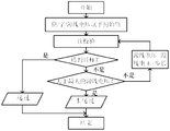
- FIG. 3 is a flow chart of a reset operation of a resistive memory
- FIG. 4 is a flowchart of a reset operation method of a resistive memory according to an embodiment of the present invention.
- FIG. 5 is a flow chart of a reset operation of a resistive memory with a transistor as a non-linear gate device according to an embodiment of the present invention
- FIG. 6 is a resistive memory device according to an embodiment of the present invention.
- FIG. 7 is a graph showing cumulative probability distribution results of memory cell resistance values in a resistive memory array using an existing reset method and a reset method of an embodiment of the present invention.
- a resistive memory includes, for example, a resistive memory array composed of memory cells based on a non-linear gate device and a resistive switching device.
- Figure 1 shows a resistive memory array.
- the resistive memory array is composed of, for example, eight word lines and 128 bit lines arranged alternately with each other.
- a memory cell is placed at the intersection of the bit line and the word line.
- Figure 2 shows the memory cell structure of a resistive memory array at the intersection, which is connected to the corresponding word line, source line and bit line.
- each memory cell includes a resistive switching element and a transistor. The gate of the transistor is connected to the word line, the source is connected to the source line, and the drain is connected in series to the bit line.
- the function of the word line is to apply a voltage to the transistor to turn the channel of the transistor on or off, thereby controlling the turn-on or turn-off of the transistor.
- a voltage may be applied to the resistive switching element in the memory cell through the source line and the bit line to set the resistance state of the resistive switching element.
- the structures of the resistive memory array and the memory unit shown in FIG. 1 and FIG. 2 are merely exemplary and are not intended to limit the present invention.
- the arrangement of rows and columns of memory cells in a memory array is not limited to the case shown in the figures.
- the non-linear gating device in the memory cell can also be a diode.
- the resistive switching element is a key component in the resistive memory array for storing data.
- the resistive element is, for example, a sandwich structure comprising a resistive layer in the middle and an electrode layer on both sides.
- the resistive layer can be, for example, a metal oxide or an organic material.
- the electrode layers on both sides of the resistive switching element can be respectively connected to the drain and bit lines of the transistor.
- the source of the transistor is connected to the source line and the gate is connected to the word line.
- a voltage is simultaneously applied to the bit line and the word line, for example, a set operation can be performed.
- a reset operation can be performed.
- the function of the gate of the transistor is to turn on the transistor by receiving the turn-on voltage from the word line.
- the channel is such that a voltage can be applied to the resistive layer through the electrodes on both sides of the resistive element. Therefore, in a structure using a transistor as a gate device, applying a voltage to the resistive layer requires opening the channel of the transistor first, that is, applying a turn-on voltage to the gate of the transistor through the word line.
- the resistance of the resistive element changes with the magnitude of the voltage applied across it, and there are two stages of low resistance and high resistance, including the two operations of set and reset.
- the reset operation is, for example, a process of applying a reset voltage to the resistive layer of the resistive variable element through electrodes on both sides of the resistive switching element, thereby gradually increasing the resistance of the resistive layer to enter a high resistance state.
- the set operation is, for example, a process of applying a set voltage opposite to the reset voltage to the resistive layer of the resistive switching element through electrodes on both sides of the resistive switching element, thereby causing the resistance of the resistive switching element to enter a low resistance state. It should be noted that the opposite direction of the reset voltage and the set voltage means that the direction of the electric field formed between the electrodes on both sides of the resistive switching element is different.
- Figure 3 illustrates a reset process for a resistive memory array.
- the resistive switching element of each memory cell is controlled by a transistor.
- the resistive memory array loading pulse is set as follows: after the reset of the resistive memory array is started, for example, the word line and the source line are applied to the memory cell of the resistive memory array to give an initial value of the voltage, that is, the source line end of the memory cell. And the word line terminal is loaded with a pulse voltage. Then, the read verify operation is performed, that is, the resistance value of the memory cell is obtained.
- the resistance value of the memory unit reaches the target resistance value. If the resistance of the memory cell is greater than or equal to the preset target resistance, the application of the pulse voltage to the memory cell is stopped, for example, the test pass may be determined as shown in FIG. 3, and the test is ended, that is, the application of the memory cell is stopped. Pulse voltage. If the resistance of the storage unit is less than the preset target resistance, further determining whether the voltage value of the storage unit is greater than the maximum voltage of the source line, and if so, stopping applying voltage to the storage unit, as shown in FIG.
- the function of the word line voltage is to open the channel of the transistor when the source line pulse is loaded.
- the starting source line voltage, the source line voltage step size, and the end point source line voltage are selected according to the characteristics of the resistive switching elements in the memory cell.
- the width of the word line pulse voltage and the source line pulse voltage are selected according to actual needs.
- the target resistance value is a resistance value of the memory cell in a high resistance state, and the target resistance value is determined according to characteristics of the memory array.
- the relaxation characteristic of the resistive memory has a great relationship with the erase programming operation mode.
- the resistance of the corresponding memory cell is abrupt.
- the sharply rising resistance causes the internal temperature of the resistive layer of the resistive memory to drastically decrease, so that the oxygen ions in the resistive layer move at a slower speed, and cannot effectively combine with oxygen vacancies to form a stable high-resistance state.
- the oxygen vacancies can capture the charge, which in turn forms an unstable high resistance value in the resistive layer of the resistive memory, resulting in a high-resistance fast relaxation phenomenon.
- embodiments of the present invention provide a method of operating a resistive memory and a resistive memory device.
- the resistive memory operating method of the present invention includes the steps of: applying an initial reset voltage to a memory cell in the resistive memory array; performing a read verify operation to obtain a resistance value of the memory cell; Whether the resistance value of the storage unit reaches a preset target resistance value; if the resistance value of the storage unit is greater than or equal to the target resistance value, ending the method; if the resistance value of the storage unit is smaller than the target a resistance value, a set voltage is applied to the memory cell to set the memory cell to a target resistance value in a low resistance state, and then a reset voltage of an increased amplitude is applied to the memory cell again, and The read verify operation and subsequent steps are repeated until the memory cell reaches the target resistance.
- the operation method of the resistive memory of the embodiment of the present invention first sets the memory cell to a low resistance state before a new reset voltage needs to be applied, thereby avoiding the memory cell due to the sharply rising resistance value during the reset process.
- the sharp rise of the device temperature can effectively suppress the high-resistance fast relaxation phenomenon and improve the data retention characteristics of the resistive memory.
- the resistive memory array can be preset with a target resistance value in a high resistance state.
- the target resistance should be the resistance that the memory cell can reach at the load voltage, and the target resistance is, for example, known.
- the same target resistance is set for each memory cell in the entire resistive memory array.
- the voltages that cause the respective memory cells to reach a high resistance state are, for example, not much different.
- the initial reset voltage applied to the resistive memory array is determined, for example, based on the voltage required to place the memory cell in a high impedance state. That is to say, the initial reset voltage setting should ensure that as many memory cells as possible reach the target resistance value, so as to improve the working efficiency of the resistive memory array and reduce the energy. Consumption.
- the setting operation of the resistive switching element also needs to ensure that the resistive switching element in each memory cell is not broken down.
- the target resistance of the memory cells in the low resistance state is, for example, a resistance value that can be achieved after applying a reverse set voltage to the memory cells, for example, setting the same target resistance value for each memory cell in the entire resistive memory array.
- the target resistance value of the memory cell in the low resistance state is not particularly limited as long as the memory cell is in a low resistance state after being applied with the set voltage and is not broken down.
- the target resistance value R1 of the resistive switching element in the memory cell in the low resistance state may be set to be slightly smaller than the resistance value R2 of the memory cell after the resistive switching element is activated. For example, R1 ⁇ 90% R2 to better improve the data retention characteristics of the resistive memory.
- R1 ⁇ 90% R2 to better improve the data retention characteristics of the resistive memory.
- the reset voltage applied to the memory cell after the initial reset voltage is typically set in an initial reset voltage plus step size.
- the amplitude of the reset voltage of the memory cell after the first set is the magnitude of the initial reset voltage plus the voltage value after one step, and so on.
- the voltage increase value is n steps, n ⁇ 1
- the setting of the step size needs to be based on the uniformity of the memory cells in the resistive memory. For example, if the uniformity of the memory cells is good, the step size can be set smaller.
- the step size can be set larger.
- the relationship between the step size h and the initial reset voltage Vs satisfies 0.02 Vs ⁇ h ⁇ 0.2 Vs to better alleviate the resistive relaxation phenomenon of the resistive memory.
- the non-linear gating device of the memory cell is, for example, a transistor.
- the reset voltage is applied through the word line terminal and the source line terminal of the memory cell, and the set voltage is applied through the word line terminal and the bit line terminal of the memory cell.
- the operating method of the resistive memory further includes the following steps: if the resistance of the memory cell is less than the target resistance, determining whether the reset voltage is greater than a maximum source line voltage, If not, a set voltage is applied to the memory cell, and if so, the method ends.
- the operating method of the resistive memory of the embodiment may further include: if the voltage of the memory cell is greater than the maximum source line voltage, determining that the memory cell test fails, ending the method.
- FIG. 5 is a flow chart showing a reset operation of a resistive memory in which a transistor is a non-linear gate device in one embodiment of the present invention.
- the resistive memory array first applies an initial reset voltage to the word line and the source line of the resistive memory array, that is, assigns a voltage initial value to the memory cell.
- the reset voltage is a pulse voltage
- the resistance value of the memory cell is obtained by a read verify operation, and it is determined whether the resistance value reaches a preset target resistance value. If the target resistance is reached, it is determined that the test passes, and the test is ended, that is, the application of, for example, a pulse voltage to these memory cells is stopped. If the memory cell does not reach the target resistance, it is further determined whether the voltage of the memory cell is greater than the magnitude of the source line voltage.
- the memory cells are set by applying, for example, a reverse set voltage to the word line and bit line terminals of the memory cells to set the memory cells to a target resistance in the low resistance state.
- the reset voltage is applied to the memory cell again according to the voltage and the step size of the source line, for example, the amplitude of the initial set voltage is increased by one step.
- the operation after the checksum is repeated is repeated until the resistance of the memory cell reaches the target resistance value, or the test is terminated because the voltage of the memory cell is greater than the magnitude of the source line voltage.
- the non-linear gating device in the memory cell is a transistor and the reset voltage is a pulse voltage applied through a word line terminal and a source line terminal of the memory cell.
- the initial reset voltage is a pulse voltage having a pulse width of 20-100 ns, for example, 40-60 ns, so that each memory cell can quickly reach a high-resistance state, reducing power consumption.
- the magnitude of the initial reset voltage should take into account the uniformity of the resistive memory array. That is, it should be ensured that after the initial reset voltage is applied, as many memory cells as possible reach the target resistance in the high resistance state. However, the amplitude of the pulse voltage should be no greater than the maximum of the threshold voltages of the memory cells in the resistive memory array.
- the initial reset voltage is a pulse voltage
- the amplitude of the pulse voltage is set to 60%
- the memory cell reaches a voltage value corresponding to the preset target resistance value to ensure more storage after the initial pulse voltage is applied.
- the cells reach their respective threshold voltages to avoid relaxation.
- the initial reset voltage is a pulse voltage
- the difference between the amplitude V max of the pulse voltage and the median V mid in the threshold voltage of the memory cell satisfies: -0.2 V ⁇ V max - V mid ⁇ 0.1 V, to ensure that More memory cells reach the preset target resistance after the initial reset voltage, avoiding relaxation.
- the read verify operation is to send a pulse voltage having an amplitude of 0.1-0.3 V to the memory cell, and acquire current data of the memory cell, and calculate the resistance value of the memory cell by the pulse voltage and the current data. .
- the pulse voltage of the read verify operation is set to 0.2-0.25 V, which further improves the detection accuracy of the resistance.
- the read verify operation is implemented, for example, by applying a pulse voltage on the word lines and bit lines of the resistive memory array.
- the non-linear gating device selected for the memory cell is a transistor.
- the set operation is implemented by applying a voltage to the bit line end of the memory cell. For example, for a resistive memory array using a transistor, for example, a pulse voltage is applied simultaneously at a word line terminal and a bit line terminal of a memory cell to implement a set operation.
- the set operation is increased, thereby avoiding the high-resistance fast relaxation phenomenon.
- the resistive relaxation of the resistive memory can be better avoided.
- the amplitude V2 of the set voltage applied to one memory cell and the amplitude V1 of the reset voltage applied to the memory cell before being set satisfies -0.4 ⁇ V2 - V1 ⁇ 0.
- the amplitude V2 of the set voltage applied to one memory cell and the amplitude V1 of the reset voltage applied to the memory cell before being set satisfies -0.2 ⁇ V2 - V1 ⁇ 0 to further reduce the resistance of the memory. Resistance state relaxation.
- the target resistance of the memory cell in the low resistance state in the set operation is also realized by cyclically loading the pulse voltage on the memory cell after setting the initial value of the voltage and the step size.
- the reading of the resistance of the memory cell also needs to use the read verify judgment, that is, obtain the current value of the memory cell, and calculate the resistance value of the memory cell in combination with the voltage applied to the memory cell. And according to the calculated resistance value of the memory cell, performing the operation of continuously applying the pulse voltage or stopping the application of the pulse voltage.
- the device includes a resistive memory array, a control module, and a test module.
- the control module sends an instruction to the test module to apply a reset voltage to a memory cell in the resistive memory array, and the test module is controlled to apply a reset voltage to the memory cell.
- the control module acquires the resistance value of the storage unit, compares the obtained resistance value of the storage unit with a preset target resistance value, and performs the following steps according to the comparison result:
- the control module sends an instruction to apply the set voltage to the test module, and the test module is controlled to apply a set voltage to the storage unit to
- the memory cell is set to a target resistance value in a low resistance state; the control module sends a reset voltage command applying an amplitude increase to the test module, and controlling the test module to apply an amplitude increase to the memory unit
- the control module and the test module repeat the above-mentioned steps of acquiring the resistance of the memory cell and the subsequent steps until the resistance of the memory cell is greater than or equal to the target resistance.
- the control module controls the test module to stop applying a reset voltage to the memory cell if the resistance of the memory cell is greater than or equal to a target value.
- the memory cell includes a resistive switching element and a non-linear gating device, the non-linear gating device is a transistor; a reset voltage is applied through a word line terminal and a source line terminal of the memory cell, and the set voltage is passed through the storage The word line end and the bit line end of the unit are applied.
- control module and the test module may further perform the following operations: if the resistance of the storage unit is less than the target resistance, the control module determines whether the reset voltage is greater than a maximum source line voltage, and if not, controls The module control test module applies a set voltage to the memory unit, and if so, the control module controls the test module to stop applying a voltage to the memory unit; if the reset voltage is greater than the maximum source line voltage, the control module determines that the memory unit test is not Pass and end the test.
- FIG. 6 shows a resistive memory device in accordance with an embodiment of the present invention.
- the control module is, for example, a computing device of a computer
- the test module is, for example, an array tester.
- the computer can set various parameters, such as inputting a preset target resistance value, setting a reset voltage and a set voltage (a reset voltage and a set voltage, for example, a pulse voltage), and setting a read verify pulse voltage, etc.
- the test machine sends an execution instruction; the array test machine sends, for example, a pulse voltage to the resistive memory array sample, and acquires relevant data (eg, current data) of each storage unit in the resistive memory array to transmit the data to the computer;
- the data is processed correspondingly and the next operation is determined, for example, the memory cell resistance value and the target resistance value are compared, and the operation of setting the memory cell or stopping the application of the pulse voltage to the memory cell is determined according to the comparison result.
- control module obtains the resistance value of the storage unit by: the control module controls the test module to send a pulse voltage with an amplitude of 0.1-0.3V to the storage unit; and the test module collects the current of the storage unit in the resistive memory array. Data, the collected current data is transmitted to the control module; the control module calculates the resistance of each storage unit by the pulse voltage and the collected current data value.
- control module controls the amplitude of the pulse voltage sent by the test module to the storage unit to be 0.2-0.25 V to further improve the detection accuracy and avoid circuit crosstalk.
- the non-linear gating device of the memory cell can be a transistor or a diode.
- the resistive memory device of the embodiment of the present invention may include a resistive memory array, a control module, and a test module.
- the control module can include an input/output (I/O) interface that allows the operator to make the above parameter settings through the interface.
- the test module can, for example, perform corresponding operations in accordance with the instructions of the received control module, such as providing an initial pulse voltage or the like.
- the control module and the test module are not necessarily independent modules, as long as they have the functions described above.
- the structure of the memory array to be tested is the structure shown in FIG. That is, the resistive memory array includes eight word lines/source lines and 128 bit lines, and is a memory cell at the intersection of each word line/source line and bit line.
- the structure of each memory cell of the resistive memory array is as shown in FIG. 2. That is, the memory cell includes, for example, a resistive switching element and a transistor. The gate of the transistor is connected to the word line, the source is connected to the source line, and the drain is connected in series with a resistive memory and connected to the bit line.
- the resetting operation of the resistive memory array is performed using the reset method shown in FIG. 3 and the reset method of the embodiment of the present invention as shown in FIG. 5, respectively.
- the resistance of each memory cell in the initial state of the resistive memory array and the resistance after heating at 175 ° C for 2 hours are tested.
- FIG. 7 is a graph showing cumulative probability distribution results of memory cell resistance values in a resistive memory array using the reset method shown in FIG. 3 and the reset method of the embodiment of the present invention as shown in FIG. 5.
- the abscissa in Figure 7 is the resistance value of each memory cell in the resistive memory array, in ohms ( ⁇ ); the ordinate is the cumulative probability distribution of the memory cells in the resistive memory array.
- R11 and R12 in the figure respectively indicate cumulative probability distribution lines of the resistance values of the memory cells before and after heating using the existing reset method.
- R21 in the figure and R22 in the figure respectively indicate cumulative probability distribution lines of the resistance values of the memory cells before and after heating using the reset method of the embodiment of the present invention.
- the 200k ⁇ in the figure is the target resistance set for the resistive memory.
- the resistive memory device of the present invention can be implemented by means of software, firmware and necessary general hardware, and can also be implemented by dedicated hardware, but in many cases, the former may be preferred.
- the technical solution of the present invention is embodied in the form of software, hardware, firmware or any combination thereof, wherein the software product involved is stored in a readable storage medium, such as a magnetic storage medium (such as a hard disk). Or an electronic storage medium (e.g., ROM, flash memory) or the like, including instructions for causing a device (which may be a computer, server or network device, etc.) to perform the methods described in various embodiments of the present invention.
Landscapes
- Semiconductor Memories (AREA)
Abstract
一种阻变存储器的操作方法及阻变存储器装置。该方法包括如下步骤:对阻变存储器阵列中的存储单元施加初始重置电压;进行读校验操作,以获取所述存储单元的阻值;判断所述存储单元的所述阻值是否达到预设的目标阻值;如果所述存储单元的阻值大于等于所述目标阻值,则结束所述方法;如果所述存储单元的阻值小于所述目标阻值,则向所述存储单元施加置位电压,以将所述存储单元置位到在低阻态的目标阻值,然后对所述存储单元再次施加幅值升高的重置电压,并重复所述读校验操作及之后的步骤,直到所述存储单元达到所述目标阻值。可有效缓解阻变存储器的高阻态快速弛豫现象。
Description
本发明的实施例涉及一种阻变存储器的操作方法和阻变存储器装置。
阻变式存储器(RRAM)由于速度快、容量大及功耗低等优点,而成为下一代非易失性存储技术的研究热点。
阻变式存储器的数据保持能力,是判断其性能的重要指标之一。对阻变式存储器进行擦写操作之后,在短时间内,其阻值会出现一个快速减小的过程。这种现象被称为阻变式存储器的阻态弛豫特性。阻态弛豫特性会严重影响阻态的数据保持特性,使得高低阻值的窗口缩小甚至消失,进而导致阻变式存储器器件的功能失效。
发明内容
本发明实施例提供了一种阻变存储器的操作方法,包括如下步骤:对阻变存储器阵列中的存储单元施加初始重置电压;进行读校验操作,以获取所述存储单元的阻值;判断所述存储单元的所述阻值是否达到预设的目标阻值;如果所述存储单元的阻值大于等于所述目标阻值,则结束所述方法;如果所述存储单元的阻值小于所述目标阻值,则向所述存储单元施加置位电压,以将所述存储单元置位到在低阻态的目标阻值,然后对所述存储单元再次施加幅值升高的重置电压,并重复所述读校验操作及之后的步骤,直到所述存储单元达到所述目标阻值。
在本发明的实施例中,例如,所述存储单元包括阻变元件和非线性选通器件,所述非线性选通器件为晶体管,所述重置电压通过所述存储单元的字线端和源线端施加。
在本发明的实施例中,例如,如果所述存储单元的阻值小于所述目标阻值,则判断所述重置电压是否大于最大的源线电压,如果不是,则向所述存储单元施加置位电压,如果是,则结束所述方法。
在本发明的实施例中,例如,如果存储单元的电压大于最大源线电压,则判定该存储单元测试不通过,结束所述方法。
在本发明的实施例中,例如,所述幅值升高的重置电压等于源线电压与步长之和。
在本发明的实施例中,例如,所述初始重置电压为脉冲电压,该脉冲电压的脉冲宽度为20-100ns。
在本发明的实施例中,例如,所述脉冲电压的脉冲宽度为40-60ns。
在本发明的实施例中,例如,所述阻变存储器阵列中包括多个所述存储单元;所述初始重置电压为脉冲电压,所述脉冲电压的幅值不大于多个所述存储单元的临界电压中的最大值。
在本发明的实施例中,例如,所述阻变存储器阵列中包括多个所述存储单元;所述初始重置电压为脉冲电压,所述脉冲电压的幅值Vmax与多个所述存储单元的临界电压中的中位数Vmid之差满足:-0.2V≤Vmax-Vmid≤0.1V。
在本发明的实施例中,例如,所述读校验操作为向所述存储单元发送幅值为0.1-0.3V的脉冲电压,并获取所述存储单元的电流数据,通过该脉冲电压和所述电流数据计算所述存储单元的阻值。
在本发明的实施例中,例如,所述读校验操作为向所述存储单元发送幅值为0.2-0.25V的脉冲电压。
在本发明的实施例中,例如,所述存储单元包括阻变元件和非线性选通器件,所述非线性选通器件为晶体管,所述置位电压在所述存储单元的字线端和位线端施加。
在本发明的实施例中,例如,对所述存储单元施加的置位电压的幅值V2与对该存储单元在置位前施加的重置电压的幅值V1满足-0.4≤V2-V1<0。
在本发明的实施例中,例如,对所述存储单元施加的置位电压的幅值V2与对该存储单元在置位前施加的重置电压的幅值V1满足-0.2≤V2-V1<0。
在本发明的实施例中,例如,如果所述存储单元的阻值等于预设的目标阻值,则判定所述存储单元测试通过,然后结束所述方法。
本发明的实施例提供了一种阻变存储器装置,包括阻变存储器阵列、控制模块和测试模块;所述控制模块控制所述测试模块向所述阻变存储器阵列中的存储单元施加重置电压;所述控制模块获取所述存储单元的阻值,并将
所获取的所述存储单元的阻值与预设的目标阻值比较,根据比较结果,进行以下步骤:如果所述存储单元的阻值小于所述目标阻值,则所述控制模块控制所述测试模块向所述存储单元施加置位电压,以将所述存储单元置位到在低阻态的目标阻值;所述控制模块控制所述测试模块向所述存储单元施加幅值增加的所述重置电压;所述控制模块及所述测试模块重复上述获取所述存储单元阻值以及之后的步骤,直至所述存储单元的阻值等于目标阻值;如果所述存储单元的阻值大于等于目标值,所述控制模块控制所述测试模块停止向所述存储单元施加重置电压。
在本发明的实施例中,例如,所述存储单元包括阻变元件和非线性选通器件,所述非线性选通器件为晶体管;所述重置电压通过所述存储单元的字线端和源线端施加,所述置位电压通过所述存储单元的字线端和位线端施加。
在本发明的实施例中,例如,如果所述存储单元的阻值小于所述目标阻值,则所述控制模块判断所述重置电压是否大于最大的源线电压,如果不是,则所述控制模块控制所述测试模块向所述存储单元施加置位电压,如果是,则所述控制模块控制所述测试模块停止向所述存储单元施加电压。
在本发明的实施例中,例如,所述重置电压大于最大的源线电压,则控制模块判定该存储单元测试不通过,并结束测试。
在本发明的实施例中,例如,所述非线性选通器件为晶体管或二极管。
为了更清楚地说明本实用新型实施例的技术方案,下面将对实施例的附图作简单地介绍,显而易见地,下面描述中的附图仅仅涉及本实用新型的一些实施例,而非对本实用新型的限制。
图1为一种阻变存储器阵列结构示意图;
图2为一种阻变存储器阵列中的存储单元结构示意图;
图3为阻变存储器的复位操作的流程图;
图4为本发明实施例阻变存储器的复位操作方法流程图;
图5为本发明实施例中阻变存储器以晶体管为非线性选通器件的复位操作的流程图;
图6为本发明实施例的一种阻变存储器装置;
图7为采用现有复位方法和本发明实施例的复位方法的阻变存储器阵列中存储单元阻值的累积概率分布结果图。
为使本发明的目的、技术方案和优点更加清楚,下面将结合本发明实施例的附图,对本发明实施例的技术方案进行清楚、完整地描述。显然,所描述的实施例是本发明的一部分实施例,而不是全部的实施例。基于所描述的本发明的实施例,本领域普通技术人员在无需创造性劳动的前提下所获得的所有其他实施例,都属于本发明保护的范围。
目前,阻变存储器例如包括以非线性选通器件和阻变元件为基础的存储单元构成的阻变储器阵列。图1示出了一种阻变存储器阵列。参照图1,阻变存储器阵列例如由彼此交叉排布的8条字线和128条位线组成。在位线与字线的交叉点设置一个存储单元。图2示出了交叉点处阻变存储器阵列的存储单元结构,该存储单元连接到相应的字线、源线和位线。参照图2,每一个存储单元包括一个阻变元件和一个晶体管。晶体管的栅极与字线连接,源极与源线连接,漏极串联阻变元件后连接至位线。字线的作用是对晶体管施加电压,以将晶体管的沟道打开或关闭,从而控制晶体管的导通或截止。在晶体管导通后,例如,可以通过源线和位线向存储单元中的阻变元件施加电压,以设置该阻变元件的阻态。
需要说明的是,图1和图2所示的阻变存储器阵列及存储单元的结构仅是示例性的,并非对本发明的限制。例如,存储阵列中存储单元的行与列的布置不限于图中示出的情形。例如,存储单元中的非线性选通器件也可以为二极管。
阻变元件是阻变式存储器阵列中用于存储数据的关键部件。一般来讲,阻变元件例如为夹心结构,包括位于中间的阻变层和位于两侧的电极层。阻变层例如可以是金属氧化物或者有机材料。例如采用晶体管作为阻变存储器的选通器件时,阻变元件的两侧的电极层可以分别连接晶体管的漏极和位线。晶体管的源极连接源线,栅极连接字线。这样,在位线和字线同时施加电压时,例如可以进行置位操作。在源线和字线施加电压时,例如可以进行复位操作。晶体管的栅极的作用是通过接收来自字线的导通电压而打开晶体管的
沟道,从而可以通过阻变元件两侧电极向阻变层施加电压。因此,在采用晶体管作为选通器件的结构中,对阻变层施加电压均需要先打开晶体管的沟道,也即需要通过字线对晶体管的栅极施加导通电压。
阻变元件的阻值随着施加在其两端的电压大小而变化,会出现低阻态和高阻态两个阶段,即包括置位和复位两个操作过程。复位操作例如是通过阻变元件两侧的电极向阻变元件的阻变层施加重置电压,而使该阻变层的电阻逐渐增加以致进入高阻态的过程。置位操作例如是通过阻变元件两侧的电极向阻变元件的阻变层施加与重置电压相反的置位电压,而使阻变元件的电阻进入低阻态的过程。需要说明的是,重置电压与置位电压方向相反是指阻变元件两侧电极之间所形成的电场方向不同。
目前,阻变存储器阵列的擦写编程大多采用逐步增加的脉冲编程算法。图3示出了阻变存储器阵列的一种复位过程。图3所示的阻变存储器阵列中,每个存储单元的阻变元件通过晶体管控制。参照图3,阻变存储器阵列加载脉冲的设置方式如下:阻变存储器阵列复位开始后,例如在字线和源线对阻变存储器阵列的存储单元赋予电压初始值,即存储单元的源线端和字线端加载脉冲电压。随后进行读校验操作,即获取存储单元的阻值。然后判断存储单元的阻值是否达到目标阻值。如果存储单元的阻值大于等于预设的目标阻值,则停止对该存储单元施加脉冲电压,例如可以是如图3中所示判定测试通过,并结束测试,也即停止对该存储单元施加脉冲电压。如果存储单元的阻值小于预设的目标阻值,则进一步判断存储单元的电压值是否大于源线最大电压,如果是,则停止对该存储单元施加电压,如图3所示判定未通过测试,之后结束测试,也即停止对该存储单元施加脉冲电压;如果不是,则增加电压幅值后(一般是采用初始电压加步长的方式)通过源线对该存储单元继续加载脉冲电压,并重复读校验及之后的操作,直至存储单元的阻值达到目标值或以其他方式结束测试。
需要说明的是,在阻变存储器阵列的复位过程中,字线电压的作用是在加载源线脉冲时打开晶体管的沟道。起始源线电压、源线电压步长以及终点源线电压根据存储单元中阻变元件的特性选择。字线脉冲电压和源线脉冲电压的宽度根据实际需要选择。上述目标阻值为存储单元处于高阻态的阻值,该目标阻值根据存储器阵列的特性确定。
对于采用上述算法对阻变存储器阵列中每一个存储单元进行复位编程的操作,发明人注意到,阻变存储器的弛豫特性与擦写编程操作方式有很大的关系。当源线脉冲幅值增加到临界电压脉冲前后,相应的存储单元的阻值发生突变。急剧升高的阻值导致阻变存储器的阻变层内部温度急剧降低,从而使得阻变层里的氧离子移动速度变慢,无法与氧空位有效复合形成稳定的高阻态。与此同时,氧空位能够捕获电荷,进而在阻变存储器的阻变层里形成不稳定的高阻值,造成高阻态快速弛豫现象。
针对上述高阻态快速弛豫现象,本发明的实施例提供了阻变存储器的操作方法和阻变存储器装置。
本发明实施例的一个方面提供了一种阻变存储器的操作方法。参照图4,本发明的阻变存储器操作方法包括如下步骤:对阻变存储器阵列中的存储单元施加初始重置电压;进行读校验操作,以获取所述存储单元的阻值;判断所述存储单元的所述阻值是否达到预设的目标阻值;如果所述存储单元的阻值大于等于所述目标阻值,则结束所述方法;如果所述存储单元的阻值小于所述目标阻值,则向所述存储单元施加置位电压,以将所述存储单元置位到在低阻态的目标阻值,然后对所述存储单元再次施加幅值升高的重置电压,并重复所述读校验操作及之后的步骤,直到所述存储单元达到所述目标阻值。
本发明实施例的阻变存储器的操作方法,在需要施加新的重置电压之前,先将存储单元置位到在低阻态,避免了重置过程中存储单元由于急剧升高的阻值导致器件温度的急剧上升,可以有效抑制高阻态快速弛豫现象,提高阻变存储器的数据保持特性。
需要说明的是,在对阻变存储器阵列中的存储单元施加重置电压之前,例如可以对阻变存储器阵列预设一个在高阻态的目标阻值。该目标阻值应为存储单元在加载电压下可以达到的阻值,且该目标阻值例如是已知的。例如,对整个阻变存储器阵列中的各存储单元设定同一个目标阻值。一般来讲,对于同一个阻变存储器阵列而言,使各个存储单元达到高阻态的电压例如相差不大。
另外,对阻变存储器阵列施加的初始重置电压例如是根据使存储单元处于高阻态所需的电压而确定。也就是说,初始重置电压的设置应该保证尽可能多的存储单元达到目标阻值,以提高阻变存储器阵列的工作效率,减小能
耗。
对阻变元件的置位操作例如也需要确保各存储单元中的阻变元件不被击穿。这些存储单元在低阻态的目标阻值例如也是对存储单元施加反向置位电压后可达到的阻值,例如对整个阻变存储器阵列中的各存储单元设定同一个目标阻值。本发明的实施例中,对存储单元在低阻态的目标阻值并不特别限定,只要保证存储单元在被施加置位电压后处于低阻态且不被击穿即可。在设置存储单元在低阻态的目标值时,例如可以将存储单元中阻变元件在低阻态的目标阻值R1设置为略小于该存储单元中阻变元件被激活后的阻值R2。例如R1≥90%R2,以更好的提高阻变存储器的数据保持特性。通过增加反向置位操作,避免了各存储单元的电压处于各自临界电压附近,提高阻变存储器阵列的数据保持特性。
在初始重置电压之后对存储单元施加的重置电压一般以初始重置电压加步长的方式设置。例如,在第一次置位后对存储单元的重置电压的幅值为初始重置电压的幅值加一个步长后的电压值,依次类推。通过对未达到目标阻值的存储单元施加逐渐增加重置电压(例如每一次循环后增加一个步长,即电压增加值为n个步长,n≥1),以使更多的存储单元达到在高阻态的目标阻值。步长的设置需要根据阻变存储器中存储单元的均一性而定,例如存储单元的均一性好,则可以将步长设置的更小。相反地,如果存储单元之间的均一性较差,可以将步长设置的大一些。例如,步长h与初始重置电压Vs的关系满足0.02Vs≤h≤0.2Vs,以更好的缓解阻变存储器的阻态弛豫现象。
在一个实施例中,存储单元的非线性选通器件例如为晶体管。重置电压通过存储单元的字线端和源线端施加,置位电压通过所述存储单元的字线端和位线端施加。在该实施例中,进一步地,阻变存储器的操作方法还包括如下步骤:如果所述存储单元的阻值小于所述目标阻值,则判断所述重置电压是否大于最大的源线电压,如果不是,则向所述存储单元施加置位电压,如果是,则结束所述方法。例如,进一步地,该实施例的阻变存储器的操作方法还可以包括:如果存储单元的电压大于最大源线电压,则判定该存储单元测试不通过,结束所述方法。
图5示出了本发明一个实施例中以晶体管为非线性选通器件的阻变存储器的复位操作流程图。
参照图5,阻变存储器阵列在复位操作开始后,首先在阻变存储器阵列的字线和源线施加初始重置电压,即对存储单元赋予电压初值。例如该重置电压为一个脉冲电压;随后,通过读校验操作获取该存储单元的阻值,并判断该阻值是否达到预设的目标阻值。如果达到目标阻值,则判定测试通过,并结束测试,即停止向这些存储单元施加例如脉冲电压。如果存储单元没有达到目标阻值,则进一步判断存储单元的电压是否大于源线电压的幅值。如果是,则判定测试未通过,并停止对该存储单元施加例如脉冲电压。如果不是,则通过对这些存储单元的字线端和位线端施加例如反向置位电压对该存储单元进行置位操作,以将这些存储单元置位到在低阻态的一个目标阻值;之后,根据源线的电压和步长,例如初始置位电压的幅值增加一个步长后的电压,对存储单元再次施加重置电压。重复读校验及之后的操作,直至存储单元的阻值达到目标阻值为止,或由于存储单元的电压是否大于源线电压的幅值而结束测试。
在一个实施例中,存储单元中的非线性选通器件为晶体管,重置电压为通过存储单元的字线端和源线端施加的脉冲电压。
例如,初始重置电压为脉冲电压,该脉冲电压的脉冲宽度为20-100ns,例如为40-60ns,以使各存储单元能够快速到达高阻态,减小能耗。
初始重置电压的幅值应当考虑阻变存储器阵列的均一性。即应当保证在该初始重置电压施加后,有尽可能多的存储单元达到在高阻态的目标阻值。但该脉冲电压的幅值应不大于阻变存储器阵列中各存储单元的临界电压中的最大值。
例如,初始重置电压为脉冲电压,该脉冲电压的幅值设置为60%的存储单元达到预设目标阻值所对应的电压值,以保证在施加该初始脉冲电压后,有更多的存储单元达到各自的临界电压,避免弛豫现象。
例如,初始重置电压为脉冲电压,该脉冲电压的幅值Vmax与存储单元临界电压中的中位数Vmid之差满足:-0.2V≤Vmax-Vmid≤0.1V,以保证有更多的存储单元在初始重置电压之后达到预设目标阻值,避免弛豫现象。
在一个实施例中,读校验操作为向存储单元发送一个幅值为0.1-0.3V的脉冲电压,并获取存储单元的电流数据,通过该脉冲电压和所述电流数据计算存储单元的阻值。在进行读校验操作时,如果脉冲电压过小,则无法准确
测量各个存储单元的阻值;如果脉冲电压过大,则有可能会发生电路串扰。因此,通过将读校验操作的脉冲电压设置在0.1-0.3V,既可准确测量各个存储单元的阻值,又能有效防止电路串扰。例如,该读校验的脉冲电压设置为0.2-0.25V,进一步提高阻值的检测精度。通过精确测量存储器阵列中各存储单元的阻值,为后续步骤打下基础,以更好的避免弛豫现象。
需要说明的是,对于以晶体管为开关的阻变存储器阵列而言,读校验操作例如是在阻变存储器阵列的字线和位线上施加脉冲电压实现的。
在一个实施例中,存储单元选用的非线性选通器件为晶体管。置位操作的实现方式为在存储单元的位线端施加电压。例如对于采用晶体管的阻变存储器阵列而言,在存储单元的字线端和位线端同时施加例如脉冲电压,以实现置位操作。本发明的实施例中,对于经过初始置位电压后未达到预设目标阻值的存储单元,增加了置位操作,从而更好的避免了高阻态快速弛豫现象。
在一个实施例中,通过调整置位操作中置位电压幅值与重置电压幅值的关系,可以更好的避免阻变存储器的阻态弛豫现象。例如,对一个存储单元施加的置位电压的幅值V2与对该存储单元在置位前施加的重置电压的幅值V1满足-0.4≤V2-V1<0。例如,对一个存储单元施加的置位电压的幅值V2与对该存储单元在置位前施加的重置电压的幅值V1满足-0.2≤V2-V1<0,以进一步降低阻变存储器的阻态弛豫。
需要指出的是,置位操作中存储单元在低阻态的目标阻值也是通过设置电压初值及步长后,对存储单元循环加载脉冲电压而实现的。这里,存储单元阻值的读取也需要采用读校验判断,即获取存储单元的电流值,并结合施加到该存储单元的电压计算出该存储单元的阻值。并根据计算出的存储单元的阻值,执行继续施加脉冲电压或者停止施加脉冲电压操作。
本发明实施例的另一个方面提供了一种阻变存储器阵列装置,可有效缓解阻变存储器阵列中阻变存储器的阻态弛豫现象。该装置备包括阻变存储器阵列、控制模块和测试模块。
所述控制模块向所述测试模块发送向阻变存储器阵列中的存储单元施加重置电压的指令,控制所述测试模块向所述存储单元施加重置电压。
所述控制模块获取所述存储单元的阻值,并将所获取的所述存储单元的阻值与预设的目标阻值比较,根据比较结果,进行以下步骤:
如果所述存储单元的阻值小于所述目标阻值,则所述控制模块向所述测试模块发送施加置位电压的指令,控制所述测试模块向所述存储单元施加置位电压,以将所述存储单元置位到在低阻态的目标阻值;所述控制模块向所述测试模块发送施加幅值增加的重置电压指令,控制所述测试模块向所述存储单元施加幅值增加的所述重置电压;所述控制模块及所述测试模块重复上述获取所述存储单元阻值以及之后的步骤,直至所述存储单元的阻值大于等于目标阻值。
如果所述存储单元的阻值大于等于目标值,所述控制模块控制所述测试模块停止向所述存储单元施加重置电压。
在一个实施例中,存储单元包括阻变元件和非线性选通器件,非线性选通器件为晶体管;重置电压通过存储单元的字线端和源线端施加,置位电压通过所述存储单元的字线端和位线端施加。在该实施例中,控制模块和测试模块还可进行如下操作:如果存储单元的阻值小于目标阻值,则控制模块判断所述重置电压是否大于最大的源线电压,如果不是,则控制模块控制测试模块向存储单元施加置位电压,如果是,则控制模块控制测试模块停止向所述存储单元施加电压;如果重置电压大于最大的源线电压,则控制模块判定该存储单元测试不通过,并结束测试。
图6示出了本发明实施例的一种阻变存储器装置。参照图6,控制模块例如为一台电脑的计算设备,测试模块例如为一台阵列测试机。电脑可以设置各种参数,例如输入预设目标阻值,设定重置电压及置位电压(重置电压和置位电压例如为脉冲电压)以及设定读校验脉冲电压等,并向阵列测试机发送执行指令;阵列测试机向阻变存储器阵列样品发送例如脉冲电压,并获取阻变存储器阵列中各存储单元的相关数据(例如电流数据),以将数据传输给电脑;电脑例如根据这些数据进行相应的处理和确定下一步操作等,例如比较存储单元阻值和目标阻值,并根据比较结果确定对存储单元进行置位或停止对存储单元施加脉冲电压等操作。
需要说明的是,控制模块获取存储单元阻值的方式可以为:控制模块控制测试模块向存储单元发送一个幅值为0.1-0.3V的脉冲电压;测试模块采集阻变存储器阵列中存储单元的电流数据,将所采集到的电流数据传输给控制模块;控制模块通过该脉冲电压以及所采集的电流数据计算各存储单元的阻
值。
例如,控制模块控制测试模块向存储单元发送的脉冲电压的幅值可以为0.2-0.25V,以进一步提高检测精度,避免发生电路串扰。
在一个实施例中,存储单元的非线性选通器件可以为晶体管或二极管。
本领域技术人员可知:本发明实施例的阻变存储器装置可以包括阻变存储器阵列、控制模块和测试模块。例如控制模块可以包括一个输入/输出(I/O)界面,操作人员可以通过界面进行上述参数设定。测试模块例如可以按照所接收到的控制模块的指令执行相应操作,例如提供初始脉冲电压等。控制模块和测试模块并不一定是彼此独立的模块,只要具备如上所述的功能即可。
本公开的发明人通过实验进行了验证本发明实施例的技术效果,具体如下所述。
待测的存储器阵列结构图均为图1所示的结构。即阻变存储器阵列包括8条字线/源线和128条位线,在每一条条字线/源线和位线的交叉点为一个存储单元。阻变存储器阵列的每个存储单元的结构如图2所示。即存储单元例如包括一个阻变元件和一个晶体管。晶体管的栅极与字线连接,源极与源线连接,漏极串联一个阻变存储器后连接到位线。
实验时,分别使用图3所示的复位方法以及如图5所示的本发明实施例的复位方法对阻变存储器阵列进行复位操作。阻变存储器阵列复位操作完成后,测试阻变存储器阵列的初始状态各存储单元的阻值和在175℃下加热2小时后的阻值。
图7为采用图3所示的复位方法和如图5所示的本发明实施例的复位方法的阻变存储器阵列中存储单元阻值的累积概率分布结果图。图7中的横坐标为阻变存储器阵列中各存储单元的电阻值,单位为欧姆(Ω);纵坐标为阻变存储器阵列中存储单元的累积概率分布。图中R11和R12分别指示采用现有复位方法在加热前后存储单元的阻值的累积概率分布线。图中R21和图中R22分别指示采用本发明实施例的复位方法在加热前后存储单元阻值的累积概率分布线。图中的200kΩ为对阻变存储器设定的目标阻值。
参照图7可知,采用图3所示的复位方法进行阻变存储器阵列的复位操作后,约有10%的存储单元的阻值达不到目标阻值,且部分存储单元的阻值低于100KΩ;在加热2小时后,已经有70%以上的存储单元的阻值小于目标
阻值。部分存储单元的阻值已经下降到目标阻值的10倍以上,导致10倍的高低阻值窗口消失,即部分阻变元件失效。而在同等条件下,采用图5所示的本发明实施例的方法对阻变存储器阵列进行复位操作后,几乎所有存储单元的阻值都大于目标阻值200KΩ。此外,继续参照图5,在加热2小时后,仅有2%左右的存储单元的阻值小于目标阻值200KΩ,且这些存储单元的阻值也接近200KΩ。由此,可知,采用本发明的实施例的复位方法,可明显提高阻变存储器阵列的数据保持能力。
需要指出的是,上述实验条件及结果仅是为了说明本发明实施例提高阻变存储器数据保持能力的效果,而并非对本发明的限制。本领域技术人员可知,在不脱离本发明实质内涵的前提下改变上述实验条件时,仍然可以得到能够证明本发明效果的结论。
所属领域的技术人员可以清楚地了解到本发明的阻变存储器装置可借助软件、固件加必需的通用硬件的方式来实现,当然也可以通过专用的硬件来实现,但很多情况下前者可能是优选的实施方式。基于这样的理解,本发明的技术方案本质上以软件、硬件、固件或它们的任意组合的方式体现,其中所涉及的软件产品存储在可读取的存储介质中,如磁性存储介质(例如硬盘)或电子存储介质(例如ROM、闪存)等,包括若干指令用以使得一台设备(可以是计算机、服务器或者网络设备等)执行本发明各个实施例所述的方法。
以上所述仅是本发明的示范性实施方式,而非用于限制本发明的保护范围,本发明的保护范围由所附的权利要求确定。
本申请要求于2016年1月22日递交的第201610045713.9号中国专利申请的优先权,在此全文引用上述中国专利申请公开的内容以作为本申请的一部分。
Claims (20)
- 一种阻变存储器的操作方法,包括如下步骤:对阻变存储器阵列中的存储单元施加初始重置电压;进行读校验操作,以获取所述存储单元的阻值;判断所述存储单元的所述阻值是否达到预设的目标阻值;如果所述存储单元的阻值大于等于所述目标阻值,则结束所述方法;如果所述存储单元的阻值小于所述目标阻值,则向所述存储单元施加置位电压,以将所述存储单元置位到在低阻态的目标阻值,然后对所述存储单元再次施加幅值升高的重置电压,并重复所述读校验操作及之后的步骤,直到所述存储单元达到所述目标阻值。
- 根据权利要求1所述的阻变存储器的操作方法,其中,所述存储单元包括阻变元件和非线性选通器件,所述非线性选通器件为晶体管,所述重置电压通过所述存储单元的字线端和源线端施加。
- 根据权利要求2所述的阻变存储器的操作方法,其中,如果所述存储单元的阻值小于所述目标阻值,则判断所述重置电压是否大于最大的源线电压,如果不是,则向所述存储单元施加置位电压,如果是,则结束所述方法。
- 根据权利要求3所述的阻变存储器的操作方法,其中,如果存储单元的电压大于最大源线电压,则判定该存储单元测试不通过,然后结束所述方法。
- 根据权利要求2所述的阻变存储器的操作方法,其中,所述幅值升高的重置电压等于源线电压与步长之和。
- 根据权利要求1所述的阻变存储器的操作方法,其中,所述初始重置电压为脉冲电压,该脉冲电压的脉冲宽度为20-100ns。
- 根据权利要求6所述的阻变存储器的操作方法,其中,所述脉冲电压的脉冲宽度为40-60ns。
- 根据权利要求1所述的阻变存储器的操作方法,其中,所述阻变存储器阵列包括多个所述存储单元;所述初始重置电压为脉冲电压,所述脉冲电压的幅值不大于多个所述存储单元的临界电压中的最大值。
- 根据权利要求1所述的阻变存储器的操作方法,其中,所述阻变存储 器阵列中包括多个所述存储单元;所述初始重置电压为脉冲电压,所述脉冲电压的幅值Vmax与多个所述存储单元的临界电压中的中位数Vmid之差满足:-0.2V≤Vmax-Vmid≤0.1V。
- 根据权利要求1-9任意一项所述的阻变存储器的操作方法,其中,所述读校验操作为向所述存储单元发送幅值为0.1-0.3V的脉冲电压,并获取所述存储单元的电流数据,通过该脉冲电压和所述电流数据计算所述存储单元的阻值。
- 根据权利要求10所述的阻变存储器的操作方法,其中,所述读校验操作为向所述存储单元发送幅值为0.2-0.25V的脉冲电压。
- 根据权利要求1-9任意一项所述的阻变存储器的操作方法,其中,所述存储单元包括阻变元件和非线性选通器件,所述非线性选通器件为晶体管,所述置位电压在所述存储单元的字线端和位线端施加。
- 根据权利要求1-9任意一项所述的阻变存储器的操作方法,其中,对所述存储单元施加的置位电压的幅值V2与对该存储单元在置位前施加的重置电压的幅值V1满足-0.4≤V2-V1<0。
- 根据权利要求13所述的阻变存储器的操作方法,其中,对所述存储单元施加的置位电压的幅值V2与对该存储单元在置位前施加的重置电压的幅值V1满足-0.2≤V2-V1<0。
- 根据权利要求1-9任意一项所述的阻变存储器的操作方法,其中,如果所述存储单元的阻值等于预设的目标阻值,则判定所述存储单元测试通过,然后结束所述方法。
- 一种阻变存储器装置,包括阻变存储器阵列、控制模块和测试模块;所述控制模块控制所述测试模块向所述阻变存储器阵列中的存储单元施加重置电压;所述控制模块获取所述存储单元的阻值,并将所获取的所述存储单元的阻值与预设的目标阻值比较,并根据比较结果,进行以下步骤:如果所述存储单元的阻值小于所述目标阻值,则所述控制模块控制所述测试模块向所述存储单元施加置位电压,以将所述存储单元置位到在低阻态的目标阻值;所述控制模块控制所述测试模块向所述存储单元施加幅值增加的所述重置电压;所述控制模块及所述测试模块重复上述获取所述存储单元 阻值以及之后的步骤,直至所述存储单元的阻值等于目标阻值;如果所述存储单元的阻值大于等于目标值,所述控制模块控制所述测试模块停止向所述存储单元施加重置电压。
- 根据权利要求16所述的阻变存储器装置,其中,所述存储单元包括阻变元件和非线性选通器件,所述非线性选通器件为晶体管;所述重置电压通过所述存储单元的字线端和源线端施加,所述置位电压通过所述存储单元的字线端和位线端施加。
- 根据权利要求17所述的阻变存储器装置,其中,如果所述存储单元的阻值小于所述目标阻值,则所述控制模块判断所述重置电压是否大于最大的源线电压,如果不是,则所述控制模块控制所述测试模块向所述存储单元施加置位电压,如果是,则所述控制模块控制所述测试模块停止向所述存储单元施加电压。
- 根据权利要求18所述的阻变存储器装置,其中,所述重置电压大于最大的源线电压,则控制模块判定该存储单元测试不通过,并结束测试。
- 根据权利要求16所述的阻变存储器装置,其中,所述存储单元包括阻变元件和非线性选通器件,所述非线性选通器件为晶体管或二极管。
Priority Applications (1)
| Application Number | Priority Date | Filing Date | Title |
|---|---|---|---|
| US15/776,520 US10475512B2 (en) | 2016-01-22 | 2016-12-22 | Operation method of resistive random access memory and resistive random access memory device |
Applications Claiming Priority (2)
| Application Number | Priority Date | Filing Date | Title |
|---|---|---|---|
| CN201610045713.9 | 2016-01-22 | ||
| CN201610045713.9A CN105719691A (zh) | 2016-01-22 | 2016-01-22 | 阻变存储器的操作方法及阻变存储器装置 |
Publications (1)
| Publication Number | Publication Date |
|---|---|
| WO2017124873A1 true WO2017124873A1 (zh) | 2017-07-27 |
Family
ID=56154011
Family Applications (1)
| Application Number | Title | Priority Date | Filing Date |
|---|---|---|---|
| PCT/CN2016/111401 Ceased WO2017124873A1 (zh) | 2016-01-22 | 2016-12-22 | 阻变存储器的操作方法及阻变存储器装置 |
Country Status (3)
| Country | Link |
|---|---|
| US (1) | US10475512B2 (zh) |
| CN (1) | CN105719691A (zh) |
| WO (1) | WO2017124873A1 (zh) |
Cited By (2)
| Publication number | Priority date | Publication date | Assignee | Title |
|---|---|---|---|---|
| CN109215709A (zh) * | 2017-07-03 | 2019-01-15 | 华邦电子股份有限公司 | 电阻式存储器装置及其电阻式存储单元的设定方法 |
| WO2020206858A1 (zh) * | 2019-04-12 | 2020-10-15 | 华中科技大学 | 一种选通管器件的预处理方法 |
Families Citing this family (19)
| Publication number | Priority date | Publication date | Assignee | Title |
|---|---|---|---|---|
| CN105719691A (zh) | 2016-01-22 | 2016-06-29 | 清华大学 | 阻变存储器的操作方法及阻变存储器装置 |
| CN109427392B (zh) * | 2017-09-01 | 2021-01-12 | 华邦电子股份有限公司 | 电阻式存储装置及其写入方法 |
| CN109509495B (zh) * | 2017-09-14 | 2020-09-22 | 清华大学 | 阻变存储器的操作方法及其操作装置、芯片以及芯片认证方法 |
| CN109509496B (zh) | 2017-09-15 | 2020-12-22 | 华邦电子股份有限公司 | 电阻式存储器元件的操作方法 |
| CN111383685B (zh) * | 2018-12-27 | 2022-04-01 | 华邦电子股份有限公司 | 用于执行存储器操作的可变电阻式存储器装置与方法 |
| CN109814837B (zh) * | 2019-01-15 | 2020-11-27 | 北京大学深圳研究生院 | 基于阻变式存储器的lfsr电路及其伪随机数据序列产生方法 |
| CN113129965B (zh) * | 2019-12-30 | 2023-12-29 | 华邦电子股份有限公司 | 验证执行于存储单元上的操作的方法和电子电路 |
| CN111339579B (zh) * | 2020-03-26 | 2022-07-08 | 清华大学 | 电子装置及其操作方法 |
| US12456516B2 (en) | 2020-09-30 | 2025-10-28 | Institute of Microelectronics, Chinese Academy of Sciences | Method for operating memory cell and resistive random access memory, and electronic device |
| WO2022068125A1 (zh) * | 2020-09-30 | 2022-04-07 | 中国科学院微电子研究所 | 存储器电路结构及其操作的方法 |
| CN112489709B (zh) * | 2020-12-18 | 2022-12-09 | 清华大学 | 一种阻变存储器阵列的两步写操作方法 |
| CN114203246B (zh) * | 2021-11-23 | 2024-05-07 | 之江实验室 | 区别真实读串扰和伪读串扰的阻变存储器的故障检测方法 |
| CN114400032B (zh) * | 2022-03-24 | 2022-08-05 | 之江实验室 | 一种动态加速阻变存储器阻值设置的方法、装置和介质 |
| CN114842903B (zh) * | 2022-03-31 | 2025-02-11 | 之江实验室 | 一种提高阻变存储器可靠性测试效率的方法和装置 |
| CN115240734A (zh) * | 2022-08-08 | 2022-10-25 | 中国科学院半导体研究所 | 阻变随机存储器的控制方法和控制系统 |
| CN115987258B (zh) * | 2022-12-26 | 2025-12-19 | 华中科技大学 | 一种奥式阈值开关型选通管的重置方法 |
| CN119889389A (zh) * | 2023-10-24 | 2025-04-25 | 中国科学院微电子研究所 | 氧化物基阻变存储器的优化方法、保持性检测方法及装置 |
| CN117577150A (zh) * | 2023-10-31 | 2024-02-20 | 昕原半导体(上海)有限公司 | 阻变随机存储器及擦除编译方法、芯片和电子设备 |
| CN118471297B (zh) * | 2024-04-22 | 2025-05-13 | 北京大学 | 存储器多值编程方法及存储器、电子设备 |
Citations (6)
| Publication number | Priority date | Publication date | Assignee | Title |
|---|---|---|---|---|
| CN101118784A (zh) * | 2007-09-06 | 2008-02-06 | 复旦大学 | 一种电阻随机存储器的复位操作方法 |
| CN102420014A (zh) * | 2010-09-24 | 2012-04-18 | 夏普株式会社 | 半导体存储设备 |
| CN103366816A (zh) * | 2012-03-26 | 2013-10-23 | 株式会社东芝 | 非易失性半导体存储器器件 |
| US20140140125A1 (en) * | 2012-11-20 | 2014-05-22 | Elpida Memory, Inc. | Semiconductor device and control method for semiconductor device |
| CN104778968A (zh) * | 2015-04-01 | 2015-07-15 | 山东华芯半导体有限公司 | 一种rram电压产生系统 |
| CN105719691A (zh) * | 2016-01-22 | 2016-06-29 | 清华大学 | 阻变存储器的操作方法及阻变存储器装置 |
Family Cites Families (6)
| Publication number | Priority date | Publication date | Assignee | Title |
|---|---|---|---|---|
| JP4187148B2 (ja) * | 2002-12-03 | 2008-11-26 | シャープ株式会社 | 半導体記憶装置のデータ書き込み制御方法 |
| KR100755409B1 (ko) * | 2006-08-28 | 2007-09-04 | 삼성전자주식회사 | 저항 메모리 소자의 프로그래밍 방법 |
| JP5060191B2 (ja) * | 2007-07-18 | 2012-10-31 | 株式会社東芝 | 抵抗変化メモリ装置のデータ書き込み方法 |
| JP5253784B2 (ja) * | 2007-10-17 | 2013-07-31 | 株式会社東芝 | 不揮発性半導体記憶装置 |
| US8699258B2 (en) * | 2011-01-21 | 2014-04-15 | Macronix International Co., Ltd. | Verification algorithm for metal-oxide resistive memory |
| KR20130026803A (ko) * | 2011-09-06 | 2013-03-14 | 삼성전자주식회사 | 가변 저항 소자를 포함하는 반도체 장치 및 상기 반도체 장치의 동작 방법 |
-
2016
- 2016-01-22 CN CN201610045713.9A patent/CN105719691A/zh active Pending
- 2016-12-22 US US15/776,520 patent/US10475512B2/en active Active
- 2016-12-22 WO PCT/CN2016/111401 patent/WO2017124873A1/zh not_active Ceased
Patent Citations (6)
| Publication number | Priority date | Publication date | Assignee | Title |
|---|---|---|---|---|
| CN101118784A (zh) * | 2007-09-06 | 2008-02-06 | 复旦大学 | 一种电阻随机存储器的复位操作方法 |
| CN102420014A (zh) * | 2010-09-24 | 2012-04-18 | 夏普株式会社 | 半导体存储设备 |
| CN103366816A (zh) * | 2012-03-26 | 2013-10-23 | 株式会社东芝 | 非易失性半导体存储器器件 |
| US20140140125A1 (en) * | 2012-11-20 | 2014-05-22 | Elpida Memory, Inc. | Semiconductor device and control method for semiconductor device |
| CN104778968A (zh) * | 2015-04-01 | 2015-07-15 | 山东华芯半导体有限公司 | 一种rram电压产生系统 |
| CN105719691A (zh) * | 2016-01-22 | 2016-06-29 | 清华大学 | 阻变存储器的操作方法及阻变存储器装置 |
Cited By (4)
| Publication number | Priority date | Publication date | Assignee | Title |
|---|---|---|---|---|
| CN109215709A (zh) * | 2017-07-03 | 2019-01-15 | 华邦电子股份有限公司 | 电阻式存储器装置及其电阻式存储单元的设定方法 |
| CN109215709B (zh) * | 2017-07-03 | 2020-12-22 | 华邦电子股份有限公司 | 电阻式存储器装置及其电阻式存储单元的设定方法 |
| WO2020206858A1 (zh) * | 2019-04-12 | 2020-10-15 | 华中科技大学 | 一种选通管器件的预处理方法 |
| US11641748B2 (en) | 2019-04-12 | 2023-05-02 | Huazhong University Of Science And Technology | Pretreatment method of selector device |
Also Published As
| Publication number | Publication date |
|---|---|
| US10475512B2 (en) | 2019-11-12 |
| CN105719691A (zh) | 2016-06-29 |
| US20180330788A1 (en) | 2018-11-15 |
Similar Documents
| Publication | Publication Date | Title |
|---|---|---|
| WO2017124873A1 (zh) | 阻变存储器的操作方法及阻变存储器装置 | |
| JP4187148B2 (ja) | 半導体記憶装置のデータ書き込み制御方法 | |
| US11552810B2 (en) | PUF with dissolvable conductive paths | |
| US8031516B2 (en) | Writing memory cells exhibiting threshold switch behavior | |
| US8730708B2 (en) | Performing forming processes on resistive memory | |
| US20170256320A1 (en) | Adaptive Determination Of Program Parameter Using Program Of Erase Rate | |
| JP2005506653A (ja) | メモリセルを消去するための方法 | |
| KR101624475B1 (ko) | 저항 가변 메모리 감지 | |
| US9336875B2 (en) | Memory systems and memory programming methods | |
| US20170092356A1 (en) | Devices and methods for selecting a forming voltage for a resistive random-access memory | |
| TWI514384B (zh) | 半導體記憶體裝置與其驅動方法 | |
| US9524776B2 (en) | Forming method for variable-resistance nonvolatile memory element | |
| Wang et al. | Operation methods of resistive random access memory | |
| CN103531248A (zh) | 一种对rram存储器脉冲参数进行测试的方法 | |
| KR102155461B1 (ko) | 저항성 랜덤 액세스 메모리(rram) 셀 필라멘트의 전류 형성 | |
| CN106611615A (zh) | 电阻式记忆胞的操作方法及电阻式内存 | |
| CN112071347B (zh) | 阻变存储器的操作方法、存储装置的控制方法和存储装置 | |
| CN110060722A (zh) | 电阻式存储器存储装置的上电复位方法 | |
| US9947403B1 (en) | Method for operating non-volatile memory device and applications thereof | |
| TW201543485A (zh) | 電阻式記憶體之形成以及測試方法 | |
| US20190074059A1 (en) | Resistive memory storage apparatus and writing method thereof | |
| CN104134463A (zh) | 一种对rram存储器保持时间参数进行测试的方法 | |
| KR20160112450A (ko) | 불휘발성 메모리 장치, 그것의 동작 방법, 및 그것을 포함하는 테스트 시스템 | |
| Nguyen et al. | Advanced 1T1R test vehicle for RRAM nanosecond-range switching-time resolution and reliability assessment | |
| HK1225850A1 (zh) | 阻变存储器的操作方法及阻变存储器装置 |
Legal Events
| Date | Code | Title | Description |
|---|---|---|---|
| 121 | Ep: the epo has been informed by wipo that ep was designated in this application |
Ref document number: 16886133 Country of ref document: EP Kind code of ref document: A1 |
|
| WWE | Wipo information: entry into national phase |
Ref document number: 15776520 Country of ref document: US |
|
| NENP | Non-entry into the national phase |
Ref country code: DE |
|
| 122 | Ep: pct application non-entry in european phase |
Ref document number: 16886133 Country of ref document: EP Kind code of ref document: A1 |