WO2017122651A1 - ディスプレイ用スクリーン - Google Patents
ディスプレイ用スクリーン Download PDFInfo
- Publication number
- WO2017122651A1 WO2017122651A1 PCT/JP2017/000551 JP2017000551W WO2017122651A1 WO 2017122651 A1 WO2017122651 A1 WO 2017122651A1 JP 2017000551 W JP2017000551 W JP 2017000551W WO 2017122651 A1 WO2017122651 A1 WO 2017122651A1
- Authority
- WO
- WIPO (PCT)
- Prior art keywords
- light
- screen
- microlens array
- microlens
- resist
- Prior art date
Links
Images


Classifications
-
- G—PHYSICS
- G02—OPTICS
- G02B—OPTICAL ELEMENTS, SYSTEMS OR APPARATUS
- G02B3/00—Simple or compound lenses
- G02B3/0006—Arrays
- G02B3/0037—Arrays characterized by the distribution or form of lenses
- G02B3/0056—Arrays characterized by the distribution or form of lenses arranged along two different directions in a plane, e.g. honeycomb arrangement of lenses
-
- G—PHYSICS
- G02—OPTICS
- G02B—OPTICAL ELEMENTS, SYSTEMS OR APPARATUS
- G02B27/00—Optical systems or apparatus not provided for by any of the groups G02B1/00 - G02B26/00, G02B30/00
- G02B27/01—Head-up displays
-
- G—PHYSICS
- G02—OPTICS
- G02B—OPTICAL ELEMENTS, SYSTEMS OR APPARATUS
- G02B5/00—Optical elements other than lenses
- G02B5/003—Light absorbing elements
-
- G—PHYSICS
- G02—OPTICS
- G02B—OPTICAL ELEMENTS, SYSTEMS OR APPARATUS
- G02B27/00—Optical systems or apparatus not provided for by any of the groups G02B1/00 - G02B26/00, G02B30/00
- G02B27/01—Head-up displays
- G02B27/0101—Head-up displays characterised by optical features
-
- G—PHYSICS
- G02—OPTICS
- G02B—OPTICAL ELEMENTS, SYSTEMS OR APPARATUS
- G02B3/00—Simple or compound lenses
- G02B3/0006—Arrays
-
- G—PHYSICS
- G03—PHOTOGRAPHY; CINEMATOGRAPHY; ANALOGOUS TECHNIQUES USING WAVES OTHER THAN OPTICAL WAVES; ELECTROGRAPHY; HOLOGRAPHY
- G03B—APPARATUS OR ARRANGEMENTS FOR TAKING PHOTOGRAPHS OR FOR PROJECTING OR VIEWING THEM; APPARATUS OR ARRANGEMENTS EMPLOYING ANALOGOUS TECHNIQUES USING WAVES OTHER THAN OPTICAL WAVES; ACCESSORIES THEREFOR
- G03B21/00—Projectors or projection-type viewers; Accessories therefor
- G03B21/54—Accessories
- G03B21/56—Projection screens
- G03B21/60—Projection screens characterised by the nature of the surface
- G03B21/62—Translucent screens
- G03B21/625—Lenticular translucent screens
Definitions
- the present invention relates to a display screen, and more particularly to a transmissive screen.
- Patent Document 1 discloses a transmissive screen for a head-up display (HUD). Such a screen includes a microlens array positioned on the laser beam incident side and an aperture array positioned on the output side (Claim 1 of Patent Document 1). The light shielding portion of the aperture array is formed of a material that absorbs visible light such as black resist (paragraph [0052] of Patent Document 1).
- the light shielding part of the aperture array absorbs external light. Therefore, the light shielding portion functions as a heat collector for external light. For this reason, there is a possibility of overheating of the entire screen due to overheating of the light shielding portion.
- a transmissive screen including a microlens array, An aperture array disposed on a surface opposite to the surface on which the microlens array is disposed;
- the light shielding portion of the aperture array is a metal film, screen.
- the metal film is a vapor deposition film.
- the outer surface of the metal film has a mirror surface.
- the outer surface of the metal film has a reflectance of 80% or more of light having a wavelength of 380 nm to 780 nm.
- the screen according to any one of [1] to [3].
- a head-up display comprising the screen according to any one of [1] to [4], Image light is projected onto the screen from the microlens array side, An inner diameter of the opening of the opening array is equal to or larger than a diameter of the spread of the image light on a cross section in the opening; Head-up display.
- a head-up display comprising the screen according to any one of [1] to [4], The screen is inclined so that the screen is inclined with respect to the optical axis of the image light projected on the screen from the microlens array side; A light-absorbing part that absorbs external light reflected by the light-shielding part; Head-up display.
- a method of manufacturing a transmission type screen comprising a microlens array and an aperture array disposed on the opposite side of the microlens array,
- a negative resist is applied to the surface opposite to the surface on which the microlens array of the transparent substrate is disposed, Irradiate exposure light from the microlens array side toward the transparent substrate, Exposing the negative resist with the exposure light, further developing to form a resist pattern, Forming a metal film on the surface of the transparent substrate on which the resist pattern is formed; Forming an opening array of the metal film by removing the resist pattern; Screen manufacturing method.
- the image point of the exposure light related to the microlens included in the microlens array is farther than the applied negative resist with respect to the microlens.
- the metal film is formed by vapor deposition,
- the resist pattern is removed by lift-off,
- the direction of the vapor flow that collides with the surface of the transparent substrate is inclined by 20 ° to 60 ° with respect to the normal direction of the surface of the transparent substrate.
- a screen is produced by the method according to any one of [7] to [10], A method of manufacturing a head-up display in which the screen is arranged so that image light is projected onto the screen from the microlens array side, Adjusting at least one of the exposure light and the image light so that the image point distance of the exposure light and the image point distance of the image light with respect to the microlens of the microlens array are equal; A method for manufacturing a head-up display.
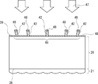
- FIG. 1 shows a cross-sectional view of a transmissive screen 20.
- the screen 20 includes a microlens array 21 and an aperture array 24.
- the aperture array 24 is disposed on the surface opposite to the surface on which the microlens array 21 is disposed.
- the microlens array 21 and the aperture array 24 are disposed on a transparent substrate 28 made of resin.
- the individual microlenses 22 included in the microlens array 21 cause diffusion 32 of the image light 31. Therefore, the screen 20 functions as an optical screen because the direction of the optical axis of the image light 31 is dispersed.
- the microlens 22 can be designed to have a desired diffusion angle in the diffusion 32. You may define as a full angle the position which becomes the half value of the center brightness
- the microlens 22 has a convex surface that projects outward from the screen 20, that is, downward in the drawing.
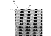
- the opening array 24 shown in FIG. 1 includes a light shielding part 25 and an opening part 26. Therefore, the image light 31 diffused as described above finally passes through the screen 20 via the opening 26.
- the light shielding portion 25 is preferably provided only in a portion other than the portion through which the image light 31 is transmitted.
- the inner diameter of the opening 26 shown in FIG. 1 is preferably equal to or larger than the diameter of the spread of the image light 31 on the cross section of the image light 31 in the opening 26.
- a head-up display with a screen 20 is designed as such. In this manner, the image light 31 reflected from the inner surface 29 of the light shielding unit 25 can be reduced.
- the inner surface 29 is a surface that the light shielding unit 25 has and is a surface that is located on the top surface side of the transparent substrate 28. That is, the surface opposite to the outer surface 27.
- FIG. 2 is an image obtained by photographing one of the examples of the aperture array 24. As shown in the photographed image, the openings 26 are arranged in a lattice pattern on the opening array 24. The opening 26 is surrounded by the light shielding portion 25.
- the light shielding part 25 is a metal film.
- the metal film is preferably a film formed by any of vapor deposition, sputtering and electroforming. The metal film is preferably a deposited film.
- the outer surface 27 of the metal film constituting the light shielding portion 25 has a mirror surface.
- the outer surface 27 is a surface far from the microlens array 21.
- the reflectance of light having a wavelength of 380 nm to 780 nm is preferably 80% or more, more preferably 83% or more, and further preferably 87% or more.
- the reflectance of the outer surface 27 shown in FIG. 1 is, for example, a metal film produced in the same manner as the light shielding portion 25 and having no opening, and light is reflected by a spectrophotometer. It is obtained from the value when the thickness is measured. In this measurement, the incident light is preferably incident on the outer surface 27 at an angle of 10 degrees with respect to the normal line of the outer surface 27.
- U-4100 made by Hitachi High-Tech Science may be used as the spectrophotometer.
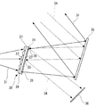
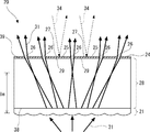
- FIG. 3 shows the optical system 30 of the head-up display.
- a head-up display includes a screen 20.
- the screen 20 constitutes a part of the optical system 30.
- the image light 31 represented by a solid line is projected onto the screen 20 from the microlens array 21 side.
- the image light 31 is generated by, for example, PGU (Picture Generation Unit).
- PGU Picture Generation Unit
- the image light 31 is guided to the screen 20 by the projection optical system.
- the image light 31 shown in FIG. 3 is diffused by the microlens array 21.
- the image light 31 passes through the screen 20.
- the image light 31 is emitted from the screen 20 as diffused light and is reflected by the concave mirror 35. Thereafter, the video light 31 is presented as a virtual image to an observer who views the head-up display.
- the screen 20 includes a microlens array 21.
- the diffusion angle and efficiency of the screen 20 can be easily controlled by the microlens array 21.
- the image presented by the video light 31 can be adjusted to an angle of view that is easy for an observer to visually recognize.
- a head-up display is mounted on a vehicle and the vehicle is placed outdoors.
- sunlight may enter the optical system 30 shown in FIG.
- external light 34 represented by a broken line is reflected by the concave mirror 35.
- the external light 34 may reach the screen 20 after reflection.
- the external light 34 entering from the opposite direction to the image light 31 is reflected by the screen 20. Specifically, the light is reflected by the microlens array 21 or the aperture array 24. At this time, since the optical axis of the video light 31 and the optical axis of the external light 34 are parallel, the external light 34 may be mixed with the video light 31.
- the image presented by the video light 31 is whitened. Therefore, the contrast of the image is lowered.
- a driver of a vehicle not only the visibility of the image is deteriorated, but also a dazzling part is visually recognized in the image.
- Such a problem is not limited to the case where the external light 34 is sunlight. The same problem occurs even when the head-up display is not mounted on the vehicle.
- the screen 20 is inclined so that the optical axis of the image light 31 emitted from the opening 26 and the optical axis of the external light 34 reflected by the light shielding unit 25 are not parallel. is there.
- the screen 20 is tilted so that the screen 20 is inclined with respect to the optical axis of the image light 31 projected on the screen 20 from the microlens array 21 side.
- the incoming external light 34 can escape in a direction different from the optical axis of the image light 31. Accordingly, since the external light 34 is not easily mixed with the video light 31, whitening of the image is suppressed.
- the head-up display of this embodiment further includes a light absorption unit 36.
- the light absorption unit 36 receives external light 34 reflected by the light shielding unit 25.
- the light absorption part 36 is subjected to black coating, anodizing, or the like.
- the light absorption unit 36 absorbs external light 34. For this reason, the external light 34 is suppressed from becoming stray light in the optical system 30.
- the contrast of an image can be increased even when a black matrix such as a black resist is used as an alternative to the light shielding portion 25.
- a black matrix such as a black resist
- the external light 34 shown in FIG. 3 is collected on the screen by the concave mirror 35, the energy of the external light 34 is efficiently absorbed by the black matrix. Therefore, the screen tends to overheat with the black matrix.
- the screen is made of a transparent substrate made of resin, there is a possibility that the screen may be deformed or ignited. For this reason, in a head-up display, an absorption type contrast improving means such as a black matrix is not suitable for the screen. Such a problem is not limited to the case where the external light 34 is sunlight. The same problem occurs even when the head-up display is not mounted on the vehicle.
- the external light 34 that has reached the screen 20 can be released to the light absorber 36.
- the screen 20 is provided with a light shielding portion 25 made of a metal film.
- the light shielding unit 25 reflects the external light 34 by regular reflection. For this reason, since the light shielding part 25 is hard to overheat, the screen 20 is also hard to overheat.
- the microlens array 21 shown in FIG. 1 can be formed as a sheet according to a known method.
- the mold used for forming the microlens array sheet may be formed by cutting.
- a mold may be formed by photolithography, and a mold may be formed based on the mold.
- the mold may be produced by laser ablation. Any mold can be used as long as it can withstand the molding of the microlens array sheet.
- a resin sheet such as injection molding, press molding, and molding by ultraviolet curing
- a sheet obtained by molding may be attached to the transparent substrate 28.
- self-alignment exposure it is preferable to use self-alignment exposure as a pattern forming method.
- the photoresist is exposed using the condensing function of the microlens array 21 itself shown in FIGS.
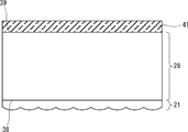
- FIG. 4 is a schematic diagram of resist application.
- the microlens array 21 is formed on one surface of the transparent substrate 28, that is, the bottom surface 38.
- a resist 41 is applied to the top surface 39 of the transparent substrate 28.
- the top surface 39 is a surface opposite to the bottom surface 38.
- the resist 41 is a negative resist.
- the resist 41 is preferably a photosensitive resin.
- spin coating, die coating, spray coating, roll coating, or the like can be used. Further, drying is performed to volatilize the solvent of the applied resist 41. For drying, a hot plate, an oven, a vacuum dryer, an infrared heater, or the like can be used. As a method of not applying and drying, a method of laminating a film resist can be taken.
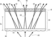
- FIG. 5 is a schematic diagram of resist exposure.
- Exposure light 44 is irradiated from the microlens array 21 side toward the transparent substrate 28.
- the exposure light 44 is preferably ultraviolet light.
- the exposure light 44 is collected by each microlens of the microlens array 21.
- the resist 41 is exposed with the exposure light 44.
- the aperture diameter may change according to the focal length and the diffusion angle of the microlens.
- the light source of the exposure light 44 is preferably a light source that can emit light having substantially the same projection angle and pupil diameter as the image light 31 shown in FIG.
- the light source of the exposure light 44 is preferably a light source having a small viewing angle.
- Performing self-alignment exposure as described above is suitable for transmitting exposure light in substantially the same optical path as the image light 31 as shown in FIG. That is, if the image light is irradiated onto the resist 41 shown in FIG. 4, it is suitable for exposing only a part of the resist 41 that is considered to transmit the image light. This portion of the resist 41 changes to an exposed resist 42 shown in FIG.
- FIG. 6 shows a process of forming the metal film 43.
- the resist 41 and the resist to be exposed 42 shown in FIG. 5 are developed.
- the exposed resist is exposed to the developer together with the transparent base plate 28.
- an alkali developer suitable for the material used for the resist 41 may be used.
- an immersion method, a rocking method, a paddle method, a spray method, or the like can be used. After development, it is washed with pure water and dried.
- a resist pattern 45 shown in FIG. 6 is formed.
- a metal film 48 is formed on the top surface 39 on which the resist pattern 45 is formed.
- the formation of the metal film 48 may be performed by any one of vapor deposition, sputtering, and electroforming, but is not limited thereto.
- the resist pattern 45 shown in FIG. 6 is removed from the transparent substrate 28. By removing the resist pattern 45, an opening array 24 made of the metal film 48 (FIG. 6) is formed as shown in FIG. An opening 26 as shown in FIG. 2 is formed at the portion where the exposed resist 42 is removed. Thus, the screen 20 can be manufactured.
- the transparent substrate 28 is preferably removed by lift-off.
- the lift-off it is preferable to bring the solvent into contact with the resist 42 to be exposed. Further, it is preferable to remove the resist pattern 45 by immersing the transparent substrate 28 together in the lift-off solution.
- the lift-off solution may be warmed to facilitate lift-off. In order to promote lift-off, the transparent substrate 28 may be vibrated.
- the exposed portion of the exposed resist 42 shown in FIG. 6 that is not covered with the metal film 48 is required.
- a vapor deposition method is suitable as a means for forming the metal film 48 shown in FIG.
- the metal particles go straight as the vapor flow 47. For this reason, the metal particles rarely wrap around the side surface of the exposed resist 42. Therefore, the side surface of the exposed resist 42 is not easily covered with the metal film 48.
- the aperture array shields light other than the portion through which the image light 31 passes. This is because the exposure light 44 shown in FIG. 5 passes through the site where the opening 26 through which the image light 31 shown in FIG. 7 passes should be formed by the self-alignment method. That is, the essential point of the resist pattern formation of the present embodiment is to provide the resist 42 to be exposed at the site where the opening 26 is to be formed by the self-alignment method.
- a head-up display can be manufactured by producing a screen by the self-alignment method and disposing the screen in the head-up display.
- the screen 20 is arranged so that the image light 31 is projected onto the screen 20 from the microlens array 21 side shown in FIG.
- the image light 31 is efficiently transmitted through the opening 26. This is because, by the self-alignment method, the opening 26 is accurately provided in advance at a position where the image light 31 should be transmitted.
- At least one of the exposure light 44 shown in FIG. 5 and the image light 31 shown in FIG. 7 may be adjusted.
- the image point distance Ex of the exposure light 44 shown in FIG. 5 and the image point distance Im of the video light 31 shown in FIG. 7 may be adjusted to be equal.
- the difference between these image point distances is preferably in the range of 10, 9, 8, 7, 6, 5, 4, 3, 2, and 1%.
- the inner diameter of the opening 26 shown in FIG. 7 can be made substantially equal to the diameter of the spread of the image light 31 on the cross section in the opening 26. While reducing the image light 31 reflected by the inner surface 29 of the light shielding part 25, the efficiency of reflection of the external light 34 by the light shielding part 25 can also be increased.
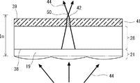
- the image point 50 is an image point of the exposure light 44 relating to the microlens included in the microlens array 21.
- the image point 50 is in front of the applied resist 41 with respect to the microlens.
- the image point 50 is in the transparent substrate 28 in the drawing, the image point 50 may be in the microlens array 21 in other embodiments.
- the exposed resist 42 shown in FIG. 6 becomes tapered as the distance from the microlens array 21 increases.
- the exposed resist 42 has a so-called reverse taper shape. This is because, as shown in FIG. 5, when the exposure light 44 reaches the resist to be exposed 42, the exposure light 44 has already passed the image point 50, and the exposure light 44 is in the process of diverging.
- the angle of the steam flow 47 with respect to the top surface 39 is not limited. This is because the side surface of the exposed resist 42 having a reverse taper shape is always shaded in any direction with respect to the vapor flow 47.
- the direction of the vapor flow 47 that collides with the top surface 39 shown in FIG. 6 is not inclined with respect to the normal direction of the top surface 39. Further, the direction of the vapor flow 47 may be inclined from 0 ° to 20 °. The range of such inclination is preferably 0 ° to 10 °, more preferably 0 ° to 5 °. The smaller the inclination, the more efficiently the metal film 46 can be made thicker.
- the positional relationship between the image point 50 shown in FIG. 5 and the applied resist 41 can be arbitrarily adjusted. Such positional relationship can be adjusted, for example, by the thickness of at least one of the transparent substrate 28 and the base portion 19 of the microlens array 21. However, when the sum of these thicknesses increases and the image point distance Ex of the image point 50 does not change, the distance from the main surface of the microlens array 21 to the resist 41 becomes relatively large. In the figure, the image point distance Ex of the image point 50 also takes into account that the exposure light 44 is refracted at the interface between the microlens array 21 and the transparent substrate 28. The image point distance Im of the image light 31 shown in FIG.
- each of the adjacent microlenses in the microlens array 21 has the same distance.
- the diffused exposure light 44 may overlap each other in the resist 41. In this case, most of the resist 41 is exposed. Accordingly, as shown in FIG. 2, the opening 26 surrounded by the light shielding portion 25 cannot be formed. For this reason, the aperture array 24 shown in FIG. 3 cannot reflect the external light 34 efficiently.
- FIG. 8 shows another aspect of resist exposure.
- the exposure light 44 diffused by each microlens is partially omitted for convenience of explanation.
- the distance from the main surface of the microlens array 21 to the resist 41 becomes relatively small.
- the image point of the exposure light 44 relating to the microlens of the microlens array 21 is farther than the resist 41 with respect to the microlens.
- the image point distance Ex of the image point 50 is that the exposure light 44 is refracted by the transparent substrate 28 and the resist 41.
- the exposed resist 42 shown in FIG. 8 becomes tapered as the distance from the microlens array 21 increases.
- the exposed resist 42 has a so-called forward tapered shape. This is because, as shown in the figure, when the exposure light 44 reaches the resist to be exposed 42, the exposure light 44 has not yet passed the image point, and the exposure light 44 is in the process of convergence.
- the exposed portion of the side surface of the resist 42 to be exposed is not covered with the metal film 48.
- the magnitude of the inclination in the direction of the vapor flow 51 impinging on the top surface 39 is indicated by the vapor deposition angle Va with reference to the normal direction of the top surface 39.
- the vapor deposition angle Va exceeds 60 °, the portion of the top surface 39 that is the shadow of the resist to be exposed 42 may become large. For this reason, a sufficient amount of metal to form the light shielding portion cannot be sent to the shaded portion.
- the exposed resist 42 has a substantially cylindrical shape with a diameter of 10 ⁇ m.
- the pitch of the openings in the opening array formed on the exposed resist 42 is 20 ⁇ m.
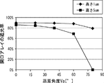
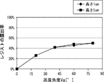
- the height of the exposed resist 42 is 1 ⁇ m or 5 ⁇ m. Compared with the height of 1 ⁇ m, the shadowed portion of the exposed resist 42 becomes larger in the case of the height of 5 ⁇ m. For this reason, when the height is 5 ⁇ m, the light blocking ratio is smaller than when the height is 1 ⁇ m. In the case where the height of the resist to be exposed 42 is 5 ⁇ m, the light shielding rate is drastically lowered when the deposition angle Va is larger than 60 °.
- the resist exposure rate represents an exposure rate based on the area of the side surface of the exposed resist 42 shown in FIG. There is almost no difference in the exposure rate when the height of the exposed resist 42 is 1 ⁇ m and when it is 5 ⁇ m.
- the deposition angle Va larger than 0 °, the side surface of the resist 42 to be exposed can be exposed.
- the deposition angle Va shown in FIG. The thickness of the deposited film, The size of the portion to be exposed on the side surface of the exposed resist 42; The size of the portion of the top surface 39 that is not deposited behind the exposed resist 42; Can be determined in a complementary manner.
- the deposition angle Va shown in FIG. 9 can be in the range of 20 ° to 60 °.
- the vapor deposition angle Va is preferably 45 °. With this deposition angle Va, lift-off can be efficiently performed by suppressing metal deposition on the side surface of the resist 42 to be exposed. Furthermore, it is possible to efficiently deposit metal on a portion of the top surface 39 where the light shielding portion is to be formed.
- the present invention is not limited to the above-described embodiment, and can be appropriately changed without departing from the spirit of the present invention.
- the transparent substrate 28 and the microlens array 21 shown in FIG. 1 may be molded as a seamless integral member.
- a microlens array sheet including the transparent substrate 28 and the microlens array 21 shown in FIG. 4 was formed.
- the microlens array 21 was formed on a transparent substrate 28 made of polycarbonate film using an ultraviolet curable resin.
- the thickness of the polycarbonate film was 100 ⁇ m.
- An acrylic resin was used as the ultraviolet curable resin.
- the irradiation amount of ultraviolet rays was 500 mJ / cm 2 .
- a resist 41 was applied to the back side of the microlens array sheet, that is, the top surface 39. Application was performed by a spin coating method. The rotational speed of the microlens array sheet, which is a workpiece, was adjusted so that the film thickness of the resist 41 was 5 ⁇ m.
- PMER N-CA3000 which is a negative type photoresist made by Tokyo Ohka, was used. The resist 41 was dried in an oven at 70 ° C. for 20 minutes.
- the microlens array sheet was placed on the stage of the UV exposure apparatus. At this time, the microlens array 21 shown in FIG. Ultraviolet rays were irradiated from the microlens array 21 side. The exposure amount was 500 mJ / cm 2 . After the exposure, the microlens array sheet was subjected to a PEB (post exposure bake) treatment at 70 ° C. for 20 minutes in an oven.
- PEB post exposure bake
- the microlens array sheet was immersed in an organic alkali developer (TMAH 2.38%). The microlens array sheet was rocked for 3 minutes. The microlens array sheet taken out from the developer was washed with pure water and further dried.
- TMAH organic alkali developer
- the metal film 48 shown in FIG. 6 was formed with a vacuum deposition apparatus. However, the vapor deposition angle was 45 °. The weight of the vapor deposition source was 10.4 g. The thickness of the deposited film was about 200 nm.
- the lift-off was performed by immersing the deposited microlens array sheet in NMP (n-methyl-2-pyrrolidone). The microlens array sheet was rocked for 180 seconds. As a result, the exposed resist 42 was dissolved to form the opening array 24 shown in FIG. This obtained the screen of the Example. The screen taken out from NMP was washed with pure water and then naturally dried.
- a screen of a comparative example was made up to the formation of a microlens array with an ultraviolet curable resin in the examples.
- the reflection characteristics of the back side of the microphone lens array sheet, that is, the top surface 39 side shown in FIG. 7 were evaluated.
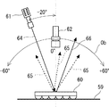
- FIG. 12 shows a schematic diagram of an apparatus for evaluating reflection characteristics.
- This apparatus is a goniometer for measuring the intensity distribution of reflected light according to the reflection angle when the test screen 60 is irradiated with external light 64.
- the test screen 60 was placed on the black sheet 59 with the microlens array side down.
- LED pseudo-parallel light having a spread angle of 5 ° or less was used as the external light 64 shown in FIG. 12.
- a light source 61 that emits such parallel light is disposed.
- a part of the external light 64 is diffusely reflected by the test screen 60 and becomes diffusely reflected light 65.
- Part of the external light 64 is specularly reflected by the test screen 60 and becomes specularly reflected light 66.
- the regular reflection light 66 is inclined + 20 °.
- the reflection angle was changed by changing the observation angle Ob of the surface luminance meter 62 from ⁇ 60 ° to + 60 °.
- the observation angle Ob is set to 0 °.
- the mounting angle of the test screen 60 when the test screen 60 is installed in the head-up display is assumed to be 20 °.
- the optical axis of the light source 61 and the optical axis of the surface luminance meter 62 when the observation angle Ob is 0 ° are shifted by ⁇ 20 °.
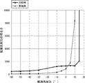
- FIG. 13 is a graph showing the correlation between the brightness of the diffuse reflected light and the observation angle.
- the unit of brightness of the diffuse reflected light is cd / m 2 .
- the inclination angle when attaching the screen to the head-up display is 20 °. Therefore, strong specular reflection light is prevented from entering the observer's eyes.
Landscapes
- Physics & Mathematics (AREA)
- General Physics & Mathematics (AREA)
- Optics & Photonics (AREA)
- Optical Elements Other Than Lenses (AREA)
- Overhead Projectors And Projection Screens (AREA)
- Devices For Indicating Variable Information By Combining Individual Elements (AREA)
Abstract
Description
前記マイクロレンズアレイの配置された面の反対側の面に配置された開口アレイをさらに備え、
前記開口アレイの遮光部は金属膜である、
スクリーン。
[2] 前記金属膜は蒸着膜である、
[1]に記載のスクリーン。
[3] 前記金属膜の外表面は鏡面を有する、
[1]又は[2]に記載のスクリーン。
[4] 前記金属膜の外表面は波長380nmから780nmの光の反射率が80%以上である、
[1]~[3]のいずれかに記載のスクリーン。
[5] [1]~[4]のいずれかに記載のスクリーンを備えるヘッドアップディスプレイであって、
前記マイクロレンズアレイ側から前記スクリーンに映像光が投射され、
前記開口アレイの開口部の内径は、前記開口部における断面上の映像光の拡がりの径と等しいか、又はこれより大きい、
ヘッドアップディスプレイ。
[6] [1]~[4]のいずれかに記載のスクリーンを備えるヘッドアップディスプレイであって、
前記マイクロレンズアレイ側から前記スクリーンに投射される映像光の光軸に対して前記スクリーンが斜めになるように前記スクリーンが傾けてあり、
前記遮光部で反射した外光を吸収する吸光部をさらに備える、
ヘッドアップディスプレイ。
[7] マイクロレンズアレイと前記マイクロレンズアレイの反対側に配置された開口アレイとを備える透過型のスクリーンの製造方法であって、
片面にマイクロレンズアレイの形成された透明基材上に開口アレイを形成する際、
前記透明基材のマイクロレンズアレイの配置された面の反対側の面にネガティブレジストを塗布し、
前記マイクロレンズアレイ側から前記透明基材に向かって露光光を照射し、
前記露光光で前記ネガティブレジストを露光し、さらに現像することでレジストパターンを形成し、
前記レジストパターンを形成した前記透明基材の面上に金属膜を形成し、
前記レジストパターンを除去することで前記金属膜からなる開口アレイを形成する、
スクリーンの製造方法。
[8] 前記マイクロレンズアレイの有するマイクロレンズに関する前記露光光の像点は前記マイクロレンズに対して、前記塗布されたネガティブレジストよりも手前にあり、
前記金属膜は蒸着により形成し、
前記レジストパターンはリフトオフにより除去する、
[7]に記載のスクリーンの製造方法。
[9] 前記蒸着において、前記透明基材の面に衝突する蒸気流の方向が、前記透明基材の面の法線方向を基準として傾斜していない、又は0°から20°傾斜している、
[8]に記載のスクリーンの製造方法。
[10] 前記マイクロレンズアレイの有するマイクロレンズに関する前記露光光の像点は前記マイクロレンズに対して、前記塗布されたネガティブレジストよりも遠くにあり、
前記金属膜は蒸着により形成し、
前記レジストパターンはリフトオフにより除去し、
前記蒸着において、前記透明基材の面に衝突する蒸気流の方向が、前記透明基材の面の法線方向を基準として20°から60°傾斜している、
[7]に記載のスクリーンの製造方法。
[11] [7]~[10]のいずれかに記載の方法でスクリーンを作製し、
前記マイクロレンズアレイ側から前記スクリーンに映像光が投射されるように、前記スクリーンを配置するヘッドアップディスプレイの製造方法であって、
前記マイクロレンズアレイの有するマイクロレンズに関する前記露光光の像点距離と、前記映像光の像点距離とが等しくなるように、前記露光光及び前記映像光の少なくともいずれか一方を調整する、
ヘッドアップディスプレイの製造方法。
一方、開口アレイの形成では以下に留意する必要がある。すなわち図3に示すように開口アレイ24は外光34を遮るが、映像光31を遮らない。したがってマイクロレンズアレイ21におけるマイクロレンズ22の配置に基づき、透明基材28上に正確に開口アレイのパターンを形成する必要がある。
蒸着膜の厚みと、
被露光レジスト42の側面において露出させたい部分の大きさと、
被露光レジスト42の陰となって蒸着されない頂面39の部分の大きさと、
を相補的に加味して決定することができる。
Claims (11)
- マイクロレンズアレイを備える透過型のスクリーンであって、
前記マイクロレンズアレイの配置された面の反対側の面に配置された開口アレイをさらに備え、
前記開口アレイの遮光部は金属膜である、
スクリーン。 - 前記金属膜は蒸着膜である、
請求項1に記載のスクリーン。 - 前記金属膜の外表面は鏡面を有する、
請求項1又は2に記載のスクリーン。 - 前記金属膜の外表面は波長380nmから780nmの光の反射率が80%以上である、
請求項1~3のいずれかに記載のスクリーン。 - 請求項1~4のいずれかに記載のスクリーンを備えるヘッドアップディスプレイであって、
前記マイクロレンズアレイ側から前記スクリーンに映像光が投射され、
前記開口アレイの開口部の内径は、前記開口部における断面上の映像光の拡がりの径と等しいか、又はこれより大きい、
ヘッドアップディスプレイ。 - 請求項1~4のいずれかに記載のスクリーンを備えるヘッドアップディスプレイであって、
前記マイクロレンズアレイ側から前記スクリーンに投射される映像光の光軸に対して前記スクリーンが斜めになるように前記スクリーンが傾けてあり、
前記遮光部で反射した外光を吸収する吸光部をさらに備える、
ヘッドアップディスプレイ。 - マイクロレンズアレイと前記マイクロレンズアレイの反対側に配置された開口アレイとを備える透過型のスクリーンの製造方法であって、
片面にマイクロレンズアレイの形成された透明基材上に開口アレイを形成する際、
前記透明基材のマイクロレンズアレイの配置された面の反対側の面にネガティブレジストを塗布し、
前記マイクロレンズアレイ側から前記透明基材に向かって露光光を照射し、
前記露光光で前記ネガティブレジストを露光し、さらに現像することでレジストパターンを形成し、
前記レジストパターンを形成した前記透明基材の面上に金属膜を形成し、
前記レジストパターンを除去することで前記金属膜からなる開口アレイを形成する、
スクリーンの製造方法。 - 前記マイクロレンズアレイの有するマイクロレンズに関する前記露光光の像点は前記マイクロレンズに対して、前記塗布されたネガティブレジストよりも手前にあり、
前記金属膜は蒸着により形成し、
前記レジストパターンはリフトオフにより除去する、
請求項7に記載のスクリーンの製造方法。 - 前記蒸着において、前記透明基材の面に衝突する蒸気流の方向が、前記透明基材の面の法線方向を基準として傾斜していない、又は0°から20°傾斜している、
請求項8に記載のスクリーンの製造方法。 - 前記マイクロレンズアレイの有するマイクロレンズに関する前記露光光の像点は前記マイクロレンズに対して、前記塗布されたネガティブレジストよりも遠くにあり、
前記金属膜は蒸着により形成し、
前記レジストパターンはリフトオフにより除去し、
前記蒸着において、前記透明基材の面に衝突する蒸気流の方向が、前記透明基材の面の法線方向を基準として20°から60°傾斜している、
請求項7に記載のスクリーンの製造方法。 - 請求項7~10のいずれかに記載の方法でスクリーンを作製し、
前記マイクロレンズアレイ側から前記スクリーンに映像光が投射されるように、前記スクリーンを配置するヘッドアップディスプレイの製造方法であって、
前記マイクロレンズアレイの有するマイクロレンズに関する前記露光光の像点距離と、前記映像光の像点距離とが等しくなるように、前記露光光及び前記映像光の少なくともいずれか一方を調整する、
ヘッドアップディスプレイの製造方法。
Priority Applications (5)
| Application Number | Priority Date | Filing Date | Title |
|---|---|---|---|
| CN201780014969.6A CN108700797B (zh) | 2016-01-12 | 2017-01-11 | 平视显示器及其制造方法 |
| KR1020187021403A KR102164725B1 (ko) | 2016-01-12 | 2017-01-11 | 디스플레이용 스크린 |
| JP2017561121A JPWO2017122651A1 (ja) | 2016-01-12 | 2017-01-11 | ディスプレイ用スクリーン |
| US16/069,344 US10901122B2 (en) | 2016-01-12 | 2017-01-11 | Screen for display |
| EP17738405.4A EP3404484A4 (en) | 2016-01-12 | 2017-01-11 | SCREEN FOR DISPLAY |
Applications Claiming Priority (2)
| Application Number | Priority Date | Filing Date | Title |
|---|---|---|---|
| JP2016-003410 | 2016-01-12 | ||
| JP2016003410 | 2016-01-12 |
Publications (1)
| Publication Number | Publication Date |
|---|---|
| WO2017122651A1 true WO2017122651A1 (ja) | 2017-07-20 |
Family
ID=59310980
Family Applications (1)
| Application Number | Title | Priority Date | Filing Date |
|---|---|---|---|
| PCT/JP2017/000551 WO2017122651A1 (ja) | 2016-01-12 | 2017-01-11 | ディスプレイ用スクリーン |
Country Status (6)
| Country | Link |
|---|---|
| US (1) | US10901122B2 (ja) |
| EP (1) | EP3404484A4 (ja) |
| JP (1) | JPWO2017122651A1 (ja) |
| KR (1) | KR102164725B1 (ja) |
| CN (1) | CN108700797B (ja) |
| WO (1) | WO2017122651A1 (ja) |
Cited By (4)
| Publication number | Priority date | Publication date | Assignee | Title |
|---|---|---|---|---|
| WO2019142431A1 (ja) * | 2018-01-18 | 2019-07-25 | 株式会社Jvcケンウッド | マイクロレンズアレイユニット及び表示装置 |
| JP2019164230A (ja) * | 2018-03-19 | 2019-09-26 | 株式会社リコー | 画像投写装置及び移動体 |
| WO2020039847A1 (en) * | 2018-08-21 | 2020-02-27 | Ricoh Company, Ltd. | Image projection apparatus, diffusion screen, and mobile object |
| KR20200026301A (ko) * | 2017-08-22 | 2020-03-10 | 콘티넨탈 오토모티브 게엠베하 | 헤드업 디스플레이 |
Families Citing this family (13)
| Publication number | Priority date | Publication date | Assignee | Title |
|---|---|---|---|---|
| DE102016211511A1 (de) * | 2016-06-27 | 2017-12-28 | Carl Zeiss Smt Gmbh | Beleuchtungseinheit für die Mikrolithographie |
| US11067884B2 (en) | 2018-12-26 | 2021-07-20 | Apple Inc. | Through-display optical transmission, reception, or sensing through micro-optic elements |
| US10838556B2 (en) | 2019-04-05 | 2020-11-17 | Apple Inc. | Sensing system for detection of light incident to a light emitting layer of an electronic device display |
| US11527582B1 (en) | 2019-09-24 | 2022-12-13 | Apple Inc. | Display stack with integrated photodetectors |
| US11611058B2 (en) | 2019-09-24 | 2023-03-21 | Apple Inc. | Devices and systems for under display image sensor |
| US11592873B2 (en) | 2020-02-14 | 2023-02-28 | Apple Inc. | Display stack topologies for under-display optical transceivers |
| US11295664B2 (en) | 2020-03-11 | 2022-04-05 | Apple Inc. | Display-synchronized optical emitters and transceivers |
| CN115769110A (zh) * | 2020-05-15 | 2023-03-07 | 三星电子株式会社 | 反射结构、包括该反射结构的反射结构阵列以及浮动图像显示装置 |
| US11327237B2 (en) | 2020-06-18 | 2022-05-10 | Apple Inc. | Display-adjacent optical emission or reception using optical fibers |
| US11487859B2 (en) | 2020-07-31 | 2022-11-01 | Apple Inc. | Behind display polarized optical transceiver |
| US11839133B2 (en) | 2021-03-12 | 2023-12-05 | Apple Inc. | Organic photodetectors for in-cell optical sensing |
| US12124002B2 (en) | 2021-09-03 | 2024-10-22 | Apple Inc. | Beam deflector metasurface |
| GB2624439A (en) * | 2022-11-18 | 2024-05-22 | Envisics Ltd | Manufacture of reflection suppression device |
Citations (8)
| Publication number | Priority date | Publication date | Assignee | Title |
|---|---|---|---|---|
| US6829086B1 (en) * | 1999-04-29 | 2004-12-07 | Synelec Telecom Multimedia | Projection screen |
| JP2007199212A (ja) * | 2006-01-24 | 2007-08-09 | Seiko Epson Corp | マイクロレンズ基板、透過型スクリーンおよびリア型プロジェクタ |
| JP2007240713A (ja) * | 2006-03-07 | 2007-09-20 | Toppan Printing Co Ltd | レンズシート及び透過型プロジェクションスクリーン |
| JP2009500662A (ja) * | 2005-06-29 | 2009-01-08 | リフレキサイト・コーポレーション | コリメーティングマイクロレンズアレイ |
| JP2012208440A (ja) | 2011-03-30 | 2012-10-25 | Nippon Seiki Co Ltd | ヘッドアップディスプレイ装置 |
| JP2014149405A (ja) * | 2013-01-31 | 2014-08-21 | Nippon Seiki Co Ltd | ヘッドアップディスプレイ装置 |
| JP2016003410A (ja) | 2014-06-16 | 2016-01-12 | 株式会社シーエフ | 羽毛の光触媒加工法及び装置 |
| JP2016122059A (ja) * | 2014-12-24 | 2016-07-07 | 日本精機株式会社 | ヘッドアップディスプレイ |
Family Cites Families (10)
| Publication number | Priority date | Publication date | Assignee | Title |
|---|---|---|---|---|
| JPH1039769A (ja) | 1996-07-19 | 1998-02-13 | Toray Ind Inc | マイクロレンズアレイシート |
| JPH10241434A (ja) | 1997-02-27 | 1998-09-11 | Toray Ind Inc | 光線指向性化シートおよびそれを用いた指向性面状光源 |
| JPH11344602A (ja) * | 1998-03-30 | 1999-12-14 | Seiko Epson Corp | ブラックマトリクス付マイクロレンズ基板の製造方法、液晶パネル用対向基板、液晶パネルおよび投射型表示装置 |
| JP2001201611A (ja) * | 2000-01-21 | 2001-07-27 | Hitachi Ltd | 光学的機能性シート及びこれを用いた面状光源並びに画像表示装置 |
| JP3731592B2 (ja) * | 2003-09-08 | 2006-01-05 | セイコーエプソン株式会社 | 透過型スクリーン用部材、透過型スクリーンおよびリア型プロジェクタ |
| JP2006330631A (ja) * | 2005-05-30 | 2006-12-07 | Miraial Kk | 背面投射型スクリーン |
| JP2007212887A (ja) * | 2006-02-10 | 2007-08-23 | Miraial Kk | 異方性光吸収シート、異方性光吸収シートの製造方法、異方性光吸収シート用金型の製造方法、及び、画像投射装置用スクリーン |
| JP4896553B2 (ja) * | 2006-03-29 | 2012-03-14 | 藤森工業株式会社 | マイクロレンズアレイシートの製造方法 |
| WO2012124524A1 (ja) * | 2011-03-11 | 2012-09-20 | シャープ株式会社 | 蒸着粒子射出装置および蒸着装置 |
| US20140198368A1 (en) * | 2013-01-17 | 2014-07-17 | Koc University | High Gain Display Screen with Rotated Microlens Array |
-
2017
- 2017-01-11 EP EP17738405.4A patent/EP3404484A4/en not_active Withdrawn
- 2017-01-11 KR KR1020187021403A patent/KR102164725B1/ko active IP Right Grant
- 2017-01-11 CN CN201780014969.6A patent/CN108700797B/zh not_active Expired - Fee Related
- 2017-01-11 JP JP2017561121A patent/JPWO2017122651A1/ja active Pending
- 2017-01-11 WO PCT/JP2017/000551 patent/WO2017122651A1/ja active Application Filing
- 2017-01-11 US US16/069,344 patent/US10901122B2/en active Active
Patent Citations (8)
| Publication number | Priority date | Publication date | Assignee | Title |
|---|---|---|---|---|
| US6829086B1 (en) * | 1999-04-29 | 2004-12-07 | Synelec Telecom Multimedia | Projection screen |
| JP2009500662A (ja) * | 2005-06-29 | 2009-01-08 | リフレキサイト・コーポレーション | コリメーティングマイクロレンズアレイ |
| JP2007199212A (ja) * | 2006-01-24 | 2007-08-09 | Seiko Epson Corp | マイクロレンズ基板、透過型スクリーンおよびリア型プロジェクタ |
| JP2007240713A (ja) * | 2006-03-07 | 2007-09-20 | Toppan Printing Co Ltd | レンズシート及び透過型プロジェクションスクリーン |
| JP2012208440A (ja) | 2011-03-30 | 2012-10-25 | Nippon Seiki Co Ltd | ヘッドアップディスプレイ装置 |
| JP2014149405A (ja) * | 2013-01-31 | 2014-08-21 | Nippon Seiki Co Ltd | ヘッドアップディスプレイ装置 |
| JP2016003410A (ja) | 2014-06-16 | 2016-01-12 | 株式会社シーエフ | 羽毛の光触媒加工法及び装置 |
| JP2016122059A (ja) * | 2014-12-24 | 2016-07-07 | 日本精機株式会社 | ヘッドアップディスプレイ |
Non-Patent Citations (1)
| Title |
|---|
| See also references of EP3404484A4 |
Cited By (6)
| Publication number | Priority date | Publication date | Assignee | Title |
|---|---|---|---|---|
| KR20200026301A (ko) * | 2017-08-22 | 2020-03-10 | 콘티넨탈 오토모티브 게엠베하 | 헤드업 디스플레이 |
| KR102468923B1 (ko) * | 2017-08-22 | 2022-11-18 | 콘티넨탈 오토모티브 게엠베하 | 헤드업 디스플레이 |
| US11531198B2 (en) | 2017-08-22 | 2022-12-20 | Continental Automotive Gmbh | Head-up display |
| WO2019142431A1 (ja) * | 2018-01-18 | 2019-07-25 | 株式会社Jvcケンウッド | マイクロレンズアレイユニット及び表示装置 |
| JP2019164230A (ja) * | 2018-03-19 | 2019-09-26 | 株式会社リコー | 画像投写装置及び移動体 |
| WO2020039847A1 (en) * | 2018-08-21 | 2020-02-27 | Ricoh Company, Ltd. | Image projection apparatus, diffusion screen, and mobile object |
Also Published As
| Publication number | Publication date |
|---|---|
| US20190018170A1 (en) | 2019-01-17 |
| EP3404484A1 (en) | 2018-11-21 |
| EP3404484A4 (en) | 2019-09-11 |
| JPWO2017122651A1 (ja) | 2018-12-27 |
| US10901122B2 (en) | 2021-01-26 |
| KR102164725B1 (ko) | 2020-10-13 |
| CN108700797B (zh) | 2020-12-08 |
| KR20180095936A (ko) | 2018-08-28 |
| CN108700797A (zh) | 2018-10-23 |
Similar Documents
| Publication | Publication Date | Title |
|---|---|---|
| WO2017122651A1 (ja) | ディスプレイ用スクリーン | |
| JP7142701B2 (ja) | 自動車投光器用の投射装置、及び投射装置を製造するための方法 | |
| JP4224547B2 (ja) | 像スクリーンおよびその上への光吸収層の形成方法 | |
| CN111077722B (zh) | 投影屏幕及其加工方法 | |
| KR100538298B1 (ko) | 차광성층을 갖춘 렌티큘라 렌즈시트 및 그 제조방법 | |
| US7787184B2 (en) | Member having antireflection structure | |
| WO2020042563A1 (zh) | 投影屏幕及其制造方法 | |
| JP2006065266A (ja) | 反射スクリーン、反射投影システム、及び、反射スクリーンの製造方法 | |
| JP4629473B2 (ja) | 固体撮像素子の製造方法 | |
| JP2001074918A (ja) | 光拡散体およびその製造方法 | |
| WO2006053176A2 (en) | Front-projection screen with subsurface diffusion targets | |
| TWI308987B (en) | Projecting device | |
| JPH10260638A (ja) | レンチキュラースクリーン及びその製造方法 | |
| JP2019020483A (ja) | ディスプレイ用スクリーン、及びその製造方法 | |
| JP2019020484A (ja) | ディスプレイ用スクリーン、及びその製造方法 | |
| JP2007047216A (ja) | レンズ基板の製造方法、レンズ基板、透過型スクリーンおよびリア型プロジェクタ | |
| JP2019144470A (ja) | ヘッドアップディスプレイ装置 | |
| TWI228745B (en) | Projection optics apparatus and thereof display device and thereof manufacturing method | |
| JP2004302005A (ja) | 透過型スクリーン | |
| JP2006323113A (ja) | レンズ基板、透過型スクリーンおよびリア型プロジェクタ | |
| KR100662911B1 (ko) | 렌티큘라 렌즈시트와 그 제조방법 | |
| JP2004191429A (ja) | 透過型スクリーン、その製造方法、及び背面投影型プロジェクション装置 | |
| JP2006308991A (ja) | 投写型表示装置 | |
| TWI232993B (en) | Projection optics apparatus and thereof display device and thereof manufacturing method | |
| JP2006308990A (ja) | 投写型表示装置及び照明光学系 |
Legal Events
| Date | Code | Title | Description |
|---|---|---|---|
| 121 | Ep: the epo has been informed by wipo that ep was designated in this application |
Ref document number: 17738405 Country of ref document: EP Kind code of ref document: A1 |
|
| ENP | Entry into the national phase |
Ref document number: 2017561121 Country of ref document: JP Kind code of ref document: A |
|
| NENP | Non-entry into the national phase |
Ref country code: DE |
|
| ENP | Entry into the national phase |
Ref document number: 20187021403 Country of ref document: KR Kind code of ref document: A |
|
| WWE | Wipo information: entry into national phase |
Ref document number: 1020187021403 Country of ref document: KR |
|
| WWE | Wipo information: entry into national phase |
Ref document number: 2017738405 Country of ref document: EP |
|
| ENP | Entry into the national phase |
Ref document number: 2017738405 Country of ref document: EP Effective date: 20180813 |