WO2017122347A1 - 制御システム - Google Patents
制御システム Download PDFInfo
- Publication number
- WO2017122347A1 WO2017122347A1 PCT/JP2016/051134 JP2016051134W WO2017122347A1 WO 2017122347 A1 WO2017122347 A1 WO 2017122347A1 JP 2016051134 W JP2016051134 W JP 2016051134W WO 2017122347 A1 WO2017122347 A1 WO 2017122347A1
- Authority
- WO
- WIPO (PCT)
- Prior art keywords
- data signal
- control circuit
- nth
- communication
- signal
- Prior art date
- Legal status (The legal status is an assumption and is not a legal conclusion. Google has not performed a legal analysis and makes no representation as to the accuracy of the status listed.)
- Ceased
Links
Images





Classifications
-
- H—ELECTRICITY
- H02—GENERATION; CONVERSION OR DISTRIBUTION OF ELECTRIC POWER
- H02M—APPARATUS FOR CONVERSION BETWEEN AC AND AC, BETWEEN AC AND DC, OR BETWEEN DC AND DC, AND FOR USE WITH MAINS OR SIMILAR POWER SUPPLY SYSTEMS; CONVERSION OF DC OR AC INPUT POWER INTO SURGE OUTPUT POWER; CONTROL OR REGULATION THEREOF
- H02M7/00—Conversion of AC power input into DC power output; Conversion of DC power input into AC power output
- H02M7/42—Conversion of DC power input into AC power output without possibility of reversal
- H02M7/44—Conversion of DC power input into AC power output without possibility of reversal by static converters
- H02M7/48—Conversion of DC power input into AC power output without possibility of reversal by static converters using discharge tubes with control electrode or semiconductor devices with control electrode
- H02M7/493—Conversion of DC power input into AC power output without possibility of reversal by static converters using discharge tubes with control electrode or semiconductor devices with control electrode the static converters being arranged for operation in parallel
-
- H—ELECTRICITY
- H04—ELECTRIC COMMUNICATION TECHNIQUE
- H04L—TRANSMISSION OF DIGITAL INFORMATION, e.g. TELEGRAPHIC COMMUNICATION
- H04L12/00—Data switching networks
- H04L12/28—Data switching networks characterised by path configuration, e.g. LAN [Local Area Networks] or WAN [Wide Area Networks]
-
- H—ELECTRICITY
- H04—ELECTRIC COMMUNICATION TECHNIQUE
- H04L—TRANSMISSION OF DIGITAL INFORMATION, e.g. TELEGRAPHIC COMMUNICATION
- H04L12/00—Data switching networks
- H04L12/28—Data switching networks characterised by path configuration, e.g. LAN [Local Area Networks] or WAN [Wide Area Networks]
- H04L12/42—Loop networks
- H04L12/437—Ring fault isolation or reconfiguration
Definitions
- the present invention relates to a control system, and more particularly to a control system provided with a plurality of control circuits for controlling a plurality of electric devices.
- Patent Document 1 discloses a power conversion system including m power conversion devices connected in parallel to a load and a communication line connected to the m power conversion devices. ing. m is an integer of 2 or more.
- Each power converter includes an inverter that converts DC power into AC power and supplies the load, a current sensor that detects a load current value, and another load current value detected by the current sensor via a communication line ( m-1) Transmit to each of the power converters and receive (m-1) load current values transmitted from the other (m-1) power converters via the communication line.
- the shared current and the cross current of the corresponding power converter are obtained.
- An arithmetic circuit and a control circuit that controls the inverter so that a shared current is supplied from the corresponding power converter to the load and cross current is eliminated.
- Patent Document 2 describes a combination of each data bit signal constituting each data signal to be transmitted and each exclusive OR of the modulation signal and the modulation signal as an upper bit signal.
- a serial signal transmission method for transmitting a serial signal using a combination of a data bit signal and an exclusive OR of the inverted signal of the modulated signal and the inverted signal of the modulated signal as a lower bit signal is disclosed.
- Patent Document 2 when the sum of the data bit signal corresponding to the upper bit signal and the lower bit signal of the serial signal is not a predetermined logical value on the receiving device side, the data bit signal is determined to be abnormal, and its use is Stopped.
- each power conversion device receives the load current value from the other (m ⁇ 1) power conversion devices and obtains the shared current and the cross current. Therefore, the amount of data communication increases and the communication speed increases. There was a problem of being slow.
- Patent Document 2 since the use of the data bit signal determined to be abnormal is stopped, it is necessary to stop the control of the control target when an abnormality occurs in the data bit signal.
- a main object of the present invention is to provide a control system capable of controlling a plurality of electrical devices even when a data signal communication is small, a communication speed is high, and an abnormality occurs in data signal communication. is there.
- a control system includes first to Nth control circuits for controlling first to Nth electrical devices, respectively, and first to Nth communication cables each including first and second communication lines. It is equipped with.
- N is an integer of 2 or more.
- the first to (N ⁇ 1) th control circuits are connected to the second to Nth control circuits in the subsequent stage via the first to (N ⁇ 1) th communication cables, respectively. It is connected to the first control circuit in the subsequent stage via N communication cables.
- the first control circuit generates a first data signal for controlling the first to Nth electric devices, controls the first electric device based on the first data signal, and controls the first data
- the signal is transmitted to the second control circuit at the subsequent stage via the first communication line of the first communication cable, and the first data signal is transmitted to the second control circuit at the preceding stage via the second communication line of the Nth communication cable. Transmit to the Nth control circuit.
- n is an integer greater than or equal to 2 and less than or equal to N
- the control circuit in the previous stage of the nth control circuit is the (n ⁇ 1) th control circuit
- the control circuit in the subsequent stage of the nth control circuit is the (n + 1) th control circuit.
- a first control circuit is an integer greater than or equal to 2 and less than or equal to N
- the nth control circuit controls the nth electrical device based on the first data signal, and generates an nth data signal indicating a control result of the nth electrical device.
- the nth control circuit receives the nth data signal and the data signal from the previous control circuit when the data signal communication with each of the previous control circuit and the subsequent control circuit is normally performed.
- the nth communication signal is transmitted to the subsequent control circuit via the first communication line of the nth communication cable, and the nth data signal and the data signal from the subsequent control circuit are transmitted to the (n ⁇ 1) th communication cable. 2 is transmitted to the control circuit in the previous stage via the two communication lines.
- the nth control circuit stops the communication of the data signal with the preceding control circuit, and the nth data signal and the succeeding control circuit.
- the data signal from the control circuit is transmitted to the subsequent control circuit via the first communication line of the nth communication cable.
- the nth control circuit stops the communication of the data signal with the subsequent control circuit and the nth data signal and the previous control circuit.
- the data signal from the control circuit is transmitted to the control circuit in the previous stage via the second communication line of the (n ⁇ 1) th communication cable.
- the first to Nth control circuits are connected in a ring shape with the first to Nth communication cables, the first control circuit serves as a master, and each of the second to Nth control circuits. Since this is a slave, it is possible to reduce the amount of data communication and increase the communication speed.
- the first to N-th control circuits and the first communication lines of the first to N-th communication cables are used.
- An annular first communication path is formed, and an annular second communication path is formed by the first to Nth control circuits and the second communication lines of the first to Nth communication cables.
- the first and second communication lines of (N ⁇ 1) communication cables other than the nth communication cable An annular fourth communication path is formed by the first to Nth control circuits. Therefore, even when an abnormality occurs in data communication between the two control circuits, the first to Nth electrical devices can be controlled.
- FIG. 1 is a circuit block diagram showing a configuration of a power conversion system according to an embodiment of the present invention.
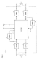
- FIG. 2 is a block diagram illustrating a configuration of a control circuit 3.1 illustrated in FIG. 1.
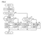
- 3 is a flowchart showing the operation of the internal circuit shown in FIG.
- FIG. 3 is a block diagram illustrating a configuration of a control circuit 3.2 illustrated in FIG. 1.
- 5 is a flowchart showing the operation of the internal circuit shown in FIG.
- FIG. 3 is a block diagram illustrating a configuration of a control circuit 3.3 illustrated in FIG. 1.
- 7 is a flowchart showing the operation of the internal circuit shown in FIG.
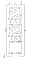
- FIG. 3 is a circuit block diagram showing communication paths in the control circuits 3.1 to 3.3 shown in FIG. FIG.
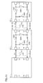
- FIG. 3 is a circuit block diagram showing another communication path in the control circuits 3.1 to 3.3 shown in FIG.
- FIG. 6 is a circuit block diagram showing still another communication path in the control circuits 3.1 to 3.3 shown in FIG.
- FIG. 6 is a circuit block diagram showing still another communication path in the control circuits 3.1 to 3.3 shown in FIG.
- FIG. 1 is a circuit block diagram showing a configuration of a power conversion system according to an embodiment of the present invention.
- this power conversion system includes a plurality (three in the figure) of inverters 1.1 to 1.3, a plurality (three in this case) of current detectors 2.1 to 2.3, A plurality (three in this case) of control circuits 3.1 to 3.3 and a plurality (three in this case) of communication cables 4.1 to 4.3 are provided.
- Each of inverters 1.1 to 1.3 constitutes an electric device, and control circuits 3.1 to 3.3 and communication cables 4.1 to 4.3 constitute a control system.
- Inverters 1.1 to 1.3 operate based on control signals CNT1 to CNT3 from control circuits 3.1 to 3.3, respectively, and supply DC voltages supplied from DC power supplies 5.1 to 5.3, respectively. Convert to an AC voltage of a certain frequency (for example, commercial frequency). Output voltages of the inverters 1.1 to 1.3 are applied to the load 6 in parallel.
- Each of DC power supplies 5.1 to 5.3 may be a battery, a capacitor, or a converter that converts AC power into DC power.
- the control circuits 3.1 and 3.2 are connected to the control circuits 3.2 and 3.3 at the subsequent stages via the communication cables 4.1 and 4.2, respectively.
- the control circuit 3.3 is connected to the communication cable 4.3.
- the previous stage of the control circuit 3.1 is the control circuit 3.3
- the subsequent stage of the control circuit 3.1 is the control circuit 3.2.
- the previous stage of the control circuit 3.2 is the control circuit 3.1
- the subsequent stage of the control circuit 3.2 is the control circuit 3.3.
- the previous stage of the control circuit 3.3 is the control circuit 3.2, and the subsequent stage of the control circuit 3.3 is the control circuit 3.1.
- the control circuits 3.1 to 3.3 are connected in a ring shape by communication cables 4.1 to 4.3, and exchange data signals with each other via the communication cables 4.1 to 4.3.
- the control circuit 3.1 is a master, and each of the control circuits 3.2 and 3.3 is a slave.
- the control circuit 3.1 has a load current value IL1 indicated by the output signal ⁇ 1 of the current detector 2.1 and a load current value IL2, indicated by the data signals D2 and D3 from the control circuits 3.2 and 3.3.
- control circuit 3.1 gradually delays the phase of the output voltage of the inverter 1.1 when the cross current IC1 has a positive value, and outputs the output voltage of the inverter 1.1 when the cross current IC1 has a negative value.
- the phase of is gradually advanced.
- the control circuit 3.1 transmits a data signal D1 indicating the obtained shared current IS to the control circuits 3.2 and 3.3.
- the data signal D1 is a signal for controlling the inverters 1.1 to 1.3.
- the control signal CNT2 is generated to control the inverter 1.2 so that the obtained cross current IC2 becomes 0A.
- the control circuit 3.2 transmits a data signal D2 indicating the load current value IL2 detected by the current detector 2.2 to the control circuit 3.1.
- the data signal D2 is a signal indicating the control result of the inverter 1.2.
- the control circuit 3.2 outputs an alarm signal AL2 that notifies that fact.
- a light source, a sound source, a display, or the like may be provided for notifying that an abnormality has occurred in the communication of the data signal by light, sound, image, or the like.
- the control signal CNT3 is generated and the inverter 1.3 is controlled so that the obtained cross current IC3 becomes 0A.
- the control circuit 3.3 transmits a data signal D3 indicating the load current value IL3 detected by the current detector 2.3 to the control circuit 3.1.
- the data signal D3 is a signal indicating the control result of the inverter 1.3.
- the control circuit 3.3 outputs an alarm signal AL3 that notifies that fact.
- a light source, a sound source, a display, or the like may be provided for notifying that an abnormality has occurred in the communication of the data signal by light, sound, image, or the like.
- the communication cable 4.1 is connected between the control circuits 3.1 and 3.2, and a communication line L1 for transmitting a data signal from the preceding control circuit 3.1 to the succeeding control circuit 3.2; Communication line L2 for transmitting a data signal from control circuit 3.2 to control circuit 3.1 in the previous stage.
- the communication cable 4.2 is connected between the control circuits 3.2 and 3.3, and a communication line L1 for transmitting a data signal from the control circuit 3.2 at the previous stage to the control circuit 3.3 at the rear stage, and the rear stage.
- Communication line L2 for transmitting a data signal from control circuit 3.3 to control circuit 3.2 in the preceding stage.
- the communication cable 4.3 is connected between the control circuits 3.3 and 3.1, and a communication line L1 for transmitting a data signal from the control circuit 3.3 at the front stage to the control circuit 3.1 at the rear stage, and the rear stage. And a communication line L2 for transmitting a data signal from the control circuit 3.1 to the previous control circuit 3.3.
- the communication cable 4.1 is a multi-core cable.
- Each of the communication lines L1 to L3 includes a plurality of signal lines. Connectors (not shown) are provided at each of one end and the other end of the communication cable 4.1.
- Each of the communication cables 4.2 and 4.3 has the same configuration as the communication cable 4.1.
- the connector at one end of the communication cable 4.1 is connected to the connector of the control circuit 3.1, and the connector at the other end of the communication cable 4.1 is connected to the connector of the control circuit 3.2.
- the connector at one end of the communication cable 4.2 is connected to the connector of the control circuit 3.2, and the connector at the other end of the communication cable 4.2 is connected to the connector of the control circuit 3.3.
- the connector at one end of the communication cable 4.3 is connected to the connector of the control circuit 3.3, and the connector at the other end of the communication cable 4.3 is connected to the connector of the control circuit 3.1.
- control circuits 3.1, 3.2, 3.2, 3.3, 3.3, and 3.1 When data signals are normally communicated between the control circuits 3.1, 3.2, 3.2, 3.3, 3.3, and 3.1, the control circuits 3.1 to 3.3 and the communication line L1 of the communication cables 4.1 to 4.3 form an annular first communication path, and the control circuits 3.1 to 3.3 and the communication cables 4.1 to 4.3.
- An annular second communication path is formed by the communication line L2.
- the data signal D1 is transmitted from the control circuit 3.1 to the control circuit 3.2 via the communication line L1 of the communication cable 4.1, and from the control circuit 3.2 to the communication cable 4.2.
- Data signals D1 and D2 are transmitted to the control circuit 3.3 via the communication line L1
- the data signals D1 to D3 are transmitted from the control circuit 3.3 to the control circuit 3.1 via the communication line L1 of the communication cable 4.3. Is sent.
- the data signal D1 is transmitted from the control circuit 3.1 to the control circuit 3.3 via the communication line L2 of the communication cable 4.3, and from the control circuit 3.3 to the communication cable 4.2.
- Data signals D1 and D3 are transmitted to the control circuit 3.2 via the communication line L2, and the data signals D1 to D3 are transmitted from the control circuit 3.2 to the control circuit 3.1 via the communication line L2 of the communication cable 4.1. Is sent.
- the data signal D1 is transmitted from the control circuit 3.1 to the control circuit 3.3 via the communication line L2 of the communication cable 4.3, and from the control circuit 3.3 to the communication cable 4.2.
- Data signals D1 and D3 are transmitted to the control circuit 3.2 via the communication line L2, and the data signals D1 to D3 are transmitted from the control circuit 3.2 to the control circuit 3.3 via the communication line L1 of the communication cable 4.2.
- the data signals D1 to D3 are transmitted from the control circuit 3.3 to the control circuit 3.1 via the communication line L1 of the communication cable 4.3.
- control circuit 3.1 to 3.3 and the communication cables 4.1 and 4.3 use the annular fourth signal. Communication paths are formed.
- the data signal D1 is transmitted from the control circuit 3.1 to the control circuit 3.3 via the communication line L2 of the communication cable 4.3, and the control circuit 3.3 transmits the communication cable 4.3.
- Data signals D1, D3 are transmitted to the control circuit 3.1 via the communication line L1
- the data signals D1, D3 are transmitted from the control circuit 3.1 to the control circuit 3.2 via the communication line L1 of the communication cable 4.1.
- the data signals D1 to D3 are transmitted from the control circuit 3.2 to the control circuit 3.1 via the communication line L2 of the communication cable 4.1.
- control circuit 3.1 If the data signal is not normally transmitted between the control circuit 3.3 and the control circuit 3.1, the control circuit 3.1 to 3.3 and the communication cables 4.1 and 4.2 are connected to the annular fifth Communication paths are formed.
- the data signal D1 is transmitted from the control circuit 3.1 to the control circuit 3.2 via the communication line L1 of the communication cable 4.1, and from the control circuit 3.2 to the communication cable 4.2.
- Data signals D1 and D2 are transmitted to the control circuit 3.3 via the communication line L1
- the data signals D1 to D3 are transmitted from the control circuit 3.3 to the control circuit 3.2 via the communication line L2 of the communication cable 4.2.
- the data signals D1 to D3 are transmitted from the control circuit 3.2 to the control circuit 3.1 via the communication line L2 of the communication cable 4.1.
- FIG. 2 is a block diagram showing the configuration of the control circuit 3.1.
- the control circuit 3.1 includes receivers 11 and 12, transmitters 13 and 14, determiners 15 and 16, and an internal circuit 17.
- the receiver 11 receives the data signals D1 to D3 transmitted from the control circuit 3.3 via the communication line L1 of the communication cable 4.3, and receives the received data signals D1 to D3 by the determiner 15 and the internal circuit 17. To give.
- the determiner 15 determines whether or not the data signals D1 to D3 from the receiver 11 are normal. If the data signals D1 to D3 are normal, the signal ⁇ 15 is set to “L” level, and the data signal When D1 to D3 are abnormal, signal ⁇ 15 is set to “H” level. Signal ⁇ 15 is applied to internal circuit 17.
- the receiver 12 receives the data signals D1 to D3 transmitted from the control circuit 3.2 via the communication line L2 of the communication cable 4.1, and receives the received data signals D1 to D3 from the determiner 16 and the internal circuit 17. To give.
- the determiner 16 determines whether or not the data signals D1 to D3 from the receiver 12 are normal. If the data signals D1 to D3 are normal, the signal ⁇ 16 is set to “L” level, and the data signal When D1 to D3 are abnormal, signal ⁇ 16 is set to “H” level. Signal ⁇ 16 is applied to internal circuit 17.
- the determination of whether the data signals D1 to D3 are normal in the determiners 15 and 16 is performed by, for example, a parity check method.
- a parity check method a bit string that constitutes a data signal is divided into fixed units, and parity bits indicating whether the number of bits having a value “1” included in each unit is an odd number or an even number is included. Attached to each unit. On the receiving side, the number of “1” and the parity bit are compared for each unit, and it is detected whether or not an error has occurred during data transmission. Further, it may be determined whether or not the data size is normal, or a method described in Japanese Patent Laid-Open No. 2006-340082 (Patent Document 2) may be employed.
- the internal circuit 17 determines that the data signals D1 to D3 are normal by the determiners 15 and 16, the signals ⁇ 15 and ⁇ 16 are both set to the “L” level, and receives the data signals D2 and D3 from the receiver 11.
- the received data signals D2 and D3 that is, load current values IL2 and IL3
- the output signal ⁇ 1 of the current detector 2.1 that is, load current
- a new data signal D1 that is, a shared current value IS for controlling the inverters 2.1 to 2.3 is generated.
- the internal circuit 17 stores the latest data signals D2 and D3 used to generate the data signal D1 when the data communication is normally performed as described above.
- the internal circuit 17 determines that the data signals D1 to D3 are normal by the determiners 15 and 16, and the data signals D1 to D3 from the receiver 11 and the data signals D1 to D3 from the receiver 12 are equal to each other. If not, the latest data signals D2 and D3 (that is, load current values IL2 and IL3) that are used and stored when data communication is normally performed and the output signal ⁇ 1 of the current detector 2.1 (that is, the current signal 2.1) Based on the load current value IL1), a new data signal D1 (that is, a shared current value IS) for controlling the inverters 2.1 to 2.3 is generated.
- the internal circuit 17 determines that the data signal D1 to D3 from the receiver 11 is normal by the determiner 15 and sets the signal ⁇ 15 to the “L” level, and the data signal D1 from the receiver 12 by the determiner 16
- D3 is determined to be abnormal and the signal ⁇ 16 is set to the “H” level
- the data signals D2 and D3 that is, load current values IL2 and IL3
- the output signal ⁇ 1 that is, the load current value IL1
- a new data signal D1 that is, the shared current value IS for controlling the inverters 2.1 to 2.3 is generated.
- the internal circuit 17 determines that the data signal D1 to D3 from the receiver 11 is abnormal by the determiner 15 and sets the signal ⁇ 15 to the “H” level, and the data signal D1 from the receiver 12 by the determiner 16
- D3 is determined to be normal and the signal ⁇ 16 is set to “L” level
- the data signals D2 and D3 that is, load current values IL2 and IL3
- the output signal ⁇ 1 that is, the load current value IL1
- a new data signal D1 that is, the shared current value IS for controlling the inverters 2.1 to 2.3 is generated.
- the internal circuit 17 uses the latest data signals D2 and D3 (used and stored when data communication is normally performed). That is, a new data signal D1 (for controlling the inverters 2.1 to 2.3 based on the load current values IL2 and IL3) and the output signal ⁇ 1 of the current detector 2.1 (that is, the load current value IL1). That is, a shared current value IS) is generated.
- the control signal CNT1 is generated so that the cross current IC becomes 0A to control the inverter 1.1.
- the transmitter 13 transmits a new data signal D1 generated by the internal circuit 17 to the control circuit 3.2 via the communication line L1 of the communication cable 4.1.
- the transmitter 14 transmits a new data signal D1 generated by the internal circuit 17 to the control circuit 3.3 via the communication line L2 of the communication cable 4.3.
- FIG. 3 is a flowchart showing the operation of the internal circuit 17.
- the internal circuit 17 receives the data signals D1 to D3 via the receivers 11 and 12.
- the internal circuit 17 determines whether or not the output signals ⁇ 15 and ⁇ 16 of the determiners 15 and 16 are both at the “L” level.
- the internal circuit 17 determines that the data signals D2 and D3 from the receiver 11 match the data signals D2 and D3 from the receiver 12 in step S3. It is determined whether or not.
- step S3 If it is determined in step S3 that the data signals D2 and D3 from the receivers 11 and 12 match, the internal circuit 17 processes using the data signals D2 and D3 from the receivers 11 and 12 in step S4. . That is, the internal circuit 17 generates a new data signal D1 based on the received data signals D2 and D3 and the output signal ⁇ 1 of the current detector 2.1, and sends the new data signal D1 to the control circuit 3.2, 2. 3.3, the latest data signals D2 and D3 used to generate the data signal D1 are stored, the inverter 1.1 is controlled using the new data signal D1, and the process returns to step S1.
- step S5 uses the latest stored and used when data communication is normally performed. Processing is performed using the data signals D2 and D3. That is, the internal circuit 17 generates a new data signal D1 based on the latest data signals D2 and D3 and the output signal ⁇ 1 of the current detector 2.1 that are used and stored when data communication is normally performed. The new data signal D1 is generated and transmitted to the control circuits 3.2 and 3.3, and the inverter 1.1 is controlled using the new data signal D1, and the process returns to step S1.
- step S2 When the condition that the signals ⁇ 15 and ⁇ 16 are both at the “L” level is denied in step S2, the internal circuit 17 determines whether the signal ⁇ 15 or the signal ⁇ 16 is at the “L” level in step S6.
- step S7 the internal circuit 17 determines that the normal data signal D1 of the data signals D1 to D3 from the receivers 11 and 12 is correct. Process using data signals D2 and D3 included in D3. That is, the internal circuit 17 generates a new data signal D1 based on the normal data signals D2 and D3 and the output signal ⁇ 1 of the current detector 2.1, and the new data signal D1 is transmitted to the control circuit 3. 2 and 3.3, control the inverter 1.1 using the new data signal D1, and return to step S1.
- the internal circuit 17 uses the latest data signal stored and used when the data communication is normally performed in step S8. Process using D2 and D3. That is, the internal circuit 17 generates a new data signal D1 based on the latest data signals D2 and D3 and the output signal ⁇ 1 of the current detector 2.1 that are used and stored when data communication is normally performed. The new data signal D1 is generated and transmitted to the control circuits 3.2 and 3.3, and the inverter 1.1 is controlled using the new data signal D1, and the process returns to step S1.
- FIG. 4 is a block diagram showing the configuration of the control circuit 3.2, and is a diagram contrasted with FIG. Referring to FIG. 4, control circuit 3.2 is different from control circuit 3.1 in that abnormality detectors 21 and 222 are added and internal circuit 17 is replaced by internal circuit 23.
- the receiver 11 receives the data signal D1 transmitted from the control circuit 3.1 via the communication line L1 of the communication cable 4.1, and gives the received data signal D1 to the determination unit 15 and the internal circuit 23.
- the determiner 15 determines whether or not the data signal D1 from the receiver 11 is normal. If the data signal D1 is normal, the signal ⁇ 15 is set to “L” level, and the data signal D1 is abnormal. In some cases, signal ⁇ 15 is set to “H” level. Signal ⁇ 15 is applied to internal circuit 23.
- the receiver 12 receives the data signals D1 and D3 transmitted from the control circuit 3.3 via the communication line L2 of the communication cable 4.2, and receives the received data signals D1 and D3 by the determiner 16 and the internal circuit 17. To give.
- the determiner 16 determines whether or not the data signals D1 and D3 from the receiver 12 are normal. If the data signals D1 and D3 are normal, the signal ⁇ 16 is set to “L” level, and the data signal When D1 and D3 are abnormal, signal ⁇ 16 is set to “H” level. Signal ⁇ 16 is applied to internal circuit 23.
- the abnormality detector 21 turns the abnormality detection signal ⁇ 21 into the inactivation level “L”. It rises from the level to the activation level “H” level.
- the abnormality detector 22 sets the abnormality detection signal ⁇ 22 to the inactivation level “L”. It rises from the level to the activation level “H” level.
- Internal circuit 23 determines that data signals D1 and data signals D1 and D3 are normal by determiners 15 and 16, both signals ⁇ 15 and ⁇ 16 are set to the “L” level, and data signal D1 from receiver 11 And the data signal D1 from the receiver 12 coincide with each other in the data signal D1 (that is, the shared current value IS) and the output signal ⁇ 2 (that is, the load current value IL2) of the current detector 2.2. Based on this, the cross current IC2 is obtained, and the control signal CNT2 is generated to control the inverter 1.2 so that the cross current IC2 becomes 0A.
- the internal circuit 23 generates a data signal D2 (that is, a load current value IL2) based on the output signal ⁇ 2 of the current detector 2.2.
- the internal circuit 23 stores the latest data signal D1 used for controlling the inverter 1.2 when the data communication is normally performed as described above.
- the internal circuit 23 determines that the data signal D1 and the data signals D1 and D3 are normal by the determiners 15 and 16, and the data signal D1 from the receiver 11 and the data signal D1 from the receiver 12 are equal to each other. If not, the latest data signal D1 (that is, the shared current value IS) that is used and stored when the data communication is normally performed and the output signal ⁇ 2 (that is, the load current value IL2) of the current detector 2.2 are stored. ) And the control signal CNT2 is generated so that the cross current IC2 becomes 0A to control the inverter 1.2. Furthermore, the internal circuit 23 generates a data signal D2 (that is, a load current value IL2) based on the output signal ⁇ 2 of the current detector 2.2.
- the internal circuit 23 determines that the data signal D1 from the receiver 11 is normal by the determiner 15 and sets the signal ⁇ 15 to “L” level, and the data signal D1, D3 from the receiver 12 by the determiner 16 Is determined to be abnormal and the signal ⁇ 16 is set to the “H” level, the data signal D1 from the receiver 11 (ie, the shared current value IS) and the output signal ⁇ 2 of the current detector 2.2 (ie, the load)
- the cross current IC2 is obtained based on the current value IL2), the control signal CNT2 is generated so that the cross current IC2 becomes 0A, and the inverter 1.2 is controlled. Furthermore, the internal circuit 23 generates a data signal D2 (that is, a load current value IL2) based on the output signal ⁇ 2 of the current detector 2.2.
- the internal circuit 23 determines that the data signal D1 from the receiver 11 is abnormal by the determiner 15 and sets the signal ⁇ 15 to the “H” level, and the data signal D1 and D3 from the receiver 12 by the determiner 16 Is determined to be normal and the signal ⁇ 16 is set to the “L” level, the data signal D1 from the receiver 12 (ie, the shared current value IS) and the output signal ⁇ 2 of the current detector 2.2 (ie, the load)
- the cross current IC2 is obtained based on the current value IL2), the control signal CNT2 is generated so that the cross current IC2 becomes 0A, and the inverter 1.2 is controlled. Furthermore, the internal circuit 23 generates a data signal D2 (that is, a load current value IL2) based on the output signal ⁇ 2 of the current detector 2.2.
- the internal circuit 23 uses the latest data signal D1 stored and stored when data communication is normally performed (ie, sharing). Current IS) and output signal ⁇ 2 of current detector 2.2 (that is, load current value IL2), cross current IC2 is obtained, control signal CNT2 is generated so that cross current IC2 becomes 0A, and inverter 1.2 To control. Furthermore, the internal circuit 23 generates a data signal D2 (that is, a load current value IL2) based on the output signal ⁇ 2 of the current detector 2.2.
- the internal circuit 23 includes switches SW1 to SW4.
- the switch SW1 is connected between the receiver 11 and the transmitter 13.
- the switch SW2 is connected between the receiver 12 and the transmitter 14.
- the switch SW3 is connected between the receiver 11 and the transmitter 14.
- the switch SW4 is connected between the receiver 12 and the transmitter 13.
- the internal circuit 23 provides the data signal D1 and the new data signal D2 from the receiver 11 to the transmitter 13 via the switch SW1, and the data signals D1 and D3 from the receiver 12 and the new data signal D2 To the transmitter 14 via the switch SW2.
- the transmitter 13 transmits the data signals D1, D2 from the internal circuit 23 to the control circuit 3.2 via the communication line L1 of the communication cable 4.2.
- the transmitter 14 transmits the data signals D1 to D3 from the internal circuit 23 to the control circuit 3.1 via the communication line L2 of the communication cable 4.1.
- the switch SW4 When the abnormality detection signals ⁇ 21 and ⁇ 22 become “H” level and “L” level, respectively, the switch SW4 is turned on and the switches SW1 to SW3 are turned off.
- the internal circuit 23 stops the reception of the data signal D1 from the receiver 11, and supplies the data signals D1 and D3 and the new data signal D2 from the receiver 12 to the transmitter 13 via the switch SW4.
- the transmitter 13 transmits the data signals D1 to D3 from the internal circuit 23 to the control circuit 3.2 via the communication line L1 of the communication cable 4.2. Transmission of the data signal from the transmitter 14 is stopped.
- the switch SW3 When the abnormality detection signals ⁇ 21, ⁇ 22 become “L” level and “H” level, respectively, the switch SW3 is turned on and the switches SW1, SW2, SW4 are turned off.
- the internal circuit 23 stops receiving the data signals D1 and D3 from the receiver 12, and supplies the data signal D1 and the new data signal D2 from the receiver 11 to the transmitter 14 via the switch SW3.
- the transmitter 14 transmits the data signals D1, D2 from the internal circuit 23 to the control circuit 3.1 via the communication line L2 of the communication cable 4.1. Transmission of the data signal from the transmitter 13 is stopped.
- the output signals ⁇ 15 and ⁇ 16 of the determiners 15 and 16 are both at the “L” level, the data signal D1 from the receiver 11 and the data signal D1 from the receiver 12 do not coincide with each other three times in succession.
- the switch SW3 is turned on and the switches SW1, SW2 and SW4 are turned off.
- the internal circuit 23 stops receiving the data signals D1 and D3 from the receiver 12, and supplies the data signal D1 and the new data signal D2 from the receiver 11 to the transmitter 14 via the switch SW3.
- the transmitter 14 transmits the data signals D1, D2 from the internal circuit 23 to the control circuit 3.1 via the communication line L2 of the communication cable 4.1. Transmission of the data signal from the transmitter 13 is stopped.
- the internal circuit 23 outputs an alarm signal AL2 for notifying that an abnormality has occurred in data signal communication.
- the output signals ⁇ 15 and ⁇ 16 of the determiners 15 and 16 are both at the “L” level, it is continuously 3 that the data signal D1 from the receiver 11 and the data signal D1 from the receiver 12 do not match. If this occurs, the switch SW4 may be turned on and the switches SW1 to SW3 may be turned off.
- the internal circuit 23 stops the reception of the data signal D1 from the receiver 11, and supplies the data signals D1 and D3 and the new data signal D2 from the receiver 12 to the transmitter 13 via the switch SW4.
- the transmitter 13 transmits the data signals D1 to D3 from the internal circuit 23 to the control circuit 3.2 via the communication line L1 of the communication cable 4.2. Transmission of the data signal from the transmitter 14 is stopped.
- FIG. 5 is a flowchart showing the operation of the internal circuit 23.
- the internal circuit 23 receives the data signals D ⁇ b> 1 and D ⁇ b> 3 via the receivers 11 and 12.
- the internal circuit 23 determines whether or not the output signals ⁇ 15 and ⁇ 16 of the determiners 15 and 16 are both at the “L” level.
- the internal circuit 23 determines whether the data signal D1 from the receiver 11 and the data signal D1 from the receiver 12 match in step S13. Is determined.
- step S13 If it is determined in step S13 that the data signals D1 from the receivers 11 and 12 match, the internal circuit 23 processes using the data signals D1 from the receivers 11 and 12 in step S14. That is, the internal circuit 23 controls the inverter 1.2 based on the received data signal D1 and the output signal ⁇ 2 of the current detector 2.2, stores the latest data signal D1, and based on the signal ⁇ 2. A new data signal D2 is generated and transmitted to the control circuits 3.1 and 3.3, and the process returns to step S11.
- step S15 the internal circuit 23 uses the latest data signal stored and used when data communication is normally performed. Process using D1. That is, internal circuit 23 controls inverter 1.2 based on the latest data signal D1 used and stored when data communication is normally performed and output signal ⁇ 2 of current detector 2.2. A new data signal D2 is generated based on the signal ⁇ 2 and transmitted to the control circuits 3.1 and 3.3.
- step S16 the internal circuit 23 determines whether or not the data signal D1 when data communication is normally performed has been used three times in succession. If it is determined in step S16 that the data signal D1 when the data communication is normally performed is used three times continuously, the internal circuit 23 switches the switches SW1 to SW4 in step S17 and outputs the alarm signal AL2. Output and return to step S11. At that time, the switch SW3 is turned on and the switches SW1, SW2, and SW4 are turned off. In step S16, when the condition that the data signal D1 when the communication is normally performed is used continuously three times is denied, the processing by the internal circuit 23 returns to step S11.
- step S12 If the condition that both the signals ⁇ 15 and ⁇ 16 are at “L” level is denied in step S12, the internal circuit 23 determines whether the signal ⁇ 15 or the signal ⁇ 16 is at “L” level in step S18.
- the internal circuit 23 uses the normal data signal D1 of the data signals D1 from the receivers 11 and 12 in step S19. To process. That is, the internal circuit 23 controls the inverter 1.2 based on the normal data signal D1 and the output signal ⁇ 2 of the current detector 2.2, and generates a new data signal D2 based on the signal ⁇ 2. Then, the data is transmitted to the control circuits 3.1 and 3.3 and the process proceeds to step S21.
- the internal circuit 23 uses the latest data signal stored and used when data communication is normally performed in step S20. Process using D1. That is, internal circuit 23 controls inverter 1.2 based on the latest data signal D1 used and stored when data communication is normally performed and output signal ⁇ 2 of current detector 2.2. Then, a new data signal D2 is generated based on the signal ⁇ 2 and transmitted to the control circuits 3.1 and 3.3, and the process proceeds to step S21.
- step S21 the internal circuit 23 determines whether or not the abnormality detection signal ⁇ 21 or ⁇ 22 is at “H” level. If the abnormality detection signal ⁇ 21 or ⁇ 22 is at “H” level, the switches SW1 to SW4 are switched in step S22. And an alarm signal AL2 is output, and the process returns to step S11. At this time, when the abnormality detection signal ⁇ 21 is at “H” level, the switches SW1 to SW3 are turned off and the switch SW4 is turned on. When the abnormality detection signal ⁇ 22 is at “H” level, the switches SW1 and SW2 are turned on. , SW4 are turned off and the switch SW3 is turned on. If the condition that the abnormality detection signal ⁇ 21 or ⁇ 22 is at “H” level is denied in step S21, the processing by the internal circuit 23 returns to step S11.
- FIG. 6 is a block diagram showing the configuration of the control circuit 3.3, and is a diagram contrasted with FIG. Referring to FIG. 6, control circuit 3.3 is different from control circuit 3.2 in that internal circuit 23 is replaced by internal circuit 24.
- the receiver 11 receives the data signals D1 and D2 transmitted from the control circuit 3.2 via the communication line L1 of the communication cable 4.2, and receives the received data signals D1 and D2 by the determiner 15 and the internal circuit 23. To give.
- the determiner 15 determines whether or not the data signals D1 and D2 from the receiver 11 are normal. If the data signals D1 and D2 are normal, the determiner 15 sets the signal ⁇ 15 to the “L” level, and the data signal When D1 and D2 are abnormal, signal ⁇ 15 is set to “H” level. Signal ⁇ 15 is applied to internal circuit 24.
- the receiver 12 receives the data signal D1 transmitted from the control circuit 3.1 via the communication line L2 of the communication cable 4.3, and gives the received data signal D1 to the determiner 16 and the internal circuit 17.
- the determiner 16 determines whether or not the data signal D1 from the receiver 12 is normal. If the data signal D1 is normal, the signal ⁇ 16 is set to “L” level, and the data signal D1 is abnormal. In some cases, signal ⁇ 16 is set to “H” level. Signal ⁇ 16 is applied to internal circuit 24.
- the operation of the abnormality detectors 21 and 22 is as described with reference to FIG.
- the internal circuit 24 determines that the data signals D1 and D2 and the data signal D1 are normal by the determiners 15 and 16, both the signals ⁇ 15 and ⁇ 16 are set to the “L” level, and the data signal D1 from the receiver 11 And the data signal D1 from the receiver 12 coincide with each other in the data signal D1 (that is, the shared current value IS) and the output signal ⁇ 3 (that is, the load current value IL3) of the current detector 2.3. Based on this, the cross current IC3 is obtained, and the control signal CNT3 is generated to control the inverter 1.3 so that the cross current IC3 becomes 0A.
- the internal circuit 24 generates a data signal D3 (that is, a load current value IL3) based on the output signal ⁇ 3 of the current detector 2.3.
- the internal circuit 24 stores the latest data signal D1 used for controlling the inverter 1.3 when the data communication is normally performed as described above.
- the internal circuit 24 determines that the data signals D1, D2 and the data signal D1 are normal by the determiners 15 and 16, and the data signal D1 from the receiver 11 and the data signal D1 from the receiver 12 are equal to each other. If not, the latest data signal D1 (that is, the shared current value IS) that is used and stored when the data communication is normally performed and the output signal ⁇ 3 (that is, the load current value IL3) of the current detector 2.3 are stored. ) And the control signal CNT3 is generated to control the inverter 1.3 so that the cross current IC3 becomes 0A. Furthermore, the internal circuit 24 generates a data signal D3 (that is, a load current value IL3) based on the output signal ⁇ 3 of the current detector 2.3.
- the internal circuit 24 determines that the data signal D1, D2 from the receiver 11 is normal by the determiner 15 and sets the signal ⁇ 15 to the “L” level, and the data signal D1 from the receiver 12 by the determiner 16 Is determined to be abnormal and the signal ⁇ 16 is set to the “H” level, the data signal D1 from the receiver 11 (ie, the shared current value IS) and the output signal ⁇ 3 of the current detector 2.3 (ie, the load)
- the cross current IC3 is obtained based on the current value IL3), the control signal CNT3 is generated so that the cross current IC3 becomes 0A, and the inverter 1.3 is controlled. Furthermore, the internal circuit 24 generates a data signal D3 (that is, a load current value IL3) based on the output signal ⁇ 3 of the current detector 2.3.
- the internal circuit 24 determines that the data signal D1, D2 from the receiver 11 is abnormal by the determiner 15 and sets the signal ⁇ 15 to the “H” level, and the data signal D1 from the receiver 12 by the determiner 16 Is determined to be normal and the signal ⁇ 16 is set to the “L” level, the data signal D1 from the receiver 12 (ie, the shared current value IS) and the output signal ⁇ 3 of the current detector 2.3 (ie, the load)
- the cross current IC3 is obtained based on the current value IL3), the control signal CNT3 is generated so that the cross current IC3 becomes 0A, and the inverter 1.3 is controlled. Furthermore, the internal circuit 24 generates a data signal D3 (that is, a load current value IL3) based on the output signal ⁇ 3 of the current detector 2.3.
- the internal circuit 24 uses the latest data signal D1 stored and stored when the data communication is normally performed (that is, sharing). Current IS) and output signal ⁇ 3 of current detector 2.3 (that is, load current value IL3), cross current IC3 is obtained, and control signal CNT3 is generated so that cross current IC3 becomes 0A to generate inverter 1.3. To control. Furthermore, the internal circuit 24 generates a data signal D3 (that is, a load current value IL3) based on the output signal ⁇ 3 of the current detector 2.3.
- the internal circuit 24 includes switches SW1 to SW4.
- the switch SW1 is connected between the receiver 11 and the transmitter 13.
- the switch SW2 is connected between the receiver 12 and the transmitter 14.
- the switch SW3 is connected between the receiver 11 and the transmitter 14.
- the switch SW4 is connected between the receiver 12 and the transmitter 13.
- the internal circuit 24 supplies the data signals D1 and D2 and the new data signal D3 from the receiver 11 to the transmitter 13 via the switch SW1, and the data signal D1 and the new data signal D3 from the receiver 12 To the transmitter 14 via the switch SW2.
- the transmitter 13 transmits the data signals D1 to D3 from the internal circuit 23 to the control circuit 3.1 via the communication line L1 of the communication cable 4.3.
- the transmitter 14 transmits the data signals D1, D3 from the internal circuit 24 to the control circuit 3.2 via the communication line L2 of the communication cable 4.2.
- the switch SW4 is turned on and the switches SW1 to SW3 are turned off.
- the internal circuit 24 stops receiving the data signals D1 and D2 from the receiver 11, and supplies the data signals D1 and D3 and the new data signal D2 from the receiver 12 to the transmitter 13 via the switch SW4. .
- the transmitter 13 transmits the data signals D1 to D3 from the internal circuit 24 to the control circuit 3.1 via the communication line L1 of the communication cable 4.3. Transmission of the data signal from the transmitter 14 is stopped.
- the switch SW3 When the abnormality detection signals ⁇ 21, ⁇ 22 become “L” level and “H” level, respectively, the switch SW3 is turned on and the switches SW1, SW2, SW4 are turned off.
- the internal circuit 24 stops receiving the data signal D1 from the receiver 12, and supplies the data signals D1, D2 and the new data signal D3 from the receiver 11 to the transmitter 14 via the switch SW3.
- the transmitter 14 transmits the data signals D1 to D3 from the internal circuit 24 to the control circuit 3.2 via the communication line L2 of the communication cable 4.2. Transmission of the data signal from the transmitter 13 is stopped.
- the output signals ⁇ 15 and ⁇ 16 of the determiners 15 and 16 are both at the “L” level, the data signal D1 from the receiver 11 and the data signal D1 from the receiver 12 do not coincide with each other three times in succession.
- the switch SW3 is turned on and the switches SW1, SW2 and SW4 are turned off.
- the internal circuit 24 stops receiving the data signal D1 from the receiver 12, and supplies the data signals D1, D2 and the new data signal D3 from the receiver 11 to the transmitter 14 via the switch SW3.
- the transmitter 14 transmits the data signals D1 to D3 from the internal circuit 24 to the control circuit 3.1 via the communication line L2 of the communication cable 4.1. Transmission of the data signal from the transmitter 13 is stopped.
- the internal circuit 23 outputs an alarm signal AL3 notifying that an abnormality has occurred in the data signal.
- the output signals ⁇ 15 and ⁇ 16 of the determiners 15 and 16 are both at the “L” level, it is continuously 3 that the data signal D1 from the receiver 11 and the data signal D1 from the receiver 12 do not match. If this occurs, the switch SW4 may be turned on and the switches SW1 to SW3 may be turned off.
- the internal circuit 24 stops receiving the data signals D1 and D2 from the receiver 11, and supplies the data signal D1 and the new data signal D3 from the receiver 12 to the transmitter 13 via the switch SW4.
- the transmitter 13 transmits the data signals D1, D3 from the internal circuit 24 to the control circuit 3.1 via the communication line L1 of the communication cable 4.2. Transmission of the data signal from the transmitter 14 is stopped.
- FIG. 7 is a flowchart showing the operation of the internal circuit 24.
- the internal circuit 24 receives the data signals D1, D2 via the receivers 11, 12.
- the internal circuit 24 determines whether or not the output signals ⁇ 15 and ⁇ 16 of the determiners 15 and 16 are both at the “L” level.
- the internal circuit 24 determines whether the data signal D1 from the receiver 11 and the data signal D1 from the receiver 12 match in step S33. Is determined.
- step S33 If it is determined in step S33 that the data signals D1 from the receivers 11 and 12 match, the internal circuit 24 processes the data signals D1 from the receivers 11 and 12 in step S34. That is, the internal circuit 24 controls the inverter 1.3 based on the received data signal D1 and the output signal ⁇ 3 of the current detector 2.3, stores the latest data signal D1, and based on the signal ⁇ 3. A new data signal D3 is generated and transmitted to the control circuits 3.1 and 3.2, and the process returns to step S31.
- step S35 the internal circuit 24 uses the latest data signal stored and used when data communication is normally performed. Process using D1. That is, the internal circuit 24 controls the inverter 1.3 based on the latest data signal D1 used and stored when data communication is normally performed and the output signal ⁇ 3 of the current detector 2.3. A new data signal D3 is generated based on the signal ⁇ 3 and transmitted to the control circuits 3.1 and 3.2.
- step S36 the internal circuit 24 determines whether or not the data signal D1 when data communication is normally performed is used three times in succession.
- step S37 the internal circuit 24 switches the switches SW1 to SW4 and outputs the alarm signal AL2. Output, and return to step S31.
- the switch SW3 is turned on and the switches SW1, SW2, and SW4 are turned off.
- step S36 when the condition that the data signal D1 when the communication is normally performed is used continuously three times is denied, the processing by the internal circuit 24 returns to step S31.
- step S32 the internal circuit 24 determines whether or not the signal ⁇ 15 or the signal ⁇ 16 is “L” level in step S38.
- step S38 If it is determined in step S38 that the signal ⁇ 15 or the signal ⁇ 16 is at the “L” level, the internal circuit 24 uses the normal data signal D1 of the data signals D1 from the receivers 11 and 12 in step S39. To process. That is, the internal circuit 24 controls the inverter 1.3 based on the normal data signal D1 and the output signal ⁇ 3 of the current detector 2.3, and generates a new data signal D3 based on the signal ⁇ 3. Then, the data is transmitted to the control circuits 3.1 and 3.2, and the process proceeds to step S41.
- the internal circuit 24 uses the latest data signal D1 stored and used when communication is normally performed in step S40. To process. That is, the internal circuit 24 controls the inverter 1.3 based on the latest data signal D1 used and stored when data communication is normally performed and the output signal ⁇ 3 of the current detector 2.3. Then, a new data signal D3 is generated based on the signal ⁇ 3 and transmitted to the control circuits 3.1 and 3.2, and the process proceeds to step S41.
- step S41 the internal circuit 24 determines whether or not the abnormality detection signal ⁇ 21 or ⁇ 22 is at “H” level. If the abnormality detection signal ⁇ 21 or ⁇ 22 is at “H” level, the switches SW1 to SW4 are switched in step S42. And an alarm signal AL2 is output, and the process returns to step S31. At this time, when the abnormality detection signal ⁇ 21 is at “H” level, the switches SW1 to SW3 are turned off and the switch SW4 is turned on. When the abnormality detection signal ⁇ 22 is at “H” level, the switches SW1 and SW2 are turned on. , SW4 are turned off and the switch SW3 is turned on. When the condition that the abnormality detection signal ⁇ 21 or ⁇ 22 is “H” level is denied in step S41, the processing by the internal circuit 24 returns to step S31.
- FIG. 8 is a circuit showing a communication path when data communication is normally performed between the control circuits 3.1, 3.2, 3.2, 3.3, 3.3, and 3.1. It is a block diagram.
- the switches SW1 and SW2 are turned on and the switches SW3 and SW4 are turned off.
- a first communication path P1 is formed by the control circuit 3.1 to 3.3 and the communication line L1 of the communication cable 4.1 to 4.3, and the control circuit 3.1 to 3.3 and the communication cable 4.
- a second communication path P1 is formed by the communication lines L2 of 1 to 4.3.
- the data signal D1 generated in the control circuit 3.1 is sent to the receiver 11 of the control circuit 3.2 via the transmitter 13 and the communication line L1 of the communication cable 4.1. Sent.
- the data signal D1 received by the receiver 11 of the control circuit 3.2 and the data signal D2 generated in the control circuit 3.2 are transmitted through the switch SW1, the transmitter 13, and the communication line L1 of the communication cable 4.2.
- the data signals D1 and D2 received by the receiver 11 of the control circuit 3.3 and the data signal D3 generated in the control circuit 3.3 are the switch SW1, the transmitter 13, and the communication line of the communication cable 4.3. It is transmitted to the receiver 11 of the control circuit 3.1 via L1.
- the data signal D1 generated in the control circuit 3.1 is transmitted to the receiver 12 of the control circuit 3.3 via the transmitter 14 and the communication line L2 of the communication cable 4.3. Sent.
- the data signal D1 received by the receiver 12 of the control circuit 3.3 and the data signal D3 generated in the control circuit 3.3 are transmitted through the switch SW2, the transmitter 14, and the communication line L2 of the communication cable 4.2.
- the data signals D1, D3 received by the receiver 12 of the control circuit 3.2 and the data signal D2 generated in the control circuit 3.2 are connected to the switch SW2, the transmitter 14, and the communication line of the communication cable 4.1. Is transmitted to the receiver 12 of the control circuit 3.1 via L2.
- the control circuit 3.1 generates a new data signal D1 based on the data signals D2 and D3 received by the receivers 11 and 12.
- FIG. 9 is a circuit block diagram showing a communication path when data communication becomes abnormal between the control circuits 3.1 and 3.2.
- a poor contact between the connector on one side of the communication cable 4.1 and the connector on the control circuit 3.1 occurs, the connector on the other side of the communication cable 4.1 and the control circuit 3.
- a third communication path P3 is formed by the control circuits 3.1 to 3.3 and the communication lines L1 and L2 of the communication cables 4.2 and 4.3.
- the data signal D1 generated in the control circuit 3.1 is sent to the receiver 12 of the control circuit 3.3 via the transmitter 14 and the communication line L2 of the communication cable 4.3. Sent.
- the data signal D1 received by the receiver 12 of the control circuit 3.3 and the data signal D3 generated in the control circuit 3.3 are connected to the switch SW2, the transmitter 14, and the communication line L2 of the communication cable 4.2.
- the data signals D1, D3 received by the receiver 12 of the control circuit 3.2 and the data signal D2 generated in the control circuit 3.2 are connected to the switch SW4, the transmitter 13, and the communication line of the communication cable 4.2. It is transmitted to the receiver 11 of the control circuit 3.3 via L1.
- the data signals D1 and D2 received by the receiver 11 of the control circuit 3.3 and the data signal D3 generated in the control circuit 3.3 are the switch SW1, the transmitter 13, and the communication line of the communication cable 4.3. It is transmitted to the receiver 11 of the control circuit 3.1 via L1.
- the control circuit 3.1 generates a new data signal D1 based on the data signals D2 and D3 received by the receiver 11.
- the data communication between the control circuits 3.1 and 3.2 becomes abnormal. I understand that. Therefore, for example, by eliminating the contact failure between the connector of the communication cable 4.1 and the connector of the control circuit 3.1 or 3.2, the data communication between the control circuits 3.1 and 3.2 is performed normally. It can be returned to the state.
- FIG. 10 is a circuit block diagram showing a communication path when data communication becomes abnormal between the control circuits 3.2 and 3.3.
- a poor contact between the connector on one side of the communication cable 4.2 and the connector on the control circuit 3.2 occurs, the connector on the other side of the communication cable 4.2 and the control circuit 3.
- a fourth communication path P4 is formed by the control circuits 3.1 to 3.3 and the communication lines L1 and L2 of the communication cables 4.1 and 4.3.
- the data signal D1 generated in the control circuit 3.1 is transmitted to the receiver 12 of the control circuit 3.3 via the transmitter 14 and the communication line L2 of the communication cable 4.3. Sent.
- the data signal D1 received by the receiver 12 of the control circuit 3.3 and the data signal D3 generated in the control circuit 3.3 are transmitted through the switch SW4, the transmitter 13, and the communication line L1 of the communication cable 4.3.
- Data signals D1, D3 received by the receiver 11 of the control circuit 3.1 are transmitted to the receiver 11 of the control circuit 3.2 via the transmitter 13 and the communication line L1 of the communication cable 4.1.
- the data signals D1 and D3 received by the receiver 11 of the control circuit 3.2 and the data signal D2 generated in the control circuit 3.2 are connected to the switch SW3, the transmitter 14, and the communication line of the communication cable 4.1. It is transmitted to the receiver 12 of the control circuit 3.1 via L2.
- the control circuit 3.1 generates a new data signal D1 based on the data signals D2 and D3 received by the receiver 12.
- FIG. 11 is a circuit block diagram showing a communication path when data communication becomes abnormal between the control circuits 3.3 and 3.1.
- a poor contact between the connector on one side of the communication cable 4.3 and the connector on the control circuit 3.3 occurs, the connector on the other side of the communication cable 4.3 and the control circuit 3.
- a fifth communication path P5 is formed by the control circuits 3.1 to 3.3 and the communication lines L1 and L2 of the communication cables 4.1 and 4.2.
- the data signal D1 generated in the control circuit 3.1 is transmitted to the receiver 11 of the control circuit 3.2 via the transmitter 13 and the communication line L1 of the communication cable 4.1. Sent.
- the data signal D1 received by the receiver 11 of the control circuit 3.2 and the data signal D2 generated in the control circuit 3.2 are connected to the switch SW1, the transmitter 13, and the communication line L1 of the communication cable 4.2. To the receiver 11 of the control circuit 3.3.
- the data signals D1 and D2 received by the receiver 11 of the control circuit 3.3 and the data signal D3 generated in the control circuit 3.3 are connected to the switch SW3, the transmitter 14, and the communication line of the communication cable 4.2. And transmitted to the receiver 12 of the control circuit 3.2 via L2.
- the data signals D1, D3 received by the receiver 12 of the control circuit 3.2 and the data signal D2 generated in the control circuit 3.2 are connected to the switch SW2, the transmitter 14, and the communication line of the communication cable 4.1. Is transmitted to the receiver 12 of the control circuit 3.1 via L2.
- the control circuit 3.1 generates a new data signal D1 based on the data signals D2 and D3 received by the receiver 12.
- control circuits 3.1 to 3.3 are connected in a ring shape by the communication cables 4.1 to 4.3, the control circuit 3.1 is used as a master, and the control circuit 3.2 is connected. , 3.3 are slaves, so that the amount of data communication can be reduced and the communication speed can be increased.
- the first loop circuit is connected to the control circuit 3.1 to 3.3 and the communication line L1 of the communication cables 4.1 to 4.3.
- Communication path P1 is formed
- an annular second communication path P2 is formed by the control circuits 3.1 to 3.3 and the communication line L2 of the communication cables 4.1 to 4.3.
- An annular third communication path P3 is formed. Therefore, the inverters 1.1 to 1.3 can be controlled even when an abnormality occurs in data communication between the two control circuits.
- the present invention is not limited thereto, and the present invention includes N pieces. It can be applied to a power conversion system provided with the control circuit.
Landscapes
- Engineering & Computer Science (AREA)
- Power Engineering (AREA)
- Computer Networks & Wireless Communication (AREA)
- Signal Processing (AREA)
- Small-Scale Networks (AREA)
- Inverter Devices (AREA)
- Dc Digital Transmission (AREA)
- Selective Calling Equipment (AREA)
Abstract
この電力変換システムでは、第1~第3の制御回路(3.1~3.3)間のデータ通信が正常である場合は、第1~第3の制御回路(3.1~3.3)および第1~第3の通信ケーブル(4.1~4.3)の第1の通信線(L1)によって環状の第1の通信経路(P1)を形成し、第1~第3の制御回路(3.1~3.3)および第1~第3の通信ケーブル(4.1~4.3)の第2の通信線(L2)によって環状の第2の通信経路(P2)を形成する。たとえば、第1および第2の制御回路(3.1,3.2)間のデータ通信が異常になった場合は、第2および第3の通信ケーブル(4.2,4.3)の第1および第2の通信線(L1,L2)と第1~第3の制御回路(3.1~3.3)とによって環状の第3の通信経路(P3)を形成する。
Description
本発明は制御システムに関し、特に、それぞれ複数の電気機器を制御する複数の制御回路を備えた制御システムに関する。
WO2011/039865号(特許文献1)には、負荷に対して並列接続されたm台の電力変換装置と、m台の電力変換装置に接続された通信回線とを備えた電力変換システムが開示されている。mは2以上の整数である。各電力変換装置は、直流電力を交流電力に変換して負荷に供給するインバータと、負荷電流値を検出する電流センサと、電流センサによって検出された負荷電流値を通信回線を介して他の(m-1)台の電力変換装置の各々に送信するとともに、他の(m-1)台の電力変換装置から通信回線を介して送信された(m-1)個の負荷電流値を受信する通信回路と、対応の電流センサによって検出された負荷電流値と、通信回路によって受信された(m-1)個の負荷電流値とに基づいて、対応の電力変換装置の分担電流および横流を求める演算回路と、対応の電力変換装置から負荷に分担電流が供給され、かつ横流が無くなるようにインバータを制御する制御回路とを含む。
特開2006-340082号公報(特許文献2)には、伝送するデータ信号を構成する各データビット信号および変調信号の各排他的論理和と上記変調信号との組合せを上位ビット信号とし、上記各データビット信号および上記変調信号の反転信号の各排他的論理和と上記変調信号の反転信号との組合せを下位ビット信号としたシリアル信号を伝送するシリアル信号伝送方法が開示されている。特許文献2では、受信装置側において、上記シリアル信号の上位ビット信号と下位ビット信号の対応するデータビット信号の和が所定の論理値でないとき、上記データビット信号が異常と判定され、その使用が停止される。
しかし、特許文献1では、各電力変換装置が他の(m-1)台の電力変換装置から負荷電流値を受信して分担電流および横流を求めるので、データ通信量が大きくなり、通信速度が遅くなるという問題があった。
特許文献2では、異常であると判定されたデータビット信号の使用が停止されるので、データビット信号に異常が発生した場合には制御対象の制御を停止する必要がある。
それゆえに、この発明の主たる目的は、データ通信量が小さく、通信速度が速く、データ信号の通信に異常が発生した場合でも複数の電気機器を制御することが可能な制御システムを提供することである。
この発明に係る制御システムは、それぞれ第1~第Nの電気機器を制御する第1~第Nの制御回路と、各々が第1および第2の通信線を含む第1~第Nの通信ケーブルとを備えたものである。Nは2以上の整数である。第1~第(N-1)の制御回路は第1~第(N-1)の通信ケーブルを介して後段の第2~第Nの制御回路にそれぞれ接続され、第Nの制御回路は第Nの通信ケーブルを介して後段の第1の制御回路に接続される。第1の制御回路は、第1~第Nの電気機器を制御するための第1のデータ信号を生成し、第1のデータ信号に基づいて第1の電気機器を制御し、第1のデータ信号を第1の通信ケーブルの第1の通信線を介して後段の第2の制御回路に送信するとともに、第1のデータ信号を第Nの通信ケーブルの第2の通信線を介して前段の第Nの制御回路に送信する。2以上でN以下の整数をnとすると、第nの制御回路の前段の制御回路は第(n-1)の制御回路であり、第nの制御回路の後段の制御回路は第(n+1)の制御回路または第1の制御回路である。第nの制御回路は、第1のデータ信号に基づいて第nの電気機器を制御するとともに、第nの電気機器の制御結果を示す第nのデータ信号を生成する。第nの制御回路は、前段の制御回路および後段の制御回路の各々とのデータ信号の通信が正常に行なわれている場合は、第nのデータ信号と前段の制御回路からのデータ信号とを第nの通信ケーブルの第1の通信線を介して後段の制御回路に送信するとともに、第nのデータ信号と後段の制御回路からのデータ信号とを第(n-1)の通信ケーブルの第2の通信線を介して前段の制御回路に送信する。第nの制御回路は、前段の制御回路とのデータ信号の通信が正常に行なわれなくなった場合は、前段の制御回路とのデータ信号の通信を停止するとともに、第nのデータ信号と後段の制御回路からのデータ信号とを第nの通信ケーブルの第1の通信線を介して後段の制御回路に送信する。第nの制御回路は、後段の制御回路とのデータ信号の通信が正常に行なわれなくなった場合は、後段の制御回路とのデータ信号の通信を停止するとともに、第nのデータ信号と前段の制御回路からのデータ信号とを第(n-1)の通信ケーブルの第2の通信線を介して前段の制御回路に送信する。
この発明に係る制御システムでは、第1~第Nの制御回路を第1~第Nの通信ケーブルによって環状に接続し、第1の制御回路をマスターとし、第2~第Nの制御回路の各々をスレーブとしたので、データ通信量の低減化、通信速度の高速化を図ることができる。
さらに、第nの制御回路とその前段および後段の制御回路とのデータ通信が正常である場合は、第1~第Nの制御回路および第1~第Nの通信ケーブルの第1の通信線によって環状の第1の通信経路が形成されるとともに、第1~第Nの制御回路および第1~第Nの通信ケーブルの第2の通信線によって環状の第2の通信経路が形成される。第nの制御回路とその前段の制御回路とのデータ通信が正常でない場合は、第(n-1)の通信ケーブル以外の(N-1)本の通信ケーブルの第1および第2の通信線と第1~第Nの制御回路とによって環状の第3の通信経路が形成される。第nの制御回路とその後段の制御回路とのデータ通信が正常に行なわれない場合は、第nの通信ケーブル以外の(N-1)本の通信ケーブルの第1および第2の通信線と第1~第Nの制御回路とによって環状の第4の通信経路が形成される。したがって、2つの制御回路間のデータ通信に異常が発生した場合でも第1~第Nの電気機器を制御することができる。
図1は、この発明の一実施の形態による電力変換システムの構成を示す回路ブロック図である。図1において、この電力変換システムは、複数台(図では3台)のインバータ1.1~1.3と、複数(この場合は3つ)の電流検出器2.1~2.3と、複数(この場合は3つ)の制御回路3.1~3.3と、複数(この場合は3つ)の通信ケーブル4.1~4.3とを備える。インバータ1.1~1.3の各々は電気機器を構成し、制御回路3.1~3.3および通信ケーブル4.1~4.3は制御システムを構成する。
インバータ1.1~1.3は、それぞれ制御回路3.1~3.3からの制御信号CNT1~CNT3に基づいて動作し、それぞれ直流電源5.1~5.3から供給される直流電圧を一定周波数(たとえば商用周波数)の交流電圧に変換する。インバータ1.1~1.3の出力電圧は、負荷6に対して並列に印加される。直流電源5.1~5.3の各々は、バッテリでもよいし、コンデンサでもよいし、交流電力を直流電力に変換するコンバータでも構わない。
電流検出器2.1~2.3は、それぞれインバータ1.1.~1.3から負荷6に流れる電流IL1~IL3の瞬時値を検出し、検出値を示す信号φ1~φ3をそれぞれ出力する。信号φ1~φ3は、それぞれ制御回路3.1~3.3に与えられる。
制御回路3.1,3.2は通信ケーブル4.1,4.2を介して後段の制御回路3.2,3.3にそれぞれ接続され、制御回路3.3は通信ケーブル4.3を介して後段の制御回路3.1に接続されている。制御回路3.1の前段は制御回路3.3であり、制御回路3.1の後段は制御回路3.2である。制御回路3.2の前段は制御回路3.1であり、制御回路3.2の後段は制御回路3.3である。制御回路3.3の前段は制御回路3.2であり、制御回路3.3の後段は制御回路3.1である。制御回路3.1~3.3は、通信ケーブル4.1~4.3によって環状に接続されており、通信ケーブル4.1~4.3を介して互いにデータ信号を授受する。制御回路3.1はマスターであり、制御回路3.2,3.3の各々はスレーブである。
制御回路3.1は、電流検出器2.1の出力信号φ1によって示される負荷電流値IL1と、制御回路3.2,3.3からのデータ信号D2,D3によって示される負荷電流値IL2,IL3との総和値IL1+IL2+IL3を求め、その総和値をインバータ1.1~1.3の台数(すなわち3)で除算して分担電流IS=(IL1+IL2+IL3)/3を求める。
制御回路3.1は、負荷電流値IL1から分担電流ISを減算して横流IC1=IL1-ISを求め、求めた横流IC1が0Aになるように制御信号CNT1を生成してインバータ1.1を制御する。たとえば、制御回路3.1は、横流IC1が正の値である場合はインバータ1.1の出力電圧の値を徐々に減少させ、横流IC1が負の値である場合はインバータ1.1の出力電圧の値を徐々に増大させる。あるいは、制御回路3.1は、横流IC1が正の値である場合はインバータ1.1の出力電圧の位相を徐々に遅らせ、横流IC1が負の値である場合はインバータ1.1の出力電圧の位相を徐々に進ませる。
制御回路3.1は、求めた分担電流ISを示すデータ信号D1を制御回路3.2,3.3に送信する。データ信号D1は、インバータ1.1~1.3を制御するための信号となる。
制御回路3.2は、電流検出器2.2によって検出された負荷電流値IL2から、制御回路3.1からのデータ信号D1によって示される分担電流ISを減算して横流IC2=IL2-ISを求め、求めた横流IC2が0Aになるように制御信号CNT2を生成してインバータ1.2を制御する。
制御回路3.2は、電流検出器2.2によって検出された負荷電流値IL2を示すデータ信号D2を制御回路3.1に送信する。データ信号D2は、インバータ1.2の制御結果を示す信号となる。制御回路3.2は、データ信号の通信に異常が発生した場合は、その旨を報知する警報信号AL2を出力する。警報信号AL2に応答して、光、音、画像などによってデータ信号の通信に異常が発生した旨を報知する光源、音源、ディスプレイなどを設けてもよい。
制御回路3.3は、電流検出器2.3によって検出された負荷電流値IL3から、制御回路3.1からのデータ信号D1によって示される分担電流ISを減算して横流IC3=IL3-ISを求め、求めた横流IC3が0Aになるように制御信号CNT3を生成してインバータ1.3を制御する。
制御回路3.3は、電流検出器2.3によって検出された負荷電流値IL3を示すデータ信号D3を制御回路3.1に送信する。データ信号D3は、インバータ1.3の制御結果を示す信号となる。制御回路3.3は、データ信号の通信に異常が発生した場合は、その旨を報知する警報信号AL3を出力する。警報信号AL3に応答して、光、音、画像などによってデータ信号の通信に異常が発生した旨を報知する光源、音源、ディスプレイなどを設けてもよい。
通信ケーブル4.1は、制御回路3.1,3.2間に接続され、前段の制御回路3.1から後段の制御回路3.2にデータ信号を伝達させるための通信線L1と、後段の制御回路3.2から前段の制御回路3.1にデータ信号を伝達させるための通信線L2とを含む。
通信ケーブル4.2は、制御回路3.2,3.3間に接続され、前段の制御回路3.2から後段の制御回路3.3にデータ信号を伝達させるための通信線L1と、後段の制御回路3.3から前段の制御回路3.2にデータ信号を伝達させるための通信線L2とを含む。
通信ケーブル4.3は、制御回路3.3,3.1間に接続され、前段の制御回路3.3から後段の制御回路3.1にデータ信号を伝達させるための通信線L1と、後段の制御回路3.1から前段の制御回路3.3にデータ信号を伝達させるための通信線L2とを含む。
なお、通信ケーブル4.1は、多芯ケーブルである。通信線L1~L3の各々は、複数の信号線を含む。通信ケーブル4.1の一方端および他方端の各々にはコネクタ(図示せず)が設けられている。通信ケーブル4.2,4.3の各々は、通信ケーブル4.1と同じ構成である。通信ケーブル4.1の一方端のコネクタは制御回路3.1のコネクタに接続され、通信ケーブル4.1の他方端のコネクタは制御回路3.2のコネクタに接続される。通信ケーブル4.2の一方端のコネクタは制御回路3.2のコネクタに接続され、通信ケーブル4.2の他方端のコネクタは制御回路3.3のコネクタに接続される。通信ケーブル4.3の一方端のコネクタは制御回路3.3のコネクタに接続され、通信ケーブル4.3の他方端のコネクタは制御回路3.1のコネクタに接続される。
制御回路3.1と3.2,3.2と3.3,3.3と3.1のそれぞれの間でデータ信号の通信が正常に行なわれている場合は、制御回路3.1~3.3および通信ケーブル4.1~4.3の通信線L1によって環状の第1の通信経路が形成されるとともに、制御回路3.1~3.3および通信ケーブル4.1~4.3の通信線L2によって環状の第2の通信経路が形成される。
第1の通信経路では、制御回路3.1から通信ケーブル4.1の通信線L1を介して制御回路3.2にデータ信号D1が送信され、制御回路3.2から通信ケーブル4.2の通信線L1を介して制御回路3.3にデータ信号D1,D2が送信され、制御回路3.3から通信ケーブル4.3の通信線L1を介して制御回路3.1にデータ信号D1~D3が送信される。
第2の通信経路では、制御回路3.1から通信ケーブル4.3の通信線L2を介して制御回路3.3にデータ信号D1が送信され、制御回路3.3から通信ケーブル4.2の通信線L2を介して制御回路3.2にデータ信号D1,D3が送信され、制御回路3.2から通信ケーブル4.1の通信線L2を介して制御回路3.1にデータ信号D1~D3が送信される。
制御回路3.1と制御回路3.2の間でデータ信号の通信が正常に行なわれなくなった場合は、制御回路3.1~3.3および通信ケーブル4.2,4.3によって環状の第3の通信経路が形成される。
第3の通信経路では、制御回路3.1から通信ケーブル4.3の通信線L2を介して制御回路3.3にデータ信号D1が送信され、制御回路3.3から通信ケーブル4.2の通信線L2を介して制御回路3.2にデータ信号D1,D3が送信され、制御回路3.2から通信ケーブル4.2の通信線L1を介して制御回路3.3にデータ信号D1~D3が送信され、制御回路3.3から通信ケーブル4.3の通信線L1を介して制御回路3.1にデータ信号D1~D3が送信される。
制御回路3.2と制御回路3.3の間でデータ信号が正常に伝達されなくなった場合は、制御回路3.1~3.3および通信ケーブル4.1,4.3によって環状の第4の通信経路が形成される。
第4の通信経路では、制御回路3.1から通信ケーブル4.3の通信線L2を介して制御回路3.3にデータ信号D1が送信され、制御回路3.3から通信ケーブル4.3の通信線L1を介して制御回路3.1にデータ信号D1,D3が送信され、制御回路3.1から通信ケーブル4.1の通信線L1を介して制御回路3.2にデータ信号D1,D3が送信され、制御回路3.2から通信ケーブル4.1の通信線L2を介して制御回路3.1にデータ信号D1~D3が送信される。
制御回路3.3と制御回路3.1の間でデータ信号が正常に伝達されなくなった場合は、制御回路3.1~3.3および通信ケーブル4.1,4.2によって環状の第5の通信経路が形成される。
第5の通信経路では、制御回路3.1から通信ケーブル4.1の通信線L1を介して制御回路3.2にデータ信号D1が送信され、制御回路3.2から通信ケーブル4.2の通信線L1を介して制御回路3.3にデータ信号D1,D2が送信され、制御回路3.3から通信ケーブル4.2の通信線L2を介して制御回路3.2にデータ信号D1~D3が送信され、制御回路3.2から通信ケーブル4.1の通信線L2を介して制御回路3.1にデータ信号D1~D3が送信される。
図2は、制御回路3.1の構成を示すブロック図である。図2において、制御回路3.1は、受信機11,12、送信機13,14、判定器15,16、および内部回路17を含む。
受信機11は、制御回路3.3から通信ケーブル4.3の通信線L1を介して送信されたデータ信号D1~D3を受信し、受信したデータ信号D1~D3を判定器15および内部回路17に与える。判定器15は、受信機11からのデータ信号D1~D3が正常であるか否かを判定し、そのデータ信号D1~D3が正常である場合は信号φ15を「L」レベルにし、そのデータ信号D1~D3が異常である場合は信号φ15を「H」レベルにする。信号φ15は、内部回路17に与えられる。
受信機12は、制御回路3.2から通信ケーブル4.1の通信線L2を介して送信されたデータ信号D1~D3を受信し、受信したデータ信号D1~D3を判定器16および内部回路17に与える。判定器16は、受信機12からのデータ信号D1~D3が正常であるか否かを判定し、そのデータ信号D1~D3が正常である場合は信号φ16を「L」レベルにし、そのデータ信号D1~D3が異常である場合は信号φ16を「H」レベルにする。信号φ16は、内部回路17に与えられる。
なお、判定器15,16におけるデータ信号D1~D3が正常であるか否かの判定は、たとえばパリティチェック方式によって行なわれる。パリティチェック方式では、データ信号を構成するビット列が一定の単位毎に区切られ、各単位に含まれる、値が「1」であるビットの数が奇数であるか偶数であるかを示すパリティビットが各単位に添付される。受信側では各単位毎に「1」の個数とパリティビットとを比較し、データ伝送中に誤りが生じたか否かを検出する。さらに、データサイズが正常であるか否かを判別したり、特開2006-340082号公報(特許文献2)に記載されている方法を採用しても構わない。
内部回路17は、判定器15,16によってデータ信号D1~D3が正常であると判定されて信号φ15,φ16がともに「L」レベルにされ、かつ受信機11からのデータ信号D2,D3と受信機12からのデータ信号D2,D3とが互いに一致している場合は、受信したデータ信号D2,D3(すなわち負荷電流値IL2,IL3)と電流検出器2.1の出力信号φ1(すなわち負荷電流値IL1)とに基づいて、インバータ2.1~2.3を制御するための新たなデータ信号D1(すなわち分担電流値IS)を生成する。内部回路17は、このようにデータ通信が正常に行なわれた場合において、データ信号D1を生成するために使用した最新のデータ信号D2,D3を記憶する。
内部回路17は、判定器15,16によってデータ信号D1~D3が正常であると判定され、かつ受信機11からのデータ信号D1~D3と受信機12からのデータ信号D1~D3とが互いに一致していない場合は、データ通信が正常に行なわれたときに使用して記憶した最新のデータ信号D2,D3(すなわち負荷電流値IL2,IL3)と電流検出器2.1の出力信号φ1(すなわち負荷電流値IL1)とに基づいて、インバータ2.1~2.3を制御するための新たなデータ信号D1(すなわち分担電流値IS)を生成する。
内部回路17は、判定器15によって受信機11からのデータ信号D1~D3が正常であると判定されて信号φ15が「L」レベルにされ、かつ判定器16によって受信機12からのデータ信号D1~D3が異常であると判定されて信号φ16が「H」レベルにされた場合は、受信機11からのデータ信号D2,D3(すなわち負荷電流値IL2,IL3)と電流検出器2.1の出力信号φ1(すなわち負荷電流値IL1)とに基づいて、インバータ2.1~2.3を制御するための新たなデータ信号D1(すなわち分担電流値IS)を生成する。
内部回路17は、判定器15によって受信機11からのデータ信号D1~D3が異常であると判定されて信号φ15が「H」レベルにされ、かつ判定器16によって受信機12からのデータ信号D1~D3が正常であると判定されて信号φ16が「L」レベルにされた場合は、受信機12からのデータ信号D2,D3(すなわち負荷電流値IL2,IL3)と電流検出器2.1の出力信号φ1(すなわち負荷電流値IL1)とに基づいて、インバータ2.1~2.3を制御するための新たなデータ信号D1(すなわち分担電流値IS)を生成する。
内部回路17は、判定器15,16によってデータ信号D1~D3が異常であると判定された場合は、データ通信が正常に行なわれたときに使用して記憶した最新のデータ信号D2,D3(すなわち負荷電流値IL2,IL3)と電流検出器2.1の出力信号φ1(すなわち負荷電流値IL1)とに基づいて、インバータ2.1~2.3を制御するための新たなデータ信号D1(すなわち分担電流値IS)を生成する。
内部回路17は、生成した新たなデータ信号D1(すなわち分担電流値IS)と電流検出器2.1の出力信号φ1(すなわち負荷電流値IL1)とに基づいて横流IC=IL1-ISを求め、その横流ICが0Aになるように制御信号CNT1を生成してインバータ1.1を制御する。
送信機13は、内部回路17によって生成された新たなデータ信号D1を通信ケーブル4.1の通信線L1を介して制御回路3.2に送信する。送信機14は、内部回路17によって生成された新たなデータ信号D1を通信ケーブル4.3の通信線L2を介して制御回路3.3に送信する。
図3は、内部回路17の動作を示すフローチャートである。ステップS1において内部回路17は、受信機11,12を介してデータ信号D1~D3を受信する。ステップS2において内部回路17は、判定器15,16の出力信号φ15,φ16がともに「L」レベルであるか否かを判別する。
ステップS2において信号φ15,φ16がともに「L」レベルである場合、ステップS3において内部回路17は、受信機11からのデータ信号D2,D3と受信機12からのデータ信号D2,D3とが一致しているか否かを判別する。
ステップS3において受信機11,12からのデータ信号D2,D3が一致していると判別した場合、ステップS4において内部回路17は、受信機11,12からのデータ信号D2,D3を用いて処理する。すなわち、内部回路17は、受信したデータ信号D2,D3と電流検出器2.1の出力信号φ1とに基づいて新たなデータ信号D1を生成し、新たなデータ信号D1を制御回路3.2,3.3に送信し、データ信号D1を生成するために使用した最新のデータ信号D2,D3を記憶するとともに、新たなデータ信号D1を用いてインバータ1.1を制御し、ステップS1に戻る。
ステップS3において受信機11,12からのデータ信号D1~D3が一致していないと判別した場合、ステップS5において内部回路17は、データ通信が正常に行なわれたときに使用して記憶した最新のデータ信号D2,D3を用いて処理する。すなわち、内部回路17は、データ通信が正常に行なわれたときに使用して記憶した最新のデータ信号D2,D3と電流検出器2.1の出力信号φ1とに基づいて新たなデータ信号D1を生成し、新たなデータ信号D1を制御回路3.2,3.3に送信するとともに、新たなデータ信号D1を用いてインバータ1.1を制御し、ステップS1に戻る。
ステップS2において信号φ15,φ16がともに「L」レベルであるという条件が否定された場合、ステップS6において内部回路17は、信号φ15または信号φ16が「L」レベルであるか否かを判別する。
ステップS6において信号φ15または信号φ16が「L」レベルであると判別した場合、ステップS7において内部回路17は、受信機11,12からのデータ信号D1~D3のうちの正常な方のデータ信号D1~D3に含まれるデータ信号D2,D3を用いて処理する。すなわち、内部回路17は、正常な方のデータ信号D2,D3と電流検出器2.1の出力信号φ1とに基づいて新たなデータ信号D1を生成し、新たなデータ信号D1を制御回路3.2,3.3に送信するとともに、新たなデータ信号D1を用いてインバータ1.1を制御し、ステップS1に戻る。
ステップS6において信号φ15または信号φ16が「L」レベルであるという条件が否定された場合、ステップS8において内部回路17は、データ通信が正常に行なわれたときに使用して記憶した最新のデータ信号D2,D3を用いて処理する。すなわち、内部回路17は、データ通信が正常に行なわれたときに使用して記憶した最新のデータ信号D2,D3と電流検出器2.1の出力信号φ1とに基づいて新たなデータ信号D1を生成し、新たなデータ信号D1を制御回路3.2,3.3に送信するとともに、新たなデータ信号D1を用いてインバータ1.1を制御し、ステップS1に戻る。
図4は、制御回路3.2の構成を示すブロック図であって、図2と対比される図である。図4を参照して、制御回路3.2が制御回路3.1と異なる点は、異常検出器21,222が追加され、内部回路17が内部回路23によって置換されている点である。
受信機11は、制御回路3.1から通信ケーブル4.1の通信線L1を介して送信されたデータ信号D1を受信し、受信したデータ信号D1を判定器15および内部回路23に与える。判定器15は、受信機11からのデータ信号D1が正常であるか否かを判定し、そのデータ信号D1が正常である場合は信号φ15を「L」レベルにし、そのデータ信号D1が異常である場合は信号φ15を「H」レベルにする。信号φ15は、内部回路23に与えられる。
受信機12は、制御回路3.3から通信ケーブル4.2の通信線L2を介して送信されたデータ信号D1,D3を受信し、受信したデータ信号D1,D3を判定器16および内部回路17に与える。判定器16は、受信機12からのデータ信号D1,D3が正常であるか否かを判定し、そのデータ信号D1,D3が正常である場合は信号φ16を「L」レベルにし、そのデータ信号D1,D3が異常である場合は信号φ16を「H」レベルにする。信号φ16は、内部回路23に与えられる。
異常検出器21は、判定器15の出力信号φ15が連続して3回(予め定められた回数)、「H」レベルにされた場合に、異常検出信号φ21を非活性化レベルの「L」レベルから活性化レベルの「H」レベルに立ち上げる。異常検出器22は、判定器16の出力信号φ16が連続して3回(予め定められた回数)、「H」レベルにされた場合に、異常検出信号φ22を非活性化レベルの「L」レベルから活性化レベルの「H」レベルに立ち上げる。
内部回路23は、判定器15,16によってデータ信号D1およびデータ信号D1,D3が正常であると判定されて信号φ15,φ16がともに「L」レベルにされ、かつ受信機11からのデータ信号D1と受信機12からのデータ信号D1とが互いに一致している場合は、そのデータ信号D1(すなわち分担電流値IS)と電流検出器2.2の出力信号φ2(すなわち負荷電流値IL2)とに基づいて横流IC2を求め、その横流IC2が0Aになるように制御信号CNT2を生成してインバータ1.2を制御する。さらに内部回路23は、電流検出器2.2の出力信号φ2に基づいてデータ信号D2(すなわち負荷電流値IL2)を生成する。内部回路23は、このようにデータ通信が正常に行なわれた場合において、インバータ1.2を制御するために使用した最新のデータ信号D1を記憶する。
内部回路23は、判定器15,16によってデータ信号D1およびデータ信号D1,D3が正常であると判定され、かつ受信機11からのデータ信号D1と受信機12からのデータ信号D1とが互いに一致していない場合は、データ通信が正常に行なわれたときに使用して記憶した最新のデータ信号D1(すなわち分担電流値IS)と電流検出器2.2の出力信号φ2(すなわち負荷電流値IL2)とに基づいて横流IC2を求め、その横流IC2が0Aになるように制御信号CNT2を生成してインバータ1.2を制御する。さらに内部回路23は、電流検出器2.2の出力信号φ2に基づいてデータ信号D2(すなわち負荷電流値IL2)を生成する。
内部回路23は、判定器15によって受信機11からのデータ信号D1が正常であると判定されて信号φ15が「L」レベルにされ、かつ判定器16によって受信機12からのデータ信号D1,D3が異常であると判定されて信号φ16が「H」レベルにされた場合は、受信機11からのデータ信号D1(すなわち分担電流値IS)と電流検出器2.2の出力信号φ2(すなわち負荷電流値IL2)とに基づいて横流IC2を求め、その横流IC2が0Aになるように制御信号CNT2を生成してインバータ1.2を制御する。さらに内部回路23は、電流検出器2.2の出力信号φ2に基づいてデータ信号D2(すなわち負荷電流値IL2)を生成する。
内部回路23は、判定器15によって受信機11からのデータ信号D1が異常であると判定されて信号φ15が「H」レベルにされ、かつ判定器16によって受信機12からのデータ信号D1,D3が正常であると判定されて信号φ16が「L」レベルにされた場合は、受信機12からのデータ信号D1(すなわち分担電流値IS)と電流検出器2.2の出力信号φ2(すなわち負荷電流値IL2)とに基づいて横流IC2を求め、その横流IC2が0Aになるように制御信号CNT2を生成してインバータ1.2を制御する。さらに内部回路23は、電流検出器2.2の出力信号φ2に基づいてデータ信号D2(すなわち負荷電流値IL2)を生成する。
内部回路23は、判定器15,16の両方によってデータ信号D1が異常であると判定された場合は、データ通信が正常に行なわれたときに使用して記憶した最新のデータ信号D1(すなわち分担電流IS)と電流検出器2.2の出力信号φ2(すなわち負荷電流値IL2)とに基づいて横流IC2を求め、その横流IC2が0Aになるように制御信号CNT2を生成してインバータ1.2を制御する。さらに内部回路23は、電流検出器2.2の出力信号φ2に基づいてデータ信号D2(すなわち負荷電流値IL2)を生成する。
さらに、内部回路23は、スイッチSW1~SW4を含む。スイッチSW1は、受信機11と送信機13の間に接続される。スイッチSW2は、受信機12と送信機14の間に接続される。スイッチSW3は、受信機11と送信機14の間に接続される。スイッチSW4は、受信機12と送信機13の間に接続される。
異常検出信号φ21,φ22がともに非活性化レベルの「L」レベルである場合は、スイッチSW1,SW2がオンされるとともにスイッチSW3,SW4がオフされる。内部回路23は、受信機11からのデータ信号D1と新たなデータ信号D2とをスイッチSW1を介して送信機13に与えるとともに、受信機12からのデータ信号D1,D3と新たなデータ信号D2とをスイッチSW2を介して送信機14に与える。送信機13は、内部回路23からのデータ信号D1,D2を通信ケーブル4.2の通信線L1を介して制御回路3.2に送信する。送信機14は、内部回路23からのデータ信号D1~D3を通信ケーブル4.1の通信線L2を介して制御回路3.1に送信する。
異常検出信号φ21,φ22がそれぞれ「H」レベルおよび「L」レベルになった場合は、スイッチSW4がオンされるとともにスイッチSW1~SW3がオフされる。内部回路23は、受信機11からのデータ信号D1の受信を停止するとともに、受信機12からのデータ信号D1,D3と新たなデータ信号D2とをスイッチSW4を介して送信機13に与える。送信機13は、内部回路23からのデータ信号D1~D3を通信ケーブル4.2の通信線L1を介して制御回路3.2に送信する。送信機14からのデータ信号の送信は停止される。
異常検出信号φ21,φ22がそれぞれ「L」レベルおよび「H」レベルになった場合は、スイッチSW3がオンされるとともにスイッチSW1,SW2,SW4がオフされる。内部回路23は、受信機12からのデータ信号D1,D3の受信を停止するとともに、受信機11からのデータ信号D1と新たなデータ信号D2とをスイッチSW3を介して送信機14に与える。送信機14は、内部回路23からのデータ信号D1,D2を通信ケーブル4.1の通信線L2を介して制御回路3.1に送信する。送信機13からのデータ信号の送信は停止される。
判定器15,16の出力信号φ15,φ16がともに「L」レベルであるが、受信機11からのデータ信号D1と受信機12からのデータ信号D1とが一致しないことが連続して3回発生した場合は、スイッチSW3がオンされるとともにスイッチSW1,SW2,SW4がオフされる。内部回路23は、受信機12からのデータ信号D1,D3の受信を停止するとともに、受信機11からのデータ信号D1と新たなデータ信号D2とをスイッチSW3を介して送信機14に与える。送信機14は、内部回路23からのデータ信号D1,D2を通信ケーブル4.1の通信線L2を介して制御回路3.1に送信する。送信機13からのデータ信号の送信は停止される。内部回路23は、データ信号の通信に異常が発生したことを報知する警報信号AL2を出力する。
なお、判定器15,16の出力信号φ15,φ16がともに「L」レベルであるが、受信機11からのデータ信号D1と受信機12からのデータ信号D1とが一致しないことが連続して3回発生した場合には、スイッチSW4をオンさせるとともにスイッチSW1~SW3をオフさせても構わない。内部回路23は、受信機11からのデータ信号D1の受信を停止するとともに、受信機12からのデータ信号D1,D3と新たなデータ信号D2とをスイッチSW4を介して送信機13に与える。送信機13は、内部回路23からのデータ信号D1~D3を通信ケーブル4.2の通信線L1を介して制御回路3.2に送信する。送信機14からのデータ信号の送信は停止される。
図5は、内部回路23の動作を示すフローチャートである。ステップS11において内部回路23は、受信機11,12を介してデータ信号D1,D3を受信する。ステップS12において内部回路23は、判定器15,16の出力信号φ15,φ16がともに「L」レベルであるか否かを判別する。
ステップS12において信号φ15,φ16がともに「L」レベルである場合、ステップS13において内部回路23は、受信機11からのデータ信号D1と受信機12からのデータ信号D1とが一致しているか否かを判別する。
ステップS13において受信機11,12からのデータ信号D1が一致していると判別した場合、ステップS14において内部回路23は、受信機11,12からのデータ信号D1を用いて処理する。すなわち、内部回路23は、受信したデータ信号D1と電流検出器2.2の出力信号φ2とに基づいてインバータ1.2を制御し、最新のデータ信号D1を記憶するとともに、信号φ2に基づいて新たなデータ信号D2を生成して制御回路3.1,3.3に送信し、ステップS11に戻る。
ステップS13において受信機11,12からのデータ信号D1が一致していないと判別した場合、ステップS15において内部回路23は、データ通信が正常に行なわれたときに使用して記憶した最新のデータ信号D1を用いて処理する。すなわち、内部回路23は、データ通信が正常に行なわれたときに使用して記憶した最新のデータ信号D1と電流検出器2.2の出力信号φ2とに基づいてインバータ1.2を制御するとともに、信号φ2に基づいて新たなデータ信号D2を生成して制御回路3.1,3.3に送信する。
ステップS16において内部回路23は、データ通信が正常に行なわれたときのデータ信号D1が3回連続して使用されたか否かを判別する。ステップS16においてデータ通信が正常に行なわれたときのデータ信号D1が3回連続して使用されたと判別された場合、ステップS17において内部回路23は、スイッチSW1~SW4を切換えるとともに、警報信号AL2を出力し、ステップS11に戻る。その際、スイッチSW3がオンされるとともにスイッチSW1,SW2,SW4がオフされる。ステップS16において通信が正常に行なわれたときのデータ信号D1が3回連続して使用されたという条件が否定された場合、内部回路23による処理はステップS11に戻る。
ステップS12において信号φ15,φ16がともに「L」レベルであるという条件が否定された場合、ステップS18において内部回路23は、信号φ15または信号φ16が「L」レベルであるか否かを判別する。
ステップS18において信号φ15または信号φ16が「L」レベルであると判別した場合、ステップS19において内部回路23は、受信機11,12からのデータ信号D1のうちの正常な方のデータ信号D1を用いて処理する。すなわち、内部回路23は、正常な方のデータ信号D1と電流検出器2.2の出力信号φ2とに基づいてインバータ1.2を制御するとともに、信号φ2に基づいて新たなデータ信号D2を生成して制御回路3.1,3.3に送信し、ステップS21に進む。
ステップS18において信号φ15または信号φ16が「L」レベルであるという条件が否定された場合、ステップS20において内部回路23は、データ通信が正常に行なわれたときに使用して記憶した最新のデータ信号D1を用いて処理する。すなわち、内部回路23は、データ通信が正常に行なわれたときに使用して記憶した最新のデータ信号D1と電流検出器2.2の出力信号φ2とに基づいてインバータ1.2を制御するとともに、信号φ2に基づいて新たなデータ信号D2を生成して制御回路3.1,3.3に送信し、ステップS21に進む。
ステップS21において内部回路23は、異常検出信号φ21またはφ22が「H」レベルであるか否かを判別し、異常検出信号φ21またはφ22が「H」レベルである場合はステップS22においてスイッチSW1~SW4を切換えるとともに、警報信号AL2を出力し、ステップS11に戻る。その際、異常検出信号φ21が「H」レベルである場合は、スイッチSW1~SW3がオフされるとともにスイッチSW4がオンされ、異常検出信号φ22が「H」レベルである場合は、スイッチSW1,SW2,SW4がオフされるとともにスイッチSW3がオンされる。ステップS21において異常検出信号φ21またはφ22が「H」レベルであるという条件が否定された場合、内部回路23による処理はステップS11に戻る。
図6は、制御回路3.3の構成を示すブロック図であって、図4と対比される図である。図6を参照して、制御回路3.3が制御回路3.2と異なる点は、内部回路23が内部回路24によって置換されている点である。
受信機11は、制御回路3.2から通信ケーブル4.2の通信線L1を介して送信されたデータ信号D1,D2を受信し、受信したデータ信号D1,D2を判定器15および内部回路23に与える。判定器15は、受信機11からのデータ信号D1,D2が正常であるか否かを判定し、そのデータ信号D1,D2が正常である場合は信号φ15を「L」レベルにし、そのデータ信号D1,D2が異常である場合は信号φ15を「H」レベルにする。信号φ15は、内部回路24に与えられる。
受信機12は、制御回路3.1から通信ケーブル4.3の通信線L2を介して送信されたデータ信号D1を受信し、受信したデータ信号D1を判定器16および内部回路17に与える。判定器16は、受信機12からのデータ信号D1が正常であるか否かを判定し、そのデータ信号D1が正常である場合は信号φ16を「L」レベルにし、そのデータ信号D1が異常である場合は信号φ16を「H」レベルにする。信号φ16は、内部回路24に与えられる。異常検出器21,22の動作は、図4を用いて説明した通りである。
内部回路24は、判定器15,16によってデータ信号D1,D2およびデータ信号D1が正常であると判定されて信号φ15,φ16がともに「L」レベルにされ、かつ受信機11からのデータ信号D1と受信機12からのデータ信号D1とが互いに一致している場合は、そのデータ信号D1(すなわち分担電流値IS)と電流検出器2.3の出力信号φ3(すなわち負荷電流値IL3)とに基づいて横流IC3を求め、その横流IC3が0Aになるように制御信号CNT3を生成してインバータ1.3を制御する。さらに内部回路24は、電流検出器2.3の出力信号φ3に基づいてデータ信号D3(すなわち負荷電流値IL3)を生成する。内部回路24は、このようにデータ通信が正常に行なわれた場合において、インバータ1.3を制御するために使用した最新のデータ信号D1を記憶する。
内部回路24は、判定器15,16によってデータ信号D1,D2およびデータ信号D1が正常であると判定され、かつ受信機11からのデータ信号D1と受信機12からのデータ信号D1とが互いに一致していない場合は、データ通信が正常に行なわれたときに使用して記憶した最新のデータ信号D1(すなわち分担電流値IS)と電流検出器2.3の出力信号φ3(すなわち負荷電流値IL3)とに基づいて横流IC3を求め、その横流IC3が0Aになるように制御信号CNT3を生成してインバータ1.3を制御する。さらに内部回路24は、電流検出器2.3の出力信号φ3に基づいてデータ信号D3(すなわち負荷電流値IL3)を生成する。
内部回路24は、判定器15によって受信機11からのデータ信号D1,D2が正常であると判定されて信号φ15が「L」レベルにされ、かつ判定器16によって受信機12からのデータ信号D1が異常であると判定されて信号φ16が「H」レベルにされた場合は、受信機11からのデータ信号D1(すなわち分担電流値IS)と電流検出器2.3の出力信号φ3(すなわち負荷電流値IL3)とに基づいて横流IC3を求め、その横流IC3が0Aになるように制御信号CNT3を生成してインバータ1.3を制御する。さらに内部回路24は、電流検出器2.3の出力信号φ3に基づいてデータ信号D3(すなわち負荷電流値IL3)を生成する。
内部回路24は、判定器15によって受信機11からのデータ信号D1,D2が異常であると判定されて信号φ15が「H」レベルにされ、かつ判定器16によって受信機12からのデータ信号D1が正常であると判定されて信号φ16が「L」レベルにされた場合は、受信機12からのデータ信号D1(すなわち分担電流値IS)と電流検出器2.3の出力信号φ3(すなわち負荷電流値IL3)とに基づいて横流IC3を求め、その横流IC3が0Aになるように制御信号CNT3を生成してインバータ1.3を制御する。さらに内部回路24は、電流検出器2.3の出力信号φ3に基づいてデータ信号D3(すなわち負荷電流値IL3)を生成する。
内部回路24は、判定器15,16の両方によってデータ信号D1が異常であると判定された場合は、データ通信が正常に行なわれたときに使用して記憶した最新のデータ信号D1(すなわち分担電流IS)と電流検出器2.3の出力信号φ3(すなわち負荷電流値IL3)とに基づいて横流IC3を求め、その横流IC3が0Aになるように制御信号CNT3を生成してインバータ1.3を制御する。さらに内部回路24は、電流検出器2.3の出力信号φ3に基づいてデータ信号D3(すなわち負荷電流値IL3)を生成する。
さらに、内部回路24は、スイッチSW1~SW4を含む。スイッチSW1は、受信機11と送信機13の間に接続される。スイッチSW2は、受信機12と送信機14の間に接続される。スイッチSW3は、受信機11と送信機14の間に接続される。スイッチSW4は、受信機12と送信機13の間に接続される。
異常検出信号φ21,φ22がともに非活性化レベルの「L」レベルである場合は、スイッチSW1,SW2がオンされるとともにスイッチSW3,SW4がオフされる。内部回路24は、受信機11からのデータ信号D1,D2と新たなデータ信号D3とをスイッチSW1を介して送信機13に与えるとともに、受信機12からのデータ信号D1と新たなデータ信号D3とをスイッチSW2を介して送信機14に与える。送信機13は、内部回路23からのデータ信号D1~D3を通信ケーブル4.3の通信線L1を介して制御回路3.1に送信する。送信機14は、内部回路24からのデータ信号D1,D3を通信ケーブル4.2の通信線L2を介して制御回路3.2に送信する。
異常検出信号φ21,φ22がそれぞれ「H」レベルおよび「L」レベルになった場合は、スイッチSW4がオンされるとともにスイッチSW1~SW3がオフされる。内部回路24は、受信機11からのデータ信号D1,D2の受信を停止するとともに、受信機12からのデータ信号D1,D3と新たなデータ信号D2とをスイッチSW4を介して送信機13に与える。送信機13は、内部回路24からのデータ信号D1~D3を通信ケーブル4.3の通信線L1を介して制御回路3.1に送信する。送信機14からのデータ信号の送信は停止される。
異常検出信号φ21,φ22がそれぞれ「L」レベルおよび「H」レベルになった場合は、スイッチSW3がオンされるとともにスイッチSW1,SW2,SW4がオフされる。内部回路24は、受信機12からのデータ信号D1の受信を停止するとともに、受信機11からのデータ信号D1,D2と新たなデータ信号D3とをスイッチSW3を介して送信機14に与える。送信機14は、内部回路24からのデータ信号D1~D3を通信ケーブル4.2の通信線L2を介して制御回路3.2に送信する。送信機13からのデータ信号の送信は停止される。
判定器15,16の出力信号φ15,φ16がともに「L」レベルであるが、受信機11からのデータ信号D1と受信機12からのデータ信号D1とが一致しないことが連続して3回発生した場合は、スイッチSW3がオンされるとともにスイッチSW1,SW2,SW4がオフされる。内部回路24は、受信機12からのデータ信号D1の受信を停止するとともに、受信機11からのデータ信号D1,D2と新たなデータ信号D3とをスイッチSW3を介して送信機14に与える。送信機14は、内部回路24からのデータ信号D1~D3を通信ケーブル4.1の通信線L2を介して制御回路3.1に送信する。送信機13からのデータ信号の送信は停止される。内部回路23は、データ信号に異常が発生したことを報知する警報信号AL3を出力する。
なお、判定器15,16の出力信号φ15,φ16がともに「L」レベルであるが、受信機11からのデータ信号D1と受信機12からのデータ信号D1とが一致しないことが連続して3回発生した場合には、スイッチSW4をオンさせるとともにスイッチSW1~SW3をオフさせても構わない。内部回路24は、受信機11からのデータ信号D1,D2の受信を停止するとともに、受信機12からのデータ信号D1と新たなデータ信号D3とをスイッチSW4を介して送信機13に与える。送信機13は、内部回路24からのデータ信号D1,D3を通信ケーブル4.2の通信線L1を介して制御回路3.1に送信する。送信機14からのデータ信号の送信は停止される。
図7は、内部回路24の動作を示すフローチャートである。ステップS31において内部回路24は、受信機11,12を介してデータ信号D1,D2を受信する。ステップS32において内部回路24は、判定器15,16の出力信号φ15,φ16がともに「L」レベルであるか否かを判別する。
ステップS32において信号φ15,φ16がともに「L」レベルである場合、ステップS33において内部回路24は、受信機11からのデータ信号D1と受信機12からのデータ信号D1とが一致しているか否かを判別する。
ステップS33において受信機11,12からのデータ信号D1が一致していると判別した場合、ステップS34において内部回路24は、受信機11,12からのデータ信号D1を用いて処理する。すなわち、内部回路24は、受信したデータ信号D1と電流検出器2.3の出力信号φ3とに基づいてインバータ1.3を制御し、最新のデータ信号D1を記憶するとともに、信号φ3に基づいて新たなデータ信号D3を生成して制御回路3.1,3.2に送信し、ステップS31に戻る。
ステップS33において受信機11,12からのデータ信号D1が一致していないと判別した場合、ステップS35において内部回路24は、データ通信が正常に行なわれたときに使用して記憶した最新のデータ信号D1を用いて処理する。すなわち、内部回路24は、データ通信が正常に行なわれたときに使用して記憶した最新のデータ信号D1と電流検出器2.3の出力信号φ3とに基づいてインバータ1.3を制御するとともに、信号φ3に基づいて新たなデータ信号D3を生成して制御回路3.1,3.2に送信する。
ステップS36において内部回路24は、データ通信が正常に行なわれたときのデータ信号D1が3回連続して使用されたか否かを判別する。ステップS36においてデータ通信が正常に行なわれたときのデータ信号D1が3回連続して使用されたと判別された場合、ステップS37において内部回路24は、スイッチSW1~SW4を切換えるとともに、警報信号AL2を出力し、ステップS31に戻る。その際、スイッチSW3がオンされるとともにスイッチSW1,SW2,SW4がオフされる。ステップS36において通信が正常に行なわれたときのデータ信号D1が3回連続して使用されたという条件が否定された場合、内部回路24による処理はステップS31に戻る。
ステップS32において信号φ15,φ16がともに「L」レベルであるという条件が否定された場合、ステップS38において内部回路24は、信号φ15または信号φ16が「L」レベルであるか否かを判別する。
ステップS38において信号φ15または信号φ16が「L」レベルであると判別した場合、ステップS39において内部回路24は、受信機11,12からのデータ信号D1のうちの正常な方のデータ信号D1を用いて処理する。すなわち、内部回路24は、正常な方のデータ信号D1と電流検出器2.3の出力信号φ3とに基づいてインバータ1.3を制御するとともに、信号φ3に基づいて新たなデータ信号D3を生成して制御回路3.1,3.2に送信し、ステップS41に進む。
ステップS38において信号φ15または信号φ16が「L」レベルであるという条件が否定された場合、ステップS40において内部回路24は、通信が正常に行なわれたときに使用して記憶した最新のデータ信号D1を用いて処理する。すなわち、内部回路24は、データ通信が正常に行なわれたときに使用して記憶した最新のデータ信号D1と電流検出器2.3の出力信号φ3とに基づいてインバータ1.3を制御するとともに、信号φ3に基づいて新たなデータ信号D3を生成して制御回路3.1,3.2に送信し、ステップS41に進む。
ステップS41において内部回路24は、異常検出信号φ21またはφ22が「H」レベルであるか否かを判別し、異常検出信号φ21またはφ22が「H」レベルである場合はステップS42においてスイッチSW1~SW4を切換えるとともに、警報信号AL2を出力し、ステップS31に戻る。その際、異常検出信号φ21が「H」レベルである場合は、スイッチSW1~SW3がオフされるとともにスイッチSW4がオンされ、異常検出信号φ22が「H」レベルである場合は、スイッチSW1,SW2,SW4がオフされるとともにスイッチSW3がオンされる。ステップS41において異常検出信号φ21またはφ22が「H」レベルであるという条件が否定された場合、内部回路24による処理はステップS31に戻る。
図8は、制御回路3.1と3.2,3.2と3.3,3.3と3.1のそれぞれの間においてデータ通信が正常に行なわれている場合における通信経路を示す回路ブロック図である。図8において、制御回路3.2,3.3の各々において、スイッチSW1,SW2がオンされるとともに、スイッチSW3,SW4がオフされる。制御回路3.1~3.3と通信ケーブル4.1~4.3の通信線L1によって第1の通信経路P1が形成されるとともに、制御回路3.1~3.3と通信ケーブル4.1~4.3の通信線L2によって第2の通信経路P1が形成される。
第1の通信経路P1においては、制御回路3.1内で生成されたデータ信号D1が送信機13と通信ケーブル4.1の通信線L1とを介して制御回路3.2の受信機11に送信される。制御回路3.2の受信機11によって受信されたデータ信号D1と制御回路3.2内で生成されたデータ信号D2とが、スイッチSW1と送信機13と通信ケーブル4.2の通信線L1を介して制御回路3.3の受信機11に送信される。制御回路3.3の受信機11によって受信されたデータ信号D1,D2と制御回路3.3内で生成されたデータ信号D3とが、スイッチSW1と送信機13と通信ケーブル4.3の通信線L1とを介して制御回路3.1の受信機11に送信される。
第2の通信経路P2においては、制御回路3.1内で生成されたデータ信号D1が送信機14と通信ケーブル4.3の通信線L2とを介して制御回路3.3の受信機12に送信される。制御回路3.3の受信機12によって受信されたデータ信号D1と制御回路3.3内で生成されたデータ信号D3とが、スイッチSW2と送信機14と通信ケーブル4.2の通信線L2を介して制御回路3.2の受信機12に送信される。制御回路3.2の受信機12によって受信されたデータ信号D1,D3と制御回路3.2内で生成されたデータ信号D2とが、スイッチSW2と送信機14と通信ケーブル4.1の通信線L2とを介して制御回路3.1の受信機12に送信される。制御回路3.1は、受信機11,12によって受信されたデータ信号D2,D3に基づいて新たなデータ信号D1を生成する。
図9は、制御回路3.1と3.2の間においてデータ通信が異常になった場合の通信経路を示す回路ブロック図である。このような状態は、たとえば、通信ケーブル4.1の一方側のコネクタと制御回路3.1のコネクタとの接触不良が発生した場合、通信ケーブル4.1の他方側のコネクタと制御回路3.2のコネクタとの接触不良が発生した場合、制御回路3.1の受信機12および送信機13が故障した場合、制御回路3.2の受信機11および送信機14が故障した場合などに発生する。
図9において、制御回路3.2において、スイッチSW1~SW3がオフされるとともに、スイッチSW4がオンされる。制御回路3.3において、スイッチSW1,SW2がオンされるとともに、スイッチSW3,SW4がオフされる。制御回路3.1~3.3と通信ケーブル4.2,4.3の通信線L1,L2によって第3の通信経路P3が形成される。
第3の通信経路P3においては、制御回路3.1内で生成されたデータ信号D1が送信機14と通信ケーブル4.3の通信線L2とを介して制御回路3.3の受信機12に送信される。制御回路3.3の受信機12によって受信されたデータ信号D1と制御回路3.3内で生成されたデータ信号D3とが、スイッチSW2と送信機14と通信ケーブル4.2の通信線L2とを介して制御回路3.2の受信機12に送信される。
制御回路3.2の受信機12によって受信されたデータ信号D1,D3と制御回路3.2内で生成されたデータ信号D2とが、スイッチSW4と送信機13と通信ケーブル4.2の通信線L1とを介して制御回路3.3の受信機11に送信される。制御回路3.3の受信機11によって受信されたデータ信号D1,D2と制御回路3.3内で生成されたデータ信号D3とが、スイッチSW1と送信機13と通信ケーブル4.3の通信線L1とを介して制御回路3.1の受信機11に送信される。制御回路3.1は、受信機11によって受信されたデータ信号D2,D3に基づいて新たなデータ信号D1を生成する。
この場合は、制御回路3.2から警報信号AL2が出力され、制御回路3.3から警報信号AL3が出力されないので、制御回路3.1と3.2の間でデータ通信が異常になったことが分かる。したがって、たとえば、通信ケーブル4.1のコネクタと制御回路3.1または3.2のコネクタとの接触不良を解消することにより、制御回路3.1と3.2の間のデータ通信を正常な状態に戻すことができる。
図10は、制御回路3.2と3.3の間においてデータ通信が異常になった場合の通信経路を示す回路ブロック図である。このような状態は、たとえば、通信ケーブル4.2の一方側のコネクタと制御回路3.2のコネクタとの接触不良が発生した場合、通信ケーブル4.2の他方側のコネクタと制御回路3.3のコネクタとの接触不良が発生した場合、制御回路3.2の受信機12および送信機13が故障した場合、制御回路3.3の受信機11および送信機14が故障した場合などに発生する。
図10において、制御回路3.2において、スイッチSW1,SW2,SW4がオフされるとともに、スイッチSW3がオンされる。制御回路3.3において、スイッチSW1~SW3がオフされるとともに、スイッチSW4がオンされる。制御回路3.1~3.3と通信ケーブル4.1,4.3の通信線L1,L2によって第4の通信経路P4が形成される。
第4の通信経路P4においては、制御回路3.1内で生成されたデータ信号D1が送信機14と通信ケーブル4.3の通信線L2とを介して制御回路3.3の受信機12に送信される。制御回路3.3の受信機12によって受信されたデータ信号D1と制御回路3.3内で生成されたデータ信号D3とが、スイッチSW4と送信機13と通信ケーブル4.3の通信線L1を介して制御回路3.1の受信機11に送信される。
制御回路3.1の受信機11によって受信されたデータ信号D1,D3が、送信機13と通信ケーブル4.1の通信線L1を介して制御回路3.2の受信機11に送信される。制御回路3.2の受信機11によって受信されたデータ信号D1,D3と制御回路3.2内で生成されたデータ信号D2とが、スイッチSW3と送信機14と通信ケーブル4.1の通信線L2を介して制御回路3.1の受信機12に送信される。制御回路3.1は、受信機12によって受信されたデータ信号D2,D3に基づいて新たなデータ信号D1を生成する。
この場合は、制御回路3.2,3.3から警報信号AL2,AL3が出力されるので、制御回路3.2と3.3の間でデータ通信が異常になっていることが分かる。したがって、たとえば、通信ケーブル4.2のコネクタと制御回路3.2または3.3のコネクタとの接触不良を解消することにより、制御回路3.2と3.3の間のデータ通信を正常な状態に戻すことができる。
図11は、制御回路3.3と3.1の間においてデータ通信が異常になった場合の通信経路を示す回路ブロック図である。このような状態は、たとえば、通信ケーブル4.3の一方側のコネクタと制御回路3.3のコネクタとの接触不良が発生した場合、通信ケーブル4.3の他方側のコネクタと制御回路3.1のコネクタとの接触不良が発生した場合、制御回路3.3の受信機12および送信機13が故障した場合、制御回路3.1の受信機11および送信機14が故障した場合などに発生する。
図11において、制御回路3.2において、スイッチSW3,SW4がオフされるとともに、スイッチSW1,SW2がオンされる。制御回路3.3において、スイッチSW1,SW2,SW4がオフされるとともに、スイッチSW3がオンされる。制御回路3.1~3.3と通信ケーブル4.1,4.2の通信線L1,L2によって第5の通信経路P5が形成される。
第5の通信経路P5においては、制御回路3.1内で生成されたデータ信号D1が送信機13と通信ケーブル4.1の通信線L1とを介して制御回路3.2の受信機11に送信される。制御回路3.2の受信機11によって受信されたデータ信号D1と制御回路3.2内で生成されたデータ信号D2とが、スイッチSW1と送信機13と通信ケーブル4.2の通信線L1とを介して制御回路3.3の受信機11に送信される。
制御回路3.3の受信機11によって受信されたデータ信号D1,D2と制御回路3.3内で生成されたデータ信号D3とが、スイッチSW3と送信機14と通信ケーブル4.2の通信線L2とを介して制御回路3.2の受信機12に送信される。制御回路3.2の受信機12によって受信されたデータ信号D1,D3と制御回路3.2内で生成されたデータ信号D2とが、スイッチSW2と送信機14と通信ケーブル4.1の通信線L2とを介して制御回路3.1の受信機12に送信される。制御回路3.1は、受信機12によって受信されたデータ信号D2,D3に基づいて新たなデータ信号D1を生成する。
この場合は、制御回路3.2から警報信号AL2が出力されず、制御回路3.3から警報信号AL3が出力されるので、制御回路3.3と3.1の間でデータ通信が異常になっていることが分かる。したがって、たとえば、通信ケーブル4.3のコネクタと制御回路3.3または3.1のコネクタとの接触不良を解消することにより、制御回路3.3と3.1の間のデータ通信を正常な状態に戻すことができる。
以上のように、本実施の形態では、制御回路3.1~3.3を通信ケーブル4.1~4.3によって環状に接続し、制御回路3.1をマスターとし、制御回路3.2,3.3の各々をスレーブとしたので、データ通信量の低減化、通信速度の高速化を図ることができる。
さらに、制御回路3.1~3.3間のデータ通信が正常である場合は、制御回路3.1~3.3および通信ケーブル4.1~4.3の通信線L1によって環状の第1の通信経路P1が形成されるとともに、制御回路3.1~3.3および通信ケーブル4.1~4.3の通信線L2によって環状の第2の通信経路P2が形成される。たとえば、制御回路3.1,3.2間のデータ通信が異常になった場合は、通信ケーブル4.2,4.3の通信線L1,L2と制御回路3.1~3.3とによって環状の第3の通信経路P3が形成される。したがって、2つの制御回路間のデータ通信に異常が発生した場合でもインバータ1.1~1.3を制御することができる。
なお、本実施の形態では、本願発明が3つの制御回路3.1~3.3を備えた電力変換システムに適用された場合について説明したが、これに限るものではなく、本願発明はN個の制御回路を備えた電力変換システムに適用可能である。Nは2以上の整数である。上記実施の形態では、N=3の場合が説明されている。
今回開示された実施の形態はすべての点で例示であって制限的なものではないと考えられるべきである。本発明の範囲は上記した説明でなくて請求の範囲によって示され、請求の範囲と均等の意味および範囲内でのすべての変更が含まれることが意図される。
1.1~1.3 インバータ、2.1~2.3 電流検出器、3.1~3.3 制御回路、4.1~4.3 通信ケーブル、L1,L2 通信線、5.1~5.3 直流電源、6 負荷、11,12 受信機、13,14 送信機、15,16 判定器、17,23,24 内部回路、SW1~SW4 スイッチ、21,22 異常検出器。
Claims (10)
- それぞれ第1~第Nの電気機器を制御する第1~第Nの制御回路と、
各々が第1および第2の通信線を含む第1~第Nの通信ケーブルとを備え、Nは2以上の整数であり、
前記第1~第(N-1)の制御回路は前記第1~第(N-1)の通信ケーブルを介して後段の前記第2~第Nの制御回路にそれぞれ接続され、前記第Nの制御回路は前記第Nの通信ケーブルを介して後段の前記第1の制御回路に接続され、
前記第1の制御回路は、前記第1~第Nの電気機器を制御するための第1のデータ信号を生成し、前記第1のデータ信号に基づいて前記第1の電気機器を制御し、前記第1のデータ信号を前記第1の通信ケーブルの第1の通信線を介して後段の前記第2の制御回路に送信するとともに、前記第1のデータ信号を前記第Nの通信ケーブルの第2の通信線を介して前段の前記第Nの制御回路に送信し、
2以上でN以下の整数をnとすると、第nの制御回路の前段の制御回路は第(n-1)の制御回路であり、前記第nの制御回路の後段の制御回路は第(n+1)の制御回路または第1の制御回路であり、
前記第nの制御回路は、
前記第1のデータ信号に基づいて第nの電気機器を制御するとともに、第nの電気機器の制御結果を示す第nのデータ信号を生成し、
前段の制御回路および後段の制御回路の各々とのデータ信号の通信が正常に行なわれている場合は、前記第nのデータ信号と前段の制御回路からのデータ信号とを第nの通信ケーブルの第1の通信線を介して後段の制御回路に送信するとともに、前記第nのデータ信号と後段の制御回路からのデータ信号とを第(n-1)の通信ケーブルの第2の通信線を介して前段の制御回路に送信し、
前段の制御回路とのデータ信号の通信が正常に行なわれなくなった場合は、前段の制御回路とのデータ信号の通信を停止するとともに、前記第nのデータ信号と後段の制御回路からのデータ信号とを前記第nの通信ケーブルの第1の通信線を介して後段の制御回路に送信し、
後段の制御回路とのデータ信号の通信が正常に行なわれなくなった場合は、後段の制御回路とのデータ信号の通信を停止するとともに、前記第nのデータ信号と前段の制御回路からのデータ信号とを前記第(n-1)の通信ケーブルの第2の通信線を介して前段の制御回路に送信する、制御システム。 - 前記第nの制御回路は、
前段の制御回路からのデータ信号が正常であるか否かを判定する第1の判定器と、
後段の制御回路からのデータ信号が正常であるか否かを判定する第2の判定器と、
前記第1の判定器によって連続して予め定められた回数、データ信号が異常であると判定された場合に第1の異常検出信号を出力する第1の異常検出器と、
前記第2の判定器によって連続して前記予め定められた回数、データ信号が異常であると判定された場合に第2の異常検出信号を出力する第2の異常検出器と、
前記第1のデータ信号に基づいて前記第nの電気機器を制御するとともに、前記第nの電気機器の制御結果を示す第nのデータ信号を生成し、さらに、前記第1および第2の異常検出信号に従ってデータ信号を送信する内部回路とを含み、
前記内部回路は、
前記第1および第2の異常検出器から前記第1および第2の異常検出信号が出力されていない場合は、前記第nのデータ信号と前段の制御回路からのデータ信号とを第nの通信ケーブルの第1の通信線を介して後段の制御回路に送信するとともに、前記第nのデータ信号と後段の制御回路からのデータ信号とを前記第(n-1)の通信ケーブルの第2の通信線を介して前段の制御回路に送信し、
前記第1の異常検出器から前記第1の異常検出信号が出力された場合は、前段の制御回路からのデータ信号の受信を停止するとともに、前記第nのデータ信号と後段の制御回路からのデータ信号とを前記第nの通信ケーブルの第1の通信線を介して後段の制御回路に送信し、
前記第2の異常検出器から前記第2の異常検出信号が出力された場合は、後段の制御回路からのデータ信号の受信を停止するとともに、前記第nのデータ信号と前段の制御回路からのデータ信号とを前記第(n-1)の通信ケーブルの第2の通信線を介して前段の制御回路に送信する、請求項1に記載の制御システム。 - 前記内部回路は、前記第1または第2の異常検出器から前記第1または第2の異常検出信号が出力された場合は、データ信号の通信に異常が発生したことを報知するための警報信号を出力する、請求項2に記載の制御システム。
- 前記内部回路は、
前記第1および第2の判定器によってデータ信号が正常であると判定された第1の場合は、前段の制御回路および後段の制御回路からのデータ信号に含まれる前記第1のデータ信号に基づいて前記第nの電気機器を制御し、
前記第1の判定器によって前段の制御回路からのデータ信号が正常であると判定され、かつ前記第2の判定器によって後段の制御回路からのデータ信号が異常であると判定された第2の場合は、前段の制御回路からのデータ信号に含まれる前記第1のデータ信号に基づいて前記第nの電気機器を制御し、
前記第1の判定器によって前段の制御回路からのデータ信号が異常である判定され、かつ前記第2の判定器によって後段の制御回路からのデータ信号が正常であると判定された第3の場合は、後段の制御回路からのデータ信号に含まれる前記第1のデータ信号に基づいて前記第nの電気機器を制御する、請求項2に記載の制御システム。 - 前記第1の場合は、
さらに、前段の制御回路および後段の制御回路からのデータ信号に含まれる前記第1のデータ信号が互いに一致している第4の場合と、
前段の制御回路および後段の制御回路からのデータ信号に含まれる前記第1のデータ信号が互いに一致していない第5の場合とに分けられ、
前記内部回路は、
前記第4の場合は、前段の制御回路および後段の制御回路からのデータ信号に含まれる前記第1のデータ信号に基づいて前記第nの電気機器を制御するとともに、前記第nの電気機器を制御するために使用した最新の前記第1のデータ信号を記憶し、
前記第5の場合は、前記第4の場合に記憶した最新の前記第1のデータ信号に基づいて前記第nの電気機器を制御する、請求項4に記載の制御システム。 - 前記内部回路は、前記第5の場合が予め定められた回数、連続して発生したときは、前記第nのデータ信号と後段の制御回路からのデータ信号とを第nの通信ケーブルの第1の通信線を介して後段の制御回路に送信するか、前記第nのデータ信号と前段の制御回路からのデータ信号とを第(n-1)の通信ケーブルの第2の通信線を介して前段の制御回路に送信する、請求項5に記載の制御システム。
- 前記内部回路は、前記第5の場合が予め定められた回数、連続して発生したときは、データ信号の通信に異常が発生したことを報知するための警報信号を出力する、請求項6に記載の制御システム。
- 前記第1の制御回路は、
前記第Nの制御回路からのデータ信号が正常であるか否かを判定する第1の判定器と、
前記第2の制御回路からのデータ信号が正常であるか否かを判定する第2の判定器と、
前記第1および第2の判定器の判定結果と、前記第Nおよび第2の制御回路からのデータ信号とに基づいて前記第1のデータ信号を生成し、生成した第1のデータ信号に基づいて前記第1のインバータを制御するとともに、生成した第1のデータ信号を前記第2および第Nの制御回路に送信する内部回路とを含み、
前記内部回路は、
前記第1および第2の判定器によってデータ信号が正常であると判定された第1の場合は、前記第Nおよび第2の制御回路からのデータ信号に含まれる前記第2~第Nの制御回路からの第2~第Nのデータ信号に基づいて前記第1のデータ信号を生成し、
前記第1の判定器によってデータ信号が正常であると判定され、かつ前記第2の判定器によってデータ信号が異常であると判定された第2の場合は、前記第Nの制御回路からのデータ信号に含まれる前記第2~第Nの制御回路からの第2~第Nのデータ信号に基づいて前記第1のデータ信号を生成し、
前記第1の判定器によってデータ信号が異常であると判定され、かつ前記第2の判定器によってデータ信号が正常であると判定された第3の場合は、前記第2の制御回路からのデータ信号に含まれる前記第2~第Nの制御回路からの第2~第Nのデータ信号に基づいて前記第1のデータ信号を生成する、請求項1に記載の制御システム。 - 前記第1の場合は、
さらに、前記第Nの制御回路からのデータ信号に含まれる前記第2~第Nの制御回路からの第nのデータ信号と、前記第2の制御回路からのデータ信号に含まれる前記第2~第Nの制御回路からの第2~第Nのデータ信号とが互いに一致している第4の場合と、
前記第Nの制御回路からのデータ信号に含まれる前記第2~第Nの制御回路からの第nのデータ信号と、前記第2の制御回路からのデータ信号に含まれる前記第2~第Nの制御回路からの第2~第Nのデータ信号とが互いに一致していない第5の場合とに分けられ、
前記内部回路は、
前記第4の場合は、前記第Nおよび第2の制御回路からのデータ信号に含まれる前記第2~第Nの制御回路からの第nのデータ信号に基づいて前記第1のデータ信号を生成するとともに、前記第1のデータ信号を生成するために使用した最新の第2~第Nのデータ信号を記憶し、
前記第5の場合は、前記第4の場合に記憶した最新の第2~第Nのデータ信号に基づいて前記第1のデータ信号を生成する、請求項8に記載の制御システム。 - 前記第1~第Nの電気機器はそれぞれ第1~第Nのインバータであり、
前記第1~第Nのインバータは負荷に対して並列接続され、
前記第1~第Nのインバータの各々は直流電圧を交流電圧に変換して前記負荷に供給し、
前記第1のデータ信号は前記第1~第Nのインバータの各々の分担電流を示し、
前記第nのデータ信号は第nのインバータの負荷電流を示し、
前記第1の制御回路は、前記第1のインバータの負荷電流と分担電流の差である横流が0Aになるように前記第1のインバータを制御し、
前記第nの制御回路は、前記第nのインバータの負荷電流と分担電流の差である横流が0Aになるように前記第nのインバータを制御する、請求項1に記載の制御システム。
Priority Applications (4)
| Application Number | Priority Date | Filing Date | Title |
|---|---|---|---|
| CN201680078946.7A CN108476153B (zh) | 2016-01-15 | 2016-01-15 | 控制系统 |
| PCT/JP2016/051134 WO2017122347A1 (ja) | 2016-01-15 | 2016-01-15 | 制御システム |
| US16/069,911 US10778115B2 (en) | 2016-01-15 | 2016-01-15 | Control system |
| JP2017561485A JP6546293B2 (ja) | 2016-01-15 | 2016-01-15 | 制御システム |
Applications Claiming Priority (1)
| Application Number | Priority Date | Filing Date | Title |
|---|---|---|---|
| PCT/JP2016/051134 WO2017122347A1 (ja) | 2016-01-15 | 2016-01-15 | 制御システム |
Publications (2)
| Publication Number | Publication Date |
|---|---|
| WO2017122347A1 true WO2017122347A1 (ja) | 2017-07-20 |
| WO2017122347A9 WO2017122347A9 (ja) | 2018-07-26 |
Family
ID=59311161
Family Applications (1)
| Application Number | Title | Priority Date | Filing Date |
|---|---|---|---|
| PCT/JP2016/051134 Ceased WO2017122347A1 (ja) | 2016-01-15 | 2016-01-15 | 制御システム |
Country Status (4)
| Country | Link |
|---|---|
| US (1) | US10778115B2 (ja) |
| JP (1) | JP6546293B2 (ja) |
| CN (1) | CN108476153B (ja) |
| WO (1) | WO2017122347A1 (ja) |
Families Citing this family (2)
| Publication number | Priority date | Publication date | Assignee | Title |
|---|---|---|---|---|
| US12081140B2 (en) * | 2022-04-06 | 2024-09-03 | Ge Energy Power Conversion Technology Limited | Switching synchronization for modular multilevel converters |
| JP2025011469A (ja) * | 2023-07-11 | 2025-01-24 | ローム株式会社 | 電源制御装置及びスイッチング電源装置 |
Citations (2)
| Publication number | Priority date | Publication date | Assignee | Title |
|---|---|---|---|---|
| JPH09307576A (ja) * | 1996-05-17 | 1997-11-28 | Mitsubishi Electric Corp | リング網ノード |
| JP2013055399A (ja) * | 2011-09-01 | 2013-03-21 | Toshiba Corp | データ伝送システムおよびその異常検知方法 |
Family Cites Families (10)
| Publication number | Priority date | Publication date | Assignee | Title |
|---|---|---|---|---|
| DE3685761T2 (de) | 1985-03-12 | 1993-01-07 | Honda Motor Co Ltd | Multiplexuebertragungssystem. |
| FI117145B (fi) * | 2004-11-26 | 2006-06-30 | Vacon Oyj | Mittausmenetelmä ja -järjestely |
| JP4578328B2 (ja) | 2005-06-02 | 2010-11-10 | 東芝三菱電機産業システム株式会社 | シリアル信号伝送方法 |
| AT504120B1 (de) * | 2006-09-28 | 2008-03-15 | Fronius Int Gmbh | Wechselrichtersystem, wechselrichter und verfahren zum betreiben von wechselrichtern eines wechselrichtersystems |
| KR101314886B1 (ko) | 2009-09-30 | 2013-10-04 | 도시바 미쓰비시덴키 산교시스템 가부시키가이샤 | 전력 변환 시스템 |
| CN102075247B (zh) * | 2009-11-25 | 2014-08-06 | 中国科学院空间应用工程与技术中心 | 高速光纤总线 |
| US8120935B2 (en) * | 2011-03-29 | 2012-02-21 | American Superconductor Corporation | Power converter with dual ring network control |
| CN103378742B (zh) * | 2012-04-18 | 2016-02-03 | 台达电子企业管理(上海)有限公司 | 变流器系统及其控制方法 |
| US8854848B1 (en) | 2013-08-29 | 2014-10-07 | Etasis Electronics Corporation | Power supplying device having programmable current-balancing control |
| BR112016005654B1 (pt) * | 2013-09-18 | 2021-08-17 | Siemens Aktiengesellschaft | Sistema de by-pass para uma fonte de alimentação de múltiplas células e método para operar o sistema |
-
2016
- 2016-01-15 JP JP2017561485A patent/JP6546293B2/ja active Active
- 2016-01-15 US US16/069,911 patent/US10778115B2/en active Active
- 2016-01-15 WO PCT/JP2016/051134 patent/WO2017122347A1/ja not_active Ceased
- 2016-01-15 CN CN201680078946.7A patent/CN108476153B/zh active Active
Patent Citations (2)
| Publication number | Priority date | Publication date | Assignee | Title |
|---|---|---|---|---|
| JPH09307576A (ja) * | 1996-05-17 | 1997-11-28 | Mitsubishi Electric Corp | リング網ノード |
| JP2013055399A (ja) * | 2011-09-01 | 2013-03-21 | Toshiba Corp | データ伝送システムおよびその異常検知方法 |
Also Published As
| Publication number | Publication date |
|---|---|
| CN108476153B (zh) | 2021-02-19 |
| JP6546293B2 (ja) | 2019-07-17 |
| US10778115B2 (en) | 2020-09-15 |
| CN108476153A (zh) | 2018-08-31 |
| JPWO2017122347A1 (ja) | 2018-10-25 |
| US20200059160A1 (en) | 2020-02-20 |
| WO2017122347A9 (ja) | 2018-07-26 |
Similar Documents
| Publication | Publication Date | Title |
|---|---|---|
| JP6141818B2 (ja) | 並列インバータ制御装置 | |
| JP5389182B2 (ja) | 電力変換システム | |
| JP2017505092A5 (ja) | ||
| JP6546293B2 (ja) | 制御システム | |
| US9294261B2 (en) | System and method for generating an essentially sinusoidal synchronization pulse | |
| CN109155590A (zh) | 电源系统、电源装置、控制方法以及控制程序 | |
| JP3838245B2 (ja) | 無停電電源システム、その電源制御方法、無停電電源装置 | |
| CN110780111A (zh) | 一种电流型模拟量输出模块及其控制方法 | |
| TW202046591A (zh) | 電力負載分配系統 | |
| WO2017094093A1 (ja) | 無停電電源装置 | |
| US7932689B2 (en) | Motor drive system for driving motor provided with a plurality of windings | |
| WO2023138157A1 (zh) | 一种母板、功率变换方法及装置 | |
| WO2018134920A1 (ja) | アイソレータ回路 | |
| JP2015220495A (ja) | 電力変換装置 | |
| JP2016163527A (ja) | 無停電電源装置及びその更新方法 | |
| US10367371B2 (en) | Intelligent charging system and intelligent charging method | |
| JP5379985B2 (ja) | 電力変換システム | |
| JP2014230418A (ja) | 電力変換装置およびそれを用いた電力変換システム | |
| US10574514B2 (en) | Duplex control device and duplex system | |
| JP5726476B2 (ja) | 電力変換器用制御装置 | |
| JP2007151213A (ja) | 無停電電源装置 | |
| JP6834551B2 (ja) | 照明制御装置及び照明制御システム | |
| JP2016158320A (ja) | 無停電電源装置 | |
| JP2024140338A (ja) | 電源装置 | |
| JP2018061394A (ja) | 電力変換装置及び電力変換システム |
Legal Events
| Date | Code | Title | Description |
|---|---|---|---|
| 121 | Ep: the epo has been informed by wipo that ep was designated in this application |
Ref document number: 16884950 Country of ref document: EP Kind code of ref document: A1 |
|
| ENP | Entry into the national phase |
Ref document number: 2017561485 Country of ref document: JP Kind code of ref document: A |
|
| NENP | Non-entry into the national phase |
Ref country code: DE |
|
| 122 | Ep: pct application non-entry in european phase |
Ref document number: 16884950 Country of ref document: EP Kind code of ref document: A1 |