WO2017122255A1 - 発光素子及びその製造方法 - Google Patents
発光素子及びその製造方法 Download PDFInfo
- Publication number
- WO2017122255A1 WO2017122255A1 PCT/JP2016/005199 JP2016005199W WO2017122255A1 WO 2017122255 A1 WO2017122255 A1 WO 2017122255A1 JP 2016005199 W JP2016005199 W JP 2016005199W WO 2017122255 A1 WO2017122255 A1 WO 2017122255A1
- Authority
- WO
- WIPO (PCT)
- Prior art keywords
- layer
- light emitting
- semiconductor layer
- substrate
- sio
- Prior art date
- Legal status (The legal status is an assumption and is not a legal conclusion. Google has not performed a legal analysis and makes no representation as to the accuracy of the status listed.)
- Ceased
Links
Images





Classifications
-
- H—ELECTRICITY
- H10—SEMICONDUCTOR DEVICES; ELECTRIC SOLID-STATE DEVICES NOT OTHERWISE PROVIDED FOR
- H10H—INORGANIC LIGHT-EMITTING SEMICONDUCTOR DEVICES HAVING POTENTIAL BARRIERS
- H10H20/00—Individual inorganic light-emitting semiconductor devices having potential barriers, e.g. light-emitting diodes [LED]
- H10H20/80—Constructional details
- H10H20/81—Bodies
Definitions
- the present invention relates to a light emitting element and a manufacturing method thereof.
- Products such as chip-on-board (COB) are excellent in heat dissipation from LED elements, and are LED chip mounting methods that are employed in applications such as lighting.
- COB chip-on-board
- flip mounting in which a chip is directly bonded to a board is essential.
- an AlGaInP-based material is used for the light emitting layer. Since the AlGaInP-based material has no bulk crystal and the LED portion is formed by an epitaxial method, a material different from that of AlGaInP is selected for the starting substrate. In many cases, GaAs or Ge is selected as the starting substrate, and these substrates have a property of absorbing light with respect to visible light. Therefore, when a flip chip is manufactured, the starting substrate is removed. However, since the epitaxial layer forming the light emitting layer is an extremely thin film, it cannot stand by itself after the starting substrate is removed.
- the window layer and supporting substrate of the material / configuration having a function as a supporting substrate having a sufficient thickness to be self-supporting, having a function as a window layer that is substantially transparent to the emission wavelength in the light emitting layer, It is necessary to replace the starting substrate.
- GaP, GaAsP, sapphire or the like is selected as a replacement material having the function of the window layer / supporting substrate. Whichever material is selected, since it is a different material from the AlGaInP-based material, mechanical properties such as lattice constant, thermal expansion coefficient and Young's modulus are different from those of the AlGaInP-based material.
- Patent Document 1 discloses a method of forming GaP as a window layer and supporting substrate by crystal growth and direct bonding.
- the size of the light emitting element wafer is determined by the size of the GaP substrate to be directly bonded, and it is difficult to increase the diameter of the wafer. For this reason, this technique is suitable for a small light-emitting element but not for a large light-emitting element.
- Patent Document 2 discloses a method of forming GaP by crystal growth as a window layer and supporting substrate. According to this technique, since the GaP substrate is not bonded, there is no restriction on the size of the bonded substrate. However, large lattice irregularities exist in the GaP and AlGaInP light emitting layer portions, and warpage occurs. When the wafer diameter is increased, the warpage increases, and thus there is a problem that the device process becomes difficult when a large wafer is used. For this reason, this technique is suitable for a small light-emitting element but not for a large light-emitting element.
- Patent Document 3 discloses a technique for joining a light emitting layer having a rough surface with a transparent adhesive layer. With this technique, bonding itself is possible, but the adhesiveness between the adhesive, the light emitting layer, and the wafer to be bonded is poor, and the occurrence of defective bonding cannot be avoided.
- a light emitting element having a step of removing a substrate after bonding a light emitting element wafer, which is a material that absorbs light emitted from the light emitting element, to the window layer / supporting substrate (transparent substrate), and its manufacture
- the conventional method is liable to cause poor bonding and it is difficult to increase the yield.
- the present invention has been made in view of the above-described problems, and an object of the present invention is to provide a light-emitting element in which peeling due to poor bonding that occurs during bonding is reduced, and a method for manufacturing the same.
- a window layer / support substrate, a second conductivity type second semiconductor layer, an active layer, and a first conductivity type provided on the window layer / support substrate In order to achieve the above object, according to the present invention, a window layer / support substrate, a second conductivity type second semiconductor layer, an active layer, and a first conductivity type provided on the window layer / support substrate.
- a light emitting device having a light emitting part including the first semiconductor layer in this order, At least a removed portion from which the first semiconductor layer and the active layer have been removed, a non-removed portion other than the removed portion, a first ohmic electrode provided on the first semiconductor layer of the non-removed portion, and the removal
- a second ohmic electrode provided on a part of the second semiconductor layer or on a semiconductor layer of a second conductivity type electrically connected to the second semiconductor layer Provided is a light emitting device characterized in that the window layer / supporting substrate and the light emitting portion are bonded via an SiO 2 film
- the window layer / supporting substrate and the light emitting portion are bonded via the SiO 2 film, a light emitting element with reduced peeling due to poor bonding is obtained.
- the SiO 2 film has a first SiO 2 film provided on the light emitting side, and a second SiO 2 film provided on the window layer and the support substrate side, the first It is preferable that the SiO 2 film and the second SiO 2 film are directly bonded.
- the SiO 2 film has a first SiO 2 film provided on the light emitting side, and a second SiO 2 film provided on the window layer and the support substrate side, the first It is preferable that one SiO 2 film and the second SiO 2 film are bonded via an adhesive.
- a step of forming a light emitting part by sequential epitaxial growth of at least a first semiconductor layer, an active layer, and a second semiconductor layer using a lattice-matching material with the substrate on the substrate; Bonding the light emitting portion to the light emitting portion, removing the substrate, forming a first ohmic electrode on the surface of the first semiconductor layer, removing at least the first semiconductor layer and the active layer Light emission comprising a removal step of forming a removal portion and a step of forming a second ohmic electrode on the second semiconductor layer of the removal portion or a second conductivity type semiconductor layer electrically connected to the second semiconductor layer
- the bonding step there is provided a method for manufacturing a light emitting element, wherein the window layer / support substrate is bonded to the light emitting portion via a SiO 2 film.
- the window layer / support substrate is bonded to the light emitting portion via the SiO 2 film, a light emitting element in which peeling due to poor bonding is reduced can be manufactured.
- the bonding step it is preferable to directly bond the first SiO 2 film formed on the light emitting portion and the second SiO 2 film formed on the window layer / support substrate.
- the joining step the first SiO 2 film formed on the light emitting portion and the second SiO 2 film formed on the window layer / support substrate are joined via an adhesive. Is preferred.
- the light-emitting element and the method for manufacturing the light-emitting element of the present invention can realize a light-emitting element with reduced peeling due to poor bonding.
- a light emitting device having a step of removing a substrate after bonding the light emitting device wafer, which is a material that absorbs light emitted from the light emitting device, to the window layer / supporting substrate, It is difficult to cause a bonding failure and it is difficult to increase the yield.
- the present inventors have intensively studied to solve such problems. As a result, it has been conceived that if the window layer / supporting substrate and the light emitting portion are bonded via the SiO 2 film, a light emitting element with reduced peeling due to poor bonding can be obtained. And the best form for implementing these was scrutinized and the present invention was completed.
- FIG. 1 shows a first embodiment of a light emitting device of the present invention.
- the light emitting device 100 according to the first embodiment of the present invention is provided on the window layer / support substrate 110 and the window layer / support substrate 110, and the second conductivity type second semiconductor layer 105.
- a light emitting unit 108 including the active layer 104 and the first conductive type first semiconductor layer 103 in this order. Further, it includes a removal portion 180 from which at least the first semiconductor layer 103 and the active layer 104 have been removed, and a non-removal portion 181 other than the removal portion 180.
- the first ohmic electrode 150 provided on the first semiconductor layer 103 of the non-removal portion 181 and the second semiconductor layer 105 such as the buffer layer 106 and the current propagation layer 107 on the second semiconductor layer 105 of the removal portion 180 or the buffer layer 106.
- a second ohmic electrode 151 provided on the second conductivity type semiconductor layer electrically connected to the first conductive layer.
- the window layer / supporting substrate 110 and the light emitting portion 108 are bonded via the SiO 2 film 122.
- the window layer / support substrate 110 may be a transparent substrate made of, for example, GaP, GaAsP, sapphire, or the like.
- the SiO 2 film 122 includes a first SiO 2 film 120 provided on the light emitting unit 108 side and a second SiO 2 film 121 provided on the window layer / supporting substrate 110 side.
- the two films 120 and the second SiO 2 film 121 are directly joined. That is, it is directly joined without using an adhesive. With such a structure, a light-emitting element in which peeling due to poor bonding is more reliably reduced is obtained.
- the first and second SiO 2 films 120 and 121 can have a thickness of 0.05 to 1.0 ⁇ m, for example.
- the current propagation layer 107 and the buffer layer 106 may be provided between the first SiO 2 film 120 and the light emitting unit 108.
- the current propagation layer 107 is made of, for example, Al z Ga 1-z As (0 ⁇ z ⁇ 1) or GaAs w P 1-w (0 ⁇ w ⁇ 1) and has a thickness of 0.5 to 5.0 ⁇ m. can do.
- the buffer layer 106 can be made of, for example, InGaP or AlInP and has a thickness of 0.1 to 1.0 ⁇ m.
- the light emitting unit 108 is made of, for example, (Al x Ga 1-x ) y In 1-y P (0 ⁇ x ⁇ 1, 0 ⁇ y ⁇ 1) or Al z Ga 1-z As (0 ⁇ z ⁇ 1).
- the second conductivity type second semiconductor layer 105 having a thickness of 0.5 to 1.0 ⁇ m, the active layer 104 having a thickness of 0.1 to 1.0 ⁇ m, and the first conductivity type having a thickness of 0.5 to 1.0 ⁇ m.
- the first semiconductor layer 103 can be included in this order.
- the active layer 104 has (Al x Ga 1-x ) y In 1-y P (0 ⁇ x ⁇ 1, 0.4 ⁇ y ⁇ 0.6) or Al z Ga 1-z As ( 0 ⁇ z ⁇ 0.45).
- AlGaInP When it is applied to visible light illumination, it is preferable to select AlGaInP, and when it is applied to infrared illumination, it is preferable to select AlGaAs or InGaAs.
- the design of the active layer 104 is not limited to the above materials because the wavelength can be adjusted by using a superlattice or the like other than the wavelength resulting from the material composition.
- AlGaInP or AlGaAs is selected for the first semiconductor layer 103 and the second semiconductor layer 105, and the selection is not necessarily the same material system as that of the active layer 104.
- the present invention is not limited to this, and at least the first semiconductor layer 103 is removed. It is sufficient that the layer 103 and the active layer 104 are removed.
- a substrate 101 is prepared as a starting substrate.
- the substrate 101 it is preferable to use a substrate 101 whose crystal axis is inclined in the [110] direction from the [001] direction.
- the substrate 101 GaAs or Ge can be preferably used. If the substrate 101 is selected from the above materials, the material of the active layer 104 to be described later can be epitaxially grown in a lattice-matched system, so that the quality of the active layer 104 can be easily improved, and the luminance can be increased and the life characteristics can be improved. .
- a selective etching layer 102 for removing the substrate 101 may be formed on the substrate 101.
- the selective etching layer 102 has a layer structure of two or more layers, and preferably includes at least a first selective etching layer 102A in contact with the substrate 101 and a second selective etching layer 102B in contact with a first semiconductor layer 103 described later.
- the first selective etching layer 102A and the second selective etching layer 102B may be made of different materials or compositions.
- a step of sequentially forming a first conductive type first semiconductor layer 103, an active layer 104, and a second conductive type second semiconductor layer 105 with a substrate 101 and a lattice matching material by epitaxial growth is performed.
- An epitaxial substrate 109 in which 107 is epitaxially grown in this order can be manufactured.
- the current propagation layer 107 AlGaAs, GaAsP, or GaP can be suitably used.
- the buffer layer 106 is most preferably formed of InGaP or AlInP. Since there is a lattice mismatch between GaAs x P 1-x (x ⁇ 1) and the AlGaInP-based material or AlGaAs-based material, GaAs x P 1-x (x ⁇ 1) has high-density strain and Threading dislocation enters. The threading dislocation density can be adjusted by the composition x.
- the first SiO 2 film 120 is deposited on the current propagation layer 107 to produce the first bonded substrate 130.
- the first SiO 2 film 120 can be formed by optical CVD, sputtering, or PECVD.
- a second SiO 2 film 121 can be deposited on the window layer / supporting substrate 110 which is a transparent substrate, so that the second bonding substrate 131 can be manufactured.
- the second SiO 2 film 121 can be formed by optical CVD, sputtering, or PECVD.
- the window layer / support substrate 110 can be a transparent substrate made of, for example, GaP, GaAsP, sapphire, or the like.
- first bonded substrate 130 and the second bonded substrate 131 thus manufactured are washed with an alkaline aqueous solution such as NaOH. And it is preferable to perform the below-mentioned joining process after this washing
- a bonding step of bonding the window layer / supporting substrate 110 to the light emitting unit 108 is performed.
- the window layer / support substrate 110 is bonded to the light emitting unit 108 via the SiO 2 film 122.
- the bonding step it is preferable to directly bond the first SiO 2 film 120 formed on the light emitting unit 108 and the second SiO 2 film 121 formed on the window layer / supporting substrate 110. In this way, it is possible to manufacture a light emitting element in which peeling due to poor bonding is more reliably reduced.
- the first bonding substrate 130 and the second bonding substrate 131 are placed so that the first SiO 2 film 120 and the second SiO 2 film 121 face each other and do not come into contact with each other. Create a vacuum atmosphere. After making the vacuum atmosphere, the first SiO 2 film 120 and the second SiO 2 film 121 are brought into contact with each other, and a pressure of 5000 N and heat of 400 ° C. or more are applied to the first bonding substrate 130 and the second bonding substrate 131.
- the bonding substrate 140 can be formed by directly bonding and bonding.
- a step of removing the substrate 101 from the bonded substrate 140 is performed.
- the substrate 101 can be removed by etching.
- etching can be performed with a mixed solution of ammonia water and hydrogen peroxide water.
- etching using a mixed solution of ammonia water and hydrogen peroxide water can be selectively stopped.
- the first selective etching layer 102A can be removed.
- the second selective etching layer 102B can also be removed.
- hydrochloric acid or the like can be used for removing these.
- the first ohmic electrode 150 includes at least one material selected from Au, Ag, Al, Ni, Pd, Ge, Si, and Sn, and has a thickness of 100 nm or more. It can have.
- the first conductivity type is P-type
- the first ohmic electrode 150 can include at least one material selected from Au, Be, Mg, and Zn and have a thickness of 100 nm or more.
- a removal step is performed in which at least the first semiconductor layer 103 and the active layer 104 are removed to form a removal portion 180.
- a pattern in which the first region 160 of the first semiconductor layer 103, the active layer 104, the second semiconductor layer 105, and the buffer layer 106 is cut out is formed by etching using a dry method or a wet method.
- the removal part 180 and the non-removal part 181 other than this removal part 180 can be formed.
- FIG. 2G illustrates an example in which the buffer layer 106 is cut out, but at least the first semiconductor layer 103 and the active layer 104 may be removed, and the second semiconductor layer 105 or the buffer layer 106 is exposed. Even if the etching is stopped, the same function is obtained.
- the first region 160 and a region other than the first region 160 may be covered with a dielectric film 170.
- a dielectric film 170 SiO 2 , SiN x, or the like can be selected.
- a part of the first region 160 can be etched to form the second region 161 exposing the current propagation layer 107.
- the second conductivity type semiconductor electrically connected to the second semiconductor layer 105 or the buffer layer 106 and the second semiconductor layer 105 such as the current propagation layer 107 of the removal unit 180.
- a step of forming a second ohmic electrode 151 on the layer is performed.
- the second ohmic electrode 151 can be formed in a part of the second region 161 in the removal unit 180.
- FIG. 2I shows a case where the second ohmic electrode 151 is formed on the current propagation layer 107.
- the second ohmic electrode 151 includes at least one material selected from Au, Ag, Al, Ni, Pd, Ge, Si, and Sn and has a thickness of 100 nm or more. It can be.
- the second conductivity type is P-type
- the second ohmic electrode 151 can include at least one material selected from Au, Be, Mg, and Zn and have a thickness of 100 nm or more.
- the window layer / support substrate 110 is bonded to the light emitting unit 108 via the SiO 2 film 122, a light emitting element in which peeling due to bonding failure is reduced can be manufactured.
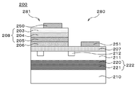
- FIG. 3 shows a second embodiment of the light emitting device of the present invention.
- the light emitting device 200 according to the second embodiment of the present invention is provided on the window layer / support substrate 210 and the window layer / support substrate 210, and the second conductivity type second semiconductor layer 205.
- a light emitting unit 208 including the active layer 204 and the first conductive type first semiconductor layer 203 in this order.
- a removal unit 280 from which at least the first semiconductor layer 203 and the active layer 204 have been removed and a non-removal unit 281 other than the removal unit 280 are provided.
- the first ohmic electrode 250 provided on the first semiconductor layer 203 of the non-removal part 281 and the second semiconductor layer 205 such as the buffer layer 206 and the current propagation layer 207 on the second semiconductor layer 205 of the removal part 280 or the buffer layer 206.
- a second ohmic electrode 251 provided on the second conductivity type semiconductor layer electrically connected to the first conductive layer.
- the window layer / supporting substrate 210 and the light emitting portion 208 are joined via the SiO 2 film 222.
- the window layer / support substrate 210 may be a transparent substrate made of, for example, GaP, GaAsP, sapphire, or the like.
- the SiO 2 film 222 includes a first SiO 2 film 220 provided on the light emitting unit 208 side, and a second SiO 2 film 221 provided on the window layer / supporting substrate 210 side.
- the two films 220 and the second SiO 2 film 221 are directly joined. That is, it is directly joined without using an adhesive. With such a structure, a light-emitting element in which peeling due to poor bonding is more reliably reduced is obtained.
- the first and second SiO 2 films 220 and 221 can have a thickness of 0.05 to 1.0 ⁇ m, for example.
- a first transparent conductive film layer 211 Between the first SiO 2 film 220 and the light emitting portion 208, a first transparent conductive film layer 211, a contact layer 212 formed on a part of the first transparent conductive film layer 211, a current propagation layer 207, And the buffer layer 206.
- the first transparent conductive film layer 211 can be made of an oxide containing at least one of Mg, Ni, Cu, Ga, In, and Sn, for example.
- the contact layer 212 is, for example, (Al x Ga 1-x ) y In 1-y P (0 ⁇ x ⁇ 1, 0 ⁇ y ⁇ 1) or Al z Ga 1-z As (0 ⁇ z ⁇ 1) or The thickness may be 0.005 to 0.1 ⁇ m made of GaAs w P 1-w (0 ⁇ w ⁇ 1).
- the current propagation layer 207 is made of, for example, Al z Ga 1-z As (0 ⁇ z ⁇ 1) or GaAs w P 1-w (0 ⁇ w ⁇ 1) and has a thickness of 0.5 to 5.0 ⁇ m. can do.
- the buffer layer 206 can be made of, for example, InGaP or AlInP and has a thickness of 0.1 to 1.0 ⁇ m.
- the light emitting unit 208 is made of, for example, (Al x Ga 1-x ) y In 1-y P (0 ⁇ x ⁇ 1, 0 ⁇ y ⁇ 1) or Al z Ga 1-z As (0 ⁇ z ⁇ 1).
- the second conductive type second semiconductor layer 205 having a thickness of 0.5 to 1.0 ⁇ m, the active layer 204 having a thickness of 0.1 to 1.0 ⁇ m, and the first conductive type having a thickness of 0.5 to 1.0 ⁇ m.
- the first semiconductor layer 203 may be included in this order.
- the active layer 204 has (Al x Ga 1-x ) y In 1-y P (0 ⁇ x ⁇ 1, 0.4 ⁇ y ⁇ 0.6) or Al z Ga 1-z As (0 ⁇ z ⁇ 0.45).
- AlGaInP When it is applied to visible light illumination, it is preferable to select AlGaInP, and when it is applied to infrared illumination, it is preferable to select AlGaAs or InGaAs.
- the design of the active layer 204 is not limited to the above materials because the wavelength can be adjusted to other than the wavelength resulting from the material composition by using a superlattice or the like.
- AlGaInP or AlGaAs is selected for the first semiconductor layer 203 and the second semiconductor layer 205, and the selection does not necessarily have to be the same material system as that of the active layer 204.
- the present invention is not limited to this, and at least the first semiconductor layer 203 is removed. It is sufficient that the layer 203 and the active layer 204 are removed.
- a substrate 201 is prepared as a starting substrate.
- the substrate 201 it is preferable to use a substrate 201 whose crystal axis is inclined in the [110] direction from the [001] direction.
- the substrate 201 GaAs or Ge can be preferably used. If the substrate 201 is selected from the above materials, the material of the active layer 204 to be described later can be epitaxially grown in a lattice-matched system, so that the quality of the active layer 204 can be easily improved, and the luminance and life characteristics can be improved. .
- a selective etching layer 202 for removing the substrate 201 may be formed on the substrate 201.
- the selective etching layer 202 has a layer structure of two or more layers, and preferably includes at least a first selective etching layer 202A in contact with the substrate 201 and a second selective etching layer 202B in contact with a first semiconductor layer 203 described later.
- the first selective etching layer 202A and the second selective etching layer 202B may be made of different materials or compositions.
- a step of sequentially forming a first conductive type first semiconductor layer 203, an active layer 204, and a second conductive type second semiconductor layer 205 using a lattice matching material with the substrate 201 by epitaxial growth is performed.
- the lattice constant is substantially the same as that of the substrate 201 on the substrate 201 (on the selective etching layer 202 when the selective etching layer 202 is provided) by, for example, the MOVPE method, the MBE method, or the CBE method.
- the epitaxial substrate 209 is produced by epitaxially growing the light emitting portion 208, the buffer layer 206, and the current propagation layer 207, which are composed of the first conductivity type first semiconductor layer 203, the active layer 204, the second conductivity type second semiconductor layer 205, in this order. can do.
- the current propagation layer 207 AlGaAs, GaAsP, or GaP can be suitably used.
- the buffer layer 206 is most preferably formed of InGaP or AlInP. Since there is a lattice mismatch between GaAs x P 1-x (x ⁇ 1) and the AlGaInP-based material or AlGaAs-based material, GaAs x P 1-x (x ⁇ 1) has high-density strain and Threading dislocation enters. The threading dislocation density can be adjusted by the composition x.
- a contact layer 212 is formed on a part of the current propagation layer 207, and the first transparent conductive film layer 211 is formed so as to cover the contact layer 212 and the current propagation layer 207. Can be formed.
- the first transparent conductive film layer 211 can be selected from oxides containing any one of In, Sn, Zn, Ga, and Cu, and can be formed by a sputtering method or the like.
- the film thickness of the first transparent conductive film layer 211 may be any film thickness that is greater than or equal to the contact layer 212 because a film thickness that provides flatness required for bonding may be selected in the bonding process described later. But you can choose.
- the first bonding substrate 230 can be formed by depositing the first SiO 2 film 220 on the first transparent conductive film layer 211.
- the first SiO 2 film 220 can be formed by optical CVD, sputtering, or PECVD.
- a second SiO 2 film 221 can be deposited on the window layer / support substrate 210 that is a transparent substrate to form a second bonding substrate 231.
- the second SiO 2 film 221 can be formed by optical CVD, sputtering, or PECVD.
- the window layer / support substrate 210 may be a transparent substrate made of, for example, GaP, GaAsP, sapphire, or the like.
- first bonded substrate 230 and the second bonded substrate 231 thus manufactured are washed with an alkaline aqueous solution such as NaOH. And it is preferable to perform the below-mentioned joining process after this washing
- a bonding step of bonding the window layer / supporting substrate 210 to the light emitting unit 208 is performed.
- the window layer / support substrate 210 is bonded to the light emitting unit 208 via the SiO 2 film 222.
- the bonding step it is preferable to directly bond the first SiO 2 film 220 formed on the light emitting unit 208 and the second SiO 2 film 221 formed on the window layer / supporting substrate 210. In this way, it is possible to manufacture a light emitting element in which peeling due to poor bonding is more reliably reduced.
- the first bonding substrate 230 and the second bonding substrate 231 are placed so that the first SiO 2 film 220 and the second SiO 2 film 221 face each other and do not come into contact with each other. Create a vacuum atmosphere. After making the vacuum atmosphere, the first SiO 2 film 220 and the second SiO 2 film 221 are brought into contact with each other, and a pressure of 5000 N and heat of 400 ° C. or more are applied to the first bonding substrate 230 and the second bonding substrate 231.
- the bonding substrate 240 can be formed by directly bonding and bonding.
- a step of removing the substrate 201 from the bonded substrate 240 is performed.
- the substrate 201 can be removed by etching.
- etching can be performed with a mixed solution of ammonia water and hydrogen peroxide water.
- etching with a mixed solution of ammonia water and hydrogen peroxide water can be selectively stopped.
- the first selective etching layer 202A can be removed.
- the second selective etching layer 202B can also be removed.
- hydrochloric acid or the like can be used for removing these.
- the first ohmic electrode 250 includes at least one material selected from Au, Ag, Al, Ni, Pd, Ge, Si, and Sn, and has a thickness of 200 nm or more. It can have.
- the first conductivity type is P-type
- the first ohmic electrode 250 can include at least one material selected from Au, Be, Mg, and Zn and have a thickness of 200 nm or more.
- a removal step of removing at least the first semiconductor layer 203 and the active layer 204 to form a removal portion 280 is performed.
- a pattern in which the first region 260 of the first semiconductor layer 203, the active layer 204, the second semiconductor layer 205, and the buffer layer 206 is notched is formed by etching by a dry method or a wet method.
- the removal part 280 and the non-removal part 281 other than the removal part 280 can be formed.
- FIG. 4G illustrates an example in which the buffer layer 206 is cut out, at least the first semiconductor layer 203 and the active layer 204 may be removed, and the second semiconductor layer 205 or the buffer layer 206 is exposed. Even if the etching is stopped, the same function is obtained.
- the first region 260 and a region other than the first region 260 may be covered with a dielectric film 270.
- a dielectric film 270 SiO 2 , SiN x or the like can be selected. After covering the dielectric film 270, a part of the first region 260 is etched to form the second region 261 in which the current propagation layer 207 is exposed.
- the second conductivity type semiconductor electrically connected to the second semiconductor layer 205 or the second semiconductor layer 205 such as the buffer layer 206 and the current propagation layer 207 of the removal portion 280.
- a step of forming a second ohmic electrode 251 on the layer is performed.
- the second ohmic electrode 251 is formed in a part of the second region 261 in the removal unit 280.
- FIG. 4I shows a case where the second ohmic electrode 251 is formed on the current propagation layer 207.
- the second ohmic electrode 251 includes at least one material selected from Au, Ag, Al, Ni, Pd, Ge, Si, and Sn and has a thickness of 100 nm or more. It can be.
- the second ohmic electrode 251 can include at least one material selected from Au, Be, Mg, and Zn and have a thickness of 100 nm or more.
- the window layer / support substrate 210 is bonded to the light emitting portion 208 via the SiO 2 film 222, a light emitting element in which peeling due to poor bonding is reduced can be manufactured.
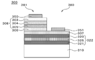
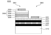
- FIG. 5 shows a third embodiment of the light emitting device of the present invention.
- the light emitting device 300 according to the third embodiment of the present invention is provided on the window layer / support substrate 310, the window layer / support substrate 310, and the second conductivity type second semiconductor layer 305.
- a removal unit 380 from which at least the first semiconductor layer 303 and the active layer 304 have been removed and a non-removal unit 381 other than the removal unit 380 are provided.
- the first ohmic electrode 350 provided on the first semiconductor layer 303 of the non-removal portion 381 and the second semiconductor layer 305 such as the second semiconductor layer 305 of the removal portion 380 or the buffer layer 306 and the current propagation layer 307.
- a second ohmic electrode 351 provided on the second conductivity type semiconductor layer electrically connected to the first and second semiconductor layers.
- the window layer / supporting substrate 310 and the light emitting portion 308 are bonded through the SiO 2 film 322.
- the window layer / support substrate 310 may be a transparent substrate made of, for example, GaP, GaAsP, sapphire, or the like.
- the SiO 2 film 322 includes a first SiO 2 film 320 provided on the light emitting unit 308 side and a second SiO 2 film 321 provided on the window layer / supporting substrate 310 side, and the first SiO 2 film 322 is provided.
- the two films 320 and the second SiO 2 film 321 are bonded via an adhesive 325. With such a structure, a light-emitting element in which peeling due to poor bonding is more reliably reduced is obtained.
- an adhesive made of BCB (benzocyclobutene) or epoxy can be used as the adhesive 325.
- the first and second SiO 2 films 320 and 321 can have a thickness of 0.05 to 1.0 ⁇ m, for example.
- a current propagation layer 307 and a buffer layer 306 may be provided between the first SiO 2 film 320 and the light emitting unit 308.
- the current propagation layer 307 is made of, for example, Al z Ga 1-z As (0 ⁇ z ⁇ 1) or GaAs w P 1-w (0 ⁇ w ⁇ 1) and has a thickness of 0.5 to 5.0 ⁇ m. can do.
- the buffer layer 306 can be made of, for example, InGaP or AlInP and has a thickness of 0.1 to 1.0 ⁇ m.
- the light emitting unit 308 is made of, for example, (Al x Ga 1-x ) y In 1-y P (0 ⁇ x ⁇ 1, 0 ⁇ y ⁇ 1) or Al z Ga 1-z As (0 ⁇ z ⁇ 1).
- the second conductivity type second semiconductor layer 305 having a thickness of 0.5 to 1.0 ⁇ m, the active layer 304 having a thickness of 0.1 to 1.0 ⁇ m, and the first conductivity type having a thickness of 0.5 to 1.0 ⁇ m.
- the first semiconductor layer 303 may be included in this order.
- the active layer 304 has (Al x Ga 1-x ) y In 1-y P (0 ⁇ x ⁇ 1, 0.4 ⁇ y ⁇ 0.6) or Al z Ga 1-z As (depending on the emission wavelength. 0 ⁇ z ⁇ 0.45).
- AlGaInP When it is applied to visible light illumination, it is preferable to select AlGaInP, and when it is applied to infrared illumination, it is preferable to select AlGaAs or InGaAs.
- the design of the active layer 304 is not limited to the above materials because the wavelength can be adjusted other than the wavelength resulting from the material composition by using a superlattice or the like.
- AlGaInP or AlGaAs is selected for the first semiconductor layer 303 and the second semiconductor layer 305, and the selection does not necessarily have to be the same material system as that of the active layer 304.
- the present invention is not limited to this, and at least the first semiconductor layer 303 is removed. It is sufficient that the layer 303 and the active layer 304 are removed.
- a substrate 301 is prepared as a starting substrate.
- the substrate 301 it is preferable to use a substrate 301 whose crystal axis is inclined in the [110] direction from the [001] direction.
- the substrate 301 GaAs or Ge can be preferably used. If the substrate 301 is selected from the above materials, the material of the active layer 304 to be described later can be epitaxially grown in a lattice matching system, so that the quality of the active layer 304 can be easily improved, and the luminance can be increased and the life characteristics can be improved. .
- a selective etching layer 302 for removing the substrate 301 may be formed on the substrate 301.
- the selective etching layer 302 has a layer structure of two or more layers, and preferably includes at least a first selective etching layer 302A in contact with the substrate 301 and a second selective etching layer 302B in contact with a first semiconductor layer 303 described later.
- the first selective etching layer 302A and the second selective etching layer 302B may be made of different materials or compositions.
- a process of forming the light emitting portion 308 by epitaxial growth of the first conductive type first semiconductor layer 303, the active layer 304, and the second conductive type second semiconductor layer 305 using a lattice matching material with the substrate 301 is performed. .
- the lattice constant is substantially the same as that of the substrate 301 by, for example, the MOVPE method, the MBE method, or the CBE method on the substrate 301 (on the selective etching layer 302 when the selective etching layer 302 is provided).
- the epitaxial substrate 309 is produced by epitaxially growing the light emitting portion 308, the buffer layer 306, and the current propagation layer 307 including the first conductivity type first semiconductor layer 303, the active layer 304, and the second conductivity type second semiconductor layer 305. can do.
- the current propagation layer 307 AlGaAs, GaAsP, or GaP can be preferably used.
- the buffer layer 306 is most preferably formed of InGaP or AlInP. Since there is a lattice mismatch between GaAs x P 1-x (x ⁇ 1) and the AlGaInP-based material or AlGaAs-based material, GaAs x P 1-x (x ⁇ 1) has high-density strain and Threading dislocation enters. The threading dislocation density can be adjusted by the composition x.
- a first SiO 2 film 320 is deposited on the current propagation layer 307, and an adhesive 325 (transparent adhesive layer) is formed on the first SiO 2 film 320.
- an adhesive 325 transparent adhesive layer
- the first SiO 2 film 320 can be formed by optical CVD, sputtering, or PECVD.
- the adhesive 325 can be selected from BCB (benzocyclobutene) or epoxy. It is preferable to select a material that can be formed by a dipping method or a spin coating method.
- volatilize the solvent by holding the first bonding substrate 330 on the hot plate in the range of 80 to 110 ° C. for 30 seconds or more. Since the solvent only needs to be volatilized, any of the above-mentioned conditions can be selected. However, it is preferable to select a holding time of 90 ° C. or more and 60 seconds or more.
- the second SiO 2 film 321 can be deposited on the window layer / support substrate 310 which is a transparent substrate, and the second bonding substrate 331 can be manufactured.
- the second SiO 2 film 321 can be formed by optical CVD, sputtering, or PECVD.
- the window layer / support substrate 310 can be a transparent substrate made of, for example, GaP, GaAsP, sapphire, or the like.
- FIGS. 6B and 6C the example in which the adhesive 325 is provided only on the first bonding substrate 330 is disclosed, but the same effect can be obtained even if the adhesive 325 is provided on the second bonding substrate 331. Needless to say.
- a bonding step of bonding the window layer / support substrate 310 to the light emitting unit 308 is performed.
- the window layer / support substrate 310 is bonded to the light emitting unit 308 through the SiO 2 film 322.
- the first SiO 2 film 320 formed on the light emitting portion 308 and the second SiO 2 film 321 formed on the window layer / supporting substrate 310 are bonded via an adhesive 325. In this way, it is possible to manufacture a light emitting element in which peeling due to poor bonding is more reliably reduced.
- the first bonding substrate 330 and the second bonding substrate 331 are placed so that the adhesive 325 and the second SiO 2 film 321 face each other and do not come into contact with each other, and a vacuum atmosphere of 30 Pa or less is obtained. .
- the adhesive 325 and the second SiO 2 film 321 are brought into contact with each other, and controlled so that the pressure is 5000 N and the temperature is between 100 to 200 ° C.
- the bonding substrate 340 can be formed by applying heat of at least ° C. and bonding the first bonding substrate 330 and the second bonding substrate 331 by pressure bonding.
- a step of removing the substrate 301 from the bonded substrate 340 is performed.
- the substrate 301 can be removed by etching.
- etching can be performed with a mixed solution of ammonia water and hydrogen peroxide water.
- etching using a mixed solution of ammonia water and hydrogen peroxide water can be selectively stopped.
- the first selective etching layer 302A can be removed.
- the second selective etching layer 302B can also be removed.
- hydrochloric acid or the like can be used for removing these.
- the first ohmic electrode 350 includes at least one material selected from Au, Ag, Al, Ni, Pd, Ge, Si, and Sn, and has a film thickness of 300 nm or more. It can have.
- the first conductivity type is P-type
- the first ohmic electrode 350 can include at least one material selected from Au, Be, Mg, and Zn and have a film thickness of 300 nm or more.
- a removal step of removing at least the first semiconductor layer 303 and the active layer 304 to form a removal portion 380 is performed.
- a pattern in which the first region 360 of the first semiconductor layer 303, the active layer 304, the second semiconductor layer 305, and the buffer layer 306 is cut out is formed by etching by a dry method or a wet method. Thereby, the removal part 380 and the non-removal part 381 other than this removal part 380 can be formed.
- FIG. 6G illustrates an example in which the buffer layer 306 is cut out, at least the first semiconductor layer 303 and the active layer 304 may be removed, and the second semiconductor layer 305 or the buffer layer 306 is exposed. Even if the etching is stopped, the same function is obtained.
- the first region 360 and the region other than the first region 360 may be covered with a dielectric film 370.
- the dielectric film 370 can be selected from SiO 2 , SiN x and the like. After covering the dielectric film 370, a part of the first region 360 is etched to form the second region 361 in which the current propagation layer 307 is exposed.
- the second conductivity type semiconductor electrically connected to the second semiconductor layer 305 or the second semiconductor layer 305 such as the buffer layer 306 and the current propagation layer 307 of the removal unit 380.
- a step of forming a second ohmic electrode 351 on the layer is performed.
- the second ohmic electrode 351 can be formed in a part of the second region 361 in the removal unit 380.
- FIG. 6I shows a case where the second ohmic electrode 351 is formed on the current propagation layer 307.
- the second ohmic electrode 351 includes at least one material selected from Au, Ag, Al, Ni, Pd, Ge, Si, and Sn and has a thickness of 300 nm or more. It can be.
- the second ohmic electrode 351 can include at least one material selected from Au, Be, Mg, and Zn and have a thickness of 300 nm or more.
- the window layer / support substrate 310 is bonded to the light emitting unit 308 through the SiO 2 film 322, a light emitting element in which peeling due to bonding failure is reduced can be manufactured.
- FIG. 7 shows a fourth embodiment of the light emitting device of the present invention.
- the light emitting device 400 according to the fourth embodiment of the present invention is provided on the window layer / support substrate 410 and the window layer / support substrate 410 and has the second conductivity type second semiconductor layer 405.
- a removal portion 480 from which at least the first semiconductor layer 403 and the active layer 404 have been removed and a non-removal portion 481 other than the removal portion 480 are provided.
- the first ohmic electrode 450 provided on the first semiconductor layer 403 of the non-removal part 481 and the second semiconductor layer 405 such as the second semiconductor layer 405 of the removal part 480 or the buffer layer 406 and the current propagation layer 407.
- a second ohmic electrode 451 provided on the second conductivity type semiconductor layer electrically connected to the first conductive layer.
- the window layer / supporting substrate 410 and the light emitting portion 408 are joined via the SiO 2 film 422.
- the window layer / support substrate 410 can be a transparent substrate made of, for example, GaP, GaAsP, sapphire, or the like.
- the SiO 2 film 422 includes a first SiO 2 film 420 provided on the light emitting unit 408 side and a second SiO 2 film 421 provided on the window layer / supporting substrate 410 side.
- the two films 420 and the second SiO 2 film 421 are bonded via an adhesive 425. With such a structure, a light-emitting element in which peeling due to poor bonding is more reliably reduced is obtained.
- an adhesive made of BCB (benzocyclobutene), epoxy, or the like can be used as the adhesive 425.
- the first and second SiO 2 films 420 and 421 can have a thickness of 0.05 to 1.0 ⁇ m, for example.
- a first transparent conductive film layer 411 Between the first SiO 2 film 420 and the light emitting portion 408, a first transparent conductive film layer 411, a contact layer 412 formed on a part of the first transparent conductive film layer 411, a current propagation layer 407, And a buffer layer 406.
- the first transparent conductive film layer 411 can be made of an oxide containing at least one of Mg, Ni, Cu, Ga, In, and Sn, for example.
- the contact layer 412 is formed of, for example, (Al x Ga 1-x ) y In 1-y P (0 ⁇ x ⁇ 1, 0 ⁇ y ⁇ 1), Al z Ga 1-z As (0 ⁇ z ⁇ 1) or The thickness may be 0.005 to 0.1 ⁇ m made of GaAs w P 1-w (0 ⁇ w ⁇ 1).
- the current propagation layer 407 is made of, for example, Al z Ga 1-z As (0 ⁇ z ⁇ 1) or GaAs w P 1-w (0 ⁇ w ⁇ 1) and has a thickness of 0.5 to 5.0 ⁇ m. can do.
- the buffer layer 406 can be made of, for example, InGaP or AlInP with a thickness of 0.1 to 1.0 ⁇ m.
- the light emitting unit 408 is made of, for example, (Al x Ga 1-x ) y In 1-y P (0 ⁇ x ⁇ 1, 0 ⁇ y ⁇ 1) or Al z Ga 1-z As (0 ⁇ z ⁇ 1).
- the second conductivity type second semiconductor layer 405 having a thickness of 0.5 to 1.0 ⁇ m, the active layer 404 having a thickness of 0.1 to 1.0 ⁇ m, and the first conductivity type having a thickness of 0.5 to 1.0 ⁇ m.
- the first semiconductor layer 403 may be included in this order.
- the active layer 404 has (Al x Ga 1-x ) y In 1-y P (0 ⁇ x ⁇ 1, 0.4 ⁇ y ⁇ 0.6) or Al z Ga 1-z As (depending on the emission wavelength. 0 ⁇ z ⁇ 0.45).
- AlGaInP When it is applied to visible light illumination, it is preferable to select AlGaInP, and when it is applied to infrared illumination, it is preferable to select AlGaAs or InGaAs.
- the design of the active layer 404 is not limited to the above materials because the wavelength can be adjusted to a wavelength other than the wavelength resulting from the material composition by using a superlattice or the like.
- AlGaInP or AlGaAs is selected for the first semiconductor layer 403 and the second semiconductor layer 405, and the selection is not necessarily the same material system as that of the active layer 404.
- the present invention is not limited to this, and at least the first semiconductor layer 403 is removed. It is sufficient that the layer 403 and the active layer 404 are removed.
- a substrate 401 is prepared as a starting substrate.
- the substrate 401 it is preferable to use a substrate 401 whose crystal axis is inclined in the [110] direction from the [001] direction.
- the substrate 401 GaAs or Ge can be preferably used. If the substrate 401 is selected from the above materials, the material of the active layer 404 to be described later can be epitaxially grown in a lattice matching system, so that the quality of the active layer 404 can be easily improved, and the luminance can be increased and the life characteristics can be improved. .
- a selective etching layer 402 for removing the substrate 401 may be formed on the substrate 401.
- the selective etching layer 402 has a layer structure of two or more layers, and preferably includes at least a first selective etching layer 402A in contact with the substrate 401 and a second selective etching layer 402B in contact with a first semiconductor layer 403 described later.
- the first selective etching layer 402A and the second selective etching layer 402B may be made of different materials or compositions.
- a step of forming the light emitting portion 408 by epitaxial growth of the first conductive type first semiconductor layer 403, the active layer 404, and the second conductive type second semiconductor layer 405 using a lattice matching material with the substrate 401 is performed.
- the lattice constant is substantially the same as that of the substrate 401 by, for example, the MOVPE method, the MBE method, or the CBE method on the substrate 401 (on the selective etching layer 402 when the selective etching layer 402 is provided).
- An epitaxial substrate 409 is produced by epitaxially growing the light emitting portion 408, the buffer layer 406, and the current propagation layer 407 including the first conductivity type first semiconductor layer 403, the active layer 404, and the second conductivity type second semiconductor layer 405. can do.
- the first semiconductor layer 403, the active layer 404, and the second semiconductor layer 405 having the simplest structure are exemplified by AlInGaP, which is the same material, but the first semiconductor layer 403 or the second semiconductor layer is exemplified.
- 405 generally includes a plurality of layers in each layer, and the second semiconductor layer 405 is not limited to a single layer.
- the first semiconductor layer 403 is composed of a layer having two or more types of Al composition, and has a layer having a high Al composition on the side close to the active layer 404 and a layer having a low Al composition on the side close to the substrate 401. be able to.
- the layer having a high Al composition on the side close to the active layer 404 is a functional layer having a function of a cladding layer, and does not mean a single composition or a single condition layer.
- the current propagation layer 407 AlGaAs, GaAsP, or GaP can be preferably used.
- the buffer layer 406 is most preferably formed of InGaP or AlInP. Since there is a lattice mismatch between GaAs x P 1-x (x ⁇ 1) and the AlGaInP-based material or AlGaAs-based material, GaAs x P 1-x (x ⁇ 1) has high-density strain and Threading dislocation enters. The threading dislocation density can be adjusted by the composition x.
- a contact layer 412 is formed on a part of the current propagation layer 407, and the first transparent conductive film layer 411 is formed so as to cover the contact layer 412 and the current propagation layer 407. Can be formed.
- the contact layer 412 includes at least one material selected from Au, Ag, Al, Ni, Pd, Ge, Si, and Sn and has a thickness of 100 nm or more. be able to.
- the contact layer 412 can include at least one material selected from Au, Be, Mg, and Zn and have a thickness of 0.005 to 0.1 ⁇ m. .
- a case where the second conductivity type is P-type and a structure of AuBe of 0.01 ⁇ m is selected as an electrode material is illustrated.
- the first transparent conductive film layer 411 can be selected from oxides containing any one of In, Sn, Zn, Ga, and Cu. In this embodiment, ITO is selected and deposited by sputtering. Illustrate.
- the film thickness of the first transparent conductive film layer 411 may be any film thickness that is equal to or greater than the contact layer 412 because a film thickness that provides flatness required for bonding may be selected in the bonding process described later. But you can choose.
- a first SiO 2 film 420 is deposited on the first transparent conductive film layer 411, an adhesive 425 (transparent adhesive layer) is formed on the first SiO 2 film 420, and the first bonding substrate 430 is formed. Can be produced.
- the first SiO 2 film 420 can be formed by optical CVD, sputtering, or PECVD.
- BCB or epoxy can be selected. It is preferable to select a material that can be formed by a dipping method or a spin coating method.
- the solvent by holding the first bonding substrate 430 in the range of 80 to 110 ° C. for 30 seconds or longer on the hot plate. Since the solvent only needs to be volatilized, any of the above-mentioned conditions can be selected. However, it is preferable to select a holding time of 90 ° C. or more and 60 seconds or more.
- a second SiO 2 film 421 can be deposited on the window layer / support substrate 410 which is a transparent substrate, so that a second bonded substrate 431 can be manufactured.
- the second SiO 2 film 421 can be formed by optical CVD, sputtering, or PECVD.
- the window layer / support substrate 410 can be a transparent substrate made of, for example, GaP, GaAsP, sapphire, or the like.
- a bonding step for bonding the window layer / support substrate 410 to the light emitting unit 408 is performed.
- the window layer / support substrate 410 is bonded to the light emitting unit 408 via the SiO 2 film 422.
- the first SiO 2 film 420 formed on the light emitting unit 408 and the second SiO 2 film 421 formed on the window layer / supporting substrate 410 are bonded via an adhesive 425. In this way, it is possible to manufacture a light emitting element in which peeling due to poor bonding is more reliably reduced.
- the first bonding substrate 430 and the second bonding substrate 431 are placed so that the adhesive 425 and the second SiO 2 film 421 face each other and do not come into contact with each other, and a vacuum atmosphere of 30 Pa or less is obtained. .
- the adhesive 425 and the second SiO 2 film 421 are brought into contact with each other, and controlled so that the pressure is 5000 N and the temperature is between 100 ° C. and 200 ° C.
- the bonded substrate 440 can be formed by applying heat of at least ° C. and bonding the first bonded substrate 430 and the second bonded substrate 431 by pressure bonding.
- a step of removing the substrate 401 from the bonded substrate 440 is performed.
- the substrate 401 can be removed by etching.
- etching can be performed with a mixed solution of ammonia water and hydrogen peroxide water.
- etching using a mixed solution of ammonia water and hydrogen peroxide water can be selectively stopped.
- the first selective etching layer 402A can be removed.
- the second selective etching layer 402B can also be removed.
- hydrochloric acid or the like can be used for removing these.
- the first ohmic electrode 450 includes at least one material selected from Au, Ag, Al, Ni, Pd, Ge, Si, and Sn and has a thickness of 400 nm or more. It can be.
- the first conductivity type is P-type
- the first ohmic electrode 450 can include at least one material selected from Au, Be, Mg, and Zn and have a thickness of 400 nm or more.
- a removal step of removing at least the first semiconductor layer 403 and the active layer 404 to form a removal portion 480 is performed.
- a pattern in which the first regions 460 of the first semiconductor layer 403, the active layer 404, the second semiconductor layer 405, and the buffer layer 406 are notched is formed by etching by a dry method or a wet method.
- the removal part 480 and the non-removal part 481 other than this removal part 480 can be formed.
- FIG. 8G illustrates an example in which the buffer layer 406 is cut out, at least the first semiconductor layer 403 and the active layer 404 may be removed, and the second semiconductor layer 405 or the buffer layer 406 is exposed.
- the region other than the first region 460 is represented as a flat surface, but is not limited to a flat surface, and the region other than the first region 460 may be a rough surface or an uneven surface. Needless to say.
- the first region 460 and a region other than the first region 460 may be covered with a dielectric film 470.
- the dielectric film 470 can be selected from SiO 2 , SiN x and the like. After covering the dielectric film 470, a part of the first region 460 can be etched to form the second region 461 in which the current propagation layer 407 is exposed.
- the second conductivity type semiconductor electrically connected to the second semiconductor layer 405 of the removal portion 480 or the second semiconductor layer 405 such as the buffer layer 406 and the current propagation layer 407.
- a step of forming a second ohmic electrode 451 on the layer is performed.
- the second ohmic electrode 451 can be formed in a part of the second region 461 in the removal portion 480.
- FIG. 8I shows a case where the second ohmic electrode 451 is formed on the current propagation layer 407.
- the second ohmic electrode 451 includes at least one material selected from Au, Ag, Al, Ni, Pd, Ge, Si, and Sn and has a thickness of 400 nm or more. It can be.
- the second ohmic electrode 451 may include at least one material selected from Au, Be, Mg, and Zn and have a thickness of 400 nm or more.
- the window layer / support substrate 410 is bonded to the light emitting portion 408 through the SiO 2 film 422, a light emitting element in which peeling due to bonding failure is reduced can be manufactured.
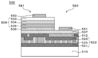
- FIG. 9 shows a fifth embodiment of the light emitting device of the present invention.
- the light emitting device 500 according to the fifth embodiment of the present invention is provided on the window layer / support substrate 510 and the window layer / support substrate 510, and the second conductivity type second semiconductor layer 505.
- a removal portion 580 from which at least the first semiconductor layer 503 and the active layer 504 have been removed and a non-removal portion 581 other than the removal portion 580 are provided.
- the first ohmic electrode 550 provided on the first semiconductor layer 503 of the non-removal portion 581 and the second semiconductor layer 505 such as the second semiconductor layer 505 of the removal portion 580 or the buffer layer 506 and the current propagation layer 507. And a second ohmic electrode 551 provided on a second conductivity type semiconductor layer electrically connected to the first conductive layer. Further, the window layer / supporting substrate 510 and the light emitting portion 508 are bonded via the SiO 2 film 522.
- the window layer / supporting substrate 510 can be a transparent substrate made of, for example, GaP, GaAsP, sapphire, or the like.
- the SiO 2 film 522 includes a first SiO 2 film 520 provided on the light emitting unit 508 side and a second SiO 2 film 521 provided on the window layer / supporting substrate 510 side.
- the two films 520 and the second SiO 2 film 521 are bonded via an adhesive 525. With such a structure, a light-emitting element in which peeling due to poor bonding is more reliably reduced is obtained.
- an adhesive made of BCB (benzocyclobutene) or epoxy can be used as the adhesive 525.
- a metal pattern layer 512 formed on a part of the upper surface of the first SiO 2 film 520, a current propagation layer 507, and a buffer layer 506 are provided. Can be.
- the first and second SiO 2 films 520 and 521 can have a thickness of 0.05 to 1.0 ⁇ m, for example.
- the current propagation layer 507 is made of, for example, Al z Ga 1-z As (0 ⁇ z ⁇ 1) or GaAs w P 1-w (0 ⁇ w ⁇ 1) and has a thickness of 0.5 to 5.0 ⁇ m. can do.
- the buffer layer 506 can be made of, for example, InGaP or AlInP and has a thickness of 0.1 to 1.0 ⁇ m.
- the light emitting unit 508 is formed from, for example, (Al x Ga 1-x ) y In 1-y P (0 ⁇ x ⁇ 1, 0 ⁇ y ⁇ 1) or Al z Ga 1-z As (0 ⁇ z ⁇ 1).
- the second conductivity type second semiconductor layer 505 having a thickness of 0.5 to 1.0 ⁇ m, the active layer 504 having a thickness of 0.1 to 1.0 ⁇ m, and the first conductivity type having a thickness of 0.5 to 1.0 ⁇ m.
- the first semiconductor layer 503 can be included in this order.
- the active layer 504 has (Al x Ga 1-x ) y In 1-y P (0 ⁇ x ⁇ 1, 0.4 ⁇ y ⁇ 0.6) or Al z Ga 1-z As (depending on the emission wavelength. 0 ⁇ z ⁇ 0.45).
- AlGaInP When it is applied to visible light illumination, it is preferable to select AlGaInP, and when it is applied to infrared illumination, it is preferable to select AlGaAs or InGaAs.
- the design of the active layer 504 is not limited to the above materials because the wavelength can be adjusted other than the wavelength resulting from the material composition by using a superlattice or the like.
- AlGaInP or AlGaAs is selected for the first semiconductor layer 503 and the second semiconductor layer 505, and the selection is not necessarily the same material system as that of the active layer 504.
- FIG. 9 shows a case where the first semiconductor layer 503, the active layer 504, the second semiconductor layer 505, and the buffer layer 506 are removed.
- the present invention is not limited to this, and at least the first semiconductor layer 503 is removed. It is sufficient that the layer 503 and the active layer 504 are removed.
- a substrate 501 is prepared as a starting substrate as shown in FIG.
- the substrate 501 it is preferable to use a substrate 501 whose crystal axis is inclined in the [110] direction from the [001] direction.
- the substrate 501 GaAs or Ge can be preferably used. If the substrate 501 is selected from the above materials, the material of the active layer 504, which will be described later, can be epitaxially grown in a lattice-matched system, so that the quality of the active layer 504 can be easily improved, and luminance can be improved and lifetime characteristics can be improved. .
- a selective etching layer 502 for removing the substrate 501 may be formed on the substrate 501.
- the selective etching layer 502 has a layer structure of two or more layers, and preferably includes at least a first selective etching layer 502A in contact with the substrate 501 and a second selective etching layer 502B in contact with a first semiconductor layer 503 described later.
- the first selective etching layer 502A and the second selective etching layer 502B may be made of different materials or compositions.
- a step of forming a light emitting portion 508 by epitaxial growth of a first conductive type first semiconductor layer 503, an active layer 504, and a second conductive type second semiconductor layer 505 using a lattice matching material with the substrate 501 is performed.
- the lattice constant is substantially the same as that of the substrate 501 by, for example, the MOVPE method, the MBE method, or the CBE method on the substrate 501 (on the selective etching layer 502 when the selective etching layer 502 is provided).
- the epitaxial substrate 509 is produced by epitaxially growing the light emitting portion 508, the buffer layer 506, and the current propagation layer 507 including the first conductivity type first semiconductor layer 503, the active layer 504, and the second conductivity type second semiconductor layer 505 in this order. can do.
- the first semiconductor layer 503 or the second semiconductor layer is exemplified.
- each layer generally includes a plurality of layers, and the second semiconductor layer 505 is not limited to a single layer.
- the first semiconductor layer 503 is composed of a layer having two or more types of Al composition, and has a layer having a high Al composition on the side close to the active layer 504 and a layer having a low Al composition on the side close to the substrate 501. be able to.
- the layer having a high Al composition on the side close to the active layer 504 is a functional layer having a function of a cladding layer, and does not mean a single composition or a single condition layer.
- the current propagation layer 507 AlGaAs, GaAsP, or GaP can be suitably used.
- the buffer layer 506 is most preferably formed of InGaP or AlInP. Since there is a lattice mismatch between GaAs x P 1-x (x ⁇ 1) and the AlGaInP-based material or AlGaAs-based material, GaAs x P 1-x (x ⁇ 1) has high-density strain and Threading dislocation enters. The threading dislocation density can be adjusted by the composition x.
- a metal pattern layer 512 is formed on part of the current propagation layer 507, and the first SiO 2 film is formed so as to cover the metal pattern layer 512 and the current propagation layer 507.
- 520 can be deposited.
- the first SiO 2 film 520 can be formed by optical CVD, sputtering, or PECVD.
- an adhesive 525 transparent adhesive layer is formed on the first SiO 2 film 520, and the first bonded substrate 530 can be manufactured.
- the adhesive 525 can be selected from BCB or epoxy. It is preferable to select a material that can be formed by a dipping method or a spin coating method.
- the solvent by holding the first bonding substrate 530 in the range of 80 to 110 ° C. for 30 seconds or longer on the hot plate. Since the solvent only needs to be volatilized, any of the above-mentioned conditions can be selected. However, it is preferable to select a holding time of 90 ° C. or more and 60 seconds or more.
- a second SiO 2 film 521 can be deposited on the window layer / support substrate 510 which is a transparent substrate to produce a second bonding substrate 531.
- the second SiO 2 film 521 can be formed by optical CVD, sputtering, or PECVD.
- the window layer / supporting substrate 510 can be a transparent substrate made of, for example, GaP, GaAsP, sapphire, or the like.
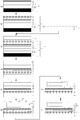
- FIGS. 10B and 10C the example in which the adhesive 525 is provided only on the first bonding substrate 530 is disclosed, but the same effect can be obtained even if the adhesive 525 is provided on the second bonding substrate 531. .
- a bonding step of bonding the window layer / supporting substrate 510 to the light emitting portion 508 is performed.
- the window layer / support substrate 510 is bonded to the light emitting unit 508 via the SiO 2 film 522.
- the first SiO 2 film 520 formed on the light emitting unit 508 and the second SiO 2 film 521 formed on the window layer / supporting substrate 510 are bonded via an adhesive 525. In this way, it is possible to manufacture a light emitting element in which peeling due to poor bonding is more reliably reduced.
- the first bonding substrate 530 and the second bonding substrate 531 are placed so that the adhesive 525 and the second SiO 2 film 521 face each other and do not come into contact with each other, and a vacuum atmosphere of 30 Pa or less is obtained. .
- the adhesive 525 and the second SiO 2 film 521 are brought into contact with each other, and controlled so that the pressure is 5000 N and the temperature is between 100 ° C. and 200 ° C.
- the bonding substrate 540 can be formed by applying heat at a temperature equal to or higher than 0 ° C. and bonding the first bonding substrate 530 and the second bonding substrate 531 by pressure bonding.
- a step of removing the substrate 501 from the bonding substrate 540 is performed.
- the substrate 501 can be removed by etching.
- etching can be performed with a mixed solution of ammonia water and hydrogen peroxide water.
- etching using a mixed solution of ammonia water and hydrogen peroxide water can be selectively stopped.
- the first selective etching layer 502A can be removed.
- the second selective etching layer 502B can also be removed.
- hydrochloric acid or the like can be used for removing these.
- the first ohmic electrode 550 includes at least one material selected from Au, Ag, Al, Ni, Pd, Ge, Si, and Sn and has a thickness of 500 nm or more. It can be.
- the first conductivity type is P-type
- the first ohmic electrode 550 can include at least one material selected from Au, Be, Mg, and Zn and have a thickness of 500 nm or more.
- a removal step of removing at least the first semiconductor layer 503 and the active layer 504 to form a removal portion 580 is performed.
- a pattern in which the first regions 560 of the first semiconductor layer 503, the active layer 504, the second semiconductor layer 505, and the buffer layer 506 are notched is formed by etching by a dry method or a wet method.
- the removal part 580 and the non-removal part 581 other than the removal part 580 can be formed.
- FIG. 10G illustrates an example in which the buffer layer 506 is cut out, but at least the first semiconductor layer 503 and the active layer 504 may be removed, and the second semiconductor layer 505 or the buffer layer 506 is exposed. Even if the etching is stopped, the same function is obtained.
- the first region 560 and a region other than the first region 560 may be covered with a dielectric film 570.
- the dielectric film 570 can be selected from SiO 2 , SiN x and the like. After covering the dielectric film 570, a part of the first region 560 can be etched to form the second region 561 in which the current propagation layer 507 is exposed.
- the second conductivity type semiconductor electrically connected to the second semiconductor layer 505 or the second semiconductor layer 505 such as the buffer layer 506 and the current propagation layer 507 of the removal portion 580.
- a step of forming a second ohmic electrode 551 on the layer is performed.
- the second ohmic electrode 551 can be formed in a part of the second region 561 in the removal portion 580.
- FIG. 10I shows a case where the second ohmic electrode 551 is formed on the current propagation layer 507.
- the second ohmic electrode 551 includes at least one material selected from Au, Ag, Al, Ni, Pd, Ge, Si, and Sn and has a thickness of 500 nm or more. It can be.
- the second ohmic electrode 551 can include at least one material selected from Au, Be, Mg, and Zn and have a thickness of 500 nm or more.
- the window layer / support substrate 510 is bonded to the light emitting portion 508 via the SiO 2 film 522, a light emitting element in which peeling due to poor bonding is reduced can be manufactured.
- Example 1 10,000 light emitting devices 100 according to the first embodiment of the present invention as shown in FIG. 1 were manufactured by the method for manufacturing a light emitting device according to the first embodiment of the present invention.
- the light emitting device 100 manufactured in Example 1 has the same thickness as that of the second SiO 2 film 121 having a thickness of 0.5 ⁇ m on the window layer / supporting substrate 110 which is a transparent substrate made of GaP.
- a current propagation layer 107 made of AlGaAs with a thickness of 1.0 ⁇ m a buffer layer 106 made of AlInP with a thickness of 0.5 ⁇ m, and a thickness of 1.0 ⁇ m made of AlGaInP.
- a light emitting section 108 is formed which includes the p-type second semiconductor layer 105, the active layer 104 having a thickness of 0.5 ⁇ m, and the n-type first semiconductor layer 103 having a thickness of 1.0 ⁇ m in this order.
- the removal part 180 from which the active layer 104, the first conductivity type first semiconductor layer 103, the second conductivity type second semiconductor layer 105, and the buffer layer 106 are removed, and the non-removal part 181 other than the removal part 180, have.
- first ohmic electrode 150 made of AuGeNi is formed on the surface of the first semiconductor layer 103 of the non-removed portion 181, and a 500 nm thick made of AuBe on the surface of the current propagation layer 107 of the removed portion 180. And a two-ohmic electrode 151.
- Example 2 With the method for manufacturing a light emitting device according to the second embodiment of the present invention, 10,000 light emitting devices 200 according to the second embodiment of the present invention as shown in FIG. 3 were manufactured.
- the light emitting device 200 manufactured in Example 2 is on the first transparent conductive film layer 211 and the first transparent conductive film layer 211 between the first SiO 2 film 220 and the current propagation layer 207.
- the structure was the same as that of Example 1 except that a contact layer 212 made of AlGaInP and having a thickness of 0.05 ⁇ m was partially formed.
- Example 3 The light emitting device manufacturing method according to the third embodiment of the present invention manufactured 10,000 light emitting devices 300 according to the third embodiment of the present invention as shown in FIG.
- the light-emitting element 300 manufactured in Example 3 is the same as Example except that the first and second SiO 2 films 320 and 321 are bonded via an adhesive 325 made of BCB (benzocyclobutene). The same structure as that of No. 1 was adopted.
- BCB benzocyclobutene
- Example 4 The light emitting device manufacturing method according to the fourth embodiment of the present invention manufactured 10,000 light emitting devices 400 according to the fourth embodiment of the present invention as shown in FIG.
- the light emitting device 400 manufactured in Example 4 is the same as Example except that the first and second SiO 2 films 420 and 421 are bonded via an adhesive 425 made of BCB (benzocyclobutene).
- the structure was the same as 2.
- Example 5 The light emitting device manufacturing method according to the fifth embodiment of the present invention manufactured 10,000 light emitting devices 500 according to the fifth embodiment of the present invention as shown in FIG.
- the light emitting device 500 manufactured in Example 5 has the same structure as that of Example 3 except that the metal pattern layer 512 is formed on a part of the upper surface of the first SiO 2 film 520.
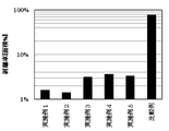
- the peel rate of the light emitting element manufactured in the comparative example was 78%.
- the peel rates of the light emitting devices manufactured in Examples 1 to 5 were all 4% or less. As described above, in the light-emitting elements manufactured in Examples 1 to 5, it was possible to reduce peeling due to bonding failure that occurred during bonding, as compared with the light-emitting elements manufactured in Comparative Examples.
- the present invention is not limited to the above embodiment.
- the above-described embodiment is an exemplification, and the present invention has any configuration that has substantially the same configuration as the technical idea described in the claims of the present invention and that exhibits the same effects. Are included in the technical scope.
Landscapes
- Led Devices (AREA)
Abstract
本発明は、窓層兼支持基板と、該窓層兼支持基板上に設けられ、第二導電型の第二半導体層と活性層と第一導電型の第一半導体層とをこの順に含む発光部とを有する発光素子において、少なくとも前記第一半導体層と前記活性層が除去された除去部と、該除去部以外の非除去部と、該非除去部の前記第一半導体層上に設けられた第一オーミック電極と、前記除去部の前記第二半導体層上または前記第二半導体層に電気的に接続した第二導電型の半導体層上に設けられた第二オーミック電極とを有し、前記窓層兼支持基板と前記発光部とがSiO2膜を介して接合されたものであることを特徴とする発光素子である。これにより、接合時に生じる接合不良による剥離が低減された発光素子及びその製造方法が提供される。
Description
本発明は、発光素子及びその製造方法に関する。
チップオンボード(COB)などの製品は、LED素子からの放熱性に優れ、照明等の用途において、採用されるLEDチップ実装方法である。COBなどにLEDを実装する場合、チップを直接ボードに接合するフリップ実装が必須である。フリップ実装を実現するためには、発光素子の一方の面に極性の異なる通電用パッドを設けたフリップチップを作製する必要がある。また、通電用パッドが設けられた面の反対側の面は光取り出し機能を有する材料で構成する必要がある。
黄色~赤色LEDでフリップチップを作製する場合、発光層にはAlGaInP系の材料が用いられる。AlGaInP系材料はバルク結晶が存在せず、エピタキシャル法でLED部は形成されるため、出発基板はAlGaInPとは異なる材料が選択される。出発基板はGaAsやGeが選択される場合が多く、これらの基板は可視光に対して光吸収の特性を有するため、フリップチップを作製する場合、出発基板は除去される。しかし、発光層を形成するエピタキシャル層は極薄膜のため、出発基板除去後に自立することができない。したがって、発光層に発光波長に対して略透明で窓層としての機能を有し、自立させるために十分の厚さを有する支持基板としての機能を有する材料・構成の窓層兼支持基板を、出発基板と置換する必要がある。
このような窓層兼支持基板の機能を有する置換材料として、GaP、GaAsP、サファイアなどが選択される。前記いずれの材料を選択しても、AlGaInP系材料と異なる材料であるため、格子定数、熱膨張係数やヤング率などの機械的特性はAlGaInP系材料とは異なる。
このような技術として、特許文献1には窓層兼支持基板としてGaPを結晶成長と直接接合により形成する方法が開示されている。この技術では直接接合するGaP基板の大きさによって発光素子用ウェハの大きさが決まり、ウェハを大口径化することが難しい問題がある。このため、この技術では小さい発光素子には向いても、大きな発光素子には向かない。
また、特許文献2には窓層兼支持基板としてGaPを結晶成長して形成する方法が開示されている。この技術によればGaP基板を接合しないため、接合基板の大きさの制約を受けない。しかし、GaPとAlGaInP発光層部には大きな格子不整が存在し、反りが発生する。ウェハを大口径化すると反りが大きくなるため、大きいウェハを使用するとデバイスプロセスが難しくなる問題がある。このため、この技術では小さい発光素子には向いても、大きな発光素子には向かない。
また、特許文献3には表面が荒れた発光層を透明接着層で接合する技術が開示されている。この技術では、接合自体は可能だが、接着剤と発光層及び被接合ウェハとの密着性が悪く、接合不良部の発生が回避できない。
このように、基板(出発基板)が発光素子から発する光を吸収する材料である発光素子ウェハを窓層兼支持基板(透明基板)に接合後、基板を除去する工程を有する発光素子及びその製造方法において、従来の方法では接合不良が生じやすく、歩留まりを上げることが困難であった。
本発明は前述のような問題に鑑みてなされたもので、接合時に生じる接合不良による剥離が低減された発光素子及びその製造方法を提供することを目的とする。
上記目的を達成するために、本発明によれば、窓層兼支持基板と、該窓層兼支持基板上に設けられ、第二導電型の第二半導体層と活性層と第一導電型の第一半導体層とをこの順に含む発光部とを有する発光素子において、
少なくとも前記第一半導体層と前記活性層が除去された除去部と、該除去部以外の非除去部と、該非除去部の前記第一半導体層上に設けられた第一オーミック電極と、前記除去部の前記第二半導体層上または前記第二半導体層に電気的に接続した第二導電型の半導体層上に設けられた第二オーミック電極とを有し、
前記窓層兼支持基板と前記発光部とがSiO2膜を介して接合されたものであることを特徴とする発光素子を提供する。
少なくとも前記第一半導体層と前記活性層が除去された除去部と、該除去部以外の非除去部と、該非除去部の前記第一半導体層上に設けられた第一オーミック電極と、前記除去部の前記第二半導体層上または前記第二半導体層に電気的に接続した第二導電型の半導体層上に設けられた第二オーミック電極とを有し、
前記窓層兼支持基板と前記発光部とがSiO2膜を介して接合されたものであることを特徴とする発光素子を提供する。
このように、窓層兼支持基板と発光部とがSiO2膜を介して接合されたものであるので、接合不良による剥離が低減された発光素子となる。
このとき、前記SiO2膜は、前記発光部側に設けられた第一のSiO2膜と、前記窓層兼支持基板側に設けられた第二のSiO2膜とを有し、前記第一のSiO2膜と第二のSiO2膜とが直接接合されたものであることが好ましい。
このようなものであれば、接合不良による剥離がより確実に低減された発光素子となる。
またこのとき、前記SiO2膜は、前記発光部側に設けられた第一のSiO2膜と、前記窓層兼支持基板側に設けられた第二のSiO2膜とを有し、前記第一のSiO2膜と第二のSiO2膜とが接着剤を介して接合されたものであることが好ましい。
このようなものであれば、接合不良による剥離がより確実に低減された発光素子となる。
また、本発明によれば基板上に、該基板と格子整合系の材料で少なくとも第一半導体層、活性層、第二半導体層を順次エピタキシャル成長により発光部を形成する工程と、窓層兼支持基板を前記発光部と接合する接合工程と、前記基板を除去する工程と、前記第一半導体層表面に第一オーミック電極を形成する工程と、少なくとも前記第一半導体層と前記活性層を除去して除去部を形成する除去工程と、前記除去部の前記第二半導体層または前記第二半導体層に電気的に接続した第二導電型の半導体層上に第二オーミック電極を形成する工程からなる発光素子の製造方法において、
前記接合工程において、SiO2膜を介して前記窓層兼支持基板を前記発光部と接合することを特徴とする発光素子の製造方法を提供する。
前記接合工程において、SiO2膜を介して前記窓層兼支持基板を前記発光部と接合することを特徴とする発光素子の製造方法を提供する。
このように、SiO2膜を介して前記窓層兼支持基板を前記発光部と接合するので、接合不良による剥離が低減された発光素子を製造することができる。
このとき、前記接合工程において、前記発光部上に形成した第一のSiO2膜と、前記窓層兼支持基板上に形成した第二のSiO2膜とを直接接合することが好ましい。
このようにすれば、接合不良による剥離がより確実に低減された発光素子を製造することができる。
またこのとき、前記接合工程において、前記発光部上に形成した第一のSiO2膜と、前記窓層兼支持基板上に形成した第二のSiO2膜とを接着剤を介して接合することが好ましい。
このようにすれば、接合不良による剥離がより確実に低減された発光素子を製造することができる。
本発明の発光素子及び発光素子の製造方法であれば、接合不良による剥離が低減された発光素子を実現できる。
以下、本発明について実施の形態を説明するが、本発明はこれに限定されるものではない。
上記したように、基板が発光素子から発する光を吸収する材料である発光素子ウェハを窓層兼支持基板に接合後、基板を除去する工程を有する発光素子及びその製造方法において、従来の方法では接合不良が生じやすく、歩留まりを上げることが困難であった。
上記したように、基板が発光素子から発する光を吸収する材料である発光素子ウェハを窓層兼支持基板に接合後、基板を除去する工程を有する発光素子及びその製造方法において、従来の方法では接合不良が生じやすく、歩留まりを上げることが困難であった。
そこで、本発明者らはこのような問題を解決すべく鋭意検討を重ねた。その結果、窓層兼支持基板と発光部とがSiO2膜を介して接合されたものであれば、接合不良による剥離が低減された発光素子とすることができることに想到した。そして、これらを実施するための最良の形態について精査し、本発明を完成させた。
(第一の実施形態)
図1に本発明の発光素子の第一の実施形態を示した。図1に示すように、本発明の第一の実施形態における発光素子100は、窓層兼支持基板110と、窓層兼支持基板110上に設けられ、第二導電型の第二半導体層105と活性層104と第一導電型の第一半導体層103とをこの順に含む発光部108とを有している。また、少なくとも第一半導体層103及び活性層104が除去された除去部180と、該除去部180以外の非除去部181とを有している。そして、非除去部181の第一半導体層103上に設けられた第一オーミック電極150と、除去部180の第二半導体層105上または緩衝層106及び電流伝播層107等の第二半導体層105に電気的に接続した第二導電型の半導体層上に設けられた第二オーミック電極151とを有している。また、窓層兼支持基板110と発光部108とがSiO2膜122を介して接合されたものである。
図1に本発明の発光素子の第一の実施形態を示した。図1に示すように、本発明の第一の実施形態における発光素子100は、窓層兼支持基板110と、窓層兼支持基板110上に設けられ、第二導電型の第二半導体層105と活性層104と第一導電型の第一半導体層103とをこの順に含む発光部108とを有している。また、少なくとも第一半導体層103及び活性層104が除去された除去部180と、該除去部180以外の非除去部181とを有している。そして、非除去部181の第一半導体層103上に設けられた第一オーミック電極150と、除去部180の第二半導体層105上または緩衝層106及び電流伝播層107等の第二半導体層105に電気的に接続した第二導電型の半導体層上に設けられた第二オーミック電極151とを有している。また、窓層兼支持基板110と発光部108とがSiO2膜122を介して接合されたものである。
窓層兼支持基板110は、例えば、GaP、GaAsP、サファイア等からなる透明基板とすることができる。
SiO2膜122は、発光部108側に設けられた第一のSiO2膜120と、窓層兼支持基板110側に設けられた第二のSiO2膜121とを有し、第一のSiO2膜120と第二のSiO2膜121とが直接接合されたものである。すなわち、接着剤を介さずに直接接合されたものである。このようなものであれば、接合不良による剥離がより確実に低減された発光素子となる。
第一及び第二のSiO2膜120、121は、例えば、厚さ0.05~1.0μmのものとすることができる。
第一のSiO2膜120と発光部108との間に、電流伝播層107と緩衝層106を有するものとすることができる。
電流伝播層107は、例えば、AlzGa1-zAs(0≦z≦1)またはGaAswP1-w(0≦w≦1)からなる厚さ0.5~5.0μmのものとすることができる。緩衝層106は、例えば、InGaPまたはAlInPからなる厚さ0.1~1.0μmのものとすることができる。
発光部108は、例えば、(AlxGa1-x)yIn1-yP(0≦x≦1、0≦y≦1)あるいはAlzGa1-zAs(0≦z≦1)からなる厚さ0.5~1.0μmの第二導電型の第二半導体層105、厚さ0.1~1.0μmの活性層104、厚さ0.5~1.0μmの第一導電型の第一半導体層103とをこの順に含むものとすることができる。
活性層104は、発光波長に応じて(AlxGa1-x)yIn1-yP(0≦x≦1、0.4≦y≦0.6)またはAlzGa1-zAs(0≦z≦0.45)で形成されたものとすることができる。可視光照明に適用する場合、AlGaInPを選択するのが好適であり、赤外照明に適用する場合、AlGaAsあるいはInGaAsを選択するのが好適である。ただし、活性層104の設計に関しては、超格子等の利用により波長は材料組成に起因する波長以外に調整可能であるため、上記の材料に限られない。
第一半導体層103、第二半導体層105はAlGaInPもしくはAlGaAsが選択され、その選択は活性層104と必ずしも同一の材料系でなくともよい。
図1の除去部180では、第一半導体層103、活性層104、第二半導体層105及び緩衝層106が除去された場合を示したが、本発明はこれに限定されず、少なくとも第一半導体層103及び活性層104が除去されたものであればよい。
このような発光素子100であれば、窓層兼支持基板110と発光部108とがSiO2膜122を介して接合されたものであるので、接合不良による剥離が低減されたものとなる。
次に、本発明の第一の実施形態における発光素子の製造方法について、図2を用いて説明する。
最初に、図2(a)に示すように、出発基板として基板101を準備する。基板101として、結晶軸が[001]方向より[110]方向に傾斜した基板101を用いることが好ましい。また、基板101としては、GaAsまたはGeを好適に用いることができる。基板101を上記材料から選択すれば、後述する活性層104の材料を格子整合系でエピタキシャル成長を行うことができるため、活性層104の品質を向上させやすく、輝度上昇や寿命特性の向上が得られる。
次に、基板101の上に、基板101の除去用の選択エッチング層102を形成してもよい。選択エッチング層102は二層以上の層構造からなり、基板101に接する第一の選択エッチング層102A、後述する第一半導体層103に接する第二の選択エッチング層102Bを少なくとも有することが好ましい。第一の選択エッチング層102Aと第二の選択エッチング層102Bは異なる材料あるいは組成から構成しても良い。
次に、基板101と格子整合系の材料で第一導電型の第一半導体層103、活性層104、第二導電型の第二半導体層105を順次エピタキシャル成長により発光部108を形成する工程を行う。
このとき、具体的には、基板101上(選択エッチング層102を設けた場合には、選択エッチング層102上)に、例えばMOVPE法(有機金属気相成長法)やMBE法(分子線エピタキシー法)、CBE法(化学線エピタキシー法)により、第一導電型の第一半導体層103、活性層104、第二導電型の第二半導体層105から成る発光部108、緩衝層106、電流伝播層107をこの順にエピタキシャル成長したエピタキシャル基板109を作製することができる。
電流伝播層107としては、AlGaAsまたはGaAsPまたはGaPを好適に用いることができる。電流伝播層107をGaAsxP1-x(0≦x<1)で形成した場合、緩衝層106はInGaPあるいはAlInPで形成するのが最も好適である。GaAsxP1-x(x≠1)と、AlGaInP系材料またはAlGaAs系材料との間には格子不整が存在するため、GaAsxP1-x(x≠1)には高密度のひずみや貫通転位が入る。貫通転位密度は組成xにより調整可能である。
次に、図2(b)に示すように、電流伝播層107上に第一のSiO2膜120を堆積し、第一接合基板130を作製することができる。第一のSiO2膜120は、光CVD、スパッタ法、PECVD法にて形成することができる。
図2(c)に示すように、透明基板である窓層兼支持基板110上に第二のSiO2膜121を堆積し、第二接合基板131を作製することができる。第二のSiO2膜121は、光CVD、スパッタ法、PECVD法にて形成することができる。窓層兼支持基板110は、例えば、GaP、GaAsP、サファイア等からなる透明基板とすることができる。
このようにして作製した第一接合基板130と第二接合基板131を、NaOH等のアルカリ水溶液にて洗浄することが好ましい。そして、この洗浄後に、後述の接合工程を行うことが好ましい。
次に、図2(d)に示すように、窓層兼支持基板110を発光部108と接合する接合工程を行う。このとき、SiO2膜122を介して窓層兼支持基板110を発光部108と接合する。
そして、接合工程において、発光部108上に形成した第一のSiO2膜120と、窓層兼支持基板110上に形成した第二のSiO2膜121とを直接接合することが好ましい。このようにすれば、接合不良による剥離がより確実に低減された発光素子を製造することができる。
具体的には、例えば、第一接合基板130と第二接合基板131を、第一のSiO2膜120と第二のSiO2膜121を対向させ、かつ接触しないように設置し、10Pa以下の真空雰囲気にする。真空雰囲気とした後、第一のSiO2膜120と第二のSiO2膜121を接触させ、かつ、5000Nの圧力と400℃以上の熱を加えて第一接合基板130と第二接合基板131を圧着して直接接合することによって、接合基板140を形成することができる。
次に、図2(e)に示すように、接合基板140より基板101を除去する工程を行う。基板101の除去は、エッチングにより行うことができる。エッチングに際しては、アンモニア水と過酸化水素水の混合液にてエッチングを行うことができる。第一の選択エッチング層102Aを基板101と異なる材料にしておくことで、アンモニア水と過酸化水素水の混合液によるエッチングを選択的に停止させることができる。
基板101除去後、第一の選択エッチング層102Aを除去することができる。同様に、第二の選択エッチング層102Bも除去することができる。これらの除去には例えば塩酸等を用いることができる。
次に、図2(f)に示すように、第一半導体層103表面に第一オーミック電極150を形成する工程を行う。このとき、第一導電型がN型の場合、第一オーミック電極150は、Au、Ag、Al、Ni、Pd、Ge、Si、Snから少なくとも一種類以上の材料を含み、100nm以上の膜厚を有するものとすることができる。第一導電型がP型の場合、第一オーミック電極150は、Au、Be、Mg、Znから少なくとも一種類以上の材料を含み、100nm以上の膜厚を有するものとすることができる。
次に、図2(g)に示すように、少なくとも第一半導体層103と活性層104を除去して除去部180を形成する除去工程を行う。具体的には、例えば、ドライ法あるいはウェット法によるエッチングによって第一半導体層103、活性層104、第二半導体層105、緩衝層106の第一の領域160を切り欠いたパターンを形成する。これにより、除去部180と、該除去部180以外の非除去部181を形成することができる。図2(g)では緩衝層106まで切り欠いた例を図示しているが、少なくとも第一半導体層103と活性層104を除去すればよく、第二半導体層105あるいは緩衝層106が露出した状態でエッチングを止めても同様の機能を有する。
次に、図2(h)に示すように、第一の領域160及び第一の領域160以外の領域を被覆するように誘電体膜170で被覆してもよい。誘電体膜170は、SiO2、SiNx等が選択可能である。誘電体膜170を被覆後、第一の領域160の一部をエッチングし、電流伝播層107を露出させた第二の領域161を形成することができる。
次に、図2(i)に示すように、除去部180の第二半導体層105または緩衝層106及び電流伝播層107等の第二半導体層105に電気的に接続した第二導電型の半導体層上に第二オーミック電極151を形成する工程を行う。
具体的には、除去部180における第二の領域161の一部に第二オーミック電極151を形成することができる。図2(i)では、第二オーミック電極151を電流伝播層107上に形成した場合を示している。
第二導電型がN型の場合、第二オーミック電極151は、Au、Ag、Al、Ni、Pd、Ge、Si、Snから少なくとも一種類以上の材料を含み、100nm以上の膜厚を有するものとすることができる。第二導電型がP型の場合、第二オーミック電極151は、Au、Be、Mg、Znから少なくとも一種類以上の材料を含み、100nm以上の膜厚を有するものとすることができる。
次に、ステルスダイシング法、あるいはブレードダイシング法によって個別ダイスに分割し、発光素子とすることができる。
このように、SiO2膜122を介して窓層兼支持基板110を発光部108と接合するので、接合不良による剥離が低減された発光素子を製造することができる。
(第二の実施形態)
図3に本発明の発光素子の第二の実施形態を示した。図3に示すように、本発明の第二の実施形態における発光素子200は、窓層兼支持基板210と、窓層兼支持基板210上に設けられ、第二導電型の第二半導体層205と活性層204と第一導電型の第一半導体層203とをこの順に含む発光部208とを有している。また、少なくとも第一半導体層203及び活性層204が除去された除去部280と、該除去部280以外の非除去部281とを有している。そして、非除去部281の第一半導体層203上に設けられた第一オーミック電極250と、除去部280の第二半導体層205上または緩衝層206及び電流伝播層207等の第二半導体層205に電気的に接続した第二導電型の半導体層上に設けられた第二オーミック電極251とを有している。また、窓層兼支持基板210と発光部208とがSiO2膜222を介して接合されたものである。
図3に本発明の発光素子の第二の実施形態を示した。図3に示すように、本発明の第二の実施形態における発光素子200は、窓層兼支持基板210と、窓層兼支持基板210上に設けられ、第二導電型の第二半導体層205と活性層204と第一導電型の第一半導体層203とをこの順に含む発光部208とを有している。また、少なくとも第一半導体層203及び活性層204が除去された除去部280と、該除去部280以外の非除去部281とを有している。そして、非除去部281の第一半導体層203上に設けられた第一オーミック電極250と、除去部280の第二半導体層205上または緩衝層206及び電流伝播層207等の第二半導体層205に電気的に接続した第二導電型の半導体層上に設けられた第二オーミック電極251とを有している。また、窓層兼支持基板210と発光部208とがSiO2膜222を介して接合されたものである。
窓層兼支持基板210は、例えば、GaP、GaAsP、サファイア等からなる透明基板とすることができる。
SiO2膜222は、発光部208側に設けられた第一のSiO2膜220と、窓層兼支持基板210側に設けられた第二のSiO2膜221とを有し、第一のSiO2膜220と第二のSiO2膜221とが直接接合されたものである。すなわち、接着剤を介さずに直接接合されたものである。このようなものであれば、接合不良による剥離がより確実に低減された発光素子となる。
第一及び第二のSiO2膜220、221は、例えば、厚さ0.05~1.0μmのものとすることができる。
第一のSiO2膜220と発光部208との間に、第一透明導電膜層211と、第一透明導電膜層211上の一部に形成されたコンタクト層212と、電流伝播層207と、緩衝層206とを有するものとすることができる。
第一透明導電膜層211は、例えば、Mg、Ni、Cu、Ga、In、Snのうちいずれか一種類以上を含む酸化物から構成されるものとすることができる。
コンタクト層212は、例えば、(AlxGa1-x)yIn1-yP(0≦x≦1、0≦y≦1)あるいはAlzGa1-zAs(0≦z≦1)あるいはGaAswP1-w(0≦w≦1)からなる厚さ0.005~0.1μmのものとすることができる。
電流伝播層207は、例えば、AlzGa1-zAs(0≦z≦1)またはGaAswP1-w(0≦w≦1)からなる厚さ0.5~5.0μmのものとすることができる。緩衝層206は、例えば、InGaPまたはAlInPからなる厚さ0.1~1.0μmのものとすることができる。発光部208は、例えば、(AlxGa1-x)yIn1-yP(0≦x≦1、0≦y≦1)あるいはAlzGa1-zAs(0≦z≦1)からなる厚さ0.5~1.0μmの第二導電型の第二半導体層205、厚さ0.1~1.0μmの活性層204、厚さ0.5~1.0μmの第一導電型の第一半導体層203とをこの順に含むものとすることができる。
活性層204は発光波長に応じて(AlxGa1-x)yIn1-yP(0≦x≦1、0.4≦y≦0.6)またはAlzGa1-zAs(0≦z≦0.45)で形成されたものとすることができる。可視光照明に適用する場合、AlGaInPを選択するのが好適であり、赤外照明に適用する場合、AlGaAsあるいはInGaAsを選択するのが好適である。ただし、活性層204の設計に関しては、超格子等の利用により波長は材料組成に起因する波長以外に調整可能であるため、上記の材料に限られない。
第一半導体層203、第二半導体層205はAlGaInPもしくはAlGaAsが選択され、その選択は活性層204と必ずしも同一の材料系でなくともよい。
図3の除去部280では、第一半導体層203、活性層204、第二半導体層205及び緩衝層206が除去された場合を示したが、本発明はこれに限定されず、少なくとも第一半導体層203及び活性層204が除去されたものであればよい。
このような発光素子200であれば、窓層兼支持基板210と発光部208とがSiO2膜222を介して接合されたものであるので、接合不良による剥離が低減されたものとなる。
次に、本発明の第二の実施形態における発光素子の製造方法について、図4を用いて説明する。
最初に、図4(a)に示すように、出発基板として基板201を準備する。基板201として、結晶軸が[001]方向より[110]方向に傾斜した基板201を用いることが好ましい。また、基板201としては、GaAsまたはGeを好適に用いることができる。基板201を上記材料から選択すれば、後述する活性層204の材料を格子整合系でエピタキシャル成長を行うことができるため、活性層204の品質を向上させやすく、輝度上昇や寿命特性の向上が得られる。
次に、基板201の上に、基板201の除去用の選択エッチング層202を形成してもよい。選択エッチング層202は二層以上の層構造からなり、基板201に接する第一の選択エッチング層202A、後述する第一半導体層203に接する第二の選択エッチング層202Bを少なくとも有することが好ましい。第一の選択エッチング層202Aと第二の選択エッチング層202Bは異なる材料あるいは組成から構成しても良い。
次に、基板201と格子整合系の材料で第一導電型の第一半導体層203、活性層204、第二導電型の第二半導体層205を順次エピタキシャル成長により発光部208を形成する工程を行う。
このとき、具体的には、基板201上(選択エッチング層202を設けた場合には、選択エッチング層202上)に、例えばMOVPE法やMBE法、CBE法により、基板201と格子定数が略同一の第一導電型の第一半導体層203、活性層204、第二導電型の第二半導体層205から成る発光部208、緩衝層206、電流伝播層207をこの順にエピタキシャル成長したエピタキシャル基板209を作製することができる。
電流伝播層207としては、AlGaAsまたはGaAsPまたはGaPを好適に用いることができる。電流伝播層207をGaAsxP1-x(0≦x<1)で形成した場合、緩衝層206はInGaPあるいはAlInPで形成するのが最も好適である。GaAsxP1-x(x≠1)と、AlGaInP系材料またはAlGaAs系材料との間には格子不整が存在するため、GaAsxP1-x(x≠1)には高密度のひずみや貫通転位が入る。貫通転位密度は組成xにより調整可能である。
次に、図4(b)に示すように、電流伝播層207上の一部にコンタクト層212を形成し、コンタクト層212及び電流伝播層207を被覆するように第一透明導電膜層211を形成することができる。
第一透明導電膜層211は、In、Sn、Zn、Ga、Cuのいずれか一つを含む酸化物から選択可能であり、スパッタ法等により形成することができる。第一透明導電膜層211の膜厚は、後述する接合工程において、接合に要する平坦度が有られる膜厚を選択すればよいため、コンタクト層212以上の膜厚があればどのような膜厚でも選択可能である。
次に、第一透明導電膜層211上に第一のSiO2膜220を堆積して第一接合基板230を形成することができる。第一のSiO2膜220は、光CVD、スパッタ法、PECVD法にて形成することが可能である。
次に、図4(c)に示すように、透明基板である窓層兼支持基板210上に第二のSiO2膜221を堆積し、第二接合基板231を形成することができる。第二のSiO2膜221は、光CVD、スパッタ法、PECVD法にて形成することが可能である。窓層兼支持基板210は、例えば、GaP、GaAsP、サファイア等からなる透明基板とすることができる。
このようにして作製した第一接合基板230と第二接合基板231を、NaOH等のアルカリ水溶液にて洗浄することが好ましい。そして、この洗浄後に、後述の接合工程を行うことが好ましい。
次に、図4(d)に示すように、窓層兼支持基板210を発光部208と接合する接合工程を行う。このとき、SiO2膜222を介して窓層兼支持基板210を発光部208と接合する。
そして、接合工程において、発光部208上に形成した第一のSiO2膜220と、窓層兼支持基板210上に形成した第二のSiO2膜221とを直接接合することが好ましい。このようにすれば、接合不良による剥離がより確実に低減された発光素子を製造することができる。
具体的には、例えば、第一接合基板230と第二接合基板231を、第一のSiO2膜220と第二のSiO2膜221を対向させ、かつ接触しないように設置し、20Pa以下の真空雰囲気にする。真空雰囲気とした後、第一のSiO2膜220と第二のSiO2膜221を接触させ、かつ、5000Nの圧力と400℃以上の熱を加えて第一接合基板230と第二接合基板231を圧着して直接接合することによって、接合基板240を形成することができる。
次に、図4(e)に示すように接合基板240より基板201を除去する工程を行う。基板201の除去は、エッチングにより行うことができる。エッチングに際しては、アンモニア水と過酸化水素水の混合液にてエッチングを行うことができる。第一の選択エッチング層202Aを基板201と異なる材料にしておくことで、アンモニア水と過酸化水素水の混合液によるエッチングを選択的に停止させることができる。
基板201除去後、第一の選択エッチング層202Aを除去することができる。同様に、第二の選択エッチング層202Bも除去することができる。これらの除去には例えば塩酸等を用いることができる。
次に、図4(f)に示すように、第一半導体層203表面に第一オーミック電極250を形成する工程を行う。このとき、第一導電型がN型の場合、第一オーミック電極250は、Au、Ag、Al、Ni、Pd、Ge、Si、Snから少なくとも一種類以上の材料を含み、200nm以上の膜厚を有するものとすることができる。第一導電型がP型の場合、第一オーミック電極250は、Au、Be、Mg、Znから少なくとも一種類以上の材料を含み、200nm以上の膜厚を有するものとすることができる。
次に、図4(g)に示すように、少なくとも第一半導体層203と活性層204を除去して除去部280を形成する除去工程を行う。具体的には、例えば、ドライ法あるいはウェット法によるエッチングによって第一半導体層203、活性層204、第二半導体層205、緩衝層206の第一の領域260を切り欠いたパターンを形成する。これにより、除去部280と、該除去部280以外の非除去部281を形成することができる。図4(g)では緩衝層206まで切り欠いた例を図示しているが、少なくとも第一半導体層203と活性層204を除去すればよく、第二半導体層205あるいは緩衝層206が露出した状態でエッチングを止めても同様の機能を有する。
次に、図4(h)に示すように、第一の領域260及び第一の領域260以外の領域を被覆するように誘電体膜270で被覆してもよい。誘電体膜270は、SiO2、SiNx等が選択可能である。誘電体膜270を被覆後、第一の領域260の一部をエッチングし、電流伝播層207を露出させた第二の領域261を形成することができる。
次に、図4(i)に示すように、除去部280の第二半導体層205または緩衝層206及び電流伝播層207等の第二半導体層205に電気的に接続した第二導電型の半導体層上に第二オーミック電極251を形成する工程を行う。
具体的には、除去部280における第二の領域261の一部に第二オーミック電極251を形成する。図4(i)では、第二オーミック電極251を電流伝播層207上に形成した場合を示している。
第二導電型がN型の場合、第二オーミック電極251は、Au、Ag、Al、Ni、Pd、Ge、Si、Snから少なくとも一種類以上の材料を含み、100nm以上の膜厚を有するものとすることができる。第二導電型がP型の場合、第二オーミック電極251は、Au、Be、Mg、Znから少なくとも一種類以上の材料を含み、100nm以上の膜厚を有するものとすることができる。
次に、ステルスダイシング法、あるいはブレードダイシング法によって個別ダイスに分割し、発光素子とするとすることができる。
このように、SiO2膜222を介して窓層兼支持基板210を発光部208と接合するので、接合不良による剥離が低減された発光素子を製造することができる。
(第三の実施形態)
図5に本発明の発光素子の第三の実施形態を示した。図5に示すように、本発明の第三の実施形態における発光素子300は、窓層兼支持基板310と、窓層兼支持基板310上に設けられ、第二導電型の第二半導体層305と活性層304と第一導電型の第一半導体層303とをこの順に含む発光部308とを有している。また、少なくとも第一半導体層303及び活性層304が除去された除去部380と、該除去部380以外の非除去部381とを有している。そして、非除去部381の第一半導体層303上に設けられた第一オーミック電極350と、除去部380の第二半導体層305上または緩衝層306及び電流伝播層307等の第二半導体層305に電気的に接続した第二導電型の半導体層上に設けられた第二オーミック電極351とを有している。また、窓層兼支持基板310と発光部308とがSiO2膜322を介して接合されたものである。
図5に本発明の発光素子の第三の実施形態を示した。図5に示すように、本発明の第三の実施形態における発光素子300は、窓層兼支持基板310と、窓層兼支持基板310上に設けられ、第二導電型の第二半導体層305と活性層304と第一導電型の第一半導体層303とをこの順に含む発光部308とを有している。また、少なくとも第一半導体層303及び活性層304が除去された除去部380と、該除去部380以外の非除去部381とを有している。そして、非除去部381の第一半導体層303上に設けられた第一オーミック電極350と、除去部380の第二半導体層305上または緩衝層306及び電流伝播層307等の第二半導体層305に電気的に接続した第二導電型の半導体層上に設けられた第二オーミック電極351とを有している。また、窓層兼支持基板310と発光部308とがSiO2膜322を介して接合されたものである。
窓層兼支持基板310は、例えば、GaP、GaAsP、サファイア等からなる透明基板とすることができる。
SiO2膜322は、発光部308側に設けられた第一のSiO2膜320と、窓層兼支持基板310側に設けられた第二のSiO2膜321とを有し、第一のSiO2膜320と第二のSiO2膜321とが接着剤325を介して接合されたものである。このようなものであれば、接合不良による剥離がより確実に低減された発光素子となる。
接着剤325は、BCB(ベンゾシクロブテン)あるいはエポキシ等からなる接着剤等を用いることができる。
第一及び第二のSiO2膜320、321は、例えば、厚さ0.05~1.0μmのものとすることができる。
第一のSiO2膜320と発光部308との間に、電流伝播層307及び緩衝層306を有するものとすることができる。
電流伝播層307は、例えば、AlzGa1-zAs(0≦z≦1)またはGaAswP1-w(0≦w≦1)からなる厚さ0.5~5.0μmのものとすることができる。緩衝層306は、例えば、InGaPまたはAlInPからなる厚さ0.1~1.0μmのものとすることができる。
発光部308は、例えば、(AlxGa1-x)yIn1-yP(0≦x≦1、0≦y≦1)あるいはAlzGa1-zAs(0≦z≦1)からなる厚さ0.5~1.0μmの第二導電型の第二半導体層305、厚さ0.1~1.0μmの活性層304、厚さ0.5~1.0μmの第一導電型の第一半導体層303とをこの順に含むものとすることができる。
活性層304は、発光波長に応じて(AlxGa1-x)yIn1-yP(0≦x≦1、0.4≦y≦0.6)またはAlzGa1-zAs(0≦z≦0.45)で形成されたものとすることができる。可視光照明に適用する場合、AlGaInPを選択するのが好適であり、赤外照明に適用する場合、AlGaAsあるいはInGaAsを選択するのが好適である。ただし、活性層304の設計に関しては、超格子等の利用により波長は材料組成に起因する波長以外に調整可能であるため、上記の材料に限られない。
第一半導体層303、第二半導体層305はAlGaInPもしくはAlGaAsが選択され、その選択は活性層304と必ずしも同一の材料系でなくともよい。
図5の除去部380では、第一半導体層303、活性層304、第二半導体層305及び緩衝層306が除去された場合を示したが、本発明はこれに限定されず、少なくとも第一半導体層303及び活性層304が除去されたものであればよい。
このような発光素子300であれば、窓層兼支持基板310と発光部308とがSiO2膜322を介して接合されたものであるので、接合不良による剥離が低減されたものとなる。
次に、本発明の第三の実施形態における発光素子の製造方法について、図6を用いて説明する。
最初に、図6(a)に示すように、出発基板として基板301を準備する。基板301として、結晶軸が[001]方向より[110]方向に傾斜した基板301を用いることが好ましい。また、基板301としては、GaAsまたはGeを好適に用いることができる。基板301を上記材料から選択すれば、後述する活性層304の材料を格子整合系でエピタキシャル成長を行うことができるため、活性層304の品質を向上させやすく、輝度上昇や寿命特性の向上が得られる。
次に、基板301上に、基板301の除去用の選択エッチング層302を形成してもよい。選択エッチング層302は二層以上の層構造からなり、基板301に接する第一の選択エッチング層302A、後述する第一半導体層303に接する第二の選択エッチング層302Bを少なくとも有することが好ましい。第一の選択エッチング層302Aと第二の選択エッチング層302Bは異なる材料あるいは組成から構成しても良い。
次に、基板301と格子整合系の材料で第一導電型の第一半導体層303、活性層304、第二導電型の第二半導体層305を順次エピタキシャル成長により発光部308を形成する工程を行う。
このとき、具体的には、基板301上(選択エッチング層302を設けた場合には、選択エッチング層302上)に、例えばMOVPE法やMBE法、CBE法により、基板301と格子定数が略同一の第一導電型の第一半導体層303、活性層304、第二導電型の第二半導体層305から成る発光部308、緩衝層306、電流伝播層307をこの順にエピタキシャル成長したエピタキシャル基板309を作製することができる。
電流伝播層307としては、AlGaAsまたはGaAsPまたはGaPを好適に用いることができる。電流伝播層307をGaAsxP1-x(0≦x<1)で形成した場合、緩衝層306はInGaPあるいはAlInPで形成するのが最も好適である。GaAsxP1-x(x≠1)と、AlGaInP系材料またはAlGaAs系材料との間には格子不整が存在するため、GaAsxP1-x(x≠1)には高密度のひずみや貫通転位が入る。貫通転位密度は組成xにより調整可能である。
次に、図6(b)に示すように、電流伝播層307上に第一のSiO2膜320を堆積し、この第一のSiO2膜320上に接着剤325(透明接着層)を形成し、第一接合基板330を作製することができる。
第一のSiO2膜320は、光CVD、スパッタ法、PECVD法にて形成することが可能である。
接着剤325は、BCB(ベンゾシクロブテン)あるいはエポキシ等が選択可能である。形成方法はディップ法あるいはスピンコート法により形成可能な材料を選択することが好適である。
次に、ホットプレート上に、第一接合基板330を80~110℃の範囲で30秒以上保持して溶剤を揮発させることが好ましい。溶剤が揮発すればよいため、前述のどの条件でも選択可能だが、温度90℃以上、60秒以上の保持時間を選択することが好適である。
図6(c)に示すように、透明基板である窓層兼支持基板310上に第二のSiO2膜321を堆積し、第二接合基板331を作製することができる。第二のSiO2膜321は、光CVD、スパッタ法、PECVD法にて形成することが可能である。窓層兼支持基板310は、例えば、GaP、GaAsP、サファイア等からなる透明基板とすることができる。
図6(b)、(c)においては、第一接合基板330のみに接着剤325を設けた例を開示したが、第二接合基板331に接着剤325を設けても同様の効果が得られることは言うまでも無い。
次に、図6(d)に示すように、窓層兼支持基板310を発光部308と接合する接合工程を行う。このとき、SiO2膜322を介して窓層兼支持基板310を発光部308と接合する。
そして、接合工程において、発光部308上に形成した第一のSiO2膜320と、窓層兼支持基板310上に形成した第二のSiO2膜321とを接着剤325を介して接合する。このようにすれば、接合不良による剥離がより確実に低減された発光素子を製造することができる。
具体的には、例えば、第一接合基板330と第二接合基板331を、接着剤325と第二のSiO2膜321を対向させ、かつ接触しないように設置し、30Pa以下の真空雰囲気にする。真空雰囲気とした後、接着剤325と第二のSiO2膜321を接触させ、かつ、5000Nの圧力と100~200℃の間の温度になるように制御して5分以上保持した後、300℃以上の熱を加えて第一接合基板330と第二接合基板331を圧着して接合することによって、接合基板340を形成することができる。
次に、図6(e)に示すように、接合基板340より基板301を除去する工程を行う。基板301の除去は、エッチングにより行うことができる。エッチングに際しては、アンモニア水と過酸化水素水の混合液にてエッチングを行うことができる。第一の選択エッチング層302Aを基板301と異なる材料にしておくことで、アンモニア水と過酸化水素水の混合液によるエッチングを選択的に停止させることができる。
基板301除去後、第一の選択エッチング層302Aを除去することができる。同様に、第二の選択エッチング層302Bも除去することができる。これらの除去には例えば塩酸等を用いることができる。
次に、図6(f)に示すように、第一半導体層303表面に第一オーミック電極350を形成する工程を行う。このとき、第一導電型がN型の場合、第一オーミック電極350は、Au、Ag、Al、Ni、Pd、Ge、Si、Snから少なくとも一種類以上の材料を含み、300nm以上の膜厚を有するものとすることができる。第一導電型がP型の場合、第一オーミック電極350は、Au、Be、Mg、Znから少なくとも一種類以上の材料を含み、300nm以上の膜厚を有するものとすることができる。
次に、図6(g)に示すように、少なくとも第一半導体層303と活性層304を除去して除去部380を形成する除去工程を行う。
具体的には、例えば、ドライ法あるいはウェット法によるエッチングによって第一半導体層303、活性層304、第二半導体層305、緩衝層306の第一の領域360を切り欠いたパターンを形成する。これにより、除去部380と、該除去部380以外の非除去部381を形成することができる。図6(g)では緩衝層306まで切り欠いた例を図示しているが、少なくとも第一半導体層303と活性層304を除去すればよく、第二半導体層305あるいは緩衝層306が露出した状態でエッチングを止めても同様の機能を有する。
次に、図6(h)に示すように、第一の領域360及び第一の領域360以外の領域を被覆するように誘電体膜370で被覆してもよい。誘電体膜370は、SiO2、SiNx等が選択可能である。誘電体膜370を被覆後、第一の領域360の一部をエッチングし、電流伝播層307を露出させた第二の領域361を形成することができる。
次に、図6(i)に示すように、除去部380の第二半導体層305または緩衝層306及び電流伝播層307等の第二半導体層305に電気的に接続した第二導電型の半導体層上に第二オーミック電極351を形成する工程を行う。
具体的には、除去部380における第二の領域361の一部に第二オーミック電極351を形成することができる。図6(i)では、第二オーミック電極351を電流伝播層307上に形成した場合を示している。
第二導電型がN型の場合、第二オーミック電極351は、Au、Ag、Al、Ni、Pd、Ge、Si、Snから少なくとも一種類以上の材料を含み、300nm以上の膜厚を有するものとすることができる。第二導電型がP型の場合、第二オーミック電極351は、Au、Be、Mg、Znから少なくとも一種類以上の材料を含み、300nm以上の膜厚を有するものとすることができる。
次に、ステルスダイシング法、あるいはブレードダイシング法によって個別ダイスに分割し、発光素子とすることができる。
このように、SiO2膜322を介して窓層兼支持基板310を発光部308と接合するので、接合不良による剥離が低減された発光素子を製造することができる。
(第四の実施形態)
図7に本発明の発光素子の第四の実施形態を示した。図7に示すように、本発明の第四の実施形態における発光素子400は、窓層兼支持基板410と、窓層兼支持基板410上に設けられ、第二導電型の第二半導体層405と活性層404と第一導電型の第一半導体層403とをこの順に含む発光部408とを有している。また、少なくとも第一半導体層403及び活性層404が除去された除去部480と、該除去部480以外の非除去部481とを有している。そして、非除去部481の第一半導体層403上に設けられた第一オーミック電極450と、除去部480の第二半導体層405上または緩衝層406及び電流伝播層407等の第二半導体層405に電気的に接続した第二導電型の半導体層上に設けられた第二オーミック電極451とを有している。また、窓層兼支持基板410と発光部408とがSiO2膜422を介して接合されたものである。
図7に本発明の発光素子の第四の実施形態を示した。図7に示すように、本発明の第四の実施形態における発光素子400は、窓層兼支持基板410と、窓層兼支持基板410上に設けられ、第二導電型の第二半導体層405と活性層404と第一導電型の第一半導体層403とをこの順に含む発光部408とを有している。また、少なくとも第一半導体層403及び活性層404が除去された除去部480と、該除去部480以外の非除去部481とを有している。そして、非除去部481の第一半導体層403上に設けられた第一オーミック電極450と、除去部480の第二半導体層405上または緩衝層406及び電流伝播層407等の第二半導体層405に電気的に接続した第二導電型の半導体層上に設けられた第二オーミック電極451とを有している。また、窓層兼支持基板410と発光部408とがSiO2膜422を介して接合されたものである。
窓層兼支持基板410は、例えば、GaP、GaAsP、サファイア等からなる透明基板とすることができる。
SiO2膜422は、発光部408側に設けられた第一のSiO2膜420と、窓層兼支持基板410側に設けられた第二のSiO2膜421とを有し、第一のSiO2膜420と第二のSiO2膜421とが接着剤425を介して接合されたものである。このようなものであれば、接合不良による剥離がより確実に低減された発光素子となる。
接着剤425は、BCB(ベンゾシクロブテン)あるいはエポキシ等からなる接着剤等を用いることができる。
第一及び第二のSiO2膜420、421は、例えば、厚さ0.05~1.0μmのものとすることができる。
第一のSiO2膜420と発光部408との間に、第一透明導電膜層411と、第一透明導電膜層411上の一部に形成されたコンタクト層412と、電流伝播層407と、緩衝層406とを有するものとすることができる。
第一透明導電膜層411は、例えば、Mg、Ni、Cu、Ga、In、Snのうちいずれか一種類以上を含む酸化物から構成されるものとすることができる。
コンタクト層412は、例えば、(AlxGa1-x)yIn1-yP(0≦x≦1、0≦y≦1)あるいはAlzGa1-zAs(0≦z≦1)あるいはGaAswP1-w(0≦w≦1)からなる厚さ0.005~0.1μmのものとすることができる。
電流伝播層407は、例えば、AlzGa1-zAs(0≦z≦1)またはGaAswP1-w(0≦w≦1)からなる厚さ0.5~5.0μmのものとすることができる。緩衝層406は、例えば、InGaPまたはAlInPからなる厚さ0.1~1.0μmのものとすることができる。
発光部408は、例えば、(AlxGa1-x)yIn1-yP(0≦x≦1、0≦y≦1)あるいはAlzGa1-zAs(0≦z≦1)からなる厚さ0.5~1.0μmの第二導電型の第二半導体層405、厚さ0.1~1.0μmの活性層404、厚さ0.5~1.0μmの第一導電型の第一半導体層403とをこの順に含むものとすることができる。
活性層404は、発光波長に応じて(AlxGa1-x)yIn1-yP(0≦x≦1、0.4≦y≦0.6)またはAlzGa1-zAs(0≦z≦0.45)で形成されたものとすることができる。可視光照明に適用する場合、AlGaInPを選択するのが好適であり、赤外照明に適用する場合、AlGaAsあるいはInGaAsを選択するのが好適である。ただし、活性層404の設計に関しては、超格子等の利用により波長は材料組成に起因する波長以外に調整可能であるため、上記の材料に限られない。
第一半導体層403、第二半導体層405はAlGaInPもしくはAlGaAsが選択され、その選択は活性層404と必ずしも同一の材料系でなくともよい。
図7の除去部480では、第一半導体層403、活性層404、第二半導体層405及び緩衝層406が除去された場合を示したが、本発明はこれに限定されず、少なくとも第一半導体層403及び活性層404が除去されたものであればよい。
このような発光素子400であれば、窓層兼支持基板410と発光部408とがSiO2膜422を介して接合されたものであるので、接合不良による剥離が低減されたものとなる。
次に、本発明の第四の実施形態における発光素子の製造方法について、図8を用いて説明する。
最初に、図8(a)に示すように、出発基板として基板401を準備する。基板401として、結晶軸が[001]方向より[110]方向に傾斜した基板401を用いることが好ましい。また、基板401としては、GaAsまたはGeを好適に用いることができる。基板401を上記材料から選択すれば、後述する活性層404の材料を格子整合系でエピタキシャル成長を行うことができるため、活性層404の品質を向上させやすく、輝度上昇や寿命特性の向上が得られる。
次に、基板401の上に、基板401の除去用の選択エッチング層402を形成してもよい。選択エッチング層402は二層以上の層構造からなり、基板401に接する第一の選択エッチング層402A、後述する第一半導体層403に接する第二の選択エッチング層402Bを少なくとも有することが好ましい。第一の選択エッチング層402Aと第二の選択エッチング層402Bは異なる材料あるいは組成から構成しても良い。
次に、基板401と格子整合系の材料で第一導電型の第一半導体層403、活性層404、第二導電型の第二半導体層405を順次エピタキシャル成長により発光部408を形成する工程を行う。
このとき、具体的には、基板401上(選択エッチング層402を設けた場合には、選択エッチング層402上)に、例えばMOVPE法やMBE法、CBE法により、基板401と格子定数が略同一の第一導電型の第一半導体層403、活性層404、第二導電型の第二半導体層405から成る発光部408、緩衝層406、電流伝播層407をこの順にエピタキシャル成長したエピタキシャル基板409を作製することができる。
本実施形態においては、最も単純な構造である第一半導体層403、活性層404、第二半導体層405が同一材料であるAlInGaPの場合を例示するが、第一半導体層403あるいは第二半導体層405は特性向上のため、各層内には複数層が含まれるのが一般的であり、第二半導体層405が単一層であることに限定されない。
また、第一半導体層403は二種類以上のAl組成からなる層からなり、活性層404に近い側にAl組成の高い層を、基板401に近い側にAl組成の低い層を有するものとすることができる。この活性層404に近い側のAl組成の高い層は、クラッド層の機能を有する機能層であり、単一組成あるいは単一条件層を意味しない。
電流伝播層407としては、AlGaAsまたはGaAsPまたはGaPを好適に用いることができる。電流伝播層407をGaAsxP1-x(0≦x<1)で形成した場合、緩衝層406はInGaPあるいはAlInPで形成するのが最も好適である。GaAsxP1-x(x≠1)と、AlGaInP系材料またはAlGaAs系材料との間には格子不整が存在するため、GaAsxP1-x(x≠1)には高密度のひずみや貫通転位が入る。貫通転位密度は組成xにより調整可能である。
次に、図8(b)に示すように、電流伝播層407上の一部にコンタクト層412を形成し、コンタクト層412及び電流伝播層407を被覆するように第一透明導電膜層411を形成することができる。
第二導電型がN型の場合、コンタクト層412は、Au、Ag、Al、Ni、Pd、Ge、Si、Snから少なくとも一種類以上の材料を含み、100nm以上の膜厚を有するものとすることができる。第二導電型がP型の場合、コンタクト層412は、Au、Be、Mg、Znから少なくとも一種類以上の材料を含み、0.005~0.1umの膜厚を有するものとすることができる。本実施形態においては、第二導電型をP型とし、電極材料としてAuBeを0.01umの構造を選択した場合を例示する。
第一透明導電膜層411は、In、Sn、Zn、Ga、Cuのいずれか一つを含む酸化物から選択可能であり、本実施形態においてはITOを選択し、スパッタ法により堆積した場合を例示する。第一透明導電膜層411の膜厚は、後述する接合工程において、接合に要する平坦度が有られる膜厚を選択すればよいため、コンタクト層412以上の膜厚があればどのような膜厚でも選択可能である。
次に、第一透明導電膜層411上に第一のSiO2膜420を堆積し、この第一のSiO2膜420上に接着剤425(透明接着層)を形成し、第一接合基板430を作製することができる。
第一のSiO2膜420は、光CVD、スパッタ法、PECVD法にて形成することが可能である。
接着剤425は、BCBあるいはエポキシ等が選択可能である。形成方法はディップ法あるいはスピンコート法により形成可能な材料を選択することが好適である。
次に、ホットプレート上に、第一接合基板430を80~110℃の範囲で30秒以上保持して溶剤を揮発させることが好ましい。溶剤が揮発すればよいため、前述のどの条件でも選択可能だが、温度90℃以上、60秒以上の保持時間を選択することが好適である。
図8(c)に示すように、透明基板である窓層兼支持基板410上に第二のSiO2膜421を堆積し、第二接合基板431を作製することができる。第二のSiO2膜421は、光CVD、スパッタ法、PECVD法にて形成することが可能である。窓層兼支持基板410は、例えば、GaP、GaAsP、サファイア等からなる透明基板とすることができる。
図8(b)、(c)においては、第一接合基板430のみに接着剤425を設けた例を開示したが、第二接合基板431に接着剤425を設けても同様の効果が得られる。
次に、図8(d)に示すように、窓層兼支持基板410を発光部408と接合する接合工程を行う。このとき、SiO2膜422を介して窓層兼支持基板410を発光部408と接合する。
そして、接合工程において、発光部408上に形成した第一のSiO2膜420と、窓層兼支持基板410上に形成した第二のSiO2膜421とを接着剤425を介して接合する。このようにすれば、接合不良による剥離がより確実に低減された発光素子を製造することができる。
具体的には、例えば、第一接合基板430と第二接合基板431を、接着剤425と第二のSiO2膜421を対向させ、かつ接触しないように設置し、30Pa以下の真空雰囲気にする。真空雰囲気とした後、接着剤425と第二のSiO2膜421を接触させ、かつ、5000Nの圧力と100~200℃の間の温度になるように制御して5分以上保持した後、300℃以上の熱を加えて第一接合基板430と第二接合基板431を圧着して接合することによって、接合基板440を形成することができる。
次に、図8(e)に示すように、接合基板440より基板401を除去する工程を行う。基板401の除去は、エッチングにより行うことができる。エッチングに際しては、アンモニア水と過酸化水素水の混合液にてエッチングを行うことができる。第一の選択エッチング層402Aを基板401と異なる材料にしておくことで、アンモニア水と過酸化水素水の混合液によるエッチングを選択的に停止させることができる。
基板401除去後、第一の選択エッチング層402Aを除去することができる。同様に、第二の選択エッチング層402Bも除去することができる。これらの除去には例えば塩酸等を用いることができる。
次に、図8(f)に示すように、第一半導体層403表面に第一オーミック電極450を形成する工程を行う。第一導電型がN型の場合、第一オーミック電極450は、Au、Ag、Al、Ni、Pd、Ge、Si、Snから少なくとも一種類以上の材料を含み、400nm以上の膜厚を有するものとすることができる。第一導電型がP型の場合、第一オーミック電極450は、Au、Be、Mg、Znから少なくとも一種類以上の材料を含み、400nm以上の膜厚を有するものとすることができる。
次に、図8(g)に示すように、少なくとも第一半導体層403と活性層404を除去して除去部480を形成する除去工程を行う。具体的には、例えば、ドライ法あるいはウェット法によるエッチングによって第一半導体層403、活性層404、第二半導体層405、緩衝層406の第一の領域460を切り欠いたパターンを形成する。これにより、除去部480と、該除去部480以外の非除去部481を形成することができる。図8(g)では緩衝層406まで切り欠いた例を図示しているが、少なくとも第一半導体層403と活性層404を除去すればよく、第二半導体層405あるいは緩衝層406が露出した状態でエッチングを止めても同様の機能を有する。本実施形態において、第一の領域460以外の領域を平坦面として表しているが、平坦面に限定されるものではなく、第一の領域460以外の領域を粗面あるいは凹凸面としても良いことは言うまでも無い。
次に、図8(h)に示すように、第一の領域460及び第一の領域460以外の領域を被覆するように誘電体膜470で被覆してもよい。誘電体膜470は、SiO2、SiNx等が選択可能である。誘電体膜470を被覆後、第一の領域460の一部をエッチングし、電流伝播層407を露出させた第二の領域461を形成することができる。
次に、図8(i)に示すように、除去部480の第二半導体層405または緩衝層406及び電流伝播層407等の第二半導体層405に電気的に接続した第二導電型の半導体層上に第二オーミック電極451を形成する工程を行う。
具体的には、除去部480における第二の領域461の一部に第二オーミック電極451を形成することができる。図8(i)では、第二オーミック電極451を電流伝播層407上に形成した場合を示している。
第二導電型がN型の場合、第二オーミック電極451は、Au、Ag、Al、Ni、Pd、Ge、Si、Snから少なくとも一種類以上の材料を含み、400nm以上の膜厚を有するものとすることができる。第二導電型がP型の場合、第二オーミック電極451は、Au、Be、Mg、Znから少なくとも一種類以上の材料を含み、400nm以上の膜厚を有するものとすることができる。
次に、ステルスダイシング法、あるいはブレードダイシング法によって個別ダイスに分割し、発光素子とする。
このように、SiO2膜422を介して窓層兼支持基板410を発光部408と接合するので、接合不良による剥離が低減された発光素子を製造することができる。
(第五の実施形態)
図9に本発明の発光素子の第五の実施形態を示した。図9に示すように、本発明の第五の実施形態における発光素子500は、窓層兼支持基板510と、窓層兼支持基板510上に設けられ、第二導電型の第二半導体層505と活性層504と第一導電型の第一半導体層503とをこの順に含む発光部508とを有している。また、少なくとも第一半導体層503及び活性層504が除去された除去部580と、該除去部580以外の非除去部581とを有している。そして、非除去部581の第一半導体層503上に設けられた第一オーミック電極550と、除去部580の第二半導体層505上または緩衝層506及び電流伝播層507等の第二半導体層505に電気的に接続した第二導電型の半導体層上に設けられた第二オーミック電極551とを有している。また、窓層兼支持基板510と発光部508とがSiO2膜522を介して接合されたものである。
図9に本発明の発光素子の第五の実施形態を示した。図9に示すように、本発明の第五の実施形態における発光素子500は、窓層兼支持基板510と、窓層兼支持基板510上に設けられ、第二導電型の第二半導体層505と活性層504と第一導電型の第一半導体層503とをこの順に含む発光部508とを有している。また、少なくとも第一半導体層503及び活性層504が除去された除去部580と、該除去部580以外の非除去部581とを有している。そして、非除去部581の第一半導体層503上に設けられた第一オーミック電極550と、除去部580の第二半導体層505上または緩衝層506及び電流伝播層507等の第二半導体層505に電気的に接続した第二導電型の半導体層上に設けられた第二オーミック電極551とを有している。また、窓層兼支持基板510と発光部508とがSiO2膜522を介して接合されたものである。
窓層兼支持基板510は、例えば、GaP、GaAsP、サファイア等からなる透明基板とすることができる。
SiO2膜522は、発光部508側に設けられた第一のSiO2膜520と、窓層兼支持基板510側に設けられた第二のSiO2膜521とを有し、第一のSiO2膜520と第二のSiO2膜521とが接着剤525を介して接合されたものである。このようなものであれば、接合不良による剥離がより確実に低減された発光素子となる。
接着剤525は、BCB(ベンゾシクロブテン)あるいはエポキシ等からなる接着剤等を用いることができる。
第一のSiO2膜520と発光部508との間に、第一のSiO2膜520上部表面の一部に形成された金属パターン層512と、電流伝播層507と、緩衝層506とを有するものとすることができる。
第一及び第二のSiO2膜520、521は、例えば、厚さ0.05~1.0μmのものとすることができる。電流伝播層507は、例えば、AlzGa1-zAs(0≦z≦1)またはGaAswP1-w(0≦w≦1)からなる厚さ0.5~5.0μmのものとすることができる。緩衝層506は、例えば、InGaPまたはAlInPからなる厚さ0.1~1.0μmのものとすることができる。
発光部508は、例えば、(AlxGa1-x)yIn1-yP(0≦x≦1、0≦y≦1)あるいはAlzGa1-zAs(0≦z≦1)からなる厚さ0.5~1.0μmの第二導電型の第二半導体層505、厚さ0.1~1.0μmの活性層504、厚さ0.5~1.0μmの第一導電型の第一半導体層503とをこの順に含むものとすることができる。
活性層504は、発光波長に応じて(AlxGa1-x)yIn1-yP(0≦x≦1、0.4≦y≦0.6)またはAlzGa1-zAs(0≦z≦0.45)で形成されたものとすることができる。可視光照明に適用する場合、AlGaInPを選択するのが好適であり、赤外照明に適用する場合、AlGaAsあるいはInGaAsを選択するのが好適である。ただし、活性層504の設計に関しては、超格子等の利用により波長は材料組成に起因する波長以外に調整可能であるため、上記の材料に限られない。
第一半導体層503、第二半導体層505はAlGaInPもしくはAlGaAsが選択され、その選択は活性層504と必ずしも同一の材料系でなくともよい。
図9の除去部580では、第一半導体層503、活性層504、第二半導体層505及び緩衝層506が除去された場合を示したが、本発明はこれに限定されず、少なくとも第一半導体層503及び活性層504が除去されたものであればよい。
このような発光素子500であれば、窓層兼支持基板510と発光部508とがSiO2膜522を介して接合されたものであるので、接合不良による剥離が低減されたものとなる。
次に、本発明の第五の実施形態における発光素子の製造方法について、図10を用いて説明する。
最初に、図10(a)に示すように出発基板として基板501を準備する。基板501として、結晶軸が[001]方向より[110]方向に傾斜した基板501を用いることが好ましい。また、基板501としては、GaAsまたはGeを好適に用いることができる。基板501を上記材料から選択すれば、後述する活性層504の材料を格子整合系でエピタキシャル成長を行うことができるため、活性層504の品質を向上させやすく、輝度上昇や寿命特性の向上が得られる。
次に、基板501の上に、基板501の除去用の選択エッチング層502を形成してもよい。選択エッチング層502は二層以上の層構造からなり、基板501に接する第一の選択エッチング層502A、後述する第一半導体層503に接する第二の選択エッチング層502Bを少なくとも有することが好ましい。第一の選択エッチング層502Aと第二の選択エッチング層502Bは異なる材料あるいは組成から構成しても良い。
次に、基板501と格子整合系の材料で第一導電型の第一半導体層503、活性層504、第二導電型の第二半導体層505を順次エピタキシャル成長により発光部508を形成する工程を行う。
このとき、具体的には、基板501上(選択エッチング層502を設けた場合には、選択エッチング層502上)に、例えばMOVPE法やMBE法、CBE法により、基板501と格子定数が略同一の第一導電型の第一半導体層503、活性層504、第二導電型の第二半導体層505から成る発光部508、緩衝層506、電流伝播層507をこの順にエピタキシャル成長したエピタキシャル基板509を作製することができる。
本実施形態においては、最も単純な構造である第一半導体層503、活性層504、第二半導体層505が同一材料であるAlInGaPの場合を例示するが、第一半導体層503あるいは第二半導体層505は特性向上のため、各層内には複数層が含まれるのが一般的であり、第二半導体層505が単一層であることに限定されない。
また、第一半導体層503は二種類以上のAl組成からなる層からなり、活性層504に近い側にAl組成の高い層を、基板501に近い側にAl組成の低い層を有するものとすることができる。この活性層504に近い側のAl組成の高い層は、クラッド層の機能を有する機能層であり、単一組成あるいは単一条件層を意味しない。
電流伝播層507としては、AlGaAsまたはGaAsPまたはGaPを好適に用いることができる。電流伝播層507をGaAsxP1-x(0≦x<1)で形成した場合、緩衝層506はInGaPあるいはAlInPで形成するのが最も好適である。GaAsxP1-x(x≠1)と、AlGaInP系材料またはAlGaAs系材料との間には格子不整が存在するため、GaAsxP1-x(x≠1)には高密度のひずみや貫通転位が入る。貫通転位密度は組成xにより調整可能である。
次に、図10(b)に示すように、電流伝播層507上の一部に金属パターン層512を形成し、金属パターン層512及び電流伝播層507を被覆するように第一のSiO2膜520を堆積することができる。第一のSiO2膜520は、光CVD、スパッタ法、PECVD法にて形成することが可能である。
次に、第一のSiO2膜520上に接着剤525(透明接着層)を形成し、第一接合基板530を作製することができる。
接着剤525は、BCBあるいはエポキシ等が選択可能である。形成方法はディップ法あるいはスピンコート法により形成可能な材料を選択することが好適である。
次に、ホットプレート上に、第一接合基板530を80~110℃の範囲で30秒以上保持して溶剤を揮発させることが好ましい。溶剤が揮発すればよいため、前述のどの条件でも選択可能だが、温度90℃以上、60秒以上の保持時間を選択することが好適である。
図10(c)に示すように、透明基板である窓層兼支持基板510上に第二のSiO2膜521を堆積し、第二接合基板531を作製することができる。第二のSiO2膜521は、光CVD、スパッタ法、PECVD法にて形成することが可能である。窓層兼支持基板510は、例えば、GaP、GaAsP、サファイア等からなる透明基板とすることができる。
図10(b)、(c)においては、第一接合基板530のみに接着剤525を設けた例を開示したが、第二接合基板531に接着剤525を設けても同様の効果が得られる。
次に、図10(d)に示すように、窓層兼支持基板510を発光部508と接合する接合工程を行う。このとき、SiO2膜522を介して窓層兼支持基板510を発光部508と接合する。
そして、接合工程において、発光部508上に形成した第一のSiO2膜520と、窓層兼支持基板510上に形成した第二のSiO2膜521とを接着剤525を介して接合する。このようにすれば、接合不良による剥離がより確実に低減された発光素子を製造することができる。
具体的には、例えば、第一接合基板530と第二接合基板531を、接着剤525と第二のSiO2膜521を対向させ、かつ接触しないように設置し、30Pa以下の真空雰囲気にする。真空雰囲気とした後、接着剤525と第二のSiO2膜521を接触させ、かつ、5000Nの圧力と100~200℃の間の温度になるように制御して5分以上保持した後、300℃以上の熱を加えて第一接合基板530と第二接合基板531を圧着して接合することによって、接合基板540を形成することができる。
次に、図10(e)に示すように、接合基板540より基板501を除去する工程を行う。基板501の除去は、エッチングにより行うことができる。エッチングに際しては、アンモニア水と過酸化水素水の混合液にてエッチングを行うことができる。第一の選択エッチング層502Aを基板501と異なる材料にしておくことで、アンモニア水と過酸化水素水の混合液によるエッチングを選択的に停止させることができる。
基板501除去後、第一の選択エッチング層502Aを除去することができる。同様に、第二の選択エッチング層502Bも除去することができる。これらの除去には例えば塩酸等を用いることができる。
次に、図10(f)に示すように、第一半導体層503表面に第一オーミック電極550を形成する工程を行う。第一導電型がN型の場合、第一オーミック電極550は、Au、Ag、Al、Ni、Pd、Ge、Si、Snから少なくとも一種類以上の材料を含み、500nm以上の膜厚を有するものとすることができる。第一導電型がP型の場合、第一オーミック電極550は、Au、Be、Mg、Znから少なくとも一種類以上の材料を含み、500nm以上の膜厚を有するものとすることができる。
次に、図10(g)に示すように、少なくとも第一半導体層503と活性層504を除去して除去部580を形成する除去工程を行う。具体的には、例えば、ドライ法あるいはウェット法によるエッチングによって第一半導体層503、活性層504、第二半導体層505、緩衝層506の第一の領域560を切り欠いたパターンを形成する。これにより、除去部580と、該除去部580以外の非除去部581を形成することができる。図10(g)では緩衝層506まで切り欠いた例を図示しているが、少なくとも第一半導体層503と活性層504を除去すればよく、第二半導体層505あるいは緩衝層506が露出した状態でエッチングを止めても同様の機能を有する。
次に、図10(h)に示すように、第一の領域560及び第一の領域560以外の領域を被覆するように誘電体膜570で被覆してもよい。誘電体膜570は、SiO2、SiNx等が選択可能である。誘電体膜570を被覆後、第一の領域560の一部をエッチングし、電流伝播層507を露出させた第二の領域561を形成することができる。
次に、図10(i)に示すように、除去部580の第二半導体層505または緩衝層506及び電流伝播層507等の第二半導体層505に電気的に接続した第二導電型の半導体層上に第二オーミック電極551を形成する工程を行う。
具体的には、除去部580における第二の領域561の一部に第二オーミック電極551を形成することができる。図10(i)では、第二オーミック電極551を電流伝播層507上に形成した場合を示している。
第二導電型がN型の場合、第二オーミック電極551は、Au、Ag、Al、Ni、Pd、Ge、Si、Snから少なくとも一種類以上の材料を含み、500nm以上の膜厚を有するものとすることができる。第二導電型がP型の場合、第二オーミック電極551は、Au、Be、Mg、Znから少なくとも一種類以上の材料を含み、500nm以上の膜厚を有するものとすることができる。
次に、ステルスダイシング法、あるいはブレードダイシング法によって個別ダイスに分割し、発光素子とする。
このように、SiO2膜522を介して窓層兼支持基板510を発光部508と接合するので、接合不良による剥離が低減された発光素子を製造することができる。
以下、本発明の実施例及び比較例を示して本発明をより具体的に説明するが、本発明はこれらに限定されるものではない。
(実施例1)
本発明の第一の実施形態による発光素子の製造方法により、図1に示すような本発明の第一の実施形態による発光素子100を10000個製造した。
本発明の第一の実施形態による発光素子の製造方法により、図1に示すような本発明の第一の実施形態による発光素子100を10000個製造した。
具体的には、実施例1において製造した発光素子100は、GaPからなる透明基板である窓層兼支持基板110上に、厚さ0.5μmの第二のSiO2膜121と、同じく厚さ0.5μmの第一のSiO2膜120を介して、AlGaAsからなる厚さ1.0μmの電流伝播層107、AlInPからなる厚さ0.5μmの緩衝層106、AlGaInPからなる厚さ1.0μmのp型の第二半導体層105、厚さ0.5μmの活性層104、厚さ1.0μmのn型の第一半導体層103とをこの順に含む発光部108が形成されている。
更に、活性層104及び第一導電型の第一半導体層103、第二導電型の第二半導体層105及び緩衝層106が除去された除去部180と、除去部180以外の非除去部181とを有している。
そして、非除去部181の第一半導体層103の表面上にAuGeNiからな厚さ500nmの第一オーミック電極150と、除去部180の電流伝播層107の表面上にAuBeからなる厚さ500nmの第二オーミック電極151とを有している。
(実施例2)
本発明の第二の実施形態による発光素子の製造方法により、図3に示すような本発明の第二の実施形態による発光素子200を10000個製造した。
本発明の第二の実施形態による発光素子の製造方法により、図3に示すような本発明の第二の実施形態による発光素子200を10000個製造した。
具体的には、実施例2において製造した発光素子200は、第一のSiO2膜220と電流伝播層207との間に、第一透明導電膜層211及び第一透明導電膜層211上の一部にAlGaInPからなる厚さ0.05μmのコンタクト層212が形成されている点を除き実施例1と同じ構造とした。
(実施例3)
本発明の第三の実施形態による発光素子の製造方法により、図5に示すような本発明の第三の実施形態による発光素子300を10000個製造した。
本発明の第三の実施形態による発光素子の製造方法により、図5に示すような本発明の第三の実施形態による発光素子300を10000個製造した。
具体的には、実施例3において製造した発光素子300は、第一及び第二のSiO2膜320、321をBCB(ベンゾシクロブテン)からなる接着剤325を介して接合した点以外は実施例1と同じ構造とした。
(実施例4)
本発明の第四の実施形態による発光素子の製造方法により、図7に示すような本発明の第四の実施形態による発光素子400を10000個製造した。
本発明の第四の実施形態による発光素子の製造方法により、図7に示すような本発明の第四の実施形態による発光素子400を10000個製造した。
具体的には、実施例4において製造した発光素子400は、第一及び第二のSiO2膜420、421をBCB(ベンゾシクロブテン)からなる接着剤425を介して接合した点以外は実施例2と同じ構造とした。
(実施例5)
本発明の第五の実施形態による発光素子の製造方法により、図9に示すような本発明の第五の実施形態による発光素子500を10000個製造した。
本発明の第五の実施形態による発光素子の製造方法により、図9に示すような本発明の第五の実施形態による発光素子500を10000個製造した。
具体的には、実施例5において製造した発光素子500は、第一のSiO2膜520上部表面の一部に金属パターン層512が形成されている点を除き実施例3と同じ構造とした。
(比較例)
図11に示すような発光素子600を10000個製造した。具体的には、実施例3における第一及び第二のSiO2膜の代わりに、第一及び第二のSiNx膜620、621を用いた点を除き、実施例3と同じ構造とした。
図11に示すような発光素子600を10000個製造した。具体的には、実施例3における第一及び第二のSiO2膜の代わりに、第一及び第二のSiNx膜620、621を用いた点を除き、実施例3と同じ構造とした。
上記の実施例1~5及び比較例において製造した発光素子において、窓層兼支持基板(透明基板)の剥離率の測定を行い、このときの結果を図12に示した。
その結果、図12に示したように、比較例で作製した発光素子の剥離率は78%であった。一方、実施例1~5で作製した発光素子の剥離率はいずれも4%以下であった。このように、実施例1~5で製造した発光素子では、比較例で製造した発光素子と比べて、接合時に生じる接合不良による剥離を低減することができた。
なお、本発明は、上記実施形態に限定されるものではない。上記実施形態は例示であり、本発明の特許請求の範囲に記載された技術的思想と実質的に同一な構成を有し、同様な作用効果を奏するものは、いかなるものであっても本発明の技術的範囲に包含される。
Claims (6)
- 窓層兼支持基板と、該窓層兼支持基板上に設けられ、第二導電型の第二半導体層と活性層と第一導電型の第一半導体層とをこの順に含む発光部とを有する発光素子において、
少なくとも前記第一半導体層と前記活性層が除去された除去部と、該除去部以外の非除去部と、該非除去部の前記第一半導体層上に設けられた第一オーミック電極と、前記除去部の前記第二半導体層上または前記第二半導体層に電気的に接続した第二導電型の半導体層上に設けられた第二オーミック電極とを有し、
前記窓層兼支持基板と前記発光部とがSiO2膜を介して接合されたものであることを特徴とする発光素子。 - 前記SiO2膜は、前記発光部側に設けられた第一のSiO2膜と、前記窓層兼支持基板側に設けられた第二のSiO2膜とを有し、前記第一のSiO2膜と第二のSiO2膜とが直接接合されたものであることを特徴とする請求項1に記載の発光素子。
- 前記SiO2膜は、前記発光部側に設けられた第一のSiO2膜と、前記窓層兼支持基板側に設けられた第二のSiO2膜とを有し、前記第一のSiO2膜と第二のSiO2膜とが接着剤を介して接合されたものであることを特徴とする請求項1に記載の発光素子。
- 基板上に、該基板と格子整合系の材料で少なくとも第一半導体層、活性層、第二半導体層を順次エピタキシャル成長により発光部を形成する工程と、窓層兼支持基板を前記発光部と接合する接合工程と、前記基板を除去する工程と、前記第一半導体層表面に第一オーミック電極を形成する工程と、少なくとも前記第一半導体層と前記活性層を除去して除去部を形成する除去工程と、前記除去部の前記第二半導体層または前記第二半導体層に電気的に接続した第二導電型の半導体層上に第二オーミック電極を形成する工程からなる発光素子の製造方法において、
前記接合工程において、SiO2膜を介して前記窓層兼支持基板を前記発光部と接合することを特徴とする発光素子の製造方法。 - 前記接合工程において、前記発光部上に形成した第一のSiO2膜と、前記窓層兼支持基板上に形成した第二のSiO2膜とを直接接合することを特徴とする請求項4に記載の発光素子の製造方法。
- 前記接合工程において、前記発光部上に形成した第一のSiO2膜と、前記窓層兼支持基板上に形成した第二のSiO2膜とを接着剤を介して接合することを特徴とする請求項4に記載の発光素子の製造方法。
Applications Claiming Priority (2)
| Application Number | Priority Date | Filing Date | Title |
|---|---|---|---|
| JP2016-006475 | 2016-01-15 | ||
| JP2016006475A JP2017126720A (ja) | 2016-01-15 | 2016-01-15 | 発光素子及びその製造方法 |
Publications (1)
| Publication Number | Publication Date |
|---|---|
| WO2017122255A1 true WO2017122255A1 (ja) | 2017-07-20 |
Family
ID=59311011
Family Applications (1)
| Application Number | Title | Priority Date | Filing Date |
|---|---|---|---|
| PCT/JP2016/005199 Ceased WO2017122255A1 (ja) | 2016-01-15 | 2016-12-20 | 発光素子及びその製造方法 |
Country Status (3)
| Country | Link |
|---|---|
| JP (1) | JP2017126720A (ja) |
| TW (1) | TW201727939A (ja) |
| WO (1) | WO2017122255A1 (ja) |
Cited By (1)
| Publication number | Priority date | Publication date | Assignee | Title |
|---|---|---|---|---|
| CN110581201A (zh) * | 2018-06-08 | 2019-12-17 | 信越半导体株式会社 | 发光组件以及发光组件的制造方法 |
Families Citing this family (3)
| Publication number | Priority date | Publication date | Assignee | Title |
|---|---|---|---|---|
| CN108550666A (zh) * | 2018-05-02 | 2018-09-18 | 天津三安光电有限公司 | 倒装四元系发光二极管外延结构、倒装四元系发光二极管及其生长方法 |
| WO2024117796A1 (ko) * | 2022-11-29 | 2024-06-06 | 웨이브로드 주식회사 | 반도체 발광 소자용 에피택시 다이, 칩 다이 및 그 제조 방법 |
| CN121646071A (zh) * | 2024-09-03 | 2026-03-10 | 台亚半导体股份有限公司 | 发光二极管 |
Citations (3)
| Publication number | Priority date | Publication date | Assignee | Title |
|---|---|---|---|---|
| JPH0574925A (ja) * | 1991-09-13 | 1993-03-26 | Hitachi Ltd | 化合物半導体装置及びその製造方法 |
| JP3520270B2 (ja) * | 2001-02-06 | 2004-04-19 | 國聯光電科技股▲ふん▼有限公司 | 発光ダイオードとその製造方法 |
| JP2008210886A (ja) * | 2007-02-23 | 2008-09-11 | Hitachi Cable Ltd | 発光ダイオードの製造方法及び発光ダイオード |
Family Cites Families (2)
| Publication number | Priority date | Publication date | Assignee | Title |
|---|---|---|---|---|
| JP2015015393A (ja) * | 2013-07-05 | 2015-01-22 | 日本電信電話株式会社 | 半導体基板および異種半導体基板の製造方法 |
| JP2015041750A (ja) * | 2013-08-23 | 2015-03-02 | 住友電気工業株式会社 | Iii族窒化物半導体デバイスおよびその製造方法 |
-
2016
- 2016-01-15 JP JP2016006475A patent/JP2017126720A/ja active Pending
- 2016-12-20 WO PCT/JP2016/005199 patent/WO2017122255A1/ja not_active Ceased
- 2016-12-26 TW TW105143130A patent/TW201727939A/zh unknown
Patent Citations (3)
| Publication number | Priority date | Publication date | Assignee | Title |
|---|---|---|---|---|
| JPH0574925A (ja) * | 1991-09-13 | 1993-03-26 | Hitachi Ltd | 化合物半導体装置及びその製造方法 |
| JP3520270B2 (ja) * | 2001-02-06 | 2004-04-19 | 國聯光電科技股▲ふん▼有限公司 | 発光ダイオードとその製造方法 |
| JP2008210886A (ja) * | 2007-02-23 | 2008-09-11 | Hitachi Cable Ltd | 発光ダイオードの製造方法及び発光ダイオード |
Cited By (1)
| Publication number | Priority date | Publication date | Assignee | Title |
|---|---|---|---|---|
| CN110581201A (zh) * | 2018-06-08 | 2019-12-17 | 信越半导体株式会社 | 发光组件以及发光组件的制造方法 |
Also Published As
| Publication number | Publication date |
|---|---|
| TW201727939A (zh) | 2017-08-01 |
| JP2017126720A (ja) | 2017-07-20 |
Similar Documents
| Publication | Publication Date | Title |
|---|---|---|
| JP5346443B2 (ja) | 半導体発光素子およびその製造方法 | |
| JP3520271B2 (ja) | 発光ダイオード及び発光ダイオードの製造方法 | |
| US6709883B2 (en) | Light emitting diode and method of making the same | |
| JP4925726B2 (ja) | 発光ダイオードの製造方法 | |
| JP5276959B2 (ja) | 発光ダイオード及びその製造方法、並びにランプ | |
| US20070194325A1 (en) | Light emitting diode by use of metal diffusion bonding technology and method of producing light emitting diode | |
| JP5150218B2 (ja) | ZnO系半導体発光素子の製造方法 | |
| JPH06296040A (ja) | 発光ダイオードの製造方法 | |
| WO2007086366A1 (ja) | 窒化物半導体発光素子 | |
| WO2017122255A1 (ja) | 発光素子及びその製造方法 | |
| WO2016079929A1 (ja) | 発光素子及び発光素子の製造方法 | |
| WO2018070120A1 (ja) | 発光素子及び発光素子の製造方法 | |
| CN101226973A (zh) | 高效率发光二极管及其制造方法 | |
| CN101714601B (zh) | 发光二极管的制造方法 | |
| CN112054098A (zh) | 一种柔性反极性红光发光二极管及其制作方法 | |
| JP4451683B2 (ja) | 半導体発光素子、その製造方法および発光ダイオード | |
| TWI817264B (zh) | 垂直式發光二極體及其製造方法 | |
| TWI804627B (zh) | 發光元件以及發光元件的製造方法 | |
| JP5584331B2 (ja) | 半導体発光素子 | |
| JP4594708B2 (ja) | 発光ダイオードおよびその製造方法、発光ダイオードランプ。 | |
| JP4573867B2 (ja) | 半導体装置 | |
| JP2010056457A (ja) | 発光素子アレイの製造方法 | |
| KR101574267B1 (ko) | 반도체 발광소자용 지지 기판 및 이를 이용하는 반도체 발광소자를 제조하는 방법 | |
| KR20050009089A (ko) | AlGaInP계 발광 다이오드 및 그 제조방법 | |
| JP5981493B2 (ja) | 半導体発光素子 |
Legal Events
| Date | Code | Title | Description |
|---|---|---|---|
| 121 | Ep: the epo has been informed by wipo that ep was designated in this application |
Ref document number: 16884859 Country of ref document: EP Kind code of ref document: A1 |
|
| NENP | Non-entry into the national phase |
Ref country code: DE |
|
| 122 | Ep: pct application non-entry in european phase |
Ref document number: 16884859 Country of ref document: EP Kind code of ref document: A1 |