WO2017119609A1 - 플렉서블 디스플레이 장치 및 그의 제조 방법 - Google Patents
플렉서블 디스플레이 장치 및 그의 제조 방법 Download PDFInfo
- Publication number
- WO2017119609A1 WO2017119609A1 PCT/KR2016/013896 KR2016013896W WO2017119609A1 WO 2017119609 A1 WO2017119609 A1 WO 2017119609A1 KR 2016013896 W KR2016013896 W KR 2016013896W WO 2017119609 A1 WO2017119609 A1 WO 2017119609A1
- Authority
- WO
- WIPO (PCT)
- Prior art keywords
- polyimide
- layer
- thin film
- film transistor
- polyimide layer
- Prior art date
- Legal status (The legal status is an assumption and is not a legal conclusion. Google has not performed a legal analysis and makes no representation as to the accuracy of the status listed.)
- Ceased
Links
Images




Classifications
-
- H—ELECTRICITY
- H10—SEMICONDUCTOR DEVICES; ELECTRIC SOLID-STATE DEVICES NOT OTHERWISE PROVIDED FOR
- H10D—INORGANIC ELECTRIC SEMICONDUCTOR DEVICES
- H10D86/00—Integrated devices formed in or on insulating or conducting substrates, e.g. formed in silicon-on-insulator [SOI] substrates or on stainless steel or glass substrates
- H10D86/40—Integrated devices formed in or on insulating or conducting substrates, e.g. formed in silicon-on-insulator [SOI] substrates or on stainless steel or glass substrates characterised by multiple TFTs
- H10D86/411—Integrated devices formed in or on insulating or conducting substrates, e.g. formed in silicon-on-insulator [SOI] substrates or on stainless steel or glass substrates characterised by multiple TFTs characterised by materials, geometry or structure of the substrates
-
- H—ELECTRICITY
- H10—SEMICONDUCTOR DEVICES; ELECTRIC SOLID-STATE DEVICES NOT OTHERWISE PROVIDED FOR
- H10D—INORGANIC ELECTRIC SEMICONDUCTOR DEVICES
- H10D30/00—Field-effect transistors [FET]
- H10D30/60—Insulated-gate field-effect transistors [IGFET]
- H10D30/67—Thin-film transistors [TFT]
-
- H—ELECTRICITY
- H10—SEMICONDUCTOR DEVICES; ELECTRIC SOLID-STATE DEVICES NOT OTHERWISE PROVIDED FOR
- H10D—INORGANIC ELECTRIC SEMICONDUCTOR DEVICES
- H10D86/00—Integrated devices formed in or on insulating or conducting substrates, e.g. formed in silicon-on-insulator [SOI] substrates or on stainless steel or glass substrates
- H10D86/01—Manufacture or treatment
- H10D86/021—Manufacture or treatment of multiple TFTs
- H10D86/0212—Manufacture or treatment of multiple TFTs comprising manufacture, treatment or coating of substrates
-
- H—ELECTRICITY
- H10—SEMICONDUCTOR DEVICES; ELECTRIC SOLID-STATE DEVICES NOT OTHERWISE PROVIDED FOR
- H10D—INORGANIC ELECTRIC SEMICONDUCTOR DEVICES
- H10D86/00—Integrated devices formed in or on insulating or conducting substrates, e.g. formed in silicon-on-insulator [SOI] substrates or on stainless steel or glass substrates
- H10D86/01—Manufacture or treatment
- H10D86/021—Manufacture or treatment of multiple TFTs
- H10D86/0214—Manufacture or treatment of multiple TFTs using temporary substrates
-
- H—ELECTRICITY
- H10—SEMICONDUCTOR DEVICES; ELECTRIC SOLID-STATE DEVICES NOT OTHERWISE PROVIDED FOR
- H10D—INORGANIC ELECTRIC SEMICONDUCTOR DEVICES
- H10D86/00—Integrated devices formed in or on insulating or conducting substrates, e.g. formed in silicon-on-insulator [SOI] substrates or on stainless steel or glass substrates
- H10D86/40—Integrated devices formed in or on insulating or conducting substrates, e.g. formed in silicon-on-insulator [SOI] substrates or on stainless steel or glass substrates characterised by multiple TFTs
- H10D86/421—Integrated devices formed in or on insulating or conducting substrates, e.g. formed in silicon-on-insulator [SOI] substrates or on stainless steel or glass substrates characterised by multiple TFTs having a particular composition, shape or crystalline structure of the active layer
- H10D86/423—Integrated devices formed in or on insulating or conducting substrates, e.g. formed in silicon-on-insulator [SOI] substrates or on stainless steel or glass substrates characterised by multiple TFTs having a particular composition, shape or crystalline structure of the active layer comprising semiconductor materials not belonging to the Group IV, e.g. InGaZnO
-
- H—ELECTRICITY
- H10—SEMICONDUCTOR DEVICES; ELECTRIC SOLID-STATE DEVICES NOT OTHERWISE PROVIDED FOR
- H10D—INORGANIC ELECTRIC SEMICONDUCTOR DEVICES
- H10D86/00—Integrated devices formed in or on insulating or conducting substrates, e.g. formed in silicon-on-insulator [SOI] substrates or on stainless steel or glass substrates
- H10D86/40—Integrated devices formed in or on insulating or conducting substrates, e.g. formed in silicon-on-insulator [SOI] substrates or on stainless steel or glass substrates characterised by multiple TFTs
- H10D86/60—Integrated devices formed in or on insulating or conducting substrates, e.g. formed in silicon-on-insulator [SOI] substrates or on stainless steel or glass substrates characterised by multiple TFTs wherein the TFTs are in active matrices
-
- H—ELECTRICITY
- H10—SEMICONDUCTOR DEVICES; ELECTRIC SOLID-STATE DEVICES NOT OTHERWISE PROVIDED FOR
- H10K—ORGANIC ELECTRIC SOLID-STATE DEVICES
- H10K59/00—Integrated devices, or assemblies of multiple devices, comprising at least one organic light-emitting element covered by group H10K50/00
-
- H—ELECTRICITY
- H10—SEMICONDUCTOR DEVICES; ELECTRIC SOLID-STATE DEVICES NOT OTHERWISE PROVIDED FOR
- H10K—ORGANIC ELECTRIC SOLID-STATE DEVICES
- H10K59/00—Integrated devices, or assemblies of multiple devices, comprising at least one organic light-emitting element covered by group H10K50/00
- H10K59/10—OLED displays
- H10K59/12—Active-matrix OLED [AMOLED] displays
- H10K59/121—Active-matrix OLED [AMOLED] displays characterised by the geometry or disposition of pixel elements
- H10K59/1213—Active-matrix OLED [AMOLED] displays characterised by the geometry or disposition of pixel elements the pixel elements being TFTs
-
- H—ELECTRICITY
- H10—SEMICONDUCTOR DEVICES; ELECTRIC SOLID-STATE DEVICES NOT OTHERWISE PROVIDED FOR
- H10K—ORGANIC ELECTRIC SOLID-STATE DEVICES
- H10K59/00—Integrated devices, or assemblies of multiple devices, comprising at least one organic light-emitting element covered by group H10K50/00
- H10K59/10—OLED displays
- H10K59/12—Active-matrix OLED [AMOLED] displays
- H10K59/124—Insulating layers formed between TFT elements and OLED elements
-
- H—ELECTRICITY
- H10—SEMICONDUCTOR DEVICES; ELECTRIC SOLID-STATE DEVICES NOT OTHERWISE PROVIDED FOR
- H10K—ORGANIC ELECTRIC SOLID-STATE DEVICES
- H10K59/00—Integrated devices, or assemblies of multiple devices, comprising at least one organic light-emitting element covered by group H10K50/00
- H10K59/40—OLEDs integrated with touch screens
-
- H—ELECTRICITY
- H10—SEMICONDUCTOR DEVICES; ELECTRIC SOLID-STATE DEVICES NOT OTHERWISE PROVIDED FOR
- H10K—ORGANIC ELECTRIC SOLID-STATE DEVICES
- H10K77/00—Constructional details of devices covered by this subclass and not covered by groups H10K10/80, H10K30/80, H10K50/80 or H10K59/80
- H10K77/10—Substrates, e.g. flexible substrates
- H10K77/111—Flexible substrates
-
- H—ELECTRICITY
- H10—SEMICONDUCTOR DEVICES; ELECTRIC SOLID-STATE DEVICES NOT OTHERWISE PROVIDED FOR
- H10K—ORGANIC ELECTRIC SOLID-STATE DEVICES
- H10K85/00—Organic materials used in the body or electrodes of devices covered by this subclass
- H10K85/20—Carbon compounds, e.g. carbon nanotubes or fullerenes
- H10K85/221—Carbon nanotubes
-
- H—ELECTRICITY
- H10—SEMICONDUCTOR DEVICES; ELECTRIC SOLID-STATE DEVICES NOT OTHERWISE PROVIDED FOR
- H10K—ORGANIC ELECTRIC SOLID-STATE DEVICES
- H10K99/00—Subject matter not provided for in other groups of this subclass
-
- H—ELECTRICITY
- H10—SEMICONDUCTOR DEVICES; ELECTRIC SOLID-STATE DEVICES NOT OTHERWISE PROVIDED FOR
- H10D—INORGANIC ELECTRIC SEMICONDUCTOR DEVICES
- H10D86/00—Integrated devices formed in or on insulating or conducting substrates, e.g. formed in silicon-on-insulator [SOI] substrates or on stainless steel or glass substrates
- H10D86/40—Integrated devices formed in or on insulating or conducting substrates, e.g. formed in silicon-on-insulator [SOI] substrates or on stainless steel or glass substrates characterised by multiple TFTs
- H10D86/481—Integrated devices formed in or on insulating or conducting substrates, e.g. formed in silicon-on-insulator [SOI] substrates or on stainless steel or glass substrates characterised by multiple TFTs integrated with passive devices, e.g. auxiliary capacitors
-
- H—ELECTRICITY
- H10—SEMICONDUCTOR DEVICES; ELECTRIC SOLID-STATE DEVICES NOT OTHERWISE PROVIDED FOR
- H10K—ORGANIC ELECTRIC SOLID-STATE DEVICES
- H10K2102/00—Constructional details relating to the organic devices covered by this subclass
- H10K2102/301—Details of OLEDs
- H10K2102/311—Flexible OLED
-
- H—ELECTRICITY
- H10—SEMICONDUCTOR DEVICES; ELECTRIC SOLID-STATE DEVICES NOT OTHERWISE PROVIDED FOR
- H10K—ORGANIC ELECTRIC SOLID-STATE DEVICES
- H10K2102/00—Constructional details relating to the organic devices covered by this subclass
- H10K2102/301—Details of OLEDs
- H10K2102/351—Thickness
-
- H—ELECTRICITY
- H10—SEMICONDUCTOR DEVICES; ELECTRIC SOLID-STATE DEVICES NOT OTHERWISE PROVIDED FOR
- H10K—ORGANIC ELECTRIC SOLID-STATE DEVICES
- H10K59/00—Integrated devices, or assemblies of multiple devices, comprising at least one organic light-emitting element covered by group H10K50/00
- H10K59/10—OLED displays
- H10K59/12—Active-matrix OLED [AMOLED] displays
- H10K59/1201—Manufacture or treatment
-
- H—ELECTRICITY
- H10—SEMICONDUCTOR DEVICES; ELECTRIC SOLID-STATE DEVICES NOT OTHERWISE PROVIDED FOR
- H10K—ORGANIC ELECTRIC SOLID-STATE DEVICES
- H10K71/00—Manufacture or treatment specially adapted for the organic devices covered by this subclass
-
- H—ELECTRICITY
- H10—SEMICONDUCTOR DEVICES; ELECTRIC SOLID-STATE DEVICES NOT OTHERWISE PROVIDED FOR
- H10K—ORGANIC ELECTRIC SOLID-STATE DEVICES
- H10K71/00—Manufacture or treatment specially adapted for the organic devices covered by this subclass
- H10K71/10—Deposition of organic active material
- H10K71/12—Deposition of organic active material using liquid deposition, e.g. spin coating
-
- H—ELECTRICITY
- H10—SEMICONDUCTOR DEVICES; ELECTRIC SOLID-STATE DEVICES NOT OTHERWISE PROVIDED FOR
- H10K—ORGANIC ELECTRIC SOLID-STATE DEVICES
- H10K71/00—Manufacture or treatment specially adapted for the organic devices covered by this subclass
- H10K71/80—Manufacture or treatment specially adapted for the organic devices covered by this subclass using temporary substrates
-
- Y—GENERAL TAGGING OF NEW TECHNOLOGICAL DEVELOPMENTS; GENERAL TAGGING OF CROSS-SECTIONAL TECHNOLOGIES SPANNING OVER SEVERAL SECTIONS OF THE IPC; TECHNICAL SUBJECTS COVERED BY FORMER USPC CROSS-REFERENCE ART COLLECTIONS [XRACs] AND DIGESTS
- Y02—TECHNOLOGIES OR APPLICATIONS FOR MITIGATION OR ADAPTATION AGAINST CLIMATE CHANGE
- Y02E—REDUCTION OF GREENHOUSE GAS [GHG] EMISSIONS, RELATED TO ENERGY GENERATION, TRANSMISSION OR DISTRIBUTION
- Y02E10/00—Energy generation through renewable energy sources
- Y02E10/50—Photovoltaic [PV] energy
- Y02E10/549—Organic PV cells
-
- Y—GENERAL TAGGING OF NEW TECHNOLOGICAL DEVELOPMENTS; GENERAL TAGGING OF CROSS-SECTIONAL TECHNOLOGIES SPANNING OVER SEVERAL SECTIONS OF THE IPC; TECHNICAL SUBJECTS COVERED BY FORMER USPC CROSS-REFERENCE ART COLLECTIONS [XRACs] AND DIGESTS
- Y02—TECHNOLOGIES OR APPLICATIONS FOR MITIGATION OR ADAPTATION AGAINST CLIMATE CHANGE
- Y02P—CLIMATE CHANGE MITIGATION TECHNOLOGIES IN THE PRODUCTION OR PROCESSING OF GOODS
- Y02P70/00—Climate change mitigation technologies in the production process for final industrial or consumer products
- Y02P70/50—Manufacturing or production processes characterised by the final manufactured product
Definitions
- the present invention relates to a flexible display device and a method of manufacturing the same, which prevents an oxide thin film transistor array from being damaged by stress from the outside, thereby improving device life and reliability.
- a flexible display device is a device that adds flexibility by forming a display unit on a flexible substrate and has a very useful advantage of being able to bend or bend the shape when necessary.
- Such a flexible display device is expected to be a next generation display device replacing a printing medium such as a portable computer, an electronic newspaper, a smart card, a book, a newspaper, a magazine, and the like.
- the flexible display apparatus generates a problem in that poor display performance occurs depending on the degree of warp, although the display performance should be maintained even when warpage occurs.
- an electric element for example, a thin film transistor structure
- the flexible display apparatus an electric element (for example, a thin film transistor structure) is formed on the flexible substrate.
- an electric element for example, a thin film transistor structure
- stress caused by the bending is transmitted to the electric element, thereby causing cracks. Or deteriorates the characteristics of the electric element. This can be deepened when the flexible display device is excessively bent or repeatedly bent, or when the flexible display device becomes large in size, and as a result, the lifespan and reliability of the flexible display device are reduced.
- the present invention provides a flexible display device and a method of manufacturing the same, in which an oxide thin film transistor array constituting the flexible display device is disposed on a neutral surface to prevent damage caused by stress such as bending or bending, thereby improving the life and reliability of the device. .
- a method of manufacturing a flexible display device includes coating a polyimide-based solution on a carrier substrate to form a first polyimide-based layer, and forming an oxide thin film transistor array on the first polyimide-based layer. Coating a polyimide-based solution on the oxide thin film transistor array to form a second polyimide-based layer, forming an organic light emitting diode on the second polyimide-based layer, and removing the carrier substrate.
- the forming of the oxide thin film transistor array may include forming the oxide thin film transistor array to be positioned between the first polyimide layer and the second polyimide layer.
- the forming of the second polyimide-based layer may be formed of a polyimide-based solution including polyimide having the same composition as the first polyimide-based layer.
- the method of manufacturing the flexible display apparatus may further include forming a buffer layer by spraying ink including carbon nanotubes on the first polyimide layer.
- the forming of the second polyimide layer may include forming a via contact for electrically connecting the oxide thin film transistor structure and the organic light emitting diode to pass through the second polyimide layer.
- the method of manufacturing the flexible display apparatus may further include forming a touch sensor on the organic light emitting diode structure.
- the forming of the second polyimide layer may be formed to the same thickness as the first polyimide layer.
- the forming of the first polyimide layer may be formed in a range of 50% or less of the thickness of the second polyimide layer.
- the forming of the second polyimide-based layer may be formed in a range of 50% or less of the thickness of the first polyimide-based layer.
- the step of forming the first polyimide layer and the step of forming the second polyimide layer may each have a thickness of 1 ⁇ m to 30 ⁇ m.
- the forming of the second polyimide layer may be formed to a thickness of 1 ⁇ m to 10 ⁇ m.
- At least one oxide thin film transistor may be formed on the first polyimide layer.
- the flexible display device includes an oxide thin film transistor array formed on a first polyimide layer made of a polyimide material, a second polyimide layer made of a polyimide material formed on the oxide thin film transistor structure; An organic light emitting diode is formed on the second polyimide layer, and is positioned between the first polyimide layer and the second polyimide layer.
- the polyimide material constituting the first polyimide layer and the second polyimide layer may be made of a polyimide material having the same composition.
- the flexible display device may be formed between the first polyimide layer and the oxide thin film transistor structure.
- the second polyimide layer may include a via contact for electrically connecting the oxide thin film transistor structure and the organic light emitting diode to pass through the second polyimide layer.
- the flexible display apparatus may further include a touch sensor formed on the organic light emitting diode structure.
- the first polyimide layer and the second polyimide layer may be formed to have the same thickness.
- the first polyimide layer may be formed in a range of 50% or less of the thickness of the second polyimide layer.
- the second polyimide layer may be formed in a range of 50% or less of the thickness of the first polyimide layer.
- the flexible display device may be disposed between two flexible substrates such that the oxide thin film transistor array is positioned on the neutral plane, thereby preventing damage to the oxide thin film transistor array due to external stress, thereby improving device life and reliability.
- the oxide thin film transistor array positioned on the neutral plane may not be affected by stress.
- FIG. 1A and 1B illustrate a flexible display device according to an embodiment of the present invention.
- FIG. 2 illustrates a flexible display device according to another embodiment of the present invention.
- 3A to 3K illustrate a manufacturing process of a flexible display device according to an exemplary embodiment of the present invention.
- 4A and 4B illustrate current-voltage characteristics of an oxide thin film transistor included in the flexible display device of each of the Comparative Examples and Examples, measured after removing the carrier substrate.
- 5A and 5B illustrate current-voltage characteristics and field effect mobility of an oxide thin film transistor included in each of the flexible display apparatuses of the Comparative Examples and Examples, which are measured after the bending test of the flexible display apparatus. will be.
- 6A and 6B illustrate electrical characteristics of an oxide thin film transistor according to a comparative example and an oxide thin film transistor according to an embodiment, which are measured after a bending test of the flexible display device.
- FIG. 7 illustrates a flexible display device having a touch sensor.
- spatially relative terms below “, “ beneath “, “ lower”, “ above “, “ upper” It may be used to easily describe the correlation of a device or components with other devices or components. Spatially relative terms are to be understood as including terms in different directions of the device in use or operation in addition to the directions shown in the figures. For example, when flipping a device shown in the figure, a device described as “below or beneath” of another device may be placed “above” of another device. Thus, the exemplary term “below” can encompass both an orientation of above and below. The device may be oriented in other directions as well, in which case spatially relative terms may be interpreted according to orientation.
- FIGS. 1A and 1B illustrate a flexible display device according to an embodiment of the present invention.
- the flexible display apparatus 100 illustrated in FIGS. 1A and 1B includes a first polyimide layer 110, an oxide thin film transistor array 120, a second polyimide layer 130, and an organic light emitting diode 140. Include.
- the first and second polyimide layers 110 and 130 protect the oxide thin film transistor array 120 positioned therebetween.
- the first and second polyimide layers 110 and 130 may be made of a polyimide material, and may have the same material composition. In addition, the first and second polyimide layers 110 and 130 may be formed to have the same thickness, or may be formed to have different thicknesses.
- the oxide thin film transistor array 120 is positioned between the first polyimide layer 110 and the second polyimide layer 130, so that the compressive stress and the tensile stress have the same neutral plane. , NP).
- the flexible display apparatus 200 illustrated in FIG. 2 includes a first polyimide layer 110, an oxide thin film transistor array 120, a second polyimide layer 130, and an organic light emitting diode 140.
- the flexible display apparatus 200 illustrated in FIG. 2 includes a carbon nanotube-graphene oxide layer 210, a first polyimide layer 220, a buffer layer 230, an oxide thin film transistor array 240, and a second poly
- the mid-based layer 220 and the organic light emitting diode 260 may be included.
- Carbon nano tube-graphene oxide layer (CNT-GO) 210 is a support layer having transparency.
- the carbon nanotube-graphene oxide layer 210 has a bending property and is suitable for the flexible display apparatus 200.
- the first polyimide-based layer 220 is formed of a polyimide-based material.
- the oxide thin film transistor array 240 includes at least one oxide thin film transistor 241 and a transistor driving array 242.
- the at least one oxide thin film transistor 241 may have a single gate electrode structure or a dual gate electrode structure.
- the second polyimide-based layer 250 is formed of a polyimide-based material having the same composition as the first polyimide-based layer 220 and has the same thickness as the first polyimide-based layer 220.
- the thickness of the first polyimide-based layer 220 and the second polyimide-based layer 250 may be determined in the range of 1 ⁇ m to 30 ⁇ m, preferably in the range of 1 ⁇ m to 10 ⁇ m. Can be.
- the first polyimide layer 220 and the second polyimide layer 250 may have the same elastic modulus, and may be formed between the first polyimide layer 220 and the second polyimide layer 250.
- the neutral plane is positioned in the oxide thin film transistor array 240 positioned.
- the oxide thin film transistor array 240 Since the oxide thin film transistor array 240 is positioned at the neutral plane, the oxide thin film transistor array 240 has no change in length or volume even when the flexible display apparatus 200 is bent, and does not prevent stress due to bending. In particular, since the oxide thin film transistor array 240 is not deformed even when the number of bendings of the flexible display apparatus 200 accumulates, cracks occur in the oxide thin film transistor array 240 so that the service life is not shortened or electrical reliability is not deteriorated.
- the second polyimide-based layer 250 includes a via contact 251, which may be in contact with the source / drain electrode and the gate electrode included in the oxide thin film transistor 241.
- the via contact 251 may be in contact with the pixel electrode 261 included in the organic light emitting diode 260 formed on the second polyimide layer 250. That is, the via contact 251 electrically connects the oxide thin film transistor array 240 and the organic light emitting diode 260.
- one or more organic light emitting diodes 260 may be formed on the second polyimide layer 250.
- the organic light emitting diode 260 includes a pixel electrode 261, an organic emission layer 262 formed on the pixel electrode 261, an opposite electrode 263 and an encapsulation layer 264 formed on the organic emission layer 262.
- the pixel electrode 261 is in contact with the previously formed via contact 351 to be electrically connected to the oxide thin film transistor 241.
- the pixel electrode 261 may be an anode electrode, and the opposite electrode 263 may be a cathode electrode, or vice versa.
- the pixel electrode 261 and the counter electrode 263 When voltage is applied to the pixel electrode 261 and the counter electrode 263, light is emitted from the organic emission layer 262 as holes and electrons are injected into the organic emission layer 262, respectively.
- 3A to 3J illustrate a manufacturing process of a flexible display device according to an exemplary embodiment of the present invention.
- 3A and 3B illustrate a graphene oxide layer containing carbon nanotubes (CNTs) on a carrier substrate 310 to form a carbon nanotube-graphene oxide layer 311. It is a perspective view and sectional drawing which show the process to make.
- CNTs carbon nanotubes
- the carrier substrate 310 may be made of a porous ceramic material. Since the porous ceramic material is stable at high temperature and has strong mechanical strength, deformation of the carrier substrate 310 due to temperature and impact applied during the manufacturing process of the flexible display device can be prevented.
- the carbon nanotube-graphene oxide layer 311 may be formed by spin coating a solution in which carbon nanotubes are dispersed on the carrier substrate 310 and then depositing graphene oxide on the carbon nanotubes.
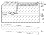
- FIG. 3C illustrates a process of forming a first polyimide layer 320 by coating a polyimide solution, which is one of plastic materials, on the carbon nanotube-graphene oxide layer 311.
- the first polyimide layer 320 may be formed to a first thickness.
- the buffer layer 330 may be formed by spraying an ink including carbon nanotubes on the first polyimide layer 320.
- the buffer layer 320 is an oxide thin film transistor array 340 to be formed on the first polyimide layer 320 by the external foreign matter such as moisture or oxygen penetrates the first polyimide layer 320 ) Can be prevented.
- the oxide thin film transistor array 340 may include at least one oxide thin film transistor 341 and a transistor driving array 342.
- At least one oxide thin film transistor 341 constituting the oxide thin film transistor array 340 may have a single gate electrode structure or may have a dual gate electrode structure.
- the oxide semiconductor layer is formed of amorphous indium gallium-zinc oxide (a-IGZO), zinc oxide (ZnO), indium zinc oxide (IZO), and indium tin oxide (ITO). ), Zinc tin oxide (ZTO), gallium zinc oxide (GZO), hafnium indium zinc oxide (HIZO), zinc indium tin oxide (ZITO), and aluminum zinc tin oxide (AZTO).
- a-IGZO amorphous indium gallium-zinc oxide
- ZnO zinc oxide
- IZO indium zinc oxide
- ITO indium tin oxide
- ZTO Zinc tin oxide
- GZO gallium zinc oxide
- ZITO zinc indium tin oxide
- AZTO aluminum zinc tin oxide
- the polyimide-based material constituting the second polyimide-based layer 350 may be a polyimide-based material having the same composition as the first polyimide-based layer 320.
- the second polyimide layer 350 may be formed to a second thickness.
- the first thickness of the first polyimide layer 320 and the second thickness of the second polyimide layer 350 may be the same or may be different from each other.
- the other layer may have a thickness within a range of 50% or less based on one layer.
- the first polyimide-based layer 320 is formed in the range of 50% or less of the thickness of the second polyimide-based layer 350, or the second polyimide-based layer 350 is the first polyimide-based layer 320 ) 50% or less of the thickness can be formed.
- the first thickness or the second thickness may be determined within the range of 1 ⁇ m to 30 ⁇ m, preferably 1 ⁇ m to 10 ⁇ m.
- 3G and 3H illustrate a process of forming at least one via contact 351 in the second polyimide layer 350.
- the via hole 351a is formed by etching a region to form the via contact 351.
- the via hole 351a is for exposing the source / drain electrodes and gate electrodes included in the oxide semiconductor transistor 340. In the actual process, a plurality of via holes 351a may be provided. Can be formed.
- the via contact 351 may be formed in the second polyimide layer 350 by filling the via hole 351a with a metal material.
- the via contact 351 is a component for electrically connecting the oxide semiconductor transistor 340 and the organic light emitting diode 360 to be formed through a subsequent process.
- FIG. 3I illustrates a process of forming the organic light emitting diode 360 on the second polyimide layer 360.
- the organic light emitting diode 360 may include at least one Active Matrix Organic Light-Emitting Diode (AMOLED) or at least one Organic Light-Emitting Diode (OLED).
- AMOLED Active Matrix Organic Light-Emitting Diode
- OLED Organic Light-Emitting Diode
- the organic light emitting diode 360 includes a pixel electrode 361, an organic light emitting layer 362 formed on the pixel electrode 361, an opposite electrode 363 formed on the organic light emitting layer 362, and an encapsulation layer 364.
- the pixel electrode 361 is in contact with the previously formed via contact 351 and electrically connected to the oxide thin film transistor 341. Therefore, the organic light emitting diode 360 may be driven under the control of the oxide thin film transistor 341 to emit light.
- FIG. 3J illustrates a process of removing the carrier substrate 310 from the carbon nanotube-graphene oxide layer 311.
- the carrier substrate 310 may be physically removed using a separate device.
- the flexible display apparatus 300 as illustrated in FIG. 3K may be manufactured.
- the flexible display apparatus 300 has a structure in which the oxide thin film transistor array 340 is positioned between the first polyimide layer 320 and the second polyimide layer 350 made of the same material.
- the oxide thin film transistor array 340 is positioned on a neutral plane substantially the same in compressive stress and tensile stress. Since the deformation does not occur at the neutral plane, even if the flexible display apparatus 300 is bent, the oxide thin film transistor array 340 may be prevented from being damaged by the compressive stress and the tensile stress.
- the flexible display device according to the comparative example and the embodiment is as follows.
- a flexible display device having a structure in which an oxide thin film transistor array and an organic light emitting diode are sequentially formed on one flexible substrate.
- an oxide thin film transistor is formed between the first polyimide layer and the second polyimide layer, and an organic light emitting diode is formed on the second polyimide layer. It is a flexible display device having a structure.
- the oxide thin film transistor may be positioned on a neutral plane having the same compressive stress and tensile stress between the first polyimide layer and the second polyimide layer.
- 4A and 4B illustrate current-voltage characteristics of an oxide thin film transistor included in each of the flexible display apparatuses of Comparative Examples and Examples, which are measured after removal of a carrier substrate in the flexible display apparatus.
- FIG. 4A illustrates two flexible display devices having different lower structures of an oxide thin film transistor.
- a flexible substrate PI (or a first polyimide-based layer PI1 and a carbon nanotube-graphene oxide layer) is disposed below the oxide thin film transistors TFTs.
- CNT-GO and a flexible display device having a first structure in which glass substrates are stacked in order, and a flexible substrate PI (or a first polyimide layer PI1) under the oxide thin film transistors TFTs.
- GO graphene oxide
- CNT carbon nanotubes
- the oxide thin film transistor included in the comparative example exhibits a log drain current of about ⁇ 12 at a gate voltage of 0 V and a log drain current of about ⁇ 6 A at a gate voltage of 20 V.
- the flexible substrate PI (or the first polyimide layer PI1 and the carbon nanotube-graphene oxide layer) is disposed below the oxide thin film transistors TFTs.
- CNT-GO and glass substrates are stacked in this order, and a first structure in which another flexible substrate PI (or a second polyimide layer PI2) is stacked on the oxide thin film transistors TFTs.
- a flexible display device having a dp flexible substrate (PI) (or a first polyimide-based layer (PI1), a carbon nanotube-graphene oxide layer (Carbon Nano Tube) Flexible display having a second structure in which Graphene Oxide (CNT-GO) is sequentially stacked and another flexible substrate (PI) (or second polyimide layer (PI2)) is stacked on top of oxide thin film transistors (TFTs).
- PI dp flexible substrate
- PI1 a first polyimide-based layer
- PI2 carbon nanotube-graphene oxide layer
- TFTs oxide thin film transistors
- the oxide thin film transistors included in the embodiment exhibit a log drain current of about ⁇ 14 at a gate voltage of 0 V and a log drain current of about ⁇ 6 A at a gate voltage of 20 V, compared with a comparative example. It has a high on-off ratio.
- the flexible display devices according to the comparative example have a high current-voltage characteristic when the second display has a second structure compared to the first structure.
- the flexible display devices according to the exemplary embodiment of FIG. 4B have no significant difference in current-voltage characteristics between the first structure and the second structure. This is because since the oxide thin film transistor is positioned between the first polyimide layer and the second polyimide layer, the oxide thin film transistor is not affected by the underlying structure.
- 5A and 5B illustrate current-voltage characteristics and field effect mobility of an oxide thin film transistor included in each of the flexible display apparatuses of the Comparative Examples and Examples, which are measured after the bending test of the flexible display apparatus.
- the bending radius was set to 0.25 mm during the bending test, and the number of bendings was accumulated to measure current-voltage characteristics of the oxide thin film transistor.
- the oxide thin film transistor included in the example has a high on-off ratio.
- FIGS. 6A and 6B illustrate electrical characteristics of an oxide thin film transistor included in each of the flexible display apparatuses of Comparative Examples and Examples, which are measured after a bending test of the flexible display apparatus.
- the bending radius is 0.25 mm, and the number of bendings is accumulated to change the ON voltage of the oxide thin film transistor ( ⁇ V ON ), the field effect mobility ( ⁇ FE ), and the sub-threshold swing. (Subthreshold Swing, SS) was specified.
- the on-voltage change ( ⁇ V ON ), the field effect mobility ( ⁇ FE ), and the sub-threshold swing (SS) were greatly changed as the number of bendings accumulated.
- the device is broken. This is because the stress is transferred to the oxide thin film transistor as the flexible display device repeatedly bends, causing cracks.
- the oxide thin film transistor included in the embodiment has no significant change in the ON voltage change ( ⁇ V ON ), the field effect mobility ( ⁇ FE ) and the sub-threshold swing (SS) even when the number of bendings is accumulated. Nevertheless, the flexible display device was not damaged. This is because in the flexible display device according to the embodiment, the oxide thin film transistor is positioned in a neutral plane to prevent deformation due to bending.
- FIG. 7 illustrates a flexible display device having a touch sensor.
- the flexible display apparatus 700 illustrated in FIG. 7 includes a first polyimide layer 710, an oxide thin film transistor array 720, a second polyimide layer 730, an AMOLED array 740, and an encapsulation layer 750. ) And touch sensor 760. That is, the flexible display apparatus 700 may be implemented as a touch type by providing the touch sensor 760.
- the oxide thin film transistor array 720 includes a plurality of oxide thin film transistors and a transistor driving circuit.
- the plurality of oxide thin film transistors may function as pixel elements and may be connected to transistor driving circuits.
- the transistor driving circuit may include a configuration such as a gate driver, a data driver, and a timing controller.
- the oxide thin film transistor array 720 is located at the neutral plane, the plurality of oxide thin film transistors and the transistor driving circuit are prevented from being damaged from stress from the outside. Therefore, it is not necessary to install the bezel (the device 700 boundary) to protect the transistor driving circuit located at the outer portion of the oxide thin film transistor array 720, thereby eliminating the process of installing the bezel and reducing the cost. Can be.
Landscapes
- Engineering & Computer Science (AREA)
- Microelectronics & Electronic Packaging (AREA)
- Chemical & Material Sciences (AREA)
- Materials Engineering (AREA)
- Nanotechnology (AREA)
- Physics & Mathematics (AREA)
- Geometry (AREA)
- Manufacturing & Machinery (AREA)
- Devices For Indicating Variable Information By Combining Individual Elements (AREA)
- Thin Film Transistor (AREA)
- Electroluminescent Light Sources (AREA)
Abstract
플렉서블 디스플레이 장치 및 그의 제조 방법을 제공한다. 본 발명의 플렉서블 디스플레이 장치는 캐리어 기판 상에 폴리이미드계 용액을 코팅하여 제1 폴리이미드계 층을 형성하는 단계, 제1 폴리이미드계 층 상에 산화물 박막 트랜지스터 어레이를 형성하는 단계, 산화물 박막 트랜지스터 어레이 상에 폴리이미드계 용액을 코팅하여 제2 폴리이미드계 층을 형성하는 단계, 제2 폴리이미드계 층 상에 유기 발광 다이오드를 형성하는 단계 및 캐리어 기판을 제거하는 단계를 포함하며, 산화물 박막 트랜지스터 어레이를 형성하는 단계는 상기 제1 폴리이미드계 층과 상기 제2 폴리이미드계 층 사이에 위치하도록 상기 산화물 박막 트랜지스터 어레이를 형성하는 산화물 박막 트랜지스터 어레이를 형성할 수 있다.
Description
본 발명은 외부로부터의 스트레스에 의해 산화물 박막 트래지스터 어레이가 손상되는 것을 방지하여 장치 수명 및 신뢰성을 향상시킨 플렉서블 디스플레이 장치 및 그의 제조 방법에 관한 것이다.
일반적으로 플렉시블 디스플레이 장치는 가요성 기판에 디스플레이부를 형성하여 유연성을 부가한 장치로서, 필요시 그 형태를 휘거나 구부려 사용할 수 있는 매우 유용한 장점을 가지고 있다. 이러한, 플렉서블 디스플레이 장치는 휴대용 컴퓨터나 전자신문, 스마트카드, 책, 신문, 잡지 등의 인쇄 매체를 대체하고 있는 차세대 표시장치로 기대되고 있다.
한편, 플렉서블 디스플레이 장치는 휨 발생시에도 표시 성능을 그대로 유지해야 함에도 불구하고, 휨의 정도에 따라 표시 성능의 불량이 발생하는 문제점을 발생시킨다.
특히, 플렉서블 디스플레이 장치는 플렉서블 기판 상에 전기 소자(예를 들어, 박막 트랜지스터 구조물)이 형성되는데, 플렉서블 디스플레이 장치의 휨이 크게 발생할 경우, 휨에 의한 스트레스가 전기 소자에 전달되어 크랙(crack)을 발생시키거나, 전기 소자의 특성을 저하시킨다. 이는 플렉서블 디스플레이 장치를 지나치게 구부리거나 반복적으로 구부릴 경우, 또는 플렉서블 디스플레이 장치가 대면적화될 경우 심화될 수 있으며, 결과적으로 플렉서블 디스플레이 장치의 수명 및 신뢰성을 떨어뜨린다.
본 발명은 플렉서블 디스플레이 장치를 구성하는 산화물 박막 트랜지스터 어레이를 중립면에 배치함으로써, 휨 또는 구부림 등의 스트레스에 의한 손상을 방지하여 장치의 수명 및 신뢰성을 향상시킨 플렉서블 디스플레이 장치 및 그의 제조 방법을 제공한다.
실시예에 따른 플렉서블 디스플레이 장치의 제조 방법은 캐리어 기판 상에 폴리이미드계 용액을 코팅하여 제1 폴리이미드계 층을 형성하는 단계, 상기 제1 폴리이미드계 층 상에 산화물 박막 트랜지스터 어레이를 형성하는 단계, 상기 산화물 박막 트랜지스터 어레이 상에 폴리이미드계 용액을 코팅하여 제2 폴리이미드계 층을 형성하는 단계, 상기 제2 폴리이미드계 층 상에 유기 발광 다이오드를 형성하는 단계 및 상기 캐리어 기판을 제거하는 단계를 포함하고, 상기 산화물 박막 트랜지스터 어레이를 형성하는 단계는 상기 제1 폴리이미드계 층과 상기 제2 폴리이미드계 층 사이에 위치하도록 상기 산화물 박막 트랜지스터 어레이를 형성한다.
상기 제2 폴리이미드계 층을 형성하는 단계는 상기 제1 폴리이미드계 층과 동일한 조성의 폴리이미드를 포함하는 폴리이미드계 용액으로 형성될 수 있다.
상기 플렉서블 디스플레이 장치의 제조 방법은 상기 제1 폴리이미드계 층 상에 탄소나노튜브를 포함하는 잉크를 분사하여 버퍼층을 형성하는 단계를 더 포함할 수 있다.
상기 제2 폴리이미드계 층을 형성하는 단계는 상기 제2 폴리이미드계 층을 관통하여, 상기 산화물 박막 트랜지스터 구조물과 상기 유기 발광 다이오드를 전기적으로 연결하기 위한 비아 컨택을 형성하는 단계를 포함할 수 있다.
상기 플렉서블 디스플레이 장치의 제조 방법은 상기 유기 발광 다이오드 구조물 상에 터치 센서를 형성하는 단계를 더 포함할 수 있다.
상기 제2 폴리이미드계 층을 형성하는 단계는 상기 제1 폴리이미드계 층과 동일한 두께로 형성할 수 있다.
상기 제1 폴리이미드계 층을 형성하는 단계는 상기 제2 폴리이미드계 층 두께의 50% 이하 범위로 형성할 수 있다.
상기 제2 폴리이미드계 층을 형성하는 단계는 상기 제1 폴리이미드계 층 두께의 50% 이하 범위로 형성할 수 있다.
상기 제1 폴리이미드계 층을 형성하는 단계 및 상기 제2 폴리이미드계 층을 형성하는 단계 각각은 1㎛ 내지 30㎛의 두께로 형성할 수 있다.
상기 제2 폴리이미드계 층을 형성하는 단계는 1㎛ 내지 10㎛의 두께로 형성할 수 있다.
상기 박막 트랜지스터 어레이를 형성하는 단계는 적어도 하나 이상의 산화물 박막 트랜지스터를 상기 제1 폴리이미드계 층 상에 형성할 수 있다.
실시예에 따른 플렉서블 디스플레이 장치는 폴리이미드계 물질로 이루어진 제1 폴리이미드계 층 상에 형성된 산화물 박막 트랜지스터 어레이, 상기 산화물 박막 트랜지스터 구조물 상에 형성된, 폴리이미드계 물질로 이루어진 제2 폴리이미드계 층 및 상기 제2 폴리이미드계 층 상에 형성된 유기 발광 다이오드를 포함하고, 상기 제1 폴리이미드계 층과 상기 제2 폴리이미드계 층 사이에 위치한다.
상기 제1 폴리이미드계 층 및 상기 제2 폴리이미드계 층을 구성하는 상기 폴리이미드계 물질은 동일한 조성의 폴리이미드 물질로 이루어질 수 있다.
상기 플렉서블 디스플레이 장치는 상기 제1 폴리이미드계 층과 상기 산화물 박막 트랜지스터 구조물 사이에 형성될 수 있다.
상기 제2 폴리이미드계 층은 상기 제2 폴리이미드계 층을 관통하여, 상기 산화물 박막 트랜지스터 구조물과 상기 유기 발광 다이오드를 전기적으로 연결하기 위한 비아 컨택을 포함할 수 있다.
상기 플렉서블 디스플레이 장치는 상기 유기 발광 다이오드 구조물 상에 형성된 터치 센서를 더 포함할 수 있다. 상기 제1 폴리이미드계 층 및 상기 제2 폴리이미드계 층은 동일한 두께로 형성될 수 있다.
상기 제1 폴리이미드계 층은 상기 제2 폴리이미드계 층 두께의 50% 이하 범위로 형성될 수 있다.
상기 제2 폴리이미드계 층은 상기 제1 폴리이미드계 층 두께의 50% 이하 범위로 형성될 수 있다.
본 발명에 따르면 플렉서블 디스플레이 장치는 산화물 박막 트랜지스터 어레이가 중립면에 위치하도록 두 개의 플렉서블 기판 사이에 배치시킴으로써, 외부 스트레스에 의해 산화물 박막 트랜지스터 어레이가 손상되는 것을 방지하여 장치 수명 및 신뢰성을 향상시킬 수 있다. 특히, 플렉서블 디스플레이 장치가 반복적으로 휘어지더라도, 중립면에 위치된 산화물 박막 트랜지스터 어레이는 스트레스의 영향을 받지 않을 수 있다.
도 1a 및 도 1b는 본 발명의 실시예에 따른 플렉서블 디스플레이 장치를 도시한 것이다.
도 2는 본 발명의 다른 실시예에 따른 플렉서블 디스플레이 장치를 도시한 것이다.
도 3a 내지 도 3k는 본 발명의 실시예에 따른 플렉서블 디스플레이 장치의 제조 과정을 도시한 것이다.
도 4a 및 도 4b는 캐리어 기판 제거 후에 측정한, 비교예 및 실시예 각각의 플렉서블 디스플레이 장치에 포함된 산화물 박막 트랜지스터의 전류-전압 특성을 도시한 것이다.
도 5a 및 도 5b는 플렉서블 디스플레이 장치를 벤딩 테스트(bending test)한 후에 측정한, 비교예 및 실시예 각각의 플렉서블 디스플레이 장치에 포함된 산화물 박막 트랜지스터의 전류-전압 특성 및 전계효과이동도를 도시한 것이다.
도 6a 및 도 6b는 플렉서블 디스플레이 장치를 벤딩 테스트(bending test)한 후에 측정한, 비교예에 따른 산화물 박막 트랜지스터와, 실시예에 따른 산화물 박막 트랜지스터의 전기적 특성을 도시한 것이다.
도 7은 터치 센서를 구비한 플렉서블 디스플레이 장치를 도시한 것이다.
이하 첨부 도면들 및 첨부 도면들에 기재된 내용들을 참조하여 본 발명의 실시예를 상세하게 설명하지만, 본 발명이 실시예에 의해 제한되거나 한정되는 것은 아니다.
소자(elements) 또는 층이 다른 소자 또는 층의 "위(on)" 또는 "상(on)"으로 지칭되는 것은 다른 소자 또는 층의 바로 위뿐만 아니라 중간에 다른 층 또는 다른 소자를 개재한 경우를 모두 포함한다. 반면, 소자가 ""직접 위(directly on)" 또는 "바로 위"로 지칭되는 것은 중간에 다른 소자 또는 층을 개재하지 않은 것을 나타낸다.
공간적으로 상대적인 용어인 "아래(below)", "아래(beneath)", "하부(lower)", "위(above)", "상부(upper)" 등은 도면에 도시되어 있는 바와 같이 하나의 소자 또는 구성 요소들과 다른 소자 또는 구성 요소들과의 상관관계를 용이하게 기술하기 위해 사용될 수 있다. 공간적으로 상대적인 용어는 도면에 도시되어 있는 방향에 더하여 사용시 또는 동작시 소자의 서로 다른 방향을 포함하는 용어로 이해되어야 한다. 예를 들면, 도면에 도시되어 있는 소자를 뒤집을 경우, 다른 소자의 "아래(below 또는 beneath)"로 기술된 소자는 다른 소자의 "위(above)"에 놓여질 수 있다. 따라서, 예시적인 용어인 "아래"는 아래와 위의 방향을 모두 포함할 수 있다. 소자는 다른 방향으로도 배향될 수 있으며, 이 경우 공간적으로 상대적인 용어들은 배향에 따라 해석될 수 있다.
본 명세서에서 사용된 용어는 실시예들을 설명하기 위한 것이며 본 발명을 제한하고자 하는 것은 아니다. 본 명세서에서, 단수형은 문구에서 특별히 언급하지 않는 한 복수형도 포함한다. 명세서에서 사용되는 "포함한다(comprises)" 및/또는 "포함하는(comprising)"은 언급된 구성요소, 단계, 동작 및/또는 소자는 하나 이상의 다른 구성요소, 단계, 동작 및/또는 소자의 존재 또는 추가를 배제하지 않는다.
다른 정의가 없다면, 본 명세서에서 사용되는 모든 용어(기술 및 과학적 용어를 포함)는 본 발명이 속하는 기술분야에서 통상의 지식을 가진 자에게 공통적으로 이해될 수 있는 의미로 사용될 수 있을 것이다. 또 일반적으로 사용되는 사전에 정의되어 있는 용어들은 명백하게 특별히 정의되어 있지 않는 한 이상적으로 또는 과도하게 해석되지 않는다.
한편, 본 발명을 설명함에 있어서, 관련된 공지 기능 또는 구성에 대한 구체적인 설명이 본 발명의 요지를 불필요하게 흐릴 수 있다고 판단되는 경우에는, 그 상세한 설명을 생략할 것이다. 그리고, 본 명세서에서 사용되는 용어(terminology)들은 본 발명의 실시예를 적절히 표현하기 위해 사용된 용어들로서, 이는 사용자, 운용자의 의도 또는 본 발명이 속하는 분야의 관례 등에 따라 달라질 수 있다. 따라서, 본 용어들에 대한 정의는 본 명세서 전반에 걸친 내용을 토대로 내려져야 할 것이다.
도 1a 및 도 1b는 본 발명의 실시예에 따른 플렉서블 디스플레이 장치를 도시한 것이다. 도 1a 및 도 1b에 도시된 플렉서블 디스플레이 장치(100)는 제1 폴리이미드계 층(110), 산화물 박막 트랜지스터 어레이(120), 제2 폴리이미드계 층(130) 및 유기 발광 다이오드 (140)를 포함한다.
플렉서블 디스플레이 장치(100)에서 제1 및 제2 폴리이미드계 층(110, 130)은그들 사이에 위치된 산화물 박막 트랜지스터 어레이(120)를 보호한다.
제1 및 제2 폴리이미드계 층(110, 130)는 폴리이미드계 물질로 이루이지며, 서로 동일한 물질 조성을 가질 수 있다. 또한, 제1 및 제2 폴리이미드계 층(110, 130)는 동일한 두께로 형성될 수도 있고, 서로 상이한 두께로 형성될 수도 있다.
상술한 구조에 의해 산화물 박막 트랜지스터 어레이(120)는 제1 폴리이미드계 층(110)과 제2 폴리이미드계 층(130) 사이에 위치함에 따라, 압축 응력 및 인장 응력이 동일한 중립면(Neutral Plane, NP)에 위치한다.
도 1b와 같이, 플렉서블 디스플레이 장치(100)가 휘어지면, 제1 폴리이미드계 층(110)에는 인장 응력이 작용하고 제2 폴리이미드계 층(130)에는 압축 응력이 작용하는데, 중립면(NP)에서는 실질적으로 인장도 압축도 이루어지지 않기 때문에 실질적으로 변형이 일어나지 않는다. 따라서, 플렉서블 디스플레이 장치(100)가 휘어지더라도, 중립면(NP)에 위치된 산화물 박막 트랜지스터 어레이(120)가 변형되지 않기 때문에 산화물 박막 트랜지스터 어레이(120)의 전기적 특성이 저하되거나, 손상되는 것을 방지할 수 있다.
도 2는 본 발명의 다른 실시예에 따른 플렉서블 디스플레이 장치를 도시한 것이다. 도 2에 도시된 플렉서블 디스플레이 장치(200)는 제1 폴리이미드계 층(110), 산화물 박막 트랜지스터 어레이(120), 제2 폴리이미드계 층(130) 및 유기 발광 다이오드 (140)를 포함한다.
도 2에 도시된 플렉서블 디스플레이 장치(200)는 탄소나노튜브-그래핀 산화물층(210), 제1 폴리이미드계 층(220), 버퍼층(230), 산화물 박막 트랜지스터 어레이(240), 제2 폴리이미드계 층(220) 및 유기 발광 다이오드 (260)를 포함할 수 있다.
탄소나노튜브-그래핀 산화물층(Carbon Nano Tube-Graphene Oxide, CNT-GO)(210)는 투명성을 갖는 지지층이다. 이 탄소나노튜브-그래핀 산화물층(210)은 휘어지는 성질이 있어 플렉서블 디스플레이 장치(200)에 적합한 구성이다.
제1 폴리이미드계 층(220)은 폴리이미드계 물질로 형성된다.
산화물 박막 트랜지스터 어레이(240)는 적어도 하나의 산화물 박막 트랜지스터(241) 및 트랜지스터 구동 어레이(242)를 포함한다. 여기서, 적어도 하나 이상의 산화물 박막 트랜지스터(241)는 단일 게이트 전극 구조를 갖거나, 듀얼 게이트 전극 구조를 가질 수 있다.
제2 폴리이미드계 층(250)은 제1 폴리이미드계 층(220)과 동일한 조성을 갖는 폴리이미드계 물질로 형성되며, 제1 폴리이미드계 층(220)과 동일한 두께를 갖는다. 여기서, 제1 폴리이미드계 층(220) 및 제2 폴리이미드계 층(250)의 두께는 1㎛ 내지 30㎛ 범위 내에서 정해질 수 있으며, 바람직하게는 1㎛ 내지 10㎛ 범위 내에서 정해질 수 있다. 따라서, 제1 폴리이미드계 층(220)과 제2 폴리이미드계 층(250)은 동일한 탄성률을 가질 수 있으며, 제1 폴리이미드계 층(220)과 제2 폴리이미드계 층(250) 사이에 위치한 산화물 박막 트랜지스터 어레이(240)에 중립면이 위치하게 된다.
산화물 박막 트랜지스터 어레이(240)가 중립면에 위치함으로써, 플렉서블 디스플레이 장치(200)가 휘어지더라도 산화물 박막 트랜지스터 어레이(240)는 길이나 부피 등의 변화가 없는 것으로, 휨에 의한 스트레스를 방지 않는다. 특히, 플렉서블 디스플레이 장치(200)의 휘어지는 횟수가 누적되더라도 산화물 박막 트랜지스터 어레이(240)가 변형되지 않기 때문에, 산화물 박막 트랜지스터 어레이(240)에 크랙이 발생하여 수명이 짧아지거나 전기적 신뢰성이 저하되지 않는다.
한편, 제2 폴리이미드계 층(250)은 비아 컨택(251)을 포함하는데, 이 비아 컨택(251)은 산화물 박막 트랜지스터(241)에 포함된 소스/드레인 전극 및 게이트 전극에 접촉될 수 있다. 또한, 이 비아 컨택(251)은 제2 폴리이미드계 층(250)의 상부에 형성된 유기 발광 다이오드 (260)에 포함된 화소 전극(261)과 접촉될 수 있다. 즉, 비아 컨택(251)은 산화물 박막 트랜지스터 어레이(240)와 유기 발광 다이오드 (260)를 전기적으로 연결하게 된다. 여기서, 유기 발광 다이오드(260)는 제2 폴리이미드계 층(250) 상에 하나 이상이 형성될 수 있다.
유기 발광 다이오드 (260)는 화소 전극(261), 화소 전극(261) 상에 형성된 유기 발광층(262), 유기 발광층(262) 상에 형성된 대향 전극(263) 및 봉지층(264)을 포함한다. 여기서, 화소 전극(261)은 앞서 형성된 비아 컨택(351)과 접촉되어 산화물 박막 트랜지스터(241)와 전기적으로 연결된다.
여기서, 화소 전극(261)은 애노드(anode) 전극이고, 대향 전극(263)은 캐소드(cathod) 전극이 될 수 있으며, 그 반대가 될 수도 있다. 화소 전극(261) 및 대향 전극(263)에 전압이 인가되면 각각 정공과 전자가 유기 발광층(262) 내부로 주입됨에 따라 유기 발광층(262)에서 광이 방출된다.
도 3a 내지 도 3j는 본 발명의 실시예에 따른 플렉서블 디스플레이 장치의 제조 과정을 도시한 것이다.
도 3a 및 도 3b는 캐리어 기판(310) 상에, 탄소나노튜브(Carbon Nano Tube, CNT)가 함유된 그래핀 산화물(Graphene Oxide)을 코팅하여 탄소나노튜브-그래핀 산화물층(311)을 형성하는 공정을 도시한 사시도 및 단면도이다.
캐리어 기판(310)은 다공성 세라믹 물질로 이루어질 수 있다. 다공성 세라믹 물질은 고온에서 안정적이며 기계적 강도가 강한 특성을 갖기 때문에, 플렉서블 디스플레이 장치의 제조 공정 중에 적용되는 온도 및 충격에 의한 캐리어 기판(310)의 변형을 방지할 수 있다.
탄소나노튜브-그래핀 산화물층(311)은 탄소나노튜브가 분산된 용액을 캐리어 기판(310) 상에 스핀 코팅한 후, 탄소나노튜브 상에 그래핀 산화물을 증착하는 방식으로 형성될 수 있다.
도 3c는 탄소나노튜브-그래핀 산화물층(311) 상에, 플라스틱 재질 중 하나인 폴리이미드계 용액을 코팅하여 제1 폴리이미드계 층(320)을 형성하는 공정을 도시한 것이다. 여기서, 제1 폴리이미드계 층(320)은 제1 두께로 형성될 수 있다.
도 3d는 제1 폴리이미드계 층(320) 상에 버퍼층(330)을 형성하는 공정을 도시한 것이다. 버퍼층(330)은 탄소나노튜브를 포함하는 잉크를 제1 폴리이미드계 층(320) 상에 분사시키는 방식으로 형성될 수 있다.
본 발명에서, 버퍼층(320)은 수분이나 산소와 같은 외부의 이물질이 제1 폴리이미드계 층(320)을 투과하여, 제1 폴리이미드계 층(320) 상에 형성될 산화물 박막 트랜지스터 어레이(340)에 침투하는 것을 방지할 수 있다.
도 3e는 제1 폴리이미드계 층(320) 상에 산화물 박막 트랜지스터 어레이(340)를 형성하는 공정을 도시한 것이다. 여기서, 산화물 박막 트랜지스터 어레이(340)는 적어도 하나 이상의 산화물 박막 트랜지스터(341) 및 트랜지스터 구동 어레이(342)를 포함할 수 있다.
여기서, 산화물 박막 트랜지스터 어레이(340)를 구성하는 적어도 하나 이상의 산화물 박막 트랜지스터(341)는 단일 게이트 전극 구조를 갖거나, 듀얼 게이트 전극 구조를 가질 수 있다.
또한, 산화물 박막 트랜지스터(341)에서 산화물 반도체층은 비정질 인듐 갈륨 징크 옥사이드(amorphous indium-gallium-zinc oxide, a-IGZO), 징크 옥사이드(ZnO), 인듐 징크 옥사이드(IZO), 인듐 틴 옥사이드(ITO), 징크 틴 옥사이드(ZTO), 갈륨 징크 옥사이드(GZO), 하프늄 인듐 징크 옥사이드(HIZO), 징크 인듐 틴 옥사이드(ZITO) 및 알루미늄 징크 틴 옥사이드(AZTO) 중 어느 하나를 포함할 수 있다.
도 3f는 산화물 박막 트랜지스터 어레이(340) 상에 폴리이미드계 용액을 코팅하여 제2 폴리이미드계 층(350)을 형성하는 공정을 도시한 것이다. 제2 폴리이미드계 층(350)을 구성하는 폴리이미드계 물질은 제1 폴리이미드계 층(320)과 동일한 조성의 폴리이미드계 물질일 수 있다.
또한, 제2 폴리이미드계 층(350)은 제2 두께로 형성될 수 있다. 여기서, 제1 폴리이미드계 층(320)의 제1 두께와 제2 폴리이미드계 층(350)의 제2 두께는 동일할 수 있으며, 서로 다를 수도 있다.
제1 두께와 제2 두께가 서로 다른 두께를 갖는 경우, 어느 하나의 층을 기준으로 다른 하나의 층은 50% 이하의 범위 내에서 두께가 정해질 수 있다. 구체적으로, 제1 폴리이미드계 층(320)이 제2 폴리이미드계 층(350) 두께의 50% 이하 범위로 형성되거나, 제2 폴리이미드계 층(350)이 제1 폴리이미드계 층(320) 두께의 50% 이하 범위로 형성될 수 있다.
여기서, 제1 두께 또는 제2 두께는 1㎛ 내지 30㎛ 범위 내에서 정해질 수 있으며, 바람직하게는 1㎛ 내지 10㎛ 범위 내에서 정해질 수 있다. 도 3g 및 도 3h는 제2 폴리이미드계 층(350)에 적어도 하나의 비아 컨택(351)을 형성하는 공정을 도시한 것이다. 먼저, 제2 폴리이미드계 층(350)에서, 비아 컨택(351)을 형성할 영역을 식각하여 비아홀(351a)을 형성한다. 도면 상에서는 하나의 비아홀(351a)만 도시되어 있으나, 비아홀(351a)은 산화물 반도체 트랜지스터(340)에 포함된 소스/드레인 전극, 게이트 전극을 노출시키기 위한 것으로, 실제 공정에서 비아홀(351a)은 여러 개가 형성될 수 있다.
이후, 비아홀(351a)에 금속 물질을 충전시켜 제2 폴리이미드계 층(350) 내에 비아 컨택(351)을 형성할 수 있다. 여기서, 비아 컨택(351)은 산화물 반도체 트랜지스터(340)와, 이후 공정을 통해 형성될 유기 발광 다이오드 (360)를 전기적으로 연결하기 위한 구성이다.
도 3i는 제2 폴리이미드계 층(360) 상에 유기 발광 다이오드 (360)를 형성하는 공정을 도시한 것이다. 유기 발광 다이오드 (360)는 적어도 하나의 AMOLED(Active Matrix Organic Light-Emitting Diode) 또는 적어도 하나의 OLED(Organic Light-Emitting Diode)를 포함할 수 있다. 이하에서는, 유기 발광 다이오드 (360)가 1개의 AMOLED를 포함하는 형태를 예로 들어 설명한다.
유기 발광 다이오드 (360)는 화소 전극(361), 화소 전극(361) 상에 형성된 유기 발광층(362), 유기 발광층(362) 상에 형성된 대향 전극(363) 및 봉지층(364)을 포함한다. 여기서, 화소 전극(361)은 앞서 형성된 비아 컨택(351)과 접촉되어 산화물 박막 트랜지스터(341)와 전기적으로 연결된다. 따라서, 유기 발광 다이오드 (360)는 산화물 박막 트랜지스터(341)의 제어에 따라 구동되어 광을 방출할 수 있다.
도 3j는 탄소나노튜브-그래핀 산화물층(311)으로부터 캐리어 기판(310)을 제거하는 공정을 도시한 것이다. 캐리어 기판(310)은 별도의 장치를 이용하여 물리적으로 제거될 수 있다.
상술한 공정 순서에 의해 도 3k에 도시된 것과 같은 플렉서블 디스플레이 장치(300)를 제조할 수 있다. 플렉서블 디스플레이 장치(300)는 동일 물질로 이루어진 제1 폴리이미드계 층(320)과 제2 폴리이미드계 층(350) 사이에 산화물 박막 트랜지스터 어레이(340)가 위치된 구조를 갖는다. 이때, 산화물 박막 트랜지스터 어레이(340)는 압축 응력 및 인장 응력이 실질적으로 동일한 중립면에 위치하게 된다. 중립면에서는 변형이 일어나지 않기 때문에, 플렉서블 디스플레이 장치(300)가 휘어지더라도 압축 응력 및 인장 응력에 의해 산화물 박막 트랜지스 어레이(340)가 손상되는 것을 방지할 수 있다.
이하, 도 4 내지 도 6은 비교예에 따른 플렉서블 디스플레이 장치에 포함된 산화물 박막 트랜지스터와, 본 발명의 실시예에 따른 플렉서블 디스플레이 장치에 포함된 산화물 박막 트랜지스터의 전기적 특성을 측정한 실험 데이터들에 기반한 그래프이다. 여기서, 비교예와 실시예에 따른 플렉서블 디스플레이 장치는 아래와 같다.
<비교예>
하나의 플렉서블 기판 상에 산화물 박막 트랜지스터 어레이 및 유기 발광 다이오드가 순차적으로 형성된 구조를 갖는 플렉서블 디스플레이 장치이다.
<실시예>
도 3a 내지 도 3k에 도시된 공정에 의해 제조된 것으로, 제1 폴리이미드계 층과 제2 폴리이미드계 층 사이에 산화물 박막 트랜지스터가 형성되며, 제2 폴리이미드계 층 상에 유기 발광 다이오드가 형성된 구조를 갖는 플렉서블 디스플레이 장치이다. 여기서, 산화물 박막 트랜지스터는 제1 폴리이미드계 층과 제2 폴리이미드계 층 사이에서 압축 응력 및 인장 응력이 동일한 중립면에 위치될 수 있다.
도 4a 및 도 4b는 플렉서블 디스플레이 장치에서 캐리어 기판 제거 후에 측정한, 비교예 및 실시예 각각의 플렉서블 디스플레이 장치에 포함된 산화물 박막 트랜지스터의 전류-전압 특성을 도시한 것이다.
도 4a는 산화물 박막 트랜지스터의 하부 구조가 다른 2개의 플렉서블 디스플레이 장치를 이용하였다. 구체적으로, 도 4a를 참조하면, 산화물 박막 트랜지스터(TFTs)의 하부에 플렉서블 기판(PI)(또는 제1 폴리이미드계 층(PI1), 탄소나노튜브-그래핀 산화물층(Carbon Nano Tube-Graphene Oxide, CNT-GO), 유리 기판(Glass)이 순서대로 적층된 제1 구조를 갖는 플렉서블 디스플레이 장치와, 산화물 박막 트랜지스터(TFTs)의 하부에 플렉서블 기판(PI)(또는 제1 폴리이미드계 층(PI1), 그래핀 산화물(Graphene Oxide, GO), 탄소나노튜브(Caborn Nano Tube, CNT)가 순서대로 적층된 제2 구조를 갖는 플렉서블 디스플레이 장치를 이용하였다.
도 4a를 참조하면, 비교예에 포함된 산화물 박막 트랜지스터는 0V의 게이트 전압에서 약 -12의 로그 드레인 전류를 나타내고, 20V의 게이트 전압에서 약 -6A의 로그 드레인 전류를 나타낸다.
도 4b 역시 산화물 박막 트랜지스터의 하부 구조가 다른 2개의 플렉서블 디스플레이 장치를 이용하였다. 구체적으로, 도 4b를 참조하면, 산화물 박막 트랜지스터(TFTs)의 하부에 플렉서블 기판(PI)(또는 제1 폴리이미드계 층(PI1), 탄소나노튜브-그래핀 산화물층(Carbon Nano Tube-Graphene Oxide, CNT-GO), 유리 기판(Glass)이 순서대로 적층되고, 산화물 박막 트랜지스터(TFTs)의 상부에 또 다른 플렉서블 기판(PI)(또는 제2 폴리이미드계 층(PI2)이 적층된 제1 구조를 갖는 플렉서블 디스플레이 장치를 이용하였다. 또한, 산화물 박막 트랜지스터(TFTs)의 하부dp 플렉서블 기판(PI)(또는 제1 폴리이미드계 층(PI1), 탄소나노튜브-그래핀 산화물층(Carbon Nano Tube-Graphene Oxide, CNT-GO)가 순서대로 적층되고, 산화물 박막 트랜지스터(TFTs)의 상부에 또 다른 플렉서블 기판(PI)(또는 제2 폴리이미드계 층(PI2)이 적층된 제2 구조를 갖는 플렉서블 디스플레이 장치를 이용하였다.
도 4b를 참조하면, 실시예에 포함된 산화물 박막 트랜지스터들은 0V의 게이트 전압에서 약 -14의 로그 드레인 전류를 나타내고, 20V의 게이트 전압에서 약 -6A의 로그 드레인 전류를 나타내는 것으로, 비교예에 비해 높은 on-off 비율을 갖는다.
한편, 도 4a를 참조하면, 비교예에 따른 플렉서블 디스플레이 장치들은 제1 구조에 비해 제2 구조를 가질 때 높은 전류-전압 특성을 갖는다. 반면, 도 4b에서 실시예에 따른 플렉서블 디스플레이 장치들은 제1 구조와 제2 구조에서 전류-전압 특성에 큰 차이가 없다. 이는 제1 폴리이미드계 층과 제2 폴리이미드계 층 사이에 산화물 박막 트랜지스터가 위치하기 때문에, 산화물 박막 트랜지스터는 그 하부 구조에 따른 영향을 받지 않음을 알 수 있다.
도 5a 및 도 5b는 플렉서블 디스플레이 장치를 벤딩 테스트(bending test)한 후에 측정한, 비교예 및 실시예 각각의 플렉서블 디스플레이 장치에 포함된 산화물 박막 트랜지스터의 전류-전압 특성 및 전계효과이동도를 도시한 것이다. 이때, 벤딩 테스트(bending test)시 벤딩 반경(beding radius)을 0.25㎜으로 하고, 벤딩 횟수를 누적하여 산화물 박막 트랜지스터의 전류-전압 특성을 측정하였다.
비교예에 포함된 산화물 박막 트랜지스터에 비해, 실시예에 포함된 산화물 박막 트랜지스터가 높은 on-off 비율을 갖는다. 특히, 벤딩 횟수가 증가할 수록 실시예에 따른 산화물 박막 트랜지스터의 전류-전압 특성 및 전계효과이동도가 향상됨을 알 수 있다.
도 6a 및 도 6b는 플렉서블 디스플레이 장치를 벤딩 테스트(bending test)한 후에 측정한, 비교예 및 실시예 각각의 플렉서블 디스플레이 장치에 포함된 산화물 박막 트랜지스터의 전기적 특성을 도시한 것이다. 이때, 벤딩 테스트(bending test)시 벤딩 반경(beding radius)을 0.25㎜으로 하고, 벤딩 횟수를 누적하여 산화물 박막 트랜지스터의 온 전압 변화(ΔVON), 전계효과이동도(μFE) 및 서브문턱스윙(Subthreshold Swing, SS)를 특정하였다.
비교예에 포함된 산화물 박막 트랜지스터는 벤딩 횟수가 누적됨에 따라 온 전압 변화(ΔVON), 전계효과이동도(μFE) 및 서브문턱스윙(SS)이 크게 변화되었으며, 특히 5000회 벤딩시 플렉서블 디스플레이 장치가 파손되었다. 이는 플렉서블 디스플레이 장치가 반복 벤딩되면서 이 스트레스가 산화물 박막 트랜지스터에 전달되어 크랙을 발생시키기 때문이다.
반면, 실시예에 포함된 산화물 박막 트랜지스터는 벤딩 횟수가 누적되더라도 온 전압 변화(ΔVON), 전계효과이동도(μFE) 및 서브문턱스윙(SS)에 큰 변화가 없으며, 특히 20000회의 벤딩에도 불구하고 플렉서블 디스플레이 장치가 파손되지 않았다. 이는 실시예에 따른 플렉서블 디스플레이 장치에서, 산화물 박막 트랜지스터가 중립면(neutral plane)에 위치되어 벤딩에 의한 변형이 방지되기 때문이다.
도 7은 터치 센서를 구비한 플렉서블 디스플레이 장치를 도시한 것이다.
도 7에 도시된 플렉서블 디스플레이 장치(700)는 제1 폴리이미드계 층(710), 산화물 박막 트랜지스터 어레이(720), 제2 폴리이미드계 층(730), AMOLED 어레이(740), 봉지층(750) 및 터치 센서(760)을 포함한다. 즉, 플렉서블 디스프레이 장치(700)는 터치 센서(760)를 구비함으로써, 터치 타입으로 구현될 수 있다.
산화물 박막 트랜지스터 어레이(720)는 복수의 산화물 박막 트랜지스터 및 트랜지스터 구동 회로를 포함한다. 복수의 산화물 박막 트랜지스터는 화소 소자로 기능할 수 있으며, 트랜지스터 구동 회로에 연결될 수 있다. 또한, 트랜지스터 구동 회로는 게이트 구동부, 데이터 구동부 및 타이밍 제어부 등의 구성을 포함할 수 있다.
도 7에서, 산화물 박막 트랜지스터 어레이(720)가 중립면에 위치하기 때문에 복수의 산화물 박막 트랜지스터 및 트랜지스터 구동 회로가 외부로부터의 스트레스로부터 손상되는 것이 방지된다. 따라서, 산화물 박막 트랜지스터 어레이(720)의 외곽 부분에 위치하는 트랜지스터 구동 회로를 보호하기 위하여 베젤(장치(700) 테투리)을 설치할 필요가 없기 때문에, 베젤 설치에 따른 공정을 생략하고 그 비용을 절감할 수 있다.
이상과 같이 실시예들이 비록 한정된 실시예와 도면에 의해 설명되었으나, 해당 기술분야에서 통상의 지식을 가진 자라면 상기의 기재로부터 다양한 수정 및 변경이 가능하다. 예를 들어, 설명된 기술들이 설명된 방법과 다른 순서로 수행되거나, 및/또는 설명된 시스템, 구조, 장치, 회로 등의 구성요소들이 설명된 방법과 다른 형태로 결합 또는 조합되거나, 다른 구성요소 또는 균등물에 의하여 대치되거나 치환되더라도 적절한 결과가 달성될 수 있다.
그러므로, 다른 구현들, 다른 실시예들 및 특허청구범위와 균등한 것들도 후술하는 특허청구범위의 범위에 속한다.
Claims (19)
- 캐리어 기판 상에 폴리이미드계 용액을 코팅하여 제1 폴리이미드계 층을 형성하는 단계;상기 제1 폴리이미드계 층 상에 산화물 박막 트랜지스터 어레이를 형성하는 단계;상기 산화물 박막 트랜지스터 어레이 상에 폴리이미드계 용액을 코팅하여 제2 폴리이미드계 층을 형성하는 단계;상기 제2 폴리이미드계 층 상에 유기 발광 다이오드를 형성하는 단계; 및상기 캐리어 기판을 제거하는 단계;를 포함하고,상기 산화물 박막 트랜지스터 어레이를 형성하는 단계는,상기 제1 폴리이미드계 층과 상기 제2 폴리이미드계 층 사이에 위치하도록 상기 산화물 박막 트랜지스터 어레이를 형성하는, 플렉서블 디스플레이 장치의 제조 방법.
- 제1항에 있어서,상기 제2 폴리이미드계 층을 형성하는 단계는,상기 제1 폴리이미드계 층과 동일한 조성의 폴리이미드를 포함하는 폴리이미드계 용액으로 형성되는, 플렉서블 디스플레이 장치의 제조 방법.
- 제1항에 있어서,상기 제1 폴리이미드계 층 상에 탄소나노튜브를 포함하는 잉크를 분사하여 버퍼층을 형성하는 단계;를 더 포함하는 플렉서블 디스플레이 장치의 제조 방법.
- 제1항에 있어서,상기 제2 폴리이미드계 층을 형성하는 단계는,상기 제2 폴리이미드계 층을 관통하여, 상기 산화물 박막 트랜지스터 구조물과 상기 유기 발광 다이오드를 전기적으로 연결하기 위한 비아 컨택을 형성하는 단계를 포함하는 플렉서블 디스플레이 장치의 제조 방법.
- 제1항에 있어서,상기 유기 발광 다이오드 구조물 상에 터치 센서를 형성하는 단계;를 더 포함하는 플렉서블 디스플레이 장치의 제조 방법.
- 제1항에 있어서,상기 제2 폴리이미드계 층을 형성하는 단계는,상기 제1 폴리이미드계 층과 동일한 두께로 형성하는, 플렉서블 디스플레이 장치의 제조 방법.
- 제1항에 있어서,상기 제1 폴리이미드계 층을 형성하는 단계는,상기 제2 폴리이미드계 층 두께의 50% 이하 범위로 형성하는, 플렉서블 디스플레이 장치의 제조 방법.
- 제1항에 있어서,상기 제2 폴리이미드계 층을 형성하는 단계는,상기 제1 폴리이미드계 층 두께의 50% 이하 범위로 형성하는, 플렉서블 디스플레이 장치의 제조 방법.
- 제6항 내지 제8항 중 어느 한 항에 있어서,상기 제1 폴리이미드 층을 형성하는 단계 및 제2 폴리이미드계 층을 형성하는 단계 각각은,1㎛ 내지 30㎛의 두께로 형성하는, 플렉서블 디스플레이 장치의 제조 방법.
- 제9항에 있어서,상기 제1 폴리이미드계 층을 형성하는 단계 및 제2 폴리이미드계 층을 형성하는 단계 각각은,1㎛ 내지 10㎛의 두께로 형성하는, 플렉서블 디스플레이 장치의 제조 방법.
- 제1항에 있어서,상기 박막 트랜지스터 어레이를 형성하는 단계는,적어도 하나 이상의 산화물 박막 트랜지스터를 상기 제1 폴리이미드계 층 상에 형성하는, 플렉서블 디스플레이 장치의 제조 방법.
- 폴리이미드계 물질로 이루어진 제1플렉서블 기판 상에 형성된 산화물 박막 트랜지스터 구조물;상기 산화물 박막 트랜지스터 구조물 상에 형성된, 폴리이미드계 물질로 이루어진 제2 폴리이미드계 층; 및상기 제2 폴리이미드계 층 상에 형성된 유기 발광 다이오드를 포함하고,상기 박막 트랜지스터 어레이는,상기 제1 폴리이미드계 층과 상기 제2 폴리이미드계 층 사이에 위치하는, 플렉서블 디스플레이 장치.
- 제12항에 있어서,상기 제1 폴리이미드계 층 및 상기 제2 폴리이미드계 층을 구성하는 상기 폴리이미드계 물질은 동일한 조성의 폴리이미드 물질로 이루어진, 플렉서블 디스플레이 장치.
- 제12항에 있어서,상기 제1 폴리이미드계 층과 상기 산화물 박막 트랜지스터 구조물 사이에 형성된, 탄소나노튜브를 포함하는 버퍼층;을 더 포함하는 플렉서블 디스플레이 장치.
- 제12항에 있어서,상기 제2 폴리이미드계 층은,상기 제2 폴리이미드계 층을 관통하여, 상기 산화물 박막 트랜지스터 구조물과 상기 유기 발광 다이오드를 전기적으로 연결하기 위한 비아 컨택을 포함하는 플렉서블 디스플레이 장치.
- 제12항에 있어서,상기 유기 발광 다이오드 구조물 상에 형성된 터치 센서;를 더 포함하는 플렉서블 디스플레이 장치.
- 제12항에 있어서,상기 제1 폴리이미드계 층 및 상기 제2 폴리이미드계 층은 동일한 두께로 형성된, 플렉서블 디스플레이 장치.
- 제12항에 있어서,상기 제1 폴리이미드계 층은,상기 제2 폴리이미드계 층 두께의 50% 이하 범위로 형성되는, 플렉서블 디스플레이 장치.
- 제12항에 있어서,상기 제2 폴리이미드계 층은,상기 제1 폴리이미드계 층 두께의 50% 이하 범위로 형성되는, 플렉서블 디스플레이 장치.
Priority Applications (2)
| Application Number | Priority Date | Filing Date | Title |
|---|---|---|---|
| CN201680083178.4A CN108886110B (zh) | 2016-01-04 | 2016-11-29 | 柔性显示装置及其制造方法 |
| US15/741,542 US10305051B2 (en) | 2016-01-04 | 2016-11-29 | Flexible display device and method of manufacturing the same |
Applications Claiming Priority (2)
| Application Number | Priority Date | Filing Date | Title |
|---|---|---|---|
| KR10-2016-0000412 | 2016-01-04 | ||
| KR1020160000412A KR101727851B1 (ko) | 2016-01-04 | 2016-01-04 | 플렉서블 디스플레이 장치 및 그의 제조 방법 |
Publications (1)
| Publication Number | Publication Date |
|---|---|
| WO2017119609A1 true WO2017119609A1 (ko) | 2017-07-13 |
Family
ID=58703031
Family Applications (1)
| Application Number | Title | Priority Date | Filing Date |
|---|---|---|---|
| PCT/KR2016/013896 Ceased WO2017119609A1 (ko) | 2016-01-04 | 2016-11-29 | 플렉서블 디스플레이 장치 및 그의 제조 방법 |
Country Status (4)
| Country | Link |
|---|---|
| US (1) | US10305051B2 (ko) |
| KR (1) | KR101727851B1 (ko) |
| CN (1) | CN108886110B (ko) |
| WO (1) | WO2017119609A1 (ko) |
Families Citing this family (4)
| Publication number | Priority date | Publication date | Assignee | Title |
|---|---|---|---|---|
| KR102452831B1 (ko) * | 2017-11-24 | 2022-10-07 | 엘지디스플레이 주식회사 | 플렉시블 전계발광 표시장치 |
| CN110676311B (zh) * | 2019-09-06 | 2022-11-29 | 中国电子科技集团公司第十三研究所 | 柔性晶体管的制备方法 |
| CN111710691B (zh) * | 2020-06-05 | 2023-01-24 | 深圳市华星光电半导体显示技术有限公司 | 柔性Micro-LED显示面板及其制作方法 |
| CN114141840B (zh) * | 2021-11-26 | 2023-05-09 | 深圳市华星光电半导体显示技术有限公司 | 柔性基板及其制备方法以及柔性显示器 |
Citations (5)
| Publication number | Priority date | Publication date | Assignee | Title |
|---|---|---|---|---|
| KR20100130898A (ko) * | 2009-06-04 | 2010-12-14 | 삼성모바일디스플레이주식회사 | 유기 발광 표시 장치 및 그 제조 방법 |
| KR20110106539A (ko) * | 2010-03-23 | 2011-09-29 | 엘지디스플레이 주식회사 | 플렉서블 평판표시장치 |
| KR20120023433A (ko) * | 2010-09-03 | 2012-03-13 | 삼성전자주식회사 | 그래핀 또는 탄소나노튜브를 이용한 반도체 화합물 구조체 및 그 제조방법과, 반도체 화합물 구조체를 포함하는 반도체 소자 |
| JP2015501461A (ja) * | 2011-09-30 | 2015-01-15 | アップル インコーポレイテッド | フレキシブル電子デバイス |
| KR20150060015A (ko) * | 2013-11-25 | 2015-06-03 | 엘지디스플레이 주식회사 | 플렉서블 유기전계 발광장치 및 그 제조방법 |
Family Cites Families (13)
| Publication number | Priority date | Publication date | Assignee | Title |
|---|---|---|---|---|
| US6822264B2 (en) * | 2001-11-16 | 2004-11-23 | Semiconductor Energy Laboratory Co., Ltd. | Light emitting device |
| US7075103B2 (en) * | 2003-12-19 | 2006-07-11 | General Electric Company | Multilayer device and method of making |
| US9434642B2 (en) * | 2007-05-21 | 2016-09-06 | Corning Incorporated | Mechanically flexible and durable substrates |
| KR100887945B1 (ko) | 2007-05-30 | 2009-03-12 | 경희대학교 산학협력단 | 액정 표시 장치 및 유기 전계 디스플레이 장치 그리고 그제조 방법 |
| KR20130028267A (ko) | 2011-09-09 | 2013-03-19 | 엘지디스플레이 주식회사 | 액정표시장치 및 그의 제조방법 |
| US9876064B2 (en) * | 2013-08-30 | 2018-01-23 | Lg Display Co., Ltd. | Flexible organic electroluminescent device and method for fabricating the same |
| KR102347532B1 (ko) * | 2014-01-23 | 2022-01-05 | 삼성디스플레이 주식회사 | 접을 수 있는 플렉서블 표시 장치 및 이의 제조 방법 |
| KR102244310B1 (ko) * | 2014-08-01 | 2021-04-27 | 삼성디스플레이 주식회사 | 표시장치 및 그 제조방법 |
| KR102256084B1 (ko) * | 2014-08-04 | 2021-05-25 | 엘지디스플레이 주식회사 | 플렉서블 표시장치 및 이의 제조방법 |
| KR102352290B1 (ko) * | 2014-09-03 | 2022-01-18 | 삼성디스플레이 주식회사 | 플렉서블 표시패널 |
| US9773853B2 (en) * | 2015-01-09 | 2017-09-26 | Apple Inc. | Organic light-emitting diode display with bent substrate |
| CN105118837A (zh) * | 2015-09-16 | 2015-12-02 | 京东方科技集团股份有限公司 | 一种柔性基底及其制备方法、显示装置 |
| KR20180016271A (ko) * | 2016-08-05 | 2018-02-14 | 가부시키가이샤 한도오따이 에네루기 켄큐쇼 | 표시 장치 |
-
2016
- 2016-01-04 KR KR1020160000412A patent/KR101727851B1/ko active Active
- 2016-11-29 WO PCT/KR2016/013896 patent/WO2017119609A1/ko not_active Ceased
- 2016-11-29 US US15/741,542 patent/US10305051B2/en active Active
- 2016-11-29 CN CN201680083178.4A patent/CN108886110B/zh active Active
Patent Citations (5)
| Publication number | Priority date | Publication date | Assignee | Title |
|---|---|---|---|---|
| KR20100130898A (ko) * | 2009-06-04 | 2010-12-14 | 삼성모바일디스플레이주식회사 | 유기 발광 표시 장치 및 그 제조 방법 |
| KR20110106539A (ko) * | 2010-03-23 | 2011-09-29 | 엘지디스플레이 주식회사 | 플렉서블 평판표시장치 |
| KR20120023433A (ko) * | 2010-09-03 | 2012-03-13 | 삼성전자주식회사 | 그래핀 또는 탄소나노튜브를 이용한 반도체 화합물 구조체 및 그 제조방법과, 반도체 화합물 구조체를 포함하는 반도체 소자 |
| JP2015501461A (ja) * | 2011-09-30 | 2015-01-15 | アップル インコーポレイテッド | フレキシブル電子デバイス |
| KR20150060015A (ko) * | 2013-11-25 | 2015-06-03 | 엘지디스플레이 주식회사 | 플렉서블 유기전계 발광장치 및 그 제조방법 |
Also Published As
| Publication number | Publication date |
|---|---|
| US10305051B2 (en) | 2019-05-28 |
| CN108886110A (zh) | 2018-11-23 |
| CN108886110B (zh) | 2020-05-15 |
| US20180375042A1 (en) | 2018-12-27 |
| KR101727851B1 (ko) | 2017-04-17 |
Similar Documents
| Publication | Publication Date | Title |
|---|---|---|
| WO2019127884A1 (zh) | 弹性显示面板的制作方法、弹性显示面板及弹性显示器 | |
| WO2016106797A1 (zh) | 一种柔性有机发光显示器及其制作方法 | |
| KR101955465B1 (ko) | 표시 장치 | |
| WO2017119609A1 (ko) | 플렉서블 디스플레이 장치 및 그의 제조 방법 | |
| KR20180127124A (ko) | 스트레처블 전자 소자 및 그의 제조 방법 | |
| WO2012091498A1 (ko) | 그래핀 전극을 포함하는 플렉시블/스트레처블 반도체 소자, 반도체층과 그래핀 전극 사이의 접촉저항 감소 방법, 및 그래핀 인터커넥터 | |
| WO2016201729A1 (zh) | 一种阵列基板及其制作方法、液晶显示器 | |
| US20090267075A1 (en) | Oganic thin film transistor and pixel structure and method for manufacturing the same and display panel | |
| KR101922937B1 (ko) | 박막트랜지스터 기판 및 이의 제조 방법 | |
| CN103839966A (zh) | 双面发光型显示装置 | |
| WO2014200190A1 (ko) | 디스플레이 장치의 화소 소자로 사용되는 산화물 반도체 트랜지스터 및 이의 제조 방법 | |
| US20200287049A1 (en) | Oxide semiconductor thin-film transistor and method of fabricating the same | |
| CN108493229A (zh) | 显示基板及其制备方法、显示装置 | |
| CN1790731A (zh) | 平板显示装置及其制造方法 | |
| JP7392701B2 (ja) | 薄膜トランジスタ | |
| WO2020096138A1 (ko) | 표시 장치 | |
| CN109817722B (zh) | 基于碳纳米管薄膜晶体管的驱动器件及其制备方法 | |
| WO2014193196A1 (ko) | 유기 발광 소자 및 이의 제조방법 | |
| CN107680992A (zh) | 显示装置及其制作方法、显示装置的修复方法 | |
| WO2021096011A1 (ko) | 표시 장치 및 표시 장치의 제조 방법 | |
| CN113488488B (zh) | 阵列基板 | |
| WO2019052003A1 (zh) | Oled显示面板的制备方法及其oled显示面板 | |
| CN105810844B (zh) | Oled器件及其制作方法、柔性显示单元 | |
| JP2024529597A (ja) | タッチ構造及びその製造方法、表示パネル並びに表示装置 | |
| WO2017061761A1 (ko) | 전극 접속부 및 이를 포함하는 터치 스크린 패널 |
Legal Events
| Date | Code | Title | Description |
|---|---|---|---|
| 121 | Ep: the epo has been informed by wipo that ep was designated in this application |
Ref document number: 16883992 Country of ref document: EP Kind code of ref document: A1 |
|
| NENP | Non-entry into the national phase |
Ref country code: DE |
|
| 122 | Ep: pct application non-entry in european phase |
Ref document number: 16883992 Country of ref document: EP Kind code of ref document: A1 |