WO2017110728A1 - シールリング、電子部品収納用パッケージ、電子デバイスおよびこれらの製造方法 - Google Patents
シールリング、電子部品収納用パッケージ、電子デバイスおよびこれらの製造方法 Download PDFInfo
- Publication number
- WO2017110728A1 WO2017110728A1 PCT/JP2016/087745 JP2016087745W WO2017110728A1 WO 2017110728 A1 WO2017110728 A1 WO 2017110728A1 JP 2016087745 W JP2016087745 W JP 2016087745W WO 2017110728 A1 WO2017110728 A1 WO 2017110728A1
- Authority
- WO
- WIPO (PCT)
- Prior art keywords
- layer
- electronic component
- seal ring
- nickel
- nickel layer
- Prior art date
- Legal status (The legal status is an assumption and is not a legal conclusion. Google has not performed a legal analysis and makes no representation as to the accuracy of the status listed.)
- Ceased
Links
Images



Classifications
-
- H—ELECTRICITY
- H10—SEMICONDUCTOR DEVICES; ELECTRIC SOLID-STATE DEVICES NOT OTHERWISE PROVIDED FOR
- H10W—GENERIC PACKAGES, INTERCONNECTIONS, CONNECTORS OR OTHER CONSTRUCTIONAL DETAILS OF DEVICES COVERED BY CLASS H10
- H10W76/00—Containers; Fillings or auxiliary members therefor; Seals
- H10W76/60—Seals
-
- H—ELECTRICITY
- H03—ELECTRONIC CIRCUITRY
- H03H—IMPEDANCE NETWORKS, e.g. RESONANT CIRCUITS; RESONATORS
- H03H9/00—Networks comprising electromechanical or electro-acoustic elements; Electromechanical resonators
- H03H9/02—Details
-
- H—ELECTRICITY
- H03—ELECTRONIC CIRCUITRY
- H03H—IMPEDANCE NETWORKS, e.g. RESONANT CIRCUITS; RESONATORS
- H03H3/00—Apparatus or processes specially adapted for the manufacture of impedance networks, resonating circuits, resonators
- H03H3/007—Apparatus or processes specially adapted for the manufacture of impedance networks, resonating circuits, resonators for the manufacture of electromechanical resonators or networks
- H03H3/02—Apparatus or processes specially adapted for the manufacture of impedance networks, resonating circuits, resonators for the manufacture of electromechanical resonators or networks for the manufacture of piezoelectric or electrostrictive resonators or networks
-
- H—ELECTRICITY
- H03—ELECTRONIC CIRCUITRY
- H03H—IMPEDANCE NETWORKS, e.g. RESONANT CIRCUITS; RESONATORS
- H03H3/00—Apparatus or processes specially adapted for the manufacture of impedance networks, resonating circuits, resonators
- H03H3/007—Apparatus or processes specially adapted for the manufacture of impedance networks, resonating circuits, resonators for the manufacture of electromechanical resonators or networks
- H03H3/08—Apparatus or processes specially adapted for the manufacture of impedance networks, resonating circuits, resonators for the manufacture of electromechanical resonators or networks for the manufacture of resonators or networks using surface acoustic waves
-
- H—ELECTRICITY
- H03—ELECTRONIC CIRCUITRY
- H03H—IMPEDANCE NETWORKS, e.g. RESONANT CIRCUITS; RESONATORS
- H03H9/00—Networks comprising electromechanical or electro-acoustic elements; Electromechanical resonators
- H03H9/02—Details
- H03H9/05—Holders or supports
- H03H9/10—Mounting in enclosures
- H03H9/1007—Mounting in enclosures for bulk acoustic wave [BAW] devices
- H03H9/1014—Mounting in enclosures for bulk acoustic wave [BAW] devices the enclosure being defined by a frame built on a substrate and a cap, the frame having no mechanical contact with the BAW device
-
- H—ELECTRICITY
- H03—ELECTRONIC CIRCUITRY
- H03H—IMPEDANCE NETWORKS, e.g. RESONANT CIRCUITS; RESONATORS
- H03H9/00—Networks comprising electromechanical or electro-acoustic elements; Electromechanical resonators
- H03H9/02—Details
- H03H9/05—Holders or supports
- H03H9/10—Mounting in enclosures
- H03H9/1064—Mounting in enclosures for surface acoustic wave [SAW] devices
- H03H9/1071—Mounting in enclosures for surface acoustic wave [SAW] devices the enclosure being defined by a frame built on a substrate and a cap, the frame having no mechanical contact with the SAW device
Definitions
- the present invention relates to a seal ring, an electronic component storage package, an electronic device, and a manufacturing method thereof.
- Electronic components such as SAW filters and crystal resonators used in electronic devices such as mobile phones are packaged by enclosing such electronic components in a case having an opening and covering the lid with a cover. It is used.
- the reason for sealing the package is to prevent the electronic components from becoming unstable due to moisture and oxygen in the air.
- the case is generally made of a ceramic such as alumina or aluminum nitride, and the cover is made of Kovar (iron-nickel-cobalt alloy (KOVAR: US registered trademark Serial No. 71373781)), iron. -Made of a low thermal expansion metal such as a nickel alloy.
- Kovar iron-nickel-cobalt alloy (KOVAR: US registered trademark Serial No. 71373781)
- a method for joining the lid to the case there is a method of joining using a clad material in which a brazing material is previously joined to a base material to be a lid (see, for example, Patent Document 1). .
- a frame-like seal ring made of a metal such as Kovar clad with a brazing material is provided on the ceramic case, and a lid is joined to the upper surface of the seal ring ( For example, see Patent Document 2).
- FIG. 4 is a view for explaining a method of joining a lid to a case containing an electronic component using a seal ring.
- Kovar 402 and metal brazing material 404 are prepared, (2) these are bonded together to form clad material 40, and (3) rolling. (4) The clad material 40 that has been rolled is pressed into a ring shape. Subsequently, (5) a ceramic case 46 containing electronic components is prepared, and (6) seam welding is performed so that the metal brazing material 404 and the case 46 are in contact with each other. Thereafter, (7) a metal layer 48 such as nickel or gold is provided on the upper surface of the Kovar 402 of the seal ring, and (8) a lid body 49 is bonded onto the metal layer 48.
- a metal layer 48 such as nickel or gold
- FIG. 5A is a plan view showing two spots generated on the conventional metal layer 48
- FIG. 5B is an enlarged photograph thereof. Spots as shown in FIGS. 5A and 5B correspond to voids in the metal layer 48, and have a serious problem that the airtightness between the seal ring and the lid 49 is deteriorated.
- an object of the present invention is to provide a seal ring that prevents the occurrence of spots on the surface of the metal layer provided on the seal ring and achieves excellent airtightness of the electronic component storage package, and an electronic component storage package using the seal ring It is to provide an electronic device and a manufacturing method thereof.
- the present inventors have provided a nickel layer on one surface of the base material before the rolling treatment (the surface opposite to the surface on which the metal brazing material layer is provided), and after the rolling treatment, It has been found that the conventional problems as described above can be solved by defining the thickness of the nickel layer within a predetermined range, and the present invention has been completed.
- the present invention is as follows. 1. An annular seal ring having a nickel layer on the first surface of a base material containing Kovar (iron-nickel-cobalt alloy) and a metal brazing material layer on the second surface opposite to the first surface A seal ring in which the nickel layer has a thickness of 0.1 ⁇ m to 20 ⁇ m. 2. 2. The seal ring according to item 1, wherein a nickel layer is provided between the second surface and the metal brazing material layer. 3. 3. The seal ring according to item 1 or 2, wherein the base material contains at least one selected from the group consisting of silicon oxide, aluminum oxide, and manganese sulfide. 4). 4.
- a nickel layer is provided on the first surface of the base material containing Kovar (iron-nickel-cobalt alloy), and a metal brazing material layer is provided on the second surface opposite to the first surface.
- a method for producing a seal ring comprising the following steps (1) to (3): (1) A step of providing a nickel layer on the first surface of a base material containing Kovar (iron-nickel-cobalt alloy). (2) A step of providing a metal brazing material layer on the second surface opposite to the first surface. (3) A step of rolling the base material provided with the nickel layer and the metal brazing material layer. 9. 9. The method for producing a seal ring according to item 8, wherein the nickel layer has a thickness of 0.1 ⁇ m to 20 ⁇ m. 10. 10.
- the step of joining the seal ring according to any one of the preceding items 1 to 7 and the electronic component storage case via the metal brazing material layer, and the step of providing a metal layer on the nickel layer of the first surface A method for manufacturing a package for storing electronic components. 16.
- the electronic component storage package according to any one of items 12 to 14 An electronic component housed in the electronic component housing case; An electronic device having a lid bonded onto the metal layer. 17.
- the present inventors have found that the stains generated on the upper surface of the metal layer on the seal ring are caused by silicon oxide, aluminum oxide and / or manganese sulfide mixed as an inevitable impurity in the Kovar manufacturing process. These impurities are stretched in the rolling process, and float on the surface of the base material and further on the surface of the metal layer, and become voids, which deteriorate the airtightness between the seal ring and the lid.
- a nickel layer is provided on one surface of the base material before the rolling treatment (the surface opposite to the surface on which the metal brazing material layer is provided), and the thickness of the nickel layer after the rolling treatment is set to a predetermined value.
- FIG. 1 (a) and FIG.1 (b) are sectional drawings for demonstrating one Embodiment of the seal ring of this invention.
- FIG. 2 is a cross-sectional view of an embodiment of the electronic component storage package and the electronic device of the present invention.
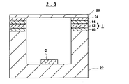
- FIG. 3 is a cross-sectional view of another embodiment of the electronic component storage package and the electronic device of the present invention.
- FIGS. 4 (1) to 4 (8) are views for explaining a method of joining a lid to a case containing an electronic component using a seal ring.
- FIG. 5A is a plan view showing two spots generated on a conventional metal layer
- FIG. 5B is an enlarged photograph (b) of the spots.
- FIG.1 (a) and FIG.1 (b) are sectional drawings for demonstrating one Embodiment of the seal ring of this invention.
- a seal ring 1 of the present invention has a nickel layer 14 on one surface of a base material 12 containing Kovar (iron-nickel-cobalt alloy) and a metal brazing material layer 16 on the other surface. And is formed in an annular shape.
- the surface having the nickel layer 14 of the base material 12 is referred to as a first surface
- the surface having the metal brazing material layer 16 is referred to as a second surface.
- a metal layer is provided on the upper surface of the nickel layer 14 on the first surface of the seal ring 1, and the metal layer is formed of nickel. Therefore, in order to distinguish this from the nickel layer 14, when the metal layer is made of nickel, it may be referred to as an upper nickel layer.
- the seal ring 1 of the present invention has a nickel layer 14 on the first surface of a base material 12 containing kovar (iron-nickel-cobalt alloy). Since the coefficient of thermal expansion of Kovar is close to the coefficient of thermal expansion of ceramics etc. in the package for storing electronic components, cracks will occur even when the ceramic ring and the seal ring are heated and then cooled. Can be suppressed.
- kovar iron-nickel-cobalt alloy
- kovar is mixed with silicon oxide, aluminum oxide and / or manganese sulfide as inevitable impurities in the production process, and the total of inevitable impurities in kovar is usually 1.5% or less, typically Specifically, it is 0.3% to 0.8%.
- the thickness of the base material 12 may be set as appropriate depending on the size and application of the electronic component storage package that is the final product.
- the thickness after the rolling process is, for example, 0.1 mm to 20 mm, 0.3 mm to 3 mm is preferable.
- the component ratio of Kovar's iron, nickel, cobalt and inevitable impurities used for the base material 12 is not particularly limited, and the coefficient of thermal expansion of Kovar is the heat of a case such as a ceramic of a package for storing electronic components. What is necessary is just to employ
- the thickness of the nickel layer 14 needs to be 0.1 ⁇ m to 20 ⁇ m as the thickness after the rolling treatment.
- the thickness is less than 0.1 ⁇ m, the layer is too thin to prevent the occurrence of spots on the metal layer surface.
- thermal expansion increases, which is not preferable.
- the film becomes too thick, peeling or warping of the film occurs due to the influence of internal stress in the film. Further, it is not preferable from the viewpoint of productivity and cost.
- the thickness of the nickel layer 14 after the rolling treatment is preferably 0.1 ⁇ m to 5 ⁇ m, more preferably 0.2 ⁇ m to 2 ⁇ m.
- the thickness of the nickel layer 14 after the rolling treatment is 0.1% to 1% with respect to the thickness of the base material 12 from the viewpoint of the difference between the surface covering effect and the thermal expansion coefficient. Is more preferable, and 0.2% to 0.5% is more preferable. If it is 0.1% or more, the effect of preventing the occurrence of spots on the metal layer surface is sufficiently obtained. If it is 1% or less, problems due to thermal stress are unlikely to occur, and cracking is unlikely to occur when cooled, which is preferable.
- the seal ring 1 of the present invention has a metal brazing material layer 16 on the second surface of the base material 12 containing Kovar (iron-nickel-cobalt alloy).
- Examples of the metal brazing material layer 16 include gold alloys such as Au—Sn, Au—Si, Au—Ge, Au—Cu, and Au—Ge—Ni, and silver alloys such as Ag—Cu, Examples thereof include Ag—Sn, Ag—Cu—Sn—In, and Ag—Cu—In. Among them, a silver alloy is preferable, and Ag—Cu is more preferable.
- the thickness of the metal brazing material layer 16 is, for example, 5 ⁇ m to 100 ⁇ m, preferably 10 ⁇ m to 40 ⁇ m, after the rolling treatment.
- the production method includes the following steps (1) to (3).
- the method of providing the nickel layer 14 on the first surface of the base material 12 is not particularly limited.
- a method of forming by the electroplating method a clad material is formed by press-contacting a nickel plate material. And a method of attaching a nickel foil.
- the method of providing the metal brazing material layer 16 on the second surface of the base material 12 is not particularly limited, but a method of forming a clad material by press-contacting a plate material made of a metal brazing material, It is preferable for the reason of improved bondability.
- the nickel layer 14 is also formed on the second surface of the base material 12 as shown in FIG. Will be provided. That is, the nickel layer 14 is formed between the second surface of the base material 12 and the metal brazing material layer 16. According to this form, the effect that the bondability between the brazing material and the base material is enhanced is exhibited.
- the base material 12 provided with the nickel layer 14 and the metal brazing material layer 16 is rolled.
- the rolling treatment include a known cold rolling treatment using a roll, and the rolling reduction is, for example, 30% or more, preferably 40 to 80%. By setting the rolling reduction in the above range, it is possible to prevent a stain on the surface of the metal layer while the nickel layer is thinner.
- the base material 12 before the rolling treatment is preferably subjected to a heat treatment at 500 ° C. or more, preferably 600 ° C. to 800 ° C., for the reason of improving the adhesion of the nickel layer 14 and the rolling processability.
- annular seal ring 1 having a desired size can be obtained by applying known means such as a press process to the base material 12 after the rolling process.
- FIG. 2 is a cross-sectional view of an embodiment of the electronic component storage package and the electronic device of the present invention.
- the electronic component storage package 2 of the present invention includes the seal ring 1 made of the base material 12, the nickel layer 14, and the metal brazing material layer 16 obtained as described above, and the electronic component in which the electronic component C is accommodated.
- a housing case 22 is joined via a metal brazing material layer 16, a metal layer 24 is provided on the upper surface of the nickel layer 14, and a lid 26 is joined on the metal layer 24.
- Examples of the electronic component C include piezoelectric components such as SAW filters and crystal resonators, semiconductor components such as semiconductor integrated circuit elements and optical semiconductor elements, and sensor components. Further, the electronic component C housed in the electronic component housing case 22 is hermetically sealed in a container (not shown) formed by the electronic component housing case 22 and the lid body 26 joined to each other, and the crystal An electronic device 3 such as a device is configured.
- the electronic component storage case 22 is not particularly limited, and a conventionally known aluminum oxide or ceramic such as aluminum nitride can be used.
- Examples of the metal layer 24 include a nickel layer (upper nickel layer) and a gold layer.
- Examples of the method of forming the metal layer 24 include a method of forming by an electroplating method, and a method of attaching a metal foil constituting the metal layer 24 onto the nickel layer 14.
- the thickness of the metal layer 24 is preferably 1 ⁇ m to 10 ⁇ m, more preferably 2 ⁇ m to 5 ⁇ m.
- a gold layer 244 may be further provided on the upper nickel layer 242 as the metal layer 24. According to this form, the airtightness with the lid body 26 is further improved, which is preferable.
- the lid 26 can be made of a low thermal expansion metal such as Kovar or iron-nickel alloy.
- the electronic component C hermetically sealed in a container between the lid 26 and the electronic component storage case 22 is provided on the surface and inside of the electronic component storage case 22, for example.
- the wiring conductor (not shown) is electrically connected to the external electric circuit.
- the wiring conductor is provided from the surface of the electronic component storage case 22 in the container (such as the bottom surface of the concave portion) to the outer surface such as the lower surface or the outer surface of the electronic component storage case 22.
- the electronic component C is electrically connected to a portion of the wiring conductor provided in the container by a conductive connecting material (not shown) such as a bonding wire, and the outer surface of the electronic component storage case of the wiring conductor.
- the part provided in the electric circuit is electrically connected to the external electric circuit by a conductive connecting material (not shown) such as a low melting point brazing material, and the hermetically sealed electronic component C and the external electric circuit are electrically connected to each other.
- the external electric circuit is a circuit board provided in an electronic device such as a mobile phone (so-called smartphone or the like), a computer, a device for image processing such as imaging, and a sensor device of various physical quantities such as acceleration.
- the electronic component storage package 2 of the present invention includes the seal ring 1 including the base material 12, the nickel layer 14, and the metal brazing material layer 16, and the electronic component storage case 22 that stores the electronic component C therein.
- the metal layer 24 is provided on the upper surface of the nickel layer 14, whereby the electronic component housing package 2 can be manufactured.
- the electronic device 3 can be manufactured by bonding the lid 26 on the metal layer 24.
- the electronic component C may be accommodated after the metal layer 24 is provided on the upper surface of the nickel layer 14.
- the manufacturing method of the electronic device 3 of the present invention includes the steps of preparing the electronic component storage package 2, the lid 26 and the electronic component C, and the step of storing the electronic component C in the electronic component storage case 22. And bonding the lid 26 on the metal layer 24.
- Examples of a method for joining the seal ring 1 and the electronic component storage case 22 include a brazing method using a brazing material such as silver brazing, and examples of a method for joining the metal layer 24 and the lid 26 include parallel.
- the method of seam welding is mentioned.
- a metallizing layer such as tungsten or molybdenum serving as a base metal for brazing and a brazing metal layer such as a nickel plating layer thereon are provided on the upper surface of the electronic component storage case 22. It has been.
- Example 1 Kovar plate material (iron-29 mass% nickel, containing 0.09% silicon oxide in silicon, 0.01% aluminum oxide in aluminum, 0.34% manganese sulfide in manganese) Nickel plating was performed on the first surface and the second surface of the base material 12 made of 17 mass% cobalt, width 20 mm, and length 100 m by an electroplating method, and the nickel layer 14 was provided. Next, a plate material (width 20 mm, length 100 m) made of a silver-28 mass% copper alloy as a metal brazing material is pressed against the second surface, a metal brazing material layer 16 is provided, and the reduction rate is baked at 600 ° C. for 3 minutes. The seal ring material was manufactured by rolling at 60%.
- the seal ring 1 was manufactured by punching from the second surface provided with the metal brazing filler metal. Table 1 shows the thickness of each layer of the obtained seal ring 1.
- Example 2 Example 1 was repeated except that the thickness of each layer was changed as shown in Table 1. The results are shown in Table 1.
- Example 1 was repeated except that the nickel layer 14 was not provided and the thickness of each layer was changed as shown in Table 1. The results are shown in Table 1.
Landscapes
- Physics & Mathematics (AREA)
- Acoustics & Sound (AREA)
- Piezo-Electric Or Mechanical Vibrators, Or Delay Or Filter Circuits (AREA)
- Engineering & Computer Science (AREA)
- Manufacturing & Machinery (AREA)
Abstract
本発明は、コバールを含むベース材の片面に金属ろう材層を有し、他面に金属鍍金層を有するシールリングにおいて、金属鍍金層表面へのシミの発生を防止し、電子部品収納用パッケージの優れた気密性を達成できるシールリングを提供することを課題とする。本発明は、コバール(鉄-ニッケル-コバルト合金)を含むベース材の第1面にニッケル層を有し、前記第1面の反対側の第2面に金属ろう材層を有してなる、環状のシールリングであって、前記ニッケル層の厚さが、0.1μm~20μmであるシールリングによって、上記課題を解決した。
Description
本発明は、シールリング、電子部品収納用パッケージ、電子デバイスおよびこれらの製造方法に関する。
携帯電話等の電子機器で使用されるSAWフィルタ、水晶振動子のような電子部品は、そのような電子部品を、開口を有するケースに収容し、これに蓋体を被せて封止したパッケージとして用いられている。パッケージを封止するのは、電子部品が空気中の湿気、酸素により特性が不安定となるのを防止するためである。
この電子部品のパッケージにおいて、ケースはアルミナ、窒化アルミニウム等のセラミック製のものが一般的であり、蓋体はコバール(鉄-ニッケル-コバルト合金(KOVAR:米国登録商標シリアルNo.71367381))、鉄-ニッケル合金等の低熱膨張金属よりなる。
蓋体のケースへの接合方法としては、蓋体となる基材に予め、ろう材を接合したクラッド材の状態のものを利用して、接合を行う方法がある(例えば、特許文献1参照)。これとは別に、前記のセラミック製のケースの上に、ろう材をクラッドしたコバール等の金属からなる枠状のシールリングを設け、このシールリングの上面に蓋体を接合するという方法もある(例えば、特許文献2参照)。
図4は、シールリングを用いて電子部品を収容したケースに蓋体を接合する方法を説明するための図である。
図4において、まず(1)コバール402および金属ろう材404を準備し、(2)これらをはり合わせ、クラッド材40にし、(3)圧延加工する。(4)圧延加工されたクラッド材40をリング状にプレス加工する。続いて、(5)電子部品を収容したセラミック製のケース46を準備し、(6)金属ろう材404とケース46とが接するように、シーム溶接する。その後、(7)シールリングのコバール402の上面にニッケルや金のような金属層48を設け、(8)金属層48上に蓋体49を接合する。
しかしながら、従来のシールリングを用いると、金属層48の上面にシミが発生するという現象が見られる。図5(a)は、従来の金属層48上に発生した2箇所のシミを示す平面の図であり、図5(b)はその拡大写真である。図5(a)及び図5(b)に示すようなシミは金属層48のボイドに相当し、シールリングと蓋体49との気密性を悪化させてしまうという大きな問題点がある。
したがって本発明の目的は、シールリング上に設けられる金属層表面へのシミの発生を防止し、電子部品収納用パッケージの優れた気密性を達成できるシールリング、これを用いた電子部品収納用パッケージ、電子デバイスおよびこれらの製造方法を提供することにある。
本発明者らは鋭意研究を重ねた結果、圧延処理を施す前のベース材の一方の面(金属ろう材層が設けられる面とは反対の面)にニッケル層を設け、圧延処理後の該ニッケル層の厚さを所定の範囲に規定することにより、上記のような従来の課題を解決できることを見出し、本発明を完成することができた。
したがって本発明は、以下の通りである。
1.コバール(鉄-ニッケル-コバルト合金)を含むベース材の第1面にニッケル層を有し、前記第1面の反対側の第2面に金属ろう材層を有してなる、環状のシールリングであって、前記ニッケル層の厚さが、0.1μm~20μmであるシールリング。
2.前記第2面と前記金属ろう材層との間にニッケル層を有する前項1に記載のシールリング。
3.前記ベース材が、酸化ケイ素、酸化アルミニウムおよび硫化マンガンからなる群より選ばれる少なくとも1種を含有する前項1または2に記載のシールリング。
4.前記圧延処理後において、前記第1面の前記ニッケル層の厚さが前記ベース材の厚さに対して0.1%~1%である前項1~3のいずれか1項に記載のシールリング。
5.コバール(鉄-ニッケル-コバルト合金)を含むベース材の第1面にニッケル層が設けられるとともに、前記第1面の反対側の第2面に金属ろう材層が設けられ、前記ベース材に対して、圧延処理が施されて、環状に形成されたシールリングであって、前記圧延処理後の前記ニッケル層の厚さが、0.1μm~20μmであるシールリング。
6.圧下率が30%以上の前記圧延処理を行うことで得られる前項5に記載のシールリング。
7.前記圧延処理前に500℃以上の熱処理を行うことで得られる前項5または6に記載のシールリング。
8.以下の工程(1)~(3)を含むシールリングの製造方法。
(1)コバール(鉄-ニッケル-コバルト合金)を含むベース材の第1面に、ニッケル層を設ける工程。
(2)前記第1面の反対側の第2面に、金属ろう材層を設ける工程。
(3)前記ニッケル層および前記金属ろう材層が設けられた前記ベース材を圧延する工程。
9.前記ニッケル層の厚さが、0.1μm~20μmである、前項8に記載のシールリングの製造方法。
10.前記圧延を圧下率が30%以上で行う、前項8または9に記載のシールリングの製造方法。
11.前記圧延前に500℃以上の熱処理を行う、前項8~10のいずれか1項に記載のシールリングの製造方法。
12.前項1~7のいずれか1項に記載のシールリングと、
前記金属ろう材層を介して前記第2面に設けられた電子部品収納用ケースとを有し、
前記第1面に設けられた前記ニッケル層の上面に金属層を有する電子部品収納用パッケージ。
13.前記金属層が、ニッケル層からなる前項12に記載の電子部品収納用パッケージ。
14.前記金属層は、前記ニッケル層の上面に、上部ニッケル層および金層がこの順で設けられたものである前項12に記載の電子部品収納用パッケージ。
15.前項1~7のいずれか1項に記載のシールリングと、電子部品収納用ケースとを、前記金属ろう材層を介して接合する工程と
前記第1面のニッケル層上に金属層を設ける工程とを含む電子部品収納用パッケージを製造する方法。
16.前項12~14のいずれか1項に記載の電子部品収納用パッケージと、
前記電子部品収納用ケース内に収容された電子部品と、
前記金属層上に接合された蓋体とを有する電子デバイス。
17.前項12~14のいずれか1項に記載の電子部品収納用パッケージ、蓋体および電子部品を準備する工程と、
前記電子部品収納用ケース内に前記電子部品を収容する工程と、
前記金属層上に前記蓋体を接合する工程とを含む電子デバイスを製造する方法。
1.コバール(鉄-ニッケル-コバルト合金)を含むベース材の第1面にニッケル層を有し、前記第1面の反対側の第2面に金属ろう材層を有してなる、環状のシールリングであって、前記ニッケル層の厚さが、0.1μm~20μmであるシールリング。
2.前記第2面と前記金属ろう材層との間にニッケル層を有する前項1に記載のシールリング。
3.前記ベース材が、酸化ケイ素、酸化アルミニウムおよび硫化マンガンからなる群より選ばれる少なくとも1種を含有する前項1または2に記載のシールリング。
4.前記圧延処理後において、前記第1面の前記ニッケル層の厚さが前記ベース材の厚さに対して0.1%~1%である前項1~3のいずれか1項に記載のシールリング。
5.コバール(鉄-ニッケル-コバルト合金)を含むベース材の第1面にニッケル層が設けられるとともに、前記第1面の反対側の第2面に金属ろう材層が設けられ、前記ベース材に対して、圧延処理が施されて、環状に形成されたシールリングであって、前記圧延処理後の前記ニッケル層の厚さが、0.1μm~20μmであるシールリング。
6.圧下率が30%以上の前記圧延処理を行うことで得られる前項5に記載のシールリング。
7.前記圧延処理前に500℃以上の熱処理を行うことで得られる前項5または6に記載のシールリング。
8.以下の工程(1)~(3)を含むシールリングの製造方法。
(1)コバール(鉄-ニッケル-コバルト合金)を含むベース材の第1面に、ニッケル層を設ける工程。
(2)前記第1面の反対側の第2面に、金属ろう材層を設ける工程。
(3)前記ニッケル層および前記金属ろう材層が設けられた前記ベース材を圧延する工程。
9.前記ニッケル層の厚さが、0.1μm~20μmである、前項8に記載のシールリングの製造方法。
10.前記圧延を圧下率が30%以上で行う、前項8または9に記載のシールリングの製造方法。
11.前記圧延前に500℃以上の熱処理を行う、前項8~10のいずれか1項に記載のシールリングの製造方法。
12.前項1~7のいずれか1項に記載のシールリングと、
前記金属ろう材層を介して前記第2面に設けられた電子部品収納用ケースとを有し、
前記第1面に設けられた前記ニッケル層の上面に金属層を有する電子部品収納用パッケージ。
13.前記金属層が、ニッケル層からなる前項12に記載の電子部品収納用パッケージ。
14.前記金属層は、前記ニッケル層の上面に、上部ニッケル層および金層がこの順で設けられたものである前項12に記載の電子部品収納用パッケージ。
15.前項1~7のいずれか1項に記載のシールリングと、電子部品収納用ケースとを、前記金属ろう材層を介して接合する工程と
前記第1面のニッケル層上に金属層を設ける工程とを含む電子部品収納用パッケージを製造する方法。
16.前項12~14のいずれか1項に記載の電子部品収納用パッケージと、
前記電子部品収納用ケース内に収容された電子部品と、
前記金属層上に接合された蓋体とを有する電子デバイス。
17.前項12~14のいずれか1項に記載の電子部品収納用パッケージ、蓋体および電子部品を準備する工程と、
前記電子部品収納用ケース内に前記電子部品を収容する工程と、
前記金属層上に前記蓋体を接合する工程とを含む電子デバイスを製造する方法。
本発明者らは、シールリング上の金属層の上面に発生するシミは、コバールの製造工程で不可避不純物として混入される酸化ケイ素、酸化アルミニウムおよび/または硫化マンガンが原因であることを突き止めた。これらの不純物は、圧延工程で引き伸ばされ、ベース材の表面、さらには金属層の表面にシミとなって浮き出てしまい、ボイドとなってシールリングと蓋体との気密性を悪化させてしまう。
そこで本発明では、圧延処理を施す前のベース材の一方の面(金属ろう材層が設けられる面とは反対の面)にニッケル層を設け、圧延処理後の該ニッケル層の厚さを所定の範囲に規定することにより、圧延工程で引き伸ばされた不純物が該ニッケル層に遮られ、金属層の表面に浮き出ることを抑制し、これによりシミの発生を防止することができ、結果としてシールリングと蓋体との優れた気密性を提供することを可能にした。
以下、本発明の実施形態について、さらに詳細に説明する。
図1(a)及び図1(b)は、本発明のシールリングの一実施形態を説明するための断面図である。
図1(a)及び図1(b)は、本発明のシールリングの一実施形態を説明するための断面図である。
図1(a)において、本発明のシールリング1は、コバール(鉄-ニッケル-コバルト合金)を含むベース材12の一方の面にニッケル層14を有し、他方の面に金属ろう材層16を有し、環状に形成されている。本明細書では、ベース材12のニッケル層14を有する面を第1面と呼び、金属ろう材層16を有する面を第2面と呼ぶ。
また、下記で説明するように、電子部品収納用パッケージを製造する際には、シールリング1の第1面におけるニッケル層14の上面に、金属層を有し、この金属層はニッケルからなる形態が含まれるため、これとニッケル層14とを区別することを目的として、金属層がニッケルからなる場合は、これを上部ニッケル層と呼ぶこともある。
以下、シールリングの各層について説明する。
本発明のシールリング1は、コバール(鉄-ニッケル-コバルト合金)を含むベース材12の第1面にニッケル層14を有する。コバールの熱膨張率は、電子部品収納用のパッケージのセラミック等の熱膨張率に近いため、セラミック等とシールリングを接合する際に熱をかけた後、冷却した場合であっても割れの発生を抑えることができる。
本発明のシールリング1は、コバール(鉄-ニッケル-コバルト合金)を含むベース材12の第1面にニッケル層14を有する。コバールの熱膨張率は、電子部品収納用のパッケージのセラミック等の熱膨張率に近いため、セラミック等とシールリングを接合する際に熱をかけた後、冷却した場合であっても割れの発生を抑えることができる。
また、上述のようにコバールには、その製造工程における不可避不純物として、酸化ケイ素、酸化アルミニウムおよび/または硫化マンガンが混入され、通常、コバール中の該不可避不純物の合計は1.5%以下、典型的には0.3%~0.8%である。
ベース材12の厚さは、最終製品である電子部品収納用パッケージのサイズや用途により適宜設定すればよいが、圧延処理を施した後の厚さとして、例えば、0.1mm~20mmであり、0.3mm~3mmが好ましい。
また、ベース材12に用いられるコバールの鉄、ニッケル、コバルトおよび不可避不純物の成分比は、特に限定するものではなく、コバールの熱膨張係数が、電子部品収納用のパッケージのセラミック等のケースの熱膨張係数に揃うように適宜成分比のものを採用すればよい。
また、ニッケル層14の厚さは、圧延処理を施した後の厚さとして、0.1μm~20μmであることが必要である。0.1μm未満であると、層が薄すぎて金属層表面のシミの発生を防止することができない。逆に20μmを超えると、熱膨張が大きくなり好ましくない。また、膜が厚くなりすぎると、膜中の内部応力の影響により、膜の剥がれや反りが発生してしまう。また、生産性やコスト面からも好ましくない。圧延処理を施した後のニッケル層14の厚さは、0.1μm~5μmが好ましく、0.2μm~2μmがさらに好ましい。
なお、圧延処理を施した後のニッケル層14の厚さは、表面の被覆効果と熱膨張率の差という観点から、ベース材12の厚さに対して0.1%~1%であるのが好ましく、0.2%~0.5%であるのがさらに好ましい。0.1%以上であれば、金属層表面のシミの発生の防止の効果が十分得られる。1%以下であれば、熱応力による不具合が生じにくく、冷却された際に割れが生じにくいため好ましい。
また、本発明のシールリング1は、コバール(鉄-ニッケル-コバルト合金)を含むベース材12の第2面に金属ろう材層16を有する。
金属ろう材層16としては、金合金として、例えば、Au-Sn、Au-Si、Au-Ge、Au-CuおよびAu-Ge-Ni等が挙げられ、銀合金として、例えば、Ag-Cu、Ag-Sn、Ag-Cu-Sn-InおよびAg-Cu-In等が挙げられ、中でも銀合金が好ましく、Ag-Cuがより好ましい。
金属ろう材層16の厚さは、圧延処理を施した後の厚さとして、例えば5μm~100μmであり、10μm~40μmが好ましい。
次に、本発明のシールリングの製造方法について説明する。該製造方法は、以下の工程(1)~(3)を含む。
(1)コバール(鉄-ニッケル-コバルト合金)を含むベース材12の第1面に、ニッケル層14を設ける工程。
(2)前記第1面の反対側の第2面に、金属ろう材層16を設ける工程。
(3)前記ニッケル層14および金属ろう材層16が設けられた前記ベース材12を圧延する工程。
(1)コバール(鉄-ニッケル-コバルト合金)を含むベース材12の第1面に、ニッケル層14を設ける工程。
(2)前記第1面の反対側の第2面に、金属ろう材層16を設ける工程。
(3)前記ニッケル層14および金属ろう材層16が設けられた前記ベース材12を圧延する工程。
前記(1)工程において、ベース材12の第1面にニッケル層14を設ける方法としては、とくに制限されず、例えば電気鍍金法により形成する方法、ニッケル製の板材を圧接してクラッド材を形成する方法、ニッケル製の箔をはり付ける方法等が挙げられる。
また前記(2)工程において、ベース材12の第2面に金属ろう材層16を設ける方法としては、とくに制限されないが、金属ろう材からなる板材を圧接してクラッド材を形成する方法が、接合性向上という理由から好ましい。
なお、ベース材12の第1面へのニッケル層14の形成方法として電気鍍金法が採用された場合は、図1(b)に示すように、ベース材12の第2面にもニッケル層14が設けられることになる。すなわち、ベース材12の第2面と金属ろう材層16との間には、ニッケル層14が形成される。この形態によれば、ろう材とベース材との接合性が高くなるという効果が奏される。
続いて前記(3)工程において、ニッケル層14および金属ろう材層16が設けられたベース材12を圧延する。圧延処理としては、例えばロールを用いた公知の冷間圧延処理が挙げられ、圧下率は例えば30%以上であり、40~80%が好ましい。圧下率を上記範囲にすることで、ニッケル層がより薄い状態で、金属層表面のシミを防ぐことができる。
圧延処理前のベース材12は、ニッケル層14の密着性および圧延加工性向上という理由から、500℃以上、好ましくは600℃~800℃の熱処理を施すことが好ましい。
続いて、圧延処理後のベース材12に対し、プレス処理等の公知の手段を施すことにより、所望のサイズの環状のシールリング1を得ることができる。
次に本発明の電子部品収納用パッケージおよび電子デバイスについて説明する。
図2は、本発明の電子部品収納用パッケージおよび電子デバイスの一実施形態の断面図である。
本発明の電子部品収納用パッケージ2は、上記のようにして得られた、ベース材12、ニッケル層14および金属ろう材層16からなるシールリング1と、内部に電子部品Cを収容した電子部品収納用ケース22とが、金属ろう材層16を介して接合され、ニッケル層14の上面には金属層24が設けられ、金属層24上に蓋体26が接合され、構成されている。
図2は、本発明の電子部品収納用パッケージおよび電子デバイスの一実施形態の断面図である。
本発明の電子部品収納用パッケージ2は、上記のようにして得られた、ベース材12、ニッケル層14および金属ろう材層16からなるシールリング1と、内部に電子部品Cを収容した電子部品収納用ケース22とが、金属ろう材層16を介して接合され、ニッケル層14の上面には金属層24が設けられ、金属層24上に蓋体26が接合され、構成されている。
電子部品Cとしては、例えばSAWフィルタおよび水晶振動子等の圧電部品、半導体集積回路素子および光半導体素子等の半導体部品、ならびにセンサ部品等が挙げられる。また、電子部品収納用ケース22内に収容された電子部品Cが、互いに接合された電子部品収納用ケース22および蓋体26によって形成される容器(符号なし)内に気密封止されて、水晶デバイス等の電子デバイス3が構成されている。
電子部品収納用ケース22としては、特に制限されず、従来公知の酸化アルミニウムや、窒化アルミニウム等のセラミック製のものを使用することができる。
金属層24としては、例えばニッケル層(上部ニッケル層)、金層等が挙げられる。
金属層24の形成方法としては、例えば電気鍍金法により形成する方法、金属層24を構成する金属の箔をニッケル層14上にはり付ける方法等が挙げられる。
金属層24の厚さは、1μm~10μmが好ましく、2μm~5μmがより好ましい。
金属層24の形成方法としては、例えば電気鍍金法により形成する方法、金属層24を構成する金属の箔をニッケル層14上にはり付ける方法等が挙げられる。
金属層24の厚さは、1μm~10μmが好ましく、2μm~5μmがより好ましい。
また、図3に示すように、金属層24として、上部ニッケル層242上に、金層244をさらに設けてもよい。この形態によれば、蓋体26との気密性がさらに向上し、好ましい。
蓋体26は、コバールや鉄-ニッケル合金等の低熱膨張金属を使用することができる。なお、電子デバイス3について、この蓋体26および電子部品収納用ケース22との間の容器に気密封止されている電子部品Cは、例えば、電子部品収納用ケース22の表面および内部に設けられた配線導体(図示せず)によって、外部電気回路に電気的に接続される。この場合の配線導体は、容器内における電子部品収納用ケース22の表面(凹部分の底面等)から電子部品収納用ケース22の下面または外側面等の外表面にかけて設けられる。
配線導体のうち容器内に設けられた部分に電子部品Cがボンディングワイヤ等の導電性接続材(図示せず)によって電気的に接続されるとともに、配線導体のうち電子部品収納用ケースの外表面に設けられた部分が外部電気回路に低融点ろう材等の導電性接続材(図示せず)によって電気的に接続されて、気密封止された電子部品Cと外部電気回路とが互いに電気的に接続される。外部電気回路は、例えば、携帯電話(いわゆるスマートフォン等)、コンピュータ、撮像等の画像処理用の機器および加速度等の各種の物理量のセンサ機器等の電子機器が備える回路基板である。
次に本発明の電子部品収納用パッケージおよび電子デバイスの製造方法について説明する。
上記のように本発明の電子部品収納用パッケージ2は、ベース材12、ニッケル層14および金属ろう材層16からなるシールリング1と、内部に電子部品Cを収容した電子部品収納用ケース22とを、金属ろう材層16を介して接合し、ニッケル層14の上面に金属層24を設けることによって電子部品収納用パッケージ2を製造することができる。また、最後に金属層24上に蓋体26を接合することにより電子デバイス3を製造することができる。電子部品Cの収容は、ニッケル層14の上面に金属層24を設けた後で行ってもよい。すなわち、本発明の電子デバイス3の製造方法は、上記電子部品収納用パッケージ2、蓋体26および電子部品Cを準備する工程と、電子部品収納用ケース22内に電子部品Cを収容する工程と、金属層24上に蓋体26を接合する工程とを含む。
上記のように本発明の電子部品収納用パッケージ2は、ベース材12、ニッケル層14および金属ろう材層16からなるシールリング1と、内部に電子部品Cを収容した電子部品収納用ケース22とを、金属ろう材層16を介して接合し、ニッケル層14の上面に金属層24を設けることによって電子部品収納用パッケージ2を製造することができる。また、最後に金属層24上に蓋体26を接合することにより電子デバイス3を製造することができる。電子部品Cの収容は、ニッケル層14の上面に金属層24を設けた後で行ってもよい。すなわち、本発明の電子デバイス3の製造方法は、上記電子部品収納用パッケージ2、蓋体26および電子部品Cを準備する工程と、電子部品収納用ケース22内に電子部品Cを収容する工程と、金属層24上に蓋体26を接合する工程とを含む。
シールリング1と電子部品収納用ケース22との接合方法としては、例えば、銀ろう等のろう材によるろう付け法が挙げられ、金属層24と蓋体26との接合方法としては、例えば、パラレルシーム溶接する方法が挙げられる。なお、電子部品収納用ケース22の上面には、図示していないが、ろう付け用の下地金属となるタングステンやモリブデン等のメタライズ層およびその上のニッケル鍍金層等のろう付け用金属層が設けられている。
以下、本発明を実施例によりさらに説明するが、本発明は下記例に制限されるものではない。
実施例1
コバール製の板材(合金中にケイ素量で0.09%の酸化ケイ素、アルミニウム量で0.01%の酸化アルミニウム、マンガン量で0.34%の硫化マンガンを含む、鉄-29質量%ニッケル-17質量%コバルト、幅20mm、長さ100m)からなるベース材12の第1面および第2面に電気鍍金法によりニッケル鍍金を行い、ニッケル層14をそれぞれ設けた。ついで、金属ろう材として銀-28質量%銅合金からなる板材(幅20mm、長さ100m)を第2面に圧接し、金属ろう材層16を設け、600℃で3分間焼成して圧下率60%で圧延し、シールリング材を製造した。
コバール製の板材(合金中にケイ素量で0.09%の酸化ケイ素、アルミニウム量で0.01%の酸化アルミニウム、マンガン量で0.34%の硫化マンガンを含む、鉄-29質量%ニッケル-17質量%コバルト、幅20mm、長さ100m)からなるベース材12の第1面および第2面に電気鍍金法によりニッケル鍍金を行い、ニッケル層14をそれぞれ設けた。ついで、金属ろう材として銀-28質量%銅合金からなる板材(幅20mm、長さ100m)を第2面に圧接し、金属ろう材層16を設け、600℃で3分間焼成して圧下率60%で圧延し、シールリング材を製造した。
シールリング材の金属ろう材を設けた第2面から打ち抜き加工しシールリング1を製造した。得られたシールリング1の各層の厚さを表1に示す。
得られたシールリング1のニッケル層14上に、厚さ3μmとなるように電気ニッケル鍍金を施し、金属層24としての上部ニッケル層242を設けた。さらに、上部ニッケル層242上に金鍍金を施して金層244を設け、その金層244の上面シミの発生個数(個数/mm2)を、200倍率の光学顕微鏡で観察した。該シミの発生率は、製造品10000個を観察し、シミの発生した製造品の個数から算出した値である。
結果を表1に示す。
結果を表1に示す。
実施例2
各層の厚さを表1に示すように変更したこと以外は、実施例1を繰り返した。
結果を表1に示す。
各層の厚さを表1に示すように変更したこと以外は、実施例1を繰り返した。
結果を表1に示す。
比較例1~3
ニッケル層14を設けずに、かつ、各層の厚さを表1に示すように変更したこと以外は、実施例1を繰り返した。
結果を表1に示す。
ニッケル層14を設けずに、かつ、各層の厚さを表1に示すように変更したこと以外は、実施例1を繰り返した。
結果を表1に示す。

表1の結果から、各実施例のシールリングは、ベース材の第1面にニッケル層14が所定の厚さで設けられているので、金属層24上のシミの発生が抑制され、電子部品収納用パッケージの優れた気密性を提供できることが判明した。
これに対し各比較例のシールリングは、ベース材の第1面にニッケル層14を設けていないので、金属層24上にシミが発生し、電子部品収納用パッケージの気密性に対し悪影響を及ぼすことが分かった。
本発明を特定の態様を用いて詳細に説明したが、本発明の意図と範囲を離れることなく様々な変更及び変形が可能であることは、当業者にとって明らかである。なお本出願は、2015年12月22日付で出願された日本特許出願(特願2015-250472)に基づいており、その全体が引用により援用される。
1 シールリング
12 ベース材
14 ニッケル層
16 金属ろう材層
2 電子部品収納用パッケージ
22 電子部品収納用ケース
24 金属層
242 上部ニッケル層
244 金層
26 蓋体
3 電子デバイス
40 クラッド材
402 コバール
404 金属ろう材
46 ケース
48 金属層
49 蓋体
C 電子部品
12 ベース材
14 ニッケル層
16 金属ろう材層
2 電子部品収納用パッケージ
22 電子部品収納用ケース
24 金属層
242 上部ニッケル層
244 金層
26 蓋体
3 電子デバイス
40 クラッド材
402 コバール
404 金属ろう材
46 ケース
48 金属層
49 蓋体
C 電子部品
Claims (17)
- コバール(鉄-ニッケル-コバルト合金)を含むベース材の第1面にニッケル層を有し、前記第1面の反対側の第2面に金属ろう材層を有してなる、環状のシールリングであって、前記ニッケル層の厚さが、0.1μm~20μmであるシールリング。
- 前記第2面と前記金属ろう材層との間にニッケル層を有する請求項1に記載のシールリング。
- 前記ベース材が、酸化ケイ素、酸化アルミニウムおよび硫化マンガンからなる群より選ばれる少なくとも1種を含有する請求項1または2に記載のシールリング。
- 前記圧延処理後において、前記第1面の前記ニッケル層の厚さが前記ベース材の厚さに対して0.1%~1%である請求項1~3のいずれか1項に記載のシールリング。
- コバール(鉄-ニッケル-コバルト合金)を含むベース材の第1面にニッケル層が設けられるとともに、前記第1面の反対側の第2面に金属ろう材層が設けられ、前記ベース材に対して、圧延処理が施されて、環状に形成されたシールリングであって、前記圧延処理後の前記ニッケル層の厚さが、0.1μm~20μmであるシールリング。
- 圧下率が30%以上の前記圧延処理を行うことで得られる請求項5に記載のシールリング。
- 前記圧延処理前に500℃以上の熱処理を行うことで得られる請求項5または6に記載のシールリング。
- 以下の工程(1)~(3)を含むシールリングの製造方法。
(1)コバール(鉄-ニッケル-コバルト合金)を含むベース材の第1面に、ニッケル層を設ける工程。
(2)前記第1面の反対側の第2面に、金属ろう材層を設ける工程。
(3)前記ニッケル層および前記金属ろう材層が設けられた前記ベース材を圧延する工程。 - 前記ニッケル層の厚さが、0.1μm~20μmである、請求項8に記載のシールリングの製造方法。
- 前記圧延を圧下率が30%以上で行う、請求項8または9に記載のシールリングの製造方法。
- 前記圧延前に500℃以上の熱処理を行う、請求項8~10のいずれか1項に記載のシールリングの製造方法。
- 請求項1~7のいずれか1項に記載のシールリングと、
前記金属ろう材層を介して前記第2面に設けられた電子部品収納用ケースとを有し、
前記第1面に設けられた前記ニッケル層の上面に金属層を有する電子部品収納用パッケージ。 - 前記金属層が、ニッケル層からなる請求項12に記載の電子部品収納用パッケージ。
- 前記金属層は、前記ニッケル層の上面に、上部ニッケル層および金層がこの順で設けられたものである請求項12に記載の電子部品収納用パッケージ。
- 請求項1~7のいずれか1項に記載のシールリングと、電子部品収納用ケースとを、前記金属ろう材層を介して接合する工程と
前記第1面のニッケル層上に金属層を設ける工程とを含む電子部品収納用パッケージを製造する方法。 - 請求項12~14のいずれか1項に記載の電子部品収納用パッケージと、
前記電子部品収納用ケース内に収容された電子部品と、
前記金属層上に接合された蓋体とを有する電子デバイス。 - 請求項12~14のいずれか1項に記載の電子部品収納用パッケージ、蓋体および電子部品を準備する工程と、
前記電子部品収納用ケース内に前記電子部品を収容する工程と、
前記金属層上に前記蓋体を接合する工程とを含む電子デバイスを製造する方法。
Priority Applications (2)
| Application Number | Priority Date | Filing Date | Title |
|---|---|---|---|
| CN201680075196.8A CN108370244B (zh) | 2015-12-22 | 2016-12-19 | 密封环、电子元件收纳用封装体、电子设备及它们的制造方法 |
| US16/064,582 US10615090B2 (en) | 2015-12-22 | 2016-12-19 | Seal ring, electronic component housing package, electronic device, and manufacturing methods thereof |
Applications Claiming Priority (2)
| Application Number | Priority Date | Filing Date | Title |
|---|---|---|---|
| JP2015-250472 | 2015-12-22 | ||
| JP2015250472A JP6787662B2 (ja) | 2015-12-22 | 2015-12-22 | シールリング、電子部品収納用パッケージ、電子デバイスおよびこれらの製造方法 |
Publications (1)
| Publication Number | Publication Date |
|---|---|
| WO2017110728A1 true WO2017110728A1 (ja) | 2017-06-29 |
Family
ID=59090320
Family Applications (1)
| Application Number | Title | Priority Date | Filing Date |
|---|---|---|---|
| PCT/JP2016/087745 Ceased WO2017110728A1 (ja) | 2015-12-22 | 2016-12-19 | シールリング、電子部品収納用パッケージ、電子デバイスおよびこれらの製造方法 |
Country Status (5)
| Country | Link |
|---|---|
| US (1) | US10615090B2 (ja) |
| JP (1) | JP6787662B2 (ja) |
| CN (1) | CN108370244B (ja) |
| TW (1) | TWI662207B (ja) |
| WO (1) | WO2017110728A1 (ja) |
Families Citing this family (4)
| Publication number | Priority date | Publication date | Assignee | Title |
|---|---|---|---|---|
| CN108512523B (zh) * | 2017-11-06 | 2021-12-14 | 苏州汉天下电子有限公司 | 压电声波器件的封装方法及封装结构 |
| WO2019159858A1 (ja) * | 2018-02-13 | 2019-08-22 | 田中貴金属工業株式会社 | 透光性材料からなる封止用のリッド |
| US12394679B2 (en) * | 2019-09-30 | 2025-08-19 | Kyocera Corporation | Lid body, electronic component accommodation package, and electronic device |
| CN112382616A (zh) * | 2020-11-11 | 2021-02-19 | 合肥圣达电子科技实业有限公司 | 一种电子封装外壳及其制备方法 |
Citations (4)
| Publication number | Priority date | Publication date | Assignee | Title |
|---|---|---|---|---|
| JP2002030393A (ja) * | 2000-07-17 | 2002-01-31 | Hitachi Metals Ltd | セラミックパッケージ封止用材料とその製造方法 |
| JP2004063960A (ja) * | 2002-07-31 | 2004-02-26 | Kyocera Corp | 電子装置 |
| JP2009140784A (ja) * | 2007-12-07 | 2009-06-25 | Kanayama Seiki Co Ltd | 気密端子の製造方法 |
| JP2011119338A (ja) * | 2009-12-01 | 2011-06-16 | Misuzu Kogyo:Kk | 金属部材の接合方法、および接合金属部材ユニット |
Family Cites Families (17)
| Publication number | Priority date | Publication date | Assignee | Title |
|---|---|---|---|---|
| JPH0736952B2 (ja) * | 1986-11-27 | 1995-04-26 | 京セラ株式会社 | メタライズ金属層の表面被覆構造 |
| CN1056130A (zh) * | 1990-04-23 | 1991-11-13 | 上海钢铁研究所 | 耐腐蚀可伐合金 |
| US5498900A (en) * | 1993-12-22 | 1996-03-12 | Honeywell Inc. | Semiconductor package with weldable ceramic lid |
| JPH10247696A (ja) * | 1997-03-04 | 1998-09-14 | Sumitomo Kinzoku Electro Device:Kk | 半導体パッケージ気密封止用金属製蓋体 |
| JP3764669B2 (ja) * | 2001-10-25 | 2006-04-12 | 京セラ株式会社 | ろう材付きシールリングおよびこれを用いた電子部品収納用パッケージの製造方法 |
| JP2003158211A (ja) | 2001-11-19 | 2003-05-30 | Daishinku Corp | 電子部品用パッケージおよび当該パッケージを用いた圧電振動デバイス |
| US6627814B1 (en) * | 2002-03-22 | 2003-09-30 | David H. Stark | Hermetically sealed micro-device package with window |
| JP2006179614A (ja) * | 2004-12-21 | 2006-07-06 | Kyocera Corp | 電子部品 |
| JP4618790B2 (ja) * | 2005-04-07 | 2011-01-26 | 田中貴金属工業株式会社 | ハーメチックシールカバー及びその製造方法 |
| JP2010154191A (ja) * | 2008-12-25 | 2010-07-08 | Nippon Dempa Kogyo Co Ltd | 表面実装用の圧電デバイス |
| JP5923272B2 (ja) * | 2011-10-14 | 2016-05-24 | セイコーインスツル株式会社 | 電気化学セル、蓋体及び電気化学セルの製造方法 |
| JP6034054B2 (ja) * | 2012-04-27 | 2016-11-30 | 京セラ株式会社 | 電子部品収納用パッケージおよび電子装置 |
| CN203674191U (zh) * | 2013-12-19 | 2014-06-25 | 无锡微奇科技有限公司 | 传感器的真空陶瓷封装结构 |
| CN104726735B (zh) * | 2013-12-23 | 2017-02-08 | 北京有色金属研究总院 | 一种具有复合式结构的高定向导热材料及其制备方法 |
| CN103759864A (zh) * | 2014-01-26 | 2014-04-30 | 中国电子科技集团公司第四十九研究所 | 一种陶瓷封装结构及采用该陶瓷封装结构的压力敏感器件管壳 |
| CN103928409B (zh) * | 2014-03-17 | 2017-01-04 | 江苏省宜兴电子器件总厂 | 一种集成电路倒扣焊气密性封装结构 |
| JP6387818B2 (ja) * | 2014-12-11 | 2018-09-12 | 日立金属株式会社 | 気密封止用蓋材の製造方法 |
-
2015
- 2015-12-22 JP JP2015250472A patent/JP6787662B2/ja active Active
-
2016
- 2016-12-19 US US16/064,582 patent/US10615090B2/en active Active
- 2016-12-19 CN CN201680075196.8A patent/CN108370244B/zh active Active
- 2016-12-19 WO PCT/JP2016/087745 patent/WO2017110728A1/ja not_active Ceased
- 2016-12-22 TW TW105142739A patent/TWI662207B/zh active
Patent Citations (4)
| Publication number | Priority date | Publication date | Assignee | Title |
|---|---|---|---|---|
| JP2002030393A (ja) * | 2000-07-17 | 2002-01-31 | Hitachi Metals Ltd | セラミックパッケージ封止用材料とその製造方法 |
| JP2004063960A (ja) * | 2002-07-31 | 2004-02-26 | Kyocera Corp | 電子装置 |
| JP2009140784A (ja) * | 2007-12-07 | 2009-06-25 | Kanayama Seiki Co Ltd | 気密端子の製造方法 |
| JP2011119338A (ja) * | 2009-12-01 | 2011-06-16 | Misuzu Kogyo:Kk | 金属部材の接合方法、および接合金属部材ユニット |
Also Published As
| Publication number | Publication date |
|---|---|
| US10615090B2 (en) | 2020-04-07 |
| CN108370244B (zh) | 2021-12-24 |
| CN108370244A (zh) | 2018-08-03 |
| JP2017118272A (ja) | 2017-06-29 |
| TWI662207B (zh) | 2019-06-11 |
| JP6787662B2 (ja) | 2020-11-18 |
| US20180374767A1 (en) | 2018-12-27 |
| TW201736760A (zh) | 2017-10-16 |
Similar Documents
| Publication | Publication Date | Title |
|---|---|---|
| JP5795203B2 (ja) | 空洞筐体用の金属被覆及び非磁性密閉空洞筐体 | |
| US9859179B2 (en) | Lid body, package, and electronic apparatus | |
| KR101918877B1 (ko) | 기밀 밀봉용 덮개재, 기밀 밀봉용 덮개재의 제조 방법 및 전자 부품 수납 패키지 | |
| WO2017110728A1 (ja) | シールリング、電子部品収納用パッケージ、電子デバイスおよびこれらの製造方法 | |
| JP5680226B2 (ja) | 配線基板およびパッケージ、ならびに電子装置 | |
| JP2018142608A (ja) | 表面実装型電子部品 | |
| US10396002B2 (en) | Electronic component storage substrate and housing package | |
| JP5310309B2 (ja) | はんだコートリッド | |
| JP3706606B2 (ja) | 半導体素子収納用パッケージ | |
| JP3861280B2 (ja) | 気密封止型電子部品 | |
| JP7083898B2 (ja) | 基体および半導体装置 | |
| JP2005072421A (ja) | 電子部品収納用パッケージおよび電子装置 | |
| CN112750550A (zh) | 接合线以及半导体装置 | |
| JPWO2019208577A1 (ja) | 放熱基板および電子装置 | |
| JP2019076939A (ja) | ろう材、接合構造および半導体パッケージ | |
| JP4828980B2 (ja) | 接合部材及びその製造方法ならびに接合構造体及び基体の接続方法 | |
| JP6629660B2 (ja) | セラミックパッケージおよびその製造方法 | |
| JP3309045B2 (ja) | リード付き電子部品 | |
| JP6980415B2 (ja) | 電子部品収納用パッケージの製造方法および電子部品収納用パッケージ | |
| JP2007123465A (ja) | 電子部品収納用パッケージおよび電子装置およびその製造方法 | |
| JP2002184886A (ja) | はんだコートリッド | |
| JPS60123044A (ja) | 半導体装置 | |
| JPH0456343A (ja) | 半導体素子収納用パッケージ | |
| JP2003133460A (ja) | 気密封止型電子部品 | |
| JPH08227947A (ja) | 半導体素子収納用パッケージ |
Legal Events
| Date | Code | Title | Description |
|---|---|---|---|
| 121 | Ep: the epo has been informed by wipo that ep was designated in this application |
Ref document number: 16878617 Country of ref document: EP Kind code of ref document: A1 |
|
| NENP | Non-entry into the national phase |
Ref country code: DE |
|
| 122 | Ep: pct application non-entry in european phase |
Ref document number: 16878617 Country of ref document: EP Kind code of ref document: A1 |