WO2017110266A1 - 電力変換装置 - Google Patents
電力変換装置 Download PDFInfo
- Publication number
- WO2017110266A1 WO2017110266A1 PCT/JP2016/082866 JP2016082866W WO2017110266A1 WO 2017110266 A1 WO2017110266 A1 WO 2017110266A1 JP 2016082866 W JP2016082866 W JP 2016082866W WO 2017110266 A1 WO2017110266 A1 WO 2017110266A1
- Authority
- WO
- WIPO (PCT)
- Prior art keywords
- side branch
- negative side
- negative
- semiconductor element
- positive
- Prior art date
- Legal status (The legal status is an assumption and is not a legal conclusion. Google has not performed a legal analysis and makes no representation as to the accuracy of the status listed.)
- Ceased
Links
Images






Classifications
-
- H—ELECTRICITY
- H02—GENERATION; CONVERSION OR DISTRIBUTION OF ELECTRIC POWER
- H02M—APPARATUS FOR CONVERSION BETWEEN AC AND AC, BETWEEN AC AND DC, OR BETWEEN DC AND DC, AND FOR USE WITH MAINS OR SIMILAR POWER SUPPLY SYSTEMS; CONVERSION OF DC OR AC INPUT POWER INTO SURGE OUTPUT POWER; CONTROL OR REGULATION THEREOF
- H02M7/00—Conversion of AC power input into DC power output; Conversion of DC power input into AC power output
- H02M7/42—Conversion of DC power input into AC power output without possibility of reversal
- H02M7/44—Conversion of DC power input into AC power output without possibility of reversal by static converters
- H02M7/48—Conversion of DC power input into AC power output without possibility of reversal by static converters using discharge tubes with control electrode or semiconductor devices with control electrode
- H02M7/53—Conversion of DC power input into AC power output without possibility of reversal by static converters using discharge tubes with control electrode or semiconductor devices with control electrode using devices of a triode or transistor type requiring continuous application of a control signal
- H02M7/537—Conversion of DC power input into AC power output without possibility of reversal by static converters using discharge tubes with control electrode or semiconductor devices with control electrode using devices of a triode or transistor type requiring continuous application of a control signal using semiconductor devices only, e.g. single switched pulse inverters
- H02M7/5387—Conversion of DC power input into AC power output without possibility of reversal by static converters using discharge tubes with control electrode or semiconductor devices with control electrode using devices of a triode or transistor type requiring continuous application of a control signal using semiconductor devices only, e.g. single switched pulse inverters in a bridge configuration
-
- H—ELECTRICITY
- H02—GENERATION; CONVERSION OR DISTRIBUTION OF ELECTRIC POWER
- H02M—APPARATUS FOR CONVERSION BETWEEN AC AND AC, BETWEEN AC AND DC, OR BETWEEN DC AND DC, AND FOR USE WITH MAINS OR SIMILAR POWER SUPPLY SYSTEMS; CONVERSION OF DC OR AC INPUT POWER INTO SURGE OUTPUT POWER; CONTROL OR REGULATION THEREOF
- H02M7/00—Conversion of AC power input into DC power output; Conversion of DC power input into AC power output
- H02M7/003—Constructional details, e.g. physical layout, assembly, wiring or busbar connections
-
- H—ELECTRICITY
- H02—GENERATION; CONVERSION OR DISTRIBUTION OF ELECTRIC POWER
- H02P—CONTROL OR REGULATION OF ELECTRIC MOTORS, ELECTRIC GENERATORS OR DYNAMO-ELECTRIC CONVERTERS; CONTROLLING TRANSFORMERS, REACTORS OR CHOKE COILS
- H02P27/00—Arrangements or methods for the control of AC motors characterised by the kind of supply voltage
- H02P27/04—Arrangements or methods for the control of AC motors characterised by the kind of supply voltage using variable-frequency supply voltage, e.g. inverter or converter supply voltage
- H02P27/06—Arrangements or methods for the control of AC motors characterised by the kind of supply voltage using variable-frequency supply voltage, e.g. inverter or converter supply voltage using DC to AC converters or inverters
-
- H—ELECTRICITY
- H10—SEMICONDUCTOR DEVICES; ELECTRIC SOLID-STATE DEVICES NOT OTHERWISE PROVIDED FOR
- H10W—GENERIC PACKAGES, INTERCONNECTIONS, CONNECTORS OR OTHER CONSTRUCTIONAL DETAILS OF DEVICES COVERED BY CLASS H10
- H10W40/00—Arrangements for thermal protection or thermal control
- H10W40/20—Arrangements for cooling
- H10W40/22—Arrangements for cooling characterised by their shape, e.g. having conical or cylindrical projections
Definitions
- the present disclosure relates to a power conversion device including a plurality of semiconductor elements, a smoothing capacitor, and a positive bus bar and a negative bus bar that electrically connect them.
- a power conversion device such as an inverter or a DC-DC converter
- a device including a semiconductor element such as an IGBT, a smoothing capacitor, and a positive bus bar and a negative bus bar that electrically connect them is known (see Patent Document 1 below). ).
- the positive bus bar includes a positive main body portion connected to a capacitor and a plurality of positive branch portions extending from the positive main body portion and connected to the semiconductor element.
- the negative bus bar includes a negative main body portion connected to the capacitor and a plurality of negative side branch portions extending from the negative main body portion and connected to the semiconductor element.
- the positive side branch part and the negative side branch part are alternately arranged. Thereby, the positive side branch part and the negative side branch part are brought close to each other, and the parasitic inductance is reduced.
- the potentials of the reference electrodes such as the emitters (that is, the reference potentials) of the plurality of semiconductor elements that are electrically connected to the negative side branch portions and are simultaneously turned on / off are likely to be greatly different from each other. Therefore, as will be described later, there is a possibility that a high voltage is applied to the control terminals of some semiconductor elements.
- This disclosure is intended to provide a power conversion device that can reduce a difference in reference potentials of a plurality of semiconductor elements that are simultaneously turned on and off.
- a first aspect of the present disclosure includes a plurality of upper arm semiconductor elements and a lower arm semiconductor element that are connected in series to each other, Freewheeling diodes connected in reverse parallel to the individual semiconductor elements; A capacitor for smoothing the DC voltage; A positive bus bar having a positive main body electrically connected to the capacitor, and a plurality of positive branches extending from the positive main body and electrically connected to the upper arm semiconductor element; A negative bus bar having a negative main body electrically connected to the capacitor and a plurality of negative branches extending from the negative main body and electrically connected to the lower arm semiconductor element; The positive side branch part and the negative side branch part are alternately arranged, A semiconductor element group is formed which includes a plurality of the upper arm semiconductor elements that are simultaneously turned on and off, and a plurality of the lower arm semiconductor elements that are connected in series to the upper arm semiconductor elements and are simultaneously turned on and off, The negative side branch portion includes an intervening negative side branch interposed between the two positive side branch portions connected to the upper arm semiconductor element belonging to the same semiconductor element group as the lower
- the semiconductor element group is configured by a plurality of semiconductor elements that are alternately arranged on the positive side branch part and the negative side branch part and are connected to these branch parts and simultaneously turned on and off.
- the end negative side branch portion of the plurality of negative side branch portions has a smaller self-inductance than the intervening negative side branch portion. Therefore, the difference in reference potential among a plurality of semiconductor elements that are simultaneously turned on / off can be reduced. That is, since the end negative side branch is not interposed between the two positive side branches, as will be described later, than the intervening negative side branch interposed between the two positive side branches. Mutual inductance tends to increase.
- the end negative side branch portion where the mutual inductance tends to be large has a smaller self-inductance than the intervening negative side branch portion. Therefore, the difference in effective inductance (that is, a value obtained by adding mutual inductance and self-inductance) between the intervening negative branch and the end negative branch can be reduced. For this reason, the induced electromotive force generated due to the effective inductance when a current flows is unlikely to greatly differ between the intervening negative branch and the end negative branch. Therefore, it is possible to reduce the difference between the reference potential of the semiconductor element electrically connected to the intervening negative side branch and the reference potential of the semiconductor element electrically connected to the end negative side branch.
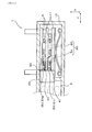
- FIG. 1 is a cross-sectional view of the power conversion device according to the first embodiment, and is a cross-sectional view taken along II in FIG.
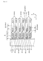
- FIG. 2 is a partially omitted cross-sectional view of the power conversion device according to the first embodiment.
- 3 is a cross-sectional view taken along the line III-III in FIG.
- FIG. 4 is a cross-sectional view of the power conversion apparatus with the positive bus bar removed in the first embodiment.
- FIG. 5 is a cross-sectional view of the power conversion apparatus according to the first embodiment from which the positive bus bar and the negative bus bar are removed.
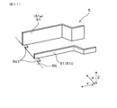
- FIG. 6 is an enlarged perspective view of a main part of the negative bus bar in the first embodiment.
- FIG. 7 is a circuit diagram of the power conversion device according to the first embodiment.
- FIG. 8 is a part of a circuit diagram of the power conversion device when the upper arm semiconductor element is turned off in the first embodiment.
- FIG. 9 is a part of a circuit diagram of the power conversion device when the upper arm semiconductor element is turned on in the first embodiment.
- FIG. 10 is a graph showing changes in the current flowing through the positive side branch and the negative side branch when the upper arm semiconductor element is switched from off to on in the first embodiment.
- FIG. 11 illustrates the reason why the difference in the reference potential of the upper arm semiconductor element can be reduced even when the upper arm semiconductor element and the lower arm semiconductor element are built in one semiconductor module in the first embodiment.
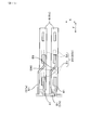
- FIG. 12 is a partially omitted cross-sectional view of the power conversion device according to the second embodiment.
- FIG. 13 is a cross-sectional view of the power conversion device according to the third embodiment.
- FIG. 14 is an enlarged cross-sectional view of a main part of the power conversion device according to the third embodiment.
- FIG. 15 is an enlarged cross-sectional view of a main part of the power conversion device according to the fourth embodiment.
- FIG. 16 is an enlarged cross-sectional view of a main part of the power conversion device according to the fifth embodiment.
- FIG. 17 is an enlarged perspective view of a main part of the negative bus bar in the sixth embodiment.
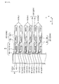
- FIG. 18 is a partially omitted cross-sectional view of the power conversion device according to the seventh embodiment.
- FIG. 19 is a circuit diagram of a power conversion device according to the eighth embodiment.
- FIG. 20 is a partially omitted cross-sectional view of the power conversion device according to the eighth embodiment.
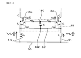
- FIG. 21 is a part of a circuit diagram of the power conversion device according to the first comparative embodiment.
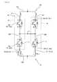
- FIG. 22 is a part of a circuit diagram of the power conversion device according to the second comparative example.
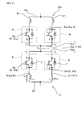
- FIG. 23 is a part of a circuit diagram of the power conversion device according to the third comparative example.
- the power conversion device can be an on-vehicle power conversion device to be mounted on a vehicle such as an electric vehicle or a hybrid vehicle.
- the power conversion device 1 of this embodiment includes an upper arm semiconductor element 2 u, a lower arm semiconductor element 2 d, a capacitor 3, a positive bus bar 4, and a negative bus bar 5.
- the upper arm semiconductor element 2u and the lower arm semiconductor element 2d are connected in series with each other.
- a plurality of upper arm semiconductor elements 2u and lower arm semiconductor elements 2d are provided.
- Freewheel diodes 7 are connected in reverse parallel to the upper arm semiconductor element 2u and the lower arm semiconductor element 2d, respectively.
- the capacitor 3 smoothes the DC voltage of the DC power supply 8.
- the positive bus bar 4 includes a positive main body portion 40 and a plurality of positive branch portions 41.
- the positive-side main body 40 is electrically connected to the capacitor 3.
- the positive branch 41 extends from the positive main body 40 and is electrically connected to the upper arm semiconductor element 2u.
- the negative bus bar 5 includes a negative main body portion 50 and a plurality of negative side branch portions 51.
- the negative main body 50 is electrically connected to the capacitor 3.
- the negative side branch portion 51 extends from the negative side main body portion 50 and is electrically connected to the lower arm semiconductor element 2d.
- the positive side branch portions 41 and the negative side branch portions 51 are alternately arranged. Further, as shown in FIGS. 2 and 7, a semiconductor element comprising a plurality of upper arm semiconductor elements 2u that are simultaneously turned on / off and a plurality of lower arm semiconductor elements 2d that are connected in series to the upper arm semiconductor elements 2u and are simultaneously turned on / off. A plurality of groups 20 are formed.
- the negative side branch portion 51 includes two positive side branch portions 41 connected to the upper arm semiconductor element 2u belonging to the same semiconductor element group 20 as the lower arm semiconductor element 2d to which the negative side branch portion 51 is connected. There are an intervening negative side branch portion 51i interposed therebetween and an end negative side branch portion 51e disposed at a position not interposed between the two positive side branch portions.
- the self-inductance of the end negative side branch 51e is made smaller than the self-inductance of the intervening negative side branch 51i.
- the power conversion device 1 of this embodiment is a vehicle-mounted power conversion device to be mounted on a vehicle such as an electric vehicle or a hybrid vehicle.
- the power converter 1 is connected to a DC power source 8 and a three-phase AC motor 81.
- the power conversion device 1 is configured to convert DC power supplied from the DC power supply 8 into AC power by performing on / off operations of the individual semiconductor elements 2.
- the three-phase alternating current motor 81 is driven using the obtained alternating current power, and the said vehicle is drive
- the upper arm semiconductor element 2u and the lower arm semiconductor element 2d are sealed in the main body 60 (see FIG. 3) of the semiconductor module 6. Further, as described above, in this embodiment, the plurality of semiconductor elements 2 are simultaneously turned on / off. Thereby, even if the electric current which flows into each semiconductor element 2 is low, the output current of the whole power converter device 1 is made high.
- the upper arm semiconductor element 2u is electrically connected to the positive side branch 41 (see FIG. 2) of the positive bus bar 4. Further, the lower arm semiconductor element 2 d is electrically connected to the negative side branch portion 51 of the negative bus bar 5.
- the semiconductor element group 20 includes a plurality of upper arm semiconductor elements 2u that are simultaneously turned on and off, and a plurality of lower arm semiconductor elements 2d that are connected in series to the upper arm semiconductor elements 2u and are simultaneously turned on and off. Is formed.
- the semiconductor element group 20 includes a U-phase semiconductor element group 20U, a V-phase semiconductor element group 20V, and a W-phase semiconductor element group 20W.
- FIG. 10 shows the time change of the current i flowing through the positive side branch part 41 and the negative side branch part 51.
- the current i flowing through the positive side branch portion 41 gradually increases. Further, the current i (that is, the return current) flowing through the negative side branch portion 51 is gradually reduced. At time t2, the current i flowing through the negative side branch portion 51 becomes zero. Thereafter, until time t 3, a recovery current flows through the freewheel diode 7, and this recovery current flows through the negative side branch 51.
- the time change rate di / dt of the current i flowing through the positive side branch portion 41 and the time change rate di / dt of the current i flowing through the negative side branch portion 51 are opposite to each other. Accordingly, the intervening negative side branch 51i (see FIG. 2) sandwiched between the two positive side branches 41 is more positive than the end negative side branch 51e where only one positive side branch 41 is adjacent. Since the magnetic coupling with the portion 41 is facilitated, the mutual inductance is reduced.
- the negative bus bar includes a negative side main body portion 50 and a plurality of negative side branch portions 51 extending from the negative side main body portion 50.
- a comb tooth portion 501 is formed on the negative main body portion 50.
- a negative side branch portion 51 extends from the comb tooth portion 501.
- the end negative side branch portion 51e is formed thicker than the intervening negative side branch portion 51i.
- the end negative side branch part 51e can be formed by, for example, welding a sheet metal thicker than the intervening negative side branch part 51i to the comb tooth part 501.
- the intervening negative branch 51 i is formed of the same plate-like member as the negative main body 50. That is, the negative main body 50 and the intervening negative branch 51i are formed by bending a single plate-like member.
- the positive bus bar 4 has the same structure as the negative bus bar 5.
- the positive bus bar 4 includes a plate-like positive main body portion 40 and a plurality of positive branch portions 41 extending from the positive main body portion 40. In this embodiment, all the positive side branch portions 41 have the same thickness.
- the positive main body 40 and the negative main body 50 are overlapped.
- the extending direction (hereinafter also referred to as Y direction) in which the negative side branch portion 51 extends from the negative side main body portion 50 coincides with the direction in which the positive side branch portion 41 extends from the positive side main body portion 40.
- the positive side branch part 41 and the negative side branch part 51 are arranged in an arrangement direction (hereinafter also referred to as X direction) orthogonal to the Y direction. As shown in FIG. 3, when viewed from the X direction, the positive side branch portion 41 and the negative side branch portion 51 overlap each other.
- the positive bus bar 4 and the negative bus bar 5 are connected to the capacitor 3.
- the capacitor 3 includes a capacitor element 30 and a sealing member 31 that seals the capacitor element 30.
- the semiconductor module 6 includes a main body 60 that seals the semiconductor element 2, a power terminal 61 that protrudes from the main body 60, and a control terminal 62.
- the power terminal 61 includes a positive terminal 61p connected to the positive bus bar 4, a negative terminal 61n connected to the negative bus bar 5, and an AC terminal 61a connected to the three-phase AC motor 81 (see FIG. 7).
- the control terminal 62 is connected to the control circuit board 18.
- the control circuit board 18 controls the on / off operation of the semiconductor element 2.
- a stacked body 10 is configured by alternately stacking a plurality of semiconductor modules 6 and cooling pipes 11 for cooling the semiconductor modules 6.
- Two cooling pipes 11 adjacent to each other are connected by two connecting pipes 15.
- the connecting pipe 15 is provided at both ends of the cooling pipe 11 in the Y direction.
- coolant 12 is introduce
- an introduction pipe 13 and a lead-out pipe 14 for leading out the refrigerant 12 are attached.
- the refrigerant 12 flows through all the cooling pipes 11 through the connecting pipe 15 and is led out from the outlet pipe 14.
- the semiconductor module 6 is configured to be cooled.
- a pressure member 16 (for example, a leaf spring) is disposed between the first wall portion 171 of the case 17 and the laminated body 10.
- the laminate 10 is pressed against the second wall portion 172 of the case 17 by the pressure member 16. Thereby, the contact pressure between the cooling pipe 11 and the semiconductor module 6 is secured, and the laminated body 10 is fixed in the case 17.
- FIG. 21 shows a part of a circuit of a conventional power converter.
- the end negative side branch 51e has a larger mutual inductance than the intervening negative side branch 51i.
- the end negative side branch 51e has a larger mutual inductance than the intervening negative side branch 51i.
- the negative side branches 51e and 51i have almost the same self-inductance, the end negative side branch 51e The effective inductance was large.
- the gate terminals of the two lower arm semiconductor elements 2d e and 2d i are connected to each other on the control circuit board 18.
- wirings 181 are formed to connect the emitter terminals E e and E i of the two lower arm semiconductor elements 2d e and 2d i .
- a power supply circuit 180 is provided between the wiring 181 and the gate terminal.
- the self-inductance of the end negative side branch portion 51e is reduced as in the present embodiment, the difference between the effective inductances L of the two negative side branch portions 51e and 51i can be reduced. Therefore, the reference potential of the lower arm semiconductor element 2d e connected to the end negative branch 51e, and a reference potential of the lower arm semiconductor element 2d i connected to the intervening negative branch 51i may be suppressed greatly different from each other.
- the AC bus bar 19 includes an upper arm portion 191, a lower arm portion 192, and one connecting portion 190 that connects these.
- the upper arm portion 191 connects a plurality of upper arm semiconductor elements 2u.
- the lower arm portion 192 connects a plurality of lower arm semiconductor elements 2d.
- two of the lower arm semiconductor element 2d e, the collector of 2d i is one of two upper arms semiconductor device 2u e via the connecting portion 190 of, for connecting to 2u i, the two upper arms semiconductor element 2u e, the emitter potential of 2u i (i.e., the reference potential) becomes an intermediate value V m between V e and V i, two reference potential is substantially equal.
- the effective inductance L of the negative side branch portions 51e and 51i ( If the difference between L e and L i ) is reduced, the difference between the induced electromotive forces V e and V i generated in the negative side branches 51e and 51i can be reduced. Therefore, it is possible to two upper arms semiconductor device 2u e, the reference potential V e of 2u i, the difference between V i smaller.
- the positive side branch portions 41 and the negative side branch portions 51 are alternately arranged, and a semiconductor element group 20 is configured by a plurality of semiconductor elements 2 that are connected to these branch portions and simultaneously turned on and off. is there.
- the end negative side branch 51e has a smaller self-inductance than the intervening negative side branch 51i. Therefore, the difference in the reference potentials of the plurality of lower arm semiconductor elements 2d that are simultaneously turned on / off can be reduced. That is, since the end negative side branch portion 51e is not interposed between the two positive side branch portions 41, the intervening negative side branch portion interposed between the two positive side branch portions 41 as described above.
- Mutual inductance tends to be larger than 51i.
- the end negative side branch portion 51e whose mutual inductance tends to increase, has a smaller self-inductance than the intervening negative side branch portion 51i. Therefore, the difference in effective inductance L (that is, a value obtained by adding mutual inductance and self-inductance) between the intervening negative branch 51i and the end negative branch 51e can be reduced. Therefore, as shown in FIG. 11, the induced electromotive force generated due to the effective inductance L when a current flows is unlikely to greatly differ between the intervening negative branch 51i and the end negative branch 51e.
- the laminated body 10 is configured by laminating the semiconductor module 6 and the cooling pipe 11.
- the positive side branch part 41 connected to the positive terminal 61p of the semiconductor module 6 and the negative side branch part 51 connected to the negative terminal 61n are alternately arranged.
- the end negative side branch 51e having relatively large mutual inductance is easily formed without being sandwiched. Therefore, as in the present embodiment, the effect of reducing the self-inductance of the end negative side branch 51e and reducing the effective inductance L parasitic on the two negative side branches 51e and 51i is great.
- the upper arm semiconductor element 2 u and the lower arm semiconductor element 2 d are built in one semiconductor module 6.
- two negative side branch 51e, the difference in effective inductance L parasitic respectively 51i is large, two upper arm semiconductor devices 2u e, the difference between the reference potential of 2u i increases
- the difference between the effective inductances L parasitic on the two negative side branches 51e and 51i can be reduced, the two upper arm semiconductor elements 2u as shown in FIG. e, it is possible to reduce the difference between the reference potential of 2u i.
- the thickness of the end negative side branch 51e in the X direction is larger than the thickness of the intervening negative side branch 51i in the X direction.
- the self-inductance of the end negative side branch 51e is reduced. Therefore, the self-inductance of the end negative side branch 51e can be reliably reduced, and the difference in effective inductance between the two types of negative side branches 51i and 51e can be reliably reduced.
- the IGBT is used as the semiconductor element 2.
- the present invention is not limited to this, and for example, a MOSFET or a bipolar transistor can be used.
- a MOSFET is used as the semiconductor element 2
- the potential of the source electrode becomes the reference potential.
- a bipolar transistor the potential of the emitter electrode becomes the reference potential.
- SiC or GaN can be used as the semiconductor material.
- one semiconductor element group 20 may be configured by providing three or more upper arm semiconductor elements 2u and lower arm semiconductor elements 2d that are simultaneously turned on and off.
- (Embodiment 2) In this embodiment, the shape of the negative bus bar 5 is changed. As shown in FIG. 12, in this embodiment, the length of the end negative side branch 51e in the Y direction is shorter than the length of the intervening negative side branch 51i in the Y direction. Thereby, the length of the current path of the end negative side branch 51e is shortened, and the self inductance of the end negative side branch 51e is made smaller than the self inductance of the intervening negative side branch 51i.
- the negative bus bar 5 can be easily manufactured because the end negative side branch 51e does not need to be formed thickly as in the first embodiment.
- the same configuration and operational effects as those of the first embodiment are provided.
- the negative bus bar 5 can be easily manufactured because the end negative side branch 51e does not need to be formed thickly as in the first embodiment.
- the same configuration and operational effects as those of the first embodiment are provided.
- the end negative side branch 51e is made of a conductive material different from the intervening negative side branch 51i. More specifically, in this embodiment, the end negative side branch portion 51e is made of a material having a lower electrical resistivity than the intervening negative side branch portion 51i. Thereby, the self-inductance of the end negative side branch 51e is made smaller than the self-inductance of the intervening negative side branch 51i.
- the same configuration and operational effects as those of the first embodiment are provided.
- the shape of the negative bus bar 5 is changed.
- the end negative side branch 51e is made longer than the intervening negative side branch 51i in the orthogonal direction (hereinafter also referred to as Z direction) orthogonal to both the X direction and the Y direction. is there.
- the self-inductance of the end negative side branch part 51e is made smaller than the self-inductance of the intervening negative side branch part 51i.
- the shape of the main bus bar 4 is changed.
- the positive side branch 41 of the positive bus bar 4 has two negative arms connected to the lower arm semiconductor element 2d belonging to the same semiconductor element group 20 as the upper arm semiconductor element 2u connected to the positive side branch 41.
- the end positive side branch portion 41e is formed thicker than the intervening positive side branch portion 41i. Thereby, the self-inductance of the end positive side branch part 41e is made smaller than the self-inductance of the intervening positive side branch part 41i.
- the intervening positive side branch 41i is interposed between the two negative side branches 51, the mutual inductance is relatively small. Further, since the end positive side branch portion 41e is not interposed between the two negative side branch portions 51, the mutual inductance is relatively large. Therefore, by reducing the self-inductance of the end positive side branch 41e having a relatively large mutual inductance, the effective inductance (that is, the mutual inductance and the self inductance of the intervening positive side branch 41i and the end positive side branch 41e is reduced). The difference of the added value) can be reduced. Therefore, the surge applied to the semiconductor element 2 can be made uniform. Therefore, a high surge is applied only to a part of the semiconductor elements 2, so that it is possible to suppress a problem that the life of the semiconductor elements 2 is shortened. In addition, the same configuration and operational effects as those of the first embodiment are provided.
- the self-inductance of the end positive side branch portion 41e is made smaller than that of the intervening positive side branch portion 41i by forming the end positive side branch portion 41e thick, but the present invention is not limited to this. Absent. That is, the length in the Y direction of the end positive branch 41e is shorter than that of the intervening positive branch 41i, a through hole or a concave portion is formed in the intervening positive branch 41i, or the end positive branch 41e is interposed You may comprise with the material whose electrical resistivity is smaller than the side branch part 41i. Further, in the Z direction, the end positive side branch portion 41e may be longer than the intervening positive side branch portion 41i.
- This embodiment is an example in which the number of semiconductor element groups 20 is changed. As shown in FIG. 19, in this embodiment, only one semiconductor element group 20 is formed.
- the semiconductor element group 20 constitutes a booster circuit.
- a reactor 88 is connected to the semiconductor element group 20.
- the lower arm semiconductor element 2 d is turned on and off, and the voltage of the DC power supply 8 is boosted using the reactor 88. The boosted voltage is smoothed by the capacitor 3.
- the difference in effective inductance L of the plurality of negative side branches 51 is reduced. That is, in this embodiment, as shown in FIG. 20, the positive side branch portions 41 and the negative side branch portions 51 are alternately arranged.
- the negative side branch portion 51 includes an intervening negative side branch portion 51i interposed between the two positive side branch portions 41 and an end negative side branch portion 51e disposed at a position not interposed between the two positive side branch portions 41. There is.
- the thickness of the end negative side branch portion 51e is larger than the thickness of the intervening negative side branch portion 51i. Thereby, the self-inductance of the end negative side branch part 51e is reduced, and the difference in effective inductance parasitic on the two negative side branch parts 51e and 51i is reduced. As a result, the difference in the reference potential of the lower arm semiconductor element 2d that is electrically connected to the negative side branches 51e and 51i is reduced. In addition, the same configuration and operational effects as those of the first embodiment are provided.
- the present invention is not limited to the above embodiments, and can be combined with each other.
- the end negative side branch part 51e may be formed thicker than the intervening negative side branch part 51i in the X direction, and the end positive side branch part 41e may be longer than the intervening positive side branch part 41i in the Z direction.
Landscapes
- Engineering & Computer Science (AREA)
- Power Engineering (AREA)
- Inverter Devices (AREA)
- Dc-Dc Converters (AREA)
Abstract
半導体素子(2u),(2d)と、コンデンサ(3)と、正バスバー(4)と、負バスバー(5)とを備える。負バスバー(5)は、負側本体部(50)と、複数の負側枝部(51)とを備える。負側枝部(51)には、該負側枝部(51)が接続した下アーム半導体素子(2d)と同じ半導体素子群(20)に属する上アーム半導体素子(2u)に接続した2本の正側枝部(41)の間に介在した介在負側枝部(51i)と、上記2本の正側枝部(41)の間に介在しない位置に配された端部負側枝部(51e)とがある。端部負側枝部(51e)の自己インダクタンスは、介在負側枝部(51i)の自己インダクタンスよりも小さくされている。
Description
本出願は、2015年12月25日に出願された日本出願番号2015-254463号に基づくもので、ここにその記載内容を援用する。
本開示は、複数の半導体素子と、平滑用のコンデンサと、これらを電気接続する正バスバー及び負バスバーを備える電力変換装置に関する。
インバータやDC-DCコンバータ等の電力変換装置として、IGBT等の半導体素子と、平滑用のコンデンサと、これらを電気接続する正バスバー及び負バスバーを備えるものが知られている(下記特許文献1参照)。
上記正バスバーは、コンデンサに接続した正側本体部と、該正側本体部から延出し上記半導体素子に接続した複数の正側枝部とを備える。また、負バスバーは、コンデンサに接続した負側本体部と、該負側本体部から延出し半導体素子に接続した複数の負側枝部とを備える。正側枝部と負側枝部とは、交互に配されている。これにより、正側枝部と負側枝部とを互いに接近させ、これらに寄生するインダクタンスを低減させている。
一方、近年、互いに並列接続された複数の半導体素子を同時にオンオフ動作させ、これにより、個々の半導体素子を流れる電流は低くても、全体の出力電流を高くすることができる電力変換装置の開発が進められている。
しかしながら、発明者の詳細な検討の結果、正側枝部と負側枝部とを交互に配置し、かつ複数の半導体素子を同時にオンオフすると、以下の課題が生じることが見出された。
すなわち、負側枝部には、それぞれ相互インダクタンスと自己インダクタンスとが寄生している。正側枝部と負側枝部とを交互に配置し、これらの枝部に接続した複数の半導体素子を同時にオンオフすると、後述するように、相互インダクタンスと自己インダクタンスとの和である実効インダクタンスが、負側枝部ごとに大きく異なりやすい。そのため、電流が流れたときに実効インダクタンスが原因となって発生する誘導起電力が、負側枝部ごとに大きく異なりやすくなる。したがって、これらの負側枝部に電気接続し同時にオンオフ動作する複数の半導体素子の、エミッタ等の基準電極の電位(すなわち、基準電位)が、互いに大きく異なりやすくなる。そのため後述するように、一部の半導体素子の制御端子に高い電圧が加わる可能性が考えられる。
すなわち、負側枝部には、それぞれ相互インダクタンスと自己インダクタンスとが寄生している。正側枝部と負側枝部とを交互に配置し、これらの枝部に接続した複数の半導体素子を同時にオンオフすると、後述するように、相互インダクタンスと自己インダクタンスとの和である実効インダクタンスが、負側枝部ごとに大きく異なりやすい。そのため、電流が流れたときに実効インダクタンスが原因となって発生する誘導起電力が、負側枝部ごとに大きく異なりやすくなる。したがって、これらの負側枝部に電気接続し同時にオンオフ動作する複数の半導体素子の、エミッタ等の基準電極の電位(すなわち、基準電位)が、互いに大きく異なりやすくなる。そのため後述するように、一部の半導体素子の制御端子に高い電圧が加わる可能性が考えられる。
本開示は、同時にオンオフ動作する複数の半導体素子の、基準電位の差を小さくすることができる電力変換装置を提供することを目的とする。
本開示の第1の態様は、互いに直列接続され、それぞれ複数個設けられた、上アーム半導体素子と下アーム半導体素子との半導体素子と、
個々の該半導体素子に逆並列接続したフリーホイールダイオードと、
直流電圧を平滑化するコンデンサと、
該コンデンサに電気接続した正側本体部と、該正側本体部から延出し上記上アーム半導体素子に電気接続した複数の正側枝部とを有する正バスバーと、
上記コンデンサに電気接続した負側本体部と、該負側本体部から延出し上記下アーム半導体素子に電気接続した複数の負側枝部とを有する負バスバーとを備え、
上記正側枝部と上記負側枝部とは交互に配されており、
同時にオンオフ動作する複数の上記上アーム半導体素子と、該上アーム半導体素子に直列接続し同時にオンオフ動作する複数の上記下アーム半導体素子とからなる半導体素子群が形成され、
上記負側枝部には、該負側枝部が接続した上記下アーム半導体素子と同じ上記半導体素子群に属する上記上アーム半導体素子に接続した2本の上記正側枝部の間に介在した介在負側枝部と、上記2本の正側枝部の間に介在しない位置に配された端部負側枝部とがあり、該端部負側枝部の自己インダクタンスを、上記介在負側枝部の自己インダクタンスよりも小さくしてある、電力変換装置にある。
個々の該半導体素子に逆並列接続したフリーホイールダイオードと、
直流電圧を平滑化するコンデンサと、
該コンデンサに電気接続した正側本体部と、該正側本体部から延出し上記上アーム半導体素子に電気接続した複数の正側枝部とを有する正バスバーと、
上記コンデンサに電気接続した負側本体部と、該負側本体部から延出し上記下アーム半導体素子に電気接続した複数の負側枝部とを有する負バスバーとを備え、
上記正側枝部と上記負側枝部とは交互に配されており、
同時にオンオフ動作する複数の上記上アーム半導体素子と、該上アーム半導体素子に直列接続し同時にオンオフ動作する複数の上記下アーム半導体素子とからなる半導体素子群が形成され、
上記負側枝部には、該負側枝部が接続した上記下アーム半導体素子と同じ上記半導体素子群に属する上記上アーム半導体素子に接続した2本の上記正側枝部の間に介在した介在負側枝部と、上記2本の正側枝部の間に介在しない位置に配された端部負側枝部とがあり、該端部負側枝部の自己インダクタンスを、上記介在負側枝部の自己インダクタンスよりも小さくしてある、電力変換装置にある。
上記電力変換装置においては、正側枝部と負側枝部とを交互に配置し、これらの枝部に接続し同時にオンオフする複数の半導体素子によって上記半導体素子群を構成してある。そして、複数の負側枝部のうち上記端部負側枝部を、上記介在負側枝部よりも、自己インダクタンスが小さくなるようにしてある。
そのため、同時にオンオフする複数の半導体素子の、基準電位の差を小さくすることができる。すなわち、上記端部負側枝部は、上記2本の正側枝部の間に介在していないため、後述するように、上記2本の正側枝部の間に介在する上記介在負側枝部よりも相互インダクタンスが大きくなりやすい。本態様では、相互インダクタンスが大きくなりやすい端部負側枝部は、介在負側枝部よりも自己インダクタンスを小さくしてある。そのため、介在負側枝部と端部負側枝部との、実効インダクタンス(すなわち、相互インダクタンスと自己インダクタンスとを加えた値)の差を小さくすることができる。そのため、電流が流れたときに実効インダクタンスが原因となって生じる誘導起電力が、介在負側枝部と端部負側枝部とで大きく異なりにくくなる。したがって、介在負側枝部に電気接続した半導体素子の基準電位と、端部負側枝部に電気接続した半導体素子の基準電位との差を、小さくすることが可能になる。つまり、これらの負側枝部に電気接続し同時にオンオフする複数の半導体素子の、基準電位の差を小さくすることができる。そのため、一部の半導体素子にのみ制御端子に高い電圧が加わる不具合を抑制することが可能になる。
そのため、同時にオンオフする複数の半導体素子の、基準電位の差を小さくすることができる。すなわち、上記端部負側枝部は、上記2本の正側枝部の間に介在していないため、後述するように、上記2本の正側枝部の間に介在する上記介在負側枝部よりも相互インダクタンスが大きくなりやすい。本態様では、相互インダクタンスが大きくなりやすい端部負側枝部は、介在負側枝部よりも自己インダクタンスを小さくしてある。そのため、介在負側枝部と端部負側枝部との、実効インダクタンス(すなわち、相互インダクタンスと自己インダクタンスとを加えた値)の差を小さくすることができる。そのため、電流が流れたときに実効インダクタンスが原因となって生じる誘導起電力が、介在負側枝部と端部負側枝部とで大きく異なりにくくなる。したがって、介在負側枝部に電気接続した半導体素子の基準電位と、端部負側枝部に電気接続した半導体素子の基準電位との差を、小さくすることが可能になる。つまり、これらの負側枝部に電気接続し同時にオンオフする複数の半導体素子の、基準電位の差を小さくすることができる。そのため、一部の半導体素子にのみ制御端子に高い電圧が加わる不具合を抑制することが可能になる。
以上のごとく、上記態様によれば、同時にオンオフ動作する複数の半導体素子の、基準電位の差を小さくすることができる電力変換装置を提供することができる。
なお、特許請求の範囲及び課題を解決する手段に記載した括弧内の符号は、後述する実施形態に記載の具体的手段との対応関係を示すものであり、本発明の技術的範囲を限定するものではない。
なお、特許請求の範囲及び課題を解決する手段に記載した括弧内の符号は、後述する実施形態に記載の具体的手段との対応関係を示すものであり、本発明の技術的範囲を限定するものではない。
本開示についての上記目的およびその他の目的、特徴や利点は、添付の図面を参照しながら下記の詳細な記述により、より明確になる。その図面は、
図1は、実施形態1における、電力変換装置の断面図であって、図3のI-I断面図である。
図2は、実施形態1における、電力変換装置の一部省略断面図である。
図3は、図1のIII-III断面図である。
図4は、実施形態1における、正バスバーを取り除いた電力変換装置の断面図である。
図5は、実施形態1における、正バスバー及び負バスバーを取り除いた電力変換装置の断面図である。
図6は、実施形態1における、負バスバーの要部拡大斜視図である。
図7は、実施形態1における、電力変換装置の回路図である。
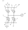
図8は、実施形態1における、上アーム半導体素子がオフしたときの、電力変換装置の回路図の一部である。
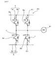
図9は、実施形態1における、上アーム半導体素子がオンしたときの、電力変換装置の回路図の一部である。
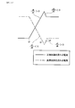
図10は、実施形態1における、上アーム半導体素子をオフからオンに切り替えたときの、正側枝部と負側枝部とに流れる電流の変化を表したグラフである。
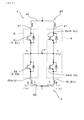
図11は、実施形態1における、1個の半導体モジュールに上アーム半導体素子と下アーム半導体素子とが内蔵されている場合でも、上アーム半導体素子の基準電位の差を小さくすることができる理由を説明するための図である。
図12は、実施形態2における、電力変換装置の一部省略断面図である。
図13は、実施形態3における、電力変換装置の断面図である。
図14は、実施形態3における、電力変換装置の要部拡大断面図である。
図15は、実施形態4における、電力変換装置の要部拡大断面図である。
図16は、実施形態5における、電力変換装置の要部拡大断面図である。
図17は、実施形態6における、負バスバーの要部拡大斜視図である。
図18は、実施形態7における、電力変換装置の一部省略断面図である。
図19は、実施形態8における、電力変換装置の回路図である。
図20は、実施形態8における、電力変換装置の一部省略断面図である。
図21は、比較形態1における、電力変換装置の回路図の一部である。
図22は、比較形態2における、電力変換装置の回路図の一部である。
図23は、比較形態3における、電力変換装置の回路図の一部である。
上記電力変換装置は、電気自動車やハイブリッド車等の車両に搭載するための、車載用電力変換装置とすることができる。
(実施形態1)
上記電力変換装置に係る実施形態について、図1~図11を参照して説明する。図1、図2に示すごとく、本形態の電力変換装置1は、上アーム半導体素子2uと、下アーム半導体素子2dと、コンデンサ3と、正バスバー4と、負バスバー5とを備える。
上記電力変換装置に係る実施形態について、図1~図11を参照して説明する。図1、図2に示すごとく、本形態の電力変換装置1は、上アーム半導体素子2uと、下アーム半導体素子2dと、コンデンサ3と、正バスバー4と、負バスバー5とを備える。
図7に示すごとく、上アーム半導体素子2uと下アーム半導体素子2dとは、互いに直列接続されている。上アーム半導体素子2uと下アーム半導体素子2dとは、それぞれ複数個、設けられている。上アーム半導体素子2uと下アーム半導体素子2dとには、それぞれフリーホイールダイオード7が逆並列接続している。
コンデンサ3は、直流電源8の直流電圧を平滑化している。
コンデンサ3は、直流電源8の直流電圧を平滑化している。
図2、図3に示すごとく、正バスバー4は、正側本体部40と、複数の正側枝部41とを備える。正側本体部40は、コンデンサ3に電気接続している。また、正側枝部41は、正側本体部40から延出し、上アーム半導体素子2uに電気接続している。
負バスバー5は、負側本体部50と、複数の負側枝部51とを備える。負側本体部50は、コンデンサ3に電気接続している。また、負側枝部51は、負側本体部50から延出し、下アーム半導体素子2dに電気接続している。
負バスバー5は、負側本体部50と、複数の負側枝部51とを備える。負側本体部50は、コンデンサ3に電気接続している。また、負側枝部51は、負側本体部50から延出し、下アーム半導体素子2dに電気接続している。
図2に示すごとく、正側枝部41と負側枝部51とは、交互に配されている。また、図2、図7に示すごとく、同時にオンオフ動作する複数の上アーム半導体素子2uと、該上アーム半導体素子2uに直列接続し同時にオンオフ動作する複数の下アーム半導体素子2dとからなる半導体素子群20が、複数個形成されている。
図2に示すごとく、負側枝部51には、該負側枝部51が接続した下アーム半導体素子2dと同じ半導体素子群20に属する上アーム半導体素子2uに接続した2本の正側枝部41の間に介在した介在負側枝部51iと、上記2本の正側枝部の間に介在しない位置に配された端部負側枝部51eとがある。
端部負側枝部51eの自己インダクタンスは、介在負側枝部51iの自己インダクタンスよりも小さくされている。
端部負側枝部51eの自己インダクタンスは、介在負側枝部51iの自己インダクタンスよりも小さくされている。
本形態の電力変換装置1は、電気自動車やハイブリッド車等の車両に搭載するための、車載用電力変換装置である。
図7に示すごとく、電力変換装置1は、直流電源8と三相交流モータ81とに接続している。電力変換装置1は、個々の半導体素子2をオンオフ動作することにより、直流電源8から供給された直流電力を交流電力に変換するよう構成されている。そして、得られた交流電力を用いて三相交流モータ81を駆動し、上記車両を走行させている。
上アーム半導体素子2uと下アーム半導体素子2dとは、半導体モジュール6の本体部60(図3参照)内に封止されている。また、上述したように、本形態では、複数の半導体素子2を同時にオンオフ動作させている。これにより、個々の半導体素子2に流れる電流が低くても、電力変換装置1全体の出力電流が高くなるようにしている。
上アーム半導体素子2uは、正バスバー4の正側枝部41(図2参照)に電気接続している。また、下アーム半導体素子2dは、負バスバー5の負側枝部51に電気接続している。
上述したように、本形態では、同時にオンオフ動作する複数の上アーム半導体素子2uと、該上アーム半導体素子2uに直列接続され同時にオンオフ動作する複数の下アーム半導体素子2dとにより、半導体素子群20を形成してある。半導体素子群20には、U相用半導体素子群20Uと、V相用半導体素子群20Vと、W相用半導体素子群20Wとがある。
次に、介在負側枝部51iの方が端部負側枝部51eよりも相互インダクタンスが小さくなる理由について説明する。図8に示すごとく、半導体素子群20を構成する全ての半導体素子2(2u,2d)をオフにした状態から、図9に示すごとく、上アーム半導体素子2uをオンにした場合を考える。図8に示すごとく、上アーム半導体素子2uをオフしている間、誘導性負荷である三相交流モータ81の働きによって、下アーム半導体素子2dに逆並列接続したフリーホイールダイオード7に還流電流iが流れている。この還流電流iは、負側枝部51を流れる。この後、図9に示すごとく、上アーム半導体素子2uをオンすると、上アーム半導体素子2uに流れる電流iが徐々に増加する。すなわち、正側枝部41を流れる電流iが徐々に増加する。また、下アーム半導体素子2dのフリーホイールダイオード7に逆バイアスが加わるため、還流電流iは徐々に低減する。
図10に、正側枝部41と負側枝部51とを流れる電流iの時間変化を示す。同図に示すごとく、時刻t1において上アーム半導体素子2uをオンすると、正側枝部41に流れる電流iが徐々に増加する。また、負側枝部51に流れる電流i(すなわち、還流電流)は徐々に低減する。時刻t2において、負側枝部51に流れる電流iは0になる。その後、時刻t3まで、フリーホイールダイオード7にリカバリー電流が流れ、このリカバリー電流が負側枝部51を流れる。
図10に示すごとく、正側枝部41を流れる電流iの時間変化率di/dtと、負側枝部51を流れる電流iの時間変化率di/dtとは、正負が逆になっている。したがって、2本の正側枝部41に挟まれた介在負側枝部51i(図2参照)の方が、一本の正側枝部41が隣り合うだけの端部負側枝部51eよりも、正側枝部41と磁気結合しやすくなるため、相互インダクタンスが小さくなる。
次に、負バスバー5の構造について説明する。図6に示すごとく、負バスバーは、負側本体部50と、該負側本体部50から延出する複数の負側枝部51とを備える。負側本体部50には櫛歯部501が形成されている。この櫛歯部501から、負側枝部51が延出している。また、端部負側枝部51eは、介在負側枝部51iよりも厚く形成されている。端部負側枝部51eは、例えば、介在負側枝部51iよりも厚い板金を、櫛歯部501に溶接することにより形成することができる。また、介在負側枝部51iは、負側本体部50と同一の板状部材により形成されている。すなわち、一枚の板状部材を折り曲げることにより、負側本体部50と、介在負側枝部51iとを形成してある。
図2、図3に示すごとく、正バスバー4も負バスバー5と同様の構造になっている。正バスバー4は、板状の正側本体部40と、該正側本体部40から延出する複数の正側枝部41とを備える。本形態では、全ての正側枝部41の厚さを同一にしてある。
図2、図3に示すごとく、正側本体部40と負側本体部50とは、重ね合されている。また、負側本体部50から負側枝部51が延出する延出方向(以下、Y方向とも記す)と、正側本体部40から正側枝部41が延出する方向とは、一致している。正側枝部41と負側枝部51とは、Y方向に直交する配列方向(以下、X方向とも記す)に配列している。図3に示すごとく、X方向から見たときに、正側枝部41と負側枝部51とは互いに重なっている。
また、正バスバー4と負バスバー5とは、コンデンサ3に接続している。コンデンサ3は、コンデンサ素子30と、該コンデンサ素子30を封止する封止部材31とを備える。
また、図3に示すごとく、上記半導体モジュール6は、半導体素子2を封止した本体部60と、該本体部60から突出したパワー端子61と、制御端子62とを備える。パワー端子61には、正バスバー4に接続した正端子61pと、負バスバー5に接続した負端子61nと、三相交流モータ81(図7参照)に接続される交流端子61aとがある。また、制御端子62は、制御回路基板18に接続している。この制御回路基板18によって、半導体素子2のオンオフ動作を制御している。
図5に示すごとく、本形態では、半導体モジュール6と、該半導体モジュール6を冷却する冷却管11とを交互に複数個、積層して、積層体10を構成している。互いに隣り合う2本の冷却管11は、2個の連結管15によって連結されている。連結管15は、Y方向における、冷却管11の両端に設けられている。
また、複数の冷却管11のうち、正側枝部41と負側枝部との配列方向(すなわち、X方向:図2参照)における一端に位置する端部冷却管11aには、冷媒12を導入するための導入管13と、冷媒12を導出するための導出管14とが取り付けられている。導入管13から冷媒12を導入すると、冷媒12は、連結管15を通って全ての冷却管11内を流れ、導出管14から導出する。これにより、半導体モジュール6を冷却するよう構成されている。
また、ケース17の第1壁部171と積層体10との間には、加圧部材16(例えば、板ばね)が配されている。この加圧部材16によって積層体10をケース17の第2壁部172に押し当てている。これにより、冷却管11と半導体モジュール6との接触圧を確保すると共に、積層体10をケース17内に固定している。
次に、端部負側枝部51eと介在負側枝部51iとの実効インダクタンスが互いに大きく異なると、これらの負側枝部51e,51iに接続した負側半導体素子2dの基準電位が大きく異なりやすくなる理由について説明する。図21に、従来の電力変換装置の回路の一部を示す。同図に示すごとく、従来は、端部負側枝部51eの実効インダクタンスLeの方が介在負側枝部51iの実効インダクタンスLiよりも大きかった。つまり、端部負側枝部51eは介在負側枝部51iよりも相互インダクタンスが大きいが、これらの負側枝部51e,51iの自己インダクタンスが殆ど同じであるため、端部負側枝部51eの方が、実効インダクタンスが大きくなっていた。また、2つの下アーム半導体素子2de,2diのゲート端子同士は、制御回路基板18において接続されている。制御回路基板18には、2つの下アーム半導体素子2de,2diのエミッタ端子Ee,Eiを繋ぐ配線181を形成してある。配線181とゲート端子との間に、電源回路180が設けられている。
ここで、2つの下アーム半導体素子2de,2diを同時にオンする場合を考える。上述したように、端部負側枝部51eの実効インダクタンスLeは大きいため、電流iが流れ始めたときに、この実効インダクタンスLeによって、比較的大きな誘導起電力Ve(=Ledi/dt)が発生する。これに対して、介在負側枝部51iの実効インダクタンスLiは小さいため、発生する誘導起電力Vi(=Lidi/dt)は小さい。そのため、端部負側枝部51eに接続したエミッタ端子Eeの電位は、介在負側枝部51iに接続したエミッタ端子Eiの電位よりも高くなる。
このように、端部負側枝部51eに接続した下アーム半導体素子2deと、介在負側枝部51iに接続した下アーム半導体素子2diとの、エミッタ端子(すなわち、基準電極)の電位(すなわち、基準電位)が互いに大きく異なると、一部の半導体素子2diのエミッタ端子-ゲート端子間に高い電圧が加わる可能性が考えられる。
これに対して、本形態のように、端部負側枝部51eの自己インダクタンスを低減すれば、2つの負側枝部51e,51iの実効インダクタンスLの差を低減することができる。そのため、端部負側枝部51eに接続した下アーム半導体素子2deの基準電位と、介在負側枝部51iに接続した下アーム半導体素子2diの基準電位とが、互いに大きく異なることを抑制できる。
一方、1個の半導体モジュール6に1個の半導体素子2のみが内蔵されている場合(図23参照)、負側枝部51e,51iの実効インダクタンスLの差が大きくなっても、2つの上アーム半導体素子2ue,2uiの基準電位の差は大きくなりにくい。しかしながら、本形態のように、1個の半導体モジュール6に上アーム半導体素子2uと下アーム半導体素子2dとを内蔵してある場合、負側枝部51e,51iの実効インダクタンスLの差が大きくなると、2つの上アーム半導体素子2ue,2uiの基準電位の差が大きくなりやすい。その理由について説明する。図23に示すごとく、1個の半導体モジュール6に1個の半導体素子2のみを内蔵した場合は、上アーム半導体素子2uのエミッタ端子と、下アーム半導体素子2dのコレクタ端子とが、交流バスバー19によって接続される。交流バスバー19は、上アーム部191と、下アーム部192と、これらを繋ぐ1本の連結部190とを備える。上アーム部191は、複数の上アーム半導体素子2u同士を接続している。下アーム部192は、複数の下アーム半導体素子2d同士を接続している。
ここで、負側枝部51e,51iの実効インダクタンスL(Le,Li)の違いによって、ある瞬間、2つの負側枝部51e,51iに互いに異なる誘導起電力Ve,Viがそれぞれ発生したとする。このとき、フリーホイールダイオード7に順方向電圧が加わって導通するため、下アーム半導体素子2de,2diのコレクタの電位は、それぞれ、略Ve,Viとなる。しかし、2つの下アーム半導体素子2de,2diのコレクタは、1本の連結部190を介して2つの上アーム半導体素子2ue,2uiに接続しているため、これら2つの上アーム半導体素子2ue,2uiのエミッタの電位(すなわち、基準電位)は、VeとViとの中間値Vmになり、これら2つの基準電位は略等しくなる。
これに対して、図22に示すごとく、1個の半導体モジュール6に上アーム半導体素子2uと下アーム半導体素子2dとが内蔵されている場合は、2つの負側枝部51e,51iの実効インダクタンスLに大きな差があると、上アーム半導体素子2ue,2uiの基準電位の差が大きくなりやすい。すなわち、この場合、各半導体モジュール6内において、上アーム半導体素子2uと下アーム半導体素子2dとが、半導体モジュール6内の導電性部材69によって個別に接続される。つまり、2つの下アーム半導体素子2de,2diが、それぞれ別々に、上アーム半導体素子2ue,2uiに接続される。そのため、実効インダクタンスL(Le,Li)の違いによって負枝部51e,51iに互いに異なる誘導起電力Ve,Viが発生した場合、フリーホイールダイオード7が導通し、2つの上アーム半導体素子2ue,2uiのエミッタの電位が、互いに異なる値Ve,Viになる。
したがって、本形態のように、上アーム半導体素子2uと下アーム半導体素子2dとを1個の半導体モジュール6に内蔵する場合は、図11に示すごとく、負側枝部51e,51iの実効インダクタンスL(Le,Li)の差を小さくすれば、負側枝部51e,51iに発生する誘導起電力Ve,Viの差を小さくすることができる。そのため、2つの上アーム半導体素子2ue,2uiの基準電位Ve,Viの差を小さくすることができる。
次に、本形態の作用効果について説明する。本形態では、図2に示すごとく、正側枝部41と負側枝部51とを交互に配置し、これらの枝部に接続し同時にオンオフする複数の半導体素子2によって半導体素子群20を構成してある。そして、複数の負側枝部51のうち上記端部負側枝部51eを、上記介在負側枝部51iよりも、自己インダクタンスが小さくなるようにしてある。
そのため、同時にオンオフする複数の下アーム半導体素子2dの、基準電位の差を小さくすることができる。すなわち、上記端部負側枝部51eは、上記2本の正側枝部41の間に介在していないため、上述したように、上記2本の正側枝部41の間に介在する介在負側枝部51iよりも相互インダクタンスが大きくなりやすい。本形態では、相互インダクタンスが大きくなりやすい端部負側枝部51eは、介在負側枝部51iよりも自己インダクタンスを小さくしてある。そのため、介在負側枝部51iと端部負側枝部51eとの、実効インダクタンスL(すなわち、相互インダクタンスと自己インダクタンスとを加えた値)の差を小さくすることができる。そのため、図11に示すごとく、電流が流れたときに実効インダクタンスLが原因となって生じる誘導起電力が、介在負側枝部51iと端部負側枝部51eとで大きく異なりにくくなる。したがって、介在負側枝部51iに接続した下アーム半導体素子2diの基準電位と、端部負側枝部51eに接続した下アーム半導体素子2deの基準電位との差を、小さくすることが可能になる。つまり、これらの負側枝部51i,51eに接続し同時にオンオフする複数の下アーム半導体素子2di,2deの基準電位の差を、小さくすることが可能になる。そのため、一部の下アーム半導体素子2dにのみ制御端子に高い電圧が加わる問題を抑制できる。
そのため、同時にオンオフする複数の下アーム半導体素子2dの、基準電位の差を小さくすることができる。すなわち、上記端部負側枝部51eは、上記2本の正側枝部41の間に介在していないため、上述したように、上記2本の正側枝部41の間に介在する介在負側枝部51iよりも相互インダクタンスが大きくなりやすい。本形態では、相互インダクタンスが大きくなりやすい端部負側枝部51eは、介在負側枝部51iよりも自己インダクタンスを小さくしてある。そのため、介在負側枝部51iと端部負側枝部51eとの、実効インダクタンスL(すなわち、相互インダクタンスと自己インダクタンスとを加えた値)の差を小さくすることができる。そのため、図11に示すごとく、電流が流れたときに実効インダクタンスLが原因となって生じる誘導起電力が、介在負側枝部51iと端部負側枝部51eとで大きく異なりにくくなる。したがって、介在負側枝部51iに接続した下アーム半導体素子2diの基準電位と、端部負側枝部51eに接続した下アーム半導体素子2deの基準電位との差を、小さくすることが可能になる。つまり、これらの負側枝部51i,51eに接続し同時にオンオフする複数の下アーム半導体素子2di,2deの基準電位の差を、小さくすることが可能になる。そのため、一部の下アーム半導体素子2dにのみ制御端子に高い電圧が加わる問題を抑制できる。
また、本形態では、図1に示すごとく、半導体モジュール6と冷却管11とを積層して積層体10を構成してある。
この場合には、半導体モジュール6の正端子61pに接続した正側枝部41と、負端子61nに接続した負側枝部51とが、交互に配列される。そのため、同じ半導体素子群20に属する上アーム半導体素子2uに接続した2本の正側枝部41に挟まれ、相互インダクタンスが相対的に小さい介在負側枝部51iと、上記2本の正側枝部に挟まれず、相互インダクタンスが相対的に大きい端部負側枝部51eとが形成されやすい。そのため、本形態のように、端部負側枝部51eの自己インダクタンスを低減して、2つの負側枝部51e,51iに寄生する実効インダクタンスLの差を小さくした場合の効果は大きい。
この場合には、半導体モジュール6の正端子61pに接続した正側枝部41と、負端子61nに接続した負側枝部51とが、交互に配列される。そのため、同じ半導体素子群20に属する上アーム半導体素子2uに接続した2本の正側枝部41に挟まれ、相互インダクタンスが相対的に小さい介在負側枝部51iと、上記2本の正側枝部に挟まれず、相互インダクタンスが相対的に大きい端部負側枝部51eとが形成されやすい。そのため、本形態のように、端部負側枝部51eの自己インダクタンスを低減して、2つの負側枝部51e,51iに寄生する実効インダクタンスLの差を小さくした場合の効果は大きい。
また、本形態では、図2、図11に示すごとく、上アーム半導体素子2uと下アーム半導体素子2dとが、1個の半導体モジュール6に内蔵されている。
この場合には、上述したように、2つの負側枝部51e,51iにそれぞれ寄生する実効インダクタンスLの差が大きいと、2つの上アーム半導体素子2ue,2uiの基準電位の差が大きくなりやすいが(図22参照)、本形態では、2つの負側枝部51e,51iにそれぞれ寄生する実効インダクタンスLの差を小さくすることができるため、図11に示すごとく、2つの上アーム半導体素子2ue,2uiの基準電位の差を小さくすることができる。
この場合には、上述したように、2つの負側枝部51e,51iにそれぞれ寄生する実効インダクタンスLの差が大きいと、2つの上アーム半導体素子2ue,2uiの基準電位の差が大きくなりやすいが(図22参照)、本形態では、2つの負側枝部51e,51iにそれぞれ寄生する実効インダクタンスLの差を小さくすることができるため、図11に示すごとく、2つの上アーム半導体素子2ue,2uiの基準電位の差を小さくすることができる。
また、本形態では、図2に示すごとく、X方向における端部負側枝部51eの厚さを、X方向における介在負側枝部51iの厚さよりも厚くしてある。これにより、端部負側枝部51eの自己インダクタンスを低減している。
そのため、端部負側枝部51eの自己インダクタンスを確実に低減でき、2種類の負側枝部51i,51eの実効インダクタンスの差を確実に小さくすることができる。
そのため、端部負側枝部51eの自己インダクタンスを確実に低減でき、2種類の負側枝部51i,51eの実効インダクタンスの差を確実に小さくすることができる。
以上のごとく、本形態によれば、同時にオンオフ動作する複数の半導体素子の、基準電位の差を小さくすることができる電力変換装置を提供することができる。
なお、本形態では、半導体素子2としてIGBTを用いたが、本発明はこれに限るものではなく、例えばMOSFETやバイポーラトランジスタを用いることもできる。半導体素子2としてMOSFETを用いた場合、ソース電極の電位が基準電位になる。また、バイポーラトランジスタを用いる場合は、エミッタ電極の電位が、基準電位になる。また、半導体材料として、SiCやGaNを用いることもできる。
また、本形態では、同時にオンオフ動作する上アーム半導体素子2uと下アーム半導体素子2dとを、それぞれ2個ずつ設けて、一つの半導体素子群20を構成したが、本発明はこれに限るものではない。すなわち、同時にオンオフ動作する上アーム半導体素子2uと下アーム半導体素子2dとをそれぞれ3個以上設けて、一つの半導体素子群20を構成してもよい。
以下の実施形態においては、図面に用いた符号のうち、実施形態1において用いた符号と同一のものは、特に示さない限り、実施形態1と同様の構成要素等を表す。
(実施形態2)
本形態は、負バスバー5の形状を変更した例である。図12に示すごとく、本形態では、Y方向における端部負側枝部51eの長さを、Y方向における介在負側枝部51iの長さよりも短くしている。これにより、端部負側枝部51eの電流経路の長さを短くし、端部負側枝部51eの自己インダクタンスを介在負側枝部51iの自己インダクタンスよりも小さくしている。
本形態は、負バスバー5の形状を変更した例である。図12に示すごとく、本形態では、Y方向における端部負側枝部51eの長さを、Y方向における介在負側枝部51iの長さよりも短くしている。これにより、端部負側枝部51eの電流経路の長さを短くし、端部負側枝部51eの自己インダクタンスを介在負側枝部51iの自己インダクタンスよりも小さくしている。
上記構成にすると、実施形態1のように、端部負側枝部51eを厚く形成する必要がないため、負バスバー5を容易に製造することが可能になる。
その他、実施形態1と同様の構成および作用効果を備える。
その他、実施形態1と同様の構成および作用効果を備える。
(実施形態3)
本形態は、負バスバー5の形状を変更した例である。図13、図14に示すごとく、本形態では、介在負側枝部51iに貫通孔58を形成してある。これにより、介在負側枝部51iに、電流密度が局所的に高くなる部位580を形成し、介在負側枝部51iの自己インダクタンスを大きくしている。これによって、端部負側枝部51eの自己インダクンタスを、介在負側枝部51iの自己インダクタンスよりも相対的に小さくしている。
本形態は、負バスバー5の形状を変更した例である。図13、図14に示すごとく、本形態では、介在負側枝部51iに貫通孔58を形成してある。これにより、介在負側枝部51iに、電流密度が局所的に高くなる部位580を形成し、介在負側枝部51iの自己インダクタンスを大きくしている。これによって、端部負側枝部51eの自己インダクンタスを、介在負側枝部51iの自己インダクタンスよりも相対的に小さくしている。
上記構成にすると、実施形態1のように、端部負側枝部51eを厚く形成しなくてすむため、負バスバー5を容易に製造することができる。
その他、実施形態1と同様の構成および作用効果を備える。
その他、実施形態1と同様の構成および作用効果を備える。
(実施形態4)
本形態は、負バスバー5の形状を変更した例である。図15に示すごとく、本形態では、介在負側枝部51iに凹状部59を形成してある。これにより、介在負側枝部51iに、電流密度が局所的に高くなる部位590を形成し、介在負側枝部51iの自己インダクタンスを大きくしている。これによって、端部負側枝部51eの自己インダクンタスを、介在負側枝部51iの自己インダクタンスよりも相対的に小さくしている。
本形態は、負バスバー5の形状を変更した例である。図15に示すごとく、本形態では、介在負側枝部51iに凹状部59を形成してある。これにより、介在負側枝部51iに、電流密度が局所的に高くなる部位590を形成し、介在負側枝部51iの自己インダクタンスを大きくしている。これによって、端部負側枝部51eの自己インダクンタスを、介在負側枝部51iの自己インダクタンスよりも相対的に小さくしている。
上記構成にすると、実施形態1のように、端部負側枝部51eを厚く形成しなくてすむため、負バスバー5を容易に製造することができる。
その他、実施形態1と同様の構成および作用効果を備える。
その他、実施形態1と同様の構成および作用効果を備える。
(実施形態5)
本形態は、負バスバー5の構造を変更した例である。図16に示すごとく、本形態では、端部負側枝部51eを、介在負側枝部51iとは異なる導電材料によって構成してある。より詳しくは、本形態では、端部負側枝部51eを、介在負側枝部51iよりも電気抵抗率が小さい材料によって構成している。これにより、端部負側枝部51eの自己インダクタンスを、介在負側枝部51iの自己インダクタンスよりも小さくしている。
その他、実施形態1と同様の構成および作用効果を備える。
本形態は、負バスバー5の構造を変更した例である。図16に示すごとく、本形態では、端部負側枝部51eを、介在負側枝部51iとは異なる導電材料によって構成してある。より詳しくは、本形態では、端部負側枝部51eを、介在負側枝部51iよりも電気抵抗率が小さい材料によって構成している。これにより、端部負側枝部51eの自己インダクタンスを、介在負側枝部51iの自己インダクタンスよりも小さくしている。
その他、実施形態1と同様の構成および作用効果を備える。
(実施形態6)
本形態は、負バスバー5の形状を変更した例である。図17に示すごとく、本形態では、X方向とY方向との双方に直交する直交方向(以下、Z方向とも記す)において、端部負側枝部51eを介在負側枝部51iよりも長くしてある。これにより、端部負側枝部51eの自己インダクタンスを、介在負側枝部51iの自己インダクタンスよりも小さくしてある。
上記構成にすると、実施形態1のように、端部負側枝部51eを厚く形成しなくてすむため、負バスバー5を容易に製造することができる。
その他、実施形態1と同様の構成および作用効果を備える。
本形態は、負バスバー5の形状を変更した例である。図17に示すごとく、本形態では、X方向とY方向との双方に直交する直交方向(以下、Z方向とも記す)において、端部負側枝部51eを介在負側枝部51iよりも長くしてある。これにより、端部負側枝部51eの自己インダクタンスを、介在負側枝部51iの自己インダクタンスよりも小さくしてある。
上記構成にすると、実施形態1のように、端部負側枝部51eを厚く形成しなくてすむため、負バスバー5を容易に製造することができる。
その他、実施形態1と同様の構成および作用効果を備える。
(実施形態7)
本形態は、正バスバー4の形状を変更した例である。図18に示すごとく、正バスバー4の正側枝部41には、該正側枝部41が接続した上アーム半導体素子2uと同じ半導体素子群20に属する下アーム半導体素子2dに接続した2本の負側枝部51の間に介在した介在正側枝部41iと、上記2本の負側枝部51の間に介在しない位置に配された端部正側枝部41eとがある。本形態では、端部正側枝部41eを、介在正側枝部41iよりも厚く形成している。これにより、端部正側枝部41eの自己インダクタンスを、介在正側枝部41iの自己インダクタンスよりも小さくしている。
本形態は、正バスバー4の形状を変更した例である。図18に示すごとく、正バスバー4の正側枝部41には、該正側枝部41が接続した上アーム半導体素子2uと同じ半導体素子群20に属する下アーム半導体素子2dに接続した2本の負側枝部51の間に介在した介在正側枝部41iと、上記2本の負側枝部51の間に介在しない位置に配された端部正側枝部41eとがある。本形態では、端部正側枝部41eを、介在正側枝部41iよりも厚く形成している。これにより、端部正側枝部41eの自己インダクタンスを、介在正側枝部41iの自己インダクタンスよりも小さくしている。
介在正側枝部41iは2本の負側枝部51の間に介在しているため、相互インダクタンスが相対的に小さい。また、端部正側枝部41eは、上記2本の負側枝部51の間に介在していないため、相互インダクタンスが相対的に大きい。したがって、相互インダクタンスが相対的に大きい端部正側枝部41eの自己インダクンタスを低減することにより、介在正側枝部41iと端部正側枝部41eとの、実効インダクタンス(すなわち、相互インダクタンスと自己インダクタンスを加えた値)の差を小さくすることができる。そのため、半導体素子2に加わるサージを均等にすることができる。したがって、一部の半導体素子2にのみ高いサージが加わって、この半導体素子2の寿命が短くなる不具合等を抑制できる。
その他、実施形態1と同様の構成および作用効果を備える。
その他、実施形態1と同様の構成および作用効果を備える。
なお、本形態では、端部正側枝部41eを厚く形成することにより、端部正側枝部41eの自己インダクタンスを介在正側枝部41iよりも小さくしているが、本発明はこれに限るものではない。すなわち、端部正側枝部41eのY方向長さを介在正側枝部41iよりも短くしたり、介在正側枝部41iに貫通孔や凹状部を形成したり、端部正側枝部41eを介在正側枝部41iよりも電気抵抗率が小さい材料によって構成したりしてもよい。また、Z方向において、端部正側枝部41eを介在正側枝部41iよりも長くしてもよい。
(実施形態8)
本形態は、半導体素子群20の数を変更した例である。図19に示すごとく、本形態では、半導体素子群20を1個のみ形成してある。この半導体素子群20によって、昇圧回路を構成してある。半導体素子群20には、リアクトル88が接続している。本形態では、下アーム半導体素子2dをオンオフさせ、リアクトル88を用いて、直流電源8の電圧を昇圧している。そして、昇圧後の電圧を、コンデンサ3によって平滑化している。
本形態は、半導体素子群20の数を変更した例である。図19に示すごとく、本形態では、半導体素子群20を1個のみ形成してある。この半導体素子群20によって、昇圧回路を構成してある。半導体素子群20には、リアクトル88が接続している。本形態では、下アーム半導体素子2dをオンオフさせ、リアクトル88を用いて、直流電源8の電圧を昇圧している。そして、昇圧後の電圧を、コンデンサ3によって平滑化している。
本形態でも、実施形態1と同様に、複数の負側枝部51にそれぞれ寄生する実効インダクタンスLに差が生じると、下アーム半導体素子2dの基準電位が互いに大きく異なりやすくなる。そのため本形態では、複数の負側枝部51の実効インダクタンスLの差を低減している。すなわち、本形態では図20に示すごとく、正側枝部41と負側枝部51とを交互に配置してある。負側枝部51には、2本の正側枝部41の間に介在した介在負側枝部51iと、上記2本の正側枝部41の間に介在しない位置に配された端部負側枝部51eとがある。端部負側枝部51eの厚さは、介在負側枝部51iの厚さよりも厚い。これにより、端部負側枝部51eの自己インダクタンスを低減し、2つの負側枝部51e,51iに寄生する実効インダクタンスの差を低減している。これによって、これらの負側枝部51e,51iに電気接続する下アーム半導体素子2dの、基準電位の差を低減している。
その他、実施形態1と同様の構成および作用効果を備える。
その他、実施形態1と同様の構成および作用効果を備える。
なお、本発明は上記各実施形態に限定されるものではなく、互いに組み合わせることも可能である。例えば、X方向において端部負側枝部51eを介在負側枝部51iよりも厚く形成し、かつ、Z方向において端部正側枝部41eを介在正側枝部41iよりも長くしてもよい。
また、本開示は、実施例に準拠して記述されたが、本開示は当該実施例や構造に限定されるものではないと理解される。本開示は、様々な変形例や均等範囲内の変形をも包含する。加えて、様々な組み合わせや形態、さらには、それらに一要素のみ、それ以上、あるいはそれ以下、を含む他の組み合わせや形態をも、本開示の範疇や思想範囲に入るものである。
Claims (10)
- 互いに直列接続され、それぞれ複数個設けられた、上アーム半導体素子(2u)と下アーム半導体素子(2d)との半導体素子(2)と、
個々の該半導体素子に逆並列接続したフリーホイールダイオード(7)と、
直流電圧を平滑化するコンデンサ(3)と、
該コンデンサに電気接続した正側本体部(40)と、該正側本体部から延出し上記上アーム半導体素子に電気接続した複数の正側枝部(41)とを有する正バスバー(4)と、
上記コンデンサに電気接続した負側本体部(50)と、該負側本体部から延出し上記下アーム半導体素子に電気接続した複数の負側枝部(51)とを有する負バスバー(5)とを備え、
上記正側枝部と上記負側枝部とは交互に配されており、
同時にオンオフ動作する複数の上記上アーム半導体素子と、該上アーム半導体素子に直列接続し同時にオンオフ動作する複数の上記下アーム半導体素子とからなる半導体素子群(20)が形成され、
上記負側枝部には、該負側枝部が接続した上記下アーム半導体素子と同じ上記半導体素子群に属する上記上アーム半導体素子に接続した2本の上記正側枝部の間に介在した介在負側枝部(51i)と、上記2本の正側枝部の間に介在しない位置に配された端部負側枝部(51e)とがあり、該端部負側枝部の自己インダクタンスを、上記介在負側枝部の自己インダクタンスよりも小さくしてある、電力変換装置(1)。 - 上記正側枝部には、該正側枝部が接続した上記上アーム半導体素子と同じ上記半導体素子群に属する上記下アーム半導体素子に接続した2本の上記負側枝部の間に介在した介在正側枝部(41i)と、上記2本の負側枝部の間に介在しない位置に配された端部正側枝部(41e)とがあり、該端部正側枝部の自己インダクタンスを、上記介在正側枝部の自己インダクタンスよりも小さくしてある、請求項1に記載の電力変換装置。
- 上記半導体素子を内蔵した半導体モジュール(6)と、該半導体モジュールを冷却する冷却管(11)とを積層して積層体(10)を構成してある、請求項1又は請求項2に記載の電力変換装置。
- 上記上アーム半導体素子と上記下アーム半導体素子とが1個の半導体モジュール(6)に内蔵されている、請求項1~請求項3のいずれか一項に記載の電力変換装置。
- 上記正側枝部と上記負側枝部との配列方向における上記端部負側枝部の厚さを、上記配列方向における上記介在負側枝部の厚さよりも厚くしてある、請求項1~4のいずれか一項に記載の電力変換装置。
- 上記負側枝部の延出方向における上記端部負側枝部の長さを、上記延出方向における上記介在負側枝部の長さよりも短くしてある、請求項1~4のいずれか一項に記載の電力変換装置。
- 上記介在負側枝部に貫通孔(58)を形成してある、請求項1~4のいずれか一項に記載の電力変換装置。
- 上記介在負側枝部に凹状部(59)を形成してある、請求項1~4のいずれか一項に記載の電力変換装置。
- 上記端部負側枝部を、上記介在負側枝部よりも電気抵抗率が小さい導電性材料によって構成してある、請求項1~4のいずれか一項に記載の電力変換装置。
- 上記正側枝部と上記負側枝部との配列方向と、上記負側枝部の延出方向との双方に直交する直交方向において、上記端部負側枝部を上記介在負側枝部よりも長く形成してある、請求項1~4のいずれか一項に記載の電力変換装置。
Priority Applications (3)
| Application Number | Priority Date | Filing Date | Title |
|---|---|---|---|
| CN201680075910.3A CN108521846B (zh) | 2015-12-25 | 2016-11-04 | 电力转换装置 |
| DE112016005976.0T DE112016005976B4 (de) | 2015-12-25 | 2016-11-04 | Leistungsumwandlungsvorrichtung |
| US16/065,876 US10291149B2 (en) | 2015-12-25 | 2016-11-04 | Power converter for reducing a difference between reference potentials of semiconductor devices that are simultaneously turned on and off |
Applications Claiming Priority (2)
| Application Number | Priority Date | Filing Date | Title |
|---|---|---|---|
| JP2015-254463 | 2015-12-25 | ||
| JP2015254463A JP6361646B2 (ja) | 2015-12-25 | 2015-12-25 | 電力変換装置 |
Publications (1)
| Publication Number | Publication Date |
|---|---|
| WO2017110266A1 true WO2017110266A1 (ja) | 2017-06-29 |
Family
ID=59089313
Family Applications (1)
| Application Number | Title | Priority Date | Filing Date |
|---|---|---|---|
| PCT/JP2016/082866 Ceased WO2017110266A1 (ja) | 2015-12-25 | 2016-11-04 | 電力変換装置 |
Country Status (5)
| Country | Link |
|---|---|
| US (1) | US10291149B2 (ja) |
| JP (1) | JP6361646B2 (ja) |
| CN (1) | CN108521846B (ja) |
| DE (1) | DE112016005976B4 (ja) |
| WO (1) | WO2017110266A1 (ja) |
Families Citing this family (4)
| Publication number | Priority date | Publication date | Assignee | Title |
|---|---|---|---|---|
| JP6601311B2 (ja) * | 2016-05-20 | 2019-11-06 | 株式会社デンソー | 電力変換装置 |
| JP7183594B2 (ja) * | 2018-07-04 | 2022-12-06 | 富士電機株式会社 | 半導体装置 |
| JP7040334B2 (ja) * | 2018-07-19 | 2022-03-23 | 株式会社デンソー | 電力変換装置 |
| JP6977743B2 (ja) * | 2019-04-26 | 2021-12-08 | 株式会社デンソー | 電力変換装置 |
Citations (3)
| Publication number | Priority date | Publication date | Assignee | Title |
|---|---|---|---|---|
| JP2000350475A (ja) * | 1999-05-31 | 2000-12-15 | Hitachi Ltd | 半導体回路 |
| JP2013219967A (ja) * | 2012-04-11 | 2013-10-24 | Denso Corp | 電力変換装置 |
| JP2014233193A (ja) * | 2013-05-30 | 2014-12-11 | 株式会社デンソー | 電力変換装置 |
Family Cites Families (5)
| Publication number | Priority date | Publication date | Assignee | Title |
|---|---|---|---|---|
| JP3809346B2 (ja) * | 2001-06-15 | 2006-08-16 | トヨタ自動車株式会社 | スイッチング回路 |
| JP5747857B2 (ja) * | 2012-04-06 | 2015-07-15 | 株式会社デンソー | 電力変換装置 |
| WO2014002442A1 (ja) * | 2012-06-29 | 2014-01-03 | 株式会社デンソー | 半導体装置および半導体装置の接続構造 |
| JP6098402B2 (ja) * | 2013-07-03 | 2017-03-22 | 株式会社デンソー | 電力変換装置 |
| JP2015139299A (ja) * | 2014-01-23 | 2015-07-30 | トヨタ自動車株式会社 | 電力変換器 |
-
2015
- 2015-12-25 JP JP2015254463A patent/JP6361646B2/ja active Active
-
2016
- 2016-11-04 WO PCT/JP2016/082866 patent/WO2017110266A1/ja not_active Ceased
- 2016-11-04 DE DE112016005976.0T patent/DE112016005976B4/de active Active
- 2016-11-04 US US16/065,876 patent/US10291149B2/en active Active
- 2016-11-04 CN CN201680075910.3A patent/CN108521846B/zh active Active
Patent Citations (3)
| Publication number | Priority date | Publication date | Assignee | Title |
|---|---|---|---|---|
| JP2000350475A (ja) * | 1999-05-31 | 2000-12-15 | Hitachi Ltd | 半導体回路 |
| JP2013219967A (ja) * | 2012-04-11 | 2013-10-24 | Denso Corp | 電力変換装置 |
| JP2014233193A (ja) * | 2013-05-30 | 2014-12-11 | 株式会社デンソー | 電力変換装置 |
Also Published As
| Publication number | Publication date |
|---|---|
| US10291149B2 (en) | 2019-05-14 |
| DE112016005976T5 (de) | 2018-10-04 |
| JP6361646B2 (ja) | 2018-07-25 |
| CN108521846B (zh) | 2020-06-16 |
| DE112016005976B4 (de) | 2024-03-14 |
| JP2017118776A (ja) | 2017-06-29 |
| CN108521846A (zh) | 2018-09-11 |
| US20190013744A1 (en) | 2019-01-10 |
Similar Documents
| Publication | Publication Date | Title |
|---|---|---|
| US8274807B2 (en) | Power conversion device | |
| CN110959251B (zh) | 电力转换装置 | |
| WO2012165226A1 (ja) | 電力変換装置 | |
| JP6690478B2 (ja) | 電力変換装置 | |
| JP6597549B2 (ja) | 半導体モジュール | |
| US10229869B2 (en) | Semiconductor device and power conversion device including a bent control side frame | |
| JP2015139299A (ja) | 電力変換器 | |
| JP6361646B2 (ja) | 電力変換装置 | |
| JP5960824B2 (ja) | 電力変換装置 | |
| CN115037174A (zh) | 逆变器单元、马达单元及车辆 | |
| CN107210680B (zh) | 电力转换装置 | |
| JP5691045B2 (ja) | 電力変換用モジュール | |
| JP5092654B2 (ja) | 電力変換装置 | |
| JP6989049B2 (ja) | 電力変換装置 | |
| JP2018113828A (ja) | 電力変換装置、及びその製造方法 | |
| JP6601311B2 (ja) | 電力変換装置 | |
| JP2013140889A (ja) | パワーモジュール | |
| CN217935444U (zh) | 电力转换装置、马达模块及车辆 | |
| CN110120751A (zh) | 电力转换装置 | |
| JP2017022844A (ja) | 電力変換装置 | |
| WO2018105075A1 (ja) | 半導体装置および電力変換装置 | |
| JP6206090B2 (ja) | 3レベル電力変換装置 | |
| JP7110772B2 (ja) | 電力変換器 | |
| CN209435130U (zh) | 电力转换装置 | |
| CN114008776B (zh) | 半导体装置以及电力变换装置 |
Legal Events
| Date | Code | Title | Description |
|---|---|---|---|
| 121 | Ep: the epo has been informed by wipo that ep was designated in this application |
Ref document number: 16878164 Country of ref document: EP Kind code of ref document: A1 |
|
| WWE | Wipo information: entry into national phase |
Ref document number: 112016005976 Country of ref document: DE |
|
| 122 | Ep: pct application non-entry in european phase |
Ref document number: 16878164 Country of ref document: EP Kind code of ref document: A1 |