WO2017109975A1 - 耐プラズマ性部材 - Google Patents
耐プラズマ性部材 Download PDFInfo
- Publication number
- WO2017109975A1 WO2017109975A1 PCT/JP2015/086337 JP2015086337W WO2017109975A1 WO 2017109975 A1 WO2017109975 A1 WO 2017109975A1 JP 2015086337 W JP2015086337 W JP 2015086337W WO 2017109975 A1 WO2017109975 A1 WO 2017109975A1
- Authority
- WO
- WIPO (PCT)
- Prior art keywords
- layered structure
- plasma
- yttria
- resistant member
- constituting
- Prior art date
- Legal status (The legal status is an assumption and is not a legal conclusion. Google has not performed a legal analysis and makes no representation as to the accuracy of the status listed.)
- Ceased
Links
Images


Classifications
-
- H—ELECTRICITY
- H01—ELECTRIC ELEMENTS
- H01J—ELECTRIC DISCHARGE TUBES OR DISCHARGE LAMPS
- H01J37/00—Discharge tubes with provision for introducing objects or material to be exposed to the discharge, e.g. for the purpose of examination or processing thereof
- H01J37/32—Gas-filled discharge tubes
- H01J37/32431—Constructional details of the reactor
- H01J37/32458—Vessel
- H01J37/32477—Vessel characterised by the means for protecting vessels or internal parts, e.g. coatings
- H01J37/32495—Means for protecting the vessel against plasma
-
- H—ELECTRICITY
- H10—SEMICONDUCTOR DEVICES; ELECTRIC SOLID-STATE DEVICES NOT OTHERWISE PROVIDED FOR
- H10P—GENERIC PROCESSES OR APPARATUS FOR THE MANUFACTURE OR TREATMENT OF DEVICES COVERED BY CLASS H10
- H10P14/00—Formation of materials, e.g. in the shape of layers or pillars
- H10P14/20—Formation of materials, e.g. in the shape of layers or pillars of semiconductor materials
- H10P14/34—Deposited materials, e.g. layers
- H10P14/3451—Structure
- H10P14/3452—Microstructure
- H10P14/3456—Polycrystalline
-
- C—CHEMISTRY; METALLURGY
- C01—INORGANIC CHEMISTRY
- C01F—COMPOUNDS OF THE METALS BERYLLIUM, MAGNESIUM, ALUMINIUM, CALCIUM, STRONTIUM, BARIUM, RADIUM, THORIUM, OR OF THE RARE-EARTH METALS
- C01F17/00—Compounds of rare earth metals
- C01F17/20—Compounds containing only rare earth metals as the metal element
- C01F17/206—Compounds containing only rare earth metals as the metal element oxide or hydroxide being the only anion
- C01F17/218—Yttrium oxides or hydroxides
-
- C—CHEMISTRY; METALLURGY
- C23—COATING METALLIC MATERIAL; COATING MATERIAL WITH METALLIC MATERIAL; CHEMICAL SURFACE TREATMENT; DIFFUSION TREATMENT OF METALLIC MATERIAL; COATING BY VACUUM EVAPORATION, BY SPUTTERING, BY ION IMPLANTATION OR BY CHEMICAL VAPOUR DEPOSITION, IN GENERAL; INHIBITING CORROSION OF METALLIC MATERIAL OR INCRUSTATION IN GENERAL
- C23C—COATING METALLIC MATERIAL; COATING MATERIAL WITH METALLIC MATERIAL; SURFACE TREATMENT OF METALLIC MATERIAL BY DIFFUSION INTO THE SURFACE, BY CHEMICAL CONVERSION OR SUBSTITUTION; COATING BY VACUUM EVAPORATION, BY SPUTTERING, BY ION IMPLANTATION OR BY CHEMICAL VAPOUR DEPOSITION, IN GENERAL
- C23C16/00—Chemical coating by decomposition of gaseous compounds, without leaving reaction products of surface material in the coating, i.e. chemical vapour deposition [CVD] processes
- C23C16/44—Chemical coating by decomposition of gaseous compounds, without leaving reaction products of surface material in the coating, i.e. chemical vapour deposition [CVD] processes characterised by the method of coating
- C23C16/4401—Means for minimising impurities, e.g. dust, moisture or residual gas, in the reaction chamber
- C23C16/4404—Coatings or surface treatment on the inside of the reaction chamber or on parts thereof
-
- C—CHEMISTRY; METALLURGY
- C23—COATING METALLIC MATERIAL; COATING MATERIAL WITH METALLIC MATERIAL; CHEMICAL SURFACE TREATMENT; DIFFUSION TREATMENT OF METALLIC MATERIAL; COATING BY VACUUM EVAPORATION, BY SPUTTERING, BY ION IMPLANTATION OR BY CHEMICAL VAPOUR DEPOSITION, IN GENERAL; INHIBITING CORROSION OF METALLIC MATERIAL OR INCRUSTATION IN GENERAL
- C23C—COATING METALLIC MATERIAL; COATING MATERIAL WITH METALLIC MATERIAL; SURFACE TREATMENT OF METALLIC MATERIAL BY DIFFUSION INTO THE SURFACE, BY CHEMICAL CONVERSION OR SUBSTITUTION; COATING BY VACUUM EVAPORATION, BY SPUTTERING, BY ION IMPLANTATION OR BY CHEMICAL VAPOUR DEPOSITION, IN GENERAL
- C23C16/00—Chemical coating by decomposition of gaseous compounds, without leaving reaction products of surface material in the coating, i.e. chemical vapour deposition [CVD] processes
- C23C16/44—Chemical coating by decomposition of gaseous compounds, without leaving reaction products of surface material in the coating, i.e. chemical vapour deposition [CVD] processes characterised by the method of coating
- C23C16/50—Chemical coating by decomposition of gaseous compounds, without leaving reaction products of surface material in the coating, i.e. chemical vapour deposition [CVD] processes characterised by the method of coating using electric discharges
-
- C—CHEMISTRY; METALLURGY
- C23—COATING METALLIC MATERIAL; COATING MATERIAL WITH METALLIC MATERIAL; CHEMICAL SURFACE TREATMENT; DIFFUSION TREATMENT OF METALLIC MATERIAL; COATING BY VACUUM EVAPORATION, BY SPUTTERING, BY ION IMPLANTATION OR BY CHEMICAL VAPOUR DEPOSITION, IN GENERAL; INHIBITING CORROSION OF METALLIC MATERIAL OR INCRUSTATION IN GENERAL
- C23C—COATING METALLIC MATERIAL; COATING MATERIAL WITH METALLIC MATERIAL; SURFACE TREATMENT OF METALLIC MATERIAL BY DIFFUSION INTO THE SURFACE, BY CHEMICAL CONVERSION OR SUBSTITUTION; COATING BY VACUUM EVAPORATION, BY SPUTTERING, BY ION IMPLANTATION OR BY CHEMICAL VAPOUR DEPOSITION, IN GENERAL
- C23C24/00—Coating starting from inorganic powder
- C23C24/02—Coating starting from inorganic powder by application of pressure only
- C23C24/04—Impact or kinetic deposition of particles
-
- C—CHEMISTRY; METALLURGY
- C23—COATING METALLIC MATERIAL; COATING MATERIAL WITH METALLIC MATERIAL; CHEMICAL SURFACE TREATMENT; DIFFUSION TREATMENT OF METALLIC MATERIAL; COATING BY VACUUM EVAPORATION, BY SPUTTERING, BY ION IMPLANTATION OR BY CHEMICAL VAPOUR DEPOSITION, IN GENERAL; INHIBITING CORROSION OF METALLIC MATERIAL OR INCRUSTATION IN GENERAL
- C23C—COATING METALLIC MATERIAL; COATING MATERIAL WITH METALLIC MATERIAL; SURFACE TREATMENT OF METALLIC MATERIAL BY DIFFUSION INTO THE SURFACE, BY CHEMICAL CONVERSION OR SUBSTITUTION; COATING BY VACUUM EVAPORATION, BY SPUTTERING, BY ION IMPLANTATION OR BY CHEMICAL VAPOUR DEPOSITION, IN GENERAL
- C23C4/00—Coating by spraying the coating material in the molten state, e.g. by flame, plasma or electric discharge
- C23C4/04—Coating by spraying the coating material in the molten state, e.g. by flame, plasma or electric discharge characterised by the coating material
- C23C4/10—Oxides, borides, carbides, nitrides or silicides; Mixtures thereof
- C23C4/11—Oxides
-
- H—ELECTRICITY
- H10—SEMICONDUCTOR DEVICES; ELECTRIC SOLID-STATE DEVICES NOT OTHERWISE PROVIDED FOR
- H10P—GENERIC PROCESSES OR APPARATUS FOR THE MANUFACTURE OR TREATMENT OF DEVICES COVERED BY CLASS H10
- H10P14/00—Formation of materials, e.g. in the shape of layers or pillars
- H10P14/20—Formation of materials, e.g. in the shape of layers or pillars of semiconductor materials
- H10P14/34—Deposited materials, e.g. layers
- H10P14/3466—Crystal orientation
-
- H—ELECTRICITY
- H10—SEMICONDUCTOR DEVICES; ELECTRIC SOLID-STATE DEVICES NOT OTHERWISE PROVIDED FOR
- H10P—GENERIC PROCESSES OR APPARATUS FOR THE MANUFACTURE OR TREATMENT OF DEVICES COVERED BY CLASS H10
- H10P14/00—Formation of materials, e.g. in the shape of layers or pillars
- H10P14/60—Formation of materials, e.g. in the shape of layers or pillars of insulating materials
-
- H—ELECTRICITY
- H10—SEMICONDUCTOR DEVICES; ELECTRIC SOLID-STATE DEVICES NOT OTHERWISE PROVIDED FOR
- H10P—GENERIC PROCESSES OR APPARATUS FOR THE MANUFACTURE OR TREATMENT OF DEVICES COVERED BY CLASS H10
- H10P50/00—Etching of wafers, substrates or parts of devices
- H10P50/20—Dry etching; Plasma etching; Reactive-ion etching
- H10P50/24—Dry etching; Plasma etching; Reactive-ion etching of semiconductor materials
- H10P50/242—Dry etching; Plasma etching; Reactive-ion etching of semiconductor materials of Group IV materials
-
- H—ELECTRICITY
- H10—SEMICONDUCTOR DEVICES; ELECTRIC SOLID-STATE DEVICES NOT OTHERWISE PROVIDED FOR
- H10W—GENERIC PACKAGES, INTERCONNECTIONS, CONNECTORS OR OTHER CONSTRUCTIONAL DETAILS OF DEVICES COVERED BY CLASS H10
- H10W10/00—Isolation regions in semiconductor bodies between components of integrated devices
- H10W10/01—Manufacture or treatment
- H10W10/041—Manufacture or treatment of isolation regions comprising polycrystalline semiconductor materials
-
- C—CHEMISTRY; METALLURGY
- C01—INORGANIC CHEMISTRY
- C01P—INDEXING SCHEME RELATING TO STRUCTURAL AND PHYSICAL ASPECTS OF SOLID INORGANIC COMPOUNDS
- C01P2002/00—Crystal-structural characteristics
- C01P2002/60—Compounds characterised by their crystallite size
-
- C—CHEMISTRY; METALLURGY
- C01—INORGANIC CHEMISTRY
- C01P—INDEXING SCHEME RELATING TO STRUCTURAL AND PHYSICAL ASPECTS OF SOLID INORGANIC COMPOUNDS
- C01P2002/00—Crystal-structural characteristics
- C01P2002/70—Crystal-structural characteristics defined by measured X-ray, neutron or electron diffraction data
- C01P2002/76—Crystal-structural characteristics defined by measured X-ray, neutron or electron diffraction data by a space-group or by other symmetry indications
-
- C—CHEMISTRY; METALLURGY
- C01—INORGANIC CHEMISTRY
- C01P—INDEXING SCHEME RELATING TO STRUCTURAL AND PHYSICAL ASPECTS OF SOLID INORGANIC COMPOUNDS
- C01P2004/00—Particle morphology
- C01P2004/01—Particle morphology depicted by an image
- C01P2004/02—Particle morphology depicted by an image obtained by optical microscopy
-
- H—ELECTRICITY
- H01—ELECTRIC ELEMENTS
- H01J—ELECTRIC DISCHARGE TUBES OR DISCHARGE LAMPS
- H01J37/00—Discharge tubes with provision for introducing objects or material to be exposed to the discharge, e.g. for the purpose of examination or processing thereof
- H01J37/32—Gas-filled discharge tubes
- H01J37/32431—Constructional details of the reactor
- H01J37/32715—Workpiece holder
-
- H—ELECTRICITY
- H10—SEMICONDUCTOR DEVICES; ELECTRIC SOLID-STATE DEVICES NOT OTHERWISE PROVIDED FOR
- H10P—GENERIC PROCESSES OR APPARATUS FOR THE MANUFACTURE OR TREATMENT OF DEVICES COVERED BY CLASS H10
- H10P72/00—Handling or holding of wafers, substrates or devices during manufacture or treatment thereof
- H10P72/04—Apparatus for manufacture or treatment
- H10P72/0402—Apparatus for fluid treatment
-
- H—ELECTRICITY
- H10—SEMICONDUCTOR DEVICES; ELECTRIC SOLID-STATE DEVICES NOT OTHERWISE PROVIDED FOR
- H10P—GENERIC PROCESSES OR APPARATUS FOR THE MANUFACTURE OR TREATMENT OF DEVICES COVERED BY CLASS H10
- H10P72/00—Handling or holding of wafers, substrates or devices during manufacture or treatment thereof
- H10P72/70—Handling or holding of wafers, substrates or devices during manufacture or treatment thereof for supporting or gripping
- H10P72/72—Handling or holding of wafers, substrates or devices during manufacture or treatment thereof for supporting or gripping using electrostatic chucks
Definitions
- An aspect of the present invention generally relates to a plasma-resistant member, and specifically relates to a plasma-resistant member used in a semiconductor manufacturing apparatus that performs processes such as dry etching, ashing, sputtering, and CVD in a chamber.
- the yttria polycrystals constituting the layered structure have little variation and a dense crystal structure. Thereby, the chemical resistance of the layered structure in chemical cleaning during maintenance can be further improved.
- the layered structure has a dense structure as compared with a yttria fired body or a yttria sprayed film.
- the plasma resistance of the plasma-resistant member is higher than the plasma resistance of the fired body or the sprayed film.
- the probability that the plasma-resistant member becomes a particle generation source is lower than the probability that the fired body or the sprayed film becomes a particle generation source.
- the chemical resistance of the layered structure can be maintained after chemical cleaning during maintenance by setting the average value of the monoclinic crystal to cubic crystal to 25% or less.
- the yttria polycrystal constituting the layered structure has an average crystallite size of 12 nanometers or more and 40 nanometers or less. It is a plasma-resistant member.
- the standard deviation of the crystallite size distribution of the yttria polycrystal constituting the layered structure is 0.1 nanometer or more and 1.1 nanometer or less. It is a plasma-resistant member characterized.
- a source gas such as a halogen-based gas is introduced into the chamber 110 as indicated by an arrow A1 shown in FIG. Then, the source gas introduced into the chamber 110 is turned into plasma in a region 191 between the electrostatic chuck 160 and the plasma resistant member 120.
- the plasma resistant member 120 is one of important members for generating high density plasma.
- the plasma resistance member 120 is required to have plasma resistance.
- the plasma-resistant member 120 of this embodiment has a roughened surface as shown in FIG. According to this, the present inventor has obtained knowledge that particles can be reduced while maintaining the plasma resistance of the plasma resistant member 120.
- the layered structure 123 formed on the surface of the plasma resistant member 120 of the present embodiment will be described with reference to the drawings.
- chemical treatment includes hydrobromic acid, hydroiodic acid, hypochlorous acid, chlorous acid, chloric acid, perchloric acid, sulfuric acid, fluorosulfonic acid, nitric acid, hydrochloric acid, phosphoric acid, hexafluoroantimony Acid, tetrafluoroboric acid, hexafluorophosphoric acid, chromic acid, boric acid, methanesulfonic acid, ethanesulfonic acid, benzenesulfonic acid, p-toluenesulfonic acid, trifluoromethanesulfonic acid, polystyrenesulfonic acid, acetic acid, citric acid,
- Examples include surface treatment using an aqueous solution containing at least one of formic acid, gluconic acid, lactic acid, oxalic acid, tartaric acid, hydrofluoric acid, carbonic acid, and hydrogen sulfide.
- the present invention is not limited to the case where the surface of the layered structure 123 is roughened, and even in the case of as-deposition immediately after film formation, it is a case where a polishing process is performed after film formation. It applies even if it exists.
- “chemical cleaning” refers to chemical cleaning of a plasma-resistant member using a material that generates hydrogen ions in an aqueous solution.
- the average value of monoclinic to cubic (M / C) in the layered structure is 70%, as shown in FIG. Is 22%.
- the average crystallite size of the yttria polycrystal in the layered structure is 11 nm, and the standard deviation of the crystallite size distribution is 1.6 nm.
- the average lattice strain of the yttria polycrystal in the layered structure is 0.6%, and the standard deviation of the lattice strain distribution is 0.05%.
- the crystal structure variation of yttria polycrystal is relatively large.
- the present inventor measured the distance between adjacent crystallites in the yttria polycrystal of the layered structure 123.
- interval of adjacent crystallites is the space
- the chemical resistance of the layered structure 123 varies depending on the crystal structure of the yttria polycrystal contained in the layered structure 123.
- the variation in the surface roughness after chemical cleaning is “large”.
- the variation in surface roughness after chemical cleaning is “medium” and the chemical resistance is high.
- the variation in surface roughness after chemical cleaning is “small”, and the chemical resistance is high.
- the yttria polycrystal constituting the layered structure 123 has not only a crystal structure in which cubic crystals and monoclinic crystals are mixed, but also only cubic crystals. It may have a crystal structure containing That is, in the embodiment, the average value of the ratio of monoclinic crystals to cubic crystals may be 0%, and the standard deviation of the distribution of the ratio may be 0%. Also in this case, high chemical resistance can be obtained.
- the average lattice strain of the yttria polycrystal is preferably from 0.2% to 0.5%, and the standard deviation of the lattice strain distribution of the yttria polycrystal is from 0.003% to 0.00. 04% or less is preferable.
- the generation of particles can be further suppressed by the crystal structure having a small lattice distortion and its variation.
- the average crystallite size of yttria polycrystal is 12 nm or more and 40 nm or less, which is very small.
- the standard deviation of the distribution of the crystallite size is also very small, from 0.1 nm to 1.1 nm.
- interval of the mutually adjacent crystallites is less than 10 nm, Preferably it is 5 nm or less.
- the chemical resistance is high when the ratio of the oxygen atom number concentration to the yttrium atom concentration (O / Y) is 1.3 or more and 1.8 or less.
- the atomic number concentration ratio (O / Y) is 1.9 to 2.2.
- the atomic number concentration is lowered by the heat treatment. This is considered to be because, for example, dehydration bonds via OH groups were generated by heat treatment. Thereby, yttria particles are bonded more firmly, a denser structure is obtained, and chemical resistance is improved.
- D K ⁇ / ( ⁇ cos ⁇ )
- D the crystallite size
- ⁇ the peak half width (radian (rad))
- ⁇ the Bragg angle (rad)
- ⁇ the wavelength of the X-ray used for the measurement.
- ⁇ obs is the half width of the X-ray diffraction peak of the measurement sample
- ⁇ std is the half width of the X-ray diffraction peak of the standard sample. 0.94 was used as the value of K.
- the crystallite size may be calculated from an image such as TEM observation.
- the average value of the equivalent circle diameters of the crystallites can be used as the crystallite size.
- the ratio of the monoclinic crystal to cubic crystals was calculated from the peak area ratio instead of the peak intensity ratio. That is, the ratio of monoclinic crystal to cubic crystal is as follows: monoclinic peak intensity (M) / cubic peak intensity (C) ⁇ 100 (%) or monoclinic peak area (M) / cubic crystal Of the peak area (C) ⁇ 100 (%).
- the ratio of monoclinic crystal to cubic crystal is as follows: monoclinic peak intensity (M) / cubic peak intensity (C) ⁇ 100 (%) or monoclinic peak area (M) / cubic crystal Of the peak area (C) ⁇ 100 (%).
- d ⁇ / (4 tan ⁇ )
- d is a lattice distortion.
- ⁇ is a peak half width (rad)
- ⁇ is a peak half width (rad)
- ⁇ is a Bragg angle (rad).
- ⁇ obs is the half width of the X-ray diffraction peak of the measurement sample
- ⁇ std is the half width of the X-ray diffraction peak of the standard sample.
- X'PertPRO / Panalytical was used as the XRD device.
- the size of the sample used for XRD can be about 20 mm ⁇ about 20 mm, and the measurement range can be about 5 mm ⁇ about 15 mm.
- acceleration voltage 15 kV
- X-ray extraction angle 35 degrees (sample tilt angle: 0 degree)
- working distance (WD) 15 mm
- magnification 200 times
- analysis area 500 ⁇ m ⁇ 680 ⁇ m Can do.
- the standard deviation can be calculated by the following formula. s is the standard deviation, n is the number of measurement points, Xi is the measurement value at each measurement point (ratio of monoclinic crystal to cubic, crystallite size or lattice strain), and Xa is the average value of a plurality of measurement points is there.
- the number n of measurement points used for calculating each value (average value or standard deviation) is 3 or more.
- the plurality of measurement points in each condition of the heat treatment may be selected from one plasma-resistant member or may be selected from different plasma-resistant members formed under the same conditions.
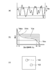
- FIG. 5 is a schematic diagram for explaining the three-dimensional surface property parameter.
- FIG. 5A is a graph illustrating the amplitude average (arithmetic average) Sa in the height direction.
- FIG. 5B is a graph illustrating the substantial volume Vmc of the core part and the hollow volume Vvc of the core part.
- FIG. 5C is a schematic plan view for explaining the density of protrusions (or holes) in the defined segmentation.
- the inventor examined the surface state of the layered structure using a laser microscope.
- As the laser microscope “OLS4000 / manufactured by Olympus” was used.
- the magnification of the objective lens is 100 times.
- the zoom is 5 times.
- the cut-off was set to 2.5 ⁇ m or 0.8 ⁇ m.
- the amplitude average (arithmetic mean) Sa in the height direction is obtained by extending the two-dimensional arithmetic average roughness Ra to three dimensions, and is a three-dimensional roughness parameter (three-dimensional height direction parameter). Specifically, the arithmetic average Sa is obtained by dividing the volume of the portion surrounded by the surface shape curved surface and the average surface by the measurement area.
- the arithmetic mean Sa is defined by the following equation.
- “A” in Equation (2) is a measurement area.
- Parameters relating to the substantial volume Vmc of the core portion and the hollow volume Vvc of the core portion obtained from the load curve are defined as a graph shown in FIG. 5B, and are three-dimensional volume parameters. That is, the height when the load area ratio is 10% is a boundary between the substantial volume Vmp of the mountain part, the substantial volume Vmc of the core part, and the hollow volume Vvc of the core part. The height when the load area ratio is 80% is a boundary between the hollow volume Vvv of the valley part, the substantial volume Vmc of the core part, and the hollow volume Vvc of the core part.
- the substantial volume Vmp of the peak part, the substantial volume Vmc of the core part, the hollow volume Vvc of the core part, and the hollow volume Vvv of the valley part represent a volume per unit area (unit: m 3 / m 2 ).
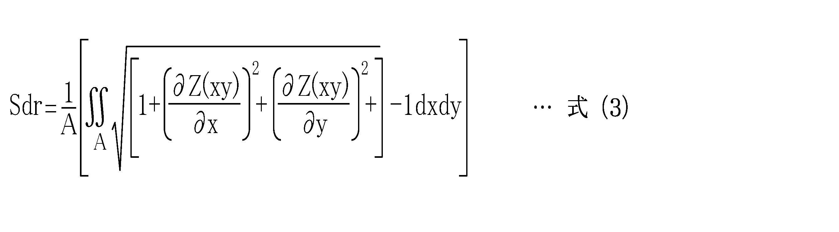
- the developed area ratio Sdr of the interface is a parameter indicating the increase rate of the interface with respect to the sampling surface.
- the developed area ratio Sdr of the interface is a value obtained by dividing the total developed area of the small interfaces formed by four points by the measured area, and is defined by the following equation.
- A in equation (3) represents the defined segmentation area.
- the root mean square slope S ⁇ q represents a two-dimensional mean square slope angle ⁇ q on the sampling surface. At every point, the surface slope is expressed as:
Landscapes
- Chemical & Material Sciences (AREA)
- Engineering & Computer Science (AREA)
- Organic Chemistry (AREA)
- Chemical Kinetics & Catalysis (AREA)
- Materials Engineering (AREA)
- Mechanical Engineering (AREA)
- Metallurgy (AREA)
- Plasma & Fusion (AREA)
- Physics & Mathematics (AREA)
- General Chemical & Material Sciences (AREA)
- Analytical Chemistry (AREA)
- Life Sciences & Earth Sciences (AREA)
- Geology (AREA)
- Inorganic Chemistry (AREA)
- Drying Of Semiconductors (AREA)
- Crystallography & Structural Chemistry (AREA)
- Chemical Vapour Deposition (AREA)
- Container, Conveyance, Adherence, Positioning, Of Wafer (AREA)
Abstract
Description
図1は、本発明の実施の形態にかかる耐プラズマ性部材を備えた半導体製造装置を表す模式的断面図である。
図1に表した半導体製造装置100は、チャンバー110と、耐プラズマ性部材120と、静電チャック160と、を備える。耐プラズマ性部材120は、例えば天板などと呼ばれ、チャンバー110の内部における上部に設けられている。静電チャック160は、チャンバー110の内部における下部に設けられている。つまり、耐プラズマ性部材120は、チャンバー110の内部において静電チャック160の上に設けられている。ウェーハ210等の被吸着物は、静電チャック160の上に載置される。
なお、本願明細書において「常温」とは、セラミックスの焼結温度に対して著しく低い温度で、実質的には0~100℃の室温環境をいう。
なお、本願明細書において「粉体」とは、前述した微粒子が自然凝集した状態をいう。
ここで、緻密度(%)は、文献値または理論計算値による真比重と、層状構造物123の質量および体積から求めた嵩比重と、を用いて、(嵩比重÷真比重)×100(%)の式から算出される。また、層状構造物123の重量または体積の測定が困難な場合には、例えば走査型電子顕微鏡(Scanning Electron Microscope:SEM)などを用いて断面観察を行い、層状構造物中のポア部の体積を3次元画像解析から求め、緻密度を算出してもよい。
以下、本実施形態の耐プラズマ性部材120の表面に形成された層状構造物123について、図面を参照しつつ説明する。
本願明細書において「加熱処理」とは、乾燥器、オーブン、焼成炉、レーザー、電子ビーム、イオンビーム、分子ビーム、原子ビーム、高周波、プラズマなどを用いて物体を加熱処理することを言う。
また、本願明細書において「化学的処理」とは、水溶液中で水素イオンを生成するものを用いて物体の表面を処理することをいう。例えば、化学的処理としては、臭化水素酸、ヨウ化水素酸、次亜塩素酸、亜塩素酸、塩素酸、過塩素酸、硫酸、フルオロスルホン酸、硝酸、塩酸、リン酸、ヘキサフルオロアンチモン酸、テトラフルオロホウ酸、ヘキサフルオロリン酸、クロム酸、ホウ酸、メタンスルホン酸、エタンスルホン酸、ベンゼンスルホン酸、p-トルエンスルホン酸、トリフルオロメタンスルホン酸、ポリスチレンスルホン酸、酢酸、クエン酸、ギ酸、グルコン酸、乳酸、シュウ酸、酒石酸、フッ化水素酸、炭酸および硫化水素の少なくともいずれかを含む水溶液を用いた表面処理が挙げられる。
あるいは、本願明細書において「化学的処理」とは、水溶液中で水酸化物イオンを生成するものを用いて物体の表面を処理することをいう。例えば、化学的処理としては、水酸化ナトリウム、水酸化カリウム、アンモニア、水酸化カルシウム、水酸化バリウム、水酸化銅、水酸化アルミニウムおよび水酸化鉄の少なくともいずれかを含む水溶液を用いた表面処理が挙げられる。
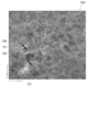
そして、本発明者は、加熱処理を施した後、化学的処理を施した層状構造物123の表面を観察した。その写真図は図2に示した通りである。
尚、本発明は、層状構造物123の表面を粗面化した場合に限定されるものではなく、製膜直後のアズデポジションの場合であっても、製膜後に研磨処理を施した場合であっても適用される。
本願発明者は、エアロゾルデポジション法により形成された後に加熱処理が施された層状構造物123について、結晶構造および耐薬品性の評価を行った。図3には、加熱処理の条件の一例として、200℃、300℃、350℃、400℃及び600℃を示している。加熱時間は、例えば2時間程度である。
また、比較例として、エアロゾルデポジション法により形成された後に加熱処理が施されない層状構造物についても、同様に結晶構造及び耐薬品性の評価を行った。
耐薬品性の評価として、層状構造物123を化学洗浄した後の、層状構造物123の表面粗さのばらつきの大きさを「大」「中」「小」に分類した。
各熱処理の条件ごとに、各評価項目において複数の測定点を測定した。図3は、層状構造物123中のイットリア多結晶体における、各評価項目の平均値や標準偏差を示す。
以上の評価方法の詳細については、後述する。
このように、エアロゾルデポジション法により形成された後に加熱処理が施されない層状構造物においては、イットリア多結晶の結晶構造のばらつきが比較的大きい。
図4は、耐プラズマ性部材の表面に形成された層状構造物を例示する写真図である。図4の例では、上述の200℃の加熱処理を施したイットリア多結晶体を、集束イオンビーム(FIB)法を用いて薄片化して観察した。観察においては、透過型電子顕微鏡(H-9000NAR/日立テクノロジーズ製)を用い、加速電圧を300kVとした。透過型電子顕微鏡像において、イットリア多結晶体中の互いに隣接する結晶子125同士の間隔G1は、0nm以上10nm未満であった。例えば、観察した画像中において間隔G1の平均値は、0nm以上10nm未満である。
加熱処理が施されていない比較例においては、原子数濃度比(O/Y)が1.9~2.2である。これに対して、加熱処理によって原子数濃度が低下している。これは、例えば、加熱処理によってOH基を介した脱水結合が生じたためと考えられる。これにより、イットリア粒子がより強固に結合し、より緻密な構造が得られ、耐薬品性が向上する。
結晶子サイズ、立方晶に対する単斜晶の割合および格子歪み、の測定には、X線回折(X-ray Diffraction:XRD)を用いた。
D=Kλ/(βcosθ)
ここで、Dは結晶子サイズであり、βはピーク半値幅(ラジアン(rad))であり、θはブラッグ角(rad)であり、λは測定に用いたX線の波長である。
シェラーの式において、βは、β=(βobs-βstd)により算出される。βobsは、測定試料のX線回折ピークの半値幅であり、βstdは、標準試料のX線回折ピークの半値幅である。Kの値として0.94を用いた。
格子歪みの算出には、2θ=48°近傍のピークを用いて、以下のウィルソンの式を使用した。
d=β/(4tanθ)
ここで、dは、格子歪みである。βはピーク半値幅(rad)であり、βはピーク半値幅(rad)であり、θはブラッグ角(rad)である。ウィルソンの式においては、βは、β=(βobs 2-βstd 2)1/2により算出される。βobsは、測定試料のX線回折ピークの半値幅であり、βstdは、標準試料のX線回折ピークの半値幅である。
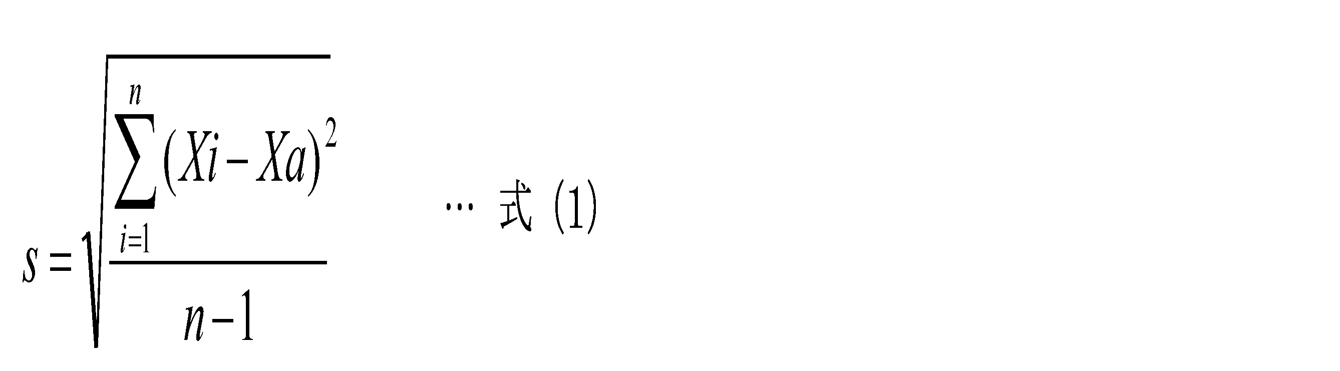
sは標準偏差、nは測定点の数、Xiは、各測定点における測定値(立方晶に対する単斜晶の割合、結晶子サイズまたは格子歪み)、Xaは、複数の測定点の平均値である。なお、各値(平均値又は標準偏差)の算出に用いられる測定点の数nは、3以上である。熱処理の各条件における複数の測定点は、1つの耐プラズマ性部材から選択されてもよく、同一の条件で形成された異なる耐プラズマ性部材から選択されてもよい。
図5は、3次元表面性状パラメータを説明する模式図である。なお、図5(a)は、高さ方向の振幅平均(算術平均)Saを説明するグラフ図である。図5(b)は、コア部の実体体積Vmcおよびコア部の中空体積Vvcを説明するグラフ図である。図5(c)は、定義したセグメンテーション内での突起(あるいは穴)密度を説明する模式的平面図である。

負荷曲線から求めるコア部の実体体積Vmcおよびコア部の中空体積Vvcに関するパラメータは、図5(b)に表したグラフ図のように定義され、3次元体積パラメータである。すなわち、負荷面積率が10%のときの高さが、山部の実体体積Vmpと、コア部の実体体積Vmcおよびコア部の中空体積Vvcと、の境界となる。負荷面積率が80%のときの高さが、谷部の中空体積Vvvと、コア部の実体体積Vmcおよびコア部の中空体積Vvcと、の境界となる。山部の実体体積Vmp、コア部の実体体積Vmc、コア部の中空体積Vvcおよび谷部の中空体積Vvvは、単位面積あたりの体積(単位:m3/m2)を表す。
二乗平均平方根傾斜SΔqは、サンプリング面での二次元の二乗平均傾斜角Δqを表す。あらゆる点において、表面傾斜は、次式で表される。

したがって、二乗平均平方根傾斜SΔqは、次式で表される。

以上、本発明の実施の形態について説明した。しかし、本発明はこれらの記述に限定されるものではない。前述の実施の形態に関して、当業者が適宜設計変更を加えたものも、本発明の特徴を備えている限り、本発明の範囲に包含される。例えば、半導体製造装置100などが備える各要素の形状、寸法、材質、配置などや耐プラズマ性部材120および静電チャック160の設置形態などは、例示したものに限定されるわけではなく適宜変更することができる。
また、前述した各実施の形態が備える各要素は、技術的に可能な限りにおいて組み合わせることができ、これらを組み合わせたものも本発明の特徴を含む限り本発明の範囲に包含される。
110 チャンバー、
120 耐プラズマ性部材、
123 層状構造物、
125 結晶子、
160 静電チャック、
191 領域、
210 ウェーハ、
221 パーティクル
Claims (8)
- 基材と、
前記基材の表面に形成されイットリア多結晶体を含み耐プラズマ性を有する層状構造物と、
を備え、
前記層状構造物を構成するイットリア多結晶体に含まれる結晶子同士は、異相を介して接合されておらず、
前記層状構造物を構成するイットリア多結晶体は、立方晶のみを含む結晶構造または立方晶と単斜晶とが混在した結晶構造を有し、
前記層状構造物を構成するイットリア多結晶体中における、立方晶に対する単斜晶の割合の平均値は、0%より大きく60%以下であることを特徴とする耐プラズマ性部材。 - 前記層状構造物を構成するイットリア多結晶体における、立方晶に対する単斜晶の前記割合の分布の標準偏差は、0%以上15%以下であることを特徴とする請求項1に記載の耐プラズマ性部材。
- 基材と、
前記基材の表面に形成されイットリア多結晶体を含み耐プラズマ性を有する層状構造物と、
を備え、
前記層状構造物を構成するイットリア多結晶体に含まれる結晶子同士は、異相を介して接合されておらず、
前記層状構造物を構成するイットリア多結晶体は、立方晶のみを含む結晶構造または立方晶と単斜晶とが混在した結晶構造を有し、
前記層状構造物を構成するイットリア多結晶体中における、立方晶に対する単斜晶の割合の平均値は、25%以下であることを特徴とする耐プラズマ性部材。 - 前記層状構造物を構成するイットリア多結晶体の平均結晶子サイズは、12ナノメートル以上40ナノメートル以下であることを特徴とする請求項1~3のいずれか1つに記載の耐プラズマ性部材。
- 前記層状構造物を構成するイットリア多結晶体の結晶子サイズの分布の標準偏差は、0.1ナノメートル以上1.1ナノメートル以下であることを特徴とする請求項4に記載の耐プラズマ性部材。
- 前記層状構造物を構成するイットリア多結晶体の平均格子歪みは、0.2%以上0.5%以下であることを特徴とする請求項1~5のいずれか1つに記載の耐プラズマ性部材。
- 前記層状構造物を構成するイットリア多結晶体の格子歪みの分布の標準偏差は、0.003%以上0.04%以下であることを特徴とする請求項6に記載の耐プラズマ性部材。
- 前記層状構造物を構成するイットリア多結晶体中における、イットリウム(Y)の原子数濃度に対する酸素(O)の原子数濃度の比(O/Y)は、1.3以上1.8以下であることを特徴とする請求項1~7のいずれか1つに記載の耐プラズマ性部材。
Priority Applications (4)
| Application Number | Priority Date | Filing Date | Title |
|---|---|---|---|
| KR1020187016450A KR102087058B1 (ko) | 2015-12-24 | 2015-12-25 | 내플라즈마성 부재 |
| KR1020197035509A KR102213487B1 (ko) | 2015-12-24 | 2015-12-25 | 내플라즈마성 부재 |
| CN201580085291.1A CN108431299B (zh) | 2015-12-24 | 2015-12-25 | 耐等离子体性部件 |
| US16/015,832 US11127569B2 (en) | 2015-12-24 | 2018-06-22 | Plasma-resistant member |
Applications Claiming Priority (2)
| Application Number | Priority Date | Filing Date | Title |
|---|---|---|---|
| JP2015251873A JP6808168B2 (ja) | 2015-12-24 | 2015-12-24 | 耐プラズマ性部材 |
| JP2015-251873 | 2015-12-24 |
Related Child Applications (1)
| Application Number | Title | Priority Date | Filing Date |
|---|---|---|---|
| US16/015,832 Continuation US11127569B2 (en) | 2015-12-24 | 2018-06-22 | Plasma-resistant member |
Publications (1)
| Publication Number | Publication Date |
|---|---|
| WO2017109975A1 true WO2017109975A1 (ja) | 2017-06-29 |
Family
ID=59089751
Family Applications (1)
| Application Number | Title | Priority Date | Filing Date |
|---|---|---|---|
| PCT/JP2015/086337 Ceased WO2017109975A1 (ja) | 2015-12-24 | 2015-12-25 | 耐プラズマ性部材 |
Country Status (6)
| Country | Link |
|---|---|
| US (1) | US11127569B2 (ja) |
| JP (1) | JP6808168B2 (ja) |
| KR (2) | KR102087058B1 (ja) |
| CN (1) | CN108431299B (ja) |
| TW (1) | TWI606933B (ja) |
| WO (1) | WO2017109975A1 (ja) |
Cited By (5)
| Publication number | Priority date | Publication date | Assignee | Title |
|---|---|---|---|---|
| JP2020012192A (ja) * | 2018-03-08 | 2020-01-23 | Toto株式会社 | 複合構造物および複合構造物を備えた半導体製造装置並びにディスプレイ製造装置 |
| JP2020084287A (ja) * | 2018-11-29 | 2020-06-04 | 日本特殊陶業株式会社 | 膜付き部材及びその製造方法、並びに膜付き部材の評価方法 |
| US10759710B2 (en) | 2018-03-08 | 2020-09-01 | Toto Ltd. | Composite structure, semiconductor manufacturing apparatus and display manufacturing apparatus provided with composite structure |
| JPWO2021220943A1 (ja) * | 2020-04-27 | 2021-11-04 | ||
| JPWO2022092022A1 (ja) * | 2020-10-28 | 2022-05-05 |
Families Citing this family (7)
| Publication number | Priority date | Publication date | Assignee | Title |
|---|---|---|---|---|
| US11087961B2 (en) * | 2018-03-02 | 2021-08-10 | Lam Research Corporation | Quartz component with protective coating |
| JP7627992B2 (ja) * | 2019-11-01 | 2025-02-07 | 日本特殊陶業株式会社 | 溶射膜被覆部材の製造方法および溶射膜被覆部材 |
| JP7197036B2 (ja) * | 2021-04-21 | 2022-12-27 | Toto株式会社 | 半導体製造装置用部材及び半導体製造装置 |
| US11749507B2 (en) | 2021-04-21 | 2023-09-05 | Toto Ltd. | Semiconductor manufacturing apparatus member and semiconductor manufacturing apparatus |
| JP7679850B2 (ja) * | 2023-03-28 | 2025-05-20 | Toto株式会社 | 構造部材 |
| JP7776032B2 (ja) * | 2024-03-28 | 2025-11-26 | Toto株式会社 | 構造部材 |
| JP7747237B1 (ja) | 2024-03-28 | 2025-10-01 | Toto株式会社 | 構造部材 |
Citations (5)
| Publication number | Priority date | Publication date | Assignee | Title |
|---|---|---|---|---|
| JP2006089338A (ja) * | 2004-09-24 | 2006-04-06 | Kyocera Corp | 耐食性部材とその製造方法、およびこれを用いた半導体・液晶製造装置用部材 |
| JP2007131943A (ja) * | 2005-10-12 | 2007-05-31 | Toto Ltd | 複合構造物 |
| WO2013099890A1 (ja) * | 2011-12-28 | 2013-07-04 | 株式会社 フジミインコーポレーテッド | 酸化イットリウム皮膜 |
| WO2013176168A1 (ja) * | 2012-05-22 | 2013-11-28 | 株式会社東芝 | プラズマ処理装置用部品およびプラズマ処理装置用部品の製造方法 |
| JP2016027624A (ja) * | 2014-06-26 | 2016-02-18 | Toto株式会社 | 耐プラズマ性部材及びその製造方法 |
Family Cites Families (6)
| Publication number | Priority date | Publication date | Assignee | Title |
|---|---|---|---|---|
| JP3251215B2 (ja) | 1996-10-02 | 2002-01-28 | 松下電器産業株式会社 | 電子デバイスの製造装置及び電子デバイスの製造方法 |
| JP2005060827A (ja) * | 2003-07-29 | 2005-03-10 | Toshiba Ceramics Co Ltd | 耐プラズマ部材 |
| JP3864958B2 (ja) | 2004-02-02 | 2007-01-10 | 東陶機器株式会社 | 耐プラズマ性を有する半導体製造装置用部材およびその作製方法 |
| JP2007115973A (ja) * | 2005-10-21 | 2007-05-10 | Shin Etsu Chem Co Ltd | 耐食性部材 |
| KR101094725B1 (ko) * | 2011-06-24 | 2011-12-16 | 주식회사 펨빅스 | 산화이트륨 코팅막 및 산화이트륨 코팅방법 |
| CN103449816B (zh) * | 2013-08-06 | 2015-02-11 | 施丽萍 | 一种耐等离子腐蚀热喷涂用造粒氧化钇及其制备方法 |
-
2015
- 2015-12-24 JP JP2015251873A patent/JP6808168B2/ja active Active
- 2015-12-25 KR KR1020187016450A patent/KR102087058B1/ko not_active Expired - Fee Related
- 2015-12-25 TW TW104143687A patent/TWI606933B/zh active
- 2015-12-25 KR KR1020197035509A patent/KR102213487B1/ko active Active
- 2015-12-25 CN CN201580085291.1A patent/CN108431299B/zh active Active
- 2015-12-25 WO PCT/JP2015/086337 patent/WO2017109975A1/ja not_active Ceased
-
2018
- 2018-06-22 US US16/015,832 patent/US11127569B2/en active Active
Patent Citations (5)
| Publication number | Priority date | Publication date | Assignee | Title |
|---|---|---|---|---|
| JP2006089338A (ja) * | 2004-09-24 | 2006-04-06 | Kyocera Corp | 耐食性部材とその製造方法、およびこれを用いた半導体・液晶製造装置用部材 |
| JP2007131943A (ja) * | 2005-10-12 | 2007-05-31 | Toto Ltd | 複合構造物 |
| WO2013099890A1 (ja) * | 2011-12-28 | 2013-07-04 | 株式会社 フジミインコーポレーテッド | 酸化イットリウム皮膜 |
| WO2013176168A1 (ja) * | 2012-05-22 | 2013-11-28 | 株式会社東芝 | プラズマ処理装置用部品およびプラズマ処理装置用部品の製造方法 |
| JP2016027624A (ja) * | 2014-06-26 | 2016-02-18 | Toto株式会社 | 耐プラズマ性部材及びその製造方法 |
Cited By (9)
| Publication number | Priority date | Publication date | Assignee | Title |
|---|---|---|---|---|
| JP2020012192A (ja) * | 2018-03-08 | 2020-01-23 | Toto株式会社 | 複合構造物および複合構造物を備えた半導体製造装置並びにディスプレイ製造装置 |
| US10759710B2 (en) | 2018-03-08 | 2020-09-01 | Toto Ltd. | Composite structure, semiconductor manufacturing apparatus and display manufacturing apparatus provided with composite structure |
| JP2020084287A (ja) * | 2018-11-29 | 2020-06-04 | 日本特殊陶業株式会社 | 膜付き部材及びその製造方法、並びに膜付き部材の評価方法 |
| JPWO2021220943A1 (ja) * | 2020-04-27 | 2021-11-04 | ||
| WO2021220943A1 (ja) * | 2020-04-27 | 2021-11-04 | 京セラ株式会社 | 通気性部材、半導体製造装置用部材、プラグおよび吸着部材 |
| JP7397974B2 (ja) | 2020-04-27 | 2023-12-13 | 京セラ株式会社 | 通気性部材、半導体製造装置用部材、プラグおよび吸着部材 |
| JPWO2022092022A1 (ja) * | 2020-10-28 | 2022-05-05 | ||
| WO2022092022A1 (ja) * | 2020-10-28 | 2022-05-05 | 京セラ株式会社 | ギャップピン |
| JP7398011B2 (ja) | 2020-10-28 | 2023-12-13 | 京セラ株式会社 | ギャップピン |
Also Published As
| Publication number | Publication date |
|---|---|
| JP6808168B2 (ja) | 2021-01-06 |
| US11127569B2 (en) | 2021-09-21 |
| JP2017114724A (ja) | 2017-06-29 |
| TW201722715A (zh) | 2017-07-01 |
| CN108431299A (zh) | 2018-08-21 |
| KR20180084876A (ko) | 2018-07-25 |
| TWI606933B (zh) | 2017-12-01 |
| KR20190135576A (ko) | 2019-12-06 |
| US20180301321A1 (en) | 2018-10-18 |
| CN108431299B (zh) | 2020-11-06 |
| KR102213487B1 (ko) | 2021-02-08 |
| KR102087058B1 (ko) | 2020-04-23 |
Similar Documents
| Publication | Publication Date | Title |
|---|---|---|
| JP5888458B2 (ja) | 耐プラズマ性部材及びその製造方法 | |
| JP6808168B2 (ja) | 耐プラズマ性部材 | |
| JP5578383B2 (ja) | 耐プラズマ性部材 | |
| KR102499540B1 (ko) | 반도체 제조 장치용 부재, 및 반도체 제조 장치용 부재를 구비한 반도체 제조 장치, 및 디스플레이 제조 장치 | |
| JP2016102264A (ja) | 耐プラズマ性部材 | |
| KR20200104810A (ko) | 반도체 제조 장치용 부재, 및 반도체 제조 장치용 부재를 구비한 반도체 제조 장치, 및 디스플레이 제조 장치 | |
| JP2016008352A (ja) | 耐プラズマ性部材 | |
| JP6358492B2 (ja) | 耐プラズマ性部材 | |
| JP7841273B2 (ja) | 複合構造物および複合構造物を備えた半導体製造装置 | |
| CN113582678B (zh) | 复合结构物以及具备复合结构物的半导体制造装置 | |
| KR102542911B1 (ko) | 복합 구조물 및 복합 구조물을 구비한 반도체 제조 장치 | |
| CN116917544A (zh) | 复合结构物以及具备复合结构物的半导体制造装置 | |
| JP2023124884A (ja) | 複合構造物および複合構造物を備えた半導体製造装置 | |
| KR20230146583A (ko) | 복합 구조물 및 복합 구조물을 구비한 반도체 제조 장치 | |
| JP2023124887A (ja) | 複合構造物および複合構造物を備えた半導体製造装置 | |
| KR20230146584A (ko) | 복합 구조물 및 복합 구조물을 구비한 반도체 제조 장치 | |
| JP2023124888A (ja) | 複合構造物および複合構造物を備えた半導体製造装置 | |
| JP2023124889A (ja) | 複合構造物および複合構造物を備えた半導体製造装置 | |
| CN116868316A (zh) | 复合结构物以及具备复合结构物的半导体制造装置 |
Legal Events
| Date | Code | Title | Description |
|---|---|---|---|
| 121 | Ep: the epo has been informed by wipo that ep was designated in this application |
Ref document number: 15911409 Country of ref document: EP Kind code of ref document: A1 |
|
| ENP | Entry into the national phase |
Ref document number: 20187016450 Country of ref document: KR Kind code of ref document: A |
|
| WWE | Wipo information: entry into national phase |
Ref document number: 1020187016450 Country of ref document: KR |
|
| NENP | Non-entry into the national phase |
Ref country code: DE |
|
| 122 | Ep: pct application non-entry in european phase |
Ref document number: 15911409 Country of ref document: EP Kind code of ref document: A1 |