WO2017090584A1 - 薄膜トランジスタ、酸化物半導体膜及びスパッタリングターゲット - Google Patents
薄膜トランジスタ、酸化物半導体膜及びスパッタリングターゲット Download PDFInfo
- Publication number
- WO2017090584A1 WO2017090584A1 PCT/JP2016/084539 JP2016084539W WO2017090584A1 WO 2017090584 A1 WO2017090584 A1 WO 2017090584A1 JP 2016084539 W JP2016084539 W JP 2016084539W WO 2017090584 A1 WO2017090584 A1 WO 2017090584A1
- Authority
- WO
- WIPO (PCT)
- Prior art keywords
- atomic
- film
- oxide semiconductor
- active layer
- ratio
- Prior art date
- Legal status (The legal status is an assumption and is not a legal conclusion. Google has not performed a legal analysis and makes no representation as to the accuracy of the status listed.)
- Ceased
Links
Images




Classifications
-
- H—ELECTRICITY
- H10—SEMICONDUCTOR DEVICES; ELECTRIC SOLID-STATE DEVICES NOT OTHERWISE PROVIDED FOR
- H10D—INORGANIC ELECTRIC SEMICONDUCTOR DEVICES
- H10D30/00—Field-effect transistors [FET]
- H10D30/60—Insulated-gate field-effect transistors [IGFET]
- H10D30/67—Thin-film transistors [TFT]
- H10D30/674—Thin-film transistors [TFT] characterised by the active materials
- H10D30/6755—Oxide semiconductors, e.g. zinc oxide, copper aluminium oxide or cadmium stannate
-
- C—CHEMISTRY; METALLURGY
- C23—COATING METALLIC MATERIAL; COATING MATERIAL WITH METALLIC MATERIAL; CHEMICAL SURFACE TREATMENT; DIFFUSION TREATMENT OF METALLIC MATERIAL; COATING BY VACUUM EVAPORATION, BY SPUTTERING, BY ION IMPLANTATION OR BY CHEMICAL VAPOUR DEPOSITION, IN GENERAL; INHIBITING CORROSION OF METALLIC MATERIAL OR INCRUSTATION IN GENERAL
- C23C—COATING METALLIC MATERIAL; COATING MATERIAL WITH METALLIC MATERIAL; SURFACE TREATMENT OF METALLIC MATERIAL BY DIFFUSION INTO THE SURFACE, BY CHEMICAL CONVERSION OR SUBSTITUTION; COATING BY VACUUM EVAPORATION, BY SPUTTERING, BY ION IMPLANTATION OR BY CHEMICAL VAPOUR DEPOSITION, IN GENERAL
- C23C14/00—Coating by vacuum evaporation, by sputtering or by ion implantation of the coating forming material
- C23C14/06—Coating by vacuum evaporation, by sputtering or by ion implantation of the coating forming material characterised by the coating material
- C23C14/08—Oxides
-
- C—CHEMISTRY; METALLURGY
- C23—COATING METALLIC MATERIAL; COATING MATERIAL WITH METALLIC MATERIAL; CHEMICAL SURFACE TREATMENT; DIFFUSION TREATMENT OF METALLIC MATERIAL; COATING BY VACUUM EVAPORATION, BY SPUTTERING, BY ION IMPLANTATION OR BY CHEMICAL VAPOUR DEPOSITION, IN GENERAL; INHIBITING CORROSION OF METALLIC MATERIAL OR INCRUSTATION IN GENERAL
- C23C—COATING METALLIC MATERIAL; COATING MATERIAL WITH METALLIC MATERIAL; SURFACE TREATMENT OF METALLIC MATERIAL BY DIFFUSION INTO THE SURFACE, BY CHEMICAL CONVERSION OR SUBSTITUTION; COATING BY VACUUM EVAPORATION, BY SPUTTERING, BY ION IMPLANTATION OR BY CHEMICAL VAPOUR DEPOSITION, IN GENERAL
- C23C14/00—Coating by vacuum evaporation, by sputtering or by ion implantation of the coating forming material
- C23C14/06—Coating by vacuum evaporation, by sputtering or by ion implantation of the coating forming material characterised by the coating material
- C23C14/08—Oxides
- C23C14/083—Oxides of refractory metals or yttrium
-
- C—CHEMISTRY; METALLURGY
- C23—COATING METALLIC MATERIAL; COATING MATERIAL WITH METALLIC MATERIAL; CHEMICAL SURFACE TREATMENT; DIFFUSION TREATMENT OF METALLIC MATERIAL; COATING BY VACUUM EVAPORATION, BY SPUTTERING, BY ION IMPLANTATION OR BY CHEMICAL VAPOUR DEPOSITION, IN GENERAL; INHIBITING CORROSION OF METALLIC MATERIAL OR INCRUSTATION IN GENERAL
- C23C—COATING METALLIC MATERIAL; COATING MATERIAL WITH METALLIC MATERIAL; SURFACE TREATMENT OF METALLIC MATERIAL BY DIFFUSION INTO THE SURFACE, BY CHEMICAL CONVERSION OR SUBSTITUTION; COATING BY VACUUM EVAPORATION, BY SPUTTERING, BY ION IMPLANTATION OR BY CHEMICAL VAPOUR DEPOSITION, IN GENERAL
- C23C14/00—Coating by vacuum evaporation, by sputtering or by ion implantation of the coating forming material
- C23C14/06—Coating by vacuum evaporation, by sputtering or by ion implantation of the coating forming material characterised by the coating material
- C23C14/08—Oxides
- C23C14/086—Oxides of zinc, germanium, cadmium, indium, tin, thallium or bismuth
-
- C—CHEMISTRY; METALLURGY
- C23—COATING METALLIC MATERIAL; COATING MATERIAL WITH METALLIC MATERIAL; CHEMICAL SURFACE TREATMENT; DIFFUSION TREATMENT OF METALLIC MATERIAL; COATING BY VACUUM EVAPORATION, BY SPUTTERING, BY ION IMPLANTATION OR BY CHEMICAL VAPOUR DEPOSITION, IN GENERAL; INHIBITING CORROSION OF METALLIC MATERIAL OR INCRUSTATION IN GENERAL
- C23C—COATING METALLIC MATERIAL; COATING MATERIAL WITH METALLIC MATERIAL; SURFACE TREATMENT OF METALLIC MATERIAL BY DIFFUSION INTO THE SURFACE, BY CHEMICAL CONVERSION OR SUBSTITUTION; COATING BY VACUUM EVAPORATION, BY SPUTTERING, BY ION IMPLANTATION OR BY CHEMICAL VAPOUR DEPOSITION, IN GENERAL
- C23C14/00—Coating by vacuum evaporation, by sputtering or by ion implantation of the coating forming material
- C23C14/22—Coating by vacuum evaporation, by sputtering or by ion implantation of the coating forming material characterised by the process of coating
- C23C14/34—Sputtering
-
- C—CHEMISTRY; METALLURGY
- C23—COATING METALLIC MATERIAL; COATING MATERIAL WITH METALLIC MATERIAL; CHEMICAL SURFACE TREATMENT; DIFFUSION TREATMENT OF METALLIC MATERIAL; COATING BY VACUUM EVAPORATION, BY SPUTTERING, BY ION IMPLANTATION OR BY CHEMICAL VAPOUR DEPOSITION, IN GENERAL; INHIBITING CORROSION OF METALLIC MATERIAL OR INCRUSTATION IN GENERAL
- C23C—COATING METALLIC MATERIAL; COATING MATERIAL WITH METALLIC MATERIAL; SURFACE TREATMENT OF METALLIC MATERIAL BY DIFFUSION INTO THE SURFACE, BY CHEMICAL CONVERSION OR SUBSTITUTION; COATING BY VACUUM EVAPORATION, BY SPUTTERING, BY ION IMPLANTATION OR BY CHEMICAL VAPOUR DEPOSITION, IN GENERAL
- C23C14/00—Coating by vacuum evaporation, by sputtering or by ion implantation of the coating forming material
- C23C14/22—Coating by vacuum evaporation, by sputtering or by ion implantation of the coating forming material characterised by the process of coating
- C23C14/34—Sputtering
- C23C14/3407—Cathode assembly for sputtering apparatus, e.g. Target
- C23C14/3414—Metallurgical or chemical aspects of target preparation, e.g. casting, powder metallurgy
-
- H—ELECTRICITY
- H01—ELECTRIC ELEMENTS
- H01J—ELECTRIC DISCHARGE TUBES OR DISCHARGE LAMPS
- H01J37/00—Discharge tubes with provision for introducing objects or material to be exposed to the discharge, e.g. for the purpose of examination or processing thereof
- H01J37/32—Gas-filled discharge tubes
- H01J37/34—Gas-filled discharge tubes operating with cathodic sputtering
- H01J37/3411—Constructional aspects of the reactor
- H01J37/3414—Targets
- H01J37/3426—Material
- H01J37/3429—Plural materials
-
- H—ELECTRICITY
- H10—SEMICONDUCTOR DEVICES; ELECTRIC SOLID-STATE DEVICES NOT OTHERWISE PROVIDED FOR
- H10D—INORGANIC ELECTRIC SEMICONDUCTOR DEVICES
- H10D30/00—Field-effect transistors [FET]
- H10D30/60—Insulated-gate field-effect transistors [IGFET]
- H10D30/67—Thin-film transistors [TFT]
- H10D30/6704—Thin-film transistors [TFT] having supplementary regions or layers in the thin films or in the insulated bulk substrates for controlling properties of the device
- H10D30/6713—Thin-film transistors [TFT] having supplementary regions or layers in the thin films or in the insulated bulk substrates for controlling properties of the device characterised by the properties of the source or drain regions, e.g. compositions or sectional shapes
-
- H—ELECTRICITY
- H10—SEMICONDUCTOR DEVICES; ELECTRIC SOLID-STATE DEVICES NOT OTHERWISE PROVIDED FOR
- H10D—INORGANIC ELECTRIC SEMICONDUCTOR DEVICES
- H10D99/00—Subject matter not provided for in other groups of this subclass
-
- H—ELECTRICITY
- H10—SEMICONDUCTOR DEVICES; ELECTRIC SOLID-STATE DEVICES NOT OTHERWISE PROVIDED FOR
- H10P—GENERIC PROCESSES OR APPARATUS FOR THE MANUFACTURE OR TREATMENT OF DEVICES COVERED BY CLASS H10
- H10P14/00—Formation of materials, e.g. in the shape of layers or pillars
- H10P14/20—Formation of materials, e.g. in the shape of layers or pillars of semiconductor materials
- H10P14/22—Formation of materials, e.g. in the shape of layers or pillars of semiconductor materials using physical deposition, e.g. vacuum deposition or sputtering
-
- H—ELECTRICITY
- H10—SEMICONDUCTOR DEVICES; ELECTRIC SOLID-STATE DEVICES NOT OTHERWISE PROVIDED FOR
- H10P—GENERIC PROCESSES OR APPARATUS FOR THE MANUFACTURE OR TREATMENT OF DEVICES COVERED BY CLASS H10
- H10P14/00—Formation of materials, e.g. in the shape of layers or pillars
- H10P14/20—Formation of materials, e.g. in the shape of layers or pillars of semiconductor materials
- H10P14/29—Formation of materials, e.g. in the shape of layers or pillars of semiconductor materials characterised by the substrates
- H10P14/2901—Materials
- H10P14/2922—Materials being non-crystalline insulating materials, e.g. glass or polymers
-
- H—ELECTRICITY
- H10—SEMICONDUCTOR DEVICES; ELECTRIC SOLID-STATE DEVICES NOT OTHERWISE PROVIDED FOR
- H10P—GENERIC PROCESSES OR APPARATUS FOR THE MANUFACTURE OR TREATMENT OF DEVICES COVERED BY CLASS H10
- H10P14/00—Formation of materials, e.g. in the shape of layers or pillars
- H10P14/20—Formation of materials, e.g. in the shape of layers or pillars of semiconductor materials
- H10P14/32—Formation of materials, e.g. in the shape of layers or pillars of semiconductor materials characterised by intermediate layers between substrates and deposited layers
- H10P14/3202—Materials thereof
- H10P14/3238—Materials thereof being insulating materials
-
- H—ELECTRICITY
- H10—SEMICONDUCTOR DEVICES; ELECTRIC SOLID-STATE DEVICES NOT OTHERWISE PROVIDED FOR
- H10P—GENERIC PROCESSES OR APPARATUS FOR THE MANUFACTURE OR TREATMENT OF DEVICES COVERED BY CLASS H10
- H10P14/00—Formation of materials, e.g. in the shape of layers or pillars
- H10P14/20—Formation of materials, e.g. in the shape of layers or pillars of semiconductor materials
- H10P14/34—Deposited materials, e.g. layers
- H10P14/3402—Deposited materials, e.g. layers characterised by the chemical composition
- H10P14/3424—Deposited materials, e.g. layers characterised by the chemical composition being Group IIB-VIA materials
- H10P14/3426—Oxides
-
- H—ELECTRICITY
- H10—SEMICONDUCTOR DEVICES; ELECTRIC SOLID-STATE DEVICES NOT OTHERWISE PROVIDED FOR
- H10P—GENERIC PROCESSES OR APPARATUS FOR THE MANUFACTURE OR TREATMENT OF DEVICES COVERED BY CLASS H10
- H10P14/00—Formation of materials, e.g. in the shape of layers or pillars
- H10P14/20—Formation of materials, e.g. in the shape of layers or pillars of semiconductor materials
- H10P14/34—Deposited materials, e.g. layers
- H10P14/3402—Deposited materials, e.g. layers characterised by the chemical composition
- H10P14/3434—Deposited materials, e.g. layers characterised by the chemical composition being oxide semiconductor materials
Definitions
- the present invention relates to a thin film transistor having an active layer made of an oxide semiconductor, an oxide semiconductor film, and a sputtering target.
- TFT Thin-Film Transistor
- IGZO In—Ga—Zn—O-based oxide semiconductor film
- Patent Document 1 discloses an organic EL display device in which an active layer of a TFT that drives an organic EL element is formed of IGZO.
- Patent Document 2 discloses a thin film transistor having a channel layer (active layer) made of a-IGZO and having a mobility of 5 cm 2 / Vs or more.
- Patent Document 3 discloses a thin film transistor having an active layer made of IGZO and an on / off current ratio of 5 digits or more.
- an object of the present invention is to provide a high-performance thin film transistor that replaces IGZO, an oxide semiconductor film used for an active layer thereof, and a sputtering target used for the film formation.
- a thin film transistor includes a gate electrode, an active layer including an oxide semiconductor film containing indium, zinc, and titanium, and between the gate electrode and the active layer. And a source electrode and a drain electrode electrically connected to the active layer.
- the thin film transistor uses an oxide semiconductor film in which an oxide containing indium and an oxide containing zinc to which an oxide containing titanium is added as an active layer.
- the atomic ratio of each element in the total amount of indium, zinc, and titanium constituting the oxide semiconductor film is as follows: indium is 24 atomic percent to 80 atomic percent, zinc is 16 atomic percent to 70 atomic percent, and titanium is 0 atomic percent. It may be 1 atomic% or more and 20 atomic% or less. Thereby, transistor characteristics having a mobility of 15 cm 2 / Vs or more and an on / off current ratio of 8 digits or more can be obtained.
- the atomic ratio of each of the above elements was 39.5 atomic% to 56.5 atomic% for indium, 39 atomic% to 56 atomic% for zinc, and 0.5 atomic% to 10 atomic% for titanium. May be. Accordingly, transistor characteristics having a mobility of 28 cm 2 / Vs or more and an on / off current ratio of 10 digits or more can be obtained.
- An oxide semiconductor film according to one embodiment of the present invention is formed using an oxide containing indium, zinc, and titanium.
- an active layer of a thin film transistor having transistor characteristics with a mobility of 15 cm 2 / Vs or more and an on / off current ratio of 8 digits or more can be formed.
- the atomic ratio of each element in the total amount of indium, zinc and titanium constituting the oxide is in the range of 24 atomic% to 80 atomic% indium, 16 atomic% to 70 atomic% in zinc, and 0.1 in titanium. Atom% or more and 20 atom% or less may be sufficient. Further, the atomic ratio of each of the above elements was 39.5 atomic% to 56.5 atomic% for indium, 39 atomic% to 56 atomic% for zinc, and 0.5 atomic% to 10 atomic% for titanium. May be.
- the oxide semiconductor film may have a carrier concentration of 1 ⁇ 10 18 / cm 3 or less. Thereby, transistor characteristics having a mobility of 15 cm 2 / Vs or more and an on / off current ratio of 8 digits or more can be obtained.
- a sputtering target includes a sintered body of oxides of indium, zinc, and titanium. Accordingly, an active layer of a thin film transistor having transistor characteristics with a mobility of 15 cm 2 / Vs or more and an on / off current ratio of 8 digits or more can be formed.
- the atomic ratio of each element in the total amount of indium, zinc and titanium constituting the sintered body is in the range of 24 atomic% to 80 atomic% for indium, 16 atomic% to 70 atomic% for zinc, and 0.2% for titanium. 1 atom% or more and 20 atom% or less may be sufficient. Further, the atomic ratio of each of the above elements was 39.5 atomic% to 56.5 atomic% for indium, 39 atomic% to 56 atomic% for zinc, and 0.5 atomic% to 10 atomic% for titanium. May be.
- an oxide semiconductor film used for an active layer of the thin film transistor can be provided.
- a sputtering target used for forming the oxide semiconductor film can be provided.
- FIG. 3 is a ternary phase diagram of —Ti.
- FIG. 1 is a schematic cross-sectional view showing a configuration of a thin film transistor according to an embodiment of the present invention.
- a so-called bottom gate type field effect transistor will be described as an example.
- the thin film transistor 1 of this embodiment includes a gate electrode 11, an active layer 15, a gate insulating film 14, a source electrode 17S, and a drain electrode 17D.
- the gate electrode 11 is made of a conductive film formed on the surface of the substrate 10.
- the substrate 10 is typically a transparent glass substrate.
- the gate electrode 11 is typically composed of a metal single layer film or a metal multilayer film such as molybdenum (Mo), titanium (Ti), aluminum (Al), or copper (Cu), and is formed by, for example, a sputtering method. .
- the gate electrode 11 is made of molybdenum.
- the thickness of the gate electrode 11 is not specifically limited, For example, it is 300 nm.
- the active layer 15 functions as a channel layer of the transistor 1.
- the film thickness of the active layer 15 is, for example, 30 nm to 200 nm.
- the active layer 15 includes an oxide semiconductor film containing indium (In), zinc (Zn), and titanium (Ti) (hereinafter also referred to as an In—Ti—Zn—O film).
- the atomic ratio of each element in the total amount of In, Zn, and Ti constituting the oxide semiconductor film is not particularly limited, and in this embodiment, In is 24 atomic% to 80 atomic% and Zn is 16 atomic%. 70 atomic% or less and Ti is 0.1 atomic% or more and 20 atomic% or less. Thereby, transistor characteristics having a mobility of 15 cm 2 / Vs or more and an on / off current ratio of 8 digits or more can be obtained.
- the atomic ratio of each of the above elements is 39.5 atomic% or more and 56.5 atomic% or less for In, 39 atomic% or more and 56 atomic% or less for Zn, and 0.5 atomic% or more and 10 atomic% or less for Ti.
- transistor characteristics having a mobility of 28 cm 2 / Vs or more and an on / off current ratio of 10 digits or more can be obtained.
- the carrier concentration of the oxide semiconductor film suitable as the active layer 15 is preferably 1 ⁇ 10 18 / cm 3 or less, for example. If the carrier concentration exceeds 1 ⁇ 10 18 / cm 3 , the on / off current ratio becomes 6 digits or less, and it may be difficult to obtain stable switching characteristics.
- the active layer 15 is formed using a sputtering target composed of a sintered body of oxides of In, Zn, and Ti, and then heat-treated (annealed) at a predetermined temperature. Is formed.
- a sputtering target composed of a sintered body of oxides of In, Zn, and Ti
- heat-treated (annealed) at a predetermined temperature Is formed.
- an oxide semiconductor film having the same or almost the same composition as the target is formed.
- annealing the semiconductor film at a predetermined temperature for example, an active layer that exhibits transistor characteristics with a mobility of 15 cm 2 / Vs or more and an on / off current ratio of 8 digits or more is formed.
- the gate insulating film 14 is formed between the gate electrode 11 and the active layer 15.
- the gate insulating film 14 is composed of a silicon oxide film (SiOx), a silicon nitride film (SiNx), or the like, but is not limited thereto, and can be formed using various electrical insulating films such as a metal oxide film.
- the film forming method is not particularly limited, and may be a CVD method, a sputtering method, a vapor deposition method, or the like.
- the thickness of the gate insulating film 14 is not particularly limited and is, for example, 200 nm to 400 nm.
- the source electrode 17S and the drain electrode 17D are formed on the active layer 15 so as to be separated from each other.
- the source electrode 17S and the drain electrode 17D can be composed of, for example, a metal single layer film such as aluminum, molybdenum, copper, titanium, or a multilayer film of these metals. As will be described later, the source electrode 17S and the drain electrode 17D can be simultaneously formed by patterning a metal film.
- the thickness of the metal film is, for example, 100 nm to 500 nm.
- An etching stopper layer 16 is formed on the active layer 15.
- the etching stopper layer 16 is provided to protect the active layer 15 from the etchant when pattern etching of the source electrode 17S and the drain electrode 17D is performed.
- the etching stopper layer 16 can be composed of, for example, a silicon oxide film, a silicon nitride film, or a laminated film thereof.
- the source electrode 17S and the drain electrode 17D are covered with a protective film 19.
- the protective film 19 is made of an electrically insulating material such as a silicon oxide film, a silicon nitride film, or a laminated film thereof.
- the protective film 19 is for shielding the element part including the active layer 15 from the outside air.
- the thickness of the protective film 19 is not particularly limited, and is, for example, 200 nm to 500 nm.
- the protective film 19 is provided with interlayer connection holes for connecting the source / drain electrodes 17S, 17D to the wiring layer 21 at appropriate positions.
- the wiring layer 21 is for connecting the transistor 1 to a peripheral circuit (not shown) and is made of a transparent conductive film such as ITO.
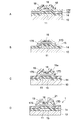
- FIG. 1 is a cross-sectional views of the main part of each step for explaining the method of manufacturing the thin film transistor 1.
- the gate electrode 11 is formed on one surface of the substrate 10.
- the gate electrode 11 is formed by patterning a gate electrode film formed on the surface of the substrate 10 into a predetermined shape.
- a gate insulating film 14 is formed on the surface of the base material 10 so as to cover the gate electrode 11.
- the thickness of the gate insulating film 14 is, for example, 200 nm to 500 nm.
- a thin film (hereinafter simply referred to as “In—Ti—Zn—O film”) 15F having an In—Ti—Zn—O-based composition is formed on the gate insulating film. .
- the In—Ti—Zn—O film 15F is formed by a sputtering method.
- a sputtering target a sintered body containing respective oxides of In, Zn, and Ti is used.
- the In—Ti—Zn—O film 15F is formed by sputtering this target in, for example, a mixed gas atmosphere of argon (Ar) and oxygen (O 2 ).
- Sputtering conditions are not particularly limited.
- the pressure (total pressure) in the film forming chamber is controlled within a range of 0.1 to 5 Pa.
- the substrate 10 may be formed in a state heated to a predetermined temperature, or may be formed in an unheated state, and the temperature of the substrate 10 is, for example, room temperature to 300 ° C. Under these conditions, the In—Ti—Zn—O film 15F is formed by pulse DC sputtering.
- the atmosphere during sputtering is not particularly limited, and sputtering may be performed in an atmosphere containing only argon without introducing oxygen.
- the sputtering discharge method is not limited to DC discharge, and may be AC discharge, RF discharge, or the like.
- the atomic ratio of each element occupying the total amount of In, Zn and Ti constituting the sintered body is not particularly limited.
- In is 24 atomic% or more and 80 atomic% or less
- Zn is 16 atomic%.
- 70 atomic% or less and Ti is 0.1 atomic% or more and 20 atomic% or less.
- the atomic ratio of each of the above elements is 39.5 atomic% or more and 56.5 atomic% or less for In, 39 atomic% or more and 56 atomic% or less for Zn, and 0.5 atomic% or more and 10 atomic% or less for Ti.
- transistor characteristics having a mobility of 28 cm 2 / Vs or more and an on / off current ratio of 10 digits or more can be obtained.
- the sputtering target may be composed of a sintered body obtained by mixing In, Zn, and Ti oxides such as In 2 O 3 , TiO 2, and ZnO as raw material powders, and mixing the raw material powders in the above composition ratio. it can.
- the obtained sputtered film has the same or almost the same composition as the target composition.
- an oxide semiconductor film formed by sputtering a target having a specified component ratio cannot obtain predetermined transistor characteristics. Therefore, as will be described in detail later, by annealing (heat treatment) the formed oxide semiconductor film within a predetermined temperature range, the structure relaxation of the oxide semiconductor film is promoted and the required transistor characteristics are exhibited. It becomes possible.
- an etching stopper layer 16 is formed on the In—Ti—Zn—O film 15F.
- the etching stopper layer 16 is formed of In-Ti-Zn-O in a patterning process of a metal film constituting a source electrode and a drain electrode, which will be described later, and in a process of etching away an unnecessary region of the In-Ti-Zn-O film 15F. It functions as an etching protective layer that protects the channel region of the film from the etchant.
- the etching stopper layer 16 is composed of, for example, a silicon oxide film, a silicon nitride film, or a laminated film thereof.
- the etching stopper layer 16 is formed, for example, by patterning a silicon oxide film formed on the In—Ti—Zn—O film 15F into a predetermined shape.
- the film thickness of the etching stopper layer 16 is not particularly limited, and is, for example, 30 nm to 300 nm.
- a metal film 17F is formed so as to cover the In—Ti—Zn—O film 15F and the etching stopper layer 16.
- the metal film 17F is typically composed of a metal single layer film or a metal multilayer film such as molybdenum, titanium, aluminum, or copper, and is formed by, for example, a sputtering method.
- the thickness of the metal film 17F is not particularly limited, and is, for example, 100 nm to 500 nm.
- the metal film 17F is patterned.
- the patterning process for the metal film 17F includes a process for forming the resist mask 18 and an etching process for the metal film 17F.
- the resist mask 18 has a mask pattern that opens the region immediately above the etching stopper layer 16 and the peripheral region of each transistor.
- the metal film 17F is etched by wet etching. As a result, the metal film 17F is separated into the source electrode 17S and the drain electrode 17D that are electrically connected to the active layer 15, respectively (FIG. 3B).
- the etching stopper layer 16 has a function of protecting the In—Ti—Zn—O film 15F from an etchant (for example, a mixed solution of phosphoric acid, nitric acid, and acetic acid) with respect to the metal film 17F.
- an etchant for example, a mixed solution of phosphoric acid, nitric acid, and acetic acid
- the etching stopper layer 16 is formed to cover a region (hereinafter referred to as “channel region”) located between the source electrode 17S and the drain electrode 17D of the In—Ti—Zn—O film 15F. . Therefore, the channel region of the In—Ti—Zn—O film 15F is not affected by the etching process of the metal film 17F.
- the In—Ti—Zn—O film 15F is etched using the resist mask 18 shown in FIG. 3A as a mask.
- the etching method is not particularly limited, and may be a wet etching method or a dry etching method.
- the In—Ti—Zn—O film 15F is isolated in element units, and the active layer 15 including the In—Ti—Zn—O film 15F is formed. Formed (FIG. 3B).
- the etching stopper layer 16 functions as an etching protective film for the In—Ti—Zn—O film 15F located in the channel region. That is, the etching stopper layer 16 has a function of protecting the channel region immediately below the etching stopper layer 16 from an etchant (for example, oxalic acid) with respect to the In—Ti—Zn—O film 15F. Thus, the channel region of the active layer 15 is not affected by the etching process of the In—Ti—Zn—O film 15F.
- an etchant for example, oxalic acid
- the resist mask 18 is removed from the source electrode 17S and the drain electrode 17D by ashing or the like.
- annealing process for the purpose of relaxing the structure of the oxide semiconductor film constituting the active layer 15 is performed.
- structural relaxation means that electrical and structural defects existing in the oxide semiconductor film after film formation are compensated. Thereby, the transistor characteristics of the active layer 15 can be improved.
- the annealing process is performed at a temperature of 200 ° C. or higher and 600 ° C. or lower in the atmosphere. Thereby, the thin film transistor 1 having an on / off current ratio of 8 digits or more can be manufactured. If the annealing temperature is less than 200 ° C., the structure relaxation action of the active layer 15 cannot be promoted, and it becomes difficult to ensure an on / off current ratio of 8 digits or more. Further, when the annealing temperature exceeds 600 ° C., there may be material restrictions on the base material 10 and various functional films formed on the base material 10 from the viewpoint of heat resistance.
- the processing atmosphere is not limited to air, but may be atmospheric pressure substituted with nitrogen (N 2 ), or oxygen (O 2 ) may be added thereto. Further, the pressure of the processing atmosphere is not limited to atmospheric pressure, and may be a reduced pressure atmosphere.
- a protective film (passivation film) 19 is formed on the surface of the substrate 10 so as to cover the source electrode 17S, the drain electrode 17D, the stopper layer 16, the active layer 15, and the gate insulating film 14. It is formed.
- the protective film 19 is for securing predetermined electrical and material characteristics by blocking the transistor element including the active layer 15 from the outside air.
- the protective film 19 is typically composed of an oxide film or a nitride film such as a silicon oxide film or a silicon nitride film, and a laminated film thereof, and is formed by, for example, a CVD method or a sputtering method.
- the thickness of the protective film 19 is not particularly limited, and is, for example, 200 nm to 500 nm.
- a contact hole 19a communicating with the source / drain electrode is formed in the protective film 19.
- This step includes a step of forming a resist mask on the protective film 19, a step of etching the protective film 19 exposed from the opening of the resist mask, and a step of removing the resist mask.
- the contact hole 19a is formed by a dry etching method, but may be a wet etching method. Although not shown, a contact hole that communicates with the source electrode 17S is also formed at an arbitrary position.
- a transparent conductive film 21 that contacts the source / drain electrodes through the contact holes 19a and functions as a wiring layer is formed.
- This step includes a step of forming the transparent conductive film 21, a step of forming a resist mask on the transparent conductive film 21, a step of etching the transparent conductive film 21 not covered with the resist mask, and removing the resist mask. The process of carrying out.
- the transparent conductive film 21 is typically composed of an ITO film or an IZO film, and is formed by, for example, a sputtering method or a CVD method.
- the etching of the transparent conductive film 21 employs a wet etching method, but is not limited thereto, and a dry etching method may be employed.
- the thin film transistor 1 on which the transparent conductive film 21 shown in FIG. 3D is formed is then subjected to an annealing step (heat treatment) for the purpose of reducing the resistance of the transparent conductive film 21.
- the annealing process is performed at a temperature of about 200 ° C. in the atmosphere, for example. Note that this annealing step is not limited to the transparent conductive film 21, and the effect of compensating for electrical and structural defects can be obtained for the lower protective film 19 and the active layer 15. It is possible to appropriately change the conditions of heating and atmosphere so that they can be performed.
- a constant forward voltage (source-drain voltage: Vds) is applied between the source electrode 17S and the drain electrode 17D.
- Vgs gate voltage
- Vth threshold voltage
- Ids source-drain current
- the source-drain current at this time is also called an on-state current, and a larger current value is obtained as the mobility of the thin film transistor 1 is higher.
- the active layer 15 of the thin film transistor 1 is composed of an In—Ti—Zn—O film, higher mobility can be obtained as compared with a thin film transistor using an active layer composed of an IGZO film. It is done. Therefore, according to the present embodiment, a field effect transistor having a high on-current value can be obtained.
- the voltage applied to the gate electrode 11 is smaller than the threshold voltage (Vth)
- the current generated between the source and the drain is almost zero.
- the source-drain current at this time is also called an off-state current.
- the smaller the off-current value the larger the ratio between the on-current value and the off-current value (on-off current ratio), so that better characteristics as a transistor can be obtained.
- FIG. 4 is an experimental result showing an example of transfer characteristics of a thin film transistor using an In—Ti—Zn—O film annealed at 400 ° C. for 1 hour in the atmosphere after film formation and patterning as an active layer, The relationship between the gate voltage (Vgs) and the source-drain current (Ids) when the source-drain voltage (Vds) is 5 V is shown.
- Vgs gate voltage
- Ids source-drain current
- the ratio between the on-current and the off-current is obtained by using Ids when Vgs is ⁇ 15V as an off-current and Ids when Vgs is + 20V as an on-current. did.
- the present inventors prepared a plurality of In—Ti—Zn—O targets having different composition ratios (component ratios), and obtained In—Ti—Zn obtained by sputtering each of the targets under the above-described conditions.
- Thin film transistors having the structure shown in FIG. 1 were prepared using the —O film as an active layer, and the transfer characteristics (mobility, on / off current ratio) of these thin film transistors were evaluated.
- the annealing conditions for each In—Ti—Zn—O film were 400 ° C. for 1 hour in the atmosphere.
- the mobility and on / off current ratio of each sample were evaluated by the same method as in the example (sample 9) shown in FIG.
- the carrier concentration of each In—Ti—Zn—O film was measured using a Hall effect measuring device.
- Example 1 As the In—Ti—Zn—O target, the atomic ratio of each element in the total amount of In, Zn, and Ti is In: 80 atomic%, Zn: 19.9 atomic%, and Ti: 0.1 atomic%, respectively.
- a sputtering target was manufactured using a certain In—Ti—Zn—O sintered body.
- the mobility was 42 cm 2 / Vs, on / The off-current ratio (On / Off ratio) was 8 digits. Further, when the carrier concentration of the oxide semiconductor film was measured, it was 1E18 (1 ⁇ 10 18 ) / cm 3 or less.
- Example 2 As the In—Ti—Zn—O target, the atomic ratio of each element in the total amount of In, Zn, and Ti is In: 64 atomic%, Zn: 16 atomic%, and Ti: 20 atomic%, respectively.
- a sputtering target was prepared using a —Zn—O sintered body.
- the mobility was 38 cm 2 / Vs, on / The off-current ratio (On / Off ratio) was 8 digits. Further, when the carrier concentration of the oxide semiconductor film was measured, it was 1E18 (1 ⁇ 10 18 ) / cm 3 or less.
- Example 3 As an In—Ti—Zn—O target, the atomic ratio of each element in the total amount of In, Zn and Ti is In: 24 atomic%, Zn: 56 atomic%, and Ti: 20 atomic%, respectively.
- a sputtering target was prepared using a —Zn—O sintered body.
- the mobility was 15 cm 2 / Vs, on / The off-current ratio (On / Off ratio) was 10 digits. Further, when the carrier concentration of the oxide semiconductor film was measured, it was 1E18 (1 ⁇ 10 18 ) / cm 3 or less.
- Example 4 As the In—Ti—Zn—O target, the atomic ratio of each element in the total amount of In, Zn, and Ti is In: 30 atomic%, Zn: 69.9 atomic%, and Ti: 0.1 atomic%, respectively.
- a sputtering target was manufactured using a certain In—Ti—Zn—O sintered body.
- the mobility was 20 cm 2 / Vs, on / The off-current ratio (On / Off ratio) was 10 digits. Further, when the carrier concentration of the oxide semiconductor film was measured, it was 1E18 (1 ⁇ 10 18 ) / cm 3 or less.
- Example 5 As the In—Ti—Zn—O target, the atomic ratio of each element in the total amount of In, Zn, and Ti is In: 56.5 atomic%, Zn: 43 atomic%, and Ti: 0.5 atomic%, respectively.
- a sputtering target was manufactured using a certain In—Ti—Zn—O sintered body.
- the mobility was 38 cm 2 / Vs, on /
- the off-current ratio (On / Off ratio) was 10 digits.
- the carrier concentration of the oxide semiconductor film was measured and found to be 1E17 (1 ⁇ 10 17 ) / cm 3 or less.
- Example 6 As an In—Ti—Zn—O target, the atomic ratio of each element in the total amount of In, Zn, and Ti is In: 51 atomic%, Zn: 39 atomic%, and Ti: 10 atomic%, respectively.
- a sputtering target was prepared using a —Zn—O sintered body.
- the mobility was 34 cm 2 / Vs, on /
- the off-current ratio (On / Off ratio) was 10 digits.
- the carrier concentration of the oxide semiconductor film was measured and found to be 1E17 (1 ⁇ 10 17 ) / cm 3 or less.
- Example 7 As the In—Ti—Zn—O target, the atomic ratio of each element in the total amount of In, Zn, and Ti is In: 39.5 atomic%, Zn: 50.5 atomic%, and Ti: 10 atomic%, respectively.
- a sputtering target was manufactured using a certain In—Ti—Zn—O sintered body.
- the mobility was 28 cm 2 / Vs, on / The off-current ratio (On / Off ratio) was 10 digits.
- the carrier concentration of the oxide semiconductor film was measured and found to be 1E17 (1 ⁇ 10 17 ) / cm 3 or less.
- Example 8 As the In—Ti—Zn—O target, the atomic ratio of each element in the total amount of In, Zn, and Ti is In: 43.5 atomic%, Zn: 56 atomic%, and Ti: 0.5 atomic%, respectively.
- a sputtering target was manufactured using a certain In—Ti—Zn—O sintered body.
- the mobility was 34 cm 2 / Vs, on /
- the off-current ratio (On / Off ratio) was 10 digits.
- the carrier concentration of the oxide semiconductor film was measured and found to be 1E17 (1 ⁇ 10 17 ) / cm 3 or less.
- Example 9 As an In—Ti—Zn—O target, the atomic ratio of each element in the total amount of In, Zn, and Ti is In: 48 atomic%, Zn: 48 atomic%, and Ti: 4 atomic%, respectively.
- a sputtering target was prepared using a —Zn—O sintered body.
- the mobility was 30 cm 2 / Vs, on / The off-current ratio (On / Off ratio) was 11 digits.
- the carrier concentration of the oxide semiconductor film was measured and found to be 1E17 (1 ⁇ 10 17 ) / cm 3 or less.
- Example 10 As the In—Ti—Zn—O target, the atomic ratio of each element in the total amount of In, Zn, and Ti is In: 33.3 atomic%, Zn: 33.3 atomic%, and Ti: 33.4 atoms, respectively. %, A sputtering target was manufactured using an In—Ti—Zn—O sintered body. As a result of evaluating the transfer characteristics of a thin film transistor having an active layer formed using an oxide semiconductor film formed by sputtering the In—Ti—Zn—O target, the mobility was 10 cm 2 / Vs, on / The off-current ratio (On / Off ratio) was 9 digits. The carrier concentration of the oxide semiconductor film was measured and found to be 1E16 (1 ⁇ 10 16 ) / cm 3 or less.
- Example 11 As an In—Ti—Zn—O target, the atomic ratio of each element in the total amount of In, Zn, and Ti is In: 85 atomic%, Zn: 7 atomic%, and Ti: 8 atomic%, respectively.
- a sputtering target was prepared using a —Zn—O sintered body.
- the mobility was 50 cm 2 / Vs, on / The off-current ratio (On / Off ratio) was 6 digits.
- the carrier concentration of the oxide semiconductor film was measured and found to be 1E19 (1 ⁇ 10 19 ) / cm 3 or less.
- Example 12 As an In—Ti—Zn—O target, the atomic ratio of each element in the total amount of In, Zn, and Ti is In: 17 atomic%, Zn: 75 atomic%, and Ti: 8 atomic%, respectively.
- a sputtering target was prepared using a —Zn—O sintered body.
- the mobility was 5 cm 2 / Vs, on /
- the off-current ratio (On / Off ratio) was 8 digits.
- the carrier concentration of the oxide semiconductor film was measured and found to be 1E16 (1 ⁇ 10 16 ) / cm 3 or less.
- the IGZO target was sputtered by pulse DC sputtering in a mixed gas atmosphere of argon and oxygen under the conditions of a pressure (total pressure) in the film formation chamber of 0.3 Pa and an oxygen concentration of 7%.
- a thin film transistor having an active layer including an oxide semiconductor film to be formed was manufactured.
- the annealing conditions for the active layer were 400 ° C. for 1 hour in the atmosphere.
- the mobility was 10 cm 2 / Vs, and the on / off current ratio (On / Off ratio) was 7 digits.
- the carrier concentration of the oxide semiconductor film was measured and found to be 1E16 (1 ⁇ 10 16 ) / cm 3 or less.
- FIG. 5 shows a phase diagram (In—Zn—Ti ternary phase diagram) showing the composition ratio of each element of Samples 1 to 12, and Table 1 shows the composition ratio and transistor characteristics of each element of Samples 1 to 13. Respectively.
- the circled numbers in FIG. 5 represent sample numbers, black square plots indicate samples 1 to 4, black circle plots indicate samples 5 to 9, and black triangle plots indicate samples 10 to 12. ing.
- transistor characteristics having a mobility of 5 cm 2 / Vs or more and an on / off current ratio of 6 digits or more are obtained. It was confirmed that
- the atomic ratio of each element constituting the In—Ti—Zn—O film is In: 24 atomic% to 80 atomic%, Zn: 16 atomic% to 70 atomic%, Ti: 0.1 atomic% or more According to Samples 1 to 9 which are 20 atomic% or less, mobility exceeding 10 cm 2 / Vs (more than 15 cm 2 / Vs), ON / OFF current ratio of 8 digits or more, and 1E18 (1 ⁇ 10 18 ) It was confirmed that a carrier concentration of less than / cm 3 can be obtained stably. This was a transistor characteristic higher than that of the thin film transistor according to Sample 13 using an IGZO film as the active layer.
- the atomic ratio of each element constituting the In—Ti—Zn—O film is as follows: In: 39.5 atomic% to 56.5 atomic%, Zn: 39 atomic% to 56 atomic%, Ti: 0.0.
- the mobility is more than 20 cm 2 / Vs (28 cm 2 / Vs or more)
- the on / off current ratio is 10 digits or more
- 1E17 1 It was confirmed that a carrier concentration of ⁇ 10 17 ) / cm 3 or less can be stably obtained.
- / Off current ratio is 9 digits and carrier concentration is 1E16 (1 ⁇ 10 16 ) / cm 3 or less, a good value was obtained, but the mobility was 10 cm 2 / Vs, and the IGZO of sample 13 It stays on the same level as things.
- the mobility of the sample 11 in which the atomic ratio of each element constituting the In—Ti—Zn—O film is In: 85 atomic%, Zn: 7 atomic%, and Ti: 8 atomic% is 50 cm 2 / Vs.
- the carrier concentration is 1E19 (1 ⁇ 10 19 ) / cm 3 or less and the on / off current ratio is 6 digits, which results in a problem in the switching characteristics of the thin film transistor.
- the sample 12 in which the atomic ratio of each element constituting the In—Ti—Zn—O film is In: 17 atomic%, Zn: 75 atomic%, and Ti: 8 atomic% is the same as the sample 10 in the ON / Although it can be said that the off-current ratio and the carrier concentration are good values, the mobility is 5 cm 2 / Vs, which is inferior to that of the sample 13 of IGZO.
- a high-performance thin film transistor that replaces IGZO, an oxide semiconductor film used for an active layer thereof, and a sputtering target used for forming the oxide semiconductor film are provided. Can do.
- a so-called bottom gate (reverse staggered) transistor has been described as an example, but the present invention can also be applied to a top gate (staggered) thin film transistor.
- the above-described thin film transistor can be used as a TFT for an active matrix display panel such as a liquid crystal display or an organic EL display.
- the transistor can be used as a transistor element in various semiconductor devices or electronic devices.
- the metal components of In, Zn, and Ti are cited as constituent elements of the In—Ti—Zn—O-based oxide, but zirconium (Zr), hafnium (Hf), yttrium (Y), etc. Other metal elements or metal oxides may be added.
Landscapes
- Chemical & Material Sciences (AREA)
- Engineering & Computer Science (AREA)
- Organic Chemistry (AREA)
- Materials Engineering (AREA)
- Mechanical Engineering (AREA)
- Metallurgy (AREA)
- Chemical Kinetics & Catalysis (AREA)
- Physics & Mathematics (AREA)
- Plasma & Fusion (AREA)
- Analytical Chemistry (AREA)
- Thin Film Transistor (AREA)
- Inorganic Compounds Of Heavy Metals (AREA)
- Physical Vapour Deposition (AREA)
Abstract
Description
これにより、15cm2/Vs以上の移動度と、8桁以上のオン/オフ電流比とを有するトランジスタ特性を得ることができる。
これにより、28cm2/Vs以上の移動度と、10桁以上のオン/オフ電流比とを有するトランジスタ特性を得ることができる。
これにより、移動度が15cm2/Vs以上であり、オン/オフ電流比が8桁以上のトランジスタ特性を有する薄膜トランジスタの活性層を構成することができる。
さらに、上記各元素の原子比は、インジウムが39.5原子%以上56.5原子%以下、亜鉛が39原子%以上56原子%以下、チタンが0.5原子%以上10原子%以下であってもよい。
これにより、15cm2/Vs以上の移動度と、8桁以上のオン/オフ電流比とを有するトランジスタ特性を得ることができる。
これにより、移動度が15cm2/Vs以上であり、オン/オフ電流比が8桁以上のトランジスタ特性を有する薄膜トランジスタの活性層を成膜することができる。
さらに、上記各元素の原子比は、インジウムが39.5原子%以上56.5原子%以下、亜鉛が39原子%以上56原子%以下、チタンが0.5原子%以上10原子%以下であってもよい。
本実施形態の薄膜トランジスタ1は、ゲート電極11と、活性層15と、ゲート絶縁膜14と、ソース電極17Sと、ドレイン電極17Dとを有する。
次に、以上のように構成される本実施形態の薄膜トランジスタ1の製造方法について説明する。図2及び図3は、薄膜トランジスタ1の製造方法を説明する各工程の要部断面図である。
上記のように成分比が規定されたターゲットをスパッタすることで成膜される酸化物半導体膜は、そのままでは所定のトランジスタ特性が得られない。そこで、後に詳述するように、成膜された酸化物半導体膜を所定の温度範囲でアニール(熱処理)することにより、当該酸化物半導体膜の構造緩和が促され、所要のトランジスタ特性を発現させることが可能となる。
図4に示すように、In-Ti-Zn-O膜を活性層として用いた薄膜トランジスタの伝達特性を評価すると、IGZO膜のものと比較して、オン/オフ電流比が高いことが確認される。また、移動度は、IGZO膜を活性層として用いた薄膜トランジスタについては10cm2/Vsであったのに対して、In-Ti-Zn-O膜のものは、30cm2/Vsであった。
In-Ti-Zn-Oターゲットとして、In、Zn及びTiの合計量に占める各元素の原子比がそれぞれ、In:80原子%、Zn:19.9原子%、Ti:0.1原子%であるIn-Ti-Zn-O焼結体を用いてスパッタリングターゲットを作製した。当該In-Ti-Zn-Oターゲットをスパッタすることで成膜される酸化物半導体膜で構成された活性層を有する薄膜トランジスタの伝達特性を評価した結果、移動度は、42cm2/Vs、オン/オフ電流比(On/Off比)は8桁であった。また、当該酸化物半導体膜のキャリア濃度を測定したところ、1E18(1×1018)/cm3以下であった。
In-Ti-Zn-Oターゲットとして、In、Zn及びTiの合計量に占める各元素の原子比がそれぞれ、In:64原子%、Zn:16原子%、Ti:20原子%であるIn-Ti-Zn-O焼結体を用いてスパッタリングターゲットを作製した。当該In-Ti-Zn-Oターゲットをスパッタすることで成膜される酸化物半導体膜で構成された活性層を有する薄膜トランジスタの伝達特性を評価した結果、移動度は、38cm2/Vs、オン/オフ電流比(On/Off比)は8桁であった。また、当該酸化物半導体膜のキャリア濃度を測定したところ、1E18(1×1018)/cm3以下であった。
In-Ti-Zn-Oターゲットとして、In、Zn及びTiの合計量に占める各元素の原子比がそれぞれ、In:24原子%、Zn:56原子%、Ti:20原子%であるIn-Ti-Zn-O焼結体を用いてスパッタリングターゲットを作製した。当該In-Ti-Zn-Oターゲットをスパッタすることで成膜される酸化物半導体膜で構成された活性層を有する薄膜トランジスタの伝達特性を評価した結果、移動度は、15cm2/Vs、オン/オフ電流比(On/Off比)は10桁であった。また、当該酸化物半導体膜のキャリア濃度を測定したところ、1E18(1×1018)/cm3以下であった。
In-Ti-Zn-Oターゲットとして、In、Zn及びTiの合計量に占める各元素の原子比がそれぞれ、In:30原子%、Zn:69.9原子%、Ti:0.1原子%であるIn-Ti-Zn-O焼結体を用いてスパッタリングターゲットを作製した。当該In-Ti-Zn-Oターゲットをスパッタすることで成膜される酸化物半導体膜で構成された活性層を有する薄膜トランジスタの伝達特性を評価した結果、移動度は、20cm2/Vs、オン/オフ電流比(On/Off比)は10桁であった。また、当該酸化物半導体膜のキャリア濃度を測定したところ、1E18(1×1018)/cm3以下であった。
In-Ti-Zn-Oターゲットとして、In、Zn及びTiの合計量に占める各元素の原子比がそれぞれ、In:56.5原子%、Zn:43原子%、Ti:0.5原子%であるIn-Ti-Zn-O焼結体を用いてスパッタリングターゲットを作製した。当該In-Ti-Zn-Oターゲットをスパッタすることで成膜される酸化物半導体膜で構成された活性層を有する薄膜トランジスタの伝達特性を評価した結果、移動度は、38cm2/Vs、オン/オフ電流比(On/Off比)は10桁であった。また、当該酸化物半導体膜のキャリア濃度を測定したところ、1E17(1×1017)/cm3以下であった。
In-Ti-Zn-Oターゲットとして、In、Zn及びTiの合計量に占める各元素の原子比がそれぞれ、In:51原子%、Zn:39原子%、Ti:10原子%であるIn-Ti-Zn-O焼結体を用いてスパッタリングターゲットを作製した。当該In-Ti-Zn-Oターゲットをスパッタすることで成膜される酸化物半導体膜で構成された活性層を有する薄膜トランジスタの伝達特性を評価した結果、移動度は、34cm2/Vs、オン/オフ電流比(On/Off比)は10桁であった。また、当該酸化物半導体膜のキャリア濃度を測定したところ、1E17(1×1017)/cm3以下であった。
In-Ti-Zn-Oターゲットとして、In、Zn及びTiの合計量に占める各元素の原子比がそれぞれ、In:39.5原子%、Zn:50.5原子%、Ti:10原子%であるIn-Ti-Zn-O焼結体を用いてスパッタリングターゲットを作製した。当該In-Ti-Zn-Oターゲットをスパッタすることで成膜される酸化物半導体膜で構成された活性層を有する薄膜トランジスタの伝達特性を評価した結果、移動度は、28cm2/Vs、オン/オフ電流比(On/Off比)は10桁であった。また、当該酸化物半導体膜のキャリア濃度を測定したところ、1E17(1×1017)/cm3以下であった。
In-Ti-Zn-Oターゲットとして、In、Zn及びTiの合計量に占める各元素の原子比がそれぞれ、In:43.5原子%、Zn:56原子%、Ti:0.5原子%であるIn-Ti-Zn-O焼結体を用いてスパッタリングターゲットを作製した。当該In-Ti-Zn-Oターゲットをスパッタすることで成膜される酸化物半導体膜で構成された活性層を有する薄膜トランジスタの伝達特性を評価した結果、移動度は、34cm2/Vs、オン/オフ電流比(On/Off比)は10桁であった。また、当該酸化物半導体膜のキャリア濃度を測定したところ、1E17(1×1017)/cm3以下であった。
In-Ti-Zn-Oターゲットとして、In、Zn及びTiの合計量に占める各元素の原子比がそれぞれ、In:48原子%、Zn:48原子%、Ti:4原子%であるIn-Ti-Zn-O焼結体を用いてスパッタリングターゲットを作製した。当該In-Ti-Zn-Oターゲットをスパッタすることで成膜される酸化物半導体膜で構成された活性層を有する薄膜トランジスタの伝達特性を評価した結果、移動度は、30cm2/Vs、オン/オフ電流比(On/Off比)は11桁であった。また、当該酸化物半導体膜のキャリア濃度を測定したところ、1E17(1×1017)/cm3以下であった。
In-Ti-Zn-Oターゲットとして、In、Zn及びTiの合計量に占める各元素の原子比がそれぞれ、In:33.3原子%、Zn:33.3原子%、Ti:33.4原子%であるIn-Ti-Zn-O焼結体を用いてスパッタリングターゲットを作製した。当該In-Ti-Zn-Oターゲットをスパッタすることで成膜される酸化物半導体膜で構成された活性層を有する薄膜トランジスタの伝達特性を評価した結果、移動度は、10cm2/Vs、オン/オフ電流比(On/Off比)は9桁であった。また、当該酸化物半導体膜のキャリア濃度を測定したところ、1E16(1×1016)/cm3以下であった。
In-Ti-Zn-Oターゲットとして、In、Zn及びTiの合計量に占める各元素の原子比がそれぞれ、In:85原子%、Zn:7原子%、Ti:8原子%であるIn-Ti-Zn-O焼結体を用いてスパッタリングターゲットを作製した。当該In-Ti-Zn-Oターゲットをスパッタすることで成膜される酸化物半導体膜で構成された活性層を有する薄膜トランジスタの伝達特性を評価した結果、移動度は、50cm2/Vs、オン/オフ電流比(On/Off比)は6桁であった。また、当該酸化物半導体膜のキャリア濃度を測定したところ、1E19(1×1019)/cm3以下であった。
In-Ti-Zn-Oターゲットとして、In、Zn及びTiの合計量に占める各元素の原子比がそれぞれ、In:17原子%、Zn:75原子%、Ti:8原子%であるIn-Ti-Zn-O焼結体を用いてスパッタリングターゲットを作製した。当該In-Ti-Zn-Oターゲットをスパッタすることで成膜される酸化物半導体膜で構成された活性層を有する薄膜トランジスタの伝達特性を評価した結果、移動度は、5cm2/Vs、オン/オフ電流比(On/Off比)は8桁であった。また、当該酸化物半導体膜のキャリア濃度を測定したところ、1E16(1×1016)/cm3以下であった。
IGZOターゲットとして、成分比がIn:Ga:Zn=1:1:1であるIGZO焼結体を用いてスパッタリングターゲットを作製した。当該IGZOターゲットを、アルゴンと酸素の混合ガス雰囲気中で、成膜チャンバ内の圧力(全圧)が0.3Pa、酸素濃度が7%の条件において、パルスDCスパッタ法によりスパッタし、これにより成膜される酸化物半導体膜で構成された活性層を有する薄膜トランジスタを作製した。活性層のアニール条件は、大気中400℃、1時間とした。この薄膜トランジスタの伝達特性を評価したところ、移動度は、10cm2/Vs、オン/オフ電流比(On/Off比)は7桁であった。また、当該酸化物半導体膜のキャリア濃度を測定したところ、1E16(1×1016)/cm3以下であった。

10…基材
11…ゲート電極
14…ゲート絶縁膜
15…活性層
15F…In-Ti-Zn-O膜
16…ストッパ層
17S…ソース電極
17D…ドレイン電極
Claims (8)
- ゲート電極と、
インジウム、亜鉛及びチタンを含む酸化物半導体膜で構成され、前記酸化物半導体膜を構成するインジウム、亜鉛及びチタンの合計量に占める各元素の原子比は、インジウムが24原子%以上80原子%以下、亜鉛が16原子%以上70原子%以下、チタンが0.1原子%以上20原子%以下である活性層と、
前記ゲート電極と前記活性層との間に形成されたゲート絶縁膜と、
前記活性層と電気的に接続されるソース電極及びドレイン電極と
を具備する薄膜トランジスタ。 - 請求項1に記載の薄膜トランジスタであって、
前記各元素の原子比は、インジウムが39.5原子%以上56.5原子%以下、亜鉛が39原子%以上56原子%以下、チタンが0.5原子%以上10原子%以下である
薄膜トランジスタ。 - 請求項1又は2に記載の薄膜トランジスタであって、
前記薄膜トランジスタは、10cm2/Vsよりも高い移動度と、8桁以上のオン/オフ電流比とを有する
薄膜トランジスタ。 - インジウム、亜鉛及びチタンを含む酸化物で構成され、
前記酸化物を構成するインジウム、亜鉛及びチタンの合計量に占める各元素の原子比は、インジウムが24原子%以上80原子%以下、亜鉛が16原子%以上70原子%以下、チタンが0.1原子%以上20原子%以下である
酸化物半導体膜。 - 請求項4に記載の酸化物半導体膜であって、
前記各元素の原子比は、インジウムが39.5原子%以上56.5原子%以下、亜鉛が39原子%以上56原子%以下、チタンが0.5原子%以上10原子%以下である
酸化物半導体膜。 - 請求項4又は5に記載の酸化物半導体膜であって、
前記酸化物半導体膜は、1×10¹⁸/cm3以下のキャリア濃度を有する
酸化物半導体膜。 - インジウム、亜鉛及びチタンのそれぞれの酸化物の焼結体で構成され、
前記酸化物を構成するインジウム、亜鉛及びチタンの合計量に占める各元素の原子比は、インジウムが24原子%以上80原子%以下、亜鉛が16原子%以上70原子%以下、チタンが0.1原子%以上20原子%以下である
スパッタリングターゲット。 - 請求項10に記載のスパッタリングターゲットであって、
前記各元素の原子比は、インジウムが39.5原子%以上56.5原子%以下、亜鉛が39原子%以上56原子%以下、チタンが0.5原子%以上10原子%以下である
スパッタリングターゲット。
Priority Applications (4)
| Application Number | Priority Date | Filing Date | Title |
|---|---|---|---|
| KR1020187011239A KR102106366B1 (ko) | 2015-11-25 | 2016-11-22 | 박막 트랜지스터, 산화물 반도체막 및 스퍼터링 타겟 |
| US15/777,081 US11049976B2 (en) | 2015-11-25 | 2016-11-22 | Thin-film transistor, oxide semiconductor film, and sputtering target |
| JP2017552420A JP6613314B2 (ja) | 2015-11-25 | 2016-11-22 | 薄膜トランジスタ、酸化物半導体膜及びスパッタリングターゲット |
| CN201680063644.2A CN108352410B (zh) | 2015-11-25 | 2016-11-22 | 薄膜晶体管、氧化物半导体膜以及溅射靶材 |
Applications Claiming Priority (2)
| Application Number | Priority Date | Filing Date | Title |
|---|---|---|---|
| JP2015229380 | 2015-11-25 | ||
| JP2015-229380 | 2015-11-25 |
Publications (1)
| Publication Number | Publication Date |
|---|---|
| WO2017090584A1 true WO2017090584A1 (ja) | 2017-06-01 |
Family
ID=58764219
Family Applications (1)
| Application Number | Title | Priority Date | Filing Date |
|---|---|---|---|
| PCT/JP2016/084539 Ceased WO2017090584A1 (ja) | 2015-11-25 | 2016-11-22 | 薄膜トランジスタ、酸化物半導体膜及びスパッタリングターゲット |
Country Status (6)
| Country | Link |
|---|---|
| US (1) | US11049976B2 (ja) |
| JP (2) | JP6613314B2 (ja) |
| KR (1) | KR102106366B1 (ja) |
| CN (1) | CN108352410B (ja) |
| TW (2) | TW202010723A (ja) |
| WO (1) | WO2017090584A1 (ja) |
Cited By (1)
| Publication number | Priority date | Publication date | Assignee | Title |
|---|---|---|---|---|
| CN111373514A (zh) * | 2017-11-20 | 2020-07-03 | 株式会社爱发科 | 氧化物半导体薄膜 |
Families Citing this family (1)
| Publication number | Priority date | Publication date | Assignee | Title |
|---|---|---|---|---|
| TWI819633B (zh) * | 2022-05-31 | 2023-10-21 | 光洋應用材料科技股份有限公司 | 氧化銦鈦鋅濺鍍靶材、其薄膜及其製法 |
Citations (2)
| Publication number | Priority date | Publication date | Assignee | Title |
|---|---|---|---|---|
| JP2012054335A (ja) * | 2010-08-31 | 2012-03-15 | Jx Nippon Mining & Metals Corp | 酸化物焼結体及び酸化物半導体薄膜 |
| JP2012151469A (ja) * | 2010-12-28 | 2012-08-09 | Kobe Steel Ltd | 薄膜トランジスタの半導体層用酸化物およびスパッタリングターゲット、並びに薄膜トランジスタ |
Family Cites Families (18)
| Publication number | Priority date | Publication date | Assignee | Title |
|---|---|---|---|---|
| JP2009031750A (ja) | 2007-06-28 | 2009-02-12 | Fujifilm Corp | 有機el表示装置およびその製造方法 |
| CN101911303B (zh) | 2007-12-25 | 2013-03-27 | 出光兴产株式会社 | 氧化物半导体场效应晶体管及其制造方法 |
| US20100295042A1 (en) * | 2008-01-23 | 2010-11-25 | Idemitsu Kosan Co., Ltd. | Field-effect transistor, method for manufacturing field-effect transistor, display device using field-effect transistor, and semiconductor device |
| WO2010092810A1 (ja) | 2009-02-13 | 2010-08-19 | 株式会社アルバック | トランジスタの製造方法、トランジスタ及びスパッタリングターゲット |
| JP5168599B2 (ja) | 2010-03-31 | 2013-03-21 | 独立行政法人科学技術振興機構 | 薄膜トランジスタの製造方法 |
| JP5491258B2 (ja) | 2010-04-02 | 2014-05-14 | 出光興産株式会社 | 酸化物半導体の成膜方法 |
| KR20120062341A (ko) * | 2010-12-06 | 2012-06-14 | 한국전자통신연구원 | 산화인듐아연 투명 도전막 및 이의 제조방법 |
| CN102163625A (zh) * | 2011-03-17 | 2011-08-24 | 复旦大学 | 用于氧化物薄膜晶体管的半导体层材料铟锌钛氧化物 |
| US9589997B2 (en) * | 2011-09-27 | 2017-03-07 | Toppan Printing Co., Ltd. | Thin film transistor and image displaying apparatus |
| JP5318932B2 (ja) * | 2011-11-04 | 2013-10-16 | 株式会社コベルコ科研 | 酸化物焼結体およびスパッタリングターゲット、並びにその製造方法 |
| TWI620323B (zh) * | 2012-11-16 | 2018-04-01 | 半導體能源研究所股份有限公司 | 半導體裝置 |
| TWI614813B (zh) * | 2013-01-21 | 2018-02-11 | 半導體能源研究所股份有限公司 | 半導體裝置的製造方法 |
| JP2014175503A (ja) | 2013-03-08 | 2014-09-22 | Kobe Steel Ltd | 薄膜トランジスタの半導体層用酸化物、薄膜トランジスタおよび表示装置 |
| CN103412450A (zh) * | 2013-07-26 | 2013-11-27 | 京东方科技集团股份有限公司 | 阵列基板及其制作方法和显示装置 |
| TWI671332B (zh) * | 2013-12-16 | 2019-09-11 | 國立大學法人北陸先端科學技術大學院大學 | 半導體元件的中間物、半導體元件的製造方法及半導體元件的製造裝置 |
| JP2015188062A (ja) * | 2014-02-07 | 2015-10-29 | 株式会社半導体エネルギー研究所 | 半導体装置 |
| US10297331B2 (en) * | 2015-10-30 | 2019-05-21 | Semiconductor Energy Laboratory Co., Ltd. | Semiconductor device and electronic device |
| TWI715699B (zh) * | 2016-10-21 | 2021-01-11 | 日商半導體能源硏究所股份有限公司 | 複合氧化物及電晶體 |
-
2016
- 2016-11-22 CN CN201680063644.2A patent/CN108352410B/zh active Active
- 2016-11-22 KR KR1020187011239A patent/KR102106366B1/ko active Active
- 2016-11-22 US US15/777,081 patent/US11049976B2/en active Active
- 2016-11-22 WO PCT/JP2016/084539 patent/WO2017090584A1/ja not_active Ceased
- 2016-11-22 JP JP2017552420A patent/JP6613314B2/ja active Active
- 2016-11-25 TW TW108141180A patent/TW202010723A/zh unknown
- 2016-11-25 TW TW105138866A patent/TWI689483B/zh active
-
2019
- 2019-09-25 JP JP2019174513A patent/JP2019216281A/ja active Pending
Patent Citations (2)
| Publication number | Priority date | Publication date | Assignee | Title |
|---|---|---|---|---|
| JP2012054335A (ja) * | 2010-08-31 | 2012-03-15 | Jx Nippon Mining & Metals Corp | 酸化物焼結体及び酸化物半導体薄膜 |
| JP2012151469A (ja) * | 2010-12-28 | 2012-08-09 | Kobe Steel Ltd | 薄膜トランジスタの半導体層用酸化物およびスパッタリングターゲット、並びに薄膜トランジスタ |
Cited By (1)
| Publication number | Priority date | Publication date | Assignee | Title |
|---|---|---|---|---|
| CN111373514A (zh) * | 2017-11-20 | 2020-07-03 | 株式会社爱发科 | 氧化物半导体薄膜 |
Also Published As
| Publication number | Publication date |
|---|---|
| US11049976B2 (en) | 2021-06-29 |
| JP2019216281A (ja) | 2019-12-19 |
| US20180337285A1 (en) | 2018-11-22 |
| CN108352410A (zh) | 2018-07-31 |
| KR20180057678A (ko) | 2018-05-30 |
| TWI689483B (zh) | 2020-04-01 |
| JPWO2017090584A1 (ja) | 2018-09-13 |
| TW202010723A (zh) | 2020-03-16 |
| KR102106366B1 (ko) | 2020-05-04 |
| JP6613314B2 (ja) | 2019-11-27 |
| CN108352410B (zh) | 2021-06-29 |
| TW201728552A (zh) | 2017-08-16 |
Similar Documents
| Publication | Publication Date | Title |
|---|---|---|
| JP5552440B2 (ja) | トランジスタの製造方法 | |
| US8268666B2 (en) | Field-effect transistor and method for fabricating field-effect transistor | |
| JP5510767B2 (ja) | 薄膜トランジスタおよびその製造方法 | |
| JP5328414B2 (ja) | トップゲート型の電界効果型トランジスタ及びその製造方法並びにそれを備えた表示装置 | |
| JP6134230B2 (ja) | 薄膜トランジスタおよび表示装置 | |
| JP6659255B2 (ja) | 薄膜トランジスタ | |
| US10461100B2 (en) | Display device having a different type of oxide semiconductor transistor | |
| JP6895544B2 (ja) | 酸化物半導体薄膜、薄膜トランジスタおよびその製造方法、ならびにスパッタリングターゲット | |
| TWI498970B (zh) | 場效型電晶體之製造方法 | |
| JP2018074178A (ja) | 薄膜トランジスタの製造方法 | |
| JP6613314B2 (ja) | 薄膜トランジスタ、酸化物半導体膜及びスパッタリングターゲット | |
| JP2014056945A (ja) | アモルファス酸化物薄膜及びその製造方法、並びにそれを用いた薄膜トランジスタ | |
| KR102376258B1 (ko) | 산화물 반도체 박막 | |
| KR20250016140A (ko) | 적층 구조 및 박막 트랜지스터 | |
| WO2016035503A1 (ja) | 薄膜トランジスタ | |
| JP2014222690A (ja) | 半導体装置 |
Legal Events
| Date | Code | Title | Description |
|---|---|---|---|
| 121 | Ep: the epo has been informed by wipo that ep was designated in this application |
Ref document number: 16868531 Country of ref document: EP Kind code of ref document: A1 |
|
| ENP | Entry into the national phase |
Ref document number: 2017552420 Country of ref document: JP Kind code of ref document: A |
|
| ENP | Entry into the national phase |
Ref document number: 20187011239 Country of ref document: KR Kind code of ref document: A |
|
| WWE | Wipo information: entry into national phase |
Ref document number: 15777081 Country of ref document: US |
|
| NENP | Non-entry into the national phase |
Ref country code: DE |
|
| 122 | Ep: pct application non-entry in european phase |
Ref document number: 16868531 Country of ref document: EP Kind code of ref document: A1 |