WO2017085866A1 - 半導体装置 - Google Patents
半導体装置 Download PDFInfo
- Publication number
- WO2017085866A1 WO2017085866A1 PCT/JP2015/082712 JP2015082712W WO2017085866A1 WO 2017085866 A1 WO2017085866 A1 WO 2017085866A1 JP 2015082712 W JP2015082712 W JP 2015082712W WO 2017085866 A1 WO2017085866 A1 WO 2017085866A1
- Authority
- WO
- WIPO (PCT)
- Prior art keywords
- lead
- base end
- semiconductor device
- slit
- end portion
- Prior art date
- Legal status (The legal status is an assumption and is not a legal conclusion. Google has not performed a legal analysis and makes no representation as to the accuracy of the status listed.)
- Ceased
Links
Images





Classifications
-
- H—ELECTRICITY
- H10—SEMICONDUCTOR DEVICES; ELECTRIC SOLID-STATE DEVICES NOT OTHERWISE PROVIDED FOR
- H10W—GENERIC PACKAGES, INTERCONNECTIONS, CONNECTORS OR OTHER CONSTRUCTIONAL DETAILS OF DEVICES COVERED BY CLASS H10
- H10W20/00—Interconnections in chips, wafers or substrates
- H10W20/20—Interconnections within wafers or substrates, e.g. through-silicon vias [TSV]
-
- H—ELECTRICITY
- H10—SEMICONDUCTOR DEVICES; ELECTRIC SOLID-STATE DEVICES NOT OTHERWISE PROVIDED FOR
- H10W—GENERIC PACKAGES, INTERCONNECTIONS, CONNECTORS OR OTHER CONSTRUCTIONAL DETAILS OF DEVICES COVERED BY CLASS H10
- H10W70/00—Package substrates; Interposers; Redistribution layers [RDL]
- H10W70/40—Leadframes
- H10W70/421—Shapes or dispositions
-
- H—ELECTRICITY
- H10—SEMICONDUCTOR DEVICES; ELECTRIC SOLID-STATE DEVICES NOT OTHERWISE PROVIDED FOR
- H10W—GENERIC PACKAGES, INTERCONNECTIONS, CONNECTORS OR OTHER CONSTRUCTIONAL DETAILS OF DEVICES COVERED BY CLASS H10
- H10W70/00—Package substrates; Interposers; Redistribution layers [RDL]
- H10W70/40—Leadframes
- H10W70/421—Shapes or dispositions
- H10W70/424—Cross-sectional shapes
- H10W70/427—Bent parts
- H10W70/429—Bent parts being the outer leads
-
- H—ELECTRICITY
- H10—SEMICONDUCTOR DEVICES; ELECTRIC SOLID-STATE DEVICES NOT OTHERWISE PROVIDED FOR
- H10W—GENERIC PACKAGES, INTERCONNECTIONS, CONNECTORS OR OTHER CONSTRUCTIONAL DETAILS OF DEVICES COVERED BY CLASS H10
- H10W70/00—Package substrates; Interposers; Redistribution layers [RDL]
- H10W70/40—Leadframes
- H10W70/481—Leadframes for devices being provided for in groups H10D8/00 - H10D48/00
-
- H—ELECTRICITY
- H10—SEMICONDUCTOR DEVICES; ELECTRIC SOLID-STATE DEVICES NOT OTHERWISE PROVIDED FOR
- H10W—GENERIC PACKAGES, INTERCONNECTIONS, CONNECTORS OR OTHER CONSTRUCTIONAL DETAILS OF DEVICES COVERED BY CLASS H10
- H10W72/00—Interconnections or connectors in packages
-
- H—ELECTRICITY
- H10—SEMICONDUCTOR DEVICES; ELECTRIC SOLID-STATE DEVICES NOT OTHERWISE PROVIDED FOR
- H10W—GENERIC PACKAGES, INTERCONNECTIONS, CONNECTORS OR OTHER CONSTRUCTIONAL DETAILS OF DEVICES COVERED BY CLASS H10
- H10W72/00—Interconnections or connectors in packages
- H10W72/20—Bump connectors, e.g. solder bumps or copper pillars; Dummy bumps; Thermal bumps
-
- H—ELECTRICITY
- H10—SEMICONDUCTOR DEVICES; ELECTRIC SOLID-STATE DEVICES NOT OTHERWISE PROVIDED FOR
- H10W—GENERIC PACKAGES, INTERCONNECTIONS, CONNECTORS OR OTHER CONSTRUCTIONAL DETAILS OF DEVICES COVERED BY CLASS H10
- H10W90/00—Package configurations
-
- H—ELECTRICITY
- H10—SEMICONDUCTOR DEVICES; ELECTRIC SOLID-STATE DEVICES NOT OTHERWISE PROVIDED FOR
- H10W—GENERIC PACKAGES, INTERCONNECTIONS, CONNECTORS OR OTHER CONSTRUCTIONAL DETAILS OF DEVICES COVERED BY CLASS H10
- H10W70/00—Package substrates; Interposers; Redistribution layers [RDL]
- H10W70/40—Leadframes
- H10W70/421—Shapes or dispositions
- H10W70/442—Shapes or dispositions of multiple leadframes in a single chip
-
- H—ELECTRICITY
- H10—SEMICONDUCTOR DEVICES; ELECTRIC SOLID-STATE DEVICES NOT OTHERWISE PROVIDED FOR
- H10W—GENERIC PACKAGES, INTERCONNECTIONS, CONNECTORS OR OTHER CONSTRUCTIONAL DETAILS OF DEVICES COVERED BY CLASS H10
- H10W72/00—Interconnections or connectors in packages
- H10W72/071—Connecting or disconnecting
- H10W72/075—Connecting or disconnecting of bond wires
- H10W72/07551—Connecting or disconnecting of bond wires characterised by changes in properties of the bond wires during the connecting
- H10W72/07552—Connecting or disconnecting of bond wires characterised by changes in properties of the bond wires during the connecting changes in structures or sizes
-
- H—ELECTRICITY
- H10—SEMICONDUCTOR DEVICES; ELECTRIC SOLID-STATE DEVICES NOT OTHERWISE PROVIDED FOR
- H10W—GENERIC PACKAGES, INTERCONNECTIONS, CONNECTORS OR OTHER CONSTRUCTIONAL DETAILS OF DEVICES COVERED BY CLASS H10
- H10W72/00—Interconnections or connectors in packages
- H10W72/50—Bond wires
- H10W72/521—Structures or relative sizes of bond wires
- H10W72/527—Multiple bond wires having different sizes
-
- H—ELECTRICITY
- H10—SEMICONDUCTOR DEVICES; ELECTRIC SOLID-STATE DEVICES NOT OTHERWISE PROVIDED FOR
- H10W—GENERIC PACKAGES, INTERCONNECTIONS, CONNECTORS OR OTHER CONSTRUCTIONAL DETAILS OF DEVICES COVERED BY CLASS H10
- H10W72/00—Interconnections or connectors in packages
- H10W72/50—Bond wires
- H10W72/541—Dispositions of bond wires
- H10W72/5445—Dispositions of bond wires being orthogonal to a side surface of the chip, e.g. parallel arrangements
-
- H—ELECTRICITY
- H10—SEMICONDUCTOR DEVICES; ELECTRIC SOLID-STATE DEVICES NOT OTHERWISE PROVIDED FOR
- H10W—GENERIC PACKAGES, INTERCONNECTIONS, CONNECTORS OR OTHER CONSTRUCTIONAL DETAILS OF DEVICES COVERED BY CLASS H10
- H10W72/00—Interconnections or connectors in packages
- H10W72/50—Bond wires
- H10W72/541—Dispositions of bond wires
- H10W72/547—Dispositions of multiple bond wires
- H10W72/5475—Dispositions of multiple bond wires multiple bond wires connected to common bond pads at both ends of the wires
-
- H—ELECTRICITY
- H10—SEMICONDUCTOR DEVICES; ELECTRIC SOLID-STATE DEVICES NOT OTHERWISE PROVIDED FOR
- H10W—GENERIC PACKAGES, INTERCONNECTIONS, CONNECTORS OR OTHER CONSTRUCTIONAL DETAILS OF DEVICES COVERED BY CLASS H10
- H10W90/00—Package configurations
- H10W90/701—Package configurations characterised by the relative positions of pads or connectors relative to package parts
- H10W90/751—Package configurations characterised by the relative positions of pads or connectors relative to package parts of bond wires
-
- H—ELECTRICITY
- H10—SEMICONDUCTOR DEVICES; ELECTRIC SOLID-STATE DEVICES NOT OTHERWISE PROVIDED FOR
- H10W—GENERIC PACKAGES, INTERCONNECTIONS, CONNECTORS OR OTHER CONSTRUCTIONAL DETAILS OF DEVICES COVERED BY CLASS H10
- H10W90/00—Package configurations
- H10W90/701—Package configurations characterised by the relative positions of pads or connectors relative to package parts
- H10W90/751—Package configurations characterised by the relative positions of pads or connectors relative to package parts of bond wires
- H10W90/756—Package configurations characterised by the relative positions of pads or connectors relative to package parts of bond wires between a chip and a stacked lead frame, conducting package substrate or heat sink
-
- H—ELECTRICITY
- H10—SEMICONDUCTOR DEVICES; ELECTRIC SOLID-STATE DEVICES NOT OTHERWISE PROVIDED FOR
- H10W—GENERIC PACKAGES, INTERCONNECTIONS, CONNECTORS OR OTHER CONSTRUCTIONAL DETAILS OF DEVICES COVERED BY CLASS H10
- H10W90/00—Package configurations
- H10W90/811—Multiple chips on leadframes
Definitions
- the present invention relates to a semiconductor device.
- a semiconductor device composed of a power module or the like has been fixed in a heat sink or casing as an external member.
- a screw is used.
- the semiconductor device easily moves with respect to the housing.
- the semiconductor device disclosed in Japanese Unexamined Patent Application Publication No. 2015-120367 has positioning means for positioning the semiconductor device with respect to the housing before being fixed to the housing.
- this positioning means is comprised by the positioning protrusion provided in the inner side of the side wall part of a housing
- positioning terminals are provided as in Japanese Patent Application Laid-Open No. 2015-120367, a space for providing positioning terminals is required, and the external size of the semiconductor device is increased.
- slits are arranged on both sides or the periphery of the screw holes provided in the thick metal plate constituting the lead frame (Japanese Patent Laid-Open No. 2002-305280). The slits used are merely used for processing to extrude a range surrounded by the slits.
- an object of the present invention is to provide a semiconductor device that can be positioned with high accuracy without increasing the outer size when fixed to an external member.
- a semiconductor device includes: The main body, A semiconductor element mounted on the main body, A sealing part that covers the body part and the semiconductor element with a sealing resin and is fixed to an external member; A first lead electrically connected to the semiconductor element and projecting in a first direction outward from the sealing portion; With The first lead protrudes from the first base end in a second direction different from the first direction and a positioning protrusion is inserted into the first base end provided along the first direction.
- a projecting portion formed with a positioning hole and a bent portion at the first base end portion, extending in a direction different from the first direction and the second direction, and electrically connected to an external circuit
- a first tip of A slit is formed in the protrusion,
- the center portion of the positioning hole is located on the opposite side of the bent portion from the straight line extending along the first direction from the slit-side end portion on the bent portion side of the slit.
- Positioning hole side on the first base end side of the positioning hole on a straight line extending in the first direction from the slit side end on the bent part side of the slit or on the side opposite to the bent part from the straight line The end may be located.
- the slit may be provided adjacent to the bent portion in the second direction.
- a semiconductor device includes: A second lead that protrudes outward from the sealing portion and is arranged alongside the first lead along one side surface of the sealing portion;
- the first lead may be located closer to the end in the width direction of the one side surface than the second lead.
- the protrusion may protrude from the first base end in a direction in which the second lead does not exist.
- a semiconductor device includes: A second lead that protrudes outward from the sealing portion and is arranged alongside the first lead along one side surface of the sealing portion;
- the width of the first base end portion of the first lead may be the same as the width of the base end portion of the second lead.
- a semiconductor device includes: A second lead that protrudes outward from the sealing portion and is arranged alongside the first lead along one side surface of the sealing portion; Two first leads are provided, One of the first leads is located on one end side in the width direction of the one side surface of the second lead, The other of the first leads is located on the other end side in the width direction of the one side of the second lead, Each protrusion may protrude from the first base end in a direction in which the second lead does not exist.
- the first lead electrically connected to the semiconductor element and the external circuit is provided. For this reason, there is no need to separately provide a positioning terminal that is not electrically connected to the semiconductor element as in JP-A-2015-120367. Therefore, the outer size can be made comparable to the conventional size (the outer size can be reduced as compared with the semiconductor device disclosed in Japanese Patent Application Laid-Open No. 2015-120367).
- a slit is provided in the protruding portion, and the center portion of the positioning hole is located on the opposite side of the bent portion from the straight side extending in the first direction from the slit side end portion on the bent portion side of the slit.
- the semiconductor device of the present invention suppresses deformation of the positioning hole due to bending when forming the bent portion, positioning using the positioning hole can be performed with high accuracy.
- FIG. 1 is a plan view of the semiconductor device according to the first embodiment of the present invention when not resin-sealed.
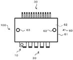
- FIG. 2 is a plan view of the semiconductor device according to the first embodiment of the present invention.
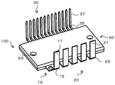
- FIG. 3 is a perspective view of the semiconductor device according to the first embodiment of the present invention.
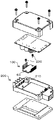
- FIG. 4 is an assembly diagram when the semiconductor device according to the first embodiment of the present invention is mounted on a housing.
- FIG. 5 (a) is a plan view after the semiconductor device according to the first embodiment of the present invention is mounted on the housing
- FIG. 5 (b) is a straight line BB in FIG. 5 (a). It is sectional drawing at the time of cut
- FIG. 5 (a) is a plan view of the semiconductor device according to the first embodiment of the present invention when not resin-sealed.
- FIG. 2 is a plan view of the semiconductor device according to the first embodiment of the present invention.
- FIG. 3 is a perspective view of the semiconductor device according to the first embodiment of the
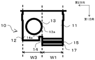
- FIG. 6 is an enlarged plan view of the vicinity of the positioning hole of the semiconductor device according to the example of the first embodiment of the present invention.
- FIG. 7 is an enlarged plan view of the vicinity of the positioning hole of the semiconductor device according to another example of the first embodiment of the present invention.
- FIG. 8 is an enlarged plan view of the second lead according to the first embodiment of the present invention.
- FIG. 9 is a plan view before the first lead, the second lead, and the third lead are formed by cutting in the first embodiment of the present invention.
- FIG. 10 is a plan view of a semiconductor device according to the second embodiment of the present invention.
- the semiconductor device 100 of the present embodiment includes a main body 50 and a plurality of semiconductor elements 51 mounted on the main body 50 via a plurality of conductive layers 52.
- the semiconductor device 100 covers the main body 50 and the semiconductor element 51 with a sealing resin 62 and is electrically connected to the sealing element 60 (see FIG. 2) fixed to the external member and the semiconductor element 51, and sealed. It also has a first lead 10 (see FIG. 1) that protrudes in the first direction outward from the stop 60.
- the semiconductor element 51 and the first lead 10, the second lead 20 and the third lead 30 described later are electrically connected by being connected by the conductive layer 52, the wire 53, and the like.
- the main body 50 of the present embodiment has a plate shape, and a plurality of semiconductor elements 51 are placed on the main body 50 having the plate shape.
- “first direction” means “downward direction” in FIG.
- the sealing part 60 includes a frame body 61 and a sealing resin 62 filled in the frame body 61.
- the frame body 61 is provided with a through hole 63 into which a fixing member 230 such as a screw (see FIG. 4) is inserted in order to fix the frame body 61 to an external member.
- a fixing member 230 such as a screw (see FIG. 4) is inserted in order to fix the frame body 61 to an external member.
- a housing 200 (see FIG. 4) mounted on a vehicle can be given.
- the case 200 is described as an external member, but the present invention is not limited to this.
- the first lead 10 of the present embodiment has a plate shape. As shown in FIGS. 6 and 7, the first lead 10 protrudes from the first base end portion 11 in a second direction different from the first direction, and a first base end portion 11 provided along the first direction. And a protrusion 12 having a positioning hole 13 into which a positioning projection 210 (see FIGS. 4 and 5) is inserted, and a first base end 11 provided with a bent portion 15 in a first direction.
- the first tip 17 extends in a direction different from the second direction and is electrically connected to an external circuit.
- “second direction” means “left direction” in FIG.
- the positioning protrusions 210 shown in FIGS. 4 and 5 are made of, for example, a resin material.
- the positioning protrusion 210 may be slightly smaller than the positioning hole 13, and the semiconductor device 100 may be rotatable with the positioning protrusion 210 inserted into the positioning hole 13.
- the positioning protrusion 210 has a tapered shape, and when the positioning protrusion 210 is inserted into the positioning hole 13, the inner peripheral surface of the positioning hole 13 and the outer peripheral surface of the positioning protrusion 210 may come into contact with each other. In such a state, the semiconductor device 100 may be rotatable.
- a slit 14 is formed in the protruding portion 12 of the first lead 10.
- the first base end of the positioning hole 13 on a straight line extending in the first direction from the slit side end portion 14a on the bent portion side of the slit 14 (see FIG. 7) or on the opposite side of the bent portion 15 from the straight line.
- the positioning hole side end 13a on the part 11 side may be located.
- the positioning hole side end portion 13a on the first base end portion 11 side is positioned on a straight line extending in the first direction from the slit side end portion 14a on the bending portion side.
- a straight line extending along the first direction having a thickness of 1/50 of the width of the first lead 10 (the length in the horizontal direction in FIGS. 6 and 7) is positioned at the end portion 14a. Moreover, it means that the positioning hole side end portion 13a on the first base end portion 11 side is located on the straight line.
- a straight line extending along the first direction has the same meaning as a straight line extending along a “third direction” to be described later, in this embodiment, “a straight line extending along the first direction”. Is used.
- the slit 14 may be provided adjacent to the bent portion 15 in the second direction. Further, the length of the slit 14 can be set to 1/25 to 1/5 of the length of the first base end portion 11 protruding outward from the sealing portion 60, for example. By lengthening the length of the slit 14, the effect which suppresses that the positioning hole 13 mentioned later deform
- the projection protrudes outward from the sealing portion 60, and is aligned with the first lead 10 along one side surface (lower side surface in FIG. 1) of the sealing portion 60.
- a second lead 20 to be disposed is provided.
- the first lead 10 is positioned on the side in the width direction end portion on one side with respect to the second lead 20. More specifically, a plurality (four) of second leads 20 are provided in the present embodiment.
- the first lead 10 is provided on the left side in FIG. 1, which is one of the end portions in the width direction from the second lead 20.
- the second lead 20 of the present embodiment has a plate shape. As shown in FIG. 8, each of the second leads 20 is provided with a second base end portion 21 provided along the first direction and a bent portion 25 at the second base end portion 21, and the first direction And a second tip 27 that extends in a direction different from the second direction and is electrically connected to an external circuit. In the present embodiment, as an example, as shown in FIG. 3, the second tip portion 27 extends in a direction perpendicular to the first direction and the second direction, and extends in parallel with the first tip portion 17.
- the protruding portion 12 may protrude from the first base end portion 11 in the direction in which the second lead 20 does not exist. In the aspect shown in FIG. 1, the protruding portion 12 protrudes from the first base end portion 11 in the left direction of FIG. 1.
- the width W1 (see FIGS. 6 and 7) of the first base end portion 11 of the first lead 10 may be the same as the width W2 (see FIG. 8) of the second base end portion 21.
- the width W ⁇ b> 1 of the first base end portion 11 may be larger or smaller than the width W ⁇ b> 2 of the second base end portion 21.
- the width W 1 of the first base end portion 11 is the same as the width of the bent portion 15 of the first lead 10
- the width W 2 of the second base end portion 21 is the bent portion of the second lead 20. It is the same size as the width of the portion 25.
- “the same size” means that it is within a range of ⁇ 5% with respect to the overall size. That is, the width W1 of the first base end portion 11 is the same as the width W2 of the second base end portion 21 because W1 is within the range of 0.95 ⁇ W2 to 1.05 ⁇ W2. It means that there is.
- the width W3 (see FIGS. 6 and 7) of the protruding portion 12 may be smaller or larger than the width W1 of the first base end portion 11. Further, the width W3 of the protruding portion 12 may be the same size as the width W1 of the first base end portion 11. Note that the width W ⁇ b> 3 of the protruding portion 12 may be determined based on the size of the positioning hole 13. When the size of the positioning hole 13 is small, the width W3 of the protrusion 12 can be reduced, and the size of the first lead 10 in the width direction can be reduced.
- a third lead 30 that protrudes outward from the sealing portion 60 and is disposed along the other side surface of the sealing portion 60 may be provided.
- the sealing part 60 of the present embodiment has a substantially rectangular shape.
- the “other side surface” in the present embodiment means a side surface opposite to “one side surface”, and means the upper side surface in FIG.
- a plurality of third leads 30 may be provided.
- Each of the third leads 30 includes a third base end portion 31 provided along a third direction (upward direction in FIG. 1) opposite to the first direction, and a bent portion 35 at the third base end portion 31. And a third tip portion 37 that extends in a direction different from the third direction and the second direction, and is electrically connected to an external circuit. As shown in FIG. 3, in the present embodiment, the third tip portion 37 extends in a direction orthogonal to the third direction and the second direction, and extends in parallel with the first tip portion 17 and the second tip portion 27. ing. In FIG. 1, the direction opposite to the second direction is shown as the fourth direction.
- the width of the third base end portion 31 is narrower than the width W2 of the second base end portion 21.
- the number of third leads 30 is larger than the total number of first leads 10 and second leads 20.
- the width of the third base end portion 31 may be larger than the width W2 of the second base end portion 21.
- the number of third leads 30 may be less than the total number of first leads 10 and second leads 20.
- FIG. 9 shows a plan view of members before being cut to form the first lead 10, the second lead 20, and the third lead 30.
- the flat lead frame 110 is formed with the flat pre first lead 10a, the pre second lead 20a, and the pre third lead 30a.
- the positioning hole 13 is on the first direction side (the lower side in FIG. 9) from the tie bar 80 and in the third direction side (see FIG. 9) from the portion 17a where the bent portion 15 is to be formed. 9 above).
- the distal end side may be bent at approximately 90 degrees while the base end portions 11, 21, and 31 are held by a holding portion (not shown).
- the first lead 10 electrically connected to the semiconductor element 51 and the external circuit is provided. For this reason, there is no need to separately provide a positioning terminal that is not electrically connected to the semiconductor element 51 as in JP-A-2015-120367. Therefore, the outer size can be made comparable to the conventional size (the outer size can be reduced as compared with the semiconductor device disclosed in Japanese Patent Application Laid-Open No. 2015-120367).
- a slit 14 is provided in the protruding portion 12, and the positioning hole 13 is located on the opposite side of the bent portion 15 from the straight side extending in the first direction from the slit-side end portion 14 a on the bent portion side of the slit 14.
- the center portion Since the center portion is located, distortion of the shape of the positioning hole 13 formed in the protruding portion 12 when the bent portion 15 is formed by bending can be prevented. For this reason, in the semiconductor device 100 of the present embodiment, the deformation of the positioning hole 13 due to the bending process when forming the bent portion 15 is suppressed. As a result, positioning using the positioning hole 13 can be performed with high accuracy. It should be noted that the ability to perform positioning with high accuracy as in the present embodiment contributes to rapid manufacturing and assembly, and is strongly desired particularly in the case of mass production such as a vehicle.
- the positioning hole side end portion 13a on the first base end portion 11 side is positioned on the “straight line” extending along the first direction from the slit side end portion 14a on the bent portion side.
- this mode it is beneficial in that the size of the protruding portion 12 in the width direction (second direction) can be reduced as much as possible while more reliably preventing the shape of the positioning hole 13 from being distorted. is there.
- the bent portion 15 is formed by bending. It is possible to efficiently block the applied stress by the adjacent slit 14.
- the size of the protruding portion 12 in the width direction (second direction) can be made as small as possible.
- the first lead 10 is located on the width direction end portion side (the left side in FIGS. 1 and 2) on one side surface than the second lead 20. Is adopted, the first lead 10 and the second lead (s) 20 can be arranged evenly. Further, since there is a vacant space at the end in the width direction, the first lead 10 is disposed at the end in the width direction (the left end in FIGS. 1 and 2) to reduce the size of the semiconductor device 100. From the point of view, it is beneficial.
- the protruding portion 12 in the case where the protruding portion 12 is protruded from the first base end portion 11 in the direction in which the second lead 20 does not exist, the protruding portion 12 is Since it is located at the end portion in the width direction, the first base end portion 11 of the first lead 10 and the second base end portion 21 of the second lead (s) 20 can be evenly arranged.
- the first lead 10 and the second lead 20 are used. It can be expected that the resistance at is approximately the same value. This is because even if a voltage is applied, it is assumed that current does not flow so much through the protruding portion 12 in which the positioning hole 13 is formed.
- the semiconductor device 100 is designed and manufactured with the first lead 10 having substantially the same performance as the second lead 20. It is beneficial in that it can.
- the sealing resin 62 for forming the sealing portion 60 is formed.
- the resin can be prevented from leaking through the positioning hole 13. Since the positioning hole 13 is positioned on the third direction side (the upper side in FIG. 9) from the portion 17a where the bent portion 17 is to be formed, the positioning hole 13 is distorted when the bent portion 17 is formed. Can be prevented.
- first leads 10 are provided.
- One side of the first lead 10 is located on one side of the side surface of the second lead 20 in the width direction (left side in FIG. 10), and the other side of the first lead 10 is the side of the side surface of the second lead 20 in the width direction. It is located on the end side (right side in FIG. 10).
- Each projecting portion 12 projects from the first base end portion 11 in a direction in which the second lead 20 does not exist. That is, in the 1st lead 10 located in the width direction one end part side, the protrusion part 12 protrudes from the 1st base end part 11 to the left side of FIG. 10, and in the 1st lead 10 located in the width direction other end part side, it protrudes. The portion 12 protrudes from the first base end portion 11 to the right side of FIG.
- the present embodiment can achieve the same effects as those of the first embodiment. Further, according to the present embodiment, since the two first leads 10 are provided, positioning can be performed at two points when the semiconductor device 100 is attached to the housing 200. For this reason, the semiconductor device 100 can be positioned without being rotated only by inserting the positioning protrusion 210 into the positioning hole 13. Therefore, a higher positioning effect can be expected more quickly. As described above, particularly in the case of mass production such as a vehicle, rapid manufacturing and assembly are strongly demanded, so that a higher positioning effect can be expected more quickly as in this embodiment. Will be very useful.
Landscapes
- Structures Or Materials For Encapsulating Or Coating Semiconductor Devices Or Solid State Devices (AREA)
- Lead Frames For Integrated Circuits (AREA)
Abstract
Description
なお、リードフレームを構成する厚板金属板に備えられたネジ止め穴の両側もしくは周辺にスリットを配置することは知られているが(特開2002-305280)、この特開2002-305280で用いられているスリットは、スリットに囲まれた範囲を押し出す加工を施すために用いられているに過ぎない。
本体部と、
前記本体部に実装された半導体素子と、
前記本体部及び前記半導体素子を封止樹脂で覆い、外部部材に対して固定される封止部と、
前記半導体素子と電気的に接続され、前記封止部から外方である第1方向に突出した第1リードと、
を備え、
前記第1リードが、前記第1方向に沿って設けられた第1基端部と、前記第1方向と異なる第2方向に前記第1基端部から突出するとともに位置決め突起が挿入されるための位置決め穴が形成された突出部と、前記第1基端部に屈曲部を介して設けられ、前記第1方向及び前記第2方向と異なる方向に延び、外部回路と電気的に接続するための第1先端部とを有し、
前記突出部にはスリットが形成されており、
前記スリットの屈曲部側のスリット側端部から前記第1方向に沿って延びた直線よりも屈曲部と反対側に、前記位置決め穴の中心部が位置している。
前記スリットの屈曲部側のスリット側端部から前記第1方向に沿って延びた直線上に又は当該直線よりも屈曲部と反対側に、前記位置決め穴の第1基端部側の位置決め穴側端部が位置していてもよい。
前記スリットは、前記第2方向において前記屈曲部に隣接して設けられてもよい。
前記封止部から外方に突出し、前記封止部の一側面に沿って前記第1リードと並んで配置される第2リードをさらに備え、
前記第1リードは、前記第2リードよりも前記一側面の幅方向端部側に位置していてもよい。
前記突出部は、前記第1基端部から前記第2リードが存在しない方向に突出してもよい。
前記封止部から外方に突出し、前記封止部の一側面に沿って前記第1リードと並んで配置される第2リードをさらに備え、
前記第1リードの前記第1基端部の幅は、前記第2リードの基端部の幅と同じ大きさになっていてもよい。
前記封止部から外方に突出し、前記封止部の一側面に沿って前記第1リードと並んで配置される第2リードをさらに備え、
前記第1リードは2つ設けられており、
前記第1リードの一方は前記第2リードの前記一側面の幅方向一端部側に位置し、
前記第1リードの他方は前記第2リードの前記一側面の幅方向他端部側に位置し、
各突出部は、前記第1基端部から前記第2リードが存在しない方向に突出してもよい。
《構成》
図1に示すように、本実施の形態の半導体装置100は、本体部50と、本体部50に複数の導電層52を介して実装された複数の半導体素子51と、を有している。半導体装置100は、本体部50及び半導体素子51を封止樹脂62で覆い、外部部材に対して固定される封止部60(図2参照)と、半導体素子51と電気的に接続され、封止部60から外方である第1方向に突出した第1リード10(図1参照)も有している。なお、半導体素子51と、第1リード10、後述する第2リード20及び第3リード30とは、導電層52、ワイヤ53等によって接続されることで、電気的に接続される。本実施の形態の本体部50は板形状となっており、板形状になった本体部50上に複数の半導体素子51が載置されている。本実施の形態において「第1方向」は図1の「下方向」を意味する。
次に、上述した構成からなる本実施の形態による作用・効果であって、まだ述べていない作用・効果について説明する。
次に、本発明の第2の実施の形態について説明する。
11 第1基端部
12 突出部
13 位置決め穴
13a 位置決め穴側端部
14 スリット
14a 屈曲部側のスリット側端部
15 屈曲部
17 第1先端部
20 第2リード
50 本体部
51 半導体素子
60 封止部
62 封止樹脂
63 貫通穴
200 筐体(外部部材)
210 位置決め突起
W1 第1基端部の幅
W2 第2基端部の幅
Claims (7)
- 本体部と、
前記本体部に実装された半導体素子と、
前記本体部及び前記半導体素子を封止樹脂で覆い、外部部材に対して固定される封止部と、
前記半導体素子と電気的に接続され、前記封止部から外方である第1方向に突出した第1リードと、
を備え、
前記第1リードは、前記第1方向に沿って設けられた第1基端部と、前記第1方向と異なる第2方向に前記第1基端部から突出するとともに位置決め突起が挿入されるための位置決め穴が形成された突出部と、前記第1基端部に屈曲部を介して設けられ、前記第1方向及び前記第2方向と異なる方向に延び、外部回路と電気的に接続するための第1先端部とを有し、
前記突出部にはスリットが形成されており、
前記スリットの屈曲部側のスリット側端部から前記第1方向に沿って延びた直線よりも屈曲部と反対側に、前記位置決め穴の中心部が位置していることを特徴とする半導体装置。 - 前記スリットの屈曲部側のスリット側端部から前記第1方向に沿って延びた直線上に又は当該直線よりも屈曲部と反対側に、前記位置決め穴の第1基端部側の位置決め穴側端部が位置していることを特徴とする請求項1に記載の半導体装置。
- 前記スリットは、前記第2方向において前記屈曲部に隣接して設けられていることを特徴とする請求項1又は2のいずれかに記載の半導体装置。
- 前記封止部から外方に突出し、前記封止部の一側面に沿って前記第1リードと並んで配置される第2リードをさらに備え、
前記第1リードは、前記第2リードよりも前記一側面の幅方向端部側に位置していることを特徴とする請求項1乃至3のいずれかに記載の半導体装置。 - 前記突出部は、前記第1基端部から前記第2リードが存在しない方向に突出することを特徴とする請求項4に記載の半導体装置。
- 前記封止部から外方に突出し、前記封止部の一側面に沿って前記第1リードと並んで配置される第2リードをさらに備え、
前記第1リードの前記第1基端部の幅は、前記第2リードの基端部の幅と同じ大きさになっていることを特徴とする請求項1乃至5のいずれか1項に記載の半導体装置。 - 前記封止部から外方に突出し、前記封止部の一側面に沿って前記第1リードと並んで配置される第2リードをさらに備え、
前記第1リードは2つ設けられており、
前記第1リードの一方は前記第2リードの前記一側面の幅方向一端部側に位置し、
前記第1リードの他方は前記第2リードの前記一側面の幅方向他端部側に位置し、
各突出部は、前記第1基端部から前記第2リードが存在しない方向に突出することを特徴とする請求項1乃至6のいずれか1項に記載の半導体装置。
Priority Applications (4)
| Application Number | Priority Date | Filing Date | Title |
|---|---|---|---|
| US15/544,235 US10553523B2 (en) | 2015-11-20 | 2015-11-20 | Semiconductor device |
| CN201580077552.5A CN107431055B (zh) | 2015-11-20 | 2015-11-20 | 半导体装置 |
| PCT/JP2015/082712 WO2017085866A1 (ja) | 2015-11-20 | 2015-11-20 | 半導体装置 |
| JP2016571432A JP6255518B2 (ja) | 2015-11-20 | 2015-11-20 | 半導体装置 |
Applications Claiming Priority (1)
| Application Number | Priority Date | Filing Date | Title |
|---|---|---|---|
| PCT/JP2015/082712 WO2017085866A1 (ja) | 2015-11-20 | 2015-11-20 | 半導体装置 |
Publications (1)
| Publication Number | Publication Date |
|---|---|
| WO2017085866A1 true WO2017085866A1 (ja) | 2017-05-26 |
Family
ID=58718716
Family Applications (1)
| Application Number | Title | Priority Date | Filing Date |
|---|---|---|---|
| PCT/JP2015/082712 Ceased WO2017085866A1 (ja) | 2015-11-20 | 2015-11-20 | 半導体装置 |
Country Status (4)
| Country | Link |
|---|---|
| US (1) | US10553523B2 (ja) |
| JP (1) | JP6255518B2 (ja) |
| CN (1) | CN107431055B (ja) |
| WO (1) | WO2017085866A1 (ja) |
Families Citing this family (2)
| Publication number | Priority date | Publication date | Assignee | Title |
|---|---|---|---|---|
| JP6929788B2 (ja) * | 2015-12-04 | 2021-09-01 | ローム株式会社 | パワーモジュール装置、および電気自動車またはハイブリッドカー |
| EP3961692A4 (en) * | 2019-04-25 | 2023-05-24 | Kyocera Corporation | CIRCUIT BOARD, ENCAPSULATION OF AN ELECTRONIC ELEMENT PACKAGE AND ELECTRONIC DEVICE |
Citations (6)
| Publication number | Priority date | Publication date | Assignee | Title |
|---|---|---|---|---|
| JPS63105355U (ja) * | 1986-12-25 | 1988-07-08 | ||
| JPH0220318U (ja) * | 1988-07-26 | 1990-02-09 | ||
| JPH04129259A (ja) * | 1990-09-19 | 1992-04-30 | Matsushita Electric Ind Co Ltd | 電子部品 |
| US5521427A (en) * | 1992-12-18 | 1996-05-28 | Lsi Logic Corporation | Printed wiring board mounted semiconductor device having leadframe with alignment feature |
| JP2002118341A (ja) * | 2000-10-05 | 2002-04-19 | Fujitsu Denso Ltd | 電子部品、電子部品の取付構造、一次接続用端子、電子部品の取付方法 |
| JP2003197469A (ja) * | 2001-12-28 | 2003-07-11 | Elna Co Ltd | チップ型電子部品 |
Family Cites Families (9)
| Publication number | Priority date | Publication date | Assignee | Title |
|---|---|---|---|---|
| US2020318A (en) * | 1934-03-06 | 1935-11-12 | Bell Telephone Labor Inc | System including repeater |
| JPS57106061A (en) * | 1980-12-24 | 1982-07-01 | Toshiba Corp | Semiconductor integrated circuit device |
| US5053357A (en) * | 1989-12-27 | 1991-10-01 | Motorola, Inc. | Method of aligning and mounting an electronic device on a printed circuit board using a flexible substrate having fixed lead arrays thereon |
| JP2002305280A (ja) | 2001-04-06 | 2002-10-18 | Matsushita Electric Ind Co Ltd | 半導体装置 |
| JP2004023017A (ja) * | 2002-06-20 | 2004-01-22 | Sony Corp | 中空パッケージ及びラインセンサ |
| JP5647912B2 (ja) * | 2011-02-02 | 2015-01-07 | 新電元工業株式会社 | 電子回路装置及びその製造方法 |
| CN103617965B (zh) * | 2013-11-20 | 2019-02-22 | 常州唐龙电子有限公司 | 一种外型具有引线的扁平集成电路封装结构 |
| JP2015120367A (ja) | 2013-12-20 | 2015-07-02 | 日本精工株式会社 | 電子制御ユニット、電動パワーステアリング装置及び車両 |
| US10217727B2 (en) * | 2014-08-25 | 2019-02-26 | Renesas Electronics Corporation | Semiconductor device and electronic apparatus including a first semiconductor chip including an insulated gate bipolar transistor and a second semiconductor chip including a diode |
-
2015
- 2015-11-20 US US15/544,235 patent/US10553523B2/en active Active
- 2015-11-20 WO PCT/JP2015/082712 patent/WO2017085866A1/ja not_active Ceased
- 2015-11-20 CN CN201580077552.5A patent/CN107431055B/zh active Active
- 2015-11-20 JP JP2016571432A patent/JP6255518B2/ja active Active
Patent Citations (6)
| Publication number | Priority date | Publication date | Assignee | Title |
|---|---|---|---|---|
| JPS63105355U (ja) * | 1986-12-25 | 1988-07-08 | ||
| JPH0220318U (ja) * | 1988-07-26 | 1990-02-09 | ||
| JPH04129259A (ja) * | 1990-09-19 | 1992-04-30 | Matsushita Electric Ind Co Ltd | 電子部品 |
| US5521427A (en) * | 1992-12-18 | 1996-05-28 | Lsi Logic Corporation | Printed wiring board mounted semiconductor device having leadframe with alignment feature |
| JP2002118341A (ja) * | 2000-10-05 | 2002-04-19 | Fujitsu Denso Ltd | 電子部品、電子部品の取付構造、一次接続用端子、電子部品の取付方法 |
| JP2003197469A (ja) * | 2001-12-28 | 2003-07-11 | Elna Co Ltd | チップ型電子部品 |
Also Published As
| Publication number | Publication date |
|---|---|
| US20180269132A1 (en) | 2018-09-20 |
| CN107431055B (zh) | 2019-07-26 |
| JPWO2017085866A1 (ja) | 2017-11-16 |
| JP6255518B2 (ja) | 2017-12-27 |
| CN107431055A (zh) | 2017-12-01 |
| US10553523B2 (en) | 2020-02-04 |
Similar Documents
| Publication | Publication Date | Title |
|---|---|---|
| JP5341114B2 (ja) | ワイヤ素子とワイヤ素子を固定する少なくとも1つのバンプを備えた溝を有するマイクロエレクトロニックチップのアセンブリ | |
| JP6426945B2 (ja) | 蓄電装置 | |
| CN111587486B (zh) | 半导体装置以及半导体装置的制造方法 | |
| CN107615438A (zh) | 熔丝制造方法及熔丝 | |
| US11804352B2 (en) | Fuse | |
| JP6255518B2 (ja) | 半導体装置 | |
| JP6638262B2 (ja) | 回路構成体 | |
| CN113257767A (zh) | 传递模塑型功率模块、引线框架及传递模塑型功率模块的制造方法 | |
| JP2019047061A (ja) | 半導体装置およびその製造方法 | |
| JP6080305B2 (ja) | 半導体装置の製造方法、半導体装置及びリードフレーム | |
| WO2016167095A1 (ja) | プレスフィット端子及び基板用コネクタ | |
| JP2007150139A (ja) | インダクタ | |
| JP4454357B2 (ja) | 樹脂封止型半導体装置及びその製造方法 | |
| JP2012238792A (ja) | 板状抵抗体を有する抵抗器及びその製造方法 | |
| CN109087903A (zh) | 电子装置、用于电子装置的引线框架以及制造电子装置和引线框架的方法 | |
| JP6128687B2 (ja) | 半導体装置の製造方法、半導体装置及びリードフレーム | |
| JP6346717B1 (ja) | 電子装置及び接続体 | |
| JP6472931B1 (ja) | 電子モジュール | |
| JP6325757B1 (ja) | 電子装置 | |
| KR200370034Y1 (ko) | 블로워모터용 레지스터 | |
| JP6186204B2 (ja) | 半導体装置及びリードフレーム | |
| US6432747B1 (en) | Repair method for broken or missing microcircuit package terminal lead | |
| US20210020382A1 (en) | Electrolytic Capacitor with Improved Connection Part | |
| JP2015005687A (ja) | 樹脂パッケージとこの樹脂パッケージを用いた電子機器 | |
| US20200219797A1 (en) | Electronic device, connection body, and manufacturing method for electronic device |
Legal Events
| Date | Code | Title | Description |
|---|---|---|---|
| ENP | Entry into the national phase |
Ref document number: 2016571432 Country of ref document: JP Kind code of ref document: A |
|
| 121 | Ep: the epo has been informed by wipo that ep was designated in this application |
Ref document number: 15908806 Country of ref document: EP Kind code of ref document: A1 |
|
| WWE | Wipo information: entry into national phase |
Ref document number: 15544235 Country of ref document: US |
|
| NENP | Non-entry into the national phase |
Ref country code: DE |
|
| 122 | Ep: pct application non-entry in european phase |
Ref document number: 15908806 Country of ref document: EP Kind code of ref document: A1 |