WO2017073409A1 - 有機el素子の製造方法 - Google Patents
有機el素子の製造方法 Download PDFInfo
- Publication number
- WO2017073409A1 WO2017073409A1 PCT/JP2016/080865 JP2016080865W WO2017073409A1 WO 2017073409 A1 WO2017073409 A1 WO 2017073409A1 JP 2016080865 W JP2016080865 W JP 2016080865W WO 2017073409 A1 WO2017073409 A1 WO 2017073409A1
- Authority
- WO
- WIPO (PCT)
- Prior art keywords
- organic
- layer
- glass transition
- anode
- transition temperature
- Prior art date
- Legal status (The legal status is an assumption and is not a legal conclusion. Google has not performed a legal analysis and makes no representation as to the accuracy of the status listed.)
- Ceased
Links
Images




Classifications
-
- H—ELECTRICITY
- H05—ELECTRIC TECHNIQUES NOT OTHERWISE PROVIDED FOR
- H05B—ELECTRIC HEATING; ELECTRIC LIGHT SOURCES NOT OTHERWISE PROVIDED FOR; CIRCUIT ARRANGEMENTS FOR ELECTRIC LIGHT SOURCES, IN GENERAL
- H05B33/00—Electroluminescent light sources
- H05B33/10—Apparatus or processes specially adapted to the manufacture of electroluminescent light sources
-
- H—ELECTRICITY
- H10—SEMICONDUCTOR DEVICES; ELECTRIC SOLID-STATE DEVICES NOT OTHERWISE PROVIDED FOR
- H10K—ORGANIC ELECTRIC SOLID-STATE DEVICES
- H10K50/00—Organic light-emitting devices
- H10K50/10—OLEDs or polymer light-emitting diodes [PLED]
- H10K50/11—OLEDs or polymer light-emitting diodes [PLED] characterised by the electroluminescent [EL] layers
Definitions
- the present invention relates to a method for producing an organic EL element.
- Patent Document 1 As a method for producing an organic electroluminescence (organic EL) element, a method described in Patent Document 1 is known.
- a bonding method is adopted for the sequential film forming method described in Patent Document 1 from the viewpoint of productivity.
- at least one first organic layer containing an organic compound having a reactive substituent is formed on one of the anode and the cathode, and at least one second organic layer is formed on the other electrode.
- the first organic layer and the second organic layer are bonded to face each other to manufacture an organic EL element.
- the first and second organic layers are heated and bonded at a temperature equal to or lower than the glass transition temperature of the first and second organic layers.
- heating conditions at this time include heating at 100 ° C. for 1 hour.
- the form which irradiates the activation light which activates the reactive substituent which a 1st organic layer has is also disclosed.
- an object of the present invention is to provide a method for producing an organic EL element which can improve productivity and has high electron transportability at the interface in the bonding method.
- the organic EL device manufacturing method includes an anode and a first organic layer on a first substrate, and the first organic layer is formed on the first substrate.
- a first structure located on the outermost side is prepared, and a cathode and a second organic layer are provided on the second substrate, and the second organic layer is formed on the second substrate.
- a step of preparing the second structure located on the outermost side, and the first organic layer of the first structure and the second organic layer of the second structure facing each other And bonding the first and second structures to each other.
- the first and second structures are bonded to each other by heating the first and second structures at a temperature higher than a predetermined glass transition temperature by 10 ° C. or more.
- the predetermined glass transition temperature is higher among the glass transition temperature of the first organic layer of the first structure and the glass transition temperature of the second organic layer of the second structure. There is no glass transition temperature.
- the heating temperature at the time of laminating the first and second structures satisfies the above-described conditions, for example, the heating time can be shortened compared to the case of heating at the predetermined glass transition temperature or lower, and the manufactured organic In the EL element, the adhesion at the interface between the first and second structures is improved and carrier movement is not easily inhibited. As a result, the productivity of the organic EL element can be improved, and the electron transport property at the interface can be improved in the bonding method.
- the organic layer having the predetermined glass transition temperature may include an organic substance having the predetermined glass transition temperature and having a molecular weight of 1000 or more. Since an organic substance having a molecular weight of 1000 or more is less likely to be crystallized, a higher temperature can be realized under the above heating conditions. As a result, productivity can be further improved.
- productivity can be improved and a method for producing an organic EL element having a high electron transport property at the interface in the bonding method can be provided.
- FIG. 1 is a schematic diagram illustrating a schematic configuration of an organic EL element according to an embodiment.
- FIG. 2 is a diagram for explaining a method for manufacturing an organic EL element according to an embodiment.
- FIG. 2A shows an example of a first structure
- FIG. FIG. 2C illustrates an example of the second structure
- FIG. 2C illustrates a bonding process of the first structure and the second structure illustrated in FIGS. ing.
- FIG. 3 is a schematic diagram showing a schematic configuration of organic EL elements used in Examples 1 to 3 and Reference Examples 1 to 3.
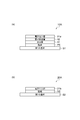
- FIG. 4 is a schematic diagram showing a schematic configuration of first and second structures prepared for producing organic EL elements for Example 1, Example 2, Reference Example 1 and Reference Example 2.
- FIG. 1 is a schematic diagram illustrating a schematic configuration of an organic EL element according to an embodiment.
- FIG. 2 is a diagram for explaining a method for manufacturing an organic EL element according to an embodiment.
- FIG. 2A shows an example of a first structure
- FIG. 4A shows a schematic configuration of a first structure prepared for manufacturing organic EL elements for Example 1, Example 2, Reference Example 1 and Reference Example 2.
- FIG. 4B shows a schematic configuration of the second structure prepared for manufacturing organic EL elements for Example 1, Example 2, Reference Example 1, and Reference Example 2.
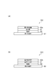
- FIG. 5 is a schematic diagram showing a schematic configuration of the first and second structures prepared for manufacturing the organic EL element for Example 3, and FIG. The schematic structure of the 1st structure prepared in order to manufacture an organic EL element is shown, (b) of FIG. 5 shows the 2nd structure prepared in order to manufacture the organic EL element for Example 3.
- FIG. The schematic structure of the body is shown.
- FIG. 6 is a schematic diagram showing a schematic configuration of the first and second structures prepared for manufacturing the organic EL element for Reference Example 3, and FIG.
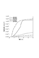
- FIG. 7 is a drawing showing the results of Example 1, Example 2, Reference Example 1 and Reference Example 2.
- FIG. 8 is a drawing showing the results of Example 1, Example 3, and Reference Example 3.
- the organic EL element 1 includes first and second base materials S1 and S2, an anode PE, a cathode NE, and a plurality of organic layers OL. Prepare. In the form shown in FIG. 1, five organic layers OL are included between the anode PE and the cathode NE. However, as will be described later, the number of organic layers OL is not limited to five.
- the organic EL element 1 can take a form in which light is emitted from the anode PE and a form in which light is emitted from the cathode NE side. Hereinafter, a form in which light is emitted from the anode PE will be described unless otherwise specified.
- the first substrate S1 is a support that supports the anode PE and at least one organic layer OL.
- the first base material S1 has a light-transmitting property with respect to visible light (light having a wavelength of 400 nm to 800 nm).
- the first base material S1 is, for example, a plastic film including a glass substrate or a plastic material.
- plastic materials include polyethersulfone (PES); polyester resins such as polyethylene terephthalate (PET) and polyethylene naphthalate (PEN); polyolefin resins such as polyethylene (PE), polypropylene (PP) and cyclic polyolefin; polyamide resins; Polycarbonate resin; polystyrene resin; polyvinyl alcohol resin; saponified ethylene-vinyl acetate copolymer; polyacrylonitrile resin; acetal resin; polyimide resin;
- polyester resin and polyolefin resin are preferable, and PET and PEN are particularly preferable because of high heat resistance, low linear expansion coefficient and low manufacturing cost.
- One of these resins may be used alone, or two or more thereof may be used in combination.
- a barrier film may be formed on the surface of the first base material S1.
- the barrier film can be, for example, a film made of silicon, oxygen, and carbon, or a film made of silicon, oxygen, carbon, and nitrogen.
- examples of the material of the barrier film are silicon oxide, silicon nitride, silicon oxynitride, and the like.
- An example of the thickness of the barrier film is 100 nm or more and 10 ⁇ m or less.
- a driving circuit for example, a circuit including a thin film transistor for driving the organic EL element 1 may be formed on the first base material S1.
- Such a drive circuit is usually made of a transparent material.
- the second base material S2 is, for example, a plastic film including a glass substrate or a plastic material.
- An example of the plastic material is the same as the example of the plastic material in the first base material S1.
- the second substrate S2 functions as a support for the cathode NE and at least one organic layer OL in the method for manufacturing an organic EL element described later.
- the anode PE can be a thin film made of metal oxide, metal sulfide, metal, and the like. Specifically, indium oxide, zinc oxide, tin oxide, indium tin oxide (Indium Tin Oxide: abbreviated as ITO), A thin film made of indium zinc oxide (Indium Zinc Oxide: abbreviation IZO), gold, platinum, silver, copper, or the like is used. In the form in which the organic EL element 1 emits light from the first base material S1 side, an electrode exhibiting optical transparency is used for the anode PE.
- the material of the cathode NE is preferably a material having a small work function, easy electron injection into a light emitting layer described later, which the organic EL element 1 has, and high electrical conductivity.
- a material having a high visible light reflectance is preferable as the material of the cathode NE in order to reflect the light emitted from the light emitting layer to the anode PE side by the cathode NE.
- an alkali metal, an alkaline earth metal, a transition metal, a group 13 metal of the periodic table, or the like can be used.
- a transparent conductive electrode made of a conductive metal oxide, a conductive organic material, or the like can be used.
- the light emitting layer is an organic layer OL having a function of emitting light of a predetermined wavelength.
- the light emitting layer is usually formed of an organic substance that mainly emits fluorescence and / or phosphorescence, or an organic substance and a dopant that assists the organic substance.
- the dopant is added, for example, to improve the light emission efficiency or to change the light emission wavelength.
- the organic substance contained in the light emitting layer may be a low molecular compound or a high molecular compound. Examples of the light emitting material constituting the light emitting layer include known dye materials, metal complex materials, polymer materials, and dopant materials.
- Examples of the organic layer OL provided between the anode PE and the light emitting layer include a hole injection layer and a hole transport layer.
- Examples of the layer provided between the cathode NE and the light emitting layer include an electron injection layer and an electron transport layer.
- materials for the hole injection layer, the hole transport layer, the electron transport layer, and the electron injection layer known materials can be used.
- the hole injection layer is an organic layer OL having a function of improving hole injection efficiency from the anode PE to the light emitting layer.
- the hole transport layer is a layer having a function of improving hole injection from the anode PE, the hole injection layer, or the hole transport layer closer to the anode PE to the light emitting layer.
- these layers may be referred to as an electron blocking layer.
- the electron injection layer is a layer having a function of improving the efficiency of electron injection from the cathode NE to the light emitting layer.
- the electron transport layer is a layer having a function of improving electron injection from the cathode NE, the electron injection layer, or the electron transport layer closer to the cathode NE.
- a known electron transport material can be used for the electron transport layer.
- the electron injection layer and / or the electron transport layer have a function of blocking hole transport, these layers may be referred to as a hole blocking layer.
- Examples of the layer configuration of the organic EL element 1 including the various organic layers OL described above are shown below.
- (A) anode / light emitting layer / cathode (b) anode / hole injection layer / light emitting layer / cathode (c) anode / hole transport layer / light emitting layer / cathode (d) anode / hole injection layer / light emitting layer / Electron injection layer / cathode (e) anode / hole injection layer / light emitting layer / electron transport layer / cathode (f) anode / hole transport layer / light emitting layer / electron injection layer / cathode (g) anode / hole transport layer / Light emitting layer / electron transport layer / cathode (h) anode / hole injection layer / light emitting layer / electron transport layer / electron injection layer / cathode (i) anode / hole transport layer / light emitting layer
- the organic EL element 1 may have a single light emitting layer or two or more light emitting layers.
- the layer configurations of (a) to (p) above if the laminated structure disposed between the anode PE and the cathode NE is “structural unit A”, it has two light emitting layers.
- the layer structure shown to the following (q) can be mentioned, for example.
- the two (structural unit A) layer structures may be the same or different.
- the charge generation layer is a layer that generates holes and electrons by applying an electric field.
- Examples of the charge generation layer include a thin film made of vanadium oxide, ITO, molybdenum oxide, or the like.
- Examples of the configuration of the organic EL element 1 having three or more light-emitting layers include the layer configuration shown in (r) below. Can do. (R) Anode / (Structural unit B) x / (Structural unit A) / Cathode
- (Structural unit B) x represents a stacked body in which (Structural unit B) is stacked in x stages.
- a plurality of (structural units B) may have the same or different layer structure.
- the organic EL element 1 may be configured by directly laminating a plurality of light emitting layers without providing a charge generation layer.
- the method for manufacturing the organic EL element 1 first, the first structure 10 and the second structure 20 shown in FIGS. 2A and 2B are prepared (structure preparation process). Next, as shown in FIG. 2C, the organic EL element 1 is obtained by bonding the first and second structures 10 and 20 (bonding step). Therefore, the plurality of organic layers OL included in the organic EL element 1 are allocated to the first and second structures 10 and 20.
- the first structural body 10 prepared in the structural body preparation step includes the anode PE and a part of the plurality of organic layers OL included in the organic EL element 1 (four organic layers OL in FIG. 2A) in this order. It is manufactured by laminating on the first substrate S1.
- the anode PE and the organic layer OL can be formed by, for example, a vapor deposition method or a coating method.
- the coating method spin coating method, casting method, micro gravure coating method, gravure coating method, bar coating method, roll coating method, wire bar coating method, dip coating method, slit coating method, capillary coating method, spray coating method, Examples thereof include a nozzle coating method, a gravure printing method, a screen printing method, a flexographic printing method, an offset printing method, a reverse printing method, and an ink jet printing method.
- the solvent of the coating solution used in the coating method is not limited as long as it dissolves the material of the target object (anode PE and organic layer OL) to be formed by the coating method.
- the material of the target object anode PE and organic layer OL
- chloroform methylene chloride, dichloroethane, etc.
- Chlorine solvents such as tetrahydrofuran, aromatic hydrocarbon solvents such as toluene and xylene, alcohol solvents such as methanol, ethanol, cyclohexanol and ethylene glycol, ketone solvents such as acetone and methyl ethyl ketone, ethyl acetate , Ester solvents such as butyl acetate and ethyl cellosolve acetate, and water.
- ether solvents such as tetrahydrofuran
- aromatic hydrocarbon solvents such as toluene and xylene
- alcohol solvents such as methanol, ethanol, cyclohexanol and ethylene glycol
- ketone solvents such as acetone and methyl ethyl ketone, ethyl acetate
- Ester solvents such as butyl acetate and ethyl cellosolve acetate, and water.
- the second structure 20 includes the cathode NE and the remaining organic layer OL of the plurality of organic layers OL included in the organic EL element 1 (one organic layer OL in FIG. 2B) in this order. It is manufactured by forming on the material S2.
- the cathode NE and the organic layer OL can be formed by, for example, a vapor deposition method or a coating method.
- An example of the coating method and an example of the solvent are the same as in the case of the first structure 10.
- the first and second structures 10 and 20 are bonded together by a bonding method. That is, an organic layer (first organic layer) OL1 that is an organic layer OL located on the opposite side as viewed from the first base material S1 in the first structure 10 and a second in the second structure 20
- the first and second structures 10 are heated by bringing the organic layer (second organic layer) OL2 that is the organic layer OL located on the opposite side of the substrate S2 into contact with each other. , 20 are pasted together. Therefore, the surface OL1a of the organic layer OL1 and the surface OL2a of the organic layer OL2 constitute the interface between the first and second structures 10 and 20.
- the heating temperature T (° C.) and the predetermined glass transition temperature is TL (° C.)
- the heating temperature T satisfies the following formula (1). TL (° C.) + 10 ° C. ⁇ T (° C.) (1)
- the predetermined glass transition temperature TL is a glass transition temperature which is not higher among the glass transition temperatures of the organic layer OL1 and the organic layer OL2. Specifically, the predetermined glass transition temperature TL corresponds to the lower glass transition temperature when the glass transition temperatures of the organic layer OL1 and the organic layer OL2 are different, and the glass transition temperatures of the organic layer OL1 and the organic layer OL2 are the same. When the temperatures are substantially the same, it corresponds to the glass transition temperature of the organic layer OL1 or the organic layer OL2.
- the upper limit of the heating temperature T can be appropriately set within a range not departing from the gist of the present invention, and may be, for example, the lowest of the melting point or decomposition temperature of the organic layer OL1 and the melting point or decomposition temperature of the organic layer OL2.
- the glass transition temperature of the organic layer OL1 and the organic layer OL2 is the glass transition temperature of the material constituting the organic layer OL1 and the organic layer OL2.
- the organic layer OL1 and organic layer OL2 are comprised from the mixture, let those glass transition temperatures be the glass transition temperature of the organic substance most contained in the mixture.
- the organic substance most contained in the mixture means the main component in the organic layer OL1, and means, for example, a component contained in a composition ratio exceeding 50%.
- the organic substance contained most in the mixture in the organic layer OL2 means the main component in the organic layer OL2, and means, for example, a component contained in the composition ratio exceeding 50%.
- the heating method is not limited, but heating by a hot plate, heating by light, and heating by jetting a hot gas can be mentioned.
- the organic EL elements 1 are manufactured by bonding them together by a bonding method. Therefore, a short circuit between the cathode NE and the anode PE hardly occurs.
- the organic layer having a predetermined glass transition temperature TL as the glass transition temperature among the organic layers OL1 and OL2 has the predetermined glass transition temperature TL as the glass transition temperature and has a molecular weight of 1000 or more. It is preferable to contain an organic substance (when the organic substance is a polymer compound, the molecular weight is a weight average molecular weight in terms of polystyrene). In this case, since it is difficult to crystallize, it is easy to realize a heating temperature satisfying the formula (1).
- the organic substance having a predetermined glass transition temperature TL as the glass transition temperature and having a molecular weight of 1000 or more can be a main component in the organic layer when the organic layer containing the organic substance is composed of a mixture.
- the definition of the main component in this specification is as described above.
- organic EL elements were manufactured for Examples 1 to 3 and Reference Examples 1 to 3.
- the produced six organic EL elements are referred to as organic EL elements E1, E2, E3, E4, E5, and E6.
- a fluorene-aromatic copolymer (glass transition temperature 144 ° C., polystyrene-equivalent weight average molecular weight 2.3 ⁇ 10 5 ) was dissolved in a xylene solvent in the air. Using the prepared solution, a film was formed on the underlayer using the spin coating method in the air. Thereafter, heating was performed on a hot plate at 130 ° C. for 10 minutes in an inert gas atmosphere to remove the residual solvent.
- a conjugated polymer compound described in paragraph 401 of JP2012-033845A (glass transition temperature 219 ° C., polystyrene-equivalent weight average molecular weight 1.5 ⁇ 10 5 ) was dissolved in a methanol solvent in the atmosphere. Using the prepared solution, a film was formed on the underlayer in the air using a spin coating method. Thereafter, heating was performed on a hot plate at 130 ° C. for 10 minutes in an inert gas atmosphere to remove the residual solvent.
- a polymer compound described in paragraph 262 of JP-A-2008-056909 (glass transition temperature 126 ° C., polystyrene-equivalent weight average molecular weight 1.7 ⁇ 10 5 ) was dissolved in a xylene solvent in the atmosphere. Thereafter, 1,3-dimethyl-2-phenyl-2,3-dihydro-1H-benzimidazole (manufactured by Aldrich) was added to the solution prepared in an inert atmosphere as described in paragraph 262 of JP-A-2008-056909. It was dissolved so as to be 25% with respect to the mass of the polymer compound. Using the prepared solution, a film was formed on the underlayer using the spin coating method in the air. Thereafter, heating was performed on a hot plate at 130 ° C. for 10 minutes in an inert gas atmosphere to remove the residual solvent.
- a film made of PEN was used as the first base material S1, and a glass substrate was used as the second base material S2.
- a thin film made of silver (Ag) was used as the anode PE, and a two-layer structure of an aluminum (Al) thin film and a zinc oxide (ZnO) thin film was used as the cathode NE.
- the anode PE was formed by a vapor deposition method.
- an aluminum thin film and a zinc oxide thin film were formed in this order from the second substrate S2 side by a vapor deposition method and a sputtering method, respectively. As shown in FIG.
- the layer configuration between the anode PE and the cathode NE in the organic EL elements E1 to E6 was the same as the configuration (p) described above.
- the thickness and material of each layer included in the organic EL elements E1 to E6 are the same.
- the light emitting layer 11, the electron transport layer 12, and the electron injection layer 21 are stacked as the organic layer OL on the anode PE, and the cathode NE is provided on the electron injection layer 21. It was.
- the glass transition temperature of the electron transport layer 12 was 219 ° C.
- the glass transition temperature of the electron injection layer 21 was 126 ° C.
- the anode PE, the light emitting layer 11, the electron transport layer 12, and the electron injection layer 21a are sequentially formed on the first base material S1.
- the first structure 10A is prepared, and the cathode NE and the electron injection layer 21b are sequentially formed on the second base material S2 as shown in FIG.
- the structure 20A was prepared.
- the underlayer for each of the light emitting layer 11, the electron transport layer 12, and the electron injection layer 21a is the anode PE, the light emitting layer 11, and the electron transport layer 12, and the second structure 20A.
- the base layer for the electron injection layer 21b is the cathode NE.
- the outermost layer was the electron injection layer 21a in the stacked structure on the first substrate S1.
- the outermost layer in the stacked structure on the second base material S2 was the electron injection layer 21b.
- the electron injection layers 21a and 21b are layers that are bonded to become the electron injection layer 21 of the organic EL element E1 shown in FIG. That is, the thicknesses of the electron injection layers 21 a and 21 b are set so that the total thickness of the electron injection layers 21 a and 21 b is the same as the thickness of the electron injection layer 21. In FIG. 4A and FIG. 4B, the thicknesses of the electron injection layers 21a and 21b are shown thick for illustration.
- the organic EL element E1 was obtained by heating with a hot plate and bonding the electron injection layer 21a and the electron injection layer 21b.
- the hot plate was heated at 150 ° C. for 20 minutes.
- the glass transition temperature of the electron injection layers 21a and 21b is the same as the glass transition temperature of the electron injection layer 21 described above.
- Organic EL element E3 (Manufacture of organic EL element E3) Organic EL except that the heating temperature was changed to 110 ° C. when the first structure 10A and the second structure 20A shown in FIGS. 4A and 4B were bonded together. Organic EL element E3 was manufactured by the same method as element E1.
- Organic EL element E4 (Manufacture of organic EL element E4) Organic EL except that the heating temperature was changed to 130 ° C. when the first structure 10A and the second structure 20A shown in FIGS. 4A and 4B were bonded together. Organic EL element E4 was manufactured by the same method as element E1.
- the anode PE, the light emitting layer 11, and the electron transport layer 12 are sequentially formed on the first base material S1, thereby forming the first.
- the structure 10B is prepared, and as shown in FIG. 5B, the second structure 20B is formed by sequentially forming the cathode NE and the electron injection layer 21 on the second substrate S2. Got ready.
- the base layers for the light emitting layer 11 and the electron transport layer 12 are the anode PE and the light emitting layer 11, respectively, and in the preparation of the second structure 20B.
- the base layer for the electron injection layer 21 is a cathode NE.
- the outermost layer was the electron transport layer 12 in the stacked structure on the first base material S1.
- the outermost layer was the electron injection layer 21 in the stacked structure on the second base material S2. Then, after overlapping the electron transport layer 12 of the first structure 10B and the electron injection layer 21 of the second structure 20B facing each other, the first and second structures 10B and 20B are heated.
- the organic EL element E5 was obtained by heating with a plate and bonding the electron carrying layer 12 and the electron injection layer 21 together. The hot plate was heated at 150 ° C. for 20 minutes.
- the anode PE, the light emitting layer 11, and the electron transport layer 12a are sequentially formed on the first base material S1, thereby forming the first.
- the structure 10C is prepared, and the cathode NE, the electron injection layer 21 and the electron transport layer 12b are sequentially formed on the second substrate S2 as shown in FIG.
- the structure 20C was prepared.
- the base layers for the light emitting layer 11 and the electron transport layer 12a are the anode PE and the light emitting layer 11, respectively, and in the preparation of the second structure 20C, the electron injection layer 21 and the electron
- the underlayer for each of the transport layers 12 b is a cathode NE and an electron injection layer 21.
- the outermost layer was the electron transport layer 12a in the stacked structure on the first substrate S1.
- the outermost layer was the electron transport layer 12b in the stacked structure on the second substrate S2.
- the electron transport layers 12a and 12b are layers that are bonded to become the electron transport layer 12 of the organic EL element E6 shown in FIG. That is, the thicknesses of the electron transport layers 12 a and 12 b are set so that the total thickness of the electron transport layers 12 a and 12 b is the same as the thickness of the electron transport layer 12. In FIGS. 6A and 6B, the thicknesses of the electron transport layers 12a and 12b are shown to be thick for illustration.
- the organic EL element E6 was obtained by heating with a hot plate and bonding the electron transport layer 12a and the electron transport layer 12b.
- the hot plate was heated at 150 ° C. for 20 minutes.
- the glass transition temperature of the electron transport layers 12a and 12b is the same as the glass transition temperature of the electron transport layer 12 described above.
- Example 1 A voltage was applied between the anode PE and the cathode NE included in the organic EL element E1, and the electron transport property at the interface was evaluated based on the current density while changing the applied voltage.
- Example 2 A voltage is applied between the anode PE and the cathode NE of the organic EL element E2 in the same manner as in Example 1, and the electron transport property at the interface is changed based on the current density while changing the applied voltage as in Example 1. evaluated.
- Reference Example 1 A voltage is applied between the anode PE and the cathode NE of the organic EL element E3 in the same manner as in Example 1, and the electron transport property at the interface is changed based on the current density while changing the applied voltage as in Example 1. evaluated.
- Example 2 A voltage is applied between the anode PE and the cathode NE of the organic EL element E4 in the same manner as in Example 1, and the electron transport property at the interface is changed based on the current density while changing the applied voltage as in Example 1. evaluated.
- Example 3 A voltage is applied between the anode PE and the cathode NE of the organic EL element E5 in the same manner as in Example 1, and the electron transport property at the interface is changed based on the current density while changing the applied voltage as in Example 1. evaluated.
- the organic EL elements E1 and E2 manufactured at the heating temperature satisfying the formula (1) have a higher current than the organic EL elements E3 and E4 manufactured at the heating temperature not satisfying the expression (1). It can be seen that the density is realized, and the organic EL elements E1 and E2 have improved electron transport properties at the interface as compared with the organic EL elements E3 and E4.
- Example 1 The results of Example 1, Example 3 and Reference Example 3 were as shown in FIG.
- the heating temperature in the production of the organic EL element E1 satisfies the formula (1).
- the two organic layers constituting the interface between the first and second structures 10B and 20B are the electron transport layer 12 and the electron injection layer 21, and the glass transition temperature thereof is 219. And 126 ° C. Therefore, the heating temperature in the production of the organic EL element E5 also satisfied the formula (1).
- the two organic layers constituting the interface between the first and second structures 10C and 20C are the electron transport layers 12a and 12b, and the glass transition temperature thereof is 219 ° C. Met. Therefore, the heating temperature in manufacturing the organic EL element E6 did not satisfy the formula (1).
- the organic EL elements E1 and E5 manufactured at the heating temperature satisfying the formula (1) have a higher current density than the organic EL element E6 manufactured at the heating temperature not satisfying the expression (1). It can be seen that the organic EL elements E1 and E5 have improved electron injection properties than the organic EL element E6. That is, the electron transport property at the interface can be improved when the heating temperature satisfies the formula (1) without depending on the material of the organic layer that is in contact with the first and second structures. I understand.
- the heating temperature at the time of bonding the first and second structures 10 and 20 satisfies the formula (1), so that electron transport at the interface is performed. Can improve the performance.
- the organic EL element 1 is manufactured after the first and second structures 10 and 20 are manufactured in advance, the anode PE and the cathode NE are not easily short-circuited. As a result, productivity can be improved.
- SYMBOLS 1 ... Organic EL element, 10 ... 1st structure, 20 ... 2nd structure, S1 ... 1st base material, S2 ... 2nd base material, PE ... Anode, NE ... Cathode, OL ... Organic layer , OL1... Organic layer (first organic layer), OL2... Organic layer (second organic layer).
Landscapes
- Engineering & Computer Science (AREA)
- Manufacturing & Machinery (AREA)
- Electroluminescent Light Sources (AREA)
Abstract
一実施形態に係る有機EL素子1の製造方法は、陽極PE及び少なくとも一つの有機層OLが第1の基材S1上に設けられた第1の構造体10と、陰極NE及び少なくとも一つの有機層が第2の基材S2上に設けられた第2の構造体20とを準備する工程と、第1及び第2の構造体を貼り合わせる工程とを備え、貼り合わせる工程では、所定のガラス転移温度から10℃以上高い温度で第1及び第2の構造体を加熱し、上記所定のガラス転移温度は、上記第1の構造体のうち第1の基材と反対側の第1の有機層OL1のガラス転移温度と、上記第2の構造体のうち上記第2の基材と反対側の第2の有機層OL2のガラス転移温度のうちより高くないガラス転移温度である。
Description
本発明は、有機EL素子の製造方法に関する。
有機エレクトロルミネッセンス(有機EL)素子の製造方法として、特許文献1に記載されている方法が知られている。特許文献1に記載の方法では、生産性の観点から、特許文献1に記載の逐次成膜法に対して貼合法を採用している。具体的には、陽極及び陰極の一方の電極上に反応性置換基を有する有機化合物を含有する第1の有機層を少なくとも一層形成し、他方の電極上に第2の有機層を少なくとも一層形成し、第1の有機層と第2の有機層とを互いに対向させて貼り合わせて有機EL素子を製造している。特許文献1記載の技術では、貼り合わせの際には、第1及び第2の有機層のガラス転移温度以下の温度で第1及び第2の有機層を加熱して貼り合わせている。この際の加熱条件としては、例えば、100℃で1時間の加熱が例示されている。また、第1及び第2の有機層を接合する際に、第1の有機層が有する反応性置換基を活性化させる活性化光線を照射する形態も開示されている。
特許文献1に記載の技術では、特許文献1記載の第1及び第2の有機層を貼合法により貼り合わせる際に、ガラス転移温度以下の温度を利用しているため、加熱時間が長くなり、生産性が低下する。また、活性化光線を照射すると、第1及び第2の有機層以外の層が劣化し、界面での電子輸送性が低下する恐れがある。
したがって、本発明は、生産性の向上を図れ、貼合法において界面での電子輸送性の高い有機EL素子の製造方法を提供することを目的とする。
本発明の一側面に係る有機EL素子の製造方法は、陽極及び第1の有機層を第1の基材上に有しており上記第1の有機層が上記第1の基材に対して最も外側に位置している第1の構造体を準備すると共に、陰極及び第2の有機層を第2の基材上に有しており上記第2の有機層が上記第2の基材に対して最も外側に位置している第2の構造体を準備する工程と、上記第1の構造体が有する上記第1の有機層と上記第2の構造体が有する第2の有機層を対向させるように、上記第1及び第2の構造体を貼り合わせる工程と、を備える。上記貼り合わせる工程では、所定のガラス転移温度から10℃以上高い温度で上記第1及び第2の構造体を加熱して上記第1及び第2の構造体を貼り合わせる。上記所定のガラス転移温度は、上記第1の構造体が有する上記第1の有機層のガラス転移温度と、上記第2の構造体が有する第2の有機層のガラス転移温度のうち、より高くないガラス転移温度である。
上記製造方法では、第1及び第2の構造体を予め準備した後に、それらを貼り合わせて有機EL素子が製造される。第1及び第2の構造体を貼り合わせる際の加熱温度が前述した条件を満たすことで、例えば、上記所定のガラス転移温度以下で加熱する場合より、加熱時間を短くできると共に、製造された有機EL素子において、第1及び第2の構造体の界面での密着性が向上し、キャリア移動が阻害されにくい。その結果、有機EL素子の生産性の向上が図れると共に、貼合法において界面での電子輸送性の向上も図れる。
上記第1及び第2の有機層のうち上記所定のガラス転移温度を有する有機層は、上記所定のガラス転移温度を有すると共に、分子量が1000以上の有機物を含んでいてもよい。分子量が1000以上である有機物は結晶化が生じにくいので、上記加熱条件において、より高い温度を実現可能である。その結果、生産性の向上が更に図れる。
本発明によれば、生産性の向上を図れ、貼合法において界面での電子輸送性の高い有機EL素子の製造方法を提供できる。
以下、本発明の実施形態について図面を参照しながら説明する。同一の要素には同一符号を付する。重複する説明は省略する。図面の寸法比率は、説明のものと必ずしも一致していない。
図1に模式的に示したように、一実施形態に係る有機EL素子1は、第1及び第2の基材S1,S2と、陽極PEと、陰極NEと、複数の有機層OLとを備える。図1に示した形態では、陽極PEと陰極NEとの間に5つの有機層OLを含むが、後述するように、有機層OLの数は、5つに限定されない。有機EL素子1は、陽極PEから光を出射する形態及び陰極NE側から光を出射する形態を取り得るが、以下では断らない限り、陽極PEから光を出射する形態を説明する。
第1の基材S1は、陽極PE及び少なくとも一つの有機層OLを支持する支持体である。第1の基材S1は、可視光(波長400nm~800nmの光)に対して透光性を有する。
第1の基材S1は、例えば、ガラス基板またはプラスチック材料を含むプラスチックフィルムである。プラスチック材料の例は、ポリエーテルスルホン(PES);ポリエチレンテレフタレート(PET)、ポリエチレンナフタレート(PEN)等のポリエステル樹脂;ポリエチレン(PE)、ポリプロピレン(PP)、環状ポリオレフィン等のポリオレフィン樹脂;ポリアミド樹脂;ポリカーボネート樹脂;ポリスチレン樹脂;ポリビニルアルコール樹脂;エチレン-酢酸ビニル共重合体のケン化物;ポリアクリロニトリル樹脂;アセタール樹脂;ポリイミド樹脂;エポキシ樹脂である。
これらの樹脂のなかでも、耐熱性が高く、線膨張率が低く、かつ、製造コストが低いことから、ポリエステル樹脂、ポリオレフィン樹脂が好ましく、PET、PENが特に好ましい。これらの樹脂は、1種を単独で用いられてもよいし、2種以上が組み合わされて用いられてもよい。
第1の基材S1の表面上には、バリア膜が形成されていてもよい。バリア膜は、例えば、ケイ素、酸素及び炭素からなる膜、又は、ケイ素、酸素、炭素及び窒素からなる膜であり得る。具体的には、バリア膜の材料の例は、酸化ケイ素、窒化ケイ素、酸窒化ケイ素等である。バリア膜の厚さの例は、100nm以上10μm以下である。
第1の基材S1には、有機EL素子1を駆動するための駆動回路(例えば、薄膜トランジスタなどを含む回路)が形成されていてもよい。このような駆動回路は、通常、透明材料から構成される。
第2の基材S2は、例えば、ガラス基板またはプラスチック材料を含むプラスチックフィルムである。プラスチック材料の例は、第1の基材S1におけるプラスチック材料の例と同様である。第2の基材S2は、後述する有機EL素子の製造方法において、陰極NE及び少なくとも一つの有機層OLの支持体として機能する。
陽極PEには、金属酸化物、金属硫化物及び金属などからなる薄膜を用いることができ、具体的には酸化インジウム、酸化亜鉛、酸化スズ、インジウム錫酸化物(Indium Tin Oxide:略称ITO)、インジウム亜鉛酸化物(Indium Zinc Oxide:略称IZO)、金、白金、銀、及び銅などからなる薄膜が用いられる。有機EL素子1が第1の基材S1側から光を出射する形態では、陽極PEには光透過性を示す電極が用いられる。
陰極NEの材料としては、仕事関数が小さく、有機EL素子1が有する後述する発光層への電子注入が容易で、電気伝導度の高い材料が好ましい。陽極PE側から光を取り出す構成の有機EL素子1では、発光層から放射される光を陰極NEで陽極PE側に反射するために、陰極NEの材料としては可視光反射率の高い材料が好ましい。陰極NEには、例えばアルカリ金属、アルカリ土類金属、遷移金属および周期表の13族金属などを用いることができる。陰極NEとしては導電性金属酸化物および導電性有機物などからなる透明導電性電極を用いることができる。
陽極PEと陰極NEとの間に設けられる複数の有機層OLのうちの一つは発光層である。発光層は、所定の波長の光を発光する機能を有する有機層OLである。発光層は、通常、主として蛍光及び/又はりん光を発光する有機物、或いは、該有機物とこれを補助するドーパントとから形成される。ドーパントは、例えば発光効率を向上させるため、あるいは、発光波長を変化させるために加えられる。発光層に含まれる有機物は、低分子化合物でも高分子化合物でもよい。発光層を構成する発光材料としては、例えば公知の色素系材料、金属錯体系材料、高分子系材料、ドーパント材料を挙げることができる。
陽極PEと発光層との間に設けられる有機層OLの例としては、正孔注入層及び正孔輸送層が挙げられる。陰極NEと発光層との間に設けられる層の例としては、電子注入層及び電子輸送層が挙げられる。正孔注入層、正孔輸送層、電子輸送層及び電子注入層のそれぞれの材料としては、公知の材料を用いることができる。
正孔注入層は、陽極PEから発光層への正孔注入効率を改善する機能を有する有機層OLである。正孔輸送層は、陽極PE、正孔注入層または陽極PEにより近い正孔輸送層から発光層への正孔注入を改善する機能を有する層である。正孔注入層および/または正孔輸送層が電子の輸送を堰き止める機能を有する場合には、これらの層が電子ブロック層と称される場合もある。
電子注入層は、陰極NEから発光層への電子注入効率を改善する機能を有する層である。電子輸送層は、陰極NE、電子注入層または陰極NEにより近い電子輸送層からの電子注入を改善する機能を有する層である。電子輸送層には公知の電子輸送材料を用いることができる。電子注入層および/または電子輸送層が正孔の輸送を堰き止める機能を有する場合には、これらの層が正孔ブロック層と称される場合もある。
上述した各種の有機層OLを含む有機EL素子1の層構成の例を以下に示す。
(a)陽極/発光層/陰極
(b)陽極/正孔注入層/発光層/陰極
(c)陽極/正孔輸送層/発光層/陰極
(d)陽極/正孔注入層/発光層/電子注入層/陰極
(e)陽極/正孔注入層/発光層/電子輸送層/陰極
(f)陽極/正孔輸送層/発光層/電子注入層/陰極
(g)陽極/正孔輸送層/発光層/電子輸送層/陰極
(h)陽極/正孔注入層/発光層/電子輸送層/電子注入層/陰極
(i)陽極/正孔輸送層/発光層/電子輸送層/電子注入層/陰極
(j)陽極/正孔注入層/正孔輸送層/発光層/陰極
(k)陽極/正孔注入層/正孔輸送層/発光層/電子注入層/陰極
(l)陽極/正孔注入層/正孔輸送層/発光層/電子輸送層/陰極
(m)陽極/正孔注入層/正孔輸送層/発光層/電子輸送層/電子注入層/陰極
(n)陽極/発光層/電子注入層/陰極
(o)陽極/発光層/電子輸送層/陰極
(p)陽極/発光層/電子輸送層/電子注入層/陰極
記号「/」は、記号「/」の両側の層同士が接合していることを意味している。
(a)陽極/発光層/陰極
(b)陽極/正孔注入層/発光層/陰極
(c)陽極/正孔輸送層/発光層/陰極
(d)陽極/正孔注入層/発光層/電子注入層/陰極
(e)陽極/正孔注入層/発光層/電子輸送層/陰極
(f)陽極/正孔輸送層/発光層/電子注入層/陰極
(g)陽極/正孔輸送層/発光層/電子輸送層/陰極
(h)陽極/正孔注入層/発光層/電子輸送層/電子注入層/陰極
(i)陽極/正孔輸送層/発光層/電子輸送層/電子注入層/陰極
(j)陽極/正孔注入層/正孔輸送層/発光層/陰極
(k)陽極/正孔注入層/正孔輸送層/発光層/電子注入層/陰極
(l)陽極/正孔注入層/正孔輸送層/発光層/電子輸送層/陰極
(m)陽極/正孔注入層/正孔輸送層/発光層/電子輸送層/電子注入層/陰極
(n)陽極/発光層/電子注入層/陰極
(o)陽極/発光層/電子輸送層/陰極
(p)陽極/発光層/電子輸送層/電子注入層/陰極
記号「/」は、記号「/」の両側の層同士が接合していることを意味している。
有機EL素子1は単層の発光層を有していても2層以上の発光層を有していてもよい。上記(a)~(p)の層構成のうちのいずれか1つにおいて、陽極PEと陰極NEとの間に配置された積層構造を「構造単位A」とすると、2層の発光層を有する有機EL素子1の構成として、例えば、下記(q)に示す層構成を挙げることができる。2個ある(構造単位A)の層構成は互いに同じであっても、異なっていてもよい。
(q)陽極/(構造単位A)/電荷発生層/(構造単位A)/陰極
(q)陽極/(構造単位A)/電荷発生層/(構造単位A)/陰極
ここで電荷発生層とは、電界を印加することにより、正孔と電子とを発生する層である。電荷発生層としては、例えば酸化バナジウム、ITO、酸化モリブデンなどからなる薄膜を挙げることができる。
「(構造単位A)/電荷発生層」を「構造単位B」とすると、3層以上の発光層を有する有機EL素子1の構成として、例えば、以下の(r)に示す層構成を挙げることができる。
(r)陽極/(構造単位B)x/(構造単位A)/陰極
(r)陽極/(構造単位B)x/(構造単位A)/陰極
記号「x」は、2以上の整数を表し、「(構造単位B)x」は、(構造単位B)がx段積層された積層体を表す。また複数ある(構造単位B)の層構成は同じでも、異なっていてもよい。
電荷発生層を設けずに、複数の発光層を直接的に積層させて有機EL素子1を構成してもよい。
図1に例示したように、陽極PEと陰極NEとの間に5つの有機層OLを有する場合、上記構成の(m)に対応し得る。
図2の(a)~図2の(c)を参照して、一実施形態に係る有機EL素子の製造方法を説明する。有機EL素子1の製造方法では、まず、図2の(a)及び図2の(b)に示した第1の構造体10及び第2の構造体20を準備する(構造体準備工程)。次に、図2の(c)に示したように、第1及び第2の構造体10,20を貼り合わせることによって、有機EL素子1を得る(貼り合わせ工程)。よって、第1及び第2の構造体10,20には、有機EL素子1が有する複数の有機層OLが割り振られていることになる。
構造体準備工程で準備する第1の構造体10は、陽極PEと、有機EL素子1が有する複数の有機層OLの一部(図2の(a)では4つの有機層OL)をこの順に第1の基材S1上に積層することによって製造される。陽極PE及び有機層OLは、例えば、蒸着法または塗布法により形成され得る。
塗布法としては、スピンコート法、キャスティング法、マイクログラビアコート法、グラビアコート法、バーコート法、ロールコート法、ワイアーバーコート法、ディップコート法、スリットコート法、キャピラリーコート法、スプレーコート法、ノズルコート法、グラビア印刷法、スクリーン印刷法、フレキソ印刷法、オフセット印刷法、反転印刷法、インクジェットプリント法などを挙げることができる。
塗布法に用いる塗布液の溶媒としては、塗布法により形成すべき対象物(陽極PE及び有機層OL等)の材料を溶解させるものであれば制限はなく、例えば、クロロホルム、塩化メチレン、ジクロロエタンなどの塩素系溶媒、テトラヒドロフランなどのエーテル系溶媒、トルエン、キシレンなどの芳香族炭化水素系溶媒、メタノール、エタノール、シクロヘキサノール、エチレングリコールなどのアルコール系溶媒、アセトン、メチルエチルケトンなどのケトン系溶媒、酢酸エチル、酢酸ブチル、エチルセルソルブアセテートなどのエステル系溶媒、および水を挙げることができる。
第2の構造体20は、陰極NEと、有機EL素子1が有する複数の有機層OLの残部の有機層OL(図2の(b)では一つの有機層OL)をこの順に第2の基材S2上に形成することで製造される。陰極NEおよび有機層OLは、例えば、蒸着法または塗布法により形成され得る。塗布法の例及び溶媒の例は、第1の構造体10の場合と同様である。
図2の(c)に示した貼り合わせ工程では、第1及び第2の構造体10,20を貼合法で貼り合わせる。すなわち、第1の構造体10のうち第1の基材S1からみて反対側に位置する有機層OLである有機層(第1の有機層)OL1と、第2の構造体20のうち第2の基材S2からみて反対側に位置する有機層OLである有機層(第2の有機層)OL2と、を接触させた状態でそれらを加熱することによって、第1及び第2の構造体10,20を貼り合わせる。よって、有機層OL1の表面OL1a及び有機層OL2の表面OL2aが第1及び第2の構造体10,20の界面を構成する。
加熱条件について説明する。加熱温度をT(℃)とし、所定のガラス転移温度をTL(℃)としたとき、加熱温度Tは、次の式(1)を満たす。
TL(℃)+10℃≦T(℃)・・・(1)
TL(℃)+10℃≦T(℃)・・・(1)
上記所定のガラス転移温度TLは、有機層OL1及び有機層OL2のガラス転移温度のうちより高くない方のガラス転移温度である。具体的には、所定のガラス転移温度TLは、有機層OL1及び有機層OL2のガラス転移温度が異なる場合は、より低い方のガラス転移温度に相当し、有機層OL1及び有機層OL2のガラス転移温度が実質的に同じ場合は、有機層OL1又は有機層OL2のガラス転移温度に相当する。
加熱温度Tの上限は、本発明の趣旨を逸脱しない範囲で適宜設定され得るが、例えば、有機層OL1の融点または分解温度及び有機層OL2の融点または分解温度のうち最も低い温度であり得る。
有機層OL1及び有機層OL2を構成する材料が混合物でない場合、有機層OL1及び有機層OL2のガラス転移温度は有機層OL1及び有機層OL2を構成する材料のガラス転移温度である。有機層OL1及び有機層OL2が混合物から構成されている場合、それらのガラス転移温度は、混合物中に最も多く含まれている有機物のガラス転移温度とする。有機層OL1において、混合物中に最も多く含まれている有機物とは、有機層OL1における主成分を意味しており、例えば、組成割合で50%超含まれる成分を意味する。同様に、有機層OL2において、混合物中に最も多く含まれている有機物とは、有機層OL2における主成分を意味しており、例えば、組成割合で50%超含まれる成分を意味する。
加熱方法は限定されないが、ホットプレートによる加熱、光による加熱、及び、高熱ガスの噴射による加熱が挙げられる。
上記有機EL素子1の製造方法では、第1及び第2の構造体10,20を製造した後、それらを貼合法で貼り合わせて、有機EL素子1を製造している。そのため、陰極NE及び陽極PE間の短絡が生じにくい。
第1及び第2の構造体10,20を貼り合わせる際、加熱温度Tが式(1)を満たしており、有機層OL1及び有機層OL2のガラス転移温度のうちより高くない方のガラス転移温度(すなわち、所定のガラス転移温度TL)より10℃以上高い温度で加熱する。よって、例えば、所定のガラス転移温度TL以下で加熱する場合よりも短時間でかつ有機層OL1及び有機層OL2の密着性を向上させながら第1及び第2の構造体10,20を貼り合わせられる。したがって、界面でのキャリア移動の阻害が生じくいので、界面での電子輸送性が向上し易いと共に、生産性の向上が図れる。
上記製造方法において、有機層OL1及び有機層OL2のうち所定のガラス転移温度TLをガラス転移温度とする有機層は、所定のガラス転移温度TLをガラス転移温度として有すると共に、分子量が1000以上である有機物を含んでいることが好適である(有機物が高分子化合物である場合、分子量は、ポリスチレン換算重量平均分子量である)。この場合、結晶化し難いので、式(1)を満たす加熱温度を実現し易い。なお、所定のガラス転移温度TLをガラス転移温度として有すると共に、分子量が1000以上である有機物は、その有機物を含む有機層が混合物から構成されている場合、有機層における主成分であり得る。本明細書における主成分の定義は、前述した通りである。
以下、実施例1~3及び参考例1~3を参考にして、第1及び第2の構造体を貼り合わせる際の加熱温度が上記式(1)を満たす場合の作用効果を具体的に説明する。実施例1~3及び参考例1~3に対して6個の有機EL素子を製造した。説明のために、製造した6個の有機EL素子を有機EL素子E1,E2,E3,E4,E5,E6と称す。
有機EL素子E1,E2,E3,E4,E5,E6に含まれる発光層、電子輸送層および電子注入層の成膜方法について説明する。
(発光層の成膜)
フルオレン-芳香族共重合体ポリマー(ガラス転移温度144℃、ポリスチレン換算重量平均分子量2.3×10⁵)を大気中においてキシレン溶媒中へ溶解させた。調製した溶液を用いて大気中でスピンコート法を用いて下地層上に成膜を行った。その後、不活性ガス雰囲気下において130℃、10分間ホットプレート上で加熱を行い、残留溶媒の除去を行った。
フルオレン-芳香族共重合体ポリマー(ガラス転移温度144℃、ポリスチレン換算重量平均分子量2.3×10⁵)を大気中においてキシレン溶媒中へ溶解させた。調製した溶液を用いて大気中でスピンコート法を用いて下地層上に成膜を行った。その後、不活性ガス雰囲気下において130℃、10分間ホットプレート上で加熱を行い、残留溶媒の除去を行った。
(電子輸送層の成膜)
特開2012-033845号公報の段落401に記載の共役高分子化合物(ガラス転移温度219℃、ポリスチレン換算重量平均分子量1.5×10⁵)を大気中においてメタノール溶媒中へ溶解させた。調製した溶液を用いてスピンコート法を用いて大気中で下地層上に成膜を行った。その後、不活性ガス雰囲気下において130℃、10分間ホットプレート上で加熱を行い、残留溶媒の除去を行った。
特開2012-033845号公報の段落401に記載の共役高分子化合物(ガラス転移温度219℃、ポリスチレン換算重量平均分子量1.5×10⁵)を大気中においてメタノール溶媒中へ溶解させた。調製した溶液を用いてスピンコート法を用いて大気中で下地層上に成膜を行った。その後、不活性ガス雰囲気下において130℃、10分間ホットプレート上で加熱を行い、残留溶媒の除去を行った。
(電子注入層の成膜)
特開2008-056909号公報の段落262に記載の高分子化合物(ガラス転移温度126℃、ポリスチレン換算重量平均分子量1.7×10⁵)を大気中においてキシレン溶媒中へ溶解させた。その後、不活性中雰囲気下において調製した溶液に1,3-ジメチル-2-フェニル-2,3-ジヒドロ-1H-ベンゾイミダゾール(アルドリッチ製)を特開2008-056909号公報の段落262に記載の高分子化合物の質量に対し25%となるように溶解させた。調製した溶液を用いて大気中でスピンコート法を用いて下地層上に成膜を行った。その後、不活性ガス雰囲気下において130℃、10分間ホットプレート上で加熱を行い、残留溶媒の除去を行った。
特開2008-056909号公報の段落262に記載の高分子化合物(ガラス転移温度126℃、ポリスチレン換算重量平均分子量1.7×10⁵)を大気中においてキシレン溶媒中へ溶解させた。その後、不活性中雰囲気下において調製した溶液に1,3-ジメチル-2-フェニル-2,3-ジヒドロ-1H-ベンゾイミダゾール(アルドリッチ製)を特開2008-056909号公報の段落262に記載の高分子化合物の質量に対し25%となるように溶解させた。調製した溶液を用いて大気中でスピンコート法を用いて下地層上に成膜を行った。その後、不活性ガス雰囲気下において130℃、10分間ホットプレート上で加熱を行い、残留溶媒の除去を行った。
有機EL素子E1~E6は何れも第1の基材S1としてPENからなるフィルムを使用し、第2の基材S2としてガラス基板を用いた。陽極PEとしては銀(Ag)からなる薄膜を使用し、陰極NEとしては、アルミニウム(Al)の薄膜と酸化亜鉛(ZnO)の薄膜の2層構造を使用した。陽極PEは、蒸着法で形成した。陰極NEは、第2の基材S2側から順にアルミニウムの薄膜及び酸化亜鉛の薄膜をそれぞれ蒸着法とスパッタリング法により形成した。図3に示したように、有機EL素子E1~E6における陽極PEから陰極NEの間の層構成は、前述した 構成(p)の通りであった。有機EL素子E1~E6が有する各層の厚さ及び材料は同じである。
すなわち、有機EL素子E1~E6のそれぞれでは、陽極PE上に有機層OLとして、発光層11、電子輸送層12及び電子注入層21が積層され、電子注入層21上に陰極NEが設けられていた。
電子輸送層12のガラス転移温度は219℃であった。電子注入層21のガラス転移温度は126℃であった。
(有機EL素子E1の製造)
有機EL素子E1を製造するために、図4の(a)に示したように、第1の基材S1上に、陽極PE、発光層11、電子輸送層12及び電子注入層21aを順次形成することで第1の構造体10Aを準備すると共に、図4の(b)に示したように、第2の基材S2上に、陰極NE及び電子注入層21bを順次形成することで第2の構造体20Aを準備した。第1の構造体10Aの準備において、発光層11、電子輸送層12及び電子注入層21aのそれぞれに対する下地層は、陽極PE、発光層11及び電子輸送層12であり、第2の構造体20Aの準備において、電子注入層21bに対する下地層は陰極NEである。
有機EL素子E1を製造するために、図4の(a)に示したように、第1の基材S1上に、陽極PE、発光層11、電子輸送層12及び電子注入層21aを順次形成することで第1の構造体10Aを準備すると共に、図4の(b)に示したように、第2の基材S2上に、陰極NE及び電子注入層21bを順次形成することで第2の構造体20Aを準備した。第1の構造体10Aの準備において、発光層11、電子輸送層12及び電子注入層21aのそれぞれに対する下地層は、陽極PE、発光層11及び電子輸送層12であり、第2の構造体20Aの準備において、電子注入層21bに対する下地層は陰極NEである。
第1の構造体10Aでは、第1の基材S1上の積層構造において最表層は電子注入層21aであった。第2の構造体20Aでは、第2の基材S2上の積層構造において最表層は、電子注入層21bであった。電子注入層21a,21bはそれらが貼合されて図3に示した有機EL素子E1の電子注入層21となる層である。すなわち、電子注入層21a,21bの厚さは、それらの厚さの合計が、電子注入層21の厚さと同じ厚さとなるように設定されていた。図4の(a)及び図4の(b)において、図示のため、電子注入層21a,21bの厚さを厚く示している。
その後、第1の構造体10Aの電子注入層21aと第2の構造体20Aの電子注入層21bとを対向させた状態でそれらを重ねた後、第1及び第2の構造体10A,20Aをホットプレートで加熱し、電子注入層21a及び電子注入層21bを貼合することによって有機EL素子E1を得た。ホットプレートの加熱は、150℃で20分、行った。なお、電子注入層21a,21bのガラス転移温度は、前述した電子注入層21のガラス転移温度と同じである。
(有機EL素子E2の製造)
図4の(a)及び図4の(b)に示した第1の構造体10Aと第2の構造体20Aの貼り合わせの際、すなわち、電子注入層21a及び電子注入層21bを貼合する際に、加熱温度を170℃に変更した点以外は、有機EL素子E1と同様の方法で、有機EL素子E2を製造した。
図4の(a)及び図4の(b)に示した第1の構造体10Aと第2の構造体20Aの貼り合わせの際、すなわち、電子注入層21a及び電子注入層21bを貼合する際に、加熱温度を170℃に変更した点以外は、有機EL素子E1と同様の方法で、有機EL素子E2を製造した。
(有機EL素子E3の製造)
図4の(a)及び図4の(b)に示した第1の構造体10Aと第2の構造体20Aの貼り合わせの際に、加熱温度を110℃に変更した点以外は、有機EL素子E1と同様の方法で、有機EL素子E3を製造した。
図4の(a)及び図4の(b)に示した第1の構造体10Aと第2の構造体20Aの貼り合わせの際に、加熱温度を110℃に変更した点以外は、有機EL素子E1と同様の方法で、有機EL素子E3を製造した。
(有機EL素子E4の製造)
図4の(a)及び図4の(b)に示した第1の構造体10Aと第2の構造体20Aの貼り合わせの際に、加熱温度を130℃に変更した点以外は、有機EL素子E1と同様の方法で、有機EL素子E4を製造した。
図4の(a)及び図4の(b)に示した第1の構造体10Aと第2の構造体20Aの貼り合わせの際に、加熱温度を130℃に変更した点以外は、有機EL素子E1と同様の方法で、有機EL素子E4を製造した。
(有機EL素子E5の製造)
有機EL素子E5を製造するために、図5の(a)に示したように、第1の基材S1上に、陽極PE、発光層11及び電子輸送層12を順次形成することで第1の構造体10Bを準備すると共に、図5の(b)に示したように、第2の基材S2上に、陰極NE及び電子注入層21を順次形成することで第2の構造体20Bを準備した。有機EL素子E5を構成する第1の構造体10Bの準備において、発光層11及び電子輸送層12のそれぞれに対する下地層は、陽極PE及び発光層11であり、第2の構造体20Bの準備において、電子注入層21に対する下地層は陰極NEである。第1の構造体10Bでは、第1の基材S1上の積層構造において最表層は電子輸送層12であった。第2の構造体20Bでは、第2の基材S2上の積層構造において最表層は、電子注入層21であった。その後、第1の構造体10Bの電子輸送層12と第2の構造体20Bの電子注入層21を対向させた状態でそれらを重ねた後、第1及び第2の構造体10B,20Bをホットプレートで加熱し、電子輸送層12及び電子注入層21を貼合することによって有機EL素子E5を得た。ホットプレートの加熱は、150℃で20分、行った。
有機EL素子E5を製造するために、図5の(a)に示したように、第1の基材S1上に、陽極PE、発光層11及び電子輸送層12を順次形成することで第1の構造体10Bを準備すると共に、図5の(b)に示したように、第2の基材S2上に、陰極NE及び電子注入層21を順次形成することで第2の構造体20Bを準備した。有機EL素子E5を構成する第1の構造体10Bの準備において、発光層11及び電子輸送層12のそれぞれに対する下地層は、陽極PE及び発光層11であり、第2の構造体20Bの準備において、電子注入層21に対する下地層は陰極NEである。第1の構造体10Bでは、第1の基材S1上の積層構造において最表層は電子輸送層12であった。第2の構造体20Bでは、第2の基材S2上の積層構造において最表層は、電子注入層21であった。その後、第1の構造体10Bの電子輸送層12と第2の構造体20Bの電子注入層21を対向させた状態でそれらを重ねた後、第1及び第2の構造体10B,20Bをホットプレートで加熱し、電子輸送層12及び電子注入層21を貼合することによって有機EL素子E5を得た。ホットプレートの加熱は、150℃で20分、行った。
(有機EL素子E6の製造)
有機EL素子E6を製造するために、図6の(a)に示したように、第1の基材S1上に、陽極PE、発光層11及び電子輸送層12aを順次形成することで第1の構造体10Cを準備すると共に、図6の(b)に示したように、第2の基材S2上に、陰極NE、電子注入層21及び電子輸送層12bを順次形成することで第2の構造体20Cを準備した。第1の構造体10Cの準備において、発光層11及び電子輸送層12aのそれぞれに対する下地層は、陽極PE及び発光層11であり、第2の構造体20Cの準備において、電子注入層21及び電子輸送層12bのそれぞれに対する下地層は陰極NE及び電子注入層21である。
有機EL素子E6を製造するために、図6の(a)に示したように、第1の基材S1上に、陽極PE、発光層11及び電子輸送層12aを順次形成することで第1の構造体10Cを準備すると共に、図6の(b)に示したように、第2の基材S2上に、陰極NE、電子注入層21及び電子輸送層12bを順次形成することで第2の構造体20Cを準備した。第1の構造体10Cの準備において、発光層11及び電子輸送層12aのそれぞれに対する下地層は、陽極PE及び発光層11であり、第2の構造体20Cの準備において、電子注入層21及び電子輸送層12bのそれぞれに対する下地層は陰極NE及び電子注入層21である。
第1の構造体10Cでは、第1の基材S1上の積層構造において最表層は電子輸送層12aであった。第2の構造体20Cでは、第2の基材S2上の積層構造において最表層は、電子輸送層12bであった。電子輸送層12a,12bはそれらが貼合されて図3に示した有機EL素子E6の電子輸送層12となる層である。すなわち、電子輸送層12a,12bの厚さは、それらの厚さの合計が、電子輸送層12の厚さと同じ厚さとなるように設定されていた。図6の(a)及び図6の(b)において、図示のため、電子輸送層12a,12bの厚さを厚く示している。
その後、第1の構造体10Cの電子輸送層12aと第2の構造体20Cの電子輸送層12bとを対向させた状態でそれらを重ねた後、第1及び第2の構造体10C,20Cをホットプレートで加熱し、電子輸送層12a及び電子輸送層12bを貼合することによって有機EL素子E6を得た。ホットプレートの加熱は、150℃で20分、行った。電子輸送層12a,12bのガラス転移温度は、前述した電子輸送層12のガラス転移温度と同じである。
(実施例1)
有機EL素子E1が有する陽極PEと陰極NEとの間に電圧を印加し、印加電圧を変化させながら電流密度に基づいて界面での電子輸送性を評価した。
(実施例2)
有機EL素子E2が有する陽極PEと陰極NEとの間に実施例1と同様に電圧を印加し、実施例1と同様に印加電圧を変化させながら電流密度に基づいて界面での電子輸送性を評価した。
(参考例1)
有機EL素子E3が有する陽極PEと陰極NEとの間に実施例1と同様に電圧を印加し、実施例1と同様に印加電圧を変化させながら電流密度に基づいて界面での電子輸送性を評価した。
(参考例2)
有機EL素子E4が有する陽極PEと陰極NEとの間に実施例1と同様に電圧を印加し、実施例1と同様に印加電圧を変化させながら電流密度に基づいて界面での電子輸送性を評価した。
(実施例3)
有機EL素子E5が有する陽極PEと陰極NEとの間に実施例1と同様に電圧を印加し、実施例1と同様に印加電圧を変化させながら電流密度に基づいて界面での電子輸送性を評価した。
(参考例3)
有機EL素子E6が有する陽極PEと陰極NEとの間に実施例1と同様に電圧を印加し、実施例1と同様に印加電圧を変化させながら電流密度に基づいて界面での電子輸送性を評価した。
有機EL素子E1が有する陽極PEと陰極NEとの間に電圧を印加し、印加電圧を変化させながら電流密度に基づいて界面での電子輸送性を評価した。
(実施例2)
有機EL素子E2が有する陽極PEと陰極NEとの間に実施例1と同様に電圧を印加し、実施例1と同様に印加電圧を変化させながら電流密度に基づいて界面での電子輸送性を評価した。
(参考例1)
有機EL素子E3が有する陽極PEと陰極NEとの間に実施例1と同様に電圧を印加し、実施例1と同様に印加電圧を変化させながら電流密度に基づいて界面での電子輸送性を評価した。
(参考例2)
有機EL素子E4が有する陽極PEと陰極NEとの間に実施例1と同様に電圧を印加し、実施例1と同様に印加電圧を変化させながら電流密度に基づいて界面での電子輸送性を評価した。
(実施例3)
有機EL素子E5が有する陽極PEと陰極NEとの間に実施例1と同様に電圧を印加し、実施例1と同様に印加電圧を変化させながら電流密度に基づいて界面での電子輸送性を評価した。
(参考例3)
有機EL素子E6が有する陽極PEと陰極NEとの間に実施例1と同様に電圧を印加し、実施例1と同様に印加電圧を変化させながら電流密度に基づいて界面での電子輸送性を評価した。
(結果の比較)
実施例1,2及び参考例1,2の結果は、図7に示した通りであった。有機EL素子E1~E4の製造において、第1及び第2の構造体10A,10Bの界面を構成する2つの有機層は、電子注入層21aと電子注入層21bであり、それらのガラス転移温度は126℃であった。よって、有機EL素子E1,E2の製造における加熱温度が式(1)を満たし、有機EL素子E3,E4の製造における加熱温度は式(1)を満たしていない。
実施例1,2及び参考例1,2の結果は、図7に示した通りであった。有機EL素子E1~E4の製造において、第1及び第2の構造体10A,10Bの界面を構成する2つの有機層は、電子注入層21aと電子注入層21bであり、それらのガラス転移温度は126℃であった。よって、有機EL素子E1,E2の製造における加熱温度が式(1)を満たし、有機EL素子E3,E4の製造における加熱温度は式(1)を満たしていない。
図7に示したように、式(1)を満たす加熱温度で製造された有機EL素子E1,E2では、式(1)を満たさない加熱温度で製造された有機EL素子E3,E4より高い電流密度が実現できており、有機EL素子E1,E2の方が、有機EL素子E3,E4より界面での電子輸送性が向上していることがわかる。
実施例1,実施例3及び参考例3の結果は、図8に示した通りであった。有機EL素子E1の製造における加熱温度が式(1)を満たしていることは前述した通りである。有機EL素子E5の製造において、第1及び第2の構造体10B,20Bの界面を構成する2つの有機層は、電子輸送層12及び電子注入層21であり、それらのガラス転移温度は、219℃及び126℃であった。よって、有機EL素子E5の製造における加熱温度も式(1)を満たしていた。一方、有機EL素子E6の製造において、第1及び第2の構造体10C,20Cの界面を構成する2つの有機層は、電子輸送層12a,12bであり、それらのガラス転移温度は、219℃であった。よって、有機EL素子E6の製造における加熱温度は式(1)を満たしていなかった。
図8に示したように、式(1)を満たす加熱温度で製造された有機EL素子E1,E5では、式(1)を満たさない加熱温度で製造された有機EL素子E6より高い電流密度が実現できており、有機EL素子E1,E5の方が、有機EL素子E6より電子注入性が向上していることがわかる。すなわち、第1及び第2の構造体の貼り合わせの際に接する有機層の材料に依存することなく、加熱温度が式(1)を満たすことで、界面での電子輸送性の向上を実現できることがわかる。
したがって、実施例1~3及び参考例1~3の結果より、第1及び第2の構造体10,20を貼り合わせる際の加熱温度が式(1)を満たすことで、界面での電子輸送性の向上を実現できる。また、第1及び第2の構造体10,20を予め製造した後に、それらを貼り合わせて有機EL素子1を製造しているため、陽極PE及び陰極NEの短絡などが生じにくい。その結果、生産性の向上も図れる。
以上、本発明の種々の実施形態について説明した。しかしながら、本発明は上述した種々の実施形態に限定されず、本発明の趣旨を逸脱しない範囲で種々の変形が可能である。
1…有機EL素子、10…第1の構造体、20…第2の構造体、S1…第1の基材、S2…第2の基材、PE…陽極、NE…陰極、OL…有機層、OL1…有機層(第1の有機層)、OL2…有機層(第2の有機層)。
Claims (2)
- 陽極及び第1の有機層を第1の基材上に有しており前記第1の有機層が前記第1の基材に対して最も外側に位置している第1の構造体を準備すると共に、陰極及び第2の有機層を第2の基材上に有しており前記第2の有機層が前記第2の基材に対して最も外側に位置している第2の構造体を準備する工程と、
前記第1の構造体が有する前記第1の有機層と前記第2の構造体が有する第2の有機層を対向させるように、前記第1及び第2の構造体を貼り合わせる工程と、
を備え、
前記貼り合わせる工程では、所定のガラス転移温度から10℃以上高い温度で前記第1及び第2の構造体を加熱して前記第1及び第2の構造体を貼り合わせ、
前記所定のガラス転移温度は、前記第1の構造体が有する前記第1の有機層のガラス転移温度と、前記第2の構造体が有する第2の有機層のガラス転移温度のうち、より高くないガラス転移温度である、
有機EL素子の製造方法。 - 前記第1及び第2の有機層のうち前記所定のガラス転移温度を有する有機層は、前記所定のガラス転移温度を有すると共に、分子量が1000以上の有機物を含んでいる、
請求項1に記載の有機EL素子の製造方法。
Applications Claiming Priority (2)
| Application Number | Priority Date | Filing Date | Title |
|---|---|---|---|
| JP2015214530A JP2017084721A (ja) | 2015-10-30 | 2015-10-30 | 有機el素子の製造方法 |
| JP2015-214530 | 2015-10-30 |
Publications (1)
| Publication Number | Publication Date |
|---|---|
| WO2017073409A1 true WO2017073409A1 (ja) | 2017-05-04 |
Family
ID=58630186
Family Applications (1)
| Application Number | Title | Priority Date | Filing Date |
|---|---|---|---|
| PCT/JP2016/080865 Ceased WO2017073409A1 (ja) | 2015-10-30 | 2016-10-18 | 有機el素子の製造方法 |
Country Status (2)
| Country | Link |
|---|---|
| JP (1) | JP2017084721A (ja) |
| WO (1) | WO2017073409A1 (ja) |
Families Citing this family (1)
| Publication number | Priority date | Publication date | Assignee | Title |
|---|---|---|---|---|
| JPWO2021059813A1 (ja) * | 2019-09-27 | 2021-04-01 |
Citations (5)
| Publication number | Priority date | Publication date | Assignee | Title |
|---|---|---|---|---|
| JP2000077192A (ja) * | 1998-09-01 | 2000-03-14 | Pioneer Electronic Corp | 有機エレクトロルミネッセンスパネルとその製造方法 |
| JP2002203675A (ja) * | 2000-10-31 | 2002-07-19 | Canon Inc | 有機発光素子の製造方法及び有機発光表示体の製造方法、有機発光素子及び有機発光表示体 |
| JP2004303653A (ja) * | 2003-03-31 | 2004-10-28 | Fuji Photo Film Co Ltd | 有機電界発光素子の製造方法及びその有機電界発光素子 |
| WO2007148649A1 (ja) * | 2006-06-21 | 2007-12-27 | Konica Minolta Holdings, Inc. | 有機エレクトロルミネッセンス素子、有機エレクトロルミネッセンス素子の製造方法、照明装置及びディスプレイ装置 |
| JP2008210615A (ja) * | 2007-02-26 | 2008-09-11 | Tokai Rubber Ind Ltd | 有機エレクトロルミネッセンス素子の製造方法および有機エレクトロルミネッセンス素子 |
-
2015
- 2015-10-30 JP JP2015214530A patent/JP2017084721A/ja active Pending
-
2016
- 2016-10-18 WO PCT/JP2016/080865 patent/WO2017073409A1/ja not_active Ceased
Patent Citations (5)
| Publication number | Priority date | Publication date | Assignee | Title |
|---|---|---|---|---|
| JP2000077192A (ja) * | 1998-09-01 | 2000-03-14 | Pioneer Electronic Corp | 有機エレクトロルミネッセンスパネルとその製造方法 |
| JP2002203675A (ja) * | 2000-10-31 | 2002-07-19 | Canon Inc | 有機発光素子の製造方法及び有機発光表示体の製造方法、有機発光素子及び有機発光表示体 |
| JP2004303653A (ja) * | 2003-03-31 | 2004-10-28 | Fuji Photo Film Co Ltd | 有機電界発光素子の製造方法及びその有機電界発光素子 |
| WO2007148649A1 (ja) * | 2006-06-21 | 2007-12-27 | Konica Minolta Holdings, Inc. | 有機エレクトロルミネッセンス素子、有機エレクトロルミネッセンス素子の製造方法、照明装置及びディスプレイ装置 |
| JP2008210615A (ja) * | 2007-02-26 | 2008-09-11 | Tokai Rubber Ind Ltd | 有機エレクトロルミネッセンス素子の製造方法および有機エレクトロルミネッセンス素子 |
Also Published As
| Publication number | Publication date |
|---|---|
| JP2017084721A (ja) | 2017-05-18 |
Similar Documents
| Publication | Publication Date | Title |
|---|---|---|
| TW200915909A (en) | Substrate with barrier layer, display device and manufacturing method thereof | |
| US10243142B2 (en) | Display panel, organic light emitting diode and method for manufacturing the same | |
| KR101650029B1 (ko) | 발광 컴포넌트들과 발광 컴포넌트를 제조하기 위한 방법 | |
| JP6053221B1 (ja) | 有機el素子及びその製造方法 | |
| CN111670606A (zh) | 有机电子器件的制造方法 | |
| JP2017069031A (ja) | 有機el素子及び有機el素子の製造方法 | |
| WO2017073409A1 (ja) | 有機el素子の製造方法 | |
| JP2010067355A (ja) | 有機el素子パネル及びその製造方法 | |
| JP6284670B1 (ja) | 有機デバイスの製造方法 | |
| WO2017130955A1 (ja) | 有機el素子 | |
| KR101956419B1 (ko) | 유기 발광 소자 및 그 제조 방법 | |
| JP6655403B2 (ja) | 発光装置 | |
| WO2018173614A1 (ja) | 有機el素子及び有機el素子の製造方法 | |
| JP6097369B1 (ja) | パターンの製造方法 | |
| JP6722992B2 (ja) | 有機電子デバイスの製造方法及び封止部材の製造方法 | |
| JP2007280991A (ja) | 有機el素子、及びその製造方法 | |
| CN108476572B (zh) | 有机器件的制造方法及卷筒 | |
| JP6825287B2 (ja) | 有機el素子及びその製造方法 | |
| JP6685122B2 (ja) | 有機el素子の製造方法及び有機el素子 | |
| JP6531360B2 (ja) | 有機el発光素子及び有機el発光素子の製造方法 | |
| WO2017212890A1 (ja) | 有機デバイスの製造方法 | |
| JP2018129225A (ja) | 有機電子デバイスの製造方法 | |
| WO2018235594A1 (ja) | 透明電極の製造方法及び電子デバイスの製造方法 | |
| CN108432343A (zh) | 母基板及照明装置的制造方法 |
Legal Events
| Date | Code | Title | Description |
|---|---|---|---|
| 121 | Ep: the epo has been informed by wipo that ep was designated in this application |
Ref document number: 16859639 Country of ref document: EP Kind code of ref document: A1 |
|
| NENP | Non-entry into the national phase |
Ref country code: DE |
|
| 122 | Ep: pct application non-entry in european phase |
Ref document number: 16859639 Country of ref document: EP Kind code of ref document: A1 |