WO2017073274A1 - 圧力検出装置 - Google Patents
圧力検出装置 Download PDFInfo
- Publication number
- WO2017073274A1 WO2017073274A1 PCT/JP2016/079562 JP2016079562W WO2017073274A1 WO 2017073274 A1 WO2017073274 A1 WO 2017073274A1 JP 2016079562 W JP2016079562 W JP 2016079562W WO 2017073274 A1 WO2017073274 A1 WO 2017073274A1
- Authority
- WO
- WIPO (PCT)
- Prior art keywords
- glass layer
- diaphragm
- pressure
- bonding
- sensor element
- Prior art date
- Legal status (The legal status is an assumption and is not a legal conclusion. Google has not performed a legal analysis and makes no representation as to the accuracy of the status listed.)
- Ceased
Links
Images

Classifications
-
- G—PHYSICS
- G01—MEASURING; TESTING
- G01L—MEASURING FORCE, STRESS, TORQUE, WORK, MECHANICAL POWER, MECHANICAL EFFICIENCY, OR FLUID PRESSURE
- G01L9/00—Measuring steady of quasi-steady pressure of fluid or fluent solid material by electric or magnetic pressure-sensitive elements; Transmitting or indicating the displacement of mechanical pressure-sensitive elements, used to measure the steady or quasi-steady pressure of a fluid or fluent solid material, by electric or magnetic means
-
- H—ELECTRICITY
- H10—SEMICONDUCTOR DEVICES; ELECTRIC SOLID-STATE DEVICES NOT OTHERWISE PROVIDED FOR
- H10D—INORGANIC ELECTRIC SEMICONDUCTOR DEVICES
- H10D48/00—Individual devices not covered by groups H10D1/00 - H10D44/00
- H10D48/50—Devices controlled by mechanical forces, e.g. pressure
Definitions
- the present invention relates to a pressure detection device.
- pressure sensors that control the hydraulic pressure of brakes, suspensions, fuel, etc., such as automobiles, receive pressure media with a metal diaphragm, and pressure sensors that detect the amount of strain with a strain gauge or strain sensor chip are the mainstream.
- a strain sensor chip in which a strain gauge is formed on a Si chip by semiconductor technology is bonded to a metal diaphragm by a bonding material, and metal solder or glass is used as the bonding material.
- the bonding material is mainly glass which is advantageous for low creep characteristics.
- SUS630 is the mainstream because metal diaphragms are required to have high yield strength and corrosion resistance.
- the Si chip bonding material that detects strain is a structure that is bonded to a metal diaphragm by glass with excellent low creep characteristics.
- Stainless steel When the bonding glass directly bonded to the Si chip is crystallized glass, bonding is generally performed in a temperature range in which the fluidity before the glass is crystallized is sufficiently secured, but the bonding glass is a metal diaphragm. By reacting with Cu precipitated from SUS630, the crystallization temperature is lowered, fluidity is lost, and bonding cannot be achieved.
- the present invention has been made in view of the above problems, and provides a pressure detection device capable of bonding a Si chip and a metal diaphragm by preventing bonding glass from contacting and crystallizing with Cu. Objective.
- a pressure detection device includes a metal casing having a pressure introduction part and a diaphragm deformed by the pressure of the pressure introduction part, and a strain detection comprising a Si chip for detecting the distortion of the diaphragm.
- the diaphragm and the strain detection element include a bonding glass layer directly bonded to the strain detection element, and a base glass layer laminated between the bonding glass layer and the diaphragm.
- the bonding glass layer is a crystallized glass layer
- the base glass layer includes at least one crystallized glass layer.
- the bonding glass layer does not directly contact Cu deposited from a diaphragm material such as SUS630, the bonding glass layer does not crystallize, and the sensor element and the diaphragm made of a Si chip can be stably formed. Can be joined.
- the base glass layer includes at least one dense crystallized glass layer, it is possible to increase the rigidity of the base glass layer, thereby reducing thermal stress during bonding and improving the bonding yield. .
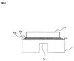
- Sectional drawing of the pressure detection apparatus which concerns on Embodiment 1 of this invention The enlarged view of the pressure detection apparatus shown in FIG.
- FIG. 1 is a cross-sectional view of a pressure detection device 100 according to Embodiment 1 of the present invention.
- the pressure detection device 100 of this embodiment is a pressure detection device that detects the pressure of, for example, brake oil for automobiles, and in particular, is a pressure detection device mounted with a Si chip that detects distortion.
- the pressure detection device 100 of the present embodiment is characterized by having the following configuration, for example.
- the pressure detection device 100 includes a pressure port 1 that is a metal housing having a pressure introduction portion and a diaphragm 1a that is deformed by the pressure of the pressure introduction portion, and a sensor element 4 that includes a Si chip that detects distortion of the diaphragm 1a.
- the diaphragm 1a and the sensor element 4 are bonded via a bonding glass layer 10a directly bonded to the sensor element 4 and a base glass layer 10b laminated between the bonding glass layer 10a and the diaphragm 1a. (See FIG. 2).
- the bonding glass layer 10a is a crystallized glass layer
- the base glass layer 10b includes at least one crystallized glass layer.
- the pressure detection device 100 includes a pressure port 1, a base 2, a cover 3, a sensor element 4, a housing 5, a connector terminal 6, a terminal block 7, a terminal 8, a silicone gel 9, and a bonding material 10. And a wire 11.
- the pressure port 1 which is a cylindrical metal housing has a pressure introduction part for introducing a pressure medium on the inside thereof and a diaphragm 1a serving as a pressure receiving surface which is deformed by the pressure of the pressure introduction part.
- the material of the pressure port 1 and the diaphragm 1a serving as the pressure receiving surface thereof is, for example, SUS630.
- the sensor element 4 is a one-chip type element in which a strain detection element and a processing circuit are formed on a silicon substrate, and a circuit board for laying out only the processing circuit unit is not necessary. That is, the sensor element 4 is a sensor element made of a Si chip, and is bonded via a bonding material 10 on the pedestal surface 1b located on the opposite side of the pressure introducing portion of the diaphragm 1a that is the pressure receiving surface of the pressure port 1. .
- the sensor element 4 detects distortion of the diaphragm 1a that is deformed by receiving pressure from the pressure medium, and outputs a pressure signal by the processing circuit.
- the base 2 is joined to the pressure port 1 by welding or the like.
- the terminal block 7 is formed integrally with the terminal 8 having a concave shape, and is fixed on the base 2 by, for example, an adhesive 12.
- the terminal 8 is connected to the sensor element 4 by a wire 11 formed by wire bonding.
- the silicone gel 9 is formed by potting or the like in order to protect the sensor element 4 connected to the terminal 8 by the wire 11 from foreign matter or the like.
- the housing 5 is formed integrally with the cover 3 and the connector terminal 6 having a hexagonal shape, for example, by insert molding.
- the connector terminal 6 is inserted into the concave shape portion of the terminal 8 and connected to the terminal 8.
- the cover 3 is joined and fixed to the base 2 by welding or the like, and is integrated with the base 2.
- the pressure detection device 100 detects the strain of the diaphragm 1a deformed by receiving pressure from the pressure medium by the strain detection element of the sensor element 4, and converts it into a pressure signal by the processing circuit of the sensor element 4.
- the pressure signal generated by the sensor element 4 is output to the outside via the wire 11, the terminal 8, and the connector terminal 6.
- FIG. 2 is an enlarged view of the pressure detection device 100 shown in FIG. In FIG. 2, illustration of the silicone gel 9 and the wire 11 is omitted.
- the bonding material 10 includes a bonding glass layer 10a that is directly bonded to the sensor element 4, and a base glass layer 10b that is laminated between the bonding glass layer 10a and the diaphragm 1a and that is a lower layer than the bonding glass layer 10a. Yes.
- the diaphragm 1a and the sensor element 4 are bonded through the bonding glass layer 10a bonded directly to the sensor element 4 and the base glass layer 10b laminated between the bonding glass layer 10a and the diaphragm 1a. ing.
- the bonding glass layer 10a is a crystallized glass layer formed of crystallized glass, and is preferably a low melting point crystallized glass layer formed of low melting point crystallized glass.
- the underlying glass layer 10b includes at least one crystallized glass layer. More specifically, in the pressure detection device 100 of the present embodiment, the single-layer base glass layer 10b is a crystallized glass layer formed of crystallized glass.
- the melting point of at least one crystallized glass layer included in the base glass layer 10b is preferably 800 ° C. or higher. More specifically, the base glass layer 10b, which is a crystallized glass layer, is preferably a high melting point crystallized glass layer formed of a high melting point crystallized glass such as celsian glass or ⁇ -spodumene glass.
- the diaphragm 1a and the sensor element 4 include the bonding glass layer 10a directly bonded to the sensor element 4, and the bonding glass layer 10a and the diaphragm 1a. Are bonded to each other through a base glass layer 10b laminated on the substrate. Therefore, the bonding glass layer 10a does not directly contact Cu deposited from the material of the diaphragm 1a such as SUS630. Thereby, the crystallization of the bonding glass layer 10a is suppressed, and the sensor element 4 made of the Si chip and the diaphragm 1a can be bonded stably.
- the base glass layer 10b includes at least one dense crystallized glass layer, the rigidity of the base glass layer 10b can be increased. Therefore, it is possible to relieve the thermal stress at the time of joining the diaphragm 1a and the sensor element 4 and improve the joining yield.
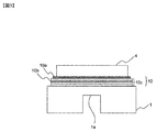
- FIG. 3 is an enlarged view corresponding to FIG. 2 of the pressure detection device according to the second embodiment of the present invention.
- the pressure detection device of the present embodiment is different from the pressure detection device 100 of Embodiment 1 described above in that the base glass layer 10c has a multilayer structure in which a plurality of glass layers are stacked. Since the other points of the pressure detection device of the present embodiment are the same as those of the pressure detection device 100 of the above-described first embodiment, the same portions are denoted by the same reference numerals and description thereof is omitted.
- the bonding material 10 is laminated between the bonding glass layer 10a and the diaphragm 1a below the bonding glass layer 10a and the bonding glass layer 10a bonded directly to the sensor element 4.
- the underlying glass layer 10c In other words, the diaphragm 1a and the sensor element 4 are bonded via the bonding glass layer 10a directly bonded to the sensor element 4 and the base glass layer 10c laminated between the bonding glass layer 10a and the diaphragm 1a. Has been.
- the bonding glass layer 10a is a crystallized glass layer similar to the pressure detection device 100 of the first embodiment described above.
- the base glass layer 10c made of a plurality of glass layers includes at least one crystallized glass layer 10b.
- At least one crystallized glass layer 10b included in the base glass layer 10c is a high melting point crystallized glass formed of, for example, celsian glass or ⁇ -spodumene glass, as in the pressure detection device 100 of the first embodiment.
- a layer is preferred.
- the same effects as those of the pressure detection device 100 of the first embodiment can be obtained. Further, since the base glass layer 10c has a multilayer structure in which a plurality of glass layers are laminated, the crystallization of the bonding glass layer 10a is more effectively suppressed, and the sensor element 4 and the diaphragm made of an Si chip are more stably suppressed. 1a can be joined.
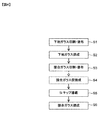
- FIG. 4 is a process diagram showing an example of a joining process of the sensor element 4 shown in FIGS. 2 and 3.
- the material of the base glass layers 10b and 10c is printed or applied to the diaphragm 1a of the pressure port 1 (process S1).
- the material of the ground glass layer 10b or the crystallized glass layer 10b included in the ground glass layer 10c is fired at a sufficient firing temperature to be crystallized, thereby forming the ground glass layers 10b and 10c (step S2).
- the material of the bonding glass layer 10a is printed or applied on the base glass layers 10b and 10c (step S3).
- the material of the bonding glass layer 10a is temporarily fired (step S4).
- omit process S4 when the material of the joining glass layer 10a does not contain an organic material.
- the Si chip of the sensor element 4 is mounted on the material of the bonding glass layer 10a or the material of the bonding glass layer 10a that has been baked (step S5). Then, the material of the bonding glass layer 10a on which the sensor element 4 is mounted or the material of the temporarily baked bonding glass layer 10a is baked and crystallized at a sufficient temperature (step S6).
- the diaphragm 1a and the sensor element 4 include the bonding glass layer 10a directly bonded to the sensor element 4, and the base glass layers 10b and 10c laminated between the bonding glass layer 10a and the diaphragm 1a. Are joined together.
- the joining process of the sensor element 4 is not limited to the process shown in FIG.
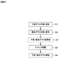
- FIG. 5 is a process diagram showing a modification of the joining process of the sensor element 4 shown in FIG.
- step S2 between step S1 and step S3 shown in FIG. 4 is omitted, and instead of step S4, temporary firing of the material of the bonding glass layer 10a and the material of the underlying glass layers 10b and 10c is performed at once.
- Step S7 can be abbreviate
- the Si chip of the sensor element 4 is mounted in the same manner as in the bonding step described above (step S5).
- the material of the bonding glass layer 10a on which the sensor element 4 is mounted and the material of the base glass layers 10b and 10c or these temporarily fired materials are fired at a sufficient temperature to be crystallized (step S8).
- the diaphragm 1a and the sensor element 4 include the bonding glass layer 10a directly bonded to the sensor element 4, and the base glass layers 10b and 10c laminated between the bonding glass layer 10a and the diaphragm 1a. Are joined together.
- the pressure detection device described in the above-described embodiment is mainly used for pressure detection in vehicles, but can be used in other industrial applications as well.
Landscapes
- Physics & Mathematics (AREA)
- General Physics & Mathematics (AREA)
- Measuring Fluid Pressure (AREA)
- Pressure Sensors (AREA)
Abstract
接合ガラスがCuと接して結晶化するのを防止してSiチップと金属ダイアフラムを接合可能な圧力検出装置を提供する。 圧力導入部と該圧力導入部の圧力により変形するダイアフラム1aとを有する圧力ポート1a(金属筐体)と、ダイアフラム1aの歪みを検出するSiチップから成るセンサ素子4とを備える圧力検出装置。ダイアフラム1aとセンサ素子4とは、該センサ素子4に直接接合される接合ガラス層10aと、該接合ガラス層10aとダイアフラム1aとの間に積層された下地ガラス層10bとを介して接合され、接合ガラス層10aは、結晶化ガラス層であり、下地ガラス層10bは、少なくとも一つの結晶化ガラス層を含む。
Description
本発明は、圧力検出装置に関する。
例えば、自動車などのブレーキやサスペンション、燃料等の油圧を制御する圧力センサは、圧力媒体を金属ダイアフラムで受圧し、その歪み量を歪みゲージや歪みセンサチップで検出する圧力センサが主流となっている。このうち、歪みゲージを半導体技術によりSiチップに形成した歪みセンサチップは接合材により金属ダイアフラムに接合されるが、接合材には金属はんだやガラスが用いられている。このうち接合材は、低クリープ特性に有利なガラスが主流である。また金属ダイアフラムは高耐力、耐腐食性が求められるため、SUS630が主流となっている。
圧力検出装置において、歪みを検出するSiチップの接合材は低クリープ特性に優れているガラスによって金属ダイアフラムに接合される構造であり、金属ダイアフラムは一般的にSUS630が用いられ、SUS630はCu析出型ステンレスである。Siチップと直接接合する接合ガラスが結晶化ガラスの場合、ガラスが結晶化する前の流動性が十分に確保された温度域にて接合を行うのが一般的であるが、接合ガラスが金属ダイアフラムのSUS630から析出したCuと反応することにより結晶化温度が低温化し、流動性が失われ、接合が取れなくなってしまう。
本発明は、前記課題に鑑みてなされたものであり、接合ガラスがCuと接して結晶化するのを防止してSiチップと金属ダイアフラムを接合することが可能な圧力検出装置を提供することを目的とする。
前記目的を達成すべく、本発明の圧力検出装置は、圧力導入部と該圧力導入部の圧力により変形するダイアフラムとを有する金属筐体と、前記ダイアフラムの歪みを検出するSiチップから成る歪み検出素子とを備える圧力検出装置において、前記ダイアフラムと前記歪み検出素子とは、該歪み検出素子に直接接合される接合ガラス層と、該接合ガラス層と前記ダイアフラムとの間に積層された下地ガラス層とを介して接合され、前記接合ガラス層は、結晶化ガラス層であり、前記下地ガラス層は、少なくとも一つの結晶化ガラス層を含むことを特徴とする。
上記の構成により、接合ガラス層が、例えばSUS630等のダイアフラムの素材から析出したCuと直接接しないことから、接合ガラス層が結晶化せず、安定してSiチップから成るセンサ素子とダイアフラムとを接合することが出来る。また下地ガラス層が少なくとも一つの緻密な結晶化ガラス層を含むことから、下地ガラス層の剛性を高めることが出来るため、接合時の熱応力を緩和し、接合歩留りを向上することが可能である。
以下、本発明の圧力検出装置の実施形態について、図面を参照して説明する。
[実施形態1]
図1は、本発明の実施形態1に係る圧力検出装置100の断面図である。本実施形態の圧力検出装置100は、例えば自動車用のブレーキオイル等の圧力を検出する圧力検出装置であり、特に、歪みを検出するSiチップを実装した圧力検出装置である。本実施形態の圧力検出装置100は、例えば、以下の構成を備えることを特徴としている。
図1は、本発明の実施形態1に係る圧力検出装置100の断面図である。本実施形態の圧力検出装置100は、例えば自動車用のブレーキオイル等の圧力を検出する圧力検出装置であり、特に、歪みを検出するSiチップを実装した圧力検出装置である。本実施形態の圧力検出装置100は、例えば、以下の構成を備えることを特徴としている。
すなわち、圧力検出装置100は、圧力導入部と該圧力導入部の圧力により変形するダイアフラム1aとを有する金属筐体である圧力ポート1と、ダイアフラム1aの歪みを検出するSiチップから成るセンサ素子4とを備える。上記のダイアフラム1aとセンサ素子4とは、センサ素子4に直接接合される接合ガラス層10aと、接合ガラス層10aとダイアフラム1aとの間に積層された下地ガラス層10bとを介して接合されている(図2参照)。さらに、接合ガラス層10aは、結晶化ガラス層であり、下地ガラス層10bは、少なくとも一つの結晶化ガラス層を含む。
以下、本実施形態の圧力検出装置100の全体構成について説明する。
圧力検出装置100は、圧力ポート1と、ベース2と、カバー3と、センサ素子4と、ハウジング5と、コネクタターミナル6と、端子台7と、ターミナル8と、シリコーンゲル9と、接合材10と、ワイヤ11とを備えている。筒状の金属筐体である圧力ポート1は、内側に圧力媒体を導入する圧力導入部を有するとともに、圧力導入部の圧力により変形する受圧面となるダイアフラム1aを有している。圧力ポート1及びその受圧面となるダイアフラム1aの素材は、例えばSUS630である。
センサ素子4は、歪み検出素子と処理回路とがシリコン基板上に形成された1チップ型の素子であり、処理回路部のみをレイアウトする回路基板は不要である。すなわち、センサ素子4は、Siチップから成るセンサ素子であり、圧力ポート1の受圧面であるダイアフラム1aの圧力導入部と反対側に位置する台座面1b上に接合材10を介して接合される。センサ素子4は、圧力媒体から圧力を受けて変形するダイアフラム1aの歪みを歪み検出素子によって検出し、処理回路によって圧力信号を出力する。
ベース2は、溶接等により圧力ポート1に接合される。端子台7は、凹形状を有するターミナル8と一体に形成され、例えば接着剤12によって、ベース2上に固定される。ターミナル8は、ワイヤボンディングによって形成されたワイヤ11によって、センサ素子4に接続される。ワイヤ11の素材としては、例えばAl又はAuを用いることができる。
シリコーンゲル9は、ワイヤ11によってターミナル8に接続されたセンサ素子4を異物等から保護するために、ポッティング等によって形成されている。ハウジング5は、例えばインサート成形によって、六角形状を有するカバー3及びコネクタターミナル6と一体に形成されている。コネクタターミナル6は、ターミナル8の凹形状部に挿入されてターミナル8に接続される。カバー3は、溶接等によりベース2に接合されて固定され、ベース2と一体化される。
以上の構成により、圧力検出装置100は、圧力媒体から圧力を受けて変形したダイアフラム1aの歪みを、センサ素子4の歪み検出素子によって検出し、センサ素子4の処理回路で圧力信号に変換する。センサ素子4によって生成された圧力信号は、ワイヤ11、ターミナル8、コネクタターミナル6を介して、外部に出力される。
図2は、図1に示す圧力検出装置100の拡大図である。なお、図2では、シリコーンゲル9及びワイヤ11等の図示を省略している。前述のように、圧力ポート1のダイアフラム1aとセンサ素子4とは、接合材10を介して接合されている。接合材10は、センサ素子4に直接接合される接合ガラス層10aと、接合ガラス層10aとダイアフラム1aとの間に積層され、接合ガラス層10aよりも下層となる下地ガラス層10bを有している。換言すると、ダイアフラム1aとセンサ素子4とは、センサ素子4に直接接合される接合ガラス層10aと、接合ガラス層10aとダイアフラム1aとの間に積層された下地ガラス層10bとを介して接合されている。
接合ガラス層10aは、結晶化ガラスによって形成された結晶化ガラス層であり、好ましくは、低融点結晶化ガラスによって形成された低融点結晶化ガラス層である。下地ガラス層10bは、少なくとも一つの結晶化ガラス層を含む。より具体的には、本実施形態の圧力検出装置100において、単層の下地ガラス層10bは、結晶化ガラスによって形成された結晶化ガラス層である。なお、下地ガラス層10bに含まれる少なくとも一つの結晶化ガラス層の融点は、800℃以上であることが好ましい。より具体的には、結晶化ガラス層である下地ガラス層10bは、好ましくは、セルシアン系ガラスやβスポジュメン系ガラス等の高融点結晶化ガラスによって形成された高融点結晶化ガラス層である。
以上のように、本実施形態の圧力検出装置100では、ダイアフラム1aとセンサ素子4とは、該センサ素子4に直接接合される接合ガラス層10aと、該接合ガラス層10aとダイアフラム1aとの間に積層された下地ガラス層10bとを介して接合されている。そのため、接合ガラス層10aが、例えばSUS630等のダイアフラム1aの素材から析出したCuと直接接しない。これにより、接合ガラス層10aの結晶化が抑制され、安定してSiチップから成るセンサ素子4とダイアフラム1aとを接合することが出来る。また、下地ガラス層10bが少なくとも一つの緻密な結晶化ガラス層を含むことから、下地ガラス層10bの剛性を高めることが出来る。したがって、ダイアフラム1aとセンサ素子4との接合時の熱応力を緩和し、接合歩留りを向上することが可能である。
[実施形態2]
以下、本発明の実施形態2について、図1を援用し、図3を用いて説明する。図3は、本発明の実施形態2に係る圧力検出装置の図2に相当する拡大図である。
以下、本発明の実施形態2について、図1を援用し、図3を用いて説明する。図3は、本発明の実施形態2に係る圧力検出装置の図2に相当する拡大図である。
本実施形態の圧力検出装置は、下地ガラス層10cが、複数のガラス層を積層した多層構造を有する点で、前述の実施形態1の圧力検出装置100と異なっている。本実施形態の圧力検出装置のその他の点は、前述の実施形態1の圧力検出装置100と同一であるので、同一の部分には同一の符号を付して説明を省略する。
本実施形態の圧力検出装置において、接合材10は、センサ素子4に直接接合される接合ガラス層10aと、接合ガラス層10aよりも下層で、接合ガラス層10aとダイアフラム1aとの間に積層された下地ガラス層10cから成る。換言すると、ダイアフラム1aとセンサ素子4とは、センサ素子4に直接接合される接合ガラス層10aと、該接合ガラス層10aとダイアフラム1aとの間に積層された下地ガラス層10cとを介して接合されている。
接合ガラス層10aは、前述の実施形態1の圧力検出装置100と同様の結晶化ガラス層である。また、複数のガラス層からなる下地ガラス層10cは、少なくとも一つの結晶化ガラス層10bを含む。下地ガラス層10cに含まれる少なくとも一つの結晶化ガラス層10bは、前述の実施形態1の圧力検出装置100と同様に、例えばセルシアン系ガラスやβスポジュメン系ガラス等によって形成された高融点結晶化ガラス層であることが好ましい。
本実施形態の圧力検出装置によれば、前述の実施形態1の圧力検出装置100と同様の効果を得ることができる。さらに、下地ガラス層10cが、複数のガラス層を積層した多層構造を有することで、接合ガラス層10aの結晶化がより効果的に抑制され、より安定してSiチップから成るセンサ素子4とダイアフラム1aとを接合することが出来る。
以下、前述の実施形態1に係る圧力検出装置100及び実施形態2に係る圧力検出装置の製造工程に含まれるセンサ素子4の接合工程の実施形態について説明する。図4は、図2及び図3に示すセンサ素子4の接合工程の一例を示す工程図である。
センサ素子4の接合工程においては、まず、下地ガラス層10b,10cの材料を圧力ポート1のダイアフラム1aに印刷又は塗布する(工程S1)。次に、下地ガラス層10b又は下地ガラス層10cに含まれる結晶化ガラス層10bの材料を十分な焼成温度で焼成して結晶化させ、下地ガラス層10b,10cを形成する(工程S2)。次に、接合ガラス層10aの材料を、下地ガラス層10b,10c上に印刷又は塗布する(工程S3)。次に、接合ガラス層10aの材料を仮焼成する(工程S4)。なお、工程S4は、接合ガラス層10aの材料が有機材を含まない場合には省略してもよい。
次に、接合ガラス層10aの材料上又は仮焼成した接合ガラス層10aの材料上にセンサ素子4のSiチップを搭載する(工程S5)。そして、センサ素子4を搭載した接合ガラス層10aの材料又は仮焼成した接合ガラス層10aの材料を十分な温度で焼成して結晶化させる(工程S6)。以上により、ダイアフラム1aとセンサ素子4とは、該センサ素子4に直接接合される接合ガラス層10aと、該接合ガラス層10aとダイアフラム1aとの間に積層された下地ガラス層10b,10cとを介して接合される。なお、センサ素子4の接合工程は、図4に示す工程に限定されない。
図5は、図4に示すセンサ素子4の接合工程の変形例を示す工程図である。
本変形例では、図4に示す工程S1と工程S3との間の工程S2を省略し、工程S4の代わりに、接合ガラス層10aの材料と下地ガラス層10b,10cの材料の仮焼成を一括して行っている(工程S7)。なお、工程S7は、接合ガラス層10aの材料と下地ガラス層10b,10cの材料が有機材を含まない場合には省略することができる。その後、前述の接合工程と同様に、センサ素子4のSiチップを搭載する(工程S5)。
最後に、センサ素子4を搭載した接合ガラス層10aの材料と下地ガラス層10b,10cの材料又は仮焼成したこれらの材料を十分な温度で焼成して結晶化させる(工程S8)。以上により、ダイアフラム1aとセンサ素子4とは、該センサ素子4に直接接合される接合ガラス層10aと、該接合ガラス層10aとダイアフラム1aとの間に積層された下地ガラス層10b,10cとを介して接合される。
以上、図面を用いて本発明の実施の形態を詳述してきたが、具体的な構成はこの実施形態に限定されるものではなく、本発明の要旨を逸脱しない範囲における設計変更等があっても、それらは本発明に含まれるものである。例えば、前述の実施形態において説明した圧力検出装置は、車輌での圧力検出が主な使用用途であるが、他の産業用途においても同様に利用が可能である。
1 圧力ポート(金属筐体)
1a ダイアフラム
1b 台座面
2 ベース
3 カバー
4 センサ素子
5 ハウジング
6 コネクタターミナル
7 端子台
8 ターミナル
9 シリコーンゲル
10 接合材
10a 接合ガラス層(結晶化ガラス層)
10b 下地ガラス層(結晶化ガラス層)
10c 下地ガラス層
11 ワイヤ
12 接着剤
1a ダイアフラム
1b 台座面
2 ベース
3 カバー
4 センサ素子
5 ハウジング
6 コネクタターミナル
7 端子台
8 ターミナル
9 シリコーンゲル
10 接合材
10a 接合ガラス層(結晶化ガラス層)
10b 下地ガラス層(結晶化ガラス層)
10c 下地ガラス層
11 ワイヤ
12 接着剤
Claims (6)
- 圧力導入部と該圧力導入部の圧力により変形するダイアフラムとを有する金属筐体と、前記ダイアフラムの歪みを検出するSiチップから成るセンサ素子とを備える圧力検出装置において、
前記ダイアフラムと前記センサ素子とは、該センサ素子に直接接合される接合ガラス層と、該接合ガラス層と前記ダイアフラムとの間に積層された下地ガラス層とを介して接合され、
前記接合ガラス層は、結晶化ガラス層であり、
前記下地ガラス層は、少なくとも一つの結晶化ガラス層を含むことを特徴とする圧力検出装置。 - 請求項1に記載の圧力検出装置において、前記下地ガラス層に含まれる少なくとも一つの前記結晶化ガラス層の融点は、800℃以上であることを特徴とする圧力検出装置。
- 請求項1に記載の圧力検出装置において、前記下地ガラス層に含まれる少なくとも一つの前記結晶化ガラス層は、セルシアン系ガラスであることを特徴とする圧力検出装置。
- 請求項1に記載の圧力検出装置において、前記下地ガラス層に含まれる少なくとも一つの前記結晶化ガラス層は、βスポジュメン系ガラスであることを特徴とする圧力検出装置。
- 請求項1に記載の圧力検出装置において、前記下地ガラス層は、複数のガラス層を積層した多層構造を有することを特徴とする圧力検出装置。
- 請求項1に記載の圧力検出装置において、前記ダイアフラムの素材は、SUS630であることを特徴とする圧力検出装置。
Priority Applications (1)
| Application Number | Priority Date | Filing Date | Title |
|---|---|---|---|
| JP2017547700A JP6457109B2 (ja) | 2015-10-28 | 2016-10-05 | 圧力検出装置 |
Applications Claiming Priority (2)
| Application Number | Priority Date | Filing Date | Title |
|---|---|---|---|
| JP2015-211401 | 2015-10-28 | ||
| JP2015211401 | 2015-10-28 |
Publications (1)
| Publication Number | Publication Date |
|---|---|
| WO2017073274A1 true WO2017073274A1 (ja) | 2017-05-04 |
Family
ID=58631475
Family Applications (1)
| Application Number | Title | Priority Date | Filing Date |
|---|---|---|---|
| PCT/JP2016/079562 Ceased WO2017073274A1 (ja) | 2015-10-28 | 2016-10-05 | 圧力検出装置 |
Country Status (2)
| Country | Link |
|---|---|
| JP (1) | JP6457109B2 (ja) |
| WO (1) | WO2017073274A1 (ja) |
Cited By (1)
| Publication number | Priority date | Publication date | Assignee | Title |
|---|---|---|---|---|
| CN112345125A (zh) * | 2019-08-06 | 2021-02-09 | 纬湃科技美国有限责任公司 | 用于增强厚膜压阻压力传感器灵敏度的密封玻璃几何结构 |
Families Citing this family (2)
| Publication number | Priority date | Publication date | Assignee | Title |
|---|---|---|---|---|
| JP6486866B2 (ja) * | 2016-05-27 | 2019-03-20 | 日立オートモティブシステムズ株式会社 | 物理量測定装置およびその製造方法ならびに物理量測定素子 |
| CN109990942A (zh) * | 2019-04-30 | 2019-07-09 | 芜湖天波光电技术研究院有限公司 | 一种高压共轨压力传感器 |
Citations (5)
| Publication number | Priority date | Publication date | Assignee | Title |
|---|---|---|---|---|
| JPS5057591A (ja) * | 1973-09-21 | 1975-05-20 | ||
| JPS535981A (en) * | 1976-07-06 | 1978-01-19 | Toyoda Chuo Kenkyusho Kk | Method of producing semiconductor device |
| JPH09301737A (ja) * | 1996-05-14 | 1997-11-25 | Iwaki Glass Kk | 単斜晶セルシアン含有結晶化ガラス及びその製造に好適な組成のガラスと製造方法 |
| JP2015114278A (ja) * | 2013-12-13 | 2015-06-22 | 株式会社デンソー | 圧力センサ |
| WO2015098324A1 (ja) * | 2013-12-25 | 2015-07-02 | 日立オートモティブシステムズ株式会社 | 圧力測定装置 |
Family Cites Families (1)
| Publication number | Priority date | Publication date | Assignee | Title |
|---|---|---|---|---|
| US7260994B2 (en) * | 2005-11-03 | 2007-08-28 | Honeywell International Inc. | Low cost high-pressure sensor |
-
2016
- 2016-10-05 JP JP2017547700A patent/JP6457109B2/ja active Active
- 2016-10-05 WO PCT/JP2016/079562 patent/WO2017073274A1/ja not_active Ceased
Patent Citations (5)
| Publication number | Priority date | Publication date | Assignee | Title |
|---|---|---|---|---|
| JPS5057591A (ja) * | 1973-09-21 | 1975-05-20 | ||
| JPS535981A (en) * | 1976-07-06 | 1978-01-19 | Toyoda Chuo Kenkyusho Kk | Method of producing semiconductor device |
| JPH09301737A (ja) * | 1996-05-14 | 1997-11-25 | Iwaki Glass Kk | 単斜晶セルシアン含有結晶化ガラス及びその製造に好適な組成のガラスと製造方法 |
| JP2015114278A (ja) * | 2013-12-13 | 2015-06-22 | 株式会社デンソー | 圧力センサ |
| WO2015098324A1 (ja) * | 2013-12-25 | 2015-07-02 | 日立オートモティブシステムズ株式会社 | 圧力測定装置 |
Cited By (2)
| Publication number | Priority date | Publication date | Assignee | Title |
|---|---|---|---|---|
| CN112345125A (zh) * | 2019-08-06 | 2021-02-09 | 纬湃科技美国有限责任公司 | 用于增强厚膜压阻压力传感器灵敏度的密封玻璃几何结构 |
| CN112345125B (zh) * | 2019-08-06 | 2022-10-14 | 纬湃科技美国有限责任公司 | 用于增强厚膜压阻压力传感器灵敏度的密封玻璃几何结构 |
Also Published As
| Publication number | Publication date |
|---|---|
| JP6457109B2 (ja) | 2019-01-23 |
| JPWO2017073274A1 (ja) | 2018-08-09 |
Similar Documents
| Publication | Publication Date | Title |
|---|---|---|
| US8704318B2 (en) | Encapsulation structure for silicon pressure sensor | |
| US8276460B2 (en) | Packaging for chip-on-board pressure sensor | |
| JP5064658B2 (ja) | 鋼ダイヤフラム上にシリコンチップを備えた圧力センサ | |
| JP5576331B2 (ja) | 圧力センサ装置 | |
| CN101957245B (zh) | 具有不受约束的敏感裸芯的传感器封装组件 | |
| JP5331546B2 (ja) | 圧力センサモジュール及び電子部品 | |
| CN106458575A (zh) | 包含微机电系统声敏感测器和环境感测器的集成封装件及其制造方法 | |
| KR20170102802A (ko) | 압력 센서 칩 및 압력 센서 | |
| JP6154488B2 (ja) | 圧力測定装置 | |
| JP6457109B2 (ja) | 圧力検出装置 | |
| US9835513B2 (en) | Sensor module for measuring a pressure of a fluid with at least one electronic circuit, particularly an integrated circuit, arranged on a circuit carrier, and at least one pressure measuring chip | |
| JP3915605B2 (ja) | 圧力センサ装置 | |
| US20110073969A1 (en) | Sensor system and method for manufacturing same | |
| US9983081B2 (en) | Pressure sensor | |
| JP2005127750A (ja) | 半導体センサおよびその製造方法 | |
| JP5971267B2 (ja) | 圧力センサおよびその製造方法 | |
| KR101573367B1 (ko) | 압저항형 세라믹 압력센서 | |
| JP2009265012A (ja) | 半導体センサ | |
| CN103728093A (zh) | 具有对抗安装应力的稳健性的压力传感器 | |
| JP6248009B2 (ja) | 圧力センサ | |
| JP6287600B2 (ja) | 温度センサ | |
| JP4069874B2 (ja) | センサ装置 | |
| JP4706634B2 (ja) | 半導体センサおよびその製造方法 | |
| JP7406947B2 (ja) | センサチップ | |
| JP6760029B2 (ja) | 温度センサ |
Legal Events
| Date | Code | Title | Description |
|---|---|---|---|
| 121 | Ep: the epo has been informed by wipo that ep was designated in this application |
Ref document number: 16859511 Country of ref document: EP Kind code of ref document: A1 |
|
| ENP | Entry into the national phase |
Ref document number: 2017547700 Country of ref document: JP Kind code of ref document: A |
|
| NENP | Non-entry into the national phase |
Ref country code: DE |
|
| 122 | Ep: pct application non-entry in european phase |
Ref document number: 16859511 Country of ref document: EP Kind code of ref document: A1 |