WO2017061273A1 - 撮像装置、製造方法 - Google Patents
撮像装置、製造方法 Download PDFInfo
- Publication number
- WO2017061273A1 WO2017061273A1 PCT/JP2016/077789 JP2016077789W WO2017061273A1 WO 2017061273 A1 WO2017061273 A1 WO 2017061273A1 JP 2016077789 W JP2016077789 W JP 2016077789W WO 2017061273 A1 WO2017061273 A1 WO 2017061273A1
- Authority
- WO
- WIPO (PCT)
- Prior art keywords
- light receiving
- electrode
- receiving element
- signal processing
- processing circuit
- Prior art date
- Legal status (The legal status is an assumption and is not a legal conclusion. Google has not performed a legal analysis and makes no representation as to the accuracy of the status listed.)
- Ceased
Links
Images




Classifications
-
- H—ELECTRICITY
- H10—SEMICONDUCTOR DEVICES; ELECTRIC SOLID-STATE DEVICES NOT OTHERWISE PROVIDED FOR
- H10F—INORGANIC SEMICONDUCTOR DEVICES SENSITIVE TO INFRARED RADIATION, LIGHT, ELECTROMAGNETIC RADIATION OF SHORTER WAVELENGTH OR CORPUSCULAR RADIATION
- H10F39/00—Integrated devices, or assemblies of multiple devices, comprising at least one element covered by group H10F30/00, e.g. radiation detectors comprising photodiode arrays
- H10F39/80—Constructional details of image sensors
- H10F39/811—Interconnections
-
- G—PHYSICS
- G01—MEASURING; TESTING
- G01J—MEASUREMENT OF INTENSITY, VELOCITY, SPECTRAL CONTENT, POLARISATION, PHASE OR PULSE CHARACTERISTICS OF INFRARED, VISIBLE OR ULTRAVIOLET LIGHT; COLORIMETRY; RADIATION PYROMETRY
- G01J1/00—Photometry, e.g. photographic exposure meter
- G01J1/02—Details
-
- G—PHYSICS
- G01—MEASURING; TESTING
- G01J—MEASUREMENT OF INTENSITY, VELOCITY, SPECTRAL CONTENT, POLARISATION, PHASE OR PULSE CHARACTERISTICS OF INFRARED, VISIBLE OR ULTRAVIOLET LIGHT; COLORIMETRY; RADIATION PYROMETRY
- G01J1/00—Photometry, e.g. photographic exposure meter
- G01J1/42—Photometry, e.g. photographic exposure meter using electric radiation detectors
- G01J1/4228—Photometry, e.g. photographic exposure meter using electric radiation detectors arrangements with two or more detectors, e.g. for sensitivity compensation
-
- G—PHYSICS
- G01—MEASURING; TESTING
- G01J—MEASUREMENT OF INTENSITY, VELOCITY, SPECTRAL CONTENT, POLARISATION, PHASE OR PULSE CHARACTERISTICS OF INFRARED, VISIBLE OR ULTRAVIOLET LIGHT; COLORIMETRY; RADIATION PYROMETRY
- G01J5/00—Radiation pyrometry, e.g. infrared or optical thermometry
- G01J5/02—Constructional details
- G01J5/0225—Shape of the cavity itself or of elements contained in or suspended over the cavity
- G01J5/024—Special manufacturing steps or sacrificial layers or layer structures
-
- G—PHYSICS
- G01—MEASURING; TESTING
- G01J—MEASUREMENT OF INTENSITY, VELOCITY, SPECTRAL CONTENT, POLARISATION, PHASE OR PULSE CHARACTERISTICS OF INFRARED, VISIBLE OR ULTRAVIOLET LIGHT; COLORIMETRY; RADIATION PYROMETRY
- G01J5/00—Radiation pyrometry, e.g. infrared or optical thermometry
- G01J5/02—Constructional details
- G01J5/04—Casings
- G01J5/041—Mountings in enclosures or in a particular environment
- G01J5/045—Sealings; Vacuum enclosures; Encapsulated packages; Wafer bonding structures; Getter arrangements
-
- G—PHYSICS
- G01—MEASURING; TESTING
- G01J—MEASUREMENT OF INTENSITY, VELOCITY, SPECTRAL CONTENT, POLARISATION, PHASE OR PULSE CHARACTERISTICS OF INFRARED, VISIBLE OR ULTRAVIOLET LIGHT; COLORIMETRY; RADIATION PYROMETRY
- G01J5/00—Radiation pyrometry, e.g. infrared or optical thermometry
- G01J5/02—Constructional details
- G01J5/04—Casings
- G01J5/048—Protective parts
-
- G—PHYSICS
- G01—MEASURING; TESTING
- G01J—MEASUREMENT OF INTENSITY, VELOCITY, SPECTRAL CONTENT, POLARISATION, PHASE OR PULSE CHARACTERISTICS OF INFRARED, VISIBLE OR ULTRAVIOLET LIGHT; COLORIMETRY; RADIATION PYROMETRY
- G01J5/00—Radiation pyrometry, e.g. infrared or optical thermometry
- G01J5/10—Radiation pyrometry, e.g. infrared or optical thermometry using electric radiation detectors
- G01J5/20—Radiation pyrometry, e.g. infrared or optical thermometry using electric radiation detectors using resistors, thermistors or semiconductors sensitive to radiation, e.g. photoconductive devices
-
- G—PHYSICS
- G01—MEASURING; TESTING
- G01J—MEASUREMENT OF INTENSITY, VELOCITY, SPECTRAL CONTENT, POLARISATION, PHASE OR PULSE CHARACTERISTICS OF INFRARED, VISIBLE OR ULTRAVIOLET LIGHT; COLORIMETRY; RADIATION PYROMETRY
- G01J5/00—Radiation pyrometry, e.g. infrared or optical thermometry
- G01J5/10—Radiation pyrometry, e.g. infrared or optical thermometry using electric radiation detectors
- G01J5/20—Radiation pyrometry, e.g. infrared or optical thermometry using electric radiation detectors using resistors, thermistors or semiconductors sensitive to radiation, e.g. photoconductive devices
- G01J5/22—Electrical features thereof
- G01J5/24—Use of specially adapted circuits, e.g. bridge circuits
-
- H—ELECTRICITY
- H04—ELECTRIC COMMUNICATION TECHNIQUE
- H04N—PICTORIAL COMMUNICATION, e.g. TELEVISION
- H04N23/00—Cameras or camera modules comprising electronic image sensors; Control thereof
- H04N23/20—Cameras or camera modules comprising electronic image sensors; Control thereof for generating image signals from infrared radiation only
-
- H—ELECTRICITY
- H04—ELECTRIC COMMUNICATION TECHNIQUE
- H04N—PICTORIAL COMMUNICATION, e.g. TELEVISION
- H04N25/00—Circuitry of solid-state image sensors [SSIS]; Control thereof
- H04N25/70—SSIS architectures; Circuits associated therewith
-
- H—ELECTRICITY
- H10—SEMICONDUCTOR DEVICES; ELECTRIC SOLID-STATE DEVICES NOT OTHERWISE PROVIDED FOR
- H10F—INORGANIC SEMICONDUCTOR DEVICES SENSITIVE TO INFRARED RADIATION, LIGHT, ELECTROMAGNETIC RADIATION OF SHORTER WAVELENGTH OR CORPUSCULAR RADIATION
- H10F30/00—Individual radiation-sensitive semiconductor devices in which radiation controls the flow of current through the devices, e.g. photodetectors
- H10F30/20—Individual radiation-sensitive semiconductor devices in which radiation controls the flow of current through the devices, e.g. photodetectors the devices having potential barriers, e.g. phototransistors
-
- H—ELECTRICITY
- H10—SEMICONDUCTOR DEVICES; ELECTRIC SOLID-STATE DEVICES NOT OTHERWISE PROVIDED FOR
- H10F—INORGANIC SEMICONDUCTOR DEVICES SENSITIVE TO INFRARED RADIATION, LIGHT, ELECTROMAGNETIC RADIATION OF SHORTER WAVELENGTH OR CORPUSCULAR RADIATION
- H10F39/00—Integrated devices, or assemblies of multiple devices, comprising at least one element covered by group H10F30/00, e.g. radiation detectors comprising photodiode arrays
- H10F39/011—Manufacture or treatment of image sensors covered by group H10F39/12
- H10F39/021—Manufacture or treatment of image sensors covered by group H10F39/12 of image sensors having active layers comprising only Group III-V materials, e.g. GaAs, AlGaAs or InP
-
- H—ELECTRICITY
- H10—SEMICONDUCTOR DEVICES; ELECTRIC SOLID-STATE DEVICES NOT OTHERWISE PROVIDED FOR
- H10F—INORGANIC SEMICONDUCTOR DEVICES SENSITIVE TO INFRARED RADIATION, LIGHT, ELECTROMAGNETIC RADIATION OF SHORTER WAVELENGTH OR CORPUSCULAR RADIATION
- H10F39/00—Integrated devices, or assemblies of multiple devices, comprising at least one element covered by group H10F30/00, e.g. radiation detectors comprising photodiode arrays
- H10F39/10—Integrated devices
- H10F39/12—Image sensors
- H10F39/18—Complementary metal-oxide-semiconductor [CMOS] image sensors; Photodiode array image sensors
- H10F39/184—Infrared image sensors
- H10F39/1847—Multispectral infrared image sensors having a stacked structure, e.g. NPN, NPNPN or multiple quantum well [MQW] structures
-
- G—PHYSICS
- G01—MEASURING; TESTING
- G01J—MEASUREMENT OF INTENSITY, VELOCITY, SPECTRAL CONTENT, POLARISATION, PHASE OR PULSE CHARACTERISTICS OF INFRARED, VISIBLE OR ULTRAVIOLET LIGHT; COLORIMETRY; RADIATION PYROMETRY
- G01J1/00—Photometry, e.g. photographic exposure meter
- G01J1/42—Photometry, e.g. photographic exposure meter using electric radiation detectors
- G01J1/429—Photometry, e.g. photographic exposure meter using electric radiation detectors applied to measurement of ultraviolet light
-
- G—PHYSICS
- G01—MEASURING; TESTING
- G01J—MEASUREMENT OF INTENSITY, VELOCITY, SPECTRAL CONTENT, POLARISATION, PHASE OR PULSE CHARACTERISTICS OF INFRARED, VISIBLE OR ULTRAVIOLET LIGHT; COLORIMETRY; RADIATION PYROMETRY
- G01J5/00—Radiation pyrometry, e.g. infrared or optical thermometry
- G01J2005/0077—Imaging
-
- H—ELECTRICITY
- H04—ELECTRIC COMMUNICATION TECHNIQUE
- H04N—PICTORIAL COMMUNICATION, e.g. TELEVISION
- H04N25/00—Circuitry of solid-state image sensors [SSIS]; Control thereof
- H04N25/70—SSIS architectures; Circuits associated therewith
- H04N25/76—Addressed sensors, e.g. MOS or CMOS sensors
-
- H—ELECTRICITY
- H10—SEMICONDUCTOR DEVICES; ELECTRIC SOLID-STATE DEVICES NOT OTHERWISE PROVIDED FOR
- H10F—INORGANIC SEMICONDUCTOR DEVICES SENSITIVE TO INFRARED RADIATION, LIGHT, ELECTROMAGNETIC RADIATION OF SHORTER WAVELENGTH OR CORPUSCULAR RADIATION
- H10F99/00—Subject matter not provided for in other groups of this subclass
-
- H—ELECTRICITY
- H10—SEMICONDUCTOR DEVICES; ELECTRIC SOLID-STATE DEVICES NOT OTHERWISE PROVIDED FOR
- H10W—GENERIC PACKAGES, INTERCONNECTIONS, CONNECTORS OR OTHER CONSTRUCTIONAL DETAILS OF DEVICES COVERED BY CLASS H10
- H10W20/00—Interconnections in chips, wafers or substrates
- H10W20/01—Manufacture or treatment
- H10W20/021—Manufacture or treatment of interconnections within wafers or substrates
- H10W20/023—Manufacture or treatment of interconnections within wafers or substrates the interconnections being through-semiconductor vias
-
- H—ELECTRICITY
- H10—SEMICONDUCTOR DEVICES; ELECTRIC SOLID-STATE DEVICES NOT OTHERWISE PROVIDED FOR
- H10W—GENERIC PACKAGES, INTERCONNECTIONS, CONNECTORS OR OTHER CONSTRUCTIONAL DETAILS OF DEVICES COVERED BY CLASS H10
- H10W20/00—Interconnections in chips, wafers or substrates
- H10W20/20—Interconnections within wafers or substrates, e.g. through-silicon vias [TSV]
Definitions
- This technology relates to an imaging device and a manufacturing method. Specifically, the present invention relates to an imaging device having a light receiving sensitivity in an infrared region and a manufacturing method.
- a readout electrode of a signal readout silicon IC (ROIC: Read Out IC) and an electrode of the photodiode face each other, and a bump interposed between both faces. Conduction is taken. Since the photodiode is formed of a compound semiconductor in the infrared region longer than the visible region, it may be referred to as a hybrid configuration of a compound semiconductor and silicon (IC).
- the photodiode needs to be formed of a compound semiconductor, so there are restrictions on the material used for the bump, for example.
- the height of the bumps is likely to vary and short-circuiting is likely to occur, making it difficult to control and making arraying and miniaturization difficult.
- the electrode that collects carriers is on the surface opposite to the light receiving surface, and before the carrier photoelectrically converted on the surface of the light receiving surface reaches the electrode, There was a possibility that the recombination would reduce the sensitivity.
- the present technology has been made in view of such a situation, and even when a photodiode is formed of a compound semiconductor, it can be arrayed and miniaturized, and can prevent a decrease in sensitivity. It is what you want to do.
- An imaging apparatus includes a light receiving element array in which a plurality of light receiving elements made of a compound semiconductor having a light receiving sensitivity in an infrared region are arranged, a signal processing circuit that processes a signal from the light receiving element, and the light receiving element
- a light receiving element array in which a plurality of light receiving elements made of a compound semiconductor having a light receiving sensitivity in an infrared region are arranged, a signal processing circuit that processes a signal from the light receiving element, and the light receiving element
- the upper electrode and the signal processing circuit are connected to each other through a through via penetrating a part thereof, and the lower electrode is an electrode common to the light receiving elements arranged in the light receiving element array.
- the compound semiconductor may be a group III-V semiconductor.
- the lower electrode and the electrode can be connected via a through via penetrating to the electrode provided in the lower part of the light receiving element.
- the lower electrode may be connected to an electrode provided below the light receiving element at an outer peripheral portion of the light receiving element array.
- the lower electrode may be connected to the signal processing circuit at the outer periphery of the light receiving element array.
- the through via may be covered with a fixed charge film, and a part of the upper electrode may be laminated on the fixed charge film.
- a manufacturing method includes a light receiving element array in which a plurality of light receiving elements made of a compound semiconductor having a light receiving sensitivity in an infrared region are arranged, a signal processing circuit that processes a signal from the light receiving element, and the light receiving element
- a manufacturing method of manufacturing an imaging device including an upper electrode formed on the light receiving surface side and a lower electrode paired with the upper electrode, the light receiving element array and the signal processing circuit are formed of a film of a predetermined material. And forming a through via that penetrates a part of the light receiving element, connecting the upper electrode and the signal processing circuit via the through via, and receiving the lower electrode arranged in the light receiving element array. Forming a common electrode in the device.
- the compound semiconductor may be a group III-V semiconductor.
- the method further includes the steps of forming an electrode under the light receiving element, forming a through via penetrating to a top surface of the electrode in a part of the light receiving element, and connecting the lower electrode and the electrode through the through via.
- the method may further include a step of connecting the lower electrode to an electrode provided at a lower portion of the light receiving element at an outer peripheral portion of the light receiving element array.
- the method may further include a step of connecting the lower electrode to the signal processing circuit at an outer periphery of the light receiving element array.
- a light receiving element array in which a plurality of light receiving elements made of a compound semiconductor having light receiving sensitivity in the infrared region are arranged, a signal processing circuit that processes a signal from the light receiving element,
- the upper electrode formed in the light-receiving surface side and the lower electrode which makes a pair with an upper electrode are provided.
- the light receiving element array and the signal processing circuit are joined by a film of a predetermined material, and the upper electrode and the signal processing circuit are connected through a through via penetrating a part of the light receiving element, and the lower electrode
- the electrodes are common to the light receiving elements arranged in the element array.
- the imaging device is manufactured.
- a photodiode even when a photodiode is formed of a compound semiconductor, it can be arrayed or miniaturized, and a reduction in sensitivity can be prevented.
- the present technology can be applied to an imaging apparatus including an infrared image sensor.
- the imaging device for example, a device that detects a person or an object can be used.
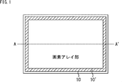
- the imaging device includes a pixel array unit 10 in the light receiving layer area.
- the pixel array unit 10 a plurality of pixels are arranged in an array.
- the pixels arranged in the pixel array unit 10 are light receiving elements made of a compound semiconductor having light receiving sensitivity in the infrared region.
- a signal processing circuit (not shown in FIG. 1) for reading out a signal from a pixel (light receiving element) arranged in the pixel array unit 10 is stacked below the light receiving layer area.
- Pixels arranged in the outer peripheral portion of the light receiving layer area (the portion indicated by hatching in FIG. 1 and hereinafter referred to as the pixel array portion 10 ') and the area other than the outer peripheral portion of the light receiving layer area It has a configuration that is partially different from the pixels arranged in (in FIG. 1, the area located inside the hatched portion).
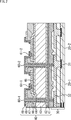
- FIG. 2 shows a configuration of pixels arranged in an area other than the outer peripheral portion of the light receiving layer area, and shows, for example, a cross-sectional view taken along a line A-A ′ in FIG.
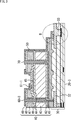
- FIG. 3 shows the configuration of the pixels arranged in the outer peripheral portion (pixel array portion 10 ′) of the light receiving layer area, and represents a cross-sectional view taken along the line A-A ′ in FIG. 1, for example.
- FIG. 2 shows the pixels 20-1 and 20-2 arranged in the light receiving layer area.
- the pixel 20-1 and the pixel 20-2 are simply referred to as the pixel 20 when it is not necessary to distinguish them individually. The other parts are described similarly.
- the pixel 20 has a configuration in which a signal processing circuit 30 and an infrared image sensor 40 are stacked.
- the infrared image sensor 40 functions as a light receiving element.
- the signal processing circuit 30 can be a circuit called ROIC (readout integrated circuit) or the like, and performs reading of the signal photoelectrically converted by the infrared image sensor 40 and processing of the read signal.
- ROIC readout integrated circuit
- a wiring layer including the electrode 31 and the wiring 32 connected to the infrared image sensor 40 is formed.
- the electrode 31 is made of, for example, Cu (copper), and the wiring 32 is made of Al (aluminum).
- the infrared image sensor 40 is bonded to the signal processing circuit 30 on the substrate.
- SiO2 silicon dioxide
- An electrode 41 is first laminated on the signal processing circuit 30 side of the infrared image sensor 40.
- the electrode 41 is made of, for example, W (tungsten) or Ti (titanium). As will be described later with reference to FIG. 3, the electrode 41 is connected to the grounded lower electrode 50 and provided as a pair with the upper electrode 49.
- n-InP layer (n-InAlAs layer) 42 is stacked on the upper layer of the electrode 41, and an i-InGaAs layer 43 that functions as a part of the light receiving layer is stacked on the n-InP layer 42.
- the light receiving layer includes an InGaAs layer, for example, a type 2 InGaAs / GaAsSb multiple quantum well structure may be used. Since the InGaAs layer has a small band gap, it can receive infrared light alone.
- a P-InP layer 44 is laminated in the opened portion on the i-InGaAs layer 43.
- ITO 45 is laminated as a transparent electrode.
- a protective film 46 is laminated on the ITO 45.
- An insulating film 47 is laminated at a place other than the opening on the protective film 46.
- This insulating film 47 can be formed of SiO2.
- a protective film 48 is laminated, and an upper electrode 49 is further laminated.
- the upper electrode 49 is connected to the ITO 45.
- Through-holes 60 are formed between the pixels 20.
- the through via 60-1 is formed on the left side of the pixel 20-1, and the through via 60-2 is formed on the right side.
- An upper electrode 49 and a protective film 48 are formed on the side surface of the through via 60.
- the upper electrode 49 is formed at the central portion of the through via 60, and the protective film 48 is formed on the inner side (the light receiving layer side) of the upper electrode 49.
- the protective film 48 functions as an insulating film and has a structure in which an insulating film is formed between the light receiving layer and the upper electrode 49 inside the through via 60.
- the upper electrode 49 formed in the through via 60 shown in FIG. 2 is shown with a gap, but the upper electrode 49 may be formed without a gap. In other words, the through via 60 may be filled with the material of the upper electrode 49.
- the protective film 46 and the protective film 48 may be made of the same material or different materials.
- the protective film 46 and the protective film 48 can be made of, for example, HfO, AlO, TaO, SiN, or SiON.
- the protective film covering the through via 60 becomes the protective film 48 because the pixel 20 is manufactured in a manufacturing process described later.
- the protective film covering the through via 60 can be a fixed charge film having a negative bias, and the fixed charge film can be a film formed of HfO, AlO, TaO, SiN, or SiON.
- One of the upper electrodes 49 is connected to the wiring 32 in the signal processing circuit 30 and the other is connected to the ITO 45.
- the upper electrode 49 and the ITO 45 are connected through a through via 61.
- the through via 61 is configured to penetrate the protective film 46 of the infrared image sensor 40, and the upper electrode 49 is connected to the ITO 45 by filling the material of the upper electrode 49 in the through via 61 that is penetrated. .
- the upper electrode 49 is an electrode for collecting charges photoelectrically converted by the light receiving layer (i-InGaAs layer 43). Light enters from above in FIG. 2 and is received by the light receiving layer. By providing the upper electrode 49 on the light incident side (light receiving surface side), carriers photoelectrically converted on the surface of the light receiving layer can be efficiently collected, and the sensitivity can be improved.
- the upper electrode 49 of each pixel 20 penetrates the infrared image sensor 40 (light receiving layer) and is formed in the signal processing circuit 30 by the through via 60 formed up to the surface of the wiring 32 in the signal processing circuit 30. It is connected to the wiring 32.
- the lower electrode that makes a pair with the upper electrode 49 is provided in the pixel disposed in the outer peripheral portion (pixel array unit 10 ′) of the pixel array unit 10.
- FIG. 3 shows a configuration of pixels arranged on the outer peripheral portion (pixel array portion 10 ′) of the light receiving area, for example, a cross-sectional view taken along the line A-A ′ in FIG. 1.
- FIG. 3 illustrates the pixel 20-3 located in the pixel array portion 10 '.
- the configuration of the pixel 20-3 is different from the pixel 20-1 shown in FIG. 2 in that the lower electrode 50 is provided, and the other portions are the same. Omitted.
- the through via 70 provided on the outer peripheral portion side (right side in the drawing) of the pixel 20-3 has a different structure from the through via 60 provided in an area other than the outer peripheral portion.
- the through via 70 does not penetrate the infrared image sensor 40 (light receiving layer) and is provided up to the electrode 41 constituting the infrared image sensor 40.
- a lower electrode 50 and a protective film 48 are formed in the through via 70.
- the lower electrode 50 is connected to the electrode 41 by being formed in the through via 70. That is, the electrode 41 functions as a lower electrode by being connected to the lower electrode 50 and is provided as a part of the lower electrode 50.
- the through via 60 shown on the left side of the pixel 20-3 shown in FIG. 3 is compared with the through via 70 shown on the right side.
- the through via 60 penetrates the infrared image sensor 40, and an upper electrode 49 and a protective film 48 are formed therein. Since the protective film 48 is formed between the upper electrode 49 and the electrode 41, the upper electrode 49 and the electrode 41 are not connected.
- the through via 70 does not penetrate the infrared image sensor 40, and a lower electrode 50 and a protective film 48 are formed inside the through via 70.
- the lower electrode 50 is connected to the electrode 41. Therefore, the electrode 41 constitutes a part of the lower electrode 50.
- the pixel 20 constituting the pixel array unit 10 is configured such that the upper electrode 49 is formed in the upper portion and the lower electrode 50 (electrode 41) is formed in the lower portion.
- the lower electrode 50 is connected to the wiring 33 in the signal processing circuit 30 at the terminal portion of the pixel array portion 10 ′ (portion B on the right side in FIG. 3 and surrounded by a dotted circle).
- the wiring 33 connected to the lower electrode 50 is grounded.
- the through via 70 may be provided to connect the lower electrode 50 and the electrode 41. However, as shown in FIG. It can also be set as the structure to which the electrode 41 is connected.
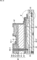
- the pixel 20-3 ′ shown in FIG. 4 is a pixel provided in the pixel array section 10 ′, but has a configuration in which the through via 70 for connecting the electrode 41 and the lower electrode 50 is not formed. .
- the pixel shown in FIG. 4 is given a dash and is described as a pixel 20-3 '.
- the other parts are also described in the same manner. However, when it is not necessary to distinguish the pixel 20-3 'and the pixel 20-3, they are simply described as the pixel 20-3.
- the pixel 20-3 ′ illustrated in FIG. 4 has the same structure as the pixel 20-3 disposed in an area other than the outer peripheral portion of the pixel array unit 10, but the outer peripheral side of the pixel array unit 10 On the right side (in FIG. 4), the through via 70 is not formed.
- the lower electrode 50 ′ is connected to the grounded wiring 33 at the terminal portion of the pixel array portion 10 ′. Referring to the portion B ′ in FIG. 4, the lower electrode 50 ′ is connected to the wiring 33 in the signal processing circuit 30 at the terminal portion of the pixel array portion 10 ′. The lower electrode 50 and the electrode 41 ′ in the infrared image sensor 40 are also connected at the terminal portion of the pixel array portion 10 ′.
- the electrode 41 ′ of the infrared image sensor 40 extends to the end portion (portion B ′) of the pixel array section 10, and in other words, the lower electrode at the end portion, that is, the portion outside the side surface of the pixel 20-3 ′. 50 '. In this manner, the lower electrode 50 ′, the electrode 41 ′, and the wiring 33 can be connected at the terminal portion of the pixel array unit 10.
- the lower electrode 50 as a common electrode for the plurality of pixels 20, it is possible to reduce the size. Also, the aperture ratio of each pixel 20 can be increased.
- the upper electrode 49 is connected to the wiring 32 in the signal processing circuit 30 by the through via 60
- the lower electrode 50 is connected to the electrode 41 in the infrared image sensor 40 by the through via 70, and signal processing is performed at the terminal portion. It is connected to the wiring 33 in the circuit 30 and grounded.
- the lower electrode 50 ′ is connected to the electrode 41 ′ in the infrared image sensor 40 at the terminal portion, connected to the wiring 33 ′ in the signal processing circuit 30, and grounded.
- a through via is formed at a position as shown in FIG. 5 or FIG. 6, and a P-InP layer 44 is formed.
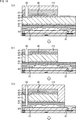
- FIG. 5 is a cross-sectional view of a pixel when the pixels are separated by mesa separation and a plan view when viewed from above.
- the cross-sectional view of the pixel 20 shown in FIG. 5A is the same as the cross-sectional view of the pixel 20 shown in FIG.
- FIG. 5B is a plan view of the pixel 20 shown in FIG. 5A when viewed from the light-receiving surface side, and shows the positions of vias and the area of the P-InP layer 44. In FIG. 5B, 2 ⁇ 2 4 pixels are shown.
- a separation unit 80 is provided and separated between each of the pixel 20-1, the pixel 20-2, the pixel 20-11, and the pixel 20-12.
- a through via 60-1 is formed on the lower left side of the pixel 20-1, and a through via 61-1 is formed on the right side thereof.
- the upper electrode 49 is formed on the through via 60-1 and the through via 61-1, and is also formed between the pixels 20. However, the upper electrode 49 is formed independently without contacting the other upper electrode 49. ing.
- FIG. 6 is a cross-sectional view of a pixel when the pixels are separated by planar separation and a plan view when viewed from above.
- the cross-sectional view of the pixel 20 shown in FIG. 6A is substantially the same as the cross-sectional view of the pixel 20 shown in FIG.
- the pixel 20 shown in FIG. 6A is different from the pixel 20 shown in FIG. 5A in that the P-InP layer 44 is provided between the through vias 60 and is not divided by the protective film 46.
- FIG. 6B is a plan view of the pixel 20 shown in FIG. 6A when viewed from the light-receiving surface side, and shows the positions of vias and the area of the P-InP layer 44.
- FIG. FIG. 6B shows 2 ⁇ 2 4 pixels. 5 differs from the pixel 20 shown in FIG. 5B in that the P-InP layer 44 is connected in a portion other than the through via 60-1. Note that the pixels 20 are separated by impurities.
- the light receiving layer area can be enlarged.
- the present technology can be applied to both separation methods of mesa separation and planar separation. Further, the present technology can be applied to separation methods other than these.
- the through via 60 and the through via 61 are each shown as a quadrangle, but may have other shapes such as a circle.
- a substrate is prepared.
- an N-InGaAs layer 102 as a buffer layer is formed on an n-InP layer 101 as a support substrate, and a P-InP layer 44, an i-InGaAs layer 43, and an n ⁇ An InP (n-InAlAs) layer 42 is formed in this order.
- the substrate can be formed by a crystal growth method or the like.
- step S2 an electrode to be the upper electrode 49 is formed on the substrate, and an insulating film (oxide film) 103 is formed on the electrode.
- the electrode is formed of a material such as W (tungsten) or Ti (titanium), and the insulating film 103 is formed of a material such as SiO 2 (silicon dioxide).
- step S3 the substrate (infrared image sensor 40) and the signal processing circuit 30 (ROIC substrate) are bonded together.
- the insulating film 103 formed on the lower surface of the infrared image sensor 40 and the upper surface of the signal processing circuit 30 are bonded with an adhesive.
- the infrared image sensor 40 may be provided with the insulating film 103, and the insulating film 103 and the signal processing circuit 30 may be bonded together. However, the bonding is performed without providing the insulating film 103. Also good.
- the infrared image sensor 40 and the signal processing circuit 30 are bonded to each other with a predetermined adhesive or the like, and there is no process of bonding with a bump or the like.
- the infrared image sensor 40 and the signal processing circuit 30 are made of different materials.
- the infrared image sensor 40 is formed of a compound semiconductor such as InGaAs
- the signal processing circuit 30 is formed of a material such as silicon (Si).
- the infrared image sensor 40 and the signal processing circuit 30 are formed of different materials, if they are joined by bumps, there are restrictions on the materials that can be used for the bumps. Also, due to such restrictions, bump heights are likely to vary, and short-circuiting is likely to occur, making it difficult to control and making arraying and miniaturization difficult.
- the infrared image sensor 40 and the signal processing circuit 30 are attached not by bumps but by adhesion between substrates, the above-described problems occur when bumps are used. However, it is possible to realize arraying and miniaturization.
- bumps are not used, there are no restrictions on materials when bumps are used, and the degree of freedom in selecting materials for the bonding surfaces of the infrared image sensor 40 and the signal processing circuit 30 is increased.
- step S4 the n-InP layer 101 and the N-InGaAs layer 102 are peeled off. Since Inp absorbs visible light, it is preferable to make it as thin as possible. Therefore, in step S4, the n-InP layer 101 used as a support substrate and the N-InGaAs film formed as a buffer layer are used. Layer 102 is peeled off.
- step S5 ITO 45 is deposited.
- the ITO 45 is a transparent electrode film, is connected to the upper electrode 49, and is used to read out carriers photoelectrically converted by the light receiving layer (i-InGaAs layer 43).
- the ITO 45 is formed on the light receiving surface side, whereby an electrode for collecting carriers can be disposed on the light receiving surface side.
- the electrode is formed so that the electrode that collects the carrier is on the surface opposite to the light receiving surface, the carrier photoelectrically converted on the surface of the light receiving surface recombines before reaching the electrode, and the sensitivity is increased.
- the ITO 45 is formed on the light receiving surface side, it is possible to prevent the sensitivity from being lowered and to improve the sensitivity.
- step S6 ITO 45 is processed.
- the resist 110 is applied to the portion where the ITO 45 is to be left, and etching is performed, whereby the ITO 45 is processed.
- step S7 the P-InP layer 44 is processed.
- a resist 111 is applied to a portion where the P-InP layer 44 is to be left, and etching is performed, whereby the P-InP layer 44 is processed.
- the mask shape of the resist 111 is different between the case of mesa separation described with reference to FIG. 5 and the case of planar separation described with reference to FIG.
- a protective film 46 is formed on the processed ITO 45 and P-InP layer 44.
- the protective film 46 is formed as an interface care film, and for example, SiN (silicon nitride) can be used as a material.
- step S9 an insulating film 47 is formed.
- the insulating film 47 can be, for example, a SiO 2 film.
- step S10 (FIG. 10) a resist 112 is applied to a portion other than a portion where the through via 60 (70) is to be formed, a hard mask is formed, and etching is performed.
- steps S10 to S12 the through via 60 (70) is formed.
- the pixel 20 having the through via 70 is manufactured, or as described with reference to FIG.
- the patterning pattern in step S10 is different.
- the description will be continued by taking as an example the case of manufacturing the pixel 20 without the through via 70.
- step S10 the insulating film 47 where the through via 60 is to be formed is removed. Further, as shown in FIG. 10, the insulating film 47 is also removed from the portion located on the terminal side of the pixel array portion 10 '.
- step S11 processing corresponding to part of the through via 60 is formed by processing InGaAs.
- the i-InGaAs layer 43 and the n-InP layer 42 where the through via 60 is to be formed are removed. Further, as shown in FIG. 10, the i-InGaAs layer 43 and the n-InP layer 42 are also removed from the portion located on the terminal side of the pixel array portion 10 '.
- step S12 a resist 113 is applied and etched, so that the portion of the electrode 41 where the through via 60 is formed and the upper surface of the wiring 32 of the signal processing circuit 30 are removed. Further, the portion located on the terminal side of the pixel array portion 10 ′ is also removed up to the upper surface of the electrode 41 and the wiring 33 of the signal processing circuit 30.
- step S10 the processing is performed on the wiring 32 (33) of the signal processing circuit 30 all at once. May be performed.
- the through via 70 can be formed by stopping the processing in the state shown in the step S11. That is, part of the through via 60 and the through via 70 can be formed in the steps S10 and S11. In step S12, the through via 60 and the through via 70 can be formed by processing the remaining portion of the through via 60.
- a protective film 48 is formed. As shown in FIG. 11, the protective film 48 is formed on the insulating film 47 and also on the side surface of the through via 60. Further, a protective film 48 is formed on the electrode 41 and the wiring 33 of the signal processing circuit 30 on the terminal side of the pixel array unit 10 ′.
- step S14 an opening of the pixel 20 is formed.
- a resist 114 is applied to a portion other than the opening and etched to form the opening. As shown in FIG. 11, the insulating film 47 and the protective film 48 on the portion where the ITO 45 is formed are removed.
- step S15 a resist 115 for forming a portion connected to the upper electrode 49 or the lower electrode 50 is applied, and etching is performed.
- the protective film 48 formed on the wiring 32 of the through via 60 is removed.
- the through via 61 is formed by removing the protective film 48 on the ITO 45.
- the protective film 48 on the electrode 41 on the terminal side of the pixel array portion 10 ' is removed.
- step S16 a connection electrode is formed.
- electrodes to be the upper electrode 49 and the lower electrode 50 are formed of, for example, W (tungsten).
- step S17 the connection electrode is etched.
- a resist 115 is applied to a portion where the upper electrode 49 and the lower electrode 50 are left, and etching is performed, whereby the upper electrode 49 and the lower electrode 50 are formed.
- step S18 a resist 116 is applied and etching is performed to open the PAD.
- the protective film 48 on the terminal 33 side of the pixel array unit 10 ′ and on the wiring 33 of the signal processing circuit 30 is removed.
- the protective film 48 is removed, and a portion where the wiring 33 is exposed is connected to a circuit (not shown).
- the pixel 20-3 'shown in FIG. 4 is manufactured. Further, the pixels 20 (FIG. 2) in the area other than the pixel array portion 10 'are also manufactured by the above-described process. In this way, the pixel 20 is manufactured.
- the infrared image sensor 40 can be miniaturized, flattened, and improved in sensitivity.
- FIG. 13 is a diagram illustrating a usage example of the above-described imaging device.
- the imaging device described above can be used in various cases for sensing light such as visible light, infrared light, ultraviolet light, and X-rays as follows.
- Devices for taking images for viewing such as digital cameras and mobile devices with camera functions
- Devices used for traffic such as in-vehicle sensors that capture the back, surroundings, and interiors of vehicles, surveillance cameras that monitor traveling vehicles and roads, and ranging sensors that measure distances between vehicles, etc.
- Equipment used for home appliances such as TVs, refrigerators, air conditioners, etc. to take pictures and operate the equipment according to the gestures
- Equipment used for medical and health care ⁇
- Security equipment such as security surveillance cameras and personal authentication cameras
- Skin measuring instrument for photographing skin and scalp photography Such as a microscope to do beauty Equipment used for sports, such as action cameras and wearable cameras for sports applications, etc.
- Equipment used for agriculture such as cameras for monitoring the condition of fields and crops
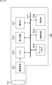
- FIG. 14 is a block diagram illustrating a configuration example of an imaging apparatus (camera apparatus) 1001 that is an example of an electronic apparatus to which the present technology is applied.
- the imaging device 1001 includes an optical system including a lens group 1011 and the like, an imaging element 1012, a DSP 1013 that is a camera signal processing unit, a frame memory 1014, a display device 1015, a recording device 1016, an operation system 1017, and And a power supply system 1018 and the like.
- a DSP 1013, a frame memory 1014, a display device 1015, a recording device 1016, an operation system 1017, and a power supply system 1018 are connected to each other via a bus line 1019.
- the lens group 1011 takes in incident light (image light) from a subject and forms an image on the imaging surface of the imaging element 1012.
- the imaging element 1012 converts the amount of incident light imaged on the imaging surface by the lens group 1011 into an electrical signal in units of pixels and outputs it as a pixel signal.
- the display device 1015 includes a panel display device such as a liquid crystal display device or an organic EL (electroluminescence) display device, and displays a moving image or a still image captured by the image sensor 1012.
- the recording device 1016 records a moving image or a still image captured by the image sensor 1012 on a recording medium such as a memory card, a video tape, or a DVD (Digital Versatile Disk).
- the operation system 1017 issues operation commands for various functions of the imaging apparatus 1001 under the operation of the user.
- the power supply system 1018 appropriately supplies various power supplies serving as operation power supplies for the DSP 1013, the frame memory 1014, the display device 1015, the recording device 1016, and the operation system 1017 to these supply targets.
- Such an imaging apparatus 1001 is applied to a camera module for a mobile device such as a video camera, a digital still camera, and a smartphone or a mobile phone.
- a camera module for a mobile device such as a video camera, a digital still camera, and a smartphone or a mobile phone.
- the imaging device according to each of the above-described embodiments can be used as the imaging element 1012. Thereby, the image quality of the imaging device 1001 can be improved.
- system represents the entire apparatus composed of a plurality of apparatuses.
- this technique can also take the following structures.
- a light receiving element array in which a plurality of light receiving elements made of a compound semiconductor having light receiving sensitivity in the infrared region are arranged;
- a signal processing circuit for processing a signal from the light receiving element;
- An upper electrode formed on the light receiving surface side of the light receiving element;
- a lower electrode paired with the upper electrode,
- the light receiving element array and the signal processing circuit are joined by a film of a predetermined material,
- the upper electrode and the signal processing circuit are connected via a through via penetrating a part of the light receiving element,
- the lower electrode is an electrode common to light receiving elements arranged in the light receiving element array.
- a light receiving element array in which a plurality of light receiving elements made of a compound semiconductor having light receiving sensitivity in the infrared region are arranged;
- a signal processing circuit for processing a signal from the light receiving element;
- An upper electrode formed on the light receiving surface side of the light receiving element;
- the manufacturing method including the step of forming the lower electrode as an electrode common to the light receiving elements arranged in the light receiving element array.
Landscapes
- Physics & Mathematics (AREA)
- Spectroscopy & Molecular Physics (AREA)
- General Physics & Mathematics (AREA)
- Engineering & Computer Science (AREA)
- Multimedia (AREA)
- Signal Processing (AREA)
- Manufacturing & Machinery (AREA)
- Solid State Image Pick-Up Elements (AREA)
- Transforming Light Signals Into Electric Signals (AREA)
Abstract
Description
1.画素の構成
2.受光層エリアの構成
3.製造について
4.撮像装置の使用例
本技術は、赤外線イメージセンサを備える撮像装置に適用できる。撮像装置としては、例えば、人や物などを検出する装置とすることができる。撮像装置は、図1に示すように受光層エリアに、画素アレイ部10を備える。画素アレイ部10には、複数の画素がアレイ状に配置されている。画素アレイ部10に配列されている画素は、赤外域に受光感度を持つ化合物半導体からなる受光素子である。
上記したように、上部電極49は、スルービア60により信号処理回路30内の配線32と接続され、下部電極50は、スルービア70により赤外線イメージセンサ40内の電極41と接続され、終端部分で信号処理回路30内の配線33と接続され、接地されている。または下部電極50’は、終端部分で赤外線イメージセンサ40内の電極41’と接続され、信号処理回路30内の配線33’と接続され、接地されている。
上記した画素20の製造について図7乃至図12を参照して説明する。
図13は、上述の撮像装置の使用例を示す図である。
・自動停止等の安全運転や、運転者の状態の認識等のために、自動車の前方や後方、周囲、車内等を撮影する車載用センサ、走行車両や道路を監視する監視カメラ、車両間等の測距を行う測距センサ等の、交通の用に供される装置
・ユーザのジェスチャを撮影して、そのジェスチャに従った機器操作を行うために、TVや、冷蔵庫、エアーコンディショナ等の家電に供される装置
・内視鏡や、赤外光の受光による血管撮影を行う装置等の、医療やヘルスケアの用に供される装置
・防犯用途の監視カメラや、人物認証用途のカメラ等の、セキュリティの用に供される装置
・肌を撮影する肌測定器や、頭皮を撮影するマイクロスコープ等の、美容の用に供され装置
・スポーツ用途等向けのアクションカメラやウェアラブルカメラ等の、スポーツの用に供される装置
・畑や作物の状態を監視するためのカメラ等の、農業の用に供される装置
(1)
赤外域に受光感度を持つ化合物半導体からなる受光素子が複数配列された受光素子アレイと、
前記受光素子からの信号を処理する信号処理回路と、
前記受光素子の受光面側に形成されている上部電極と、
前記上部電極と対をなす下部電極と
を備え、
前記受光素子アレイと前記信号処理回路は、所定の材料の膜で接合され、
前記受光素子の一部を貫通しているスルービアを介して、前記上部電極と前記信号処理回路は接続され、
前記下部電極は、前記受光素子アレイに配列された受光素子で共通した電極とされている
撮像装置。
(2)
前記化合物半導体は、III-V族半導体である
前記(1)に記載の撮像装置。
(3)
前記受光素子の下部に設けられた電極まで貫通しているスルービアを介して、前記下部電極と前記電極が接続されている
前記(1)または(2)に記載の撮像装置。
(4)
前記下部電極は、前記受光素子の下部に設けられた電極と、前記受光素子アレイの外周部で接続されている
前記(1)乃至(3)のいずれかに記載の撮像装置。
(5)
前記下部電極は、前記信号処理回路と、前記受光素子アレイの外周部で接続されている
前記(1)乃至(4)のいずれかに記載の撮像装置。
(6)
前記スルービアは、固定電荷膜で内部が覆われ、前記固定電荷膜上に、前記上部電極の一部が積層されている
前記(1)乃至(5)のいずれかに記載の撮像装置。
(7)
赤外域に受光感度を持つ化合物半導体からなる受光素子が複数配列された受光素子アレイと、
前記受光素子からの信号を処理する信号処理回路と、
前記受光素子の受光面側に形成されている上部電極と、
前記上部電極と対をなす下部電極と
を備える撮像装置を製造する製造方法において、
前記受光素子アレイと前記信号処理回路を、所定の材料の膜で接合し、
前記受光素子の一部を貫通するスルービアを形成し、
前記上部電極と前記信号処理回路を、前記スルービアを介して接続し、
前記下部電極を、前記受光素子アレイに配列された受光素子で共通した電極として形成する
ステップを含む製造方法。
(8)
前記化合物半導体は、III-V族半導体である
前記(7)に記載の製造方法。
(9)
前記受光素子の下部に電極を形成し、
前記受光素子の一部に、前記電極の上面まで貫通するスルービアを形成し、
前記下部電極と前記電極を前記スルービアを介して接続する
ステップをさらに含む
前記(7)または(8)に記載の製造方法。
(10)
前記下部電極を、前記受光素子の下部に設けられた電極と、前記受光素子アレイの外周部で接続するステップをさらに含む
前記(7)乃至(9)のいずれかに記載の製造方法。
(11)
前記下部電極を、前記信号処理回路と、前記受光素子アレイの外周部で接続するステップをさらに含む
前記(7)乃至(10)のいずれかに記載の製造方法。
Claims (11)
- 赤外域に受光感度を持つ化合物半導体からなる受光素子が複数配列された受光素子アレイと、
前記受光素子からの信号を処理する信号処理回路と、
前記受光素子の受光面側に形成されている上部電極と、
前記上部電極と対をなす下部電極と
を備え、
前記受光素子アレイと前記信号処理回路は、所定の材料の膜で接合され、
前記受光素子の一部を貫通しているスルービアを介して、前記上部電極と前記信号処理回路は接続され、
前記下部電極は、前記受光素子アレイに配列された受光素子で共通した電極とされている
撮像装置。 - 前記化合物半導体は、III-V族半導体である
請求項1に記載の撮像装置。 - 前記受光素子の下部に設けられた電極まで貫通しているスルービアを介して、前記下部電極と前記電極が接続されている
請求項1に記載の撮像装置。 - 前記下部電極は、前記受光素子の下部に設けられた電極と、前記受光素子アレイの外周部で接続されている
請求項1に記載の撮像装置。 - 前記下部電極は、前記信号処理回路と、前記受光素子アレイの外周部で接続されている
請求項1に記載の撮像装置。 - 前記スルービアは、固定電荷膜で内部が覆われ、前記固定電荷膜上に、前記上部電極の一部が積層されている
請求項1に記載の撮像装置。 - 赤外域に受光感度を持つ化合物半導体からなる受光素子が複数配列された受光素子アレイと、
前記受光素子からの信号を処理する信号処理回路と、
前記受光素子の受光面側に形成されている上部電極と、
前記上部電極と対をなす下部電極と
を備える撮像装置を製造する製造方法において、
前記受光素子アレイと前記信号処理回路を、所定の材料の膜で接合し、
前記受光素子の一部を貫通するスルービアを形成し、
前記上部電極と前記信号処理回路を、前記スルービアを介して接続し、
前記下部電極を、前記受光素子アレイに配列された受光素子で共通した電極として形成する
ステップを含む製造方法。 - 前記化合物半導体は、III-V族半導体である
請求項7に記載の製造方法。 - 前記受光素子の下部に電極を形成し、
前記受光素子の一部に、前記電極の上面まで貫通するスルービアを形成し、
前記下部電極と前記電極を前記スルービアを介して接続する
ステップをさらに含む
請求項7に記載の製造方法。 - 前記下部電極を、前記受光素子の下部に設けられた電極と、前記受光素子アレイの外周部で接続するステップをさらに含む
請求項7に記載の製造方法。 - 前記下部電極を、前記信号処理回路と、前記受光素子アレイの外周部で接続するステップをさらに含む
請求項7に記載の製造方法。
Priority Applications (3)
| Application Number | Priority Date | Filing Date | Title |
|---|---|---|---|
| US15/761,475 US10522582B2 (en) | 2015-10-05 | 2016-09-21 | Imaging apparatus |
| JP2017544444A JP6743035B2 (ja) | 2015-10-05 | 2016-09-21 | 撮像装置、製造方法 |
| US16/298,395 US10811456B2 (en) | 2015-10-05 | 2019-03-11 | Imaging apparatus and manufacturing method |
Applications Claiming Priority (2)
| Application Number | Priority Date | Filing Date | Title |
|---|---|---|---|
| JP2015197390 | 2015-10-05 | ||
| JP2015-197390 | 2015-10-05 |
Related Child Applications (2)
| Application Number | Title | Priority Date | Filing Date |
|---|---|---|---|
| US15/761,475 A-371-Of-International US10522582B2 (en) | 2015-10-05 | 2016-09-21 | Imaging apparatus |
| US16/298,395 Division US10811456B2 (en) | 2015-10-05 | 2019-03-11 | Imaging apparatus and manufacturing method |
Publications (1)
| Publication Number | Publication Date |
|---|---|
| WO2017061273A1 true WO2017061273A1 (ja) | 2017-04-13 |
Family
ID=58487566
Family Applications (1)
| Application Number | Title | Priority Date | Filing Date |
|---|---|---|---|
| PCT/JP2016/077789 Ceased WO2017061273A1 (ja) | 2015-10-05 | 2016-09-21 | 撮像装置、製造方法 |
Country Status (3)
| Country | Link |
|---|---|
| US (2) | US10522582B2 (ja) |
| JP (1) | JP6743035B2 (ja) |
| WO (1) | WO2017061273A1 (ja) |
Cited By (2)
| Publication number | Priority date | Publication date | Assignee | Title |
|---|---|---|---|---|
| JP2022538982A (ja) * | 2019-06-28 | 2022-09-07 | マサチューセッツ インスティテュート オブ テクノロジー | 光電子デバイス用集積構造体の製造方法及び光電子デバイス用集積構造体 |
| JP2023169866A (ja) * | 2022-05-17 | 2023-11-30 | 台湾積體電路製造股▲ふん▼有限公司 | 積層型cmosイメージセンサ及びその製造方法 |
Families Citing this family (11)
| Publication number | Priority date | Publication date | Assignee | Title |
|---|---|---|---|---|
| US12087871B2 (en) | 2013-05-22 | 2024-09-10 | W&W Sens Devices, Inc. | Microstructure enhanced absorption photosensitive devices |
| US11309444B1 (en) | 2015-11-20 | 2022-04-19 | W&W Sens Devices, Inc. | Microstructure enhanced absorption photosensitive devices |
| US11791432B2 (en) | 2013-05-22 | 2023-10-17 | W&Wsens Devices, Inc. | Microstructure enhanced absorption photosensitive devices |
| US12243948B2 (en) | 2013-05-22 | 2025-03-04 | W&W Sens Devices, Inc. | Microstructure enhanced absorption photosensitive devices |
| US10522582B2 (en) * | 2015-10-05 | 2019-12-31 | Sony Semiconductor Solutions Corporation | Imaging apparatus |
| WO2020189179A1 (ja) * | 2019-03-20 | 2020-09-24 | ソニーセミコンダクタソリューションズ株式会社 | 受光素子および受光素子の製造方法ならびに撮像装置 |
| JPWO2021009978A1 (ja) * | 2019-07-12 | 2021-01-21 | ||
| FR3100658A1 (fr) | 2019-09-10 | 2021-03-12 | Stmicroelectronics (Crolles 2) Sas | Dispositif électronique comprenant des composants optiques et électroniques intégrés et procédé de fabrication |
| US12094903B2 (en) | 2019-09-24 | 2024-09-17 | W&W Sens Devices, Inc | Microstructure enhanced absorption photosensitive devices |
| US12490540B2 (en) * | 2020-06-24 | 2025-12-02 | Dexerials Corporation | Optical semiconductor array |
| FR3118301B1 (fr) * | 2020-12-23 | 2022-12-30 | Thales Sa | Integration d'un circuit de detection a base de resonateurs optiques sur un circuit de lecture d'un imageur |
Citations (6)
| Publication number | Priority date | Publication date | Assignee | Title |
|---|---|---|---|---|
| JPH05218377A (ja) * | 1992-02-05 | 1993-08-27 | Mitsubishi Electric Corp | 半導体光検知器 |
| US5318666A (en) * | 1993-04-19 | 1994-06-07 | Texas Instruments Incorporated | Method for via formation and type conversion in group II and group VI materials |
| JP2012129247A (ja) * | 2010-12-13 | 2012-07-05 | Fujitsu Ltd | 赤外線撮像装置 |
| JP2014060380A (ja) * | 2012-06-14 | 2014-04-03 | Rohm Co Ltd | 光電変換装置 |
| JP2015149422A (ja) * | 2014-02-07 | 2015-08-20 | ソニー株式会社 | 受光素子、撮像素子及び撮像装置 |
| JP2015162679A (ja) * | 2014-02-27 | 2015-09-07 | 三星電子株式会社Samsung Electronics Co.,Ltd. | 負の電荷物質を含むトレンチを有するイメージセンサー及びその製造方法 |
Family Cites Families (33)
| Publication number | Priority date | Publication date | Assignee | Title |
|---|---|---|---|---|
| EP2234387B8 (en) * | 2009-03-24 | 2012-05-23 | Sony Corporation | Solid-state imaging device, driving method of solid-state imaging device, and electronic apparatus |
| JP2010251558A (ja) * | 2009-04-16 | 2010-11-04 | Toshiba Corp | 固体撮像装置 |
| JP2011009645A (ja) * | 2009-06-29 | 2011-01-13 | Toshiba Corp | 半導体装置及びその製造方法 |
| JP5442394B2 (ja) * | 2009-10-29 | 2014-03-12 | ソニー株式会社 | 固体撮像装置とその製造方法、及び電子機器 |
| JP5709435B2 (ja) * | 2010-08-23 | 2015-04-30 | キヤノン株式会社 | 撮像モジュール及びカメラ |
| JP2012084609A (ja) * | 2010-10-07 | 2012-04-26 | Sony Corp | 固体撮像装置とその製造方法、及び電子機器 |
| JP5640630B2 (ja) * | 2010-10-12 | 2014-12-17 | ソニー株式会社 | 固体撮像装置、固体撮像装置の製造方法、及び電子機器 |
| JP2012094720A (ja) * | 2010-10-27 | 2012-05-17 | Sony Corp | 固体撮像装置、半導体装置、固体撮像装置の製造方法、半導体装置の製造方法、及び電子機器 |
| US9595558B2 (en) * | 2013-11-12 | 2017-03-14 | Intrinsix Corporation | Photodiode architectures and image capture methods having a plurality of photodiode with a shared electrode |
| JP2012204501A (ja) * | 2011-03-24 | 2012-10-22 | Sony Corp | 半導体装置、電子デバイス、及び、半導体装置の製造方法 |
| US9153490B2 (en) * | 2011-07-19 | 2015-10-06 | Sony Corporation | Solid-state imaging device, manufacturing method of solid-state imaging device, manufacturing method of semiconductor device, semiconductor device, and electronic device |
| TWI577001B (zh) * | 2011-10-04 | 2017-04-01 | 新力股份有限公司 | 固體攝像裝置、固體攝像裝置之製造方法及電子機器 |
| CN103367374B (zh) * | 2012-04-02 | 2017-06-09 | 索尼公司 | 固体摄像装置及其制造方法、半导体器件的制造装置和方法、电子设备 |
| JP2014022448A (ja) * | 2012-07-13 | 2014-02-03 | Toshiba Corp | 固体撮像装置 |
| JP2014099582A (ja) * | 2012-10-18 | 2014-05-29 | Sony Corp | 固体撮像装置 |
| US10446700B2 (en) * | 2013-05-22 | 2019-10-15 | W&Wsens Devices, Inc. | Microstructure enhanced absorption photosensitive devices |
| JP6108172B2 (ja) * | 2013-09-02 | 2017-04-05 | ソニー株式会社 | 固体撮像素子およびその製造方法、並びに電子機器 |
| JP2015076502A (ja) * | 2013-10-09 | 2015-04-20 | ソニー株式会社 | 半導体装置およびその製造方法、並びに電子機器 |
| JP6291895B2 (ja) * | 2014-02-20 | 2018-03-14 | 富士通株式会社 | 赤外線検出器及びその製造方法 |
| JP6509596B2 (ja) * | 2014-03-18 | 2019-05-08 | 株式会社半導体エネルギー研究所 | 半導体装置 |
| JP2015179731A (ja) * | 2014-03-19 | 2015-10-08 | 株式会社東芝 | 固体撮像装置 |
| KR101581205B1 (ko) * | 2014-04-15 | 2015-12-31 | 주식회사 뷰웍스 | 광 검출기 |
| JP6424610B2 (ja) * | 2014-04-23 | 2018-11-21 | ソニー株式会社 | 半導体装置、および製造方法 |
| US9613994B2 (en) * | 2014-07-16 | 2017-04-04 | Taiwan Semiconductor Manufacturing Company, Ltd. | Capacitance device in a stacked scheme and methods of forming the same |
| US10180354B2 (en) * | 2014-11-07 | 2019-01-15 | Semiconductor Energy Laboratory Co., Ltd. | Imaging device and electronic device |
| CN107408565B (zh) * | 2015-03-03 | 2021-07-20 | 索尼公司 | 半导体装置和电子设备 |
| TWI692859B (zh) * | 2015-05-15 | 2020-05-01 | 日商新力股份有限公司 | 固體攝像裝置及其製造方法、以及電子機器 |
| JP6914001B2 (ja) * | 2015-08-12 | 2021-08-04 | 株式会社ソニー・インタラクティブエンタテインメント | 撮像素子、イメージセンサ、撮像装置、および情報処理装置 |
| US10522582B2 (en) * | 2015-10-05 | 2019-12-31 | Sony Semiconductor Solutions Corporation | Imaging apparatus |
| JP6701553B2 (ja) * | 2016-01-06 | 2020-05-27 | ローム株式会社 | 孔を有する基板およびその製造方法ならびに赤外線センサおよびその製造方法 |
| KR102605618B1 (ko) * | 2016-11-14 | 2023-11-23 | 삼성전자주식회사 | 이미지 센서 패키지 |
| JP2018081945A (ja) * | 2016-11-14 | 2018-05-24 | ソニーセミコンダクタソリューションズ株式会社 | 固体撮像素子および製造方法、並びに電子機器 |
| JP7116591B2 (ja) * | 2018-05-18 | 2022-08-10 | キヤノン株式会社 | 撮像装置及びその製造方法 |
-
2016
- 2016-09-21 US US15/761,475 patent/US10522582B2/en active Active
- 2016-09-21 JP JP2017544444A patent/JP6743035B2/ja not_active Expired - Fee Related
- 2016-09-21 WO PCT/JP2016/077789 patent/WO2017061273A1/ja not_active Ceased
-
2019
- 2019-03-11 US US16/298,395 patent/US10811456B2/en active Active
Patent Citations (6)
| Publication number | Priority date | Publication date | Assignee | Title |
|---|---|---|---|---|
| JPH05218377A (ja) * | 1992-02-05 | 1993-08-27 | Mitsubishi Electric Corp | 半導体光検知器 |
| US5318666A (en) * | 1993-04-19 | 1994-06-07 | Texas Instruments Incorporated | Method for via formation and type conversion in group II and group VI materials |
| JP2012129247A (ja) * | 2010-12-13 | 2012-07-05 | Fujitsu Ltd | 赤外線撮像装置 |
| JP2014060380A (ja) * | 2012-06-14 | 2014-04-03 | Rohm Co Ltd | 光電変換装置 |
| JP2015149422A (ja) * | 2014-02-07 | 2015-08-20 | ソニー株式会社 | 受光素子、撮像素子及び撮像装置 |
| JP2015162679A (ja) * | 2014-02-27 | 2015-09-07 | 三星電子株式会社Samsung Electronics Co.,Ltd. | 負の電荷物質を含むトレンチを有するイメージセンサー及びその製造方法 |
Cited By (5)
| Publication number | Priority date | Publication date | Assignee | Title |
|---|---|---|---|---|
| JP2022538982A (ja) * | 2019-06-28 | 2022-09-07 | マサチューセッツ インスティテュート オブ テクノロジー | 光電子デバイス用集積構造体の製造方法及び光電子デバイス用集積構造体 |
| JP7590074B2 (ja) | 2019-06-28 | 2024-11-26 | マサチューセッツ インスティテュート オブ テクノロジー | 光電子デバイス用集積構造体の製造方法及び光電子デバイス用集積構造体 |
| US12176461B2 (en) | 2019-06-28 | 2024-12-24 | Massachusetts Institute Of Technology | Method of fabricating an integrated structure for an optoelectronic device and integrated structure for an optoelectronic device |
| JP2023169866A (ja) * | 2022-05-17 | 2023-11-30 | 台湾積體電路製造股▲ふん▼有限公司 | 積層型cmosイメージセンサ及びその製造方法 |
| JP7804607B2 (ja) | 2022-05-17 | 2026-01-22 | 台湾積體電路製造股▲ふん▼有限公司 | 積層型cmosイメージセンサ及びその製造方法 |
Also Published As
| Publication number | Publication date |
|---|---|
| US10811456B2 (en) | 2020-10-20 |
| US20180261641A1 (en) | 2018-09-13 |
| JP6743035B2 (ja) | 2020-08-19 |
| US20190206921A1 (en) | 2019-07-04 |
| US10522582B2 (en) | 2019-12-31 |
| JPWO2017061273A1 (ja) | 2018-07-26 |
Similar Documents
| Publication | Publication Date | Title |
|---|---|---|
| JP6743035B2 (ja) | 撮像装置、製造方法 | |
| US11437423B2 (en) | Image sensor, manufacturing method, and electronic device | |
| JP6885331B2 (ja) | 半導体装置およびその製造方法、並びに電子機器 | |
| JP6879919B2 (ja) | 固体撮像素子、電子機器、及び、固体撮像素子の製造方法 | |
| CN107851607B (zh) | 固态图像传感器和电子设备 | |
| US20220328555A1 (en) | Solid-state imaging element and electronic device | |
| KR20230074836A (ko) | 촬상 소자 및 그 제조 방법 및 전자 기기 | |
| TWI800487B (zh) | 固體攝像元件及製造方法、以及電子機器 | |
| US20210408097A1 (en) | Solid-state imaging device and electronic device | |
| US11171170B2 (en) | Image sensor package with flexible printed circuits | |
| CN109478555B (zh) | 固体摄像元件、制造方法以及电子装置 | |
| JP2022016576A (ja) | 固体撮像素子、および電子装置 | |
| WO2017169881A1 (ja) | 半導体装置、半導体装置の製造方法、集積基板、及び、電子機器 | |
| US9865641B2 (en) | Solid-state imaging device, manufacturing method therefor, and imaging apparatus | |
| US10531020B2 (en) | Solid-state image pickup device, manufacturing method therefor, and electronic apparatus | |
| EP3518032B1 (en) | Camera module, manufacturing method, and electronic device | |
| US11948910B2 (en) | Manufacturing method of semiconductor apparatus and semiconductor apparatus | |
| US10867856B2 (en) | Semiconductor device and method of manufacturing the same, and electronic apparatus | |
| JP2017183387A (ja) | 回路基板、半導体装置、撮像装置、固体撮像素子、および固体撮像素子の製造方法、並びに電子機器 | |
| WO2024162013A1 (ja) | 固体撮像素子および製造方法、並びに電子機器 | |
| WO2023153300A1 (ja) | 固体撮像素子および製造方法、並びに電子機器 | |
| WO2020059237A1 (ja) | 固体撮像装置及び電子機器 |
Legal Events
| Date | Code | Title | Description |
|---|---|---|---|
| 121 | Ep: the epo has been informed by wipo that ep was designated in this application |
Ref document number: 16853427 Country of ref document: EP Kind code of ref document: A1 |
|
| ENP | Entry into the national phase |
Ref document number: 2017544444 Country of ref document: JP Kind code of ref document: A |
|
| WWE | Wipo information: entry into national phase |
Ref document number: 15761475 Country of ref document: US |
|
| NENP | Non-entry into the national phase |
Ref country code: DE |
|
| 122 | Ep: pct application non-entry in european phase |
Ref document number: 16853427 Country of ref document: EP Kind code of ref document: A1 |