JP6885331B2 - 半導体装置およびその製造方法、並びに電子機器 - Google Patents
半導体装置およびその製造方法、並びに電子機器 Download PDFInfo
- Publication number
- JP6885331B2 JP6885331B2 JP2017529550A JP2017529550A JP6885331B2 JP 6885331 B2 JP6885331 B2 JP 6885331B2 JP 2017529550 A JP2017529550 A JP 2017529550A JP 2017529550 A JP2017529550 A JP 2017529550A JP 6885331 B2 JP6885331 B2 JP 6885331B2
- Authority
- JP
- Japan
- Prior art keywords
- image sensor
- wiring layer
- glass substrate
- main surface
- semiconductor device
- Prior art date
- Legal status (The legal status is an assumption and is not a legal conclusion. Google has not performed a legal analysis and makes no representation as to the accuracy of the status listed.)
- Active
Links
Images


Classifications
-
- H—ELECTRICITY
- H10—SEMICONDUCTOR DEVICES; ELECTRIC SOLID-STATE DEVICES NOT OTHERWISE PROVIDED FOR
- H10F—INORGANIC SEMICONDUCTOR DEVICES SENSITIVE TO INFRARED RADIATION, LIGHT, ELECTROMAGNETIC RADIATION OF SHORTER WAVELENGTH OR CORPUSCULAR RADIATION
- H10F39/00—Integrated devices, or assemblies of multiple devices, comprising at least one element covered by group H10F30/00, e.g. radiation detectors comprising photodiode arrays
- H10F39/80—Constructional details of image sensors
- H10F39/804—Containers or encapsulations
-
- G—PHYSICS
- G02—OPTICS
- G02B—OPTICAL ELEMENTS, SYSTEMS OR APPARATUS
- G02B7/00—Mountings, adjusting means, or light-tight connections, for optical elements
- G02B7/02—Mountings, adjusting means, or light-tight connections, for optical elements for lenses
- G02B7/021—Mountings, adjusting means, or light-tight connections, for optical elements for lenses for more than one lens
-
- G—PHYSICS
- G02—OPTICS
- G02B—OPTICAL ELEMENTS, SYSTEMS OR APPARATUS
- G02B7/00—Mountings, adjusting means, or light-tight connections, for optical elements
- G02B7/02—Mountings, adjusting means, or light-tight connections, for optical elements for lenses
- G02B7/04—Mountings, adjusting means, or light-tight connections, for optical elements for lenses with mechanism for focusing or varying magnification
- G02B7/09—Mountings, adjusting means, or light-tight connections, for optical elements for lenses with mechanism for focusing or varying magnification adapted for automatic focusing or varying magnification
-
- H—ELECTRICITY
- H01—ELECTRIC ELEMENTS
- H01L—SEMICONDUCTOR DEVICES NOT COVERED BY CLASS H10
- H01L24/00—Arrangements for connecting or disconnecting semiconductor or solid-state bodies; Methods or apparatus related thereto
- H01L24/01—Means for bonding being attached to, or being formed on, the surface to be connected, e.g. chip-to-package, die-attach, "first-level" interconnects; Manufacturing methods related thereto
- H01L24/10—Bump connectors ; Manufacturing methods related thereto
- H01L24/12—Structure, shape, material or disposition of the bump connectors prior to the connecting process
- H01L24/14—Structure, shape, material or disposition of the bump connectors prior to the connecting process of a plurality of bump connectors
-
- H—ELECTRICITY
- H01—ELECTRIC ELEMENTS
- H01L—SEMICONDUCTOR DEVICES NOT COVERED BY CLASS H10
- H01L24/00—Arrangements for connecting or disconnecting semiconductor or solid-state bodies; Methods or apparatus related thereto
- H01L24/01—Means for bonding being attached to, or being formed on, the surface to be connected, e.g. chip-to-package, die-attach, "first-level" interconnects; Manufacturing methods related thereto
- H01L24/10—Bump connectors ; Manufacturing methods related thereto
- H01L24/15—Structure, shape, material or disposition of the bump connectors after the connecting process
- H01L24/17—Structure, shape, material or disposition of the bump connectors after the connecting process of a plurality of bump connectors
-
- H—ELECTRICITY
- H01—ELECTRIC ELEMENTS
- H01L—SEMICONDUCTOR DEVICES NOT COVERED BY CLASS H10
- H01L24/00—Arrangements for connecting or disconnecting semiconductor or solid-state bodies; Methods or apparatus related thereto
- H01L24/01—Means for bonding being attached to, or being formed on, the surface to be connected, e.g. chip-to-package, die-attach, "first-level" interconnects; Manufacturing methods related thereto
- H01L24/18—High density interconnect [HDI] connectors; Manufacturing methods related thereto
- H01L24/19—Manufacturing methods of high density interconnect preforms
-
- H—ELECTRICITY
- H01—ELECTRIC ELEMENTS
- H01L—SEMICONDUCTOR DEVICES NOT COVERED BY CLASS H10
- H01L24/00—Arrangements for connecting or disconnecting semiconductor or solid-state bodies; Methods or apparatus related thereto
- H01L24/73—Means for bonding being of different types provided for in two or more of groups H01L24/10, H01L24/18, H01L24/26, H01L24/34, H01L24/42, H01L24/50, H01L24/63, H01L24/71
-
- H—ELECTRICITY
- H01—ELECTRIC ELEMENTS
- H01L—SEMICONDUCTOR DEVICES NOT COVERED BY CLASS H10
- H01L24/00—Arrangements for connecting or disconnecting semiconductor or solid-state bodies; Methods or apparatus related thereto
- H01L24/91—Methods for connecting semiconductor or solid state bodies including different methods provided for in two or more of groups H01L24/80 - H01L24/90
- H01L24/92—Specific sequence of method steps
-
- H—ELECTRICITY
- H01—ELECTRIC ELEMENTS
- H01L—SEMICONDUCTOR DEVICES NOT COVERED BY CLASS H10
- H01L24/00—Arrangements for connecting or disconnecting semiconductor or solid-state bodies; Methods or apparatus related thereto
- H01L24/93—Batch processes
- H01L24/95—Batch processes at chip-level, i.e. with connecting carried out on a plurality of singulated devices, i.e. on diced chips
- H01L24/97—Batch processes at chip-level, i.e. with connecting carried out on a plurality of singulated devices, i.e. on diced chips the devices being connected to a common substrate, e.g. interposer, said common substrate being separable into individual assemblies after connecting
-
- H—ELECTRICITY
- H04—ELECTRIC COMMUNICATION TECHNIQUE
- H04N—PICTORIAL COMMUNICATION, e.g. TELEVISION
- H04N23/00—Cameras or camera modules comprising electronic image sensors; Control thereof
- H04N23/57—Mechanical or electrical details of cameras or camera modules specially adapted for being embedded in other devices
-
- H—ELECTRICITY
- H04—ELECTRIC COMMUNICATION TECHNIQUE
- H04N—PICTORIAL COMMUNICATION, e.g. TELEVISION
- H04N25/00—Circuitry of solid-state image sensors [SSIS]; Control thereof
-
- H—ELECTRICITY
- H10—SEMICONDUCTOR DEVICES; ELECTRIC SOLID-STATE DEVICES NOT OTHERWISE PROVIDED FOR
- H10F—INORGANIC SEMICONDUCTOR DEVICES SENSITIVE TO INFRARED RADIATION, LIGHT, ELECTROMAGNETIC RADIATION OF SHORTER WAVELENGTH OR CORPUSCULAR RADIATION
- H10F39/00—Integrated devices, or assemblies of multiple devices, comprising at least one element covered by group H10F30/00, e.g. radiation detectors comprising photodiode arrays
- H10F39/011—Manufacture or treatment of image sensors covered by group H10F39/12
-
- H—ELECTRICITY
- H10—SEMICONDUCTOR DEVICES; ELECTRIC SOLID-STATE DEVICES NOT OTHERWISE PROVIDED FOR
- H10F—INORGANIC SEMICONDUCTOR DEVICES SENSITIVE TO INFRARED RADIATION, LIGHT, ELECTROMAGNETIC RADIATION OF SHORTER WAVELENGTH OR CORPUSCULAR RADIATION
- H10F39/00—Integrated devices, or assemblies of multiple devices, comprising at least one element covered by group H10F30/00, e.g. radiation detectors comprising photodiode arrays
- H10F39/10—Integrated devices
- H10F39/12—Image sensors
- H10F39/18—Complementary metal-oxide-semiconductor [CMOS] image sensors; Photodiode array image sensors
- H10F39/182—Colour image sensors
-
- H—ELECTRICITY
- H10—SEMICONDUCTOR DEVICES; ELECTRIC SOLID-STATE DEVICES NOT OTHERWISE PROVIDED FOR
- H10F—INORGANIC SEMICONDUCTOR DEVICES SENSITIVE TO INFRARED RADIATION, LIGHT, ELECTROMAGNETIC RADIATION OF SHORTER WAVELENGTH OR CORPUSCULAR RADIATION
- H10F39/00—Integrated devices, or assemblies of multiple devices, comprising at least one element covered by group H10F30/00, e.g. radiation detectors comprising photodiode arrays
- H10F39/80—Constructional details of image sensors
- H10F39/805—Coatings
- H10F39/8053—Colour filters
-
- H—ELECTRICITY
- H10—SEMICONDUCTOR DEVICES; ELECTRIC SOLID-STATE DEVICES NOT OTHERWISE PROVIDED FOR
- H10F—INORGANIC SEMICONDUCTOR DEVICES SENSITIVE TO INFRARED RADIATION, LIGHT, ELECTROMAGNETIC RADIATION OF SHORTER WAVELENGTH OR CORPUSCULAR RADIATION
- H10F39/00—Integrated devices, or assemblies of multiple devices, comprising at least one element covered by group H10F30/00, e.g. radiation detectors comprising photodiode arrays
- H10F39/80—Constructional details of image sensors
- H10F39/805—Coatings
- H10F39/8057—Optical shielding
-
- H—ELECTRICITY
- H10—SEMICONDUCTOR DEVICES; ELECTRIC SOLID-STATE DEVICES NOT OTHERWISE PROVIDED FOR
- H10F—INORGANIC SEMICONDUCTOR DEVICES SENSITIVE TO INFRARED RADIATION, LIGHT, ELECTROMAGNETIC RADIATION OF SHORTER WAVELENGTH OR CORPUSCULAR RADIATION
- H10F39/00—Integrated devices, or assemblies of multiple devices, comprising at least one element covered by group H10F30/00, e.g. radiation detectors comprising photodiode arrays
- H10F39/80—Constructional details of image sensors
- H10F39/806—Optical elements or arrangements associated with the image sensors
- H10F39/8063—Microlenses
-
- H—ELECTRICITY
- H10—SEMICONDUCTOR DEVICES; ELECTRIC SOLID-STATE DEVICES NOT OTHERWISE PROVIDED FOR
- H10F—INORGANIC SEMICONDUCTOR DEVICES SENSITIVE TO INFRARED RADIATION, LIGHT, ELECTROMAGNETIC RADIATION OF SHORTER WAVELENGTH OR CORPUSCULAR RADIATION
- H10F39/00—Integrated devices, or assemblies of multiple devices, comprising at least one element covered by group H10F30/00, e.g. radiation detectors comprising photodiode arrays
- H10F39/80—Constructional details of image sensors
- H10F39/811—Interconnections
-
- H—ELECTRICITY
- H10—SEMICONDUCTOR DEVICES; ELECTRIC SOLID-STATE DEVICES NOT OTHERWISE PROVIDED FOR
- H10F—INORGANIC SEMICONDUCTOR DEVICES SENSITIVE TO INFRARED RADIATION, LIGHT, ELECTROMAGNETIC RADIATION OF SHORTER WAVELENGTH OR CORPUSCULAR RADIATION
- H10F99/00—Subject matter not provided for in other groups of this subclass
-
- G—PHYSICS
- G03—PHOTOGRAPHY; CINEMATOGRAPHY; ANALOGOUS TECHNIQUES USING WAVES OTHER THAN OPTICAL WAVES; ELECTROGRAPHY; HOLOGRAPHY
- G03B—APPARATUS OR ARRANGEMENTS FOR TAKING PHOTOGRAPHS OR FOR PROJECTING OR VIEWING THEM; APPARATUS OR ARRANGEMENTS EMPLOYING ANALOGOUS TECHNIQUES USING WAVES OTHER THAN OPTICAL WAVES; ACCESSORIES THEREFOR
- G03B13/00—Viewfinders; Focusing aids for cameras; Means for focusing for cameras; Autofocus systems for cameras
- G03B13/32—Means for focusing
- G03B13/34—Power focusing
- G03B13/36—Autofocus systems
-
- H—ELECTRICITY
- H01—ELECTRIC ELEMENTS
- H01L—SEMICONDUCTOR DEVICES NOT COVERED BY CLASS H10
- H01L2224/00—Indexing scheme for arrangements for connecting or disconnecting semiconductor or solid-state bodies and methods related thereto as covered by H01L24/00
- H01L2224/01—Means for bonding being attached to, or being formed on, the surface to be connected, e.g. chip-to-package, die-attach, "first-level" interconnects; Manufacturing methods related thereto
- H01L2224/02—Bonding areas; Manufacturing methods related thereto
- H01L2224/04—Structure, shape, material or disposition of the bonding areas prior to the connecting process
- H01L2224/04105—Bonding areas formed on an encapsulation of the semiconductor or solid-state body, e.g. bonding areas on chip-scale packages
-
- H—ELECTRICITY
- H01—ELECTRIC ELEMENTS
- H01L—SEMICONDUCTOR DEVICES NOT COVERED BY CLASS H10
- H01L2224/00—Indexing scheme for arrangements for connecting or disconnecting semiconductor or solid-state bodies and methods related thereto as covered by H01L24/00
- H01L2224/01—Means for bonding being attached to, or being formed on, the surface to be connected, e.g. chip-to-package, die-attach, "first-level" interconnects; Manufacturing methods related thereto
- H01L2224/10—Bump connectors; Manufacturing methods related thereto
- H01L2224/12—Structure, shape, material or disposition of the bump connectors prior to the connecting process
- H01L2224/12105—Bump connectors formed on an encapsulation of the semiconductor or solid-state body, e.g. bumps on chip-scale packages
-
- H—ELECTRICITY
- H01—ELECTRIC ELEMENTS
- H01L—SEMICONDUCTOR DEVICES NOT COVERED BY CLASS H10
- H01L2224/00—Indexing scheme for arrangements for connecting or disconnecting semiconductor or solid-state bodies and methods related thereto as covered by H01L24/00
- H01L2224/01—Means for bonding being attached to, or being formed on, the surface to be connected, e.g. chip-to-package, die-attach, "first-level" interconnects; Manufacturing methods related thereto
- H01L2224/10—Bump connectors; Manufacturing methods related thereto
- H01L2224/12—Structure, shape, material or disposition of the bump connectors prior to the connecting process
- H01L2224/13—Structure, shape, material or disposition of the bump connectors prior to the connecting process of an individual bump connector
- H01L2224/13001—Core members of the bump connector
- H01L2224/13099—Material
- H01L2224/131—Material with a principal constituent of the material being a metal or a metalloid, e.g. boron [B], silicon [Si], germanium [Ge], arsenic [As], antimony [Sb], tellurium [Te] and polonium [Po], and alloys thereof
-
- H—ELECTRICITY
- H01—ELECTRIC ELEMENTS
- H01L—SEMICONDUCTOR DEVICES NOT COVERED BY CLASS H10
- H01L2224/00—Indexing scheme for arrangements for connecting or disconnecting semiconductor or solid-state bodies and methods related thereto as covered by H01L24/00
- H01L2224/01—Means for bonding being attached to, or being formed on, the surface to be connected, e.g. chip-to-package, die-attach, "first-level" interconnects; Manufacturing methods related thereto
- H01L2224/10—Bump connectors; Manufacturing methods related thereto
- H01L2224/12—Structure, shape, material or disposition of the bump connectors prior to the connecting process
- H01L2224/14—Structure, shape, material or disposition of the bump connectors prior to the connecting process of a plurality of bump connectors
- H01L2224/141—Disposition
- H01L2224/1412—Layout
- H01L2224/1413—Square or rectangular array
- H01L2224/14134—Square or rectangular array covering only portions of the surface to be connected
- H01L2224/14135—Covering only the peripheral area of the surface to be connected, i.e. peripheral arrangements
-
- H—ELECTRICITY
- H01—ELECTRIC ELEMENTS
- H01L—SEMICONDUCTOR DEVICES NOT COVERED BY CLASS H10
- H01L2224/00—Indexing scheme for arrangements for connecting or disconnecting semiconductor or solid-state bodies and methods related thereto as covered by H01L24/00
- H01L2224/01—Means for bonding being attached to, or being formed on, the surface to be connected, e.g. chip-to-package, die-attach, "first-level" interconnects; Manufacturing methods related thereto
- H01L2224/10—Bump connectors; Manufacturing methods related thereto
- H01L2224/12—Structure, shape, material or disposition of the bump connectors prior to the connecting process
- H01L2224/14—Structure, shape, material or disposition of the bump connectors prior to the connecting process of a plurality of bump connectors
- H01L2224/141—Disposition
- H01L2224/1418—Disposition being disposed on at least two different sides of the body, e.g. dual array
- H01L2224/14181—On opposite sides of the body
-
- H—ELECTRICITY
- H01—ELECTRIC ELEMENTS
- H01L—SEMICONDUCTOR DEVICES NOT COVERED BY CLASS H10
- H01L2224/00—Indexing scheme for arrangements for connecting or disconnecting semiconductor or solid-state bodies and methods related thereto as covered by H01L24/00
- H01L2224/01—Means for bonding being attached to, or being formed on, the surface to be connected, e.g. chip-to-package, die-attach, "first-level" interconnects; Manufacturing methods related thereto
- H01L2224/10—Bump connectors; Manufacturing methods related thereto
- H01L2224/15—Structure, shape, material or disposition of the bump connectors after the connecting process
- H01L2224/16—Structure, shape, material or disposition of the bump connectors after the connecting process of an individual bump connector
- H01L2224/161—Disposition
- H01L2224/16151—Disposition the bump connector connecting between a semiconductor or solid-state body and an item not being a semiconductor or solid-state body, e.g. chip-to-substrate, chip-to-passive
- H01L2224/16221—Disposition the bump connector connecting between a semiconductor or solid-state body and an item not being a semiconductor or solid-state body, e.g. chip-to-substrate, chip-to-passive the body and the item being stacked
- H01L2224/16225—Disposition the bump connector connecting between a semiconductor or solid-state body and an item not being a semiconductor or solid-state body, e.g. chip-to-substrate, chip-to-passive the body and the item being stacked the item being non-metallic, e.g. insulating substrate with or without metallisation
- H01L2224/16227—Disposition the bump connector connecting between a semiconductor or solid-state body and an item not being a semiconductor or solid-state body, e.g. chip-to-substrate, chip-to-passive the body and the item being stacked the item being non-metallic, e.g. insulating substrate with or without metallisation the bump connector connecting to a bond pad of the item
-
- H—ELECTRICITY
- H01—ELECTRIC ELEMENTS
- H01L—SEMICONDUCTOR DEVICES NOT COVERED BY CLASS H10
- H01L2224/00—Indexing scheme for arrangements for connecting or disconnecting semiconductor or solid-state bodies and methods related thereto as covered by H01L24/00
- H01L2224/73—Means for bonding being of different types provided for in two or more of groups H01L2224/10, H01L2224/18, H01L2224/26, H01L2224/34, H01L2224/42, H01L2224/50, H01L2224/63, H01L2224/71
- H01L2224/732—Location after the connecting process
- H01L2224/73201—Location after the connecting process on the same surface
- H01L2224/73203—Bump and layer connectors
- H01L2224/73204—Bump and layer connectors the bump connector being embedded into the layer connector
-
- H—ELECTRICITY
- H01—ELECTRIC ELEMENTS
- H01L—SEMICONDUCTOR DEVICES NOT COVERED BY CLASS H10
- H01L2224/00—Indexing scheme for arrangements for connecting or disconnecting semiconductor or solid-state bodies and methods related thereto as covered by H01L24/00
- H01L2224/73—Means for bonding being of different types provided for in two or more of groups H01L2224/10, H01L2224/18, H01L2224/26, H01L2224/34, H01L2224/42, H01L2224/50, H01L2224/63, H01L2224/71
- H01L2224/732—Location after the connecting process
- H01L2224/73251—Location after the connecting process on different surfaces
- H01L2224/73253—Bump and layer connectors
-
- H—ELECTRICITY
- H01—ELECTRIC ELEMENTS
- H01L—SEMICONDUCTOR DEVICES NOT COVERED BY CLASS H10
- H01L2224/00—Indexing scheme for arrangements for connecting or disconnecting semiconductor or solid-state bodies and methods related thereto as covered by H01L24/00
- H01L2224/73—Means for bonding being of different types provided for in two or more of groups H01L2224/10, H01L2224/18, H01L2224/26, H01L2224/34, H01L2224/42, H01L2224/50, H01L2224/63, H01L2224/71
- H01L2224/732—Location after the connecting process
- H01L2224/73251—Location after the connecting process on different surfaces
- H01L2224/73259—Bump and HDI connectors
-
- H—ELECTRICITY
- H01—ELECTRIC ELEMENTS
- H01L—SEMICONDUCTOR DEVICES NOT COVERED BY CLASS H10
- H01L2224/00—Indexing scheme for arrangements for connecting or disconnecting semiconductor or solid-state bodies and methods related thereto as covered by H01L24/00
- H01L2224/73—Means for bonding being of different types provided for in two or more of groups H01L2224/10, H01L2224/18, H01L2224/26, H01L2224/34, H01L2224/42, H01L2224/50, H01L2224/63, H01L2224/71
- H01L2224/732—Location after the connecting process
- H01L2224/73251—Location after the connecting process on different surfaces
- H01L2224/73267—Layer and HDI connectors
-
- H—ELECTRICITY
- H01—ELECTRIC ELEMENTS
- H01L—SEMICONDUCTOR DEVICES NOT COVERED BY CLASS H10
- H01L2224/00—Indexing scheme for arrangements for connecting or disconnecting semiconductor or solid-state bodies and methods related thereto as covered by H01L24/00
- H01L2224/80—Methods for connecting semiconductor or other solid state bodies using means for bonding being attached to, or being formed on, the surface to be connected
- H01L2224/81—Methods for connecting semiconductor or other solid state bodies using means for bonding being attached to, or being formed on, the surface to be connected using a bump connector
- H01L2224/81001—Methods for connecting semiconductor or other solid state bodies using means for bonding being attached to, or being formed on, the surface to be connected using a bump connector involving a temporary auxiliary member not forming part of the bonding apparatus
- H01L2224/81005—Methods for connecting semiconductor or other solid state bodies using means for bonding being attached to, or being formed on, the surface to be connected using a bump connector involving a temporary auxiliary member not forming part of the bonding apparatus being a temporary or sacrificial substrate
-
- H—ELECTRICITY
- H01—ELECTRIC ELEMENTS
- H01L—SEMICONDUCTOR DEVICES NOT COVERED BY CLASS H10
- H01L2224/00—Indexing scheme for arrangements for connecting or disconnecting semiconductor or solid-state bodies and methods related thereto as covered by H01L24/00
- H01L2224/80—Methods for connecting semiconductor or other solid state bodies using means for bonding being attached to, or being formed on, the surface to be connected
- H01L2224/81—Methods for connecting semiconductor or other solid state bodies using means for bonding being attached to, or being formed on, the surface to be connected using a bump connector
- H01L2224/8119—Arrangement of the bump connectors prior to mounting
- H01L2224/81191—Arrangement of the bump connectors prior to mounting wherein the bump connectors are disposed only on the semiconductor or solid-state body
-
- H—ELECTRICITY
- H01—ELECTRIC ELEMENTS
- H01L—SEMICONDUCTOR DEVICES NOT COVERED BY CLASS H10
- H01L2224/00—Indexing scheme for arrangements for connecting or disconnecting semiconductor or solid-state bodies and methods related thereto as covered by H01L24/00
- H01L2224/80—Methods for connecting semiconductor or other solid state bodies using means for bonding being attached to, or being formed on, the surface to be connected
- H01L2224/81—Methods for connecting semiconductor or other solid state bodies using means for bonding being attached to, or being formed on, the surface to be connected using a bump connector
- H01L2224/81909—Post-treatment of the bump connector or bonding area
- H01L2224/81951—Forming additional members, e.g. for reinforcing
-
- H—ELECTRICITY
- H01—ELECTRIC ELEMENTS
- H01L—SEMICONDUCTOR DEVICES NOT COVERED BY CLASS H10
- H01L2224/00—Indexing scheme for arrangements for connecting or disconnecting semiconductor or solid-state bodies and methods related thereto as covered by H01L24/00
- H01L2224/80—Methods for connecting semiconductor or other solid state bodies using means for bonding being attached to, or being formed on, the surface to be connected
- H01L2224/83—Methods for connecting semiconductor or other solid state bodies using means for bonding being attached to, or being formed on, the surface to be connected using a layer connector
- H01L2224/8319—Arrangement of the layer connectors prior to mounting
- H01L2224/83192—Arrangement of the layer connectors prior to mounting wherein the layer connectors are disposed only on another item or body to be connected to the semiconductor or solid-state body
-
- H—ELECTRICITY
- H01—ELECTRIC ELEMENTS
- H01L—SEMICONDUCTOR DEVICES NOT COVERED BY CLASS H10
- H01L2224/00—Indexing scheme for arrangements for connecting or disconnecting semiconductor or solid-state bodies and methods related thereto as covered by H01L24/00
- H01L2224/91—Methods for connecting semiconductor or solid state bodies including different methods provided for in two or more of groups H01L2224/80 - H01L2224/90
- H01L2224/92—Specific sequence of method steps
- H01L2224/922—Connecting different surfaces of the semiconductor or solid-state body with connectors of different types
- H01L2224/9222—Sequential connecting processes
- H01L2224/92222—Sequential connecting processes the first connecting process involving a bump connector
- H01L2224/92224—Sequential connecting processes the first connecting process involving a bump connector the second connecting process involving a build-up interconnect
-
- H—ELECTRICITY
- H01—ELECTRIC ELEMENTS
- H01L—SEMICONDUCTOR DEVICES NOT COVERED BY CLASS H10
- H01L2224/00—Indexing scheme for arrangements for connecting or disconnecting semiconductor or solid-state bodies and methods related thereto as covered by H01L24/00
- H01L2224/91—Methods for connecting semiconductor or solid state bodies including different methods provided for in two or more of groups H01L2224/80 - H01L2224/90
- H01L2224/92—Specific sequence of method steps
- H01L2224/922—Connecting different surfaces of the semiconductor or solid-state body with connectors of different types
- H01L2224/9222—Sequential connecting processes
- H01L2224/92222—Sequential connecting processes the first connecting process involving a bump connector
- H01L2224/92225—Sequential connecting processes the first connecting process involving a bump connector the second connecting process involving a layer connector
-
- H—ELECTRICITY
- H01—ELECTRIC ELEMENTS
- H01L—SEMICONDUCTOR DEVICES NOT COVERED BY CLASS H10
- H01L2224/00—Indexing scheme for arrangements for connecting or disconnecting semiconductor or solid-state bodies and methods related thereto as covered by H01L24/00
- H01L2224/91—Methods for connecting semiconductor or solid state bodies including different methods provided for in two or more of groups H01L2224/80 - H01L2224/90
- H01L2224/92—Specific sequence of method steps
- H01L2224/922—Connecting different surfaces of the semiconductor or solid-state body with connectors of different types
- H01L2224/9222—Sequential connecting processes
- H01L2224/92242—Sequential connecting processes the first connecting process involving a layer connector
- H01L2224/92244—Sequential connecting processes the first connecting process involving a layer connector the second connecting process involving a build-up interconnect
-
- H—ELECTRICITY
- H01—ELECTRIC ELEMENTS
- H01L—SEMICONDUCTOR DEVICES NOT COVERED BY CLASS H10
- H01L2224/00—Indexing scheme for arrangements for connecting or disconnecting semiconductor or solid-state bodies and methods related thereto as covered by H01L24/00
- H01L2224/93—Batch processes
- H01L2224/95—Batch processes at chip-level, i.e. with connecting carried out on a plurality of singulated devices, i.e. on diced chips
- H01L2224/95001—Batch processes at chip-level, i.e. with connecting carried out on a plurality of singulated devices, i.e. on diced chips involving a temporary auxiliary member not forming part of the bonding apparatus, e.g. removable or sacrificial coating, film or substrate
-
- H—ELECTRICITY
- H01—ELECTRIC ELEMENTS
- H01L—SEMICONDUCTOR DEVICES NOT COVERED BY CLASS H10
- H01L2224/00—Indexing scheme for arrangements for connecting or disconnecting semiconductor or solid-state bodies and methods related thereto as covered by H01L24/00
- H01L2224/93—Batch processes
- H01L2224/95—Batch processes at chip-level, i.e. with connecting carried out on a plurality of singulated devices, i.e. on diced chips
- H01L2224/97—Batch processes at chip-level, i.e. with connecting carried out on a plurality of singulated devices, i.e. on diced chips the devices being connected to a common substrate, e.g. interposer, said common substrate being separable into individual assemblies after connecting
-
- H—ELECTRICITY
- H01—ELECTRIC ELEMENTS
- H01L—SEMICONDUCTOR DEVICES NOT COVERED BY CLASS H10
- H01L24/00—Arrangements for connecting or disconnecting semiconductor or solid-state bodies; Methods or apparatus related thereto
- H01L24/01—Means for bonding being attached to, or being formed on, the surface to be connected, e.g. chip-to-package, die-attach, "first-level" interconnects; Manufacturing methods related thereto
- H01L24/10—Bump connectors ; Manufacturing methods related thereto
- H01L24/12—Structure, shape, material or disposition of the bump connectors prior to the connecting process
- H01L24/13—Structure, shape, material or disposition of the bump connectors prior to the connecting process of an individual bump connector
-
- H—ELECTRICITY
- H01—ELECTRIC ELEMENTS
- H01L—SEMICONDUCTOR DEVICES NOT COVERED BY CLASS H10
- H01L24/00—Arrangements for connecting or disconnecting semiconductor or solid-state bodies; Methods or apparatus related thereto
- H01L24/01—Means for bonding being attached to, or being formed on, the surface to be connected, e.g. chip-to-package, die-attach, "first-level" interconnects; Manufacturing methods related thereto
- H01L24/10—Bump connectors ; Manufacturing methods related thereto
- H01L24/15—Structure, shape, material or disposition of the bump connectors after the connecting process
- H01L24/16—Structure, shape, material or disposition of the bump connectors after the connecting process of an individual bump connector
-
- H—ELECTRICITY
- H01—ELECTRIC ELEMENTS
- H01L—SEMICONDUCTOR DEVICES NOT COVERED BY CLASS H10
- H01L24/00—Arrangements for connecting or disconnecting semiconductor or solid-state bodies; Methods or apparatus related thereto
- H01L24/80—Methods for connecting semiconductor or other solid state bodies using means for bonding being attached to, or being formed on, the surface to be connected
- H01L24/81—Methods for connecting semiconductor or other solid state bodies using means for bonding being attached to, or being formed on, the surface to be connected using a bump connector
-
- H—ELECTRICITY
- H01—ELECTRIC ELEMENTS
- H01L—SEMICONDUCTOR DEVICES NOT COVERED BY CLASS H10
- H01L24/00—Arrangements for connecting or disconnecting semiconductor or solid-state bodies; Methods or apparatus related thereto
- H01L24/80—Methods for connecting semiconductor or other solid state bodies using means for bonding being attached to, or being formed on, the surface to be connected
- H01L24/83—Methods for connecting semiconductor or other solid state bodies using means for bonding being attached to, or being formed on, the surface to be connected using a layer connector
-
- H—ELECTRICITY
- H01—ELECTRIC ELEMENTS
- H01L—SEMICONDUCTOR DEVICES NOT COVERED BY CLASS H10
- H01L24/00—Arrangements for connecting or disconnecting semiconductor or solid-state bodies; Methods or apparatus related thereto
- H01L24/93—Batch processes
- H01L24/95—Batch processes at chip-level, i.e. with connecting carried out on a plurality of singulated devices, i.e. on diced chips
- H01L24/96—Batch processes at chip-level, i.e. with connecting carried out on a plurality of singulated devices, i.e. on diced chips the devices being encapsulated in a common layer, e.g. neo-wafer or pseudo-wafer, said common layer being separable into individual assemblies after connecting
-
- H—ELECTRICITY
- H01—ELECTRIC ELEMENTS
- H01L—SEMICONDUCTOR DEVICES NOT COVERED BY CLASS H10
- H01L2924/00—Indexing scheme for arrangements or methods for connecting or disconnecting semiconductor or solid-state bodies as covered by H01L24/00
- H01L2924/15—Details of package parts other than the semiconductor or other solid state devices to be connected
- H01L2924/151—Die mounting substrate
- H01L2924/1515—Shape
- H01L2924/15151—Shape the die mounting substrate comprising an aperture, e.g. for underfilling, outgassing, window type wire connections
-
- H—ELECTRICITY
- H01—ELECTRIC ELEMENTS
- H01L—SEMICONDUCTOR DEVICES NOT COVERED BY CLASS H10
- H01L2924/00—Indexing scheme for arrangements or methods for connecting or disconnecting semiconductor or solid-state bodies as covered by H01L24/00
- H01L2924/15—Details of package parts other than the semiconductor or other solid state devices to be connected
- H01L2924/151—Die mounting substrate
- H01L2924/1515—Shape
- H01L2924/15153—Shape the die mounting substrate comprising a recess for hosting the device
-
- H—ELECTRICITY
- H01—ELECTRIC ELEMENTS
- H01L—SEMICONDUCTOR DEVICES NOT COVERED BY CLASS H10
- H01L2924/00—Indexing scheme for arrangements or methods for connecting or disconnecting semiconductor or solid-state bodies as covered by H01L24/00
- H01L2924/15—Details of package parts other than the semiconductor or other solid state devices to be connected
- H01L2924/151—Die mounting substrate
- H01L2924/153—Connection portion
- H01L2924/1531—Connection portion the connection portion being formed only on the surface of the substrate opposite to the die mounting surface
- H01L2924/15311—Connection portion the connection portion being formed only on the surface of the substrate opposite to the die mounting surface being a ball array, e.g. BGA
-
- H—ELECTRICITY
- H01—ELECTRIC ELEMENTS
- H01L—SEMICONDUCTOR DEVICES NOT COVERED BY CLASS H10
- H01L2924/00—Indexing scheme for arrangements or methods for connecting or disconnecting semiconductor or solid-state bodies as covered by H01L24/00
- H01L2924/15—Details of package parts other than the semiconductor or other solid state devices to be connected
- H01L2924/151—Die mounting substrate
- H01L2924/153—Connection portion
- H01L2924/1532—Connection portion the connection portion being formed on the die mounting surface of the substrate
- H01L2924/15321—Connection portion the connection portion being formed on the die mounting surface of the substrate being a ball array, e.g. BGA
-
- H—ELECTRICITY
- H01—ELECTRIC ELEMENTS
- H01L—SEMICONDUCTOR DEVICES NOT COVERED BY CLASS H10
- H01L2924/00—Indexing scheme for arrangements or methods for connecting or disconnecting semiconductor or solid-state bodies as covered by H01L24/00
- H01L2924/15—Details of package parts other than the semiconductor or other solid state devices to be connected
- H01L2924/161—Cap
- H01L2924/1615—Shape
- H01L2924/16195—Flat cap [not enclosing an internal cavity]
Landscapes
- Engineering & Computer Science (AREA)
- Computer Hardware Design (AREA)
- Power Engineering (AREA)
- Microelectronics & Electronic Packaging (AREA)
- Physics & Mathematics (AREA)
- Optics & Photonics (AREA)
- General Physics & Mathematics (AREA)
- Signal Processing (AREA)
- Multimedia (AREA)
- Manufacturing & Machinery (AREA)
- Solid State Image Pick-Up Elements (AREA)
- Transforming Light Signals Into Electric Signals (AREA)
- Electromagnetism (AREA)
Description
1.イメージセンサパッケージの第1の実施の形態
2.イメージセンサパッケージの第2の実施の形態
3.イメージセンサパッケージの第3の実施の形態
4.イメージセンサパッケージの第4の実施の形態
5.イメージセンサパッケージの第5の実施の形態
6.イメージセンサパッケージの第6の実施の形態
7.イメージセンサパッケージの第7の実施の形態
8.イメージセンサパッケージの第8の実施の形態
9.マルチチップモジュール構成例
10.カメラモジュール構成例
11.複眼カメラモジュール構成例
12.電子機器への適用例
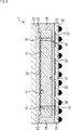
<1.1 第1の実施の形態の構造図>
図1は、本技術を適用した半導体装置の第1の実施の形態としての、イメージセンサパッケージの断面図を示している。
次に、図3を参照して、第1の実施の形態のイメージセンサパッケージ1の製造方法(第1の製造方法)について説明する。
図4は、第1の実施の形態の第1変形例を示すイメージセンサパッケージ1の断面図である。
図5は、第1の実施の形態の第2変形例を示すイメージセンサパッケージ1の断面図である。
<2.1 第2の実施の形態の構造図>
図6は、本技術を適用した半導体装置の第2の実施の形態としての、イメージセンサパッケージの断面図を示している。
次に、図7を参照して、第2の実施の形態のイメージセンサパッケージ1の製造方法(第2の製造方法)について説明する。
<3.1 第3の実施の形態の構造図>
図8は、本技術を適用した半導体装置の第3の実施の形態としての、イメージセンサパッケージの断面図を示している。
次に、図9を参照して、第3の実施の形態のイメージセンサパッケージ1の製造方法(第3の製造方法)について説明する。
<4.1 第4の実施の形態の構造図>
図10は、本技術を適用した半導体装置の第4の実施の形態としての、イメージセンサパッケージの断面図を示している。
次に、図12を参照して、第4の実施の形態のイメージセンサパッケージ1の製造方法(第4の製造方法)について説明する。
図13は、第4の実施の形態の第1変形例を示すイメージセンサパッケージ1の断面図である。
図14は、第4の実施の形態の第2変形例を示すイメージセンサパッケージ1の断面図である。
図16は、第4の実施の形態の第3変形例を示すイメージセンサパッケージ1の断面図である。
<5.1 第5の実施の形態の構造図>
図17は、本技術を適用した半導体装置の第5の実施の形態としての、イメージセンサパッケージの断面図を示している。
次に、図18を参照して、第5の実施の形態のイメージセンサパッケージ1の製造方法(第5の製造方法)について説明する。
<6.1 第6の実施の形態の構造図>
図19は、本技術を適用した半導体装置の第6の実施の形態としての、イメージセンサパッケージの断面図を示している。
次に、図20を参照して、第6の実施の形態のイメージセンサパッケージ1の製造方法(第6の製造方法)について説明する。
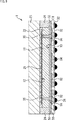
図20のFに示したガラス基板23の薄化の工程では、ガラス基板23が、イメージセンサ11ごとに分断されるまで薄化するようにしたが、完全に分断されるまで薄化しなくてもよい。
<7.1 第7の実施の形態の構造図>
図22は、本技術を適用した半導体装置の第7の実施の形態としての、イメージセンサパッケージの断面図を示している。
次に、図23を参照して、第7の実施の形態のイメージセンサパッケージ1の製造方法(第7の製造方法)について説明する。
<8.1 第8の実施の形態の構造図>
図24は、本技術を適用した半導体装置の第8の実施の形態としての、イメージセンサパッケージの断面図を示している。
次に、図25を参照して、第8の実施の形態のイメージセンサパッケージ1の製造方法(第8の製造方法)について説明する。
図25のDに示したガラス基板23の薄化の工程では、ガラス基板23が、イメージセンサ11ごとに分断されるまで薄化するようにしたが、完全に分断されるまで薄化しなくてもよい。この場合、溝部91においても、所定の厚みでガラス基板23が残ることになり、図26に示されるような、ガラス基板23の端部において、板厚が、イメージセンサ11上方よりも薄く形成されたイメージセンサパッケージ1を製造することができる。
図27は、第8の実施の形態の第2変形例を示すイメージセンサパッケージ1の断面図である。
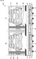
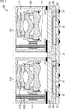
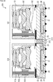
図28は、イメージセンサパッケージ1が、構成部品として、抵抗、キャパシタ、トランジスタ等のチップ部品をさらに含み、マルチチップモジュール構造としたイメージセンサパッケージの構成例を示している。
図29は、上述した各実施の形態のイメージセンサパッケージにレンズ構造体を組み立てたカメラモジュールの構成例を示している。
次に、複眼カメラモジュールの構成例について説明する。
図30は、複眼カメラモジュールの第1構成例を示している。
図31は、複眼カメラモジュールの第2構成例を示している。
図32は、複眼カメラモジュールの第3構成例を示している。
図33は、複眼カメラモジュールの第4構成例を示している。
図34は、複眼カメラモジュールの第5構成例を示している。
上述したイメージセンサパッケージ1、カメラモジュール151、または複眼カメラモジュール201は、デジタルスチルカメラやビデオカメラ等の撮像装置や、撮像機能を有する携帯端末装置や、画像読取部に固体撮像装置を用いる複写機など、画像取込部(光電変換部)に固体撮像装置を用いる電子機器に組み込んだ形で使用することが可能である。
図37は、イメージセンサパッケージ1、カメラモジュール151、または複眼カメラモジュール201として構成されたイメージセンサの使用例を示す図である。
・自動停止等の安全運転や、運転者の状態の認識等のために、自動車の前方や後方、周囲、車内等を撮影する車載用センサ、走行車両や道路を監視する監視カメラ、車両間等の測距を行う測距センサ等の、交通の用に供される装置
・ユーザのジェスチャを撮影して、そのジェスチャに従った機器操作を行うために、TVや、冷蔵庫、エアーコンディショナ等の家電に供される装置
・内視鏡や、赤外光の受光による血管撮影を行う装置等の、医療やヘルスケアの用に供される装置
・防犯用途の監視カメラや、人物認証用途のカメラ等の、セキュリティの用に供される装置
・肌を撮影する肌測定器や、頭皮を撮影するマイクロスコープ等の、美容の用に供される装置
・スポーツ用途等向けのアクションカメラやウェアラブルカメラ等の、スポーツの用に供される装置
・畑や作物の状態を監視するためのカメラ等の、農業の用に供される装置
(1)
半導体基板に光電変換素子が形成されたイメージセンサと、
前記イメージセンサの第1の主面側に配置されたガラス基板と、
前記イメージセンサの前記第1の主面と反対側の第2の主面側に形成された第1配線層と、
前記イメージセンサの信号を外部に出力する外部端子と
を備え、
前記第1配線層の金属配線は、前記イメージセンサの内部から外周部へ拡がるように形成されて前記外部端子と接続されている
半導体装置。
(2)
半導体基板に光電変換素子が形成されたイメージセンサと、
前記イメージセンサの受光面である第1の主面を保護するガラス基板と、
前記イメージセンサと前記ガラス基板の側面を覆う絶縁性部材と
を備える半導体装置。
(3)
前記第1配線層が形成されている平面領域は、前記イメージセンサの平面領域よりも大きい
前記(1)または(2)に記載の半導体装置。
(4)
前記ガラス基板と前記第1配線層との間であって、前記イメージセンサの側面は、絶縁性材料で覆われている
前記(1)乃至(3)のいずれかに記載の半導体装置。
(5)
前記絶縁性材料は、遮光性の材料と高熱伝導性を有する材料の2種類の絶縁性材料を含む
前記(4)に記載の半導体装置。
(6)
前記イメージセンサの第1の主面と前記ガラス基板との間に、第2配線層が挿入されている
前記(1)乃至(5)のいずれかに記載の半導体装置。
(7)
前記ガラス基板の側面は、絶縁性材料で覆われている
前記(1)乃至(6)のいずれかに記載の半導体装置。
(8)
前記イメージセンサの第1の主面と前記ガラス基板との間に、光透過性部材が封入されている
前記(1)乃至(7)のいずれかに記載の半導体装置。
(9)
前記イメージセンサの第1の主面と前記ガラス基板との間に、空気が封入されている
前記(1)乃至(8)のいずれかに記載の半導体装置。
(10)
前記イメージセンサの前記第2の主面と前記第1配線層との間に、1種類以上の絶縁性材料が挿入されている
前記(1)、(3)乃至(9)のいずれかに記載の半導体装置。
(11)
前記イメージセンサの前記第2の主面の電極部と、前記第1配線層とが、金属バンプを介して電気的に接続されている
前記(10)に記載の半導体装置。
(12)
前記イメージセンサの前記第2の主面の電極部と、前記第1配線層とが、ビアを介して電気的に接続されている
前記(10)に記載の半導体装置。
(13)
前記ガラス基板の外周部は、その内側よりも厚く形成されている
前記(1)、(3)乃至(12)のいずれかに記載の半導体装置。
(14)
複数のレンズが積層されたレンズ構造体をさらに備え、
前記複数のレンズで集光された光が前記イメージセンサに入射されるように構成されている
前記(1)、(3)乃至(13)のいずれかに記載の半導体装置。
(15)
前記イメージセンサの前記第1の主面と反対側の第2の主面も、前記絶縁性部材で覆われている
前記(2)に記載の半導体装置。
(16)
半導体基板に光電変換素子が形成されたイメージセンサの第1の主面側にガラス基板を配置し、
前記イメージセンサの前記第1の主面と反対側の第2の主面側に、前記イメージセンサの内部から外周部へ拡がる金属配線を含む配線層を形成し、
前記金属配線と接続する前記外部端子を形成する
半導体装置の製造方法。
(17)
半導体基板に光電変換素子が形成されたイメージセンサと、
前記イメージセンサの第1の主面側に配置されたガラス基板と、
前記イメージセンサの前記第1の主面と反対側の第2の主面側に形成された配線層と、
前記イメージセンサの信号を外部に出力する外部端子と
を備え、
前記配線層の金属配線は、前記イメージセンサの内部から外周部へ拡がるように形成されて前記外部端子と接続されている
半導体装置
を備える電子機器。
(18)
半導体基板に光電変換素子が形成されたイメージセンサと、
前記イメージセンサの受光面を保護するガラス基板と、
前記イメージセンサと前記ガラス基板の側面を覆う絶縁性部材と
を備える半導体装置
を備える電子機器。
Claims (17)
- 半導体基板に光電変換素子が形成されたイメージセンサと、
前記イメージセンサの第1の主面側に配置されたガラス基板と、
複数の金属配線層と、その間に形成された絶縁層とを含み、前記イメージセンサの前記第1の主面と反対側の第2の主面側に形成された第1配線層と、
複数の金属配線層と、その間に形成された絶縁層とを含み、前記イメージセンサの第1の主面と前記ガラス基板との間に挿入された第2配線層と、
前記イメージセンサの信号を外部に出力する外部端子と
を備え、
前記第1配線層の最下層の金属配線層は、前記イメージセンサの内部から外周部へ拡がるように形成されて前記外部端子と接続され、
前記第2配線層は、平面視で前記イメージセンサの受光部より外側に配置され、
前記第2配線層の少なくとも1つの金属配線層は、前記イメージセンサの前記第1の主面上の周縁部で前記イメージセンサと電気的に接続されている
半導体装置。 - 前記第1配線層が形成されている平面領域は、前記イメージセンサの平面領域よりも大きい
請求項1に記載の半導体装置。 - 前記ガラス基板と前記第1配線層との間であって、前記イメージセンサの側面は、絶縁性材料で覆われている
請求項1または2に記載の半導体装置。 - 前記絶縁性材料は、遮光性の材料と高熱伝導性を有する材料の2種類の絶縁性材料を含む
請求項3に記載の半導体装置。 - 前記第2配線層の少なくとも1つの金属配線層は、前記イメージセンサの第1の主面と、金属部材を介して電気的に接続されている
請求項1乃至4のいずれかに記載の半導体装置。 - 前記金属部材は、金属バンプである
請求項5に記載の半導体装置。 - 前記ガラス基板の側面は、絶縁性材料で覆われている
請求項1乃至6のいずれかに記載の半導体装置。 - 前記イメージセンサの受光部と前記ガラス基板との間に、光透過性部材が封入されている
請求項1乃至7のいずれかに記載の半導体装置。 - 前記イメージセンサの受光部と前記ガラス基板との間に、空気が封入されている
請求項1乃至7のいずれかに記載の半導体装置。 - 前記イメージセンサの前記第2の主面と前記第1配線層との間に、1種類以上の絶縁性材料が挿入されている
請求項1乃至8のいずれかに記載の半導体装置。 - 前記イメージセンサの前記第2の主面の電極部と、前記第1配線層の所定の前記金属配線層とが、金属バンプを介して電気的に接続されている
請求項10に記載の半導体装置。 - 前記イメージセンサの前記第2の主面の電極部と、前記第1配線層の所定の前記金属配線層とが、ビアを介して電気的に接続されている
請求項10に記載の半導体装置。 - 複数のレンズが積層されたレンズ構造体をさらに備え、
前記複数のレンズで集光された光が前記イメージセンサに入射されるように構成されている
請求項1乃至12のいずれかに記載の半導体装置。 - 前記第2配線層の側面は、絶縁性材料で覆われている
請求項1乃至13のいずれかに記載の半導体装置。 - 前記第2配線層の前記イメージセンサと接続された面と反対側の面は、前記ガラス基板と接続されている
請求項1に記載の半導体装置。 - 半導体基板に光電変換素子が形成されたイメージセンサの第1の主面側にガラス基板を配置し、
前記イメージセンサの前記第1の主面と反対側の第2の主面側に、複数の金属配線層と、その間に形成された絶縁層とを含む第1配線層を形成し、
前記イメージセンサの第1の主面と前記ガラス基板との間に、複数の金属配線層と、その間に形成された絶縁層とを含む第2配線層を形成し、
前記イメージセンサの信号を外部に出力する外部端子を形成し、
前記第2配線層は、平面視で前記イメージセンサの受光部より外側に配置され、
前記第2配線層の少なくとも1つの金属配線層は、前記イメージセンサの前記第1の主面上の周縁部で前記イメージセンサと電気的に接続され、
前記第1配線層の最下層の金属配線層は、前記イメージセンサの内部から外周部へ拡がるように形成されて前記外部端子と接続される
半導体装置の製造方法。 - 半導体基板に光電変換素子が形成されたイメージセンサと、
前記イメージセンサの第1の主面側に配置されたガラス基板と、
複数の金属配線層と、その間に形成された絶縁層とを含み、前記イメージセンサの前記第1の主面と反対側の第2の主面側に形成された第1配線層と、
複数の金属配線層と、その間に形成された絶縁層とを含み、前記イメージセンサの第1の主面と前記ガラス基板との間に挿入された第2配線層と、
前記イメージセンサの信号を外部に出力する外部端子と
を備え、
前記第1配線層の最下層の金属配線層は、前記イメージセンサの内部から外周部へ拡がるように形成されて前記外部端子と接続され、
前記第2配線層は、平面視で前記イメージセンサの受光部より外側に配置され、
前記第2配線層の少なくとも1つの金属配線層は、前記イメージセンサの前記第1の主面上の周縁部で前記イメージセンサと電気的に接続されている
半導体装置
を備える電子機器。
Applications Claiming Priority (3)
| Application Number | Priority Date | Filing Date | Title |
|---|---|---|---|
| JP2015145944 | 2015-07-23 | ||
| JP2015145944 | 2015-07-23 | ||
| PCT/JP2016/070262 WO2017014072A1 (ja) | 2015-07-23 | 2016-07-08 | 半導体装置およびその製造方法、並びに電子機器 |
Publications (2)
| Publication Number | Publication Date |
|---|---|
| JPWO2017014072A1 JPWO2017014072A1 (ja) | 2018-05-10 |
| JP6885331B2 true JP6885331B2 (ja) | 2021-06-16 |
Family
ID=57833908
Family Applications (1)
| Application Number | Title | Priority Date | Filing Date |
|---|---|---|---|
| JP2017529550A Active JP6885331B2 (ja) | 2015-07-23 | 2016-07-08 | 半導体装置およびその製造方法、並びに電子機器 |
Country Status (4)
| Country | Link |
|---|---|
| US (1) | US10763286B2 (ja) |
| JP (1) | JP6885331B2 (ja) |
| CN (1) | CN107851651B (ja) |
| WO (1) | WO2017014072A1 (ja) |
Families Citing this family (29)
| Publication number | Priority date | Publication date | Assignee | Title |
|---|---|---|---|---|
| CN106845436B (zh) * | 2017-02-10 | 2020-06-02 | 京东方科技集团股份有限公司 | 指纹识别模块、指纹识别方法及触控屏 |
| JP2019029979A (ja) * | 2017-08-04 | 2019-02-21 | ソニーセミコンダクタソリューションズ株式会社 | 半導体装置、電子機器、製造方法 |
| JP2019066422A (ja) * | 2017-10-04 | 2019-04-25 | ソニーセミコンダクタソリューションズ株式会社 | 検査装置、および検査方法、並びに、プログラム |
| JP2019216187A (ja) | 2018-06-13 | 2019-12-19 | ソニーセミコンダクタソリューションズ株式会社 | 撮像装置 |
| JP6596551B1 (ja) * | 2018-09-06 | 2019-10-23 | 株式会社フジクラ | 電子部品ユニット |
| US11329083B2 (en) * | 2018-09-26 | 2022-05-10 | Taiwan Semiconductor Manufacturing Company, Ltd. | Wafer level image sensor package |
| WO2020079997A1 (ja) * | 2018-10-15 | 2020-04-23 | ソニーセミコンダクタソリューションズ株式会社 | 固体撮像装置および電子機器 |
| US10903255B2 (en) * | 2018-11-08 | 2021-01-26 | Semiconductor Components Industries, Llc | Image sensor flip chip package |
| WO2020105119A1 (ja) | 2018-11-20 | 2020-05-28 | オリンパス株式会社 | 内視鏡用撮像装置、および内視鏡 |
| WO2020183881A1 (ja) * | 2019-03-12 | 2020-09-17 | ソニーセミコンダクタソリューションズ株式会社 | 半導体装置 |
| US12080636B2 (en) | 2019-03-12 | 2024-09-03 | Sony Semiconductor Solutions Corporation | Semiconductor package and manufacturing method of semiconductor package |
| CN111866322A (zh) * | 2019-04-30 | 2020-10-30 | 宁波舜宇光电信息有限公司 | 摄像模组及其感光组件、电子设备和制备方法 |
| JP2020198374A (ja) * | 2019-06-04 | 2020-12-10 | ソニーセミコンダクタソリューションズ株式会社 | 撮像装置 |
| JP7234816B2 (ja) * | 2019-06-11 | 2023-03-08 | 株式会社デンソー | 測距装置 |
| EP3993023A4 (en) * | 2019-06-28 | 2022-09-14 | Sony Semiconductor Solutions Corporation | SEMICONDUCTOR HOUSING AND ELECTRONIC DEVICE |
| US12010416B1 (en) * | 2019-09-27 | 2024-06-11 | Apple Inc. | Camera module including embedded ceramic substrate package |
| CN111029354B (zh) * | 2019-12-03 | 2024-02-27 | 西安电子科技大学 | 一种大面阵高帧频高可靠小型化图像传感器的三维集成电路结构 |
| US12356753B2 (en) * | 2019-12-04 | 2025-07-08 | Sony Semiconductor Solutions Corporation | Imaging device and method for manufacturing imaging device |
| TWI721837B (zh) * | 2020-03-26 | 2021-03-11 | 勝麗國際股份有限公司 | 感測器封裝結構 |
| TWI747218B (zh) * | 2020-03-27 | 2021-11-21 | 勝麗國際股份有限公司 | 晶片級感測器封裝結構 |
| WO2021224996A1 (ja) | 2020-05-08 | 2021-11-11 | オリンパス株式会社 | 撮像モジュール、内視鏡システム及び撮像モジュールの製造方法 |
| WO2021261234A1 (ja) * | 2020-06-22 | 2021-12-30 | ソニーセミコンダクタソリューションズ株式会社 | 固体撮像装置およびその製造方法、並びに電子機器 |
| JP2024123285A (ja) * | 2021-07-21 | 2024-09-11 | ソニーセミコンダクタソリューションズ株式会社 | 半導体パッケージ |
| US11798967B2 (en) * | 2021-10-06 | 2023-10-24 | Stmicroelectronics Asia Pacific Pte Ltd | Image sensor package with transparent adhesive covering the optical sensing circuit |
| US12035060B2 (en) * | 2021-11-05 | 2024-07-09 | Omnivision Technologies, Inc. | Stacked image sensor |
| US12228776B2 (en) | 2022-01-31 | 2025-02-18 | Taiwan Semiconductor Manufacturing Co., Ltd. | Package with integrated optical die and method forming same |
| WO2024014134A1 (ja) * | 2022-07-14 | 2024-01-18 | ソニーセミコンダクタソリューションズ株式会社 | 固体撮像装置 |
| CN120677562A (zh) * | 2023-02-27 | 2025-09-19 | 索尼半导体解决方案公司 | 半导体器件、电子装置及半导体器件的生产方法 |
| DE102024129214A1 (de) * | 2024-06-19 | 2025-12-24 | Semiconductor Components Industries, Llc | Sensor-Fan-Out-Häusung |
Family Cites Families (16)
| Publication number | Priority date | Publication date | Assignee | Title |
|---|---|---|---|---|
| JP5030360B2 (ja) * | 2002-12-25 | 2012-09-19 | オリンパス株式会社 | 固体撮像装置の製造方法 |
| KR100498708B1 (ko) | 2004-11-08 | 2005-07-01 | 옵토팩 주식회사 | 반도체 소자용 전자패키지 및 그 패키징 방법 |
| JP2008130738A (ja) * | 2006-11-20 | 2008-06-05 | Fujifilm Corp | 固体撮像素子 |
| JP5123575B2 (ja) * | 2007-06-14 | 2013-01-23 | 株式会社フジクラ | 配線基板及びその製造方法 |
| JP4693827B2 (ja) | 2007-09-20 | 2011-06-01 | 株式会社東芝 | 半導体装置とその製造方法 |
| JP5005603B2 (ja) | 2008-04-03 | 2012-08-22 | 新光電気工業株式会社 | 半導体装置及びその製造方法 |
| JP5438980B2 (ja) * | 2009-01-23 | 2014-03-12 | ラピスセミコンダクタ株式会社 | 半導体装置の製造方法 |
| TWI437700B (zh) * | 2010-05-31 | 2014-05-11 | 勝開科技股份有限公司 | 晶圓級影像感測器構裝結構之製造方法 |
| US9252172B2 (en) * | 2011-05-31 | 2016-02-02 | Stats Chippac, Ltd. | Semiconductor device and method of forming EWLB semiconductor package with vertical interconnect structure and cavity region |
| JP2013041878A (ja) * | 2011-08-11 | 2013-02-28 | Sony Corp | 撮像装置およびカメラモジュール |
| JP6146976B2 (ja) * | 2012-09-24 | 2017-06-14 | オリンパス株式会社 | 撮像装置、該撮像装置を備える内視鏡 |
| US9172408B2 (en) * | 2012-09-27 | 2015-10-27 | Mediatek Inc. | Transmitter supporting two modes |
| KR102256719B1 (ko) * | 2014-05-12 | 2021-05-28 | 삼성전자주식회사 | 반도체 패키지 및 그 제조 방법 |
| JP6230520B2 (ja) * | 2014-10-29 | 2017-11-15 | キヤノン株式会社 | プリント回路板及び電子機器 |
| FR3029687A1 (fr) * | 2014-12-09 | 2016-06-10 | Stmicroelectronics (Grenoble 2) Sas | Procede de fabrication de dispositifs electroniques et dispositif electronique a double anneau d'encapsulation |
| US9899442B2 (en) * | 2014-12-11 | 2018-02-20 | Invensas Corporation | Image sensor device |
-
2016
- 2016-07-08 CN CN201680041625.XA patent/CN107851651B/zh not_active Expired - Fee Related
- 2016-07-08 WO PCT/JP2016/070262 patent/WO2017014072A1/ja not_active Ceased
- 2016-07-08 US US15/745,176 patent/US10763286B2/en active Active
- 2016-07-08 JP JP2017529550A patent/JP6885331B2/ja active Active
Also Published As
| Publication number | Publication date |
|---|---|
| CN107851651B (zh) | 2022-07-08 |
| US20180211989A1 (en) | 2018-07-26 |
| US10763286B2 (en) | 2020-09-01 |
| WO2017014072A1 (ja) | 2017-01-26 |
| JPWO2017014072A1 (ja) | 2018-05-10 |
| CN107851651A (zh) | 2018-03-27 |
Similar Documents
| Publication | Publication Date | Title |
|---|---|---|
| JP6885331B2 (ja) | 半導体装置およびその製造方法、並びに電子機器 | |
| US11619772B2 (en) | Semiconductor chip and electronic apparatus | |
| US11437423B2 (en) | Image sensor, manufacturing method, and electronic device | |
| US11043436B2 (en) | Semiconductor device, manufacturing method, imaging device, and electronic apparatus for enabling component mounting with high flatness | |
| TWI377667B (en) | Module for optical apparatus and method of producing module for optical apparatus | |
| US11924557B2 (en) | Pinhole camera, electronic apparatus and manufacturing method | |
| CN108701696B (zh) | 玻璃中介层模块、成像装置和电子设备 | |
| JP6743035B2 (ja) | 撮像装置、製造方法 | |
| WO2004107738A1 (ja) | 撮像装置およびその製造方法 | |
| US9647146B2 (en) | Semiconductor device, manufacturing method, and electronic apparatus | |
| US20190221602A1 (en) | Solid state imaging device, solid state imaging device manufacturing method, and electronic apparatus | |
| JP2010045082A (ja) | 表示素子・電子素子モジュールおよびその製造方法、電子情報機器 | |
| JP2013125881A (ja) | 固体撮像装置の製造方法 | |
| US20180226442A1 (en) | Image sensor and manufacturing method thereof | |
| JP2016076616A (ja) | 半導体装置、製造装置、製造方法 | |
| JP2004296687A (ja) | 撮像素子及びその製造方法、撮像モジュール並びに電子機器 |
Legal Events
| Date | Code | Title | Description |
|---|---|---|---|
| A521 | Request for written amendment filed |
Free format text: JAPANESE INTERMEDIATE CODE: A523 Effective date: 20190621 |
|
| A621 | Written request for application examination |
Free format text: JAPANESE INTERMEDIATE CODE: A621 Effective date: 20190621 |
|
| A131 | Notification of reasons for refusal |
Free format text: JAPANESE INTERMEDIATE CODE: A131 Effective date: 20200512 |
|
| A521 | Request for written amendment filed |
Free format text: JAPANESE INTERMEDIATE CODE: A523 Effective date: 20200615 |
|
| A131 | Notification of reasons for refusal |
Free format text: JAPANESE INTERMEDIATE CODE: A131 Effective date: 20201201 |
|
| A521 | Request for written amendment filed |
Free format text: JAPANESE INTERMEDIATE CODE: A523 Effective date: 20210114 |
|
| TRDD | Decision of grant or rejection written | ||
| A01 | Written decision to grant a patent or to grant a registration (utility model) |
Free format text: JAPANESE INTERMEDIATE CODE: A01 Effective date: 20210413 |
|
| A61 | First payment of annual fees (during grant procedure) |
Free format text: JAPANESE INTERMEDIATE CODE: A61 Effective date: 20210426 |
|
| R151 | Written notification of patent or utility model registration |
Ref document number: 6885331 Country of ref document: JP Free format text: JAPANESE INTERMEDIATE CODE: R151 |