JP6885331B2 - Semiconductor devices, their manufacturing methods, and electronic devices - Google Patents
Semiconductor devices, their manufacturing methods, and electronic devices Download PDFInfo
- Publication number
- JP6885331B2 JP6885331B2 JP2017529550A JP2017529550A JP6885331B2 JP 6885331 B2 JP6885331 B2 JP 6885331B2 JP 2017529550 A JP2017529550 A JP 2017529550A JP 2017529550 A JP2017529550 A JP 2017529550A JP 6885331 B2 JP6885331 B2 JP 6885331B2
- Authority
- JP
- Japan
- Prior art keywords
- image sensor
- wiring layer
- glass substrate
- main surface
- semiconductor device
- Prior art date
- Legal status (The legal status is an assumption and is not a legal conclusion. Google has not performed a legal analysis and makes no representation as to the accuracy of the status listed.)
- Expired - Fee Related
Links
Images


Classifications
-
- H—ELECTRICITY
- H10—SEMICONDUCTOR DEVICES; ELECTRIC SOLID-STATE DEVICES NOT OTHERWISE PROVIDED FOR
- H10F—INORGANIC SEMICONDUCTOR DEVICES SENSITIVE TO INFRARED RADIATION, LIGHT, ELECTROMAGNETIC RADIATION OF SHORTER WAVELENGTH OR CORPUSCULAR RADIATION
- H10F39/00—Integrated devices, or assemblies of multiple devices, comprising at least one element covered by group H10F30/00, e.g. radiation detectors comprising photodiode arrays
- H10F39/80—Constructional details of image sensors
- H10F39/804—Containers or encapsulations
-
- G—PHYSICS
- G02—OPTICS
- G02B—OPTICAL ELEMENTS, SYSTEMS OR APPARATUS
- G02B7/00—Mountings, adjusting means, or light-tight connections, for optical elements
- G02B7/02—Mountings, adjusting means, or light-tight connections, for optical elements for lenses
- G02B7/021—Mountings, adjusting means, or light-tight connections, for optical elements for lenses for more than one lens
-
- G—PHYSICS
- G02—OPTICS
- G02B—OPTICAL ELEMENTS, SYSTEMS OR APPARATUS
- G02B7/00—Mountings, adjusting means, or light-tight connections, for optical elements
- G02B7/02—Mountings, adjusting means, or light-tight connections, for optical elements for lenses
- G02B7/04—Mountings, adjusting means, or light-tight connections, for optical elements for lenses with mechanism for focusing or varying magnification
- G02B7/09—Mountings, adjusting means, or light-tight connections, for optical elements for lenses with mechanism for focusing or varying magnification adapted for automatic focusing or varying magnification
-
- H—ELECTRICITY
- H04—ELECTRIC COMMUNICATION TECHNIQUE
- H04N—PICTORIAL COMMUNICATION, e.g. TELEVISION
- H04N23/00—Cameras or camera modules comprising electronic image sensors; Control thereof
- H04N23/57—Mechanical or electrical details of cameras or camera modules specially adapted for being embedded in other devices
-
- H—ELECTRICITY
- H04—ELECTRIC COMMUNICATION TECHNIQUE
- H04N—PICTORIAL COMMUNICATION, e.g. TELEVISION
- H04N25/00—Circuitry of solid-state image sensors [SSIS]; Control thereof
-
- H—ELECTRICITY
- H10—SEMICONDUCTOR DEVICES; ELECTRIC SOLID-STATE DEVICES NOT OTHERWISE PROVIDED FOR
- H10F—INORGANIC SEMICONDUCTOR DEVICES SENSITIVE TO INFRARED RADIATION, LIGHT, ELECTROMAGNETIC RADIATION OF SHORTER WAVELENGTH OR CORPUSCULAR RADIATION
- H10F39/00—Integrated devices, or assemblies of multiple devices, comprising at least one element covered by group H10F30/00, e.g. radiation detectors comprising photodiode arrays
- H10F39/011—Manufacture or treatment of image sensors covered by group H10F39/12
-
- H—ELECTRICITY
- H10—SEMICONDUCTOR DEVICES; ELECTRIC SOLID-STATE DEVICES NOT OTHERWISE PROVIDED FOR
- H10F—INORGANIC SEMICONDUCTOR DEVICES SENSITIVE TO INFRARED RADIATION, LIGHT, ELECTROMAGNETIC RADIATION OF SHORTER WAVELENGTH OR CORPUSCULAR RADIATION
- H10F39/00—Integrated devices, or assemblies of multiple devices, comprising at least one element covered by group H10F30/00, e.g. radiation detectors comprising photodiode arrays
- H10F39/10—Integrated devices
- H10F39/12—Image sensors
- H10F39/18—Complementary metal-oxide-semiconductor [CMOS] image sensors; Photodiode array image sensors
- H10F39/182—Colour image sensors
-
- H—ELECTRICITY
- H10—SEMICONDUCTOR DEVICES; ELECTRIC SOLID-STATE DEVICES NOT OTHERWISE PROVIDED FOR
- H10F—INORGANIC SEMICONDUCTOR DEVICES SENSITIVE TO INFRARED RADIATION, LIGHT, ELECTROMAGNETIC RADIATION OF SHORTER WAVELENGTH OR CORPUSCULAR RADIATION
- H10F39/00—Integrated devices, or assemblies of multiple devices, comprising at least one element covered by group H10F30/00, e.g. radiation detectors comprising photodiode arrays
- H10F39/80—Constructional details of image sensors
- H10F39/805—Coatings
- H10F39/8053—Colour filters
-
- H—ELECTRICITY
- H10—SEMICONDUCTOR DEVICES; ELECTRIC SOLID-STATE DEVICES NOT OTHERWISE PROVIDED FOR
- H10F—INORGANIC SEMICONDUCTOR DEVICES SENSITIVE TO INFRARED RADIATION, LIGHT, ELECTROMAGNETIC RADIATION OF SHORTER WAVELENGTH OR CORPUSCULAR RADIATION
- H10F39/00—Integrated devices, or assemblies of multiple devices, comprising at least one element covered by group H10F30/00, e.g. radiation detectors comprising photodiode arrays
- H10F39/80—Constructional details of image sensors
- H10F39/805—Coatings
- H10F39/8057—Optical shielding
-
- H—ELECTRICITY
- H10—SEMICONDUCTOR DEVICES; ELECTRIC SOLID-STATE DEVICES NOT OTHERWISE PROVIDED FOR
- H10F—INORGANIC SEMICONDUCTOR DEVICES SENSITIVE TO INFRARED RADIATION, LIGHT, ELECTROMAGNETIC RADIATION OF SHORTER WAVELENGTH OR CORPUSCULAR RADIATION
- H10F39/00—Integrated devices, or assemblies of multiple devices, comprising at least one element covered by group H10F30/00, e.g. radiation detectors comprising photodiode arrays
- H10F39/80—Constructional details of image sensors
- H10F39/806—Optical elements or arrangements associated with the image sensors
- H10F39/8063—Microlenses
-
- H—ELECTRICITY
- H10—SEMICONDUCTOR DEVICES; ELECTRIC SOLID-STATE DEVICES NOT OTHERWISE PROVIDED FOR
- H10F—INORGANIC SEMICONDUCTOR DEVICES SENSITIVE TO INFRARED RADIATION, LIGHT, ELECTROMAGNETIC RADIATION OF SHORTER WAVELENGTH OR CORPUSCULAR RADIATION
- H10F39/00—Integrated devices, or assemblies of multiple devices, comprising at least one element covered by group H10F30/00, e.g. radiation detectors comprising photodiode arrays
- H10F39/80—Constructional details of image sensors
- H10F39/811—Interconnections
-
- H—ELECTRICITY
- H10—SEMICONDUCTOR DEVICES; ELECTRIC SOLID-STATE DEVICES NOT OTHERWISE PROVIDED FOR
- H10F—INORGANIC SEMICONDUCTOR DEVICES SENSITIVE TO INFRARED RADIATION, LIGHT, ELECTROMAGNETIC RADIATION OF SHORTER WAVELENGTH OR CORPUSCULAR RADIATION
- H10F99/00—Subject matter not provided for in other groups of this subclass
-
- H—ELECTRICITY
- H10—SEMICONDUCTOR DEVICES; ELECTRIC SOLID-STATE DEVICES NOT OTHERWISE PROVIDED FOR
- H10W—GENERIC PACKAGES, INTERCONNECTIONS, CONNECTORS OR OTHER CONSTRUCTIONAL DETAILS OF DEVICES COVERED BY CLASS H10
- H10W70/00—Package substrates; Interposers; Redistribution layers [RDL]
- H10W70/01—Manufacture or treatment
- H10W70/05—Manufacture or treatment of insulating or insulated package substrates, or of interposers, or of redistribution layers
- H10W70/08—Manufacture or treatment of insulating or insulated package substrates, or of interposers, or of redistribution layers by depositing layers on the chip or wafer, e.g. "chip-first" RDLs
- H10W70/09—Manufacture or treatment of insulating or insulated package substrates, or of interposers, or of redistribution layers by depositing layers on the chip or wafer, e.g. "chip-first" RDLs extending onto an encapsulation that laterally surrounds the chip or wafer, e.g. fan-out wafer level package [FOWLP] RDLs
-
- H—ELECTRICITY
- H10—SEMICONDUCTOR DEVICES; ELECTRIC SOLID-STATE DEVICES NOT OTHERWISE PROVIDED FOR
- H10W—GENERIC PACKAGES, INTERCONNECTIONS, CONNECTORS OR OTHER CONSTRUCTIONAL DETAILS OF DEVICES COVERED BY CLASS H10
- H10W70/00—Package substrates; Interposers; Redistribution layers [RDL]
- H10W70/60—Insulating or insulated package substrates; Interposers; Redistribution layers
-
- H—ELECTRICITY
- H10—SEMICONDUCTOR DEVICES; ELECTRIC SOLID-STATE DEVICES NOT OTHERWISE PROVIDED FOR
- H10W—GENERIC PACKAGES, INTERCONNECTIONS, CONNECTORS OR OTHER CONSTRUCTIONAL DETAILS OF DEVICES COVERED BY CLASS H10
- H10W72/00—Interconnections or connectors in packages
- H10W72/20—Bump connectors, e.g. solder bumps or copper pillars; Dummy bumps; Thermal bumps
-
- G—PHYSICS
- G03—PHOTOGRAPHY; CINEMATOGRAPHY; ANALOGOUS TECHNIQUES USING WAVES OTHER THAN OPTICAL WAVES; ELECTROGRAPHY; HOLOGRAPHY
- G03B—APPARATUS OR ARRANGEMENTS FOR TAKING PHOTOGRAPHS OR FOR PROJECTING OR VIEWING THEM; APPARATUS OR ARRANGEMENTS EMPLOYING ANALOGOUS TECHNIQUES USING WAVES OTHER THAN OPTICAL WAVES; ACCESSORIES THEREFOR
- G03B13/00—Viewfinders; Focusing aids for cameras; Means for focusing for cameras; Autofocus systems for cameras
- G03B13/32—Means for focusing
- G03B13/34—Power focusing
- G03B13/36—Autofocus systems
-
- H—ELECTRICITY
- H10—SEMICONDUCTOR DEVICES; ELECTRIC SOLID-STATE DEVICES NOT OTHERWISE PROVIDED FOR
- H10W—GENERIC PACKAGES, INTERCONNECTIONS, CONNECTORS OR OTHER CONSTRUCTIONAL DETAILS OF DEVICES COVERED BY CLASS H10
- H10W70/00—Package substrates; Interposers; Redistribution layers [RDL]
- H10W70/099—Connecting interconnections to insulating or insulated package substrates, interposers or redistribution layers
-
- H—ELECTRICITY
- H10—SEMICONDUCTOR DEVICES; ELECTRIC SOLID-STATE DEVICES NOT OTHERWISE PROVIDED FOR
- H10W—GENERIC PACKAGES, INTERCONNECTIONS, CONNECTORS OR OTHER CONSTRUCTIONAL DETAILS OF DEVICES COVERED BY CLASS H10
- H10W70/00—Package substrates; Interposers; Redistribution layers [RDL]
- H10W70/60—Insulating or insulated package substrates; Interposers; Redistribution layers
- H10W70/67—Insulating or insulated package substrates; Interposers; Redistribution layers characterised by their insulating layers or insulating parts
- H10W70/68—Shapes or dispositions thereof
- H10W70/681—Shapes or dispositions thereof comprising holes not having chips therein, e.g. for outgassing, underfilling or bond wire passage
-
- H—ELECTRICITY
- H10—SEMICONDUCTOR DEVICES; ELECTRIC SOLID-STATE DEVICES NOT OTHERWISE PROVIDED FOR
- H10W—GENERIC PACKAGES, INTERCONNECTIONS, CONNECTORS OR OTHER CONSTRUCTIONAL DETAILS OF DEVICES COVERED BY CLASS H10
- H10W70/00—Package substrates; Interposers; Redistribution layers [RDL]
- H10W70/60—Insulating or insulated package substrates; Interposers; Redistribution layers
- H10W70/67—Insulating or insulated package substrates; Interposers; Redistribution layers characterised by their insulating layers or insulating parts
- H10W70/68—Shapes or dispositions thereof
- H10W70/682—Shapes or dispositions thereof comprising holes having chips therein
-
- H—ELECTRICITY
- H10—SEMICONDUCTOR DEVICES; ELECTRIC SOLID-STATE DEVICES NOT OTHERWISE PROVIDED FOR
- H10W—GENERIC PACKAGES, INTERCONNECTIONS, CONNECTORS OR OTHER CONSTRUCTIONAL DETAILS OF DEVICES COVERED BY CLASS H10
- H10W72/00—Interconnections or connectors in packages
- H10W72/01—Manufacture or treatment
- H10W72/012—Manufacture or treatment of bump connectors, dummy bumps or thermal bumps
- H10W72/01208—Manufacture or treatment of bump connectors, dummy bumps or thermal bumps using permanent auxiliary members, e.g. using solder flow barriers, spacers or alignment marks
-
- H—ELECTRICITY
- H10—SEMICONDUCTOR DEVICES; ELECTRIC SOLID-STATE DEVICES NOT OTHERWISE PROVIDED FOR
- H10W—GENERIC PACKAGES, INTERCONNECTIONS, CONNECTORS OR OTHER CONSTRUCTIONAL DETAILS OF DEVICES COVERED BY CLASS H10
- H10W72/00—Interconnections or connectors in packages
- H10W72/01—Manufacture or treatment
- H10W72/0198—Manufacture or treatment batch processes
-
- H—ELECTRICITY
- H10—SEMICONDUCTOR DEVICES; ELECTRIC SOLID-STATE DEVICES NOT OTHERWISE PROVIDED FOR
- H10W—GENERIC PACKAGES, INTERCONNECTIONS, CONNECTORS OR OTHER CONSTRUCTIONAL DETAILS OF DEVICES COVERED BY CLASS H10
- H10W72/00—Interconnections or connectors in packages
- H10W72/071—Connecting or disconnecting
- H10W72/072—Connecting or disconnecting of bump connectors
- H10W72/07202—Connecting or disconnecting of bump connectors using auxiliary members
- H10W72/07204—Connecting or disconnecting of bump connectors using auxiliary members using temporary auxiliary members, e.g. sacrificial coatings
- H10W72/07207—Temporary substrates, e.g. removable substrates
-
- H—ELECTRICITY
- H10—SEMICONDUCTOR DEVICES; ELECTRIC SOLID-STATE DEVICES NOT OTHERWISE PROVIDED FOR
- H10W—GENERIC PACKAGES, INTERCONNECTIONS, CONNECTORS OR OTHER CONSTRUCTIONAL DETAILS OF DEVICES COVERED BY CLASS H10
- H10W72/00—Interconnections or connectors in packages
- H10W72/071—Connecting or disconnecting
- H10W72/073—Connecting or disconnecting of die-attach connectors
-
- H—ELECTRICITY
- H10—SEMICONDUCTOR DEVICES; ELECTRIC SOLID-STATE DEVICES NOT OTHERWISE PROVIDED FOR
- H10W—GENERIC PACKAGES, INTERCONNECTIONS, CONNECTORS OR OTHER CONSTRUCTIONAL DETAILS OF DEVICES COVERED BY CLASS H10
- H10W72/00—Interconnections or connectors in packages
- H10W72/20—Bump connectors, e.g. solder bumps or copper pillars; Dummy bumps; Thermal bumps
- H10W72/241—Dispositions, e.g. layouts
- H10W72/247—Dispositions of multiple bumps
- H10W72/248—Top-view layouts, e.g. mirror arrays
-
- H—ELECTRICITY
- H10—SEMICONDUCTOR DEVICES; ELECTRIC SOLID-STATE DEVICES NOT OTHERWISE PROVIDED FOR
- H10W—GENERIC PACKAGES, INTERCONNECTIONS, CONNECTORS OR OTHER CONSTRUCTIONAL DETAILS OF DEVICES COVERED BY CLASS H10
- H10W72/00—Interconnections or connectors in packages
- H10W72/20—Bump connectors, e.g. solder bumps or copper pillars; Dummy bumps; Thermal bumps
- H10W72/251—Materials
- H10W72/252—Materials comprising solid metals or solid metalloids, e.g. PbSn, Ag or Cu
-
- H—ELECTRICITY
- H10—SEMICONDUCTOR DEVICES; ELECTRIC SOLID-STATE DEVICES NOT OTHERWISE PROVIDED FOR
- H10W—GENERIC PACKAGES, INTERCONNECTIONS, CONNECTORS OR OTHER CONSTRUCTIONAL DETAILS OF DEVICES COVERED BY CLASS H10
- H10W72/00—Interconnections or connectors in packages
- H10W72/851—Dispositions of multiple connectors or interconnections
- H10W72/874—On different surfaces
- H10W72/877—Bump connectors and die-attach connectors
-
- H—ELECTRICITY
- H10—SEMICONDUCTOR DEVICES; ELECTRIC SOLID-STATE DEVICES NOT OTHERWISE PROVIDED FOR
- H10W—GENERIC PACKAGES, INTERCONNECTIONS, CONNECTORS OR OTHER CONSTRUCTIONAL DETAILS OF DEVICES COVERED BY CLASS H10
- H10W72/00—Interconnections or connectors in packages
- H10W72/90—Bond pads, in general
- H10W72/941—Dispositions of bond pads
- H10W72/9413—Dispositions of bond pads on encapsulations
-
- H—ELECTRICITY
- H10—SEMICONDUCTOR DEVICES; ELECTRIC SOLID-STATE DEVICES NOT OTHERWISE PROVIDED FOR
- H10W—GENERIC PACKAGES, INTERCONNECTIONS, CONNECTORS OR OTHER CONSTRUCTIONAL DETAILS OF DEVICES COVERED BY CLASS H10
- H10W74/00—Encapsulations, e.g. protective coatings
- H10W74/10—Encapsulations, e.g. protective coatings characterised by their shape or disposition
- H10W74/15—Encapsulations, e.g. protective coatings characterised by their shape or disposition on active surfaces of flip-chip devices, e.g. underfills
-
- H—ELECTRICITY
- H10—SEMICONDUCTOR DEVICES; ELECTRIC SOLID-STATE DEVICES NOT OTHERWISE PROVIDED FOR
- H10W—GENERIC PACKAGES, INTERCONNECTIONS, CONNECTORS OR OTHER CONSTRUCTIONAL DETAILS OF DEVICES COVERED BY CLASS H10
- H10W90/00—Package configurations
- H10W90/701—Package configurations characterised by the relative positions of pads or connectors relative to package parts
- H10W90/721—Package configurations characterised by the relative positions of pads or connectors relative to package parts of bump connectors
- H10W90/724—Package configurations characterised by the relative positions of pads or connectors relative to package parts of bump connectors between a chip and a stacked insulating package substrate, interposer or RDL
Landscapes
- Physics & Mathematics (AREA)
- General Physics & Mathematics (AREA)
- Optics & Photonics (AREA)
- Engineering & Computer Science (AREA)
- Multimedia (AREA)
- Signal Processing (AREA)
- Solid State Image Pick-Up Elements (AREA)
- Transforming Light Signals Into Electric Signals (AREA)
- Manufacturing & Machinery (AREA)
- Electromagnetism (AREA)
Description
本技術は、半導体装置およびその製造方法、並びに電子機器に関し、特に、イメージセンサのI/O数の増加に対応可能なイメージセンサパッケージを提供することができるようにする半導体装置およびその製造方法、並びに電子機器に関する。 The present technology relates to semiconductor devices and their manufacturing methods, and electronic devices, in particular, semiconductor devices and manufacturing methods thereof, which enable it to provide an image sensor package capable of responding to an increase in the number of I / Os of an image sensor. And related to electronic devices.
半導体微細加工技術を応用したCCDやCMOSイメージセンサ等の撮像素子は、レンズ構造体を装着することでカメラモジュールとして、デジタルカメラや携帯電話等の電子機器に搭載される。このカメラモジュールを小型・軽量化するため、イメージセンサチップ(半導体素子)をガラス基板に搭載したイメージセンサパッケージが提案されている。 An image sensor such as a CCD or CMOS image sensor to which semiconductor microfabrication technology is applied is mounted on an electronic device such as a digital camera or a mobile phone as a camera module by mounting a lens structure. In order to reduce the size and weight of this camera module, an image sensor package in which an image sensor chip (semiconductor element) is mounted on a glass substrate has been proposed.
例えば、特許文献1には、センサチップ表面(受光面側)にある受光部の外縁に、電気的な入出力(I/O)を行うための金属バンプが形成され、個片化されたセンサチップをガラス基板に受光面を向けてフリップチップ実装するタイプの表面照射型CMOSイメージセンサパッケージが提案されている。
For example, in
また、特許文献2には、表面照射型CMOSイメージセンサのCSP(Chip Size Package)が開示されている。このイメージセンサCSPは、初めに、ガラス基板ウェハと、センサが形成された半導体基板ウェハとが、センサ受光部を挟み込むようにして、接着層を介してWafer to Waferで貼り合わされる。そして、薄肉化と配線形成を経て、個片化されることにより、イメージセンサCSPが完成する。
Further,
しかしながら、特許文献1に開示のイメージセンサパッケージでは、電気的な入出力を行う金属バンプを受光部の外縁に形成する必要があるため、I/O数(入出力の数)が制限され、チップ面積も大きくなる。
However, in the image sensor package disclosed in
また、特許文献2に開示のイメージセンサCSPでは、個片化後のパッケージサイズはイメージセンサのチップサイズと同じである。電気的な入出力を行う金属バンプなどはセンサチップの裏面に配置する必要があるが、センサチップの裏面に配置できるI/O数は、構造上、大きく制限される。
Further, in the image sensor CSP disclosed in
本技術は、このような状況に鑑みてなされたものであり、イメージセンサのI/O数の増加に対応可能なイメージセンサパッケージを提供することができるようにするものである。 This technology was made in view of such a situation, and makes it possible to provide an image sensor package that can cope with an increase in the number of I / O of an image sensor.
本技術の第1の側面の半導体装置は、半導体基板に光電変換素子が形成されたイメージセンサと、前記イメージセンサの第1の主面側に配置されたガラス基板と、複数の金属配線層と、その間に形成された絶縁層とを含み、前記イメージセンサの前記第1の主面と反対側の第2の主面側に形成された第1配線層と、複数の金属配線層と、その間に形成された絶縁層とを含み、前記イメージセンサの第1の主面と前記ガラス基板との間に挿入された第2配線層と、前記イメージセンサの信号を外部に出力する外部端子とを備え、前記第1配線層の最下層の金属配線層は、前記イメージセンサの内部から外周部へ拡がるように形成されて前記外部端子と接続され、前記第2配線層は、平面視で前記イメージセンサの受光部より外側に配置され、前記第2配線層の少なくとも1つの金属配線層は、前記イメージセンサの前記第1の主面上の周縁部で前記イメージセンサと電気的に接続されている。 The semiconductor device on the first side surface of the present technology includes an image sensor in which a photoelectric conversion element is formed on a semiconductor substrate, a glass substrate arranged on the first main surface side of the image sensor, and a plurality of metal wiring layers. A first wiring layer formed on the second main surface side opposite to the first main surface of the image sensor, including an insulating layer formed between the two, a plurality of metal wiring layers, and between the first wiring layer and the plurality of metal wiring layers. A second wiring layer inserted between the first main surface of the image sensor and the glass substrate, and an external terminal for outputting a signal of the image sensor to the outside, including an insulating layer formed in the image sensor. wherein the lowermost metal wiring layer of the first wiring layer, the formed so as to extend to the outer peripheral portion from the inside of the image sensor is connected to the external terminal, said second wiring layer, the image in plan view Arranged outside the light receiving portion of the sensor, at least one metal wiring layer of the second wiring layer is electrically connected to the image sensor at a peripheral edge portion on the first main surface of the image sensor. ..
本技術の第1の側面の半導体装置の製造方法は、半導体基板に光電変換素子が形成されたイメージセンサの第1の主面側にガラス基板を配置し、前記イメージセンサの前記第1の主面と反対側の第2の主面側に、複数の金属配線層と、その間に形成された絶縁層とを含む第1配線層を形成し、前記イメージセンサの第1の主面と前記ガラス基板との間に、複数の金属配線層と、その間に形成された絶縁層とを含む第2配線層を形成し、前記イメージセンサの信号を外部に出力する外部端子を形成し、前記第2配線層は、平面視で前記イメージセンサの受光部より外側に配置され、前記第2配線層の少なくとも1つの金属配線層は、前記イメージセンサの前記第1の主面上の周縁部で前記イメージセンサと電気的に接続され、前記第1配線層の最下層の金属配線層は、前記イメージセンサの内部から外周部へ拡がるように形成されて前記外部端子と接続される。 In the method for manufacturing a semiconductor device on the first aspect of the present technology, a glass substrate is arranged on the first main surface side of an image sensor in which a photoelectric conversion element is formed on the semiconductor substrate, and the first main surface of the image sensor is arranged. A first wiring layer including a plurality of metal wiring layers and an insulating layer formed between them is formed on the second main surface side opposite to the surface, and the first main surface of the image sensor and the glass are formed. A second wiring layer including a plurality of metal wiring layers and an insulating layer formed between them is formed between the substrate and the substrate, and an external terminal for outputting the signal of the image sensor to the outside is formed . The wiring layer is arranged outside the light receiving portion of the image sensor in a plan view, and at least one metal wiring layer of the second wiring layer is the peripheral portion on the first main surface of the image sensor. It is electrically connected to the sensor, and the metal wiring layer of the lowermost layer of the first wiring layer is formed so as to extend from the inside to the outer peripheral portion of the image sensor and is connected to the external terminal.
本技術の第1の側面の電子機器は、半導体基板に光電変換素子が形成されたイメージセンサと、前記イメージセンサの第1の主面側に配置されたガラス基板と、複数の金属配線層と、その間に形成された絶縁層とを含み、前記イメージセンサの前記第1の主面と反対側の第2の主面側に形成された第1配線層と、複数の金属配線層と、その間に形成された絶縁層とを含み、前記イメージセンサの第1の主面と前記ガラス基板との間に挿入された第2配線層と、前記イメージセンサの信号を外部に出力する外部端子とを備え、前記第1配線層の最下層の金属配線層は、前記イメージセンサの内部から外周部へ拡がるように形成されて前記外部端子と接続され、前記第2配線層は、平面視で前記イメージセンサの受光部より外側に配置され、前記第2配線層の少なくとも1つの金属配線層は、前記イメージセンサの前記第1の主面上の周縁部で前記イメージセンサと電気的に接続されている半導体装置を備える。 The electronic device on the first side surface of the present technology includes an image sensor in which a photoelectric conversion element is formed on a semiconductor substrate, a glass substrate arranged on the first main surface side of the image sensor, and a plurality of metal wiring layers. A first wiring layer formed on the second main surface side opposite to the first main surface of the image sensor, including an insulating layer formed between the two, a plurality of metal wiring layers, and between the first wiring layer and the plurality of metal wiring layers. A second wiring layer inserted between the first main surface of the image sensor and the glass substrate, and an external terminal for outputting a signal of the image sensor to the outside, including an insulating layer formed in the image sensor. wherein the lowermost metal wiring layer of the first wiring layer, the formed so as to extend to the outer peripheral portion from the inside of the image sensor is connected to the external terminal, said second wiring layer, the image in plan view Arranged outside the light receiving portion of the sensor, at least one metal wiring layer of the second wiring layer is electrically connected to the image sensor at a peripheral edge portion on the first main surface of the image sensor. It is equipped with a semiconductor device.
本技術の第1の側面においては、半導体基板に光電変換素子が形成されたイメージセンサの第1の主面側にガラス基板が配置され、前記イメージセンサの前記第1の主面と反対側の第2の主面側に、複数の金属配線層と、その間に形成された絶縁層とを含む第1配線層が形成され、前記イメージセンサの第1の主面と前記ガラス基板との間に、複数の金属配線層と、その間に形成された絶縁層とを含む第2配線層が挿入され、前記イメージセンサの信号を外部に出力する外部端子が形成される。前記第2配線層は、平面視で前記イメージセンサの受光部より外側に配置され、前記第2配線層の少なくとも1つの金属配線層は、前記イメージセンサの前記第1の主面上の周縁部で前記イメージセンサと電気的に接続され、前記第1配線層の最下層の金属配線層は、前記イメージセンサの内部から外周部へ拡がるように形成されて前記外部端子と接続される。 In the first aspect of the present technology, the glass substrate is arranged on the first main surface side of the image sensor in which the photoelectric conversion element is formed on the semiconductor substrate, and the side opposite to the first main surface of the image sensor. A first wiring layer including a plurality of metal wiring layers and an insulating layer formed between them is formed on the second main surface side, and is formed between the first main surface of the image sensor and the glass substrate. A second wiring layer including a plurality of metal wiring layers and an insulating layer formed between them is inserted, and an external terminal for outputting the signal of the image sensor to the outside is formed. The second wiring layer is arranged outside the light receiving portion of the image sensor in a plan view, and at least one metal wiring layer of the second wiring layer is a peripheral edge portion on the first main surface of the image sensor. the image sensor and is electrically connected in, the bottom layer of the metal wiring layer of the first wiring layer, said being connected to an external terminal is formed so as to extend to the outer peripheral portion from the inside of the image sensor.
半導体装置及び電子機器は、独立した装置であっても良いし、他の装置に組み込まれるモジュールであっても良い。 The semiconductor device and the electronic device may be an independent device or a module incorporated in another device.
本技術の第1及び第2の側面によれば、イメージセンサのI/O数の増加に対応可能なイメージセンサパッケージを提供することができる。 According to the first and second aspects of the present technology, it is possible to provide an image sensor package that can cope with an increase in the number of I / O of an image sensor.
なお、ここに記載された効果は必ずしも限定されるものではなく、本開示中に記載されたいずれかの効果であってもよい。 The effects described here are not necessarily limited, and may be any of the effects described in the present disclosure.
以下、本技術を実施するための形態(以下、実施の形態という)について説明する。なお、説明は以下の順序で行う。
1.イメージセンサパッケージの第1の実施の形態
2.イメージセンサパッケージの第2の実施の形態
3.イメージセンサパッケージの第3の実施の形態
4.イメージセンサパッケージの第4の実施の形態
5.イメージセンサパッケージの第5の実施の形態
6.イメージセンサパッケージの第6の実施の形態
7.イメージセンサパッケージの第7の実施の形態
8.イメージセンサパッケージの第8の実施の形態
9.マルチチップモジュール構成例
10.カメラモジュール構成例
11.複眼カメラモジュール構成例
12.電子機器への適用例Hereinafter, embodiments for carrying out the present technology (hereinafter referred to as embodiments) will be described. The explanation will be given in the following order.
1. 1. First Embodiment of the
<1.第1の実施の形態>
<1.1 第1の実施の形態の構造図>
図1は、本技術を適用した半導体装置の第1の実施の形態としての、イメージセンサパッケージの断面図を示している。<1. First Embodiment>
<1.1 Structural drawing of the first embodiment>
FIG. 1 shows a cross-sectional view of an image sensor package as a first embodiment of a semiconductor device to which the present technology is applied.
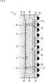
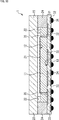
図1のイメージセンサパッケージ1は、シリコン基板等の半導体基板(不図示)にフォトダイオード(光電変換素子)、トランジスタ等の半導体素子が形成されたイメージセンサ11を含んで構成される。イメージセンサ11は、例えば、裏面照射型のCMOS(Complementary Metal Oxide Semiconductor)イメージセンサなどである。
The
図1においてイメージセンサ11の光入射面側となる第1の主面12側には、オンチップレンズ21が形成されている。オンチップレンズ21の上方には、可視光の透過率が高い光透過性部材22が配置され、この光透過性部材22を介してガラス基板23が配置されている。光透過性部材22には、その屈折率が、例えば、0.5乃至3.0程度の材料を用いることができるが、ガラス基板23の屈折率に近い屈折率であればさらに好ましい。
An on-
光透過性部材22とガラス基板23により、イメージセンサ11の受光部を埃やダストなどから保護することができる。ここで、イメージセンサ11の受光部とは、例えば、フォトダイオード、カラーフィルタ、オンチップレンズなどの、光が入射(通過)される部分である。
The
イメージセンサ11の側面には、被覆部24が配置され、被覆部24とイメージセンサ11の上側に、ガラス基板23が配置されている。被覆部24は、例えば、可視光から近赤外までの光の透過率が10%以下の遮光性を有する樹脂材料(以下、単に遮光材料という。)で形成することができる。あるいはまた、被覆部24は、熱伝導率が0.5W/m・K以上の高熱伝導性を有する樹脂材料(以下、放熱材料という。)で形成することができる。
A covering
ガラス基板23には、ガラス基板23から発生するα線がイメージセンサ11の受光部に入射することを防止するアクリルなどの膜(図示せず)や、入射光の赤外成分を除去する赤外線カットフィルタ(図示せず)、入射光の反射を防止する光学膜(図示せず)などが形成されても良い。
The
イメージセンサ11の下側となる第2の主面13側には、再配線層31(RDL:Re-distribution Layer)が形成されている。この再配線層31も、被覆部24とイメージセンサ11とからなる平面領域に対応して形成されている。イメージセンサ11の第2の主面13と被覆部24の面とは平坦な面となっており、再配線層31が形成しやすくなっている。
A rewiring layer 31 (RDL: Re-distribution Layer) is formed on the second
なお、以下では、イメージセンサ11の下側となる第2の主面13側を、イメージセンサ11の背面とも称する。
In the following, the second
再配線層31は、複数の金属配線層32とその間に形成された絶縁層33とからなる。各金属配線層32どうしは、絶縁層33に形成された貫通孔(不図示)によって接続されている。複数の金属配線層32のうち、最下層の金属配線層32は、外部端子34と接続されている。外部端子34は、電気信号の入力若しくは出力、または、電力の供給を受けるための端子であり、例えば、金属バンプで構成される。
The
イメージセンサ11のフォトダイオードで受光されることにより生成された電荷は、半導体基板に形成された内部回路からTSV(Through Silicon Via:シリコン貫通電極)35を経由して、金属配線層32へ伝送され、外部端子34から、電気信号として出力される。
The charge generated by receiving light from the photodiode of the
このイメージセンサパッケージ1は、図29を参照して後述するように、レンズ構造体173等とともに組み立てられ、カメラモジュール151を構成する。
This
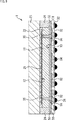
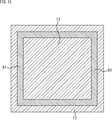
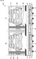
図2は、図1のイメージセンサパッケージ1を、外部端子34側からみた平面図である。
FIG. 2 is a plan view of the
図1において最下層となる金属配線層32は、図2に示されるように、イメージセンサ11の領域内に形成された電極部14から、外周部へ拡がるように形成され、イメージセンサパッケージ1の外部端子34に接続されている。このように金属配線層32を外周部へ拡がるFan-out配線として外部端子34と接続することにより、外部端子34は、被覆部24の平面領域も含む、イメージセンサ11の平面領域よりも大きな領域に配置することができる。
As shown in FIG. 2, the
よって、第1の実施の形態のイメージセンサパッケージ1によれば、イメージセンサ11のI/O数の増加に対応して、より多くの外部端子34を設けることができる。
Therefore, according to the
また、イメージセンサ11の側面が被覆部24で覆われているので、イメージセンサ11の側面を保護することができる。
Further, since the side surface of the
<1.2 第1の実施の形態の製造方法>
次に、図3を参照して、第1の実施の形態のイメージセンサパッケージ1の製造方法(第1の製造方法)について説明する。<1.2 Manufacturing method of the first embodiment>
Next, the manufacturing method (first manufacturing method) of the
初めに、半導体ウェハから個片化されたイメージセンサ11が用意される。そして、図3のAに示されるように、個片化されたイメージセンサ11がガラス基板23上に搭載される。具体的には、ガラス基板23上に光透過性部材22を、例えば塗布により形成し、その光透過性部材22の上に、個片化されたイメージセンサ11が、受光面をガラス基板23に向けるようにして、Pick and Placeで配列し、接着される。
First, an
ガラス基板23は、例えば、ウェハもしくはパネルの形態の、ホウケイ酸ガラス、石英ガラス、ソーダ石灰ガラス等で構成される。
The
次に、図3のBに示されるように、ガラス基板23のイメージセンサ11が搭載された面が、所定の被覆材料を用いて、印刷法や塗布法、ラミネート法やモールド法などによって被覆(モールド)され、被覆部24が形成される。被覆材料としては、例えば、半導体パッケージ用途の一般的なエポキシ系モールド材料などの絶縁性材料を用いることができる。
Next, as shown in B of FIG. 3, the surface of the
続いて、図3のCに示されるように、被覆部24が形成された面を、機械研削や化学機械研磨(Chemical Mechanical Polishing:CMP)等により研削することで、イメージセンサ11の第2の主面13が露出される。この研削は、イメージセンサ11の薄肉化を兼ねても良い。
Subsequently, as shown in FIG. 3C, the surface on which the covering
イメージセンサ11の第2の主面13には、デバイス回路が存在しないため、研削精度はあまり高くなくても良い。研削により、被覆部24とイメージセンサ11の第2の主面13とを平坦にすることができ、TSV35(図3では不図示)を均一に露出させることができる。これにより、イメージセンサ11のTSV35と金属配線層32との接続を精度よく加工することができる。
Since the device circuit does not exist on the second
次に、図3のDに示されるように、金属配線層32と絶縁層33を含む再配線層31、及び、外部端子34が形成される。金属配線層32には、例えば、Al, Al-Cu, Al-Si, Al-Nd, Cu, Au, Agなどが用いられる。絶縁層33には、例えば、ポリイミドやエポキシなどのポリマー、SiOxやSiNxなどの無機材料が用いられる。外部端子34と接続される金属配線層32のパッド部分には、Ni/AuやNi/Pd/Auなどの積層バリアが形成されるのが好ましい。金属配線層32と絶縁層33は、例えば、スパッタ法、CVD法、蒸着法、めっき法、印刷法等により形成することができる。外部端子34は、例えば、印刷法、蒸着法、めっき法などによって形成される金属バンプとすることができるが、金属配線層32のパッド部分をそのまま露出させた構造としてもよい。Next, as shown in D of FIG. 3, a
最後に、図3のEに示されるように、ブレードもしくはレーザーなどを活用したダイシング等により個片化を行うことで、図1に示した第1の実施の形態のイメージセンサパッケージ1が完成する。
Finally, as shown in E of FIG. 3, the
第1の製造方法では、ガラス基板23上に、イメージセンサ11が配列され、その後、再配線層31や外部端子34が形成される。一般に、ガラス基板は、熱や湿気に対する寸法安定性が高く、反りに強い。ガラス基板上への配線技術は、TFT(Thin Film Transistor)などの分野でも利用されている。第1の製造方法のように、ガラス基板23上に配線加工を行うことで、再配線層31の線幅と線間距離(Line/Space)それぞれが10μ以下となるような非常に微細な配線加工を実現することができる。
In the first manufacturing method, the
<1.3 第1の実施の形態の第1変形例>
図4は、第1の実施の形態の第1変形例を示すイメージセンサパッケージ1の断面図である。<1.3 First modification of the first embodiment>
FIG. 4 is a cross-sectional view of the
図4に示される第1の実施の形態の第1変形例では、イメージセンサ11の側面の被覆部24が、2種類の被覆部24Aと24Bに置き換えられている点が、図1に示した第1の実施の形態と異なる。
In the first modification of the first embodiment shown in FIG. 4, the point that the covering
2種類の被覆部24Aと24Bのうち、イメージセンサ11と接する被覆部24Aは、可視光から近赤外までの光の透過率が10%以下の遮光材料で形成される。一方、被覆部24Bは、熱伝導率が0.5W/m・K以上の放熱材料で形成される。
Of the two types of covering
この2種類の被覆部24Aと24Bは、図3のBに示した被覆部24を形成する工程において、初めに、被覆部24Aとなる遮光材料を用いて、印刷法、塗布法、蒸着法、ラミネート法、モールド法などによって被覆し、次いで、被覆部24Bとなる放熱材料を用いて、同様の方法で被覆することで形成することができる。
In the step of forming the covering
このように、イメージセンサ11と接する被覆部24Aを遮光材料とすることで、イメージセンサ11の側面やガラス基板23下面から入射される迷光を吸収し、意図しない光がイメージセンサ11の受光部に入射することを防ぐことができる。
By using the covering
また、被覆部24A外側の被覆部24Bを放熱材料とすることで、イメージセンサ11から発生する熱を放散するための放熱経路を形成することができる。
Further, by using the covering
なお、被覆部24は、3種類の被覆材料で構成してもよく、1種類以上の被覆材料で被覆された構造であればよい。
The covering
<1.4 第1の実施の形態の第2変形例>
図5は、第1の実施の形態の第2変形例を示すイメージセンサパッケージ1の断面図である。<1.4 Second modified example of the first embodiment>
FIG. 5 is a cross-sectional view of the
図5に示される第1の実施の形態の第2変形例では、ガラス基板23の厚みが、イメージセンサ11より外側の外周部において、イメージセンサ11の上側部分の厚みよりも厚く形成されている点が図1の第1の実施の形態と異なる。一方で、ガラス基板23が厚い部分の被覆部24の厚みは、その他の部分よりも薄く形成されている。
In the second modification of the first embodiment shown in FIG. 5, the thickness of the
イメージセンサパッケージ1の上側に配置される、入射光をイメージセンサ11の受光部に集光するための複数のレンズからなるレンズ構造体173(図29)の高さは、光路長によって決まる。光軸上に空気よりも屈折率が大きい部材があると、その分だけ光路長は大きくなり、レンズ構造体173の高さも増大する。ガラス基板23の屈折率は1.5であり、光軸上のガラス基板23の厚さx1/3程度だけ光路長は余分に大きくなり、カメラモジュール151が高くなってしまう。そのため光軸上のガラス基板23は薄いほどよいが、ガラス基板23を薄くすると剛性が低下し、イメージセンサ11が撓む場合がある。
The height of the lens structure 173 (FIG. 29), which is arranged on the upper side of the
そこで、第2変形例のように、イメージセンサ11より外側の外周部の厚みを、イメージセンサ11の上側の厚みよりも厚く形成したガラス基板23を採用することで、光軸上のガラス基板23の厚みを薄くしながら、外周部の厚いガラス部分(stiffener構造)と被覆部24によって、ガラス基板23とイメージセンサ11の剛性を保持することができる。これにより、光路長の光路長を短縮しつつ、イメージセンサ11の反りや撓みを抑制することができる。
Therefore, as in the second modification, by adopting a
<2.第2の実施の形態>
<2.1 第2の実施の形態の構造図>
図6は、本技術を適用した半導体装置の第2の実施の形態としての、イメージセンサパッケージの断面図を示している。<2. Second Embodiment>
<2.1 Structural drawing of the second embodiment>
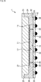
FIG. 6 shows a cross-sectional view of an image sensor package as a second embodiment of a semiconductor device to which the present technology is applied.
なお、図6においては、上述した第1の実施の形態と対応する部分については同一の符号を付してあり、第1の実施の形態と異なる部分についてのみ説明する。後述するその他の実施の形態についても同様とする。 In FIG. 6, the parts corresponding to the above-described first embodiment are designated by the same reference numerals, and only the parts different from the first embodiment will be described. The same shall apply to other embodiments described later.
図6に示される第2の実施の形態のイメージセンサパッケージ1では、イメージセンサ11の外部端子34側の面である第2の主面13と再配線層31との間に、被覆部24が形成されている点が、第1の実施の形態と異なる。
In the
また、第2の主面13と再配線層31との間の被覆部24の一部分に金属バンプ41が設けられ、イメージセンサ11のTSV35が、金属バンプ41を介して、再配線層31の金属配線層32と接続されている。金属バンプ41は、例えば、Sn-Agバンプ、Sn-Ag-Cuバンプ、Auスタッドバンプなどで構成され、その周囲は被覆部24で覆われている。
Further, a
さらに、第1の実施の形態では、光透過性部材22が、イメージセンサ11の上部のみに形成されていたが、第2の実施の形態では、光透過性部材22が、イメージセンサ11の外側の被覆部24の上部にも形成され、ガラス基板23の下面全領域と接している。
Further, in the first embodiment, the
第2の実施の形態におけるイメージセンサパッケージ1を外部端子34側からみた平面図の図示は省略するが、図2と同様に、金属配線層32は、外周部へ拡がるFan-out配線として形成され、外部端子34と接続されている。
Although the plan view of the
したがって、第2の実施の形態においても、第1の実施の形態と同様に、金属配線層32を外周部へ拡がるFan-out配線としたことにより、イメージセンサ11のI/O数の増加に対応して、より多くの外部端子34を設けることができる。
Therefore, also in the second embodiment, the number of I / O of the
また、イメージセンサ11の側面と背面が被覆部24で覆われているので、イメージセンサ11の側面と背面を同時に保護することができる。
Further, since the side surface and the back surface of the
図6の例では、被覆部24が1種類の樹脂材料で形成されているが、第1の実施の形態の第1変形例と同様に2種類以上の樹脂材料の積層により被覆部24が形成されてもよい。
In the example of FIG. 6, the covering
<2.2 第2の実施の形態の製造方法>
次に、図7を参照して、第2の実施の形態のイメージセンサパッケージ1の製造方法(第2の製造方法)について説明する。<2.2 Manufacturing method of the second embodiment>
Next, the manufacturing method (second manufacturing method) of the
初めに、個片化されたイメージセンサ11が用意される。用意されるイメージセンサ11は、図7のAに示されるように、第1の主面12側に形成されたオンチップレンズ21が、除去可能な保護膜42で保護され、第2の主面13側に金属バンプ41が形成されたイメージセンサである。
First, an
そして、用意されたイメージセンサ11が、図7のAに示されるように、紫外線(UV)で剥離可能な接着剤52を介して再配線層31を形成したキャリア基板51に、フリップチップ実装される。より詳しくは、再配線層31の最表面の金属配線層32上に、イメージセンサ11の金属バンプ41が配置されるようにして、金属バンプ41と金属配線層32がフリップチップ接合(Flip Chip Bonding)される。キャリア基板51は、ガラス基板23と同様、例えば、ウェハもしくはパネルの形態の石英ガラスなどで構成される。
Then, as shown in A of FIG. 7, the
図3のAと図7のAを比較して明らかなように、図3に示した第1の製造方法では、イメージセンサ11がガラス基板23に対して受光面が向くように接着されたのに対して、第2の製造方法では、イメージセンサ11が、キャリア基板51に対して、受光面が上向きとなるようにフリップチップ実装される。
As is clear by comparing A in FIG. 3 and A in FIG. 7, in the first manufacturing method shown in FIG. 3, the
次に、図7のBに示されるように、キャリア基板51上のイメージセンサ11が搭載された面が所定の被覆材料を用いて、印刷法や塗布法、ラミネート法やモールド法などによって被覆され、被覆部24が形成される。被覆材料としては、例えば、半導体パッケージ用途の一般的なエポキシ系モールド材料などを用いることができる。
Next, as shown in B of FIG. 7, the surface on the
次に、図7のCに示されるように、機械研削や化学機械研磨により、イメージセンサ11に形成した保護膜42が露出されるまで、被覆部24が平坦に研磨された後、保護膜42が除去される。被覆部24の研削では、保護膜42が露出される研削を行えば良いため、研削精度はあまり高くなくても良い。
Next, as shown in C of FIG. 7, the covering
次に、図7のDに示されるように、接着剤となる光透過性部材22を用いて、ガラス基板23と、イメージセンサ11が実装されたキャリア基板51が、Wafer to Waferで貼り合わされる。
Next, as shown in D of FIG. 7, the
続いて、図7のEに示されるように、キャリア基板51の裏面側から紫外線(UV)を照射して、キャリア基板51が剥離される。キャリア基板51が剥離されると、ガラス基板23に受光面を向けて、イメージセンサ11が配列された基板構造が出来上がる。イメージセンサ11の側面は、被覆部24で被覆され、イメージセンサ11の第2の主面13側には、再配線層31が形成されている。
Subsequently, as shown in E of FIG. 7, the
最後に、図7のFに示されるように、ブレードもしくはレーザーなどを活用したダイシング等により個片化を行うことで、図6に示した第2の実施の形態のイメージセンサパッケージ1が完成する。
Finally, as shown in F of FIG. 7, the
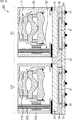
<3.第3の実施の形態>
<3.1 第3の実施の形態の構造図>
図8は、本技術を適用した半導体装置の第3の実施の形態としての、イメージセンサパッケージの断面図を示している。<3. Third Embodiment>
<3.1 Structural drawing of the third embodiment>
FIG. 8 shows a cross-sectional view of an image sensor package as a third embodiment of a semiconductor device to which the present technology is applied.
図8に示される第3の実施の形態のイメージセンサパッケージ1では、イメージセンサ11の外部端子34側の面である第2の主面13と再配線層31との間に、被覆部55が新たに形成されている点が、第1の実施の形態と異なる。この被覆部55は、図9を参照して後述するように、イメージセンサ11の側面に形成された被覆部24とは別工程で形成されるが、被覆部55と被覆部24の材料は同一でもよい。あるいはまた、図4に示した第1の実施の形態の第1変形例のように、被覆部24と被覆部55の一方を遮光材料とし、他方を放熱材料とするなど、被覆部55と被覆部24で異なる特性の材料を用いてもよい。
In the
イメージセンサ11のTSV35は、被覆部55と同じ層に設けられたビア56を介して、再配線層31の金属配線層32と接続されている。ビア56の周囲は被覆部55で覆われている。
The
第3の実施の形態におけるイメージセンサパッケージ1を外部端子34側からみた平面図の図示は省略するが、図2と同様に、金属配線層32は、外周部へ拡がるFan-out配線として形成され、外部端子34と接続されている。
Although the plan view of the
したがって、第3の実施の形態においても、第1の実施の形態と同様に、金属配線層32を外周部へ拡がるFan-out配線としたことにより、イメージセンサ11のI/O数の増加に対応して、より多くの外部端子34を設けることができる。
Therefore, in the third embodiment as well, as in the first embodiment, the fan-out wiring that extends the
また、イメージセンサ11の側面と背面が被覆部24または55で覆われているので、イメージセンサ11の側面と背面を同時に保護することができる。
Further, since the side surface and the back surface of the
<3.2 第3の実施の形態の製造方法>
次に、図9を参照して、第3の実施の形態のイメージセンサパッケージ1の製造方法(第3の製造方法)について説明する。<3.2 Manufacturing method of the third embodiment>
Next, the manufacturing method (third manufacturing method) of the
図9のA乃至Cの工程は、図3のA乃至Cの工程と同様である。 The steps A to C in FIG. 9 are the same as the steps A to C in FIG.
即ち、初めに、図9のAに示されるように、個片化されたイメージセンサ11がガラス基板23上に搭載される。
That is, first, as shown in A of FIG. 9, the
次に、図9のBに示されるように、ガラス基板23のイメージセンサ11が搭載された面が、所定の被覆材料を用いて、印刷法や塗布法、ラミネート法やモールド法などによって被覆され、被覆部24が形成される。被覆材料としては、例えば、半導体パッケージ用途の一般的なエポキシ系モールド材料などを用いることができる。
Next, as shown in B of FIG. 9, the surface of the
続いて、図9のCに示されるように、被覆部24が形成された面を、機械研削や化学機械研磨等により研削することで、イメージセンサ11の第2の主面13が露出される。
Subsequently, as shown in FIG. 9C, the surface on which the covering
次に、図9のDに示されるように、露出されたイメージセンサ11の第2の主面13を含む面全体が、所定の被覆材料を用いて、印刷法、塗布法、蒸着法、または、ラミネート法などによって被覆され、被覆部55が形成される。再被覆する面は平坦であるため、再被覆後の面も平坦性を維持することができる。
Next, as shown in D of FIG. 9, the entire surface including the second
次いで、図9のDに示されるように、この被覆部55で被膜された面のうち、イメージセンサ11のTSV35が配置された位置を開口し、金属材料を埋め込む、または、開口部にコンフォーマルに金属材料を形成するなどにより、ビア56が形成される。開口部の形成は、例えば、ウェットエッチング、ドライエッチング、機械ドリル加工、レーザードリル加工などによって行うことができる。
Next, as shown in D of FIG. 9, on the surface coated by the covering
図9のE及びFの工程は、図3のD及びEを参照して説明した工程と同様である。 The steps E and F in FIG. 9 are the same as the steps described with reference to D and E in FIG.
即ち、図9のEに示されるように、被覆部55とビア56が形成された平坦面の上に、金属配線層32と絶縁層33を含む再配線層31、及び、外部端子34が形成される。そして、図9のFに示されるように、ブレードもしくはレーザーなどを活用したダイシング等により個片化を行うことで、図8に示した第3の実施の形態のイメージセンサパッケージ1が完成する。
That is, as shown in E of FIG. 9, the
第3の製造方法においても、ガラス基板23上に再配線層31を形成するので、第1の製造方法と同様に、非常に微細な配線加工を実現することができる。
Also in the third manufacturing method, since the
<4.第4の実施の形態>
<4.1 第4の実施の形態の構造図>
図10は、本技術を適用した半導体装置の第4の実施の形態としての、イメージセンサパッケージの断面図を示している。<4. Fourth Embodiment>
<4.1 Structural drawing of the fourth embodiment>
FIG. 10 shows a cross-sectional view of an image sensor package as a fourth embodiment of a semiconductor device to which the present technology is applied.
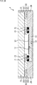
図10に示される第4の実施の形態のイメージセンサパッケージ1では、ガラス基板23とイメージセンサ11との間に、複数の金属配線層61とその間に形成された絶縁層62とからなる配線層63が配置されている。配線層63は、イメージセンサ11の第1の主面12上に形成された金属バンプ71と接合されている。金属バンプ71の周囲には、アンダーフィル72が形成されている。配線層63は、ガラス基板23とイメージセンサ11の金属バンプ71の両方と接続する役割を有するものであり、特に信号処理を行う回路が形成されていなくてもよい。
In the
金属バンプ71とアンダーフィル72は、図11に示されるように、イメージセンサ11の第1の主面12上の周縁部に、外周を囲むように配置されており、図10において、イメージセンサ11と、その上の配線層63及びガラス基板23とで囲まれる空間が、アンダーフィル72によって封止されている。これにより、イメージセンサ11の受光部を埃やダストなどから保護することができる。
As shown in FIG. 11, the
配線層63を構成する金属配線層61及び絶縁層62は、上述した再配線層31の金属配線層32及び絶縁層33と同様の材料を用いて形成されている。また、各金属配線層61どうしは、絶縁層62に形成された貫通孔(不図示)によって接続されている。
The
イメージセンサ11の側面は、被覆部24で覆われている。
The side surface of the
第4の実施の形態におけるイメージセンサパッケージ1を外部端子34側からみた平面図の図示は省略するが、図2と同様に、金属配線層32は、外周部へ拡がるFan-out配線として形成され、外部端子34と接続されている。
Although the plan view of the
したがって、第4の実施の形態においても、第1の実施の形態と同様に、金属配線層32を外周部へ拡がるFan-out配線としたことにより、イメージセンサ11のI/O数の増加に対応して、より多くの外部端子34を設けることができる。
Therefore, also in the fourth embodiment, the number of I / O of the
また、イメージセンサ11の側面が被覆部24で覆われているので、イメージセンサ11の側面を保護することができる。
Further, since the side surface of the
<4.2 第4の実施の形態の製造方法>
次に、図12を参照して、第4の実施の形態のイメージセンサパッケージ1の製造方法(第4の製造方法)について説明する。<4.2 Manufacturing method of the fourth embodiment>
Next, a manufacturing method (fourth manufacturing method) of the
初めに、個片化されたイメージセンサ11が用意される。第4の製造方法において用意されるイメージセンサ11は、図12のAに示されるように、オンチップレンズ21が形成された第1の主面12側に金属バンプ71が形成されたイメージセンサ11である。金属バンプ71は、第2の実施の形態と同様に、例えば、Sn-Agバンプ、Sn-Ag-Cuバンプ、Auスタッドバンプなどで構成される。
First, an
また、第4の製造方法においては、金属バンプ71が形成されたイメージセンサ11の他、基板上に配線層63が形成されたガラス基板23が用意される。
Further, in the fourth manufacturing method, in addition to the
そして、用意されたイメージセンサ11が、図12のAに示されるように、ガラス基板23上に形成された配線層63の金属配線層61に、フリップチップ実装される。すなわち、配線層63の最表面の金属配線層61上に、イメージセンサ11の金属バンプ71が配置されるようにして、金属バンプ71と金属配線層61がフリップチップ接合(Flip Chip Bonding)される。
Then, as shown in A of FIG. 12, the
また、図11に示したようにイメージセンサ11の外周を囲むように、フリップチップ接合された金属バンプ71の周囲に、アンダーフィル72が形成される。
Further, as shown in FIG. 11, an
各金属配線層61の底面のみもしくは底面と上面の両方には、バリア層として高抵抗金属(Ti, TiN, Mo, Mo-Nbなど)が形成される場合もある。
A high resistance metal (Ti, TiN, Mo, Mo-Nb, etc.) may be formed as a barrier layer only on the bottom surface of each
図12のB乃至Eに示される各工程は、図3のB乃至Eに示した各工程と同様である。 Each step shown in B to E of FIG. 12 is the same as each step shown in B to E of FIG.
即ち、図12のBに示されるように、ガラス基板23のイメージセンサ11が搭載された面が、所定の被覆材料を用いて、印刷法や塗布法、ラミネート法やモールド法などによって被覆され、被覆部24が形成される。被覆材料としては、例えば、半導体パッケージ用途の一般的なエポキシ系モールド材料などを用いることができる。
That is, as shown in B of FIG. 12, the surface of the
続いて、図12のCに示されるように、被覆部24が形成された面を、機械研削や化学機械研磨等により研削することで、イメージセンサ11の第2の主面13が露出される。
Subsequently, as shown in FIG. 12C, the surface on which the covering
次に、図12のDに示されるように、金属配線層32と絶縁層33を含む再配線層31、及び、外部端子34が形成される。
Next, as shown in D of FIG. 12, a
最後に、図12のEに示されるように、ブレードもしくはレーザーなどを活用したダイシング等により個片化を行うことで、図10に示した第4の実施の形態のイメージセンサパッケージ1が完成する。
Finally, as shown in E of FIG. 12, the
第4の製造方法においても、ガラス基板23上に配線層63や再配線層31を形成するので、第1の製造方法と同様に、非常に微細な配線加工を実現することができる。
Also in the fourth manufacturing method, since the
<4.3 第4の実施の形態の第1変形例>
図13は、第4の実施の形態の第1変形例を示すイメージセンサパッケージ1の断面図である。<4.3 First modification of the fourth embodiment>
FIG. 13 is a cross-sectional view of the
図13に示した第4の実施の形態おいて、イメージセンサ11と、その上の配線層63及びガラス基板23とで囲まれた空間には、空気が封入されていたのに対して、図13に示される第4の実施の形態の第1変形例では、光透過性部材22が封入されている。光透過性部材22が封入されたことにより、第4の実施の形態のアンダーフィル72が省略されている。
In the fourth embodiment shown in FIG. 13, air is sealed in the space surrounded by the
光透過性部材22には、その屈折率が、例えば、0.5乃至3.0程度の材料を用いることができるが、ガラス基板23の屈折率に近い屈折率であればさらに好ましい。
For the
光透過性部材22とガラス基板23により、イメージセンサ11の受光部を埃やダストなどから保護することができる。
The
<4.4 第4の実施の形態の第2変形例>
図14は、第4の実施の形態の第2変形例を示すイメージセンサパッケージ1の断面図である。<4.4 Second modification of the fourth embodiment>
FIG. 14 is a cross-sectional view of the
図14に示される第4の実施の形態の第2変形例では、図10に示した第4の実施の形態の金属バンプ71とアンダーフィル72が、金属部材81に置き換えられている。この金属部材81は、図15に示されるように、イメージセンサ11の外周を囲むように配置されている。図15は、イメージセンサ11の第1の主面12側から金属部材81を見た平面図である。
In the second modification of the fourth embodiment shown in FIG. 14, the
このように、金属部材81によりイメージセンサ11の受光部を囲むことによっても、イメージセンサ11の受光部を埃やダストなどから保護することができる。
By surrounding the light receiving portion of the
<4.5 第4の実施の形態の第3変形例>
図16は、第4の実施の形態の第3変形例を示すイメージセンサパッケージ1の断面図である。<4.5 Third Modified Example of the Fourth Embodiment>
FIG. 16 is a cross-sectional view of the
図16に示される第4の実施の形態の第3変形例では、図10に示した第4の実施の形態の金属バンプ71とアンダーフィル72が、光透過性部材22に置き換えられている。この光透過性部材22は、図15に示した金属部材81の配置と同様に、イメージセンサ11の外周を囲むように配置されている。
In the third modification of the fourth embodiment shown in FIG. 16, the
光透過性部材22は、イメージセンサ11とガラス基板23とを接着する接着剤の役割を果たすので、図16の第3変形例では、配線層63は省略されている。
Since the
このように、光透過性部材22によりイメージセンサ11の受光部を囲むことによっても、イメージセンサ11の受光部を埃やダストなどから保護することができる。
By surrounding the light receiving portion of the
<5.第5の実施の形態>
<5.1 第5の実施の形態の構造図>
図17は、本技術を適用した半導体装置の第5の実施の形態としての、イメージセンサパッケージの断面図を示している。<5. Fifth Embodiment>
<Structural diagram of 5.1 fifth embodiment>
FIG. 17 shows a cross-sectional view of an image sensor package as a fifth embodiment of a semiconductor device to which the present technology is applied.
図17に示される第5の実施の形態のイメージセンサパッケージ1では、イメージセンサ11の外部端子34側の面である第2の主面13と再配線層31との間に、被覆部55とビア56が形成されている点が、図10に示した第4の実施の形態と異なる。
In the
被覆部55は、上述した第3の実施の形態と同様に、イメージセンサ11の側面に形成された被覆部24とは別工程で形成されるが、被覆部55と被覆部24の材料は同一でも異なっていてもよい。
The covering
イメージセンサ11のTSV35は、被覆部55と同じ層に設けられたビア56を介して、再配線層31の金属配線層32と接続されている。ビア56の周囲は被覆部55で覆われている。
The
なお、図17に示される第5の実施の形態では、イメージセンサ11の側面に形成された被覆部24の上面は配線層63のみと接しているのに対して、図10の第4の実施の形態では、被覆部24の上面の一部がガラス基板23と接しているが、この被覆部24の形態はどちらを採用してもよい。逆に言うと、図10の第4の実施の形態において、被覆部24の上面が配線層63のみと接するように構成してもよいし、図17の第5の実施の形態において、被覆部24の上面がガラス基板23と配線層63の両方と接するように構成してもよい。
In the fifth embodiment shown in FIG. 17, the upper surface of the covering
第5の実施の形態においても、再配線層31の金属配線層32は、外周部へ拡がるFan-out配線として形成され、外部端子34と接続されている。
Also in the fifth embodiment, the
したがって、第5の実施の形態においても、上述したその他の実施の形態と同様に、イメージセンサ11のI/O数の増加に対応して、より多くの外部端子34を設けることができる。また、イメージセンサ11の側面が被覆部24で覆われているので、イメージセンサ11の側面を保護することができる。
Therefore, also in the fifth embodiment, as in the other embodiments described above, more
<5.2 第5の実施の形態の製造方法>
次に、図18を参照して、第5の実施の形態のイメージセンサパッケージ1の製造方法(第5の製造方法)について説明する。<5.2 Manufacturing method of the fifth embodiment>
Next, a manufacturing method (fifth manufacturing method) of the
図18のA乃至Cの工程は、図12のA乃至Cの工程と同様である。 The steps A to C in FIG. 18 are the same as the steps A to C in FIG.
初めに、図18のAに示されるように、金属バンプ71付きの個片化されたイメージセンサ11が、配線層63が形成されたガラス基板23の金属配線層61上にフリップチップ接合された後、アンダーフィル72が形成される。
First, as shown in FIG. 18A, an
次に、図18のBに示されるように、ガラス基板23のイメージセンサ11が搭載された面が、所定の被覆材料を用いて、印刷法や塗布法、ラミネート法やモールド法などによって被覆され、被覆部24が形成される。被覆材料としては、例えば、半導体パッケージ用途の一般的なエポキシ系モールド材料などを用いることができる。
Next, as shown in FIG. 18B, the surface of the
続いて、図18のCに示されるように、被覆部24が形成された面を、機械研削や化学機械研磨等により研削することで、イメージセンサ11の第2の主面13が露出される。
Subsequently, as shown in FIG. 18C, the surface on which the covering
次に、図18のDに示されるように、露出されたイメージセンサ11の第2の主面13を含む面全体が、所定の被覆材料を用いて、印刷法、塗布法、蒸着法、または、ラミネート法などによって被覆され、被覆部55が形成される。再被覆する面は平坦であるため、再被覆後の面も平坦性を維持することができる。
Next, as shown in D of FIG. 18, the entire surface including the second
次いで、図18のDに示されるように、この被覆部55で被膜された面のうち、イメージセンサ11のTSV35が配置された位置を開口し、金属材料を埋め込む、または、開口部にコンフォーマルに金属材料を形成するなどにより、ビア56が形成される。開口部の形成は、例えば、ウェットエッチング、ドライエッチング、機械ドリル加工、レーザードリル加工などによって行うことができる。
Next, as shown in D of FIG. 18, on the surface coated by the covering
その後、図18のEに示されるように、被覆部55とビア56が形成された平坦面の上に、金属配線層32と絶縁層33を含む再配線層31、及び、外部端子34が形成される。そして、図18のFに示されるように、ブレードもしくはレーザーなどを活用したダイシング等により個片化を行うことで、図17に示した第5の実施の形態のイメージセンサパッケージ1が完成する。
After that, as shown in E of FIG. 18, the
第5の製造方法においても、ガラス基板23上に再配線層31を形成するので、上述したその他の製造方法と同様に、非常に微細な配線加工を実現することができる。
Also in the fifth manufacturing method, since the
<6.第6の実施の形態>
<6.1 第6の実施の形態の構造図>
図19は、本技術を適用した半導体装置の第6の実施の形態としての、イメージセンサパッケージの断面図を示している。<6. 6th Embodiment>
<6.1 Structural drawing of the sixth embodiment>
FIG. 19 shows a cross-sectional view of an image sensor package as a sixth embodiment of a semiconductor device to which the present technology is applied.
図19に示される第6の実施の形態のイメージセンサパッケージ1では、図1に示した第1の実施の形態と比較すると、被覆部24が、イメージセンサ11の側面だけではなく、ガラス基板23の側面も覆うように形成されている点が異なる。第6の実施の形態のその他の構造は、図1に示した第1の実施の形態と同様である。
In the
第6の実施の形態のイメージセンサパッケージ1では、被覆部24が、イメージセンサ11の側面だけではなく、ガラス基板23の側面も覆うように形成されていることにより、イメージセンサ11とガラス基板23の両方の端面を保護することができる。
In the
また、ガラス基板23の側面で入射または反射してイメージセンサ11の受光部に入射する迷光を防止することができ、イメージセンサ11からの放熱経路を形成することができる。
Further, it is possible to prevent stray light incident or reflected on the side surface of the
さらに、第1の実施の形態と同様に、金属配線層32を外周部へ拡がるFan-out配線としたことにより、イメージセンサ11のI/O数の増加に対応して、より多くの外部端子34を設けることができる。
Further, as in the first embodiment, the
<6.2 第6の実施の形態の製造方法>
次に、図20を参照して、第6の実施の形態のイメージセンサパッケージ1の製造方法(第6の製造方法)について説明する。<6.2 Manufacturing method of the sixth embodiment>
Next, the manufacturing method (sixth manufacturing method) of the
初めに、半導体ウェハから個片化されたイメージセンサ11が用意される。そして、図20のAに示されるように、個片化されたイメージセンサ11がガラス基板23上に搭載される。具体的には、ガラス基板23上に光透過性部材22を、例えば塗布により形成し、その光透過性部材22の上に、個片化されたイメージセンサ11が、受光面をガラス基板23に向けるようにして、Pick and Placeで配列し、接着される。
First, an
次に、図20のBに示されるように、配列されたイメージセンサ11どうしの間のガラス基板23が所定の深さまで掘り込まれ、溝部91が形成される。溝部91の幅は数10μmから数100μm、深さは数10um以上の任意の値とされる。
Next, as shown in FIG. 20B, the
そして、図20のCに示されるように、溝部91を含むガラス基板23とイメージセンサ11の上面が、所定の被覆材料を用いて、印刷法や塗布法、ラミネート法やモールド法などによって被覆され、被覆部24が形成される。被覆材料としては、例えば、半導体パッケージ用途の一般的なエポキシ系モールド材料などを用いることができる。
Then, as shown in C of FIG. 20, the upper surface of the
続いて、図20のDに示されるように、イメージセンサ11の第2の主面13が露出されるまで、被覆部24が、機械研削や化学機械研磨等により研削される。この研削は、イメージセンサ11の薄肉化を兼ねても良い。
Subsequently, as shown in D of FIG. 20, the covering
イメージセンサ11の第2の主面13には、デバイス回路が存在しないため、研削精度はあまり高くなくても良い。研削により、被覆部24とイメージセンサ11の第2の主面13とを平坦にすることができ、TSV35(図20では不図示)を均一に露出させることができる。これにより、イメージセンサ11のTSV35と金属配線層32との接続を精度よく加工することができる。
Since the device circuit does not exist on the second
次に、図20のEに示されるように、金属配線層32と絶縁層33を含む再配線層31、及び、外部端子34が形成される。
Next, as shown in E of FIG. 20, a
続いて、図20のFに示されるように、ガラス基板23が、イメージセンサ11ごとに分断されるまで、HFスリミングなどによって薄化される。
Subsequently, as shown in F of FIG. 20, the
最後に、図20のGに示されるように、ブレードもしくはレーザーなどを活用したダイシング等により個片化を行うことで、図19に示した第6の実施の形態のイメージセンサパッケージ1が完成する。
Finally, as shown in G of FIG. 20, the
上述した第6の製造方法は、図20のBに示した溝部91の加工と、図20のFに示したガラス基板23の薄化の工程が追加された以外は、図3を参照して説明した第1の製造方法と同様である。
Refer to FIG. 3 in the above-described sixth manufacturing method, except that the processing of the
<6.3 第6の実施の形態の変形例>
図20のFに示したガラス基板23の薄化の工程では、ガラス基板23が、イメージセンサ11ごとに分断されるまで薄化するようにしたが、完全に分断されるまで薄化しなくてもよい。<6.3 Modified example of the sixth embodiment>
In the step of thinning the
この場合、溝部91においても、所定の厚みでガラス基板23が残ることになり、図21に示されるような、ガラス基板23の端部において板厚がイメージセンサ11上方よりも薄く形成されたイメージセンサパッケージ1を製造することができる。
In this case, the
ガラス基板23の薄化の工程で完全に分断しない場合には、薄化後の各工程において、ガラス基板23が分断されないことで、基板の剛性を維持でき、かつ、被覆部24の収縮による基板全体の収縮を抑制することができるなどのメリットがある。
When the
<7.第7の実施の形態>
<7.1 第7の実施の形態の構造図>
図22は、本技術を適用した半導体装置の第7の実施の形態としての、イメージセンサパッケージの断面図を示している。<7. Seventh Embodiment>
<7.1 Structural drawing of the seventh embodiment>
FIG. 22 shows a cross-sectional view of an image sensor package as a seventh embodiment of a semiconductor device to which the present technology is applied.
図22に示される第7の実施の形態のイメージセンサパッケージ1では、図10に示した第4の実施の形態と比較すると、被覆部24が、イメージセンサ11の側面だけではなく、ガラス基板23の側面も覆うように形成されている点が異なる。第7の実施の形態のその他の構造は、図10に示した第4の実施の形態と同様である。
In the
第7の実施の形態のイメージセンサパッケージ1では、被覆部24が、イメージセンサ11の側面だけではなく、ガラス基板23の側面も覆うように形成されていることにより、イメージセンサ11とガラス基板23の両方の端面を保護することができる。
In the
また、ガラス基板23の側面で入射または反射してイメージセンサ11の受光部に入射する迷光を防止することができる。イメージセンサ11からの放熱経路を形成することもできる。
Further, it is possible to prevent stray light that is incident or reflected on the side surface of the
さらに、第1の実施の形態と同様に、金属配線層32を外周部へ拡がるFan-out配線としたことにより、イメージセンサ11のI/O数の増加に対応して、より多くの外部端子34を設けることができる。
Further, as in the first embodiment, the
<7.2 第7の実施の形態の製造方法>
次に、図23を参照して、第7の実施の形態のイメージセンサパッケージ1の製造方法(第7の製造方法)について説明する。<7.2 Manufacturing method of the seventh embodiment>
Next, a manufacturing method (seventh manufacturing method) of the
初めに、図23のAに示されるように、第4の製造方法として説明した図12のAの工程と同様に、金属バンプ71付きのイメージセンサ11がフリップチップ接合されたガラス基板23が、剥離可能な接着剤102を介して支持材101に貼り付けられる。支持材101は、図7のキャリア基板51と同様、例えば、ウェハもしくはパネルの形態の石英基板やテープなどで構成される。接着剤102は、例えば、紫外線(UV)を照射することで剥離可能な接着剤を用いることができる。
First, as shown in A of FIG. 23, the
次に、図23のBに示されるように、配列されたイメージセンサ11どうしの間のガラス基板23が所定の深さまで掘り込まれ、ガラス基板23が、イメージセンサ11ごとに分断される。
Next, as shown in B of FIG. 23, the
このガラス基板23の切断工程においては、図23のBのように支持材101があることで、ガラス基板23を完全に分断しても、一枚のウェハもしくはパネルのように扱うことができ、その後の一括した加工が可能となる。これによって、図20を参照して説明した第6の製造方法のように、ガラス基板23の薄化の工程を行わずにガラス基板23を分断し、ガラス基板23の側面を被覆することが可能となる。また、支持材101として、例えば、石英基板のような、熱や湿気等に対する寸法安定性の高い材料を用いることで、被覆工程などにおけるガラス基板23の反りを低減することが可能となる。
In the cutting process of the
次の図23のC乃至Eに示される各工程は、図12のB乃至Dに示した各工程と同様である。 The steps shown in C to E in FIG. 23 below are the same as the steps shown in B to D in FIG.
即ち、図23のCに示されるように、ガラス基板23のイメージセンサ11が搭載された面が、所定の被覆材料を用いて、印刷法や塗布法、ラミネート法やモールド法などによって被覆され、被覆部24が形成される。被覆材料としては、例えば、半導体パッケージ用途の一般的なエポキシ系モールド材料などを用いることができる。
That is, as shown in C of FIG. 23, the surface of the
続いて、図23のDに示されるように、被覆部24が形成された面を、機械研削や化学機械研磨等により研削することで、イメージセンサ11の第2の主面13が露出される。
Subsequently, as shown in D of FIG. 23, the surface on which the covering
次に、図23のEに示されるように、金属配線層32と絶縁層33を含む再配線層31、及び、外部端子34が形成される。
Next, as shown in E of FIG. 23, the
そして、図23のFに示されるように、接着剤102で接着されている支持材101が剥離され、図23のGに示さるように、ブレードもしくはレーザーなどを活用したダイシング等により個片化を行うことで、図22に示した第7の実施の形態のイメージセンサパッケージ1が完成する。
Then, as shown in F of FIG. 23, the
なお、第7の実施の形態のイメージセンサパッケージ1は、図20を参照して説明した第6の製造方法のように、ガラス基板23の溝加工と薄化の工程を行う方法によっても製造することができる。
The
<8.第8の実施の形態>
<8.1 第8の実施の形態の構造図>
図24は、本技術を適用した半導体装置の第8の実施の形態としての、イメージセンサパッケージの断面図を示している。<8. Eighth Embodiment>
<8.1 Structural diagram of the eighth embodiment>
FIG. 24 shows a cross-sectional view of an image sensor package as an eighth embodiment of a semiconductor device to which the present technology is applied.
図24に示される第8の実施の形態のイメージセンサパッケージ1では、図10に示した第4の実施の形態と比較すると、イメージセンサ11の第2の主面13側の再配線層31と外部端子34が、被覆部24に置き換えられている。換言すれば、第8の実施の形態では、被覆部24が、イメージセンサ11の側面に加えて背面も覆うように形成されている。また、被覆部24は、ガラス基板23の側面も覆うように形成されている。第8の実施の形態のその他の構造は、図10に示した第4の実施の形態と同様である。
In the
図24の構造を採用した場合、外部端子は、ガラス基板23の上面、または、イメージセンサパッケージ1の下面(背面)などに配置することができる。ガラス基板23の上面に配置された外部端子は、例えば、ガラス基板23を貫通するTGV(Through Glass Via, 図示せず)及び配線層63を介してイメージセンサ11と電気的に接続される。イメージセンサパッケージ1の下面に配置された外部端子は、被覆部24を貫通するTMV(Through Mold Via, 図示せず)を介してイメージセンサ11と電気的に接続される。
When the structure of FIG. 24 is adopted, the external terminals can be arranged on the upper surface of the
第8の実施の形態では、上述した第1乃至第7の実施の形態のように、イメージセンサ11の背面に、Fan-out配線を用いた再配線層31は形成されていない。代わりに、イメージセンサ11の背面も被覆部24で覆うようにしたことにより、イメージセンサ11からの放熱経路がより多く確保されている。
In the eighth embodiment, unlike the first to seventh embodiments described above, the
また、イメージセンサ11の側面及び背面とガラス基板23の側面を被覆部24で覆うように形成したことにより、イメージセンサ11の背面やガラス基板23の側面などの外部から入射する迷光や、受光した入射光がガラス基板23表面で全反射しながら側面まで伝わり、側面で反射して再度全反射を繰り返してイメージセンサ11の受光部に到達するような迷光などを吸収し、意図しない光がイメージセンサ受光部に入射することを防ぐことができる。
Further, by forming the side surface and the back surface of the
さらに、被覆部24が、イメージセンサ11とガラス基板23の側面を覆うように形成されていることにより、イメージセンサ11とガラス基板23の両方の端面を保護することができる。
Further, since the covering
<8.2 第8の実施の形態の製造方法>
次に、図25を参照して、第8の実施の形態のイメージセンサパッケージ1の製造方法(第8の製造方法)について説明する。<8.2 Manufacturing method of the eighth embodiment>
Next, with reference to FIG. 25, a manufacturing method (eighth manufacturing method) of the
初めに、図25のAに示されるように、金属バンプ71付きの個片化されたイメージセンサ11が、配線層63が形成されたガラス基板23の金属配線層61上にフリップチップ接合された後、アンダーフィル72が形成される。
First, as shown in FIG. 25A, an
次に、図25のBに示されるように、配列されたイメージセンサ11どうしの間のガラス基板23が所定の深さまで掘り込まれ、溝部91が形成される。溝部91の幅は数10μmから数100μm、深さは数10um以上の任意の値とされる。
Next, as shown in FIG. 25B, the
そして、図25のCに示されるように、溝部91及び配線層63を含むガラス基板23とイメージセンサ11の上面が、所定の被覆材料を用いて、印刷法や塗布法、ラミネート法やモールド法などによって被覆され、被覆部24が形成される。被覆材料としては、例えば、半導体パッケージ用途の一般的なエポキシ系モールド材料などを用いることができる。
Then, as shown in C of FIG. 25, the upper surface of the
続いて、図25のDに示されるように、ガラス基板23が、イメージセンサ11ごとに分断されるまで、HFスリミングなどによって薄化される。
Subsequently, as shown in D of FIG. 25, the
最後に、図25のEに示されるように、ブレードもしくはレーザーなどを活用したダイシング等により個片化を行うことで、図24に示した第8の実施の形態のイメージセンサパッケージ1が完成する。
Finally, as shown in E of FIG. 25, the
<8.3 第8の実施の形態の第1変形例>
図25のDに示したガラス基板23の薄化の工程では、ガラス基板23が、イメージセンサ11ごとに分断されるまで薄化するようにしたが、完全に分断されるまで薄化しなくてもよい。この場合、溝部91においても、所定の厚みでガラス基板23が残ることになり、図26に示されるような、ガラス基板23の端部において、板厚が、イメージセンサ11上方よりも薄く形成されたイメージセンサパッケージ1を製造することができる。<8.3 First modification of the eighth embodiment>
In the step of thinning the
ガラス基板23の薄化の工程で完全に分断しない場合には、薄化後の各工程において、ガラス基板23が分断されないことで、基板の剛性を維持でき、かつ、被覆部24の収縮による基板全体の収縮を抑制することができるなどのメリットがある。
When the
<8.4 第8の実施の形態の第2変形例>
図27は、第8の実施の形態の第2変形例を示すイメージセンサパッケージ1の断面図である。<8.4 Second modification of the eighth embodiment>
FIG. 27 is a cross-sectional view of the
図27に示される第8の実施の形態の第2変形例では、イメージセンサ11とガラス基板23の側面を覆う被覆部24が、2種類の被覆部24Aと24Bに置き換えられている点が、図24に示した第8の実施の形態と異なる。
In the second modification of the eighth embodiment shown in FIG. 27, the covering
2種類の被覆部24Aと24Bのうち、イメージセンサ11と接する被覆部24Aは、可視光から近赤外までの光の透過率が10%以下の遮光材料で形成される。一方、被覆部24Bは、熱伝導率が0.5W/m・K以上の放熱材料で形成される。
Of the two types of covering
この2種類の被覆部24Aと24Bは、図25のCに示した被覆部24を形成する工程において、初めに、被覆部24Aとなる遮光材料を用いて、印刷法、塗布法、蒸着法、ラミネート法、モールド法などによって被覆し、次いで、被覆部24Bとなる放熱材料を用いて、同様の方法で被覆することで形成することができる。
In the step of forming the covering
このように、イメージセンサ11と接する被覆部24Aを遮光材料とすることで、イメージセンサ11の側面やガラス基板23下面から入射される迷光を吸収し、意図しない光がイメージセンサ11の受光部に入射することを防ぐことができる。
By using the covering
また、被覆部24A外側の被覆部24Bを放熱材料とすることで、イメージセンサ11から発生する熱を放散するための放熱経路を形成することができる。
Further, by using the covering
なお、被覆部24は、3種類の被覆材料で構成してもよく、1種類以上の被覆材料で被覆された構造であればよい。
The covering
<9.マルチチップモジュール構成例>
図28は、イメージセンサパッケージ1が、構成部品として、抵抗、キャパシタ、トランジスタ等のチップ部品をさらに含み、マルチチップモジュール構造としたイメージセンサパッケージの構成例を示している。<9. Multi-chip module configuration example>
FIG. 28 shows a configuration example of an image sensor package in which the
図28のAは、図1に示した第1の実施の形態における被覆部24の一部分に、1つ以上のチップ部品121が配置されたイメージセンサパッケージ1の例を示している。チップ部品121は、例えば、抵抗、キャパシタ、コイルなどの受動部品、または、トランジスタなどの能動部品で構成される。各チップ部品121は、再配線層31の金属配線層32と電気的に接続され、再配線層31を介してイメージセンサ11と所定の信号をやりとりする。
A of FIG. 28 shows an example of the
図28のBは、図1に示した第1の実施の形態における再配線層31の下面に、チップ部品122がさらに配置されたイメージセンサパッケージ1の例を示している。チップ部品122は、金属バンプ123を介して再配線層31の金属配線層32と電気的に接続され、再配線層31を介してイメージセンサ11と所定の信号をやりとりする。外部端子34は、チップ部品122と金属バンプ123を合わせた高さよりも高くなるように形成されている。
FIG. 28B shows an example of the
図28のCは、図10に示した第4の実施の形態における被覆部24の一部分に、1つ以上のチップ部品121が配置されたイメージセンサパッケージ1の例を示している。各チップ部品121は、配線層63の金属配線層61と電気的に接続され、配線層63を介してイメージセンサ11と所定の信号をやりとりする。
FIG. 28C shows an example of the
図28のA乃至Cに示した以外の、上述した各実施の形態及びその変形例のイメージセンサパッケージ1においても、同様に、1つ以上のチップ部品を搭載してマルチチップモジュール化することができる。
Similarly, in the
以上のように、イメージセンサパッケージ1は、同一パッケージ内に1つ以上のチップ部品を搭載してマルチチップモジュール化することで、デバイスの小型化を実現することができる。また、チップ部品を集約することで、部品間の信号経路を短縮し、信号処理の高速化を実現することができる。
As described above, the
<10.カメラモジュール構成例>
図29は、上述した各実施の形態のイメージセンサパッケージにレンズ構造体を組み立てたカメラモジュールの構成例を示している。<10. Camera module configuration example>
FIG. 29 shows a configuration example of a camera module in which a lens structure is assembled in the image sensor package of each of the above-described embodiments.
図29のカメラモジュール151は、上述した第1の実施の形態のイメージセンサパッケージ1と、レンズバレル161と、レンズバレル161を光軸方向に移動させる駆動部162と、レンズバレル161と駆動部162を収納するハウジング163を含んで構成される。
The
レンズバレル161には、複数のレンズ171がスペーサ172を介して積層されたレンズ構造体173が固定されている。複数のレンズ171で集光された光がイメージセンサパッケージ1のイメージセンサ11に入射される。図29では、レンズ構造体173が4枚のレンズ171で構成されているが、レンズ171の枚数は、これに限られない。
A
駆動部162は、不図示の駆動モータと、シャフト181、シャフト181の軸方向に移動する移動部材182、移動部材182とレンズバレル161を固定する固定部材183とを含み、オートフォーカス制御にしたがい、レンズバレル161を光軸方向に移動させる。ハウジング163は、イメージセンサパッケージ1のガラス基板23に、接着剤164により固定されている。
The
上述した各実施の形態のイメージセンサパッケージ1は、ガラス基板23のサイズがイメージセンサ11のチップサイズよりも大きくできるため、平坦で撓みにくいガラス基板23を、レンズ構造体173が組み込まれたハウジング163を装着する際の基準面にでき、光軸合せを容易にすることが可能になる。
In the
また、ガラス基板23にイメージセンサチップが搭載された構造であることは、センサチップの撓みを抑制することにもなる。
Further, the structure in which the image sensor chip is mounted on the
イメージセンサパッケージ1は、イメージセンサ11のチップサイズよりも大きいガラス基板23の範囲に拡がるFan-out配線を用いて、多数の外部端子34を配置することが可能であるので、レンズ構造体173が組み込まれたハウジング163を装着してカメラモジュール151としたときに外部端子34に印加される応力を分散して緩和することが可能になる。
In the
<11.複眼カメラモジュール構成例>
次に、複眼カメラモジュールの構成例について説明する。<11. Compound eye camera module configuration example>
Next, a configuration example of the compound eye camera module will be described.
<11.1 複眼カメラモジュールの第1構成例>
図30は、複眼カメラモジュールの第1構成例を示している。<11.1 Example of first configuration of compound eye camera module>
FIG. 30 shows a first configuration example of the compound eye camera module.
図30の複眼カメラモジュール201は、図29のカメラモジュール151が2個で1パッケージとされた構成を有している。従って、複眼カメラモジュール201は、複数のレンズ構造体173と、複数のイメージセンサ11を備える。
The compound
複眼カメラモジュール201に用いられる2個のイメージセンサパッケージ1は、例えば、図3を参照して説明した第1の製造方法の個片化する工程において、イメージセンサパッケージ1を2個単位で個片化することで得られる。
The two
<11.2 複眼カメラモジュールの第2構成例>
図31は、複眼カメラモジュールの第2構成例を示している。<11.2 Example of second configuration of compound eye camera module>
FIG. 31 shows a second configuration example of the compound eye camera module.
図31の複眼カメラモジュール201は、2個のカメラモジュール151で構成されている点は第1構成例と共通するが、ガラス基板23がカメラモジュール151ごとに分断されている点が異なる。カメラモジュール151単位で配置されたガラス基板23の間には、被覆部24が配置されている。これにより、ガラス基板23の側面を被覆部24で覆うことができるので、ガラス基板23の内部を全反射して伝わり、隣りのイメージセンサパッケージ1から意図せず入射される迷光を、被覆部24で吸収して防止することができる。
The compound
<11.3 複眼カメラモジュールの第3構成例>
図32は、複眼カメラモジュールの第3構成例を示している。<11.3 Example of third configuration of compound eye camera module>
FIG. 32 shows a third configuration example of the compound eye camera module.
図32の複眼カメラモジュール201は、ガラス基板23が分断された2個のカメラモジュール151で構成されている点で第2構成例と共通するが、ガラス基板23の側面とイメージセンサ11の側面を覆う被覆部24が、被覆部211に置き換えられている点が異なる。
The compound
被覆部211は、湾曲可能なフレキシブル材料で構成されている。これにより、2個のカメラモジュール151を湾曲部212で湾曲させることができる。なお、湾曲部212においても、再配線層31は接続されているため、再配線層31の絶縁層33には、例えば、ポリイミドのような繰り返し曲げ耐性に優れた材料が用いられる。
The covering
湾曲部212で2個のカメラモジュール151を湾曲させた場合でも、各カメラモジュール151のイメージセンサ11それぞれは、剛性の大きいガラス基板23に保持されるため、イメージセンサ11の反りや湾曲は防止することができる。
Even when the two
<11.4 複眼カメラモジュールの第4構成例>
図33は、複眼カメラモジュールの第4構成例を示している。<11.4 Example of Fourth Configuration of Compound Eye Camera Module>
FIG. 33 shows a fourth configuration example of the compound eye camera module.
図33の複眼カメラモジュール201は、ガラス基板23が分断された2個のカメラモジュール151で構成されている点で第2構成例及び第3構成例と共通するが、ガラス基板23の側面とイメージセンサ11の側面には、遮光材料や放熱材料を用いた被覆部24が配置され、湾曲部212にのみ、フレキシブル材料を用いた被覆部211が配置されている点が異なる。
The compound
この第4構成例においても、湾曲部212で、2個のカメラモジュール151を湾曲させることができる。一方、各カメラモジュール151のイメージセンサ11それぞれの反りや湾曲は、剛性の大きいガラス基板23によって、防止することができる。
Also in this fourth configuration example, the two
<11.5 複眼カメラモジュールの第5構成例>
図34は、複眼カメラモジュールの第5構成例を示している。<11.5 Example of 5th configuration of compound eye camera module>
FIG. 34 shows a fifth configuration example of the compound eye camera module.
図34の複眼カメラモジュール201は、ガラス基板23が分断された2個のカメラモジュール151で構成されている点で第2構成例乃至第4構成例と共通するが、ガラス基板23の側面とイメージセンサ11の側面に形成された被覆部24が、湾曲部212において、薄く形成されている点が異なる。
The compound
このように湾曲部212の被覆部24の厚みを薄く形成することにより、湾曲部212で、2個のカメラモジュール151を湾曲させることができる。一方、各カメラモジュール151のイメージセンサ11それぞれの反りや湾曲は、剛性の大きいガラス基板23によって、防止することができる。
By forming the thickness of the covering
以上説明した複眼カメラモジュール201の各構成によれば、複数のイメージセンサ11間の信号を、同じ複眼カメラモジュール201内の短い信号経路で接続可能であるため、信号処理の高速化が可能になる。
According to each configuration of the compound
なお、本開示の複眼カメラモジュール201は、共通の光軸をもったレンズ構造体173を複数有し、その複数のレンズ構造体173と、1個以上のイメージセンサパッケージ1(イメージセンサ11)とが一体に形成されたカメラモジュールをいう。
The compound
従って、複眼カメラモジュール201には、上述した第1構成例乃至第5構成例のように、レンズ構造体173の個数と、イメージセンサパッケージ1の個数が同じであるもののほか、例えば、図35に示されるような、レンズ構造体173の個数とイメージセンサパッケージ1の個数が異なるものも含まれる。
Therefore, in the compound
図35は、複眼カメラモジュールの第6構成例を示している。 FIG. 35 shows a sixth configuration example of the compound eye camera module.
図35の複眼カメラモジュール201は、2個のレンズ構造体173と1個のイメージセンサパッケージ1で構成されており、イメージセンサパッケージ1には、上述した第1乃至第7の実施の形態のいずれかの構成が採用される。
The compound
<12.電子機器への適用例>
上述したイメージセンサパッケージ1、カメラモジュール151、または複眼カメラモジュール201は、デジタルスチルカメラやビデオカメラ等の撮像装置や、撮像機能を有する携帯端末装置や、画像読取部に固体撮像装置を用いる複写機など、画像取込部(光電変換部)に固体撮像装置を用いる電子機器に組み込んだ形で使用することが可能である。<12. Application example to electronic devices>
The
図36は、本技術を適用した電子機器としての、撮像装置の構成例を示すブロック図である。 FIG. 36 is a block diagram showing a configuration example of an image pickup apparatus as an electronic device to which the present technology is applied.
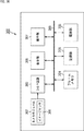
図36の撮像装置300は、カメラモジュール302、およびカメラ信号処理回路であるDSP(Digital Signal Processor)回路303を備える。また、撮像装置300は、フレームメモリ304、表示部305、記録部306、操作部307、および電源部308も備える。DSP回路303、フレームメモリ304、表示部305、記録部306、操作部307および電源部308は、バスライン309を介して相互に接続されている。
The
カメラモジュール302内のイメージセンサ301は、被写体からの入射光(像光)を取り込んで撮像面上に結像された入射光の光量を画素単位で電気信号に変換して画素信号として出力する。このカメラモジュール302として、カメラモジュール151または複眼カメラモジュール201が採用されており、イメージセンサ301は、図1のイメージセンサ11に対応する。なお、カメラモジュール302に代えて、上述した各実施の形態のイメージセンサパッケージ1と、任意のレンズ構造体を組み合わせた構成を採用してもよい。
The
表示部305は、例えば、液晶パネルや有機EL(Electro Luminescence)パネル等のパネル型表示装置からなり、イメージセンサ301で撮像された動画または静止画を表示する。記録部306は、イメージセンサ301で撮像された動画または静止画を、ハードディスクや半導体メモリ等の記録媒体に記録する。
The
操作部307は、ユーザによる操作の下に、撮像装置300が持つ様々な機能について操作指令を発する。電源部308は、DSP回路303、フレームメモリ304、表示部305、記録部306および操作部307の動作電源となる各種の電源を、これら供給対象に対して適宜供給する。
The
上述したように、カメラモジュール302として、イメージセンサ11のI/O数の増加に対応したイメージセンサパッケージ1を用いることで、高画質化及び小型化を実現することができる。また、イメージセンサ11またはガラス基板23の側面を覆う被覆部24が形成されたイメージセンサパッケージ1を用いることで、意図しない光がイメージセンサ11の受光部に入射することを防止するとともに、イメージセンサ11から発生する熱を放散するための放熱経路を形成することができる。
As described above, by using the
従って、ビデオカメラやデジタルスチルカメラ、さらには携帯電話機等のモバイル機器向けカメラモジュールなどの撮像装置300においても、半導体パッケージの小型化と、撮像画像の高画質化の両立を図ることができる。
Therefore, in the
<イメージセンサの使用例>
図37は、イメージセンサパッケージ1、カメラモジュール151、または複眼カメラモジュール201として構成されたイメージセンサの使用例を示す図である。<Example of using image sensor>
FIG. 37 is a diagram showing a usage example of an image sensor configured as an
イメージセンサパッケージ1、カメラモジュール151、または複眼カメラモジュール201として構成されたイメージセンサは、例えば、以下のように、可視光や、赤外光、紫外光、X線等の光をセンシングする様々なケースに使用することができる。
The image sensor configured as the
・デジタルカメラや、カメラ機能付きの携帯機器等の、鑑賞の用に供される画像を撮影する装置
・自動停止等の安全運転や、運転者の状態の認識等のために、自動車の前方や後方、周囲、車内等を撮影する車載用センサ、走行車両や道路を監視する監視カメラ、車両間等の測距を行う測距センサ等の、交通の用に供される装置
・ユーザのジェスチャを撮影して、そのジェスチャに従った機器操作を行うために、TVや、冷蔵庫、エアーコンディショナ等の家電に供される装置
・内視鏡や、赤外光の受光による血管撮影を行う装置等の、医療やヘルスケアの用に供される装置
・防犯用途の監視カメラや、人物認証用途のカメラ等の、セキュリティの用に供される装置
・肌を撮影する肌測定器や、頭皮を撮影するマイクロスコープ等の、美容の用に供される装置
・スポーツ用途等向けのアクションカメラやウェアラブルカメラ等の、スポーツの用に供される装置
・畑や作物の状態を監視するためのカメラ等の、農業の用に供される装置・ Devices that take images for viewing, such as digital cameras and portable devices with camera functions. ・ For safe driving such as automatic stop and recognition of the driver's condition, in front of the car Devices used for traffic, such as in-vehicle sensors that photograph the rear, surroundings, and interior of vehicles, surveillance cameras that monitor traveling vehicles and roads, and distance measurement sensors that measure distance between vehicles, etc. Equipment used in home appliances such as TVs, refrigerators, and air conditioners to take pictures and operate the equipment according to the gestures ・ Endoscopes, devices that perform angiography by receiving infrared light, etc. Equipment used for medical and healthcare ・ Equipment used for security such as surveillance cameras for crime prevention and cameras for person authentication ・ Skin measuring instruments for taking pictures of the skin and taking pictures of the scalp Equipment used for beauty such as microscopes ・ Equipment used for sports such as action cameras and wearable cameras for sports applications ・ Camera etc. for monitoring the condition of fields and crops , Equipment used for agriculture
本技術の実施の形態は、上述した実施の形態に限定されるものではなく、本技術の要旨を逸脱しない範囲において種々の変更が可能である。 The embodiment of the present technology is not limited to the above-described embodiment, and various changes can be made without departing from the gist of the present technology.
例えば、本技術は、可視光の入射光量の分布を検知して画像として撮像する固体撮像装置への適用に限らず、赤外線やX線、あるいは粒子等の入射量の分布を画像として撮像する固体撮像装置や、広義の意味として、圧力や静電容量など、他の物理量の分布を検知して画像として撮像する指紋検出センサ等の固体撮像装置(物理量分布検知装置)全般に対して適用可能である。 For example, this technology is not limited to application to a solid-state image sensor that detects the distribution of the incident light amount of visible light and captures it as an image, but is also a solid that captures the distribution of the incident amount of infrared rays, X-rays, particles, etc. as an image. It can be applied to image sensors and, in a broad sense, all solid-state image sensors (physical quantity distribution detection devices) such as fingerprint detection sensors that detect the distribution of other physical quantities such as pressure and capacitance and capture images as images. is there.
例えば、上述した複数の実施の形態の全てまたは一部を組み合わせた形態を採用することができる。 For example, a form in which all or a part of the plurality of embodiments described above can be combined can be adopted.
なお、本明細書に記載された効果はあくまで例示であって限定されるものではなく、本明細書に記載されたもの以外の効果があってもよい。 It should be noted that the effects described in the present specification are merely examples and are not limited, and effects other than those described in the present specification may be obtained.
なお、本技術は以下のような構成も取ることができる。
(1)
半導体基板に光電変換素子が形成されたイメージセンサと、
前記イメージセンサの第1の主面側に配置されたガラス基板と、
前記イメージセンサの前記第1の主面と反対側の第2の主面側に形成された第1配線層と、
前記イメージセンサの信号を外部に出力する外部端子と
を備え、
前記第1配線層の金属配線は、前記イメージセンサの内部から外周部へ拡がるように形成されて前記外部端子と接続されている
半導体装置。
(2)
半導体基板に光電変換素子が形成されたイメージセンサと、
前記イメージセンサの受光面である第1の主面を保護するガラス基板と、
前記イメージセンサと前記ガラス基板の側面を覆う絶縁性部材と
を備える半導体装置。
(3)
前記第1配線層が形成されている平面領域は、前記イメージセンサの平面領域よりも大きい
前記(1)または(2)に記載の半導体装置。
(4)
前記ガラス基板と前記第1配線層との間であって、前記イメージセンサの側面は、絶縁性材料で覆われている
前記(1)乃至(3)のいずれかに記載の半導体装置。
(5)
前記絶縁性材料は、遮光性の材料と高熱伝導性を有する材料の2種類の絶縁性材料を含む
前記(4)に記載の半導体装置。
(6)
前記イメージセンサの第1の主面と前記ガラス基板との間に、第2配線層が挿入されている
前記(1)乃至(5)のいずれかに記載の半導体装置。
(7)
前記ガラス基板の側面は、絶縁性材料で覆われている
前記(1)乃至(6)のいずれかに記載の半導体装置。
(8)
前記イメージセンサの第1の主面と前記ガラス基板との間に、光透過性部材が封入されている
前記(1)乃至(7)のいずれかに記載の半導体装置。
(9)
前記イメージセンサの第1の主面と前記ガラス基板との間に、空気が封入されている
前記(1)乃至(8)のいずれかに記載の半導体装置。
(10)
前記イメージセンサの前記第2の主面と前記第1配線層との間に、1種類以上の絶縁性材料が挿入されている
前記(1)、(3)乃至(9)のいずれかに記載の半導体装置。
(11)
前記イメージセンサの前記第2の主面の電極部と、前記第1配線層とが、金属バンプを介して電気的に接続されている
前記(10)に記載の半導体装置。
(12)
前記イメージセンサの前記第2の主面の電極部と、前記第1配線層とが、ビアを介して電気的に接続されている
前記(10)に記載の半導体装置。
(13)
前記ガラス基板の外周部は、その内側よりも厚く形成されている
前記(1)、(3)乃至(12)のいずれかに記載の半導体装置。
(14)
複数のレンズが積層されたレンズ構造体をさらに備え、
前記複数のレンズで集光された光が前記イメージセンサに入射されるように構成されている
前記(1)、(3)乃至(13)のいずれかに記載の半導体装置。
(15)
前記イメージセンサの前記第1の主面と反対側の第2の主面も、前記絶縁性部材で覆われている
前記(2)に記載の半導体装置。
(16)
半導体基板に光電変換素子が形成されたイメージセンサの第1の主面側にガラス基板を配置し、
前記イメージセンサの前記第1の主面と反対側の第2の主面側に、前記イメージセンサの内部から外周部へ拡がる金属配線を含む配線層を形成し、
前記金属配線と接続する前記外部端子を形成する
半導体装置の製造方法。
(17)
半導体基板に光電変換素子が形成されたイメージセンサと、
前記イメージセンサの第1の主面側に配置されたガラス基板と、
前記イメージセンサの前記第1の主面と反対側の第2の主面側に形成された配線層と、
前記イメージセンサの信号を外部に出力する外部端子と
を備え、
前記配線層の金属配線は、前記イメージセンサの内部から外周部へ拡がるように形成されて前記外部端子と接続されている
半導体装置
を備える電子機器。
(18)
半導体基板に光電変換素子が形成されたイメージセンサと、
前記イメージセンサの受光面を保護するガラス基板と、
前記イメージセンサと前記ガラス基板の側面を覆う絶縁性部材と
を備える半導体装置
を備える電子機器。The present technology can also have the following configurations.
(1)
An image sensor in which a photoelectric conversion element is formed on a semiconductor substrate,
A glass substrate arranged on the first main surface side of the image sensor and
A first wiring layer formed on the second main surface side opposite to the first main surface of the image sensor, and
It is equipped with an external terminal that outputs the signal of the image sensor to the outside.
The metal wiring of the first wiring layer is a semiconductor device formed so as to extend from the inside of the image sensor to the outer peripheral portion and connected to the external terminal.
(2)
An image sensor in which a photoelectric conversion element is formed on a semiconductor substrate,
A glass substrate that protects the first main surface, which is the light receiving surface of the image sensor, and
A semiconductor device including the image sensor and an insulating member that covers the side surface of the glass substrate.
(3)
The semiconductor device according to (1) or (2), wherein the plane region on which the first wiring layer is formed is larger than the plane region of the image sensor.
(4)
The semiconductor device according to any one of (1) to (3), wherein the side surface of the image sensor is covered with an insulating material between the glass substrate and the first wiring layer.
(5)
The semiconductor device according to (4) above, wherein the insulating material includes two types of insulating materials, a light-shielding material and a material having high thermal conductivity.
(6)
The semiconductor device according to any one of (1) to (5) above, wherein a second wiring layer is inserted between the first main surface of the image sensor and the glass substrate.
(7)
The semiconductor device according to any one of (1) to (6) above, wherein the side surface of the glass substrate is covered with an insulating material.
(8)
The semiconductor device according to any one of (1) to (7) above, wherein a light transmissive member is enclosed between the first main surface of the image sensor and the glass substrate.
(9)
The semiconductor device according to any one of (1) to (8) above, wherein air is sealed between the first main surface of the image sensor and the glass substrate.
(10)
The above (1), (3) to (9), wherein one or more kinds of insulating materials are inserted between the second main surface of the image sensor and the first wiring layer. Semiconductor device.
(11)
The semiconductor device according to (10), wherein the electrode portion of the second main surface of the image sensor and the first wiring layer are electrically connected via metal bumps.
(12)
The semiconductor device according to (10), wherein the electrode portion of the second main surface of the image sensor and the first wiring layer are electrically connected via vias.
(13)
The semiconductor device according to any one of (1), (3) to (12), wherein the outer peripheral portion of the glass substrate is formed thicker than the inside thereof.
(14)
Further provided with a lens structure in which multiple lenses are laminated,
The semiconductor device according to any one of (1), (3) to (13), wherein the light collected by the plurality of lenses is incident on the image sensor.
(15)
The semiconductor device according to (2), wherein the second main surface of the image sensor opposite to the first main surface is also covered with the insulating member.
(16)
A glass substrate is placed on the first main surface side of the image sensor in which the photoelectric conversion element is formed on the semiconductor substrate.
A wiring layer including metal wiring extending from the inside to the outer peripheral portion of the image sensor is formed on the second main surface side opposite to the first main surface of the image sensor.
A method for manufacturing a semiconductor device that forms the external terminal to be connected to the metal wiring.
(17)
An image sensor in which a photoelectric conversion element is formed on a semiconductor substrate,
A glass substrate arranged on the first main surface side of the image sensor and
A wiring layer formed on the second main surface side opposite to the first main surface of the image sensor, and
It is equipped with an external terminal that outputs the signal of the image sensor to the outside.
The metal wiring of the wiring layer is an electronic device including a semiconductor device formed so as to extend from the inside of the image sensor to the outer peripheral portion and connected to the external terminal.
(18)
An image sensor in which a photoelectric conversion element is formed on a semiconductor substrate,
A glass substrate that protects the light receiving surface of the image sensor and
An electronic device including a semiconductor device including the image sensor and an insulating member that covers the side surface of the glass substrate.
1 イメージセンサパッケージ, 11 イメージセンサ, 12 第1の主面, 13 第2の主面, 21 オンチップレンズ, 22 光透過性部材, 23 ガラス基板, 24,24A,24B 被覆部, 31 再配線層, 32 金属配線層, 33 絶縁層, 34 外部端子, 41 金属バンプ, 55 被覆部, 56 ビア, 61 金属配線層, 62 絶縁層, 63 配線層, 121,122 チップ部品, 151 カメラモジュール, 171 レンズ, 173 レンズ構造体, 201 複眼カメラモジュール, 212 湾曲部, 300 撮像装置, 301 イメージセンサ, 302 カメラモジュール 1 image sensor package, 11 image sensor, 12 first main surface, 13 second main surface, 21 on-chip lens, 22 light transmissive member, 23 glass substrate, 24, 24A, 24B coating, 31 rewiring layer , 32 Metal wiring layer, 33 Insulation layer, 34 External terminal, 41 Metal bump, 55 Coating part, 56 Via, 61 Metal wiring layer, 62 Insulation layer, 63 Wiring layer, 121, 122 Chip parts, 151 Camera module, 171 lens , 173 lens structure, 201 compound eye camera module, 212 curved part, 300 image pickup device, 301 image sensor, 302 camera module
Claims (17)
前記イメージセンサの第1の主面側に配置されたガラス基板と、
複数の金属配線層と、その間に形成された絶縁層とを含み、前記イメージセンサの前記第1の主面と反対側の第2の主面側に形成された第1配線層と、
複数の金属配線層と、その間に形成された絶縁層とを含み、前記イメージセンサの第1の主面と前記ガラス基板との間に挿入された第2配線層と、
前記イメージセンサの信号を外部に出力する外部端子と
を備え、
前記第1配線層の最下層の金属配線層は、前記イメージセンサの内部から外周部へ拡がるように形成されて前記外部端子と接続され、
前記第2配線層は、平面視で前記イメージセンサの受光部より外側に配置され、
前記第2配線層の少なくとも1つの金属配線層は、前記イメージセンサの前記第1の主面上の周縁部で前記イメージセンサと電気的に接続されている
半導体装置。 An image sensor in which a photoelectric conversion element is formed on a semiconductor substrate,
A glass substrate arranged on the first main surface side of the image sensor and
A first wiring layer including a plurality of metal wiring layers and an insulating layer formed between them, and formed on a second main surface side opposite to the first main surface of the image sensor.
A second wiring layer that includes a plurality of metal wiring layers and an insulating layer formed between them, and is inserted between the first main surface of the image sensor and the glass substrate.
It is equipped with an external terminal that outputs the signal of the image sensor to the outside.
The lowermost metal wiring layer of the first wiring layer, said from the interior of the image sensor is formed so as to extend to the outer peripheral portion connected to said external terminal,
The second wiring layer is arranged outside the light receiving portion of the image sensor in a plan view.
A semiconductor device in which at least one metal wiring layer of the second wiring layer is electrically connected to the image sensor at a peripheral edge portion on the first main surface of the image sensor.
請求項1に記載の半導体装置。 The semiconductor device according to claim 1, wherein the plane region on which the first wiring layer is formed is larger than the plane region of the image sensor.
請求項1または2に記載の半導体装置。 The semiconductor device according to claim 1 or 2, wherein the side surface of the image sensor is covered with an insulating material between the glass substrate and the first wiring layer.
請求項3に記載の半導体装置。 The semiconductor device according to claim 3, wherein the insulating material includes two types of insulating materials, a light-shielding material and a material having high thermal conductivity.
請求項1乃至4のいずれかに記載の半導体装置。 Wherein the at least one metal wiring layer of the second wiring layer, the semiconductor device according to the the first major surface of the image sensor, any one of claims 1 to 4 are electrically connected via the metal member ..
請求項5に記載の半導体装置。 The semiconductor device according to claim 5 , wherein the metal member is a metal bump.
請求項1乃至6のいずれかに記載の半導体装置。 The semiconductor device according to any one of claims 1 to 6 , wherein the side surface of the glass substrate is covered with an insulating material.
請求項1乃至7のいずれかに記載の半導体装置。 The semiconductor device according to any one of claims 1 to 7 , wherein a light transmissive member is enclosed between the light receiving portion of the image sensor and the glass substrate.
請求項1乃至7のいずれかに記載の半導体装置。 The semiconductor device according to any one of claims 1 to 7, wherein air is sealed between the light receiving portion of the image sensor and the glass substrate.
請求項1乃至8のいずれかに記載の半導体装置。 The semiconductor device according to any one of claims 1 to 8, wherein one or more kinds of insulating materials are inserted between the second main surface of the image sensor and the first wiring layer.
請求項10に記載の半導体装置。 The semiconductor device according to claim 10 , wherein the electrode portion of the second main surface of the image sensor and the predetermined metal wiring layer of the first wiring layer are electrically connected via metal bumps. ..
請求項10に記載の半導体装置。 The semiconductor device according to claim 10 , wherein the electrode portion of the second main surface of the image sensor and the predetermined metal wiring layer of the first wiring layer are electrically connected via vias.
前記複数のレンズで集光された光が前記イメージセンサに入射されるように構成されている
請求項1乃至12のいずれかに記載の半導体装置。 Further provided with a lens structure in which multiple lenses are laminated,
The semiconductor device according to any one of claims 1 to 12, wherein the light collected by the plurality of lenses is incident on the image sensor.
請求項1乃至13のいずれかに記載の半導体装置。 The semiconductor device according to any one of claims 1 to 13, wherein the side surface of the second wiring layer is covered with an insulating material.
請求項1に記載の半導体装置。 The semiconductor device according to claim 1, wherein the surface of the second wiring layer opposite to the surface connected to the image sensor is connected to the glass substrate.
前記イメージセンサの前記第1の主面と反対側の第2の主面側に、複数の金属配線層と、その間に形成された絶縁層とを含む第1配線層を形成し、
前記イメージセンサの第1の主面と前記ガラス基板との間に、複数の金属配線層と、その間に形成された絶縁層とを含む第2配線層を形成し、
前記イメージセンサの信号を外部に出力する外部端子を形成し、
前記第2配線層は、平面視で前記イメージセンサの受光部より外側に配置され、
前記第2配線層の少なくとも1つの金属配線層は、前記イメージセンサの前記第1の主面上の周縁部で前記イメージセンサと電気的に接続され、
前記第1配線層の最下層の金属配線層は、前記イメージセンサの内部から外周部へ拡がるように形成されて前記外部端子と接続される
半導体装置の製造方法。 A glass substrate is placed on the first main surface side of the image sensor in which the photoelectric conversion element is formed on the semiconductor substrate.
A first wiring layer including a plurality of metal wiring layers and an insulating layer formed between them is formed on the second main surface side opposite to the first main surface of the image sensor.
A second wiring layer including a plurality of metal wiring layers and an insulating layer formed between them is formed between the first main surface of the image sensor and the glass substrate.
An external terminal that outputs the signal of the image sensor to the outside is formed.
The second wiring layer is arranged outside the light receiving portion of the image sensor in a plan view.
At least one metal wiring layer of the second wiring layer is electrically connected to the image sensor at a peripheral edge on the first main surface of the image sensor.
A method for manufacturing a semiconductor device in which the metal wiring layer of the lowermost layer of the first wiring layer is formed so as to extend from the inside of the image sensor to the outer peripheral portion and is connected to the external terminal.
前記イメージセンサの第1の主面側に配置されたガラス基板と、
複数の金属配線層と、その間に形成された絶縁層とを含み、前記イメージセンサの前記第1の主面と反対側の第2の主面側に形成された第1配線層と、
複数の金属配線層と、その間に形成された絶縁層とを含み、前記イメージセンサの第1の主面と前記ガラス基板との間に挿入された第2配線層と、
前記イメージセンサの信号を外部に出力する外部端子と
を備え、
前記第1配線層の最下層の金属配線層は、前記イメージセンサの内部から外周部へ拡がるように形成されて前記外部端子と接続され、
前記第2配線層は、平面視で前記イメージセンサの受光部より外側に配置され、
前記第2配線層の少なくとも1つの金属配線層は、前記イメージセンサの前記第1の主面上の周縁部で前記イメージセンサと電気的に接続されている
半導体装置
を備える電子機器。 An image sensor in which a photoelectric conversion element is formed on a semiconductor substrate,
A glass substrate arranged on the first main surface side of the image sensor and
A first wiring layer including a plurality of metal wiring layers and an insulating layer formed between them, and formed on a second main surface side opposite to the first main surface of the image sensor.
A second wiring layer that includes a plurality of metal wiring layers and an insulating layer formed between them, and is inserted between the first main surface of the image sensor and the glass substrate.
It is equipped with an external terminal that outputs the signal of the image sensor to the outside.
The lowermost metal wiring layer of the first wiring layer, said from the interior of the image sensor is formed so as to extend to the outer peripheral portion connected to said external terminal,
The second wiring layer is arranged outside the light receiving portion of the image sensor in a plan view.
An electronic device including a semiconductor device in which at least one metal wiring layer of the second wiring layer is electrically connected to the image sensor at a peripheral edge portion on the first main surface of the image sensor.
Applications Claiming Priority (3)
| Application Number | Priority Date | Filing Date | Title |
|---|---|---|---|
| JP2015145944 | 2015-07-23 | ||
| JP2015145944 | 2015-07-23 | ||
| PCT/JP2016/070262 WO2017014072A1 (en) | 2015-07-23 | 2016-07-08 | Semiconductor apparatus, method for manufacturing same, and electronic device |
Publications (2)
| Publication Number | Publication Date |
|---|---|
| JPWO2017014072A1 JPWO2017014072A1 (en) | 2018-05-10 |
| JP6885331B2 true JP6885331B2 (en) | 2021-06-16 |
Family
ID=57833908
Family Applications (1)
| Application Number | Title | Priority Date | Filing Date |
|---|---|---|---|
| JP2017529550A Expired - Fee Related JP6885331B2 (en) | 2015-07-23 | 2016-07-08 | Semiconductor devices, their manufacturing methods, and electronic devices |
Country Status (4)
| Country | Link |
|---|---|
| US (1) | US10763286B2 (en) |
| JP (1) | JP6885331B2 (en) |
| CN (1) | CN107851651B (en) |
| WO (1) | WO2017014072A1 (en) |
Families Citing this family (30)
| Publication number | Priority date | Publication date | Assignee | Title |
|---|---|---|---|---|
| CN106845436B (en) * | 2017-02-10 | 2020-06-02 | 京东方科技集团股份有限公司 | Fingerprint identification module, fingerprint identification method and touch screen |
| JP2019029979A (en) * | 2017-08-04 | 2019-02-21 | ソニーセミコンダクタソリューションズ株式会社 | Semiconductor device, electronic apparatus, and manufacturing method |
| JP2019066422A (en) * | 2017-10-04 | 2019-04-25 | ソニーセミコンダクタソリューションズ株式会社 | Inspection device, inspection method, and program |
| JP2019216187A (en) * | 2018-06-13 | 2019-12-19 | ソニーセミコンダクタソリューションズ株式会社 | Imaging apparatus |
| JP6596551B1 (en) * | 2018-09-06 | 2019-10-23 | 株式会社フジクラ | Electronic component unit |
| US11329083B2 (en) * | 2018-09-26 | 2022-05-10 | Taiwan Semiconductor Manufacturing Company, Ltd. | Wafer level image sensor package |
| CN112753215B (en) * | 2018-10-15 | 2024-04-19 | 索尼半导体解决方案公司 | Solid-state image pickup device and electronic apparatus |
| US10903255B2 (en) * | 2018-11-08 | 2021-01-26 | Semiconductor Components Industries, Llc | Image sensor flip chip package |
| WO2020105119A1 (en) | 2018-11-20 | 2020-05-28 | オリンパス株式会社 | Endoscopic imaging device and endoscope |
| WO2020183822A1 (en) | 2019-03-12 | 2020-09-17 | ソニーセミコンダクタソリューションズ株式会社 | Semiconductor package, and method for manufacturing semiconductor package |
| JP7449920B2 (en) * | 2019-03-12 | 2024-03-14 | ソニーセミコンダクタソリューションズ株式会社 | semiconductor equipment |
| CN111866322A (en) * | 2019-04-30 | 2020-10-30 | 宁波舜宇光电信息有限公司 | Camera module and its photosensitive assembly, electronic equipment and preparation method |
| JP2020198374A (en) * | 2019-06-04 | 2020-12-10 | ソニーセミコンダクタソリューションズ株式会社 | Image capture device |
| JP7234816B2 (en) * | 2019-06-11 | 2023-03-08 | 株式会社デンソー | rangefinder |
| JP7499242B2 (en) * | 2019-06-28 | 2024-06-13 | ソニーセミコンダクタソリューションズ株式会社 | Semiconductor package and electronic device |
| US12010416B1 (en) * | 2019-09-27 | 2024-06-11 | Apple Inc. | Camera module including embedded ceramic substrate package |
| CN111029354B (en) * | 2019-12-03 | 2024-02-27 | 西安电子科技大学 | A three-dimensional integrated circuit structure for a large area array, high frame rate, high reliability and miniaturized image sensor |
| US12356753B2 (en) * | 2019-12-04 | 2025-07-08 | Sony Semiconductor Solutions Corporation | Imaging device and method for manufacturing imaging device |
| TWI721837B (en) * | 2020-03-26 | 2021-03-11 | 勝麗國際股份有限公司 | Sensor package structure |
| TWI747218B (en) * | 2020-03-27 | 2021-11-21 | 勝麗國際股份有限公司 | Chip-scale sensor package structure |
| WO2021224996A1 (en) * | 2020-05-08 | 2021-11-11 | オリンパス株式会社 | Imaging module, endoscopic system, and method for manufacturing imaging module |
| WO2021261234A1 (en) * | 2020-06-22 | 2021-12-30 | ソニーセミコンダクタソリューションズ株式会社 | Solid-state imaging device, method for manufacturing same, and electronic apparatus |
| JP2024123285A (en) * | 2021-07-21 | 2024-09-11 | ソニーセミコンダクタソリューションズ株式会社 | Semiconductor Package |
| WO2023053503A1 (en) * | 2021-09-30 | 2023-04-06 | ソニーセミコンダクタソリューションズ株式会社 | Imaging device, electronic apparatus, and method for manufacturing imaging device |
| US11798967B2 (en) * | 2021-10-06 | 2023-10-24 | Stmicroelectronics Asia Pacific Pte Ltd | Image sensor package with transparent adhesive covering the optical sensing circuit |
| US12035060B2 (en) * | 2021-11-05 | 2024-07-09 | Omnivision Technologies, Inc. | Stacked image sensor |
| US12228776B2 (en) | 2022-01-31 | 2025-02-18 | Taiwan Semiconductor Manufacturing Co., Ltd. | Package with integrated optical die and method forming same |
| WO2024014134A1 (en) * | 2022-07-14 | 2024-01-18 | ソニーセミコンダクタソリューションズ株式会社 | Solid-state imaging device |
| CN120677562A (en) * | 2023-02-27 | 2025-09-19 | 索尼半导体解决方案公司 | Semiconductor device, electronic apparatus, and method for producing semiconductor device |
| US20250393328A1 (en) * | 2024-06-19 | 2025-12-25 | Semiconductor Components Industries, Llc | Sensor fan-out packaging |
Family Cites Families (16)
| Publication number | Priority date | Publication date | Assignee | Title |
|---|---|---|---|---|
| JP5030360B2 (en) * | 2002-12-25 | 2012-09-19 | オリンパス株式会社 | Method for manufacturing solid-state imaging device |
| KR100498708B1 (en) | 2004-11-08 | 2005-07-01 | 옵토팩 주식회사 | Electronic package for semiconductor device and packaging method thereof |
| JP2008130738A (en) * | 2006-11-20 | 2008-06-05 | Fujifilm Corp | Solid-state image sensor |
| JP5123575B2 (en) * | 2007-06-14 | 2013-01-23 | 株式会社フジクラ | Wiring board and manufacturing method thereof |
| JP4693827B2 (en) | 2007-09-20 | 2011-06-01 | 株式会社東芝 | Semiconductor device and manufacturing method thereof |
| JP5005603B2 (en) * | 2008-04-03 | 2012-08-22 | 新光電気工業株式会社 | Semiconductor device and manufacturing method thereof |
| JP5438980B2 (en) * | 2009-01-23 | 2014-03-12 | ラピスセミコンダクタ株式会社 | Manufacturing method of semiconductor device |
| TWI437700B (en) * | 2010-05-31 | 2014-05-11 | 勝開科技股份有限公司 | Method for manufacturing wafer level image sensor structure |
| US9252172B2 (en) * | 2011-05-31 | 2016-02-02 | Stats Chippac, Ltd. | Semiconductor device and method of forming EWLB semiconductor package with vertical interconnect structure and cavity region |
| JP2013041878A (en) | 2011-08-11 | 2013-02-28 | Sony Corp | Imaging apparatus and camera module |
| JP6146976B2 (en) | 2012-09-24 | 2017-06-14 | オリンパス株式会社 | Imaging device and endoscope provided with the imaging device |
| US9172408B2 (en) * | 2012-09-27 | 2015-10-27 | Mediatek Inc. | Transmitter supporting two modes |
| KR102256719B1 (en) * | 2014-05-12 | 2021-05-28 | 삼성전자주식회사 | semiconductor package and method for manufacturing of the same |
| JP6230520B2 (en) * | 2014-10-29 | 2017-11-15 | キヤノン株式会社 | Printed circuit board and electronic device |
| FR3029687A1 (en) * | 2014-12-09 | 2016-06-10 | Stmicroelectronics (Grenoble 2) Sas | METHOD FOR MANUFACTURING ELECTRONIC DEVICES AND ELECTRONIC DEVICE WITH DOUBLE ENCAPSULATION RING |
| US9899442B2 (en) * | 2014-12-11 | 2018-02-20 | Invensas Corporation | Image sensor device |
-
2016
- 2016-07-08 JP JP2017529550A patent/JP6885331B2/en not_active Expired - Fee Related
- 2016-07-08 CN CN201680041625.XA patent/CN107851651B/en not_active Expired - Fee Related
- 2016-07-08 WO PCT/JP2016/070262 patent/WO2017014072A1/en not_active Ceased
- 2016-07-08 US US15/745,176 patent/US10763286B2/en active Active
Also Published As
| Publication number | Publication date |
|---|---|
| CN107851651B (en) | 2022-07-08 |
| JPWO2017014072A1 (en) | 2018-05-10 |
| CN107851651A (en) | 2018-03-27 |
| US20180211989A1 (en) | 2018-07-26 |
| US10763286B2 (en) | 2020-09-01 |
| WO2017014072A1 (en) | 2017-01-26 |
Similar Documents
| Publication | Publication Date | Title |
|---|---|---|
| JP6885331B2 (en) | Semiconductor devices, their manufacturing methods, and electronic devices | |
| US11619772B2 (en) | Semiconductor chip and electronic apparatus | |
| US11437423B2 (en) | Image sensor, manufacturing method, and electronic device | |
| US11043436B2 (en) | Semiconductor device, manufacturing method, imaging device, and electronic apparatus for enabling component mounting with high flatness | |
| TWI377667B (en) | Module for optical apparatus and method of producing module for optical apparatus | |
| US11924557B2 (en) | Pinhole camera, electronic apparatus and manufacturing method | |
| CN108701696B (en) | Glass interposer module, imaging device and electronic device | |
| JP6743035B2 (en) | Imaging device and manufacturing method | |
| WO2004107738A1 (en) | Imaging device and its manufacturing method | |
| US9647146B2 (en) | Semiconductor device, manufacturing method, and electronic apparatus | |
| US20190221602A1 (en) | Solid state imaging device, solid state imaging device manufacturing method, and electronic apparatus | |
| JP2010045082A (en) | Display element/electronic element module and its manufacturing method, and electronic information equipment | |
| JP2013125881A (en) | Method of manufacturing solid-state imaging device | |
| US20180226442A1 (en) | Image sensor and manufacturing method thereof | |
| JP2016076616A (en) | Semiconductor device, manufacturing apparatus, manufacturing method | |
| JP2004296687A (en) | Imaging device, method of manufacturing the same, imaging module, and electronic device |
Legal Events
| Date | Code | Title | Description |
|---|---|---|---|
| A521 | Request for written amendment filed |
Free format text: JAPANESE INTERMEDIATE CODE: A523 Effective date: 20190621 |
|
| A621 | Written request for application examination |
Free format text: JAPANESE INTERMEDIATE CODE: A621 Effective date: 20190621 |
|
| A131 | Notification of reasons for refusal |
Free format text: JAPANESE INTERMEDIATE CODE: A131 Effective date: 20200512 |
|
| A521 | Request for written amendment filed |
Free format text: JAPANESE INTERMEDIATE CODE: A523 Effective date: 20200615 |
|
| A131 | Notification of reasons for refusal |
Free format text: JAPANESE INTERMEDIATE CODE: A131 Effective date: 20201201 |
|
| A521 | Request for written amendment filed |
Free format text: JAPANESE INTERMEDIATE CODE: A523 Effective date: 20210114 |
|
| TRDD | Decision of grant or rejection written | ||
| A01 | Written decision to grant a patent or to grant a registration (utility model) |
Free format text: JAPANESE INTERMEDIATE CODE: A01 Effective date: 20210413 |
|
| A61 | First payment of annual fees (during grant procedure) |
Free format text: JAPANESE INTERMEDIATE CODE: A61 Effective date: 20210426 |
|
| R151 | Written notification of patent or utility model registration |
Ref document number: 6885331 Country of ref document: JP Free format text: JAPANESE INTERMEDIATE CODE: R151 |
|
| LAPS | Cancellation because of no payment of annual fees |