WO2017057581A1 - p型4H-SiC単結晶及びp型4H-SiC単結晶の製造方法 - Google Patents
p型4H-SiC単結晶及びp型4H-SiC単結晶の製造方法 Download PDFInfo
- Publication number
- WO2017057581A1 WO2017057581A1 PCT/JP2016/078834 JP2016078834W WO2017057581A1 WO 2017057581 A1 WO2017057581 A1 WO 2017057581A1 JP 2016078834 W JP2016078834 W JP 2016078834W WO 2017057581 A1 WO2017057581 A1 WO 2017057581A1
- Authority
- WO
- WIPO (PCT)
- Prior art keywords
- single crystal
- sic single
- type
- sic
- aluminum
- Prior art date
- Legal status (The legal status is an assumption and is not a legal conclusion. Google has not performed a legal analysis and makes no representation as to the accuracy of the status listed.)
- Ceased
Links
Images
Classifications
-
- C—CHEMISTRY; METALLURGY
- C30—CRYSTAL GROWTH
- C30B—SINGLE-CRYSTAL GROWTH; UNIDIRECTIONAL SOLIDIFICATION OF EUTECTIC MATERIAL OR UNIDIRECTIONAL DEMIXING OF EUTECTOID MATERIAL; REFINING BY ZONE-MELTING OF MATERIAL; PRODUCTION OF A HOMOGENEOUS POLYCRYSTALLINE MATERIAL WITH DEFINED STRUCTURE; SINGLE CRYSTALS OR HOMOGENEOUS POLYCRYSTALLINE MATERIAL WITH DEFINED STRUCTURE; AFTER-TREATMENT OF SINGLE CRYSTALS OR A HOMOGENEOUS POLYCRYSTALLINE MATERIAL WITH DEFINED STRUCTURE; APPARATUS THEREFOR
- C30B23/00—Single-crystal growth by condensing evaporated or sublimed materials
- C30B23/02—Epitaxial-layer growth
- C30B23/06—Heating of the deposition chamber, the substrate or the materials to be evaporated
-
- C—CHEMISTRY; METALLURGY
- C30—CRYSTAL GROWTH
- C30B—SINGLE-CRYSTAL GROWTH; UNIDIRECTIONAL SOLIDIFICATION OF EUTECTIC MATERIAL OR UNIDIRECTIONAL DEMIXING OF EUTECTOID MATERIAL; REFINING BY ZONE-MELTING OF MATERIAL; PRODUCTION OF A HOMOGENEOUS POLYCRYSTALLINE MATERIAL WITH DEFINED STRUCTURE; SINGLE CRYSTALS OR HOMOGENEOUS POLYCRYSTALLINE MATERIAL WITH DEFINED STRUCTURE; AFTER-TREATMENT OF SINGLE CRYSTALS OR A HOMOGENEOUS POLYCRYSTALLINE MATERIAL WITH DEFINED STRUCTURE; APPARATUS THEREFOR
- C30B23/00—Single-crystal growth by condensing evaporated or sublimed materials
- C30B23/002—Controlling or regulating
-
- C—CHEMISTRY; METALLURGY
- C30—CRYSTAL GROWTH
- C30B—SINGLE-CRYSTAL GROWTH; UNIDIRECTIONAL SOLIDIFICATION OF EUTECTIC MATERIAL OR UNIDIRECTIONAL DEMIXING OF EUTECTOID MATERIAL; REFINING BY ZONE-MELTING OF MATERIAL; PRODUCTION OF A HOMOGENEOUS POLYCRYSTALLINE MATERIAL WITH DEFINED STRUCTURE; SINGLE CRYSTALS OR HOMOGENEOUS POLYCRYSTALLINE MATERIAL WITH DEFINED STRUCTURE; AFTER-TREATMENT OF SINGLE CRYSTALS OR A HOMOGENEOUS POLYCRYSTALLINE MATERIAL WITH DEFINED STRUCTURE; APPARATUS THEREFOR
- C30B29/00—Single crystals or homogeneous polycrystalline material with defined structure characterised by the material or by their shape
- C30B29/10—Inorganic compounds or compositions
- C30B29/36—Carbides
-
- H—ELECTRICITY
- H01—ELECTRIC ELEMENTS
- H01B—CABLES; CONDUCTORS; INSULATORS; SELECTION OF MATERIALS FOR THEIR CONDUCTIVE, INSULATING OR DIELECTRIC PROPERTIES
- H01B1/00—Conductors or conductive bodies characterised by the conductive materials; Selection of materials as conductors
- H01B1/04—Conductors or conductive bodies characterised by the conductive materials; Selection of materials as conductors mainly consisting of carbon-silicon compounds, carbon or silicon
-
- H—ELECTRICITY
- H10—SEMICONDUCTOR DEVICES; ELECTRIC SOLID-STATE DEVICES NOT OTHERWISE PROVIDED FOR
- H10P—GENERIC PROCESSES OR APPARATUS FOR THE MANUFACTURE OR TREATMENT OF DEVICES COVERED BY CLASS H10
- H10P14/00—Formation of materials, e.g. in the shape of layers or pillars
- H10P14/20—Formation of materials, e.g. in the shape of layers or pillars of semiconductor materials
- H10P14/24—Formation of materials, e.g. in the shape of layers or pillars of semiconductor materials using chemical vapour deposition [CVD]
-
- H—ELECTRICITY
- H10—SEMICONDUCTOR DEVICES; ELECTRIC SOLID-STATE DEVICES NOT OTHERWISE PROVIDED FOR
- H10P—GENERIC PROCESSES OR APPARATUS FOR THE MANUFACTURE OR TREATMENT OF DEVICES COVERED BY CLASS H10
- H10P14/00—Formation of materials, e.g. in the shape of layers or pillars
- H10P14/20—Formation of materials, e.g. in the shape of layers or pillars of semiconductor materials
- H10P14/32—Formation of materials, e.g. in the shape of layers or pillars of semiconductor materials characterised by intermediate layers between substrates and deposited layers
- H10P14/3202—Materials thereof
- H10P14/3204—Materials thereof being Group IVA semiconducting materials
- H10P14/3208—Silicon carbide
Definitions
- the present invention relates to a method for producing a p-type 4H—SiC single crystal and a p-type 4H—SiC single crystal.
- Silicon carbide (SiC) has a dielectric breakdown field that is an order of magnitude larger than silicon (Si) and a band gap that is three times larger. Silicon carbide (SiC) has characteristics such as about three times higher thermal conductivity than silicon (Si). Silicon carbide (SiC) is expected to be applied to power devices, high-frequency devices, high-temperature operation devices, and the like.
- 4H-SiC single crystal has high mobility and is expected to be used for power devices.
- Patent Document 1 describes that the specific resistance of an n-type 4H—SiC single crystal in which a donor element and an acceptor element are co-doped is small.
- a low-resistance p-type 4H-SiC single crystal occupies an important element in order to develop a SiC bipolar device having a high withstand voltage exceeding 10 kV, which is assumed to be used for power infrastructure.
- a low resistance p-type 4H—SiC single crystal is used as a substrate for manufacturing an n-channel SiC insulated gate bipolar transistor (IGBT) or the like.
- Non-Patent Document 1 describes that polymorphism in p-type 4H—SiC can be suppressed by co-doping aluminum and nitrogen.
- Non-Patent Document 1 the p-type 4H—SiC single crystal described in Non-Patent Document 1 cannot be said to have a sufficiently low specific resistance.
- the present invention has been made in view of the above problems, and an object thereof is to provide a p-type 4H—SiC single crystal having low resistance. Another object of the present invention is to provide a simple method for producing a low-resistance p-type 4H—SiC single crystal.
- the p-type 4H—SiC single crystal according to one embodiment of the present invention is doped with both aluminum and nitrogen, has a nitrogen concentration of 2.0 ⁇ 10 19 / cm 3 or more, and an aluminum concentration of 1.0 ⁇ 10 20 cm 3 or more.
- the aluminum concentration may be 1.8 ⁇ 10 20 / cm 3 or more.
- the p-type 4H—SiC single crystal described in either (1) or (2) may have a stacking fault density of 50 / cm or less.
- the p-type 4H—SiC single crystal described in any one of (1) to (3) above is any element of the group consisting of phosphorus, arsenic, titanium, vanadium, chromium, copper, iron, and nickel.
- the concentration of may be 2 ⁇ 10 15 / cm 3 or less.
- the p-type 4H—SiC single crystal according to any one of (1) to (4) may have a thickness of 1 mm or more.
- a method for producing a p-type 4H—SiC single crystal according to an aspect of the present invention includes a sublimation step of sublimating a nitrided aluminum raw material and a SiC raw material, and one side of the seed crystal is co-doped with aluminum and nitrogen. And a crystal growth step of stacking the SiC single crystals.
- the nitrided aluminum material and the SiC material are arranged separately, and are sublimated at different temperatures. You may let them.
- the sublimation step and the crystal growth step may be performed in a nitrogen gas atmosphere.
- the aluminum raw material is nitrided before the sublimation step, and the nitrided aluminum raw material is You may have the process to produce.
- the SiC single crystal according to one embodiment of the present invention is doped with nitrogen at a high concentration. As a result, a p-type 4H—SiC single crystal having a low specific resistance can be provided.
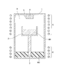
- FIG. 1 is a schematic cross-sectional view showing an example of a SiC single crystal manufacturing apparatus that can be used in a method for manufacturing a p-type 4H—SiC single crystal according to an aspect of the present invention.
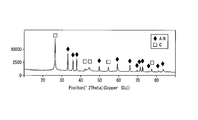
- the X-ray-diffraction result of the aluminum raw material after nitriding treatment is shown.
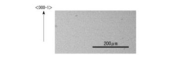
- the optical microscope image at the time of the cross-sectional observation of the SiC single crystal produced in Example 1 is shown.
- the p-type 4H—SiC single crystal is a p-type semiconductor in which aluminum and nitrogen are co-doped. Since it is a p-type semiconductor, carriers are holes generated by being doped with aluminum as an acceptor and being activated.
- the p-type 4H—SiC single crystal according to one embodiment of the present invention has a nitrogen concentration of 2.0 ⁇ 10 19 / cm 3 or more.
- the nitrogen concentration is preferably 1.0 ⁇ 10 20 / cm 3 or more, and more preferably 1.5 ⁇ 10 20 / cm 3 or more.
- a p-type 4H—SiC single crystal having a low resistance of 100 m ⁇ cm or less can be obtained.
- a SiC single crystal obtained by the sublimation method a p-type 4H—SiC single crystal having a low resistance of 100 m ⁇ cm or less has never been reported so far, and the p-type 4H—SiC single crystal according to one embodiment of the present invention has not been reported. The resistance value reached for the first time.
- the aluminum concentration of the p-type 4H—SiC single crystal is preferably 1.0 ⁇ 10 20 / cm 3 or more, more preferably 1.8 ⁇ 10 20 / cm 3 or more, and 2.0 ⁇ 10 20 / Cm 3 or more is more preferable.
- the aluminum concentration is high, the number of holes as carriers increases in the SiC single crystal, and the specific resistance of the SiC single crystal can be reduced.
- the aluminum concentration is preferably 3 ⁇ 10 21 / cm 3 or less.
- the crystal structure of the p-type 4H—SiC single crystal is 4H—SiC and has no other polymorphs.
- the SiC single crystal has polymorphs such as 3C—SiC, 4H—SiC, and 6H—SiC.
- Polymorphism is caused by the fact that the crystal structure of SiC is the same as the outermost surface structure when viewed from the c-axis direction ( ⁇ 000-1> direction). Therefore, when a crystal grows in the c-axis direction, a structural change tends to occur from a 4H—SiC structure to a different polymorph (heterogeneous polymorph).
- polymorphs can cause the crystallinity of the SiC single crystal to decrease and increase the specific resistance.
- polymorphs such as 6H—SiC
- the intended device cannot be manufactured in the first place. If the crystal structure of the p-type 4H—SiC single crystal is composed only of 4H—SiC, the crystallinity is high, the specific resistance can be reduced, and the device can be manufactured stably. Suppression of polymorphism can be performed by co-doping with aluminum and nitrogen as described above.
- the stacking fault density is preferably 50 / cm or less, and more preferably does not include stacking faults.
- the stacking fault is a defect formed in the direction of the basal plane of the SiC single crystal, and is a defect that may deteriorate the crystallinity and affect the operation of the device.
- disorder of the crystal structure is one of the causes.
- the stacking fault can be regarded as a locally generated polymorph.
- a disorder in the ⁇ 000-1> direction parallel to the growth direction is caused by a flank stacking fault or the like
- a disorder in the ⁇ 11-20> direction or the ⁇ 1-100> direction perpendicular to the growth direction is a Shockley type stacking. It is considered to be converted into a defect or the like.
- Stacking faults in the p-type 4H—SiC single crystal can be reduced by co-doping with aluminum and nitrogen. This is because the distortion of the crystal structure can be relaxed by co-doping with aluminum and nitrogen. If the stacking fault density in the p-type 4H—SiC single crystal is small, it is possible to reduce the number of regions having defects that affect the device in the SiC single crystal, and the yield and reliability of the device can be improved.
- the concentration of any element of the group consisting of phosphorus, arsenic, titanium, vanadium, chromium, copper, iron, and nickel is 2 ⁇ 10 15 / cm 3 or less. Preferably there is. Moreover, it is more preferable that these elements are below the detection limit of secondary ion mass spectrometry (SIMS).
- SIMS secondary ion mass spectrometry
- an additive element such as chromium, titanium, or copper is often added to a solvent in order to obtain a normal surface SiC single crystal.
- an SiC single crystal produced by a method such as a solution method may contain these elements as impurities, although only a little. These impurities cause a decrease in the crystallinity of the SiC single crystal and a defect after device processing.
- the p-type 4H—SiC single crystal according to one embodiment of the present invention can be manufactured by a sublimation method as described later. Therefore, these impurities and the like can be avoided from being taken into the SiC single crystal.
- the p-type 4H—SiC single crystal may be a single crystal ingot made of a bulk single crystal or an SiC wafer obtained by processing an SiC single crystal ingot into a wafer.
- a SiC wafer has a thickness of about several hundred ⁇ m.
- a SiC ingot is a bulk single crystal from which a plurality of SiC wafers can be cut, it has a thickness of 1 mm or more.
- a low-resistance p-type 4H—SiC single crystal can be obtained in either a single crystal ingot or a SiC wafer.
- a p-type 4H—SiC single crystal can also be obtained by epitaxial growth, but a p-type 4H—SiC single crystal having a growth thickness exceeding 1 mm is very difficult to produce by a method using epitaxial growth, and the productivity is high. bad.
- the p-type 4H—SiC single crystal according to one embodiment of the present invention can achieve a low resistance of a specific resistance of 100 m ⁇ cm or less. Therefore, application to various uses such as an n-channel SiC insulated gate bipolar transistor (IGBT) can be expected.
- IGBT n-channel SiC insulated gate bipolar transistor
- the p-type 4H—SiC single crystal according to one embodiment of the present invention has high crystallinity and does not have polymorphism. Therefore, low resistance can be realized and the reliability of the device can be improved.
- the p-type 4H—SiC single crystal according to one embodiment of the present invention has almost no stacking fault. Therefore, the occurrence of a killer defect or the like of the device can be reduced, and the device manufacturing yield, device reliability, and the like can be improved.
- a method for producing a p-type 4H—SiC single crystal according to an aspect of the present invention includes a sublimation step of sublimating a nitrided aluminum raw material and a SiC raw material, and a SiC single crystal in which aluminum and nitrogen are co-doped on one surface of a seed crystal.
- FIG. 1 is a schematic cross-sectional view showing an example of an SiC single crystal manufacturing apparatus that can be used in a method for manufacturing a p-type 4H—SiC single crystal according to an aspect of the present invention.
- the SiC single crystal manufacturing apparatus 10 includes a crucible 1 that forms a reaction space R, a holding unit 2 that can hold a SiC raw material M1, a support unit 3 that supports the holding unit 2, and an installation unit 4 that can install a seed crystal S. And a first heater 5 that heats the first region and a second heater 6 that heats the second region. At the bottom of the crucible 1, an aluminum raw material M2 can be installed.
- a method for manufacturing a p-type 4H—SiC single crystal according to an aspect of the present invention will be described using the SiC single crystal manufacturing apparatus 10 as an example.
- SiC raw material M1 and aluminum raw material M2 are prepared.
- SiC raw material M1 can use SiC powder etc. which are generally used widely.
- the aluminum raw material M2 may be either a nitrided aluminum compound or a non-nitrided aluminum compound. In the case of using an unnitrided aluminum compound, the aluminum raw material M2 is nitrided in the manufacturing process described later.
- the nitrided aluminum compound AlN, Al 5 C 3 N, or the like can be used.
- As the non-nitrided aluminum compound Al 4 C 3 or the like can be used.
- the SiC raw material M1 and the aluminum raw material M2 are separately installed.
- the SiC raw material M1 can be installed in the holding part 2 and the aluminum raw material M2 can be installed in the bottom part of the crucible 1.
- SiC raw material M1 and the aluminum raw material M2 are sublimated.
- SiC raw material M1 and aluminum raw material M2 are preferably sublimated at different temperatures.
- the vapor pressure of the SiC raw material M1 is lower than the vapor pressure of the aluminum raw material M2. For this reason, when the aluminum raw material M2 is heated under the condition that the normal SiC raw material M1 is sublimated, the sublimation rate of the aluminum raw material M2 is increased, which causes a problem in adjustment of the aluminum doping amount and SiC crystal growth.
- the temperature control of the SiC raw material M1 and the aluminum raw material M2 can be realized by the first heater 5 and the second heater 6.
- the first heater 5 is designed to heat the first region where the SiC raw material M1 in the crucible 1 exists
- the second heater 6 is designed to heat the second region where the aluminum raw material M2 in the crucible 1 exists.
- the temperature of SiC raw material M1 and aluminum raw material M2 can be controlled separately. More specifically, the temperature of the first heater 5 is set to about 2200 to 2500 ° C. at which the SiC raw material M1 can sublime, and the temperature of the second heater 6 is set to about 1700 to 2000 ° C. at which the aluminum raw material M2 can be sublimated. it can.
- the aluminum raw material M2 When the aluminum raw material M2 is not nitrided, it is preferable to nitride the aluminum raw material M2 before sublimation to produce a nitrided aluminum raw material. Nitriding of the aluminum raw material M2 can be performed by heating in a nitrogen atmosphere.
- the aluminum raw material M2 may be nitrided in another apparatus, or may be nitrided in the crucible 1 before the SiC raw material M1 is installed.
- the aluminum raw material M2 is intentionally nitrided during the sublimation process, the aluminum raw material M2 is installed in the crucible 1 without being nitrided, and the atmosphere in the crucible 1 is made an environment in which the aluminum raw material M2 is easily nitrided. Good. Specifically, measures such as making the inside of the reaction space R before the sublimation treatment an atmosphere consisting only of nitrogen or supplying nitrogen into the crucible 1 from the bottom side where the aluminum raw material M2 is installed are taken. Can do.
- the sublimated source gas reaches the seed crystal S installed in the installation unit 4, and the SiC single crystal grows.
- the crystal growth process proceeds naturally by sublimating the SiC raw material M1 and the aluminum raw material M2. Since the gas sublimated from the aluminum raw material M2 contains both aluminum and nitrogen, these elements are taken in during crystal growth. As a result, a p-type 4H—SiC single crystal doped with both aluminum and nitrogen can be obtained.
- the sublimation process is preferably performed in a nitrogen gas atmosphere.
- nitrogen gas atmosphere means that the gas supplied into the crucible is only nitrogen.
- the gas species existing in the atmosphere is only nitrogen except for the sublimation gas sublimated from the SiC raw material M1 and the aluminum raw material M2.
- the inside of the reaction space R a nitrogen gas atmosphere
- the nitriding of the aluminum raw material M2 can be promoted, and nitrogen doping into the SiC single crystal in which the crystal has grown can be performed. That is, by setting the reaction space R to a nitrogen gas atmosphere, nitrogen can be doped at a higher concentration in the p-type 4H—SiC single crystal in which the crystal grows. Even in Non-Patent Document 1, it has not been possible to dope nitrogen into the p-type 4H—SiC single crystal at a higher concentration.
- Nitrogen gas can be supplied into the reaction space R through the crucible 1.
- the crucible 1 has nitrogen gas permeability. Therefore, even if the crucible 1 is not provided with a gas supply unit, the atmosphere surrounding the crucible 1 is a nitrogen gas atmosphere, so that the gas atmosphere in the reaction space R can also be a nitrogen gas atmosphere.
- a p-type 4H—SiC single crystal obtained by nitriding an aluminum raw material or using a nitrided aluminum raw material is used. Nitrogen concentration can be increased. As a result, a p-type 4H—SiC single crystal having a low specific resistance can be easily produced.
- the method for producing a p-type 4H—SiC single crystal according to one embodiment of the present invention uses a sublimation method, even a SiC ingot having a thickness of several mm or more can be relatively easily produced. In the method using epitaxial growth, it is not realistic to produce a SiC ingot having a thickness of several mm or more, and the productivity is extremely poor. In addition, since the method for manufacturing a p-type 4H—SiC single crystal according to one embodiment of the present invention uses a sublimation method, it can be avoided that unnecessary impurities and the like are taken in unlike a solution method.
- Example 1 In Example 1, a p-type 4H—SiC single crystal was produced using an apparatus having the same configuration as the SiC single crystal growth apparatus shown in FIG. Hereinafter, a specific procedure will be described.
- Al 4 C 3 powder was prepared as an aluminum raw material.
- the prepared Al 4 C 3 powder was previously nitrided in the apparatus.
- the nitriding conditions were heating at 1800 ° C. for 110 hours in a gas atmosphere with a nitrogen concentration of 100%.
- FIG. 2 shows an X-ray diffraction result of the aluminum raw material after the nitriding treatment.
- the horizontal axis is an angle 2 ⁇ formed by incident X-rays and diffracted X-rays, and the vertical axis indicates intensity.
- the obtained diffraction line consists of a peak derived from C and a peak derived from AlN, and it can be seen that most of the aluminum raw material of Example 1 is changed to AlN. Moreover, when the same examination was performed on another sample, a peak derived from Al 5 C 3 N was sometimes observed. That is, it can be seen that most of the aluminum raw material after the nitriding treatment is nitrided to become AlN / Al 5 C 3 N.
- the obtained nitrided aluminum raw material and the SiC raw material made of SiC powder were separately installed in the crucible.
- the nitrogen gas concentration in the crucible was set to 5%.
- the aluminum raw material was heated to 1900 ° C.
- the SiC raw material was heated to 2300 ° C.
- Each raw material sublimated by heating to obtain a SiC single crystal.
- the treatment time was 30 hours, and the thickness of the obtained SiC single crystal was 2.7 mm.
- the obtained SiC single crystal was cut into a wafer having a thickness of 0.2 mm, and the specific resistance was measured.
- the Hall measurement by the van der Pauw method was used for the specific resistance measurement.
- the nitrogen concentration and the aluminum concentration were also measured.
- the nitrogen concentration and aluminum concentration were measured using secondary ion mass spectrometry (SIMS), and the crystal structure was measured by Raman measurement.
- SIMS secondary ion mass spectrometry
- the impurity concentration of the SiC single crystal obtained in Example 1 was also measured using secondary ion mass spectrometry (SIMS). The results are shown in Table 1.
- Vanadium and titanium were detected, but other elements were below the SIMS detection limit and were not detected. Further, the detected vanadium and titanium concentrations are low, which is equivalent to a commercially available SiC wafer.
- FIG. 3 shows an optical microscope image at the time of cross-sectional observation of the SiC single crystal produced in Example 1.
- the upper direction in FIG. 3 is the ⁇ 000-1> direction.
- Cross-sectional observation was performed according to the following procedure.
- the SiC single crystal was cut along the crystal growth direction (1-100) plane.
- the cut section was polished to a mirror surface and then treated with KOH.
- the cut surface of the p-type 4H—SiC single crystal was exposed to the KOH melt at 500 ° C. for 3 minutes. And the cut surface after a process was observed with the optical microscope.
- Example 2 differs from Example 1 only in that the nitrogen concentration during growth was 30%, and Example 3 was only the point where the nitrogen concentration during growth was 100%.
- the specific resistance, nitrogen concentration, aluminum concentration, crystal structure and stacking fault density of the SiC single crystals obtained in Example 2 and Example 3 were measured. The results are shown in Table 2.
- Comparative Example 1 is different from Example 1 in that the aluminum raw material was not nitrided in advance and the nitrogen concentration during growth was 0%. The nitrogen concentration, aluminum concentration, and crystal structure of the SiC single crystal obtained in Comparative Example 1 were measured. The results are shown in Table 2.
- SiC having a crystal structure of 4H is stably obtained.
- a p-type 4H—SiC single crystal having a very low specific resistance of 100 m ⁇ cm or less and a small specific resistance is obtained.
Landscapes
- Chemical & Material Sciences (AREA)
- Engineering & Computer Science (AREA)
- Crystallography & Structural Chemistry (AREA)
- Materials Engineering (AREA)
- Metallurgy (AREA)
- Organic Chemistry (AREA)
- Inorganic Chemistry (AREA)
- Crystals, And After-Treatments Of Crystals (AREA)
Abstract
このp型4H-SiC単結晶は、アルミニウムと窒素が共にドープされ、窒素濃度が、2.0×10¹⁹/cm3以上である。
Description
本発明は、p型4H-SiC単結晶及びp型4H-SiC単結晶の製造方法に関する。本願は、2015年9月30日に、日本に出願された特願2015-192724号に基づき優先権を主張し、その内容をここに援用する。
炭化珪素(SiC)は、シリコン(Si)に比べて絶縁破壊電界が1桁大きく、バンドギャップが3倍大きい。炭化珪素(SiC)は、シリコン(Si)に比べて熱伝導率が3倍程度高い等の特性を有する。炭化珪素(SiC)は、パワーデバイス、高周波デバイス、高温動作デバイス等への応用が期待されている。
特に4H-SiC単結晶は移動度が高くパワーデバイスへの利用が期待されている。例えば、特許文献1にはドナー元素とアクセプタ元素を共ドープさせたn型4H-SiC単結晶の比抵抗が小さいことが記載されている。
これに対し、p型4H-SiC単結晶の低抵抗化は十分に進んでいない。これは、p型のキャリアであるホールはn型のキャリアである電子に比べて移動度が小さいこと、p型SiCのアクセプタであるアルミニウムやボロンはn型SiCのドナーである窒素に比べてイオン化エネルギーが大きく活性化率が低いこと、アルミニウム等のドーピング量を増加させると多形が増え結晶性が低下すること等の問題を有しているためである。
一方で、電力インフラ等の利用を想定した10kVを超える高耐圧のSiCバイポーラ素子等を開発するためには、低抵抗なp型4H-SiC単結晶の開発が重要な要素を占める。例えばnチャネルのSiC絶縁ゲート型バイポーラトランジスタ(IGBT)等を作製するための基板として、低抵抗なp型4H-SiC単結晶が用いられる。
このような背景のもと、近年p型4H-SiC単結晶の開発が進められている。例えば、非特許文献1にはアルミニウムと窒素とを共ドープすることで、p型4H-SiCにおける多形の発生を抑制することができることが記載されている。
Kazuma Eto et al.,Materials Science Forum,Vols821-823(2015)pp47-50.
しかしながら、非特許文献1に記載のp型4H-SiC単結晶でも比抵抗が充分低いとは言えなかった。
本発明は上記問題に鑑みてなされたものであり、低抵抗なp型4H-SiC単結晶を提供することを目的とする。また低抵抗なp型4H-SiC単結晶の簡便な製造方法を提供することを目的とする。
本発明者らは、鋭意検討の結果、昇華法によりSiC単結晶を結晶成長させる際に、窒化したアルミニウム原料を用いることで、p型4H-SiC単結晶内に高濃度で窒素を導入できることを見出した。その結果、多形の発生を抑制し、極めて低抵抗なp型4H-SiC単結晶を得ることができることを見出し、本発明を完成させた。
すなわち、本発明は、上記課題を解決するため、以下の手段を提供する。
すなわち、本発明は、上記課題を解決するため、以下の手段を提供する。
(1)本発明の一態様に係るp型4H-SiC単結晶は、アルミニウムと窒素が共にドープされ、窒素濃度が、2.0×10¹⁹/cm3以上であり、アルミニウム濃度が1.0×1020cm3以上である。
(2)上記(1)に記載のp型4H-SiC単結晶において、アルミニウム濃度が1.8×10²⁰/cm3以上であってもよい。
(3)上記(1)または(2)のいずれかに記載のp型4H-SiC単結晶は、積層欠陥密度が50/cm以下であってもよい。
(4)上記(1)~(3)のいずれか一つに記載のp型4H-SiC単結晶は、リン、ヒ素、チタン、バナジウム、クロム、銅、鉄及びニッケルからなる群のいずれの元素の濃度も2×10¹⁵/cm3以下のものであってもよい。
(5)上記(1)~(4)のいずれか一つに記載のp型4H-SiC単結晶は、厚みが1mm以上であってもよい。
(6)本発明の一態様に係るp型4H-SiC単結晶の製造方法は、窒化されたアルミニウム原料とSiC原料とを昇華させる昇華工程と、種結晶の一面にアルミニウムと窒素が共ドープされたSiC単結晶を積層する結晶成長工程と、を有する。
(7)上記(6)に記載のp型4H-SiC単結晶の製造方法における前記昇華工程において、前記窒化されたアルミニウム原料と前記SiC原料とを分離して配置し、それぞれを異なる温度で昇華させてもよい。
(8)上記(6)または(7)のいずれかに記載のp型4H-SiC単結晶の製造方法において、前記昇華工程及び前記結晶成長工程を、窒素ガス雰囲気下で行ってもよい。
(9)上記(6)~(8)のいずれか一つに記載のp型4H-SiC単結晶の製造方法において、前記昇華工程の前に、アルミニウム原料を窒化し、窒化されたアルミニウム原料を作製する工程を有してもよい。
本発明の一態様に係るSiC単結晶は、高濃度に窒素がドープされている。その結果、比抵抗の小さいp型4H-SiC単結晶を提供することができる。
以下、本発明について、図を適宜参照しながら詳細に説明する。
以下の説明で用いる図面は、本発明の特徴をわかりやすくするために便宜上特徴となる部分を拡大して示している場合があり、各構成要素の寸法比率などは実際とは異なっていることがある。以下の説明において例示される材質、寸法等は一例であって、本発明はそれらに限定されるものではなく、その要旨を変更しない範囲で適宜変更して実施することが可能である。
以下の説明で用いる図面は、本発明の特徴をわかりやすくするために便宜上特徴となる部分を拡大して示している場合があり、各構成要素の寸法比率などは実際とは異なっていることがある。以下の説明において例示される材質、寸法等は一例であって、本発明はそれらに限定されるものではなく、その要旨を変更しない範囲で適宜変更して実施することが可能である。
(p型4H-SiC単結晶)
本発明の一態様に係るp型4H-SiC単結晶は、アルミニウムと窒素が共ドープされたp型の半導体である。p型の半導体であるため、キャリアはアクセプタであるアルミニウムがドープされ活性化することにより生じるホールである。
本発明の一態様に係るp型4H-SiC単結晶は、アルミニウムと窒素が共ドープされたp型の半導体である。p型の半導体であるため、キャリアはアクセプタであるアルミニウムがドープされ活性化することにより生じるホールである。
本発明の一態様に係るp型4H-SiC単結晶は、窒素濃度が2.0×10¹⁹/cm3以上である。窒素濃度は、1.0×1020/cm3以上であることが好ましく、1.5×1020/cm3以上であることがより好ましい。
アルミニウムと窒素を高濃度にドープすることで、100mΩcm以下という低抵抗なp型4H-SiC単結晶を得ることができる。昇華法により得られたSiC単結晶において、100mΩcm以下という低抵抗なp型4H-SiC単結晶は、今まで報告されたことが無く、本発明の一態様に係るp型4H-SiC単結晶が初めて到達した抵抗値である。
アルミニウムと窒素を共ドープすることで、SiCの結晶成長過程で多形が生じることを抑制できることが知られている。これは、一方の原子(アルミニウムまたは窒素)のサイズに起因して結晶構造に生じた歪みを、他方の原子により矯正するためといわれている。アルミニウムは結晶格子を大きくし、窒素は結晶格子を小さくする。このため、窒素のドープ量を高めることが、p型4H-SiC単結晶の結晶性を高め、アルミニウム濃度を高めた場合でも4Hの結晶が得られると考えられる。
p型4H-SiC単結晶は、p型であるためアルミニウム濃度は窒素濃度より高い。換言すると、窒素濃度はアルミニウム濃度以下である。p型4H-SiC単結晶のアルミニウム濃度は1.0×10²⁰/cm3以上であることが好ましく、1.8×1020/cm3以上であることがより好ましく、2.0×1020/cm3以上であることがさらに好ましい。
アルミニウム濃度が高いと、キャリアであるホールがSiC単結晶内に多くなり、SiC単結晶の比抵抗を小さくできる。これに対し、窒素濃度との関係にもよるが、アルミニウム濃度が高すぎると結晶構造に多形を生み出すおそれがある。そのため、アルミニウム濃度は3×10²¹/cm3以下であることが好ましい。
p型4H-SiC単結晶の結晶構造は4H-SiCであり、その他の多形を有さない。
SiC単結晶は、3C-SiC、4H-SiC、6H-SiC等の多形を持つ。多形は、SiCの結晶構造がc軸方向(<000-1>方向)から見た際の最表面構造として違いがないことに起因して生じる。そのため、c軸方向に結晶成長する際には、4H-SiC構造から異なる多形(異種多形)に構造変化が生じることが起こりやすい。
SiC単結晶は、3C-SiC、4H-SiC、6H-SiC等の多形を持つ。多形は、SiCの結晶構造がc軸方向(<000-1>方向)から見た際の最表面構造として違いがないことに起因して生じる。そのため、c軸方向に結晶成長する際には、4H-SiC構造から異なる多形(異種多形)に構造変化が生じることが起こりやすい。
多形の存在は、SiC単結晶の結晶性を低下させ、比抵抗を高める原因となりうる。また6H-SiC等の多形が混在するとそもそも目的とするデバイスを作製することができない。p型4H-SiC単結晶の結晶構造が4H-SiCのみからなれば、結晶性が高く比抵抗を小さくすることができ、安定的にデバイスを作製することができる。多形の発生の抑制は、上述のようにアルミニウムと窒素の共ドープにより行うことができる。
本発明の一態様に係るp型4H-SiC単結晶において、積層欠陥密度は50/cm以下であることが好ましく、積層欠陥を含まないことがより好ましい。
積層欠陥は、SiC単結晶の基底面方向に形成される欠陥であり、結晶性を悪化させデバイスの動作に影響を及ぼすことがある欠陥である。
積層欠陥が生じる原因は種々あるが、結晶構造の乱れが発生の一因である。結晶構造が乱れた層上に、整った結晶構造を成長させようとすると、その乱れを何らかの形で吸収しなければならず、局所的な構造のひずみが積層欠陥として現れる。すなわち、積層欠陥を局所的に発生した多形とみなすこともできる。例えば、成長方向に平行な<000-1>方向の乱れはフランク型の積層欠陥等に、成長方向に垂直な<11-20>方向や<1-100>方向の乱れはショックレー型の積層欠陥等に、変換されると考えられる。
積層欠陥が生じる原因は種々あるが、結晶構造の乱れが発生の一因である。結晶構造が乱れた層上に、整った結晶構造を成長させようとすると、その乱れを何らかの形で吸収しなければならず、局所的な構造のひずみが積層欠陥として現れる。すなわち、積層欠陥を局所的に発生した多形とみなすこともできる。例えば、成長方向に平行な<000-1>方向の乱れはフランク型の積層欠陥等に、成長方向に垂直な<11-20>方向や<1-100>方向の乱れはショックレー型の積層欠陥等に、変換されると考えられる。
p型4H-SiC単結晶における積層欠陥は、アルミニウムと窒素の共ドープによって低減することができる。アルミニウムと窒素を共ドープすることで、結晶構造の歪みを緩和することができるためである。p型4H-SiC単結晶中における積層欠陥密度が少なければ、SiC単結晶中におけるデバイスに影響を与える欠陥を有する領域を少なくすることができ、デバイスの歩留り及び信頼性を高めることができる。
本発明の一態様に係るp型4H-SiC単結晶は、リン、ヒ素、チタン、バナジウム、クロム、銅、鉄及びニッケルからなる群のいずれの元素の濃度も2×10¹⁵/cm3以下であることが好ましい。またこれらの元素が、二次イオン質量分析法(SIMS)の検出限界以下であることがさらに好ましい。
溶液法等によるSiC単結晶の製造方法を用いる場合、正常な表面状態のSiC単結晶を得るためには、溶媒にクロム、チタン、銅等の添加元素を加えることが多い。そのため、溶液法等の方法で作製されたSiC単結晶には、僅かではあるがこれらの元素が不純物として含まれることがある。これらの不純物は、SiC単結晶の結晶性の低下やデバイス加工後の不良等を生み出す。
本発明の一態様に係るp型4H-SiC単結晶は、後述するように昇華法によって作製することができる。そのため、これらの不純物等がSiC単結晶内に取り込まれることを避けることができる。
p型4H-SiC単結晶は、バルクの単結晶からなる単結晶インゴットでも、SiC単結晶インゴットをウェハ状に加工したSiCウェハでもよい。一般にSiCウェハは数百μm程度の厚みを有するものをいう。またSiCインゴットは、複数枚のSiCウェハを切り出すことができるバルクの単結晶であるため、1mm以上の厚みを有するものをいう。
後述する昇華法を用いたp型4H-SiC単結晶基板の製造方法を用いれば、単結晶インゴット及びSiCウェハのいずれにおいても低抵抗なp型4H-SiC単結晶を得ることができる。p型4H-SiC単結晶はエピタキシャル成長を用いて得ることもできるが、成長厚1mmを超えるようなp型4H-SiC単結晶はエピタキシャル成長を用いた方法では作製することが非常に難しく、生産性が悪い。
上述のように、本発明の一態様に係るp型4H-SiC単結晶は、比抵抗が100mΩcm以下という低抵抗を実現することができる。そのため、nチャネルのSiC絶縁ゲート型バイポーラトランジスタ(IGBT)等の種々の用途への応用が期待できる。
また本発明の一態様に係るp型4H-SiC単結晶は、結晶性が高く多形を有さない。そのため、低抵抗を実現できると共に、デバイスの信頼性を高めることができる。
また本発明の一態様に係るp型4H-SiC単結晶は、積層欠陥をほとんど有さない。そのため、デバイスのキラー欠陥等の発生を低減し、デバイス作製の歩留り及びデバイスの信頼性等を向上することができる。
(p型4H-SiC単結晶の製造方法)
本発明の一態様に係るp型4H-SiC単結晶の製造方法は、窒化されたアルミニウム原料とSiC原料とを昇華させる昇華工程と、種結晶の一面にアルミニウムと窒素が共ドープされたSiC単結晶を積層する結晶成長工程と、を有する。
本発明の一態様に係るp型4H-SiC単結晶の製造方法は、窒化されたアルミニウム原料とSiC原料とを昇華させる昇華工程と、種結晶の一面にアルミニウムと窒素が共ドープされたSiC単結晶を積層する結晶成長工程と、を有する。
図1は、本発明の一態様に係るp型4H-SiC単結晶の製造方法に用いることができるSiC単結晶製造装置の一例を示した断面模式図である。SiC単結晶製造装置10は、反応空間Rを形成する坩堝1と、SiC原料M1を保持できる保持部2と、保持部2を支持する支持部3と、種結晶Sを設置可能な設置部4と、第1領域を加熱する第1ヒータ5と、第2領域を加熱する第2ヒータ6とを備える。坩堝1の底部には、アルミニウム原料M2を設置することができる。以下、このSiC単結晶製造装置10を例に、本発明の一態様に係るp型4H-SiC単結晶の製造方法について説明する。
まずSiC原料M1とアルミニウム原料M2を準備する。
SiC原料M1は、一般に広く用いられるSiC粉末等を用いることができる。アルミニウム原料M2は、窒化されたアルミニウム化合物、窒化されていないアルミニウム化合物のいずれでもよい。窒化されていないアルミニウム化合物を用いる場合は、後述する製造過程でアルミニウム原料M2を窒化する。窒化されたアルミニウム化合物としては、AlN、Al5C3N等を用いることができる。窒化されていないアルミニウム化合物としては、Al4C3等を用いることができる。
SiC原料M1は、一般に広く用いられるSiC粉末等を用いることができる。アルミニウム原料M2は、窒化されたアルミニウム化合物、窒化されていないアルミニウム化合物のいずれでもよい。窒化されていないアルミニウム化合物を用いる場合は、後述する製造過程でアルミニウム原料M2を窒化する。窒化されたアルミニウム化合物としては、AlN、Al5C3N等を用いることができる。窒化されていないアルミニウム化合物としては、Al4C3等を用いることができる。
SiC原料M1とアルミニウム原料M2はそれぞれ分離して設置することが好ましい。例えば、SiC原料M1は保持部2に、アルミニウム原料M2は坩堝1の底部に設置することができる。
次いで、SiC原料M1とアルミニウム原料M2とを昇華させる。SiC原料M1とアルミニウム原料M2はそれぞれ異なる温度で昇華させることが好ましい。
1500℃から2500℃の範囲では、SiC原料M1の蒸気圧は、アルミニウム原料M2の蒸気圧より低い。そのため、通常のSiC原料M1が昇華する条件でアルミニウム原料M2を加熱すると、アルミニウム原料M2の昇華速度が大きくなり、アルミニウムのドーピング量の調整やSiC結晶成長に問題を生じる。SiC原料M1とアルミニウム原料M2を別々に設置し、それぞれを異なるコイルで温度制御することでこれらの問題を解決することができる。
SiC原料M1とアルミニウム原料M2の温度の制御は、第1ヒータ5と第2ヒータ6によって実現することができる。例えば、第1ヒータ5が坩堝1内のSiC原料M1が存在する第1領域を加熱し、第2ヒータ6が坩堝1内のアルミニウム原料M2が存在する第2領域を加熱するように設計する。このように設計することで、SiC原料M1とアルミニウム原料M2の温度を別々に制御することができる。より具体的には、第1ヒータ5の温度をSiC原料M1が昇華可能な2200~2500℃程度とし、第2ヒータ6の温度をアルミニウム原料M2が昇華可能な1700~2000℃程度とすることができる。
アルミニウム原料M2が窒化されていない場合は、昇華前にアルミニウム原料M2を窒化し、窒化されたアルミニウム原料を作製することが好ましい。アルミニウム原料M2の窒化は、窒素雰囲気中で加熱することで行うことができる。例えば、別装置内でアルミニウム原料M2を窒化してもよいし、SiC原料M1を設置する前に坩堝1内で窒化させてもよい。
またアルミニウム原料M2を窒化せずに坩堝1内に設置し、坩堝1内の雰囲気をアルミニウム原料M2が窒化しやすい環境にすることで、昇華工程中にアルミニウム原料M2を意図的に窒化させてもよい。具体的には、昇華処理前の反応空間R内を窒素のみからなる雰囲気にすることや、アルミニウム原料M2が設置されている底部側から坩堝1内に窒素を供給すること等の手段を講じることができる。
昇華した原料ガスは、設置部4に設置された種結晶Sに至り、SiC単結晶が結晶成長する。結晶成長工程は、SiC原料M1及びアルミニウム原料M2を昇華させることで自然に進む。アルミニウム原料M2から昇華したガスは、アルミニウム及び窒素のいずれも含むため、結晶成長時にこれらの元素が取り込まれる。その結果、アルミニウムと窒素が共にドープされたp型4H-SiC単結晶を得ることができる。
昇華工程は、窒素ガス雰囲気下で行うことが好ましい。ここで、窒素ガス雰囲気下とは、坩堝内に供給するガスが窒素のみであることを意味する。換言すると、SiC原料M1及びアルミニウム原料M2から昇華する昇華ガスを除き、雰囲気中に存在するガス種を窒素のみとすることを意味する。
反応空間R内を窒素ガス雰囲気とすることで、アルミニウム原料M2の窒化を進めると共に、結晶成長したSiC単結晶内への窒素ドープを行うことができる。すなわち、反応空間R内を窒素ガス雰囲気とすることで、結晶成長するp型4H-SiC単結晶内に、より高濃度に窒素をドープすることができる。p型4H-SiC単結晶内に、より高濃度に窒素をドープすることは、非特許文献1でも実現できていない。
反応空間R内への窒素ガスの供給は坩堝1を介して行うことができる。坩堝1は、窒素ガス透過性を有する。そのため、坩堝1にガスの供給部を設けなくても、坩堝1を囲む雰囲気を窒素ガス雰囲気とすることで、反応空間R内のガス雰囲気も窒素ガス雰囲気とすることができる。
上述のように、本発明の一態様に係るp型4H-SiC単結晶の製造方法において、アルミニウム原料を窒化するまたは窒化されたアルミニウム原料を用いることで、得られるp型4H-SiC単結晶の窒素濃度を高めることができる。その結果、比抵抗の低いp型4H-SiC単結晶を簡便に作製することができる。
また本発明の一態様に係るp型4H-SiC単結晶の製造方法は昇華法を用いているため、数mm以上の厚みのSiCインゴットでも比較的容易に作製することができる。エピタキシャル成長を用いた方法では、数mm以上の厚みのSiCインゴットを作製することは現実的ではなく、生産性も極めて悪い。また本発明の一態様に係るp型4H-SiC単結晶の製造方法は昇華法を用いているため、溶液法と異なり不要な不純物等が取り込まれることを避けることができる。
以上、本発明の好ましい実施の形態について詳述したが、本発明は特定の実施の形態に限定されるものではなく、特許請求の範囲内に記載された本発明の要旨の範囲内において、種々の変形・変更が可能である。
以下、本発明の実施例について説明する。本発明は以下の実施例のみに限定されるものではない。
(実施例1)
実施例1では、図1に示すSiC単結晶成長装置と同様の構成の装置を用いてp型4H-SiC単結晶を作製した。以下、具体的な手順について説明する。
実施例1では、図1に示すSiC単結晶成長装置と同様の構成の装置を用いてp型4H-SiC単結晶を作製した。以下、具体的な手順について説明する。
まずアルミニウム原料としてAl4C3粉末を準備した。準備したAl4C3粉末は、装置内で事前に窒化した。窒化の条件は、窒素濃度100%のガス雰囲気下で、1800℃110時間加熱した。
図2は、窒化処理後のアルミニウム原料のX線回折結果を示す。横軸は入射X線と回折X線のなす角度2θであり、縦軸は強度を示す。得られた回折線は、C由来のピークとAlN由来のピークからなり、実施例1のアルミニウム原料の多くがAlNに変化していることが分かる。また同様の検討を別試料で行った際には、Al5C3N由来のピークが確認される場合もあった。すなわち、窒化処理後のアルミニウム原料の多くは窒化され、AlN/Al5C3Nになっていることがわかる。
得られた窒化されたアルミニウム原料と、SiC粉末からなるSiC原料を坩堝内にそれぞれ分離して設置した。そして、坩堝内の窒素ガス濃度を5%とした。
そして、アルミニウム原料を1900℃に加熱すると共に、SiC原料を2300℃に加熱した。加熱によりそれぞれの原料が昇華し、SiC単結晶をえた。このとき処理時間は、30時間とし、得られたSiC単結晶厚みは2.7mmであった。
得られたSiC単結晶を厚み0.2mmのウェハに切り出し、比抵抗を測定した。比抵抗の測定にはファンデアポウ法によるホール測定を用いた。また同時に窒素濃度及びアルミニウム濃度も測定した。窒素濃度、アルミニウム濃度は二次イオン質量分析法(SIMS)を用いて測定し、結晶構造は、ラマン測定によって測定した。その結果、比抵抗は86mΩcm、窒素濃度は1.5×10²⁰/cm3、アルミニウム濃度は1.8×1020/cm3、結晶構造は4H-SiCであった。
実施例1で得たSiC単結晶の不純物濃度も二次イオン質量分析法(SIMS)を用いて測定した。その結果を表1に示す。

バナジウム、チタンは検出されたが、これ以外の元素はSIMSの検出限界以下であり検出されなかった。また検出されたバナジウム、チタンの濃度も少なく、市販のSiCウェハと同等である。
さらに得られたSiC単結晶の断面観察も行った。図3は、実施例1で作製したSiC単結晶の断面観察時の光学顕微鏡画像を示す。図3における上方が<000-1>方向である。
断面観察は、以下の手順で行った。
断面観察は、以下の手順で行った。
まずSiC単結晶の結晶成長方向(1-100)面に沿って切断した。そして切断した断面を鏡面に研磨した後、KOHで処理した。処理は、p型4H-SiC単結晶の切断面をKOH融液に500度で3分間曝した。そして処理後の切断面を光学顕微鏡で観察した。
一般に、積層欠陥が存在する場合、KOH処理後には<000-1>と交差する方向に複数の線上のエッチピットが見られる。
しかしながら図3で観察された断面は、KOH処理後そのような線上のエッチピットが観測されなかった。すなわち、実施例1のp型4H-SiC単結晶には積層欠陥が含まれていないことが確認できる。
しかしながら図3で観察された断面は、KOH処理後そのような線上のエッチピットが観測されなかった。すなわち、実施例1のp型4H-SiC単結晶には積層欠陥が含まれていないことが確認できる。
(実施例2及び3)
実施例2は成長時の窒素濃度を30%とした点、実施例3は成長時の窒素濃度を100%とした点のみが実施例1と異なる。実施例2及び実施例3で得られたSiC単結晶の比抵抗、窒素濃度、アルミニウム濃度、結晶構造及び積層欠陥密度をそれぞれ測定した。その結果を表2に示す。
実施例2は成長時の窒素濃度を30%とした点、実施例3は成長時の窒素濃度を100%とした点のみが実施例1と異なる。実施例2及び実施例3で得られたSiC単結晶の比抵抗、窒素濃度、アルミニウム濃度、結晶構造及び積層欠陥密度をそれぞれ測定した。その結果を表2に示す。
(比較例1)
比較例1は、事前にアルミニウム原料を窒化せず、かつ成長時の窒素濃度を0%とした点が実施例1と異なる。比較例1で得られたSiC単結晶の窒素濃度、アルミニウム濃度及び結晶構造をそれぞれ測定した。その結果を表2に示す。
比較例1は、事前にアルミニウム原料を窒化せず、かつ成長時の窒素濃度を0%とした点が実施例1と異なる。比較例1で得られたSiC単結晶の窒素濃度、アルミニウム濃度及び結晶構造をそれぞれ測定した。その結果を表2に示す。
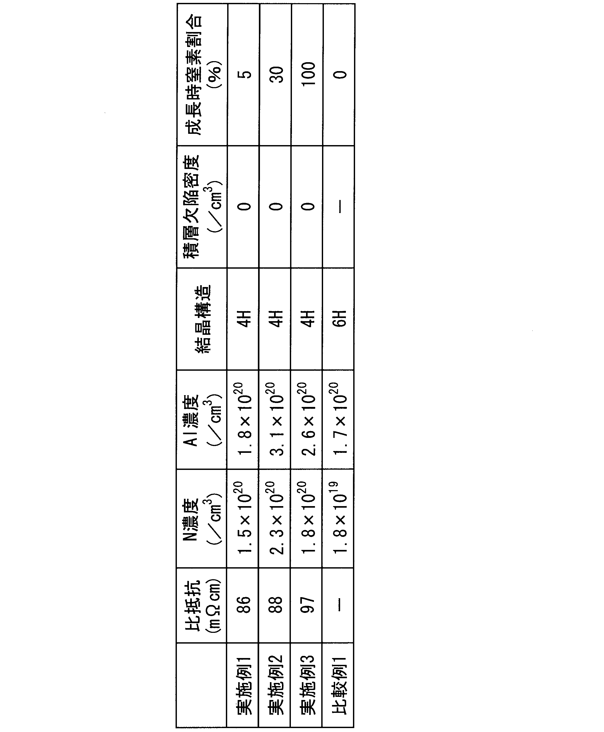
SiC単結晶内に取り込まれている窒素濃度が高いことにより、結晶構造が4HのSiCが安定的に得られている。また実施例1~3のいずれにおいても比抵抗が100mΩcm以下と極めて低く、比抵抗が小さなp型4H-SiC単結晶が得られている。
1…坩堝、2…保持部、3…支持部、4…設置部、5…第1ヒータ、6…第2ヒータ、M1…SiC原料、M2…アルミニウム原料、S…種結晶、R…反応空間
Claims (9)
- アルミニウムと窒素が共にドープされ、
窒素濃度が、2.0×10¹⁹/cm3以上であり、
アルミニウム濃度が1.0×10²⁰/cm3以上であるp型4H-SiC単結晶。 - アルミニウム濃度が1.8×10²⁰/cm3以上である請求項1に記載のp型4H-SiC単結晶。
- 積層欠陥密度が50/cm以下である、請求項1に記載のp型4H-SiC単結晶。
- リン、ヒ素、チタン、バナジウム、クロム、銅、鉄及びニッケルからなる群のいずれの元素の濃度も2×10¹⁵/cm3以下である請求項1に記載のp型4H-SiC単結晶。
- 厚みが1mm以上である請求項1に記載のp型4H-SiC単結晶。
- 窒化されたアルミニウム原料とSiC原料とを昇華させる昇華工程と、
種結晶の一面にアルミニウムと窒素が共ドープされたSiC単結晶を積層する結晶成長工程と、を有するp型4H-SiC単結晶の製造方法。 - 前記昇華工程において、前記窒化されたアルミニウム原料と前記SiC原料とを分離して配置し、それぞれを異なる温度で昇華させる請求項6に記載のp型4H-SiC単結晶の製造方法。
- 前記昇華工程及び前記結晶成長工程を、窒素ガス雰囲気下で行う請求項6に記載のp型4H-SiC単結晶の製造方法。
- 前記昇華工程の前に、アルミニウム原料を窒化し、窒化されたアルミニウム原料を作製する工程を有する請求項6に記載のp型4H-SiC単結晶の製造方法。
Priority Applications (3)
| Application Number | Priority Date | Filing Date | Title |
|---|---|---|---|
| US15/763,596 US20180274125A1 (en) | 2015-09-30 | 2016-09-29 | P-type 4h-sic single crystal and method for producing p-type 4h-sic single crystal |
| CN201680056202.5A CN108026663B (zh) | 2015-09-30 | 2016-09-29 | p型4H-SiC单晶和p型4H-SiC单晶的制造方法 |
| US16/914,506 US11542631B2 (en) | 2015-09-30 | 2020-06-29 | Method for producing p-type 4H-SiC single crystal |
Applications Claiming Priority (2)
| Application Number | Priority Date | Filing Date | Title |
|---|---|---|---|
| JP2015-192724 | 2015-09-30 | ||
| JP2015192724A JP6755524B2 (ja) | 2015-09-30 | 2015-09-30 | p型4H−SiC単結晶及びp型4H−SiC単結晶の製造方法 |
Related Child Applications (2)
| Application Number | Title | Priority Date | Filing Date |
|---|---|---|---|
| US15/763,596 A-371-Of-International US20180274125A1 (en) | 2015-09-30 | 2016-09-29 | P-type 4h-sic single crystal and method for producing p-type 4h-sic single crystal |
| US16/914,506 Division US11542631B2 (en) | 2015-09-30 | 2020-06-29 | Method for producing p-type 4H-SiC single crystal |
Publications (1)
| Publication Number | Publication Date |
|---|---|
| WO2017057581A1 true WO2017057581A1 (ja) | 2017-04-06 |
Family
ID=58423571
Family Applications (1)
| Application Number | Title | Priority Date | Filing Date |
|---|---|---|---|
| PCT/JP2016/078834 Ceased WO2017057581A1 (ja) | 2015-09-30 | 2016-09-29 | p型4H-SiC単結晶及びp型4H-SiC単結晶の製造方法 |
Country Status (4)
| Country | Link |
|---|---|
| US (2) | US20180274125A1 (ja) |
| JP (1) | JP6755524B2 (ja) |
| CN (1) | CN108026663B (ja) |
| WO (1) | WO2017057581A1 (ja) |
Families Citing this family (11)
| Publication number | Priority date | Publication date | Assignee | Title |
|---|---|---|---|---|
| EP3602609B1 (en) * | 2018-02-28 | 2020-04-29 | ABB Power Grids Switzerland AG | Method for p-type doping of silicon carbide by al/be co-implantation |
| JP7068914B2 (ja) | 2018-04-26 | 2022-05-17 | 昭和電工株式会社 | 断熱性遮蔽部材及びそれを備えた単結晶製造装置 |
| JP7170521B2 (ja) | 2018-12-05 | 2022-11-14 | 昭和電工株式会社 | SiC単結晶の評価用サンプル取得方法 |
| CN110129880A (zh) * | 2019-04-26 | 2019-08-16 | 河北同光晶体有限公司 | 一种低碳包裹物密度SiC单晶的生长装置及生长方法 |
| WO2021020574A1 (ja) | 2019-08-01 | 2021-02-04 | ローム株式会社 | 半導体基板及び半導体装置並びにそれらの製造方法 |
| JP7331590B2 (ja) * | 2019-09-27 | 2023-08-23 | 株式会社デンソー | 炭化珪素半導体装置 |
| KR102340110B1 (ko) * | 2019-10-29 | 2021-12-17 | 주식회사 쎄닉 | 탄화규소 잉곳, 웨이퍼 및 이의 제조방법 |
| WO2021149235A1 (ja) * | 2020-01-24 | 2021-07-29 | 日本碍子株式会社 | 希土類含有SiC基板及びSiCエピタキシャル層の製法 |
| DE102020106291B4 (de) * | 2020-03-09 | 2024-02-08 | Ebner Industrieofenbau Gmbh | Heizvorrichtung und Verfahren zur Kristallzüchtung mit beweglicher Impfkristallhalterung |
| CN112522788A (zh) * | 2020-10-30 | 2021-03-19 | 山东天岳先进科技股份有限公司 | 一种富氮碳化硅粉料及其制备方法与应用 |
| JP7845172B2 (ja) * | 2022-12-26 | 2026-04-14 | 株式会社デンソー | 炭化珪素ウェハおよびそれを用いた炭化珪素半導体装置 |
Citations (4)
| Publication number | Priority date | Publication date | Assignee | Title |
|---|---|---|---|---|
| JP2008538542A (ja) * | 2005-04-19 | 2008-10-30 | トゥー‐シックス・インコーポレイテッド | 空間的に均一のドーピング不純物を有するSiC結晶を形成するための方法とそのシステム |
| JP2009167047A (ja) * | 2008-01-15 | 2009-07-30 | Nippon Steel Corp | 炭化珪素単結晶インゴット、これから得られる基板及びエピタキシャルウェハ |
| JP2009179491A (ja) * | 2008-01-29 | 2009-08-13 | Toyota Motor Corp | p型SiC半導体単結晶の製造方法およびそれにより製造されたp型SiC半導体単結晶 |
| JP2014187113A (ja) * | 2013-03-22 | 2014-10-02 | Toshiba Corp | 気相成長装置および気相成長方法 |
Family Cites Families (6)
| Publication number | Priority date | Publication date | Assignee | Title |
|---|---|---|---|---|
| US5433167A (en) * | 1992-02-04 | 1995-07-18 | Sharp Kabushiki Kaisha | Method of producing silicon-carbide single crystals by sublimation recrystallization process using a seed crystal |
| US6063185A (en) | 1998-10-09 | 2000-05-16 | Cree, Inc. | Production of bulk single crystals of aluminum nitride, silicon carbide and aluminum nitride: silicon carbide alloy |
| US7316747B2 (en) * | 2002-06-24 | 2008-01-08 | Cree, Inc. | Seeded single crystal silicon carbide growth and resulting crystals |
| US7422634B2 (en) * | 2005-04-07 | 2008-09-09 | Cree, Inc. | Three inch silicon carbide wafer with low warp, bow, and TTV |
| JP5839315B2 (ja) * | 2010-07-30 | 2016-01-06 | 株式会社デンソー | 炭化珪素単結晶およびその製造方法 |
| JP6152981B2 (ja) | 2013-08-02 | 2017-06-28 | 株式会社デンソー | 炭化珪素単結晶 |
-
2015
- 2015-09-30 JP JP2015192724A patent/JP6755524B2/ja active Active
-
2016
- 2016-09-29 US US15/763,596 patent/US20180274125A1/en not_active Abandoned
- 2016-09-29 WO PCT/JP2016/078834 patent/WO2017057581A1/ja not_active Ceased
- 2016-09-29 CN CN201680056202.5A patent/CN108026663B/zh active Active
-
2020
- 2020-06-29 US US16/914,506 patent/US11542631B2/en active Active
Patent Citations (4)
| Publication number | Priority date | Publication date | Assignee | Title |
|---|---|---|---|---|
| JP2008538542A (ja) * | 2005-04-19 | 2008-10-30 | トゥー‐シックス・インコーポレイテッド | 空間的に均一のドーピング不純物を有するSiC結晶を形成するための方法とそのシステム |
| JP2009167047A (ja) * | 2008-01-15 | 2009-07-30 | Nippon Steel Corp | 炭化珪素単結晶インゴット、これから得られる基板及びエピタキシャルウェハ |
| JP2009179491A (ja) * | 2008-01-29 | 2009-08-13 | Toyota Motor Corp | p型SiC半導体単結晶の製造方法およびそれにより製造されたp型SiC半導体単結晶 |
| JP2014187113A (ja) * | 2013-03-22 | 2014-10-02 | Toshiba Corp | 気相成長装置および気相成長方法 |
Non-Patent Citations (1)
| Title |
|---|
| A. KAKANAKOVA-GEORGIEVA ET AL.: "Site-occupying behavior of boron in compensated p-type 4H-SiC grown by sublimation epitaxy", JOURNAL OF APPLIED PHYSICS, vol. 91, no. 5, pages 3471 - 3473, XP012055976 * |
Also Published As
| Publication number | Publication date |
|---|---|
| JP6755524B2 (ja) | 2020-09-16 |
| JP2017065959A (ja) | 2017-04-06 |
| CN108026663B (zh) | 2021-05-11 |
| US11542631B2 (en) | 2023-01-03 |
| CN108026663A (zh) | 2018-05-11 |
| US20180274125A1 (en) | 2018-09-27 |
| US20200325595A1 (en) | 2020-10-15 |
Similar Documents
| Publication | Publication Date | Title |
|---|---|---|
| US11542631B2 (en) | Method for producing p-type 4H-SiC single crystal | |
| CN101194052B (zh) | 低基面位错块体生长的SiC晶片 | |
| JP5562641B2 (ja) | マイクロパイプ・フリーの炭化ケイ素およびその製造方法 | |
| US7314521B2 (en) | Low micropipe 100 mm silicon carbide wafer | |
| US7314520B2 (en) | Low 1c screw dislocation 3 inch silicon carbide wafer | |
| US10892334B2 (en) | n-Type SiC single crystal substrate, method for producing same and SiC epitaxial wafer | |
| JP5865777B2 (ja) | 炭化珪素エピタキシャルウェハの製造方法 | |
| KR100773624B1 (ko) | 탄화 규소 단결정으로 이루어지는 종결정 및 그를 이용한잉곳의 제조 방법 | |
| KR20110071092A (ko) | 탄화규소 단결정 및 탄화규소 단결정 웨이퍼 | |
| JP6624868B2 (ja) | p型低抵抗率炭化珪素単結晶基板 | |
| WO2015170500A1 (ja) | SiCエピタキシャルウエハおよび炭化珪素半導体装置の製造方法 | |
| JP5943509B2 (ja) | 炭化珪素基板への成膜方法 | |
| TW202126866A (zh) | 碳化矽基板、碳化矽基板的製造方法、碳化矽半導體裝置以及碳化矽半導體裝置的製造方法 | |
| JP5131262B2 (ja) | 炭化珪素単結晶及びその製造方法 | |
| JP5115413B2 (ja) | 炭化珪素単結晶の製造装置および製造方法 | |
| JP2018168052A (ja) | 炭化珪素単結晶インゴットの製造方法 | |
| WO2023054264A1 (ja) | 炭化ケイ素単結晶ウエハ及び炭化ケイ素単結晶インゴット |
Legal Events
| Date | Code | Title | Description |
|---|---|---|---|
| 121 | Ep: the epo has been informed by wipo that ep was designated in this application |
Ref document number: 16851752 Country of ref document: EP Kind code of ref document: A1 |
|
| WWE | Wipo information: entry into national phase |
Ref document number: 15763596 Country of ref document: US |
|
| NENP | Non-entry into the national phase |
Ref country code: DE |
|
| 122 | Ep: pct application non-entry in european phase |
Ref document number: 16851752 Country of ref document: EP Kind code of ref document: A1 |