WO2017056744A1 - レーザ加工方法及びレーザ加工装置 - Google Patents
レーザ加工方法及びレーザ加工装置 Download PDFInfo
- Publication number
- WO2017056744A1 WO2017056744A1 PCT/JP2016/073468 JP2016073468W WO2017056744A1 WO 2017056744 A1 WO2017056744 A1 WO 2017056744A1 JP 2016073468 W JP2016073468 W JP 2016073468W WO 2017056744 A1 WO2017056744 A1 WO 2017056744A1
- Authority
- WO
- WIPO (PCT)
- Prior art keywords
- cutting line
- modified region
- silicon substrate
- planned cutting
- distance
- Prior art date
- Legal status (The legal status is an assumption and is not a legal conclusion. Google has not performed a legal analysis and makes no representation as to the accuracy of the status listed.)
- Ceased
Links
Images













Classifications
-
- B—PERFORMING OPERATIONS; TRANSPORTING
- B23—MACHINE TOOLS; METAL-WORKING NOT OTHERWISE PROVIDED FOR
- B23K—SOLDERING OR UNSOLDERING; WELDING; CLADDING OR PLATING BY SOLDERING OR WELDING; CUTTING BY APPLYING HEAT LOCALLY, e.g. FLAME CUTTING; WORKING BY LASER BEAM
- B23K26/00—Working by laser beam, e.g. welding, cutting or boring
- B23K26/50—Working by transmitting the laser beam through or within the workpiece
- B23K26/53—Working by transmitting the laser beam through or within the workpiece for modifying or reforming the material inside the workpiece, e.g. for producing break initiation cracks
-
- B—PERFORMING OPERATIONS; TRANSPORTING
- B23—MACHINE TOOLS; METAL-WORKING NOT OTHERWISE PROVIDED FOR
- B23K—SOLDERING OR UNSOLDERING; WELDING; CLADDING OR PLATING BY SOLDERING OR WELDING; CUTTING BY APPLYING HEAT LOCALLY, e.g. FLAME CUTTING; WORKING BY LASER BEAM
- B23K26/00—Working by laser beam, e.g. welding, cutting or boring
- B23K26/0006—Working by laser beam, e.g. welding, cutting or boring taking account of the properties of the material involved
-
- B—PERFORMING OPERATIONS; TRANSPORTING
- B23—MACHINE TOOLS; METAL-WORKING NOT OTHERWISE PROVIDED FOR
- B23K—SOLDERING OR UNSOLDERING; WELDING; CLADDING OR PLATING BY SOLDERING OR WELDING; CUTTING BY APPLYING HEAT LOCALLY, e.g. FLAME CUTTING; WORKING BY LASER BEAM
- B23K26/00—Working by laser beam, e.g. welding, cutting or boring
- B23K26/02—Positioning or observing the workpiece, e.g. with respect to the point of impact; Aligning, aiming or focusing the laser beam
- B23K26/04—Automatically aligning, aiming or focusing the laser beam, e.g. using the back-scattered light
-
- B—PERFORMING OPERATIONS; TRANSPORTING
- B23—MACHINE TOOLS; METAL-WORKING NOT OTHERWISE PROVIDED FOR
- B23K—SOLDERING OR UNSOLDERING; WELDING; CLADDING OR PLATING BY SOLDERING OR WELDING; CUTTING BY APPLYING HEAT LOCALLY, e.g. FLAME CUTTING; WORKING BY LASER BEAM
- B23K26/00—Working by laser beam, e.g. welding, cutting or boring
- B23K26/02—Positioning or observing the workpiece, e.g. with respect to the point of impact; Aligning, aiming or focusing the laser beam
- B23K26/04—Automatically aligning, aiming or focusing the laser beam, e.g. using the back-scattered light
- B23K26/046—Automatically focusing the laser beam
- B23K26/048—Automatically focusing the laser beam by controlling the distance between laser head and workpiece
-
- B—PERFORMING OPERATIONS; TRANSPORTING
- B23—MACHINE TOOLS; METAL-WORKING NOT OTHERWISE PROVIDED FOR
- B23K—SOLDERING OR UNSOLDERING; WELDING; CLADDING OR PLATING BY SOLDERING OR WELDING; CUTTING BY APPLYING HEAT LOCALLY, e.g. FLAME CUTTING; WORKING BY LASER BEAM
- B23K26/00—Working by laser beam, e.g. welding, cutting or boring
- B23K26/02—Positioning or observing the workpiece, e.g. with respect to the point of impact; Aligning, aiming or focusing the laser beam
- B23K26/06—Shaping the laser beam, e.g. by masks or multi-focusing
- B23K26/062—Shaping the laser beam, e.g. by masks or multi-focusing by direct control of the laser beam
- B23K26/0622—Shaping the laser beam, e.g. by masks or multi-focusing by direct control of the laser beam by shaping pulses
-
- B—PERFORMING OPERATIONS; TRANSPORTING
- B23—MACHINE TOOLS; METAL-WORKING NOT OTHERWISE PROVIDED FOR
- B23K—SOLDERING OR UNSOLDERING; WELDING; CLADDING OR PLATING BY SOLDERING OR WELDING; CUTTING BY APPLYING HEAT LOCALLY, e.g. FLAME CUTTING; WORKING BY LASER BEAM
- B23K26/00—Working by laser beam, e.g. welding, cutting or boring
- B23K26/08—Devices involving relative movement between laser beam and workpiece
-
- B—PERFORMING OPERATIONS; TRANSPORTING
- B23—MACHINE TOOLS; METAL-WORKING NOT OTHERWISE PROVIDED FOR
- B23K—SOLDERING OR UNSOLDERING; WELDING; CLADDING OR PLATING BY SOLDERING OR WELDING; CUTTING BY APPLYING HEAT LOCALLY, e.g. FLAME CUTTING; WORKING BY LASER BEAM
- B23K26/00—Working by laser beam, e.g. welding, cutting or boring
- B23K26/36—Removing material
- B23K26/38—Removing material by boring or cutting
-
- H—ELECTRICITY
- H10—SEMICONDUCTOR DEVICES; ELECTRIC SOLID-STATE DEVICES NOT OTHERWISE PROVIDED FOR
- H10P—GENERIC PROCESSES OR APPARATUS FOR THE MANUFACTURE OR TREATMENT OF DEVICES COVERED BY CLASS H10
- H10P54/00—Cutting or separating of wafers, substrates or parts of devices
-
- B—PERFORMING OPERATIONS; TRANSPORTING
- B23—MACHINE TOOLS; METAL-WORKING NOT OTHERWISE PROVIDED FOR
- B23K—SOLDERING OR UNSOLDERING; WELDING; CLADDING OR PLATING BY SOLDERING OR WELDING; CUTTING BY APPLYING HEAT LOCALLY, e.g. FLAME CUTTING; WORKING BY LASER BEAM
- B23K2103/00—Materials to be soldered, welded or cut
- B23K2103/50—Inorganic materials other than metals or composite materials
- B23K2103/56—Inorganic materials other than metals or composite materials being semiconducting
Definitions
- One aspect of the present invention relates to a laser processing method and a laser processing apparatus.
- a processing object including a silicon substrate having a plurality of functional elements formed in a matrix on the surface with a laser beam on the back surface of the silicon substrate as a laser beam incident surface
- the workpiece passes between adjacent functional elements.
- a modified region near the surface of the silicon substrate along the planned cutting line set in a lattice shape and then polishing the back surface of the silicon substrate so that the silicon substrate has a predetermined thickness.
- a laser processing method for cutting an object for each functional element is known (see, for example, Patent Document 1).
- the laser processing method as described above it is possible to reduce the number of scans of the laser beam with respect to one scheduled cutting line (that is, the number of columns in which the modified region is formed with respect to one scheduled cutting line). Is important. Therefore, there is a case where a crack is greatly extended from the modified region in the thickness direction of the silicon substrate with the formation of the modified region by condensing laser light having a high transmittance with respect to silicon on the silicon substrate.
- laser light having a high transmittance with respect to silicon is condensed on the silicon substrate, the surface of the silicon substrate opposite to the laser light incident surface may be damaged, and the characteristics of the functional element may be deteriorated.
- a processing object there is a thing including the above-mentioned silicon substrate, an effective region including a functional element formed on the silicon substrate, and an ineffective region formed on the silicon substrate.
- the effective area is an area that becomes a chip including a functional element by cutting the processing object
- the ineffective area is an area that becomes unnecessary by cutting the processing object.
- An object of one aspect of the present invention is to provide a laser processing method and a laser processing apparatus capable of suppressing deterioration of characteristics of functional elements.
- a laser processing method includes a semiconductor substrate having a front surface and a back surface, a plurality of effective regions formed on the surface, and an ineffective region formed on the surface between the effective regions.
- the laser beam is condensed on the workpiece to be processed with the back surface as the incident surface, and the distance between the front surface and the first focal point of the laser beam is maintained at the first distance, and the effective area and the ineffective area adjacent to each other are maintained.
- the first step of forming the first modified region along the planned cutting line by moving the first condensing point along the planned cutting line set to pass between Concentrate laser light on the workpiece with the back surface as the incident surface, and maintain the distance between the front surface and the second condensing point of the laser light at a second distance larger than the first distance
- the second condensing point Along the planned cutting line by moving the second condensing point along A second step of forming a modified region, wherein the effective region includes a functional element, and in the second step, a direction perpendicular to both the thickness direction of the semiconductor substrate and the extending direction of the line to be cut
- the second focusing point is moved along the scheduled cutting line while offsetting the second focusing point to the effective region side from the position where the first focusing point is combined.
- the laser in the second step, is perpendicular to both the thickness direction of the semiconductor substrate and the extending direction of the line to be cut with respect to the position where the first condensing point of the laser beam is aligned.
- the second light condensing point is offset.
- the second condensing point is offset to the effective region side from the position where the first condensing point is combined.
- the position where damage may occur with respect to the surface of the workpiece can be shifted to the ineffective region side. That is, the position where damage can occur can be controlled to the non-effective region side rather than the effective region including the functional element. From the above viewpoint, according to this laser processing method, it is possible to suppress the deterioration of the characteristics of the functional element.
- the semiconductor substrate may be a silicon substrate, and the laser beam may have a wavelength greater than 1064 nm.
- the thickness of the semiconductor substrate from the first modified region and the second modified region is increased with the formation of the first modified region and the second modified region.
- the crack can be greatly extended in the direction. Therefore, processing efficiency can be improved.
- the laser beam may have a wavelength of 1099 ⁇ m to 1342 ⁇ m.
- the cracks can be further extended from the first modified region and the second modified region in the thickness direction of the semiconductor substrate with the formation of the first modified region and the second modified region.
- the second focusing is performed in a direction perpendicular to both the thickness direction of the semiconductor substrate and the extending direction of the line to be cut with respect to the position where the first focusing points are aligned.
- the distance for offsetting the light spot may be 24 ⁇ m or less.
- a crack is reliably connected between the first modified region and the second modified region, and the first modified region and the second modified region are formed along with the formation of the first modified region and the second modified region.
- a crack can be reliably extended from the quality region to the thickness direction of the semiconductor substrate.
- the second focusing is performed in a direction perpendicular to both the thickness direction of the semiconductor substrate and the extending direction of the line to be cut with respect to the position where the first focusing points are aligned.
- the distance for offsetting the light spot may be not less than 2 ⁇ m and not more than 8 ⁇ m. In this case, the distance of the offset of the second condensing point can be in a necessary and sufficient range.
- the first focusing is performed in a direction perpendicular to both the thickness direction of the semiconductor substrate and the extending direction of the planned cutting line with respect to the planned cutting line. You may move a 1st condensing point along a cutting plan line, maintaining the distance which offsets a point to 0. In this case, a crack extending from the first modified region to the surface side of the semiconductor substrate can be matched with the planned cutting line.
- a laser processing apparatus includes a semiconductor substrate having a front surface and a back surface, a plurality of effective regions formed on the surface, and an ineffective region formed on the surface between the effective regions.
- the laser beam emitted from the laser light source is focused on the workpiece that is supported by the support base that supports the workpiece, the laser light source that emits laser light, and the workpiece that is supported by the support base so that the back surface is the incident surface.
- the first condensing point is moved along the scheduled cutting line set so as to pass between the adjacent effective region and the non-effective region while maintaining the distance from the one condensing point to the first distance
- the distance between the surface and the second focal point of the laser beam is While maintaining the second distance larger than the distance, and on the effective region side from the position where the first light focusing points are aligned in the direction perpendicular to both the thickness direction of the semiconductor substrate and the extending direction of the line to be cut.
- the second condensing point is moved along the scheduled cutting line while offsetting the second condensing point.
- the laser processing apparatus for the same reason as the laser processing method described above, it is possible to suppress the occurrence of damage on the surface of the object to be processed on the side opposite to the laser light incident surface, and at the position where the damage can occur,
- the effective area including the functional element can be controlled to the non-effective area side. Therefore, it is possible to suppress the deterioration of the characteristics of the functional element.
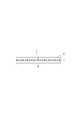
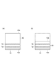
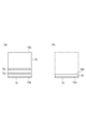
- FIG. 3 is a cross-sectional view taken along the line III-III of the workpiece in FIG. 2. It is a top view of the processing target after laser processing.
- FIG. 5 is a cross-sectional view taken along the line VV of the workpiece in FIG. 4.
- FIG. 5 is a cross-sectional view taken along line VI-VI of the workpiece in FIG. 4.
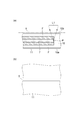
- A) is sectional drawing along the cutting scheduled line of the process target object in laser processing.
- (B) is a top view of the processed object after a cutting
- (A) is sectional drawing along the cutting scheduled line of the process target object in laser processing.
- (B) is a top view of the processed object after a cutting
- (A) is sectional drawing along the cutting scheduled line of the process target object in laser processing.
- (B) is a top view of the processed object after a cutting
- (A) is sectional drawing along the cutting scheduled line of the process target object in laser processing.
- (B) is a top view of the processed object after a cutting
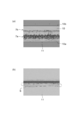
- (A) is a figure which shows the photograph of the surface parallel to the cutting scheduled line of the silicon substrate after a cutting
- (B) is a figure which shows the photograph of the surface side of the silicon substrate after a cutting
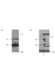
- (A) is a figure which shows the photograph of the surface parallel to the cutting plan line of the silicon substrate after 1st modified region and 2nd modified region formation.
- (B) is a figure which shows the photograph of a surface perpendicular
- (A) is a figure which shows the photograph of the surface parallel to the cutting plan line of the silicon substrate after 1st modified region and 2nd modified region formation.
- (B) is a figure which shows the photograph of a surface perpendicular
- (A) is a figure which shows the photograph of the surface parallel to the cutting scheduled line of the silicon substrate after a cutting
- (B) is a figure which shows the photograph of the surface side of the silicon substrate after a cutting
- A) is a figure which shows the photograph of the surface side of the silicon substrate after a cutting
- B) is a figure which shows the photograph of the surface side of the silicon substrate after a cutting
- (C) is a figure which shows the photograph of the surface side of the silicon substrate after a cutting
- (A) is a figure which shows a surface perpendicular
- (B) is a figure which shows a surface perpendicular
- the modified region is formed in the processing object along the planned cutting line by condensing the laser beam on the processing object.
- the formation of the modified region will be described with reference to FIGS.
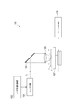
- a laser processing apparatus 100 includes a laser light source 101 that oscillates a laser beam L, a dichroic mirror 103 that is arranged to change the direction of the optical axis (optical path) of the laser beam L by 90 °, and And a condensing lens 105 for condensing the laser light L. Further, the laser processing apparatus 100 includes a support base 107 for supporting the workpiece 1 irradiated with the laser light L condensed by the condensing lens 105, and a stage 111 for moving the support base 107. , A laser light source control unit 102 for controlling the laser light source 101 to adjust the output, pulse width, pulse waveform, and the like of the laser light L, and a stage control unit 115 for controlling the movement of the stage 111.
- the laser light L emitted from the laser light source 101 is changed in the direction of its optical axis by 90 ° by the dichroic mirror 103, and is placed inside the processing object 1 placed on the support base 107.
- the light is condensed by the condensing lens 105.
- the stage 111 is moved, and the workpiece 1 is moved relative to the laser beam L along the planned cutting line 5. Thereby, a modified region along the planned cutting line 5 is formed on the workpiece 1.
- the stage 111 is moved in order to move the laser light L relatively, but the condensing lens 105 may be moved, or both of them may be moved.
- a plate-like member for example, a substrate, a wafer, or the like
- a scheduled cutting line 5 for cutting the workpiece 1 is set in the workpiece 1.
- the planned cutting line 5 is a virtual line extending linearly.
- the laser beam L is cut in a state where the condensing point (condensing position) P is aligned with the inside of the workpiece 1 as shown in FIG. 3. It moves relatively along the planned line 5 (that is, in the direction of arrow A in FIG. 2).
- the modified region 7 is formed on the workpiece 1 along the planned cutting line 5, and the modified region formed along the planned cutting line 5. 7 becomes the cutting start region 8.
- the condensing point P is a portion where the laser light L is condensed.
- the planned cutting line 5 is not limited to a straight line, but may be a curved line, a three-dimensional shape in which these lines are combined, or a coordinate designated.
- the planned cutting line 5 is not limited to a virtual line but may be a line actually drawn on the surface 3 of the workpiece 1.
- the modified region 7 may be formed continuously or intermittently.
- the modified region 7 may be in the form of a line or a dot. In short, the modified region 7 only needs to be formed at least inside the workpiece 1.
- a crack may be formed starting from the modified region 7, and the crack and the modified region 7 may be exposed on the outer surface (front surface 3, back surface, or outer peripheral surface) of the workpiece 1. .
- the laser light incident surface when forming the modified region 7 is not limited to the front surface 3 of the workpiece 1 and may be the back surface of the workpiece 1.
- the modified region 7 when the modified region 7 is formed inside the workpiece 1, the laser light L passes through the workpiece 1 and is near the condensing point P located inside the workpiece 1. Especially absorbed. Thereby, the modified region 7 is formed in the workpiece 1 (that is, internal absorption laser processing). In this case, since the laser beam L is hardly absorbed by the surface 3 of the workpiece 1, the surface 3 of the workpiece 1 is not melted. On the other hand, when the modified region 7 is formed on the surface 3 of the workpiece 1, the laser light L is absorbed particularly near the condensing point P located on the surface 3 and melted and removed from the surface 3. Then, removal portions such as holes and grooves are formed (surface absorption laser processing).
- the modified region 7 is a region where the density, refractive index, mechanical strength and other physical characteristics are different from the surroundings.
- Examples of the modified region 7 include a melt treatment region (meaning at least one of a region once solidified after melting, a region in a molten state, and a region in a state of being resolidified from melting), a crack region, and the like.
- a dielectric breakdown region, a refractive index change region, etc. there is a region where these are mixed.
- the modified region 7 includes a region where the density of the modified region 7 in the material of the workpiece 1 is changed compared to the density of the non-modified region, and a region where lattice defects are formed.
- the modified region 7 can be said to be a high dislocation density region.
- the area where the density of the melt processing area, the refractive index changing area, the density of the modified area 7 is changed as compared with the density of the non-modified area, and the area where lattice defects are formed are further included in the interior of these areas or the modified areas.
- cracks (cracks, microcracks) are included in the interface between the region 7 and the non-modified region.
- the included crack may be formed over the entire surface of the modified region 7, or may be formed in only a part or a plurality of parts.
- the workpiece 1 includes a substrate made of a crystal material having a crystal structure.
- the workpiece 1 includes a substrate formed of at least one of gallium nitride (GaN), silicon (Si), silicon carbide (SiC), LiTaO 3 , and sapphire (Al 2 O 3 ).
- the workpiece 1 includes, for example, a gallium nitride substrate, a silicon substrate, a SiC substrate, a LiTaO 3 substrate, or a sapphire substrate.
- the crystal material may be either an anisotropic crystal or an isotropic crystal.
- the workpiece 1 may include a substrate made of an amorphous material having an amorphous structure (amorphous structure), for example, a glass substrate.
- the modified region 7 can be formed by forming a plurality of modified spots (processing marks) along the planned cutting line 5.
- the modified region 7 is formed by collecting a plurality of modified spots.
- the modified spot is a modified portion formed by one pulse shot of pulsed laser light (that is, one pulse of laser irradiation: laser shot).
- Examples of the modified spot include a crack spot, a melting treatment spot, a refractive index change spot, or a mixture of at least one of these.
- the size and length of cracks to be generated are appropriately determined in consideration of the required cutting accuracy, required flatness of the cut surface, thickness, type, crystal orientation, etc. of the workpiece 1. Can be controlled.
- the modified spot can be formed as the modified region 7 along the planned cutting line 5.
- a metal substrate 11 formed on the surface 10a of the silicon substrate 10 was prepared as an object to be processed.
- the metal film 11 is constituted by forming a 20 ⁇ m thick Cr film on the surface 10 a of the silicon substrate 10 and forming a 50 ⁇ m thick Au film on the Cr film.
- the back surface 10b of the silicon substrate 10 is used as the laser light incident surface, and the laser light L0 having a wavelength of 1064 nm is condensed inside the silicon substrate 10 to form the line 5 to be cut.
- the modified region 7 was formed inside the silicon substrate 10 along the planned cutting line 5 by moving the condensing point P of the laser beam L0 along the line.
- the crack F that extends in the thickness direction of the silicon substrate 10 from the modified region 7 with the formation of the modified region 7 (that is, the formation of the modified region 7 without applying an external force to the silicon substrate 10).
- the irradiation conditions of the laser beam L0 were adjusted so that the cracks F) generated along with the laser beam L0 reached the surface 10a of the silicon substrate 10. In this case, as shown in FIG. 7B, the metal film 11 was not splashed.
- the back surface 10b of the silicon substrate 10 is used as the laser light incident surface, and the laser light L1 having a wavelength of 1342 nm is condensed inside the silicon substrate 10 to form the cutting line 5
- the modified region 7 was formed inside the silicon substrate 10 along the planned cutting line 5 by moving the condensing point P of the laser beam L1 along the line.
- the irradiation condition of the laser beam L1 was adjusted so that the crack F extending from the modified region 7 reached the surface 10a of the silicon substrate 10.
- the irradiation conditions of the laser beam L1 are the same as the irradiation conditions of the laser beam L0 described above, except that the wavelengths are different.
- a splash S was generated in the metal film 11.
- the back surface 10b of the silicon substrate 10 is used as the laser light incident surface, and the laser light L1 having a wavelength of 1342 nm is condensed inside the silicon substrate 10 to form the line 5 to be cut.
- the modified region 7 was formed inside the silicon substrate 10 along the planned cutting line 5 by moving the condensing point P of the laser beam L1 along the line.
- the irradiation condition of the laser beam L1 was adjusted so that the crack F extending from the modified region 7 did not reach the surface 10a of the silicon substrate 10 and was contained in the silicon substrate 10.
- the pulse energy of the laser beam L1 is made smaller than in the case of FIG. In this case, as shown in FIG. 9B, the metal film 11 was not splashed.
- the back surface 10b of the silicon substrate 10 is used as the laser light incident surface, and the laser light L1 having a wavelength of 1342 nm is condensed inside the silicon substrate 10 to form the cutting line 5
- the first modified region 7a and the second modified region 7b were formed inside the silicon substrate 10 along the planned cutting line 5 by moving the condensing point P of the laser beam L1 along the line.
- the crack F does not reach the front surface 10a of the silicon substrate 10 only by forming the first modified region 7a, and the second modified region on the back surface 10b side of the silicon substrate 10 with respect to the first modified region 7a.
- the irradiation condition of the laser beam L1 was adjusted so that the crack F reached the surface 10a of the silicon substrate 10 when 7b was formed. In this case, as shown in FIG. 10B, a splash S was generated in the metal film 11.
- FIG. 11 is a view showing a photograph of the silicon substrate 10 when the first modified region 7a and the second modified region 7b are formed in the silicon substrate 10 under the conditions of FIG. More specifically, FIG. 11A is a diagram showing a photograph of a plane parallel to the planned cutting line of the silicon substrate 10 after cutting, and FIG. 11B is a diagram showing the silicon substrate 10 after cutting. It is a figure which shows the photograph of the surface 10a side (metal film 11). Referring to (b) of FIG. 11, it can be confirmed that a dark portion exists in the region surrounded by the alternate long and short dash line in the metal film 11. This is the splash S that becomes a problem.
- the crack F is larger from the modified region 7 in the thickness direction of the silicon substrate 10 than when the laser beam L0 having a wavelength of 1064 nm or less is used. Can be extended. Further, when the laser light L1 having a wavelength larger than 1064 nm, such as 1342 nm, is used, the modified region is deeper than the laser light incident surface of the silicon substrate 10 as compared with the case where the laser light L0 having a wavelength of 1064 nm or less is used. 7 can be formed.
- the laser beam L1 having a wavelength larger than 1064 nm has a higher transmittance with respect to silicon than the laser beam L0 having a wavelength of 1064 nm or less. Therefore, from the viewpoint of improving the processing efficiency by reducing the number of scans of the laser light L for one scheduled cutting line 5 (that is, the number of columns in which the modified region 7 is formed for one scheduled cutting line 5), It is desirable to use laser light L1 having a wavelength larger than 1064 nm.
- the splash S is formed on the metal film 11.
- a functional element for example, a semiconductor operating layer formed by crystal growth, a light receiving element such as a photodiode, a light emitting element such as a laser diode, or a circuit is formed on the surface 10a of the silicon substrate 10 opposite to the laser light incident surface. If a splash S occurs when a circuit element or the like is formed, the characteristics of the functional element may be deteriorated.
- the splash S is generated on the surface 10a of the silicon substrate 10 when the laser light L1 having a wavelength larger than 1064 nm is used, and the laser light is applied to the crack F greatly extended from the formed modified region 7.
- L1 is condensed, which is considered to be caused by an increase in the influence of missing light (light that escapes to the surface 10a side of the silicon substrate 10 without contributing to the formation of the modified region 7 in the laser light L1).
- the present inventors when forming the second modified region 7b in the case of FIG. 10, if the condensing point P of the laser beam L1 is offset, the omission that causes the occurrence of the splash S. The following verification was performed on the assumption that the influence of light could be reduced.
- the thickness direction of the silicon substrate 10 and the position where the condensing point P of the laser beam L1 is aligned when the first modified region 7a is formed "Laser focusing point P of laser beam L1 is offset in a direction perpendicular to both of the extending directions of cutting line 5 (the direction perpendicular to the cross section of silicon substrate 10 in FIG. 10A)” It is referred to as “offset the condensing point P of the light L1”, and “distance to offset the condensing point P of the laser light L1” is referred to as “offset amount”.
- FIG. 12 is a view showing a photograph of the silicon substrate 10 when the condensing point P of the laser beam L1 is not offset when forming the second modified region 7b. More specifically, FIG. 12A is a diagram showing a photograph of a plane parallel to the planned cutting line of the silicon substrate 10 after the formation of the first modified region 7a and the second modified region 7b. 12B is a diagram showing a photograph of a surface perpendicular to the planned cutting line of the silicon substrate 10 after the formation of the first modified region 7a and the second modified region 7b. Referring to (b) of FIG.
- FIG. 13 is a view showing a photograph of the silicon substrate 10 when the condensing point P of the laser beam L1 is offset when the second modified region 7b is formed (when the offset amount is 8 ⁇ m). More specifically, FIG. 13A is a diagram showing a photograph of a plane parallel to the planned cutting line of the silicon substrate 10 after the formation of the first modified region 7a and the second modified region 7b. 13B is a view showing a photograph of a surface perpendicular to the planned cutting line of the silicon substrate 10 after the formation of the first modified region 7a and the second modified region 7b. Referring to FIG.
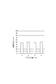
- FIG. 14 is a graph showing the relationship between the offset amount and the length of the crack F.
- the length of the crack F is the length of the crack F extending from the first modified region 7a to the surface 10a side of the silicon substrate 10.
- the condensing point P of the laser beam L1 may be offset or not offset (even when the offset amount is 0 ⁇ m). It can be confirmed that the length of the crack F extending from 7a to the surface 10a side of the silicon substrate 10 does not change.
- FIG. 15 is a graph showing the relationship between the offset amount and the number of splashes S.
- the number of splashes S is the number of splashes S (the number per 15 mm in length of the planned cutting line 5) generated in a region separated by 20 ⁇ m or more on both sides from the planned cutting line 5.
- the condensing point P of the laser beam L1 is offset when forming the second modified region 7b, the number of splashes S is reduced as compared with the case where the offset is not offset (when the offset amount is 0 ⁇ m). I can confirm that.
- the number of the splashes S generated in the regions separated by 20 ⁇ m or more on both sides from the scheduled cutting line 5 is counted particularly because the characteristics of the functional elements formed on the surface 10 a of the silicon substrate 10 are such splashes S. This is because it causes a problem of deterioration. Dicing streets (regions between adjacent functional elements) are often provided in regions within 20 ⁇ m on both sides of the planned cutting line 5, so that the splash S generated in the region causes a problem of deteriorating the characteristics of the functional devices. Unlikely.
- FIG. 16 is a view showing a photograph of the silicon substrate 10 when the condensing point P of the laser beam L1 is offset when forming the second modified region 7b. More specifically, FIG. 16A is a diagram showing a photograph of a surface parallel to the cutting line 5 of the silicon substrate 10 after cutting, and FIG. 16B is a silicon substrate after cutting. 10 is a view showing a photograph of the surface 10a side (metal film 11) of FIG. Referring to FIG. 16A, the first modified region 7a and the second modified region that have already been formed by offsetting the condensing point P of the laser beam L1 when forming the second modified region 7b.
- the laser beam L1 is suppressed from being focused on the crack F extending from the region 7b, and the second modified region 7b is formed to be large. That is, it is considered that the ratio of the laser beam L1 that contributes to the formation of the second modified region 7b increases and the ratio of the missing light decreases. Referring to FIG. 16B, it can be confirmed that the splash S is not generated.
- FIG. 11 (a) showing a photograph of the silicon substrate 10 when the condensing point P of the laser beam L1 is not offset when forming the second modified region 7b
- the second modification is made. It can be confirmed that the mass region 7b is formed small. This is considered to be due to the fact that the laser beam L1 is condensed on the crack F extending from the first modified region 7a and the second modified region 7b that have been formed, and the amount of light passing through is increased.
- the laser light irradiation conditions other than the offset amount are the same.
- FIG. 17 is a view showing a photograph of the surface 10a side (metal film 11) of the silicon substrate 10 after cutting. More specifically, FIG. 17A shows the case where the offset amount is 2 ⁇ m, FIG. 17B shows the case where the offset amount is 4 ⁇ m, and FIG. 17C shows the case where the offset amount is 6 ⁇ m. Is the case. In each case, the irradiation conditions of the laser light other than the offset amount are the same. Referring to FIGS. 17A and 17B, when forming the second modified region 7b, the splash S is generated on the side opposite to the side where the condensing point P of the laser beam L1 is offset. It can be confirmed that the splash S is further away from the planned cutting line 5 as the offset amount is increased.
- FIGS. 17A, 17B, and 17C it can be confirmed that the region where the splash S is generated decreases as the offset amount increases. Even in the cases of FIGS. 17A and 17B, the region where the splash S is generated compared to the case where the condensing point P of the laser beam L1 is not offset when forming the second modified region 7b. Is decreasing.
- FIG. 18A is a diagram showing a surface perpendicular to the cutting line 5 of the silicon substrate 10 when the offset amount is small
- FIG. 18B is a diagram of the silicon substrate 10 when the offset amount is large. It is a figure which shows a surface perpendicular
- the second laser beam L1 of the crack F extending from the first modified region 7a and the second modified region 7b that has been formed.
- a portion F1 to which the condensing point P2 is matched is inclined at a small angle with respect to the thickness direction D of the silicon substrate 10. Therefore, the incident angle ⁇ of the laser beam L1 with respect to the portion F1 increases. Therefore, the light L2 that has not contributed to the formation of the second modified region 7b in the laser light L1 offsets the condensing point P of the laser light L1 at a small angle with respect to the thickness direction D of the silicon substrate 10. Proceeds to the opposite side to the side that has been made.
- the optical path length of the escape light L2 reaching the surface 10a of the silicon substrate 10 is shortened, and the amount of absorption and the degree of scattering of the escape light L2 in the silicon substrate 10 are reduced. Note that “small”, “large”, “short”, and the like are used in comparison with the case of FIG.
- a workpiece 1 is prepared.
- the workpiece 1 includes a silicon substrate (semiconductor substrate) 10 and a functional element layer 15.
- Silicon substrate 10 includes a front surface 10a and a back surface 10b opposite to the front surface 10a.
- the functional element layer 15 is formed on the surface 10a.
- the functional element layer 15 includes a plurality of effective regions 15a and a plurality of ineffective regions 15b. Each effective region 15a includes a functional element. Therefore, the effective area 15 a is an area that becomes a semiconductor chip including a functional element by cutting the workpiece 1.
- the ineffective area 15b is an area that becomes unnecessary (becomes an unnecessary chip) when the workpiece 1 is cut.
- the ineffective area 15b is, for example, a TEG area.
- the effective area 15a is two-dimensionally arranged along the first and second directions on the surface 10a.
- the first direction and the second direction intersect (orthogonal) each other.
- the ineffective area 15b is provided between the adjacent effective areas 15a on the surface 10a.
- the non-effective area 15b is arranged between the adjacent effective areas 15a only in the first direction out of the first and second directions.
- a non-effective region 15b may be further provided outside the effective region 15a located closest to the end portion of the workpiece 1.
- a dicing street DS extending in the second direction is provided between the effective region 15a and the non-effective region 15b adjacent to each other in the first direction. Further, a dicing street DS extending in the first direction is provided between the effective regions 15a adjacent to each other in the second direction.
- the planned cutting line 5a is set in the dicing street DS extending in the second direction.
- a cutting planned line 5b is set in the dicing street DS extending in the first direction. Therefore, here, the planned cutting lines 5 are set in a lattice shape so as to pass between adjacent functional elements.
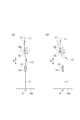
- the functional element layer 15 side of the workpiece 1 is attached to the protective film 22 held by the ring-shaped holding member 20.
- the first modified region 7a and the second modified region 7b are formed along each of the planned cutting lines 5 set in a lattice shape so as to pass between adjacent functional elements. This process will be described in more detail.
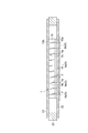
- the first modified region 7a is formed along each of the planned cutting lines 5a. More specifically, the laser beam L1 having a wavelength larger than 1064 nm is condensed on the silicon substrate 10 with the back surface 10b of the silicon substrate 10 as the incident surface, and the surface 10a of the silicon substrate 10 and the first of the laser beam L are condensed.
- the first modified region 7a is formed along the scheduled cutting line 5a by moving the first focused point P1 along the planned cutting line 5a while maintaining the distance to the focused point P1 at the first distance. (First step).
- the distance for offsetting the first condensing point P1 in the direction perpendicular to both the thickness direction of the silicon substrate 10 and the extending direction of the planned cutting line 5a is maintained at zero.
- the first condensing point P1 is moved along the planned cutting line 5a. That is, when viewed from the thickness direction of the silicon substrate 10, the laser beam L is projected along the planned cutting line 5a while maintaining the state where the first condensing point P1 of the laser light L is positioned on the planned cutting line 5a.
- the first condensing point P1 is moved.
- the first modified region 7a is formed inside the silicon substrate 10 along the planned cutting line 5a in a state where the first modified region 7a is positioned on the planned cutting line 5a when viewed from the thickness direction of the silicon substrate 10. .
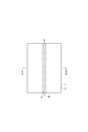
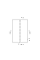
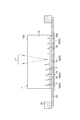
- the second modified region 7b is formed along each of the planned cutting lines 5a. More specifically, the laser beam L1 having a wavelength larger than 1064 nm is condensed on the silicon substrate 10 with the back surface 10b of the silicon substrate 10 as the incident surface, and the second surface 10a and the second laser beam L1 are collected. While the distance from the condensing point P2 is maintained at the second distance larger than the first distance and the second condensing point P2 of the laser light L1 is offset, the second condensing is performed along the scheduled cutting line 5a. By moving the point P2, the second modified region 7b is formed along the planned cutting line 5a (second step).
- the second focused point P ⁇ b> 2 of the laser beam L is maintained along the planned cutting line 5 a while maintaining a state where it is separated from the planned cutting line 5 a by a predetermined distance (cut).
- the second condensing point P2 of the laser light L is moved (parallel to the planned line 5).
- the second modified region 7b is located along the planned cutting line 5a (parallel to the planned cutting line 5a) while being separated from the planned cutting line 5a by a predetermined distance when viewed from the thickness direction of the silicon substrate 10.
- the offset direction of the second condensing point P2 is set as follows. That is, the planned cutting line 5a is set between the effective area 15a and the non-effective area 15b adjacent to each other.
- the effective region 15a side from the position D1 where the first condensing points P1 are combined ( That is, the second condensing point P2 is offset to the opposite side of the non-effective area 15b. That is, the second condensing point P2 is aligned with the position D2 between the position D1 where the first condensing point P1 is combined and the effective region 15a.
- the distance between the position D1 and the position D2 is the offset amount OA.
- the offset amount OA here is, for example, 24 ⁇ m or less (further, for example, 2 ⁇ m or more and 8 ⁇ m or less).
- the crack F extended in the thickness direction of the silicon substrate 10 from the first modified region 7a and the second modified region 7b reaches the surface 10a of the silicon substrate 10, and along the planned cutting line 5a, the functional element
- the layer 15 is cut for each of the effective area 15a and the non-effective area 15b.
- the thickness of the silicon substrate 10 is 775 ⁇ m
- the first modified region 7 a and the second modified region 7 b are formed in a region from the surface 10 a of the silicon substrate 10 to a depth of 160 ⁇ m.
- the first modified region 7a is formed along each of the planned cutting lines 5b. More specifically, the laser beam L1 having a wavelength larger than 1064 nm is condensed on the silicon substrate 10 with the back surface 10b of the silicon substrate 10 as the incident surface, and the surface 10a of the silicon substrate 10 and the first of the laser beam L are condensed.
- the first modified region 7a is formed along the scheduled cutting line 5b by moving the first focused point P1 along the planned cutting line 5b while maintaining the distance to the focused point P1 at the first distance. (Third step).
- the distance for offsetting the first condensing point P1 in the direction perpendicular to both the thickness direction of the silicon substrate 10 and the extending direction of the planned cutting line 5b with respect to the planned cutting line 5b is maintained at zero.
- the first condensing point P1 is moved along the scheduled cutting line 5b. That is, when viewed from the thickness direction of the silicon substrate 10, the laser beam L is projected along the planned cutting line 5b while maintaining the state where the first condensing point P1 of the laser light L is positioned on the planned cutting line 5b.
- the first condensing point P1 is moved. Accordingly, the first modified region 7a is formed inside the silicon substrate 10 along the planned cutting line 5b in a state where the first modified region 7a is positioned on the planned cutting line 5b when viewed from the thickness direction of the silicon substrate 10. .
- the second modified region 7b is formed along each of the planned cutting lines 5b. More specifically, the laser beam L1 having a wavelength larger than 1064 nm is condensed on the silicon substrate 10 with the back surface 10b of the silicon substrate 10 as the incident surface, and the second surface 10a and the second laser beam L1 are collected. While the distance from the condensing point P2 is maintained at the second distance larger than the first distance and the second condensing point P2 of the laser light L1 is offset, the second condensing is performed along the scheduled cutting line 5b. By moving the point P2, the second modified region 7b is formed along the planned cutting line 5b (fourth step).
- the second condensing point P2 of the laser beam L is maintained along the planned cutting line 5b while maintaining a state of being separated from the planned cutting line 5b by a predetermined distance (cut).
- the second condensing point P2 of the laser beam L is moved (in parallel with the planned line 5b).
- the second modified region 7b is located along the planned cutting line 5b (parallel to the planned cutting line 5b) while being separated from the planned cutting line 5b by a predetermined distance when viewed from the thickness direction of the silicon substrate 10.
- the crack F extended in the thickness direction of the silicon substrate 10 from the first modified region 7a and the second modified region 7b reaches the surface 10a of the silicon substrate 10, and along the planned cutting line 5b, the functional element The layer 15 is cut for each effective area 15a.
- the above first to fourth steps are performed by the laser processing apparatus 100 described above. That is, the support 107 supports the workpiece 1.
- the laser light source 101 emits laser light L1 having a wavelength larger than 1064 nm.
- a condensing lens (condensing optical system) 105 is a laser beam emitted from the laser light source 101 onto the workpiece 1 supported by the support 107 so that the back surface 10b of the silicon substrate 10 becomes a laser beam incident surface. L1 is condensed.
- the stage control unit (control unit) 115 and the laser light source control unit (control unit) 102 operate the support base 107 and the laser light source 101, respectively, so that the first to fourth steps described above are performed. Control.
- the movement of the first condensing point P1 and the second condensing point P2 of the laser light L with respect to the scheduled cutting line 5 may be realized by the operation on the condensing lens 105 side, It may be realized by both operations on the optical lens 105 side.
- the workpiece 10 is thinned to a predetermined thickness by polishing the back surface 10 b of the silicon substrate 10.
- the crack F extending in the thickness direction of the silicon substrate 10 from the first modified region 7a and the second modified region 7b reaches the back surface 10b of the silicon substrate 10, and the object 1 is processed into the effective region 15a and the non-processed region 15a. It is cut for each effective area 15b.
- the silicon substrate 10 is thinned to a thickness of 200 ⁇ m.
- the expansion film 23 is attached to the back surface 10 b of the silicon substrate 10 and the holding member 20.
- the protective film 22 is removed.
- the workpiece 1 cut for each of the effective area 15 a and the non-effective area 15 b that is, a plurality of functional elements including a functional element.
- the semiconductor chip 1A and the unnecessary chip 1B are separated from each other.
- the adhesive force of the extension film 23 is reduced by irradiating the extension film 23 with ultraviolet rays, and each semiconductor chip 1A is picked up.
- the back surface 10b of the silicon substrate 10 is polished, as shown in FIG. 27, the back surface 10b of the silicon substrate 10 is polished so that the first modified region 7a and the second modified region 7b remain.
- the back surface 10b of the silicon substrate 10 may be polished so that the first modified region 7a remains and the second modified region 7b does not remain, as shown in FIG.
- the back surface 10b of the silicon substrate 10 may be polished so that the first modified region 7a and the second modified region 7b do not remain.
- the second condensing point P2 of the laser beam L1 is offset in a direction perpendicular to both of the extending directions. Thereby, it can suppress that damage (splash S) arises in the surface 10a of the workpiece 1 on the opposite side to the incident surface of the laser beam L1.
- the second condensing point P2 is offset to the effective region 15a side from the position where the first condensing point P1 is combined.
- the position where the splash S can occur with respect to the surface 10a of the workpiece 1 opposite to the incident surface of the laser beam L1 can be shifted to the non-effective region 15b side. That is, the position where the splash S can occur can be controlled to a position that does not affect the characteristics of the functional element. From the above viewpoint, according to the laser processing method and the laser processing apparatus 100 according to the embodiment, it is possible to suppress the deterioration of the characteristics of the functional elements.
- the first modified region 7a and the second modified region 7b are formed in comparison with the case where the laser beam L0 having a wavelength of 1064 nm or less is used.
- the crack F can be greatly extended in the thickness direction of the silicon substrate 10 from the first modified region 7a and the second modified region 7b.
- the laser beam L1 having a wavelength of 1099 ⁇ m or more and 1342 ⁇ m or less silicon is removed from the first modified region 7a and the second modified region 7b along with the formation of the first modified region 7a and the second modified region 7b.
- the crack F can be extended more in the thickness direction of the substrate 10.
- the laser beam L1 having a wavelength of 1342 ⁇ m can extend the crack F more greatly.
- the offset amount for offsetting the second condensing point P2 of the laser beam L1 when forming the second modified region 7b is set to 24 ⁇ m or less, the gap between the first modified region 7a and the second modified region 7b is set.
- the crack F is securely connected, and the first modified region 7a and the second modified region 7b are cracked in the thickness direction of the silicon substrate 10 with the formation of the first modified region 7a and the second modified region 7b. F can be extended reliably.
- the offset amount is 4 ⁇ m or more and 18 ⁇ m or less, the crack F is more reliably connected between the first modified region 7a and the second modified region 7b, and the first modified region 7a and the second modified region are connected.
- the crack F can be more reliably extended from the region 7b in the thickness direction of the silicon substrate 10.
- the offset amount is 6 ⁇ m or more and 16 ⁇ m or less, the suppression of the occurrence of the splash S and the connection and extension of the crack F can be realized in a well-balanced manner.
- the splash S may be generated on the side opposite to the side where the second focusing point P2 of the laser beam L1 is offset when the second modified region 7b is formed. Therefore, in the case where the second modified region 7b is formed along the scheduled cutting line 5a set between the effective region 15a and the non-effective region 15b (second step), the offset direction is set as described above. By doing so, the position where the splash S can occur can be controlled to the non-effective area 15b side. For this reason, in suppressing the characteristic deterioration of the functional element, the demand for suppressing the occurrence of the splash S is relatively low.
- the offset amount OA of the second focusing point P2 is necessary and sufficient in the range of 24 ⁇ m or less, particularly in the range of 2 ⁇ m or more and 8 ⁇ m or less. According to this, since the offset distance between the first modified region 7a and the second modified region 7b is also relatively small, the step of the cut surface is also small.
- both sides of the planned cutting line 5b are on the effective region 15a. Therefore, there is a relatively high demand for suppressing the occurrence of the splash S itself. Therefore, in this case, in the range of 24 ⁇ m or less, in particular, the range of 4 ⁇ m or more and 18 ⁇ m or less can be obtained.
- the thickness direction of the silicon substrate 10 with respect to the planned cutting line 5 (scheduled cutting lines 5a and 5b).
- the first distance of the laser light L1 along the planned cutting line 5 is maintained while maintaining the distance for offsetting the first condensing point P1 of the laser light L1 in the direction perpendicular to both the extending directions of the planned cutting line 5.
- the condensing point P1 is moved. Thereby, the crack F extending from the first modified region 7 a to the surface 10 a side of the silicon substrate 10 can be aligned on the planned cutting line 5.
- one embodiment of one aspect of the present invention has been described.
- one aspect of the present invention is not limited to the above-described embodiment, and may be modified or changed without departing from the scope described in each claim.
- the first condensing point P1 of the light L1 is offset and the second modified region 7b is formed, the thickness direction of the silicon substrate 10 and the extending direction of the planned cutting line 5 are changed with respect to the planned cutting line 5.
- the second condensing point P2 of the laser light L1 may be offset to the other side in the direction perpendicular to both directions. That is, when the first modified region 7a is formed, when viewed from the thickness direction of the silicon substrate 10, the first condensing point P1 of the laser light L is separated from the planned cutting line 5 to one side by a predetermined distance. The first focused point P1 of the laser beam L is moved along the planned cutting line 5 (in parallel with the planned cutting line 5) while forming the second modified region 7b while maintaining the above-described state.
- the second condensing point P ⁇ b> 2 of the laser beam L is maintained along the planned cutting line 5 while maintaining a state where it is separated from the planned cutting line 5 to the other side by a predetermined distance (You may move the 2nd condensing point P2 of the laser beam L (parallel to the cutting scheduled line 5).
- the first modified region 7a is formed along the planned cutting line 5 (scheduled to be cut) in a state where it is separated from the planned cutting line 5 to one side by a predetermined distance when viewed from the thickness direction of the silicon substrate 10.
- the second modified region 7b is formed in the silicon substrate 10 (in parallel with the line 5), and the second modified region 7b is separated from the planned cutting line 5 to the other side by a predetermined distance when viewed from the thickness direction of the silicon substrate 10. Thus, it is formed inside the silicon substrate 10 along the planned cutting line 5 (in parallel with the planned cutting line 5). In this case, the first modified region 7a and the second modified region 7b can be formed in a well-balanced manner on one side and the other side with respect to the planned cutting line 5.
- the formation process (second process) of the second modified region 7b was performed on the planned cutting line 5a extending in the second direction.
- region 7a is implemented with respect to the cutting scheduled line 5b extended in a 1st direction among all the cutting planned lines 5 set to the grid
- the execution order of the first to fourth steps is not limited to this example.
- the formation process (first process and third process) of the first modified region 7a is performed on all the planned cutting lines 5 (scheduled cutting lines 5a and 5b) set in a lattice shape, and then You may implement the formation process (2nd process and 4th process) of the 2nd modification area
- region 7a is implemented for every one scheduled cutting line 5 with respect to the several scheduled cutting line 5, and after that, 2nd You may implement the formation process (2nd process or 4th process) of the modification area
- the workpiece 1 may be provided with a semiconductor substrate made of another semiconductor material instead of the silicon substrate 10.
- the wavelength of the laser beam L1 is not necessarily larger than 1064 ⁇ m (for example, it may be 1064 ⁇ m).
- the back surface 10b of the silicon substrate 10 is polished after the first modified region 7a formation step (first step and third step) and the second modified region 7b formation step (second step and fourth step). You don't have to.
- the thickness of the workpiece 1 is relatively small with respect to the number of the modified regions 7 formed per one scheduled cutting line 5, or one for the thickness of the workpiece 1
- the workpiece 1 can be turned into the planned cutting line 5 without polishing the back surface 10b of the silicon substrate 10. Can be cut along.
- SYMBOLS 1 Processing target object, 5, 5a, 5b ... Planned cutting line, 7a ... 1st modified region, 7b ... 2nd modified region, 10 ... Silicon substrate (semiconductor substrate), 10a ... Front surface, 10b ... Back surface, 15a ... Effective area, 15b ... Non-effective area, 100 ... Laser processing apparatus, 101 ... Laser light source, 102 ... Laser light source controller (control part), 105 ... Condensing lens (condensing optical system), 107 ... Support stand, 115: Stage control unit (control unit), L1: Laser beam, P1: First focusing point, P2: Second focusing point.
Landscapes
- Physics & Mathematics (AREA)
- Optics & Photonics (AREA)
- Engineering & Computer Science (AREA)
- Plasma & Fusion (AREA)
- Mechanical Engineering (AREA)
- Chemical & Material Sciences (AREA)
- Chemical Kinetics & Catalysis (AREA)
- General Chemical & Material Sciences (AREA)
- Oil, Petroleum & Natural Gas (AREA)
- Laser Beam Processing (AREA)
- Dicing (AREA)
Abstract
Description
Claims (7)
- 表面及び裏面を有する半導体基板と、前記表面上に形成された複数の有効領域と、前記有効領域の間において前記表面上に形成された非有効領域と、を有する加工対象物に、前記裏面を入射面としてレーザ光を集光させ、前記表面と前記レーザ光の第1集光点との距離を第1距離に維持しつつ、隣り合う前記有効領域と前記非有効領域との間を通るように設定された切断予定ラインに沿って前記第1集光点を移動させることで、前記切断予定ラインに沿って第1改質領域を形成する第1工程と、
前記第1工程の後に、前記加工対象物に、前記裏面を入射面として前記レーザ光を集光させて、前記表面と前記レーザ光の第2集光点との距離を前記第1距離よりも大きい第2距離に維持しつつ、前記切断予定ラインに沿って前記第2集光点を移動させることで、前記切断予定ラインに沿って第2改質領域を形成する第2工程と、
を備え、
前記有効領域は、機能素子を含み、
前記第2工程においては、前記半導体基板の厚さ方向及び前記切断予定ラインの延在方向の両方向に垂直な方向について、前記第1集光点を合わせた位置よりも前記有効領域側に前記第2集光点をオフセットさせつつ、前記切断予定ラインに沿って前記第2集光点を移動させる、
レーザ加工方法。 - 前記半導体基板は、シリコン基板であり、
前記レーザ光は、1064nmよりも大きい波長を有する、
請求項1に記載のレーザ加工方法。 - 前記レーザ光は、1099μm以上1342μm以下の波長を有する、
請求項2に記載のレーザ加工方法。 - 前記第1集光点を合わせた位置に対して、前記半導体基板の前記厚さ方向及び前記切断予定ラインの前記延在方向の両方向に垂直な前記方向に前記第2集光点をオフセットさせる距離は、24μm以下である、
請求項1~3のいずれか一項に記載のレーザ加工方法。 - 前記第1集光点を合わせた位置に対して、前記半導体基板の前記厚さ方向及び前記切断予定ラインの前記延在方向の両方向に垂直な前記方向に前記第2集光点をオフセットさせる前記距離は、2μm以上8μm以下である、
請求項4に記載のレーザ加工方法。 - 前記第1工程において、前記切断予定ラインに対して、前記半導体基板の前記厚さ方向及び前記切断予定ラインの前記延在方向の両方向に垂直な前記方向に前記第1集光点をオフセットさせる距離を0に維持しつつ、前記切断予定ラインに沿って前記第1集光点を移動させる、
請求項1~5のいずれか一項記載のレーザ加工方法。 - 表面及び裏面を有する半導体基板と、前記表面上に形成された複数の有効領域と、前記有効領域の間において前記表面上に形成された非有効領域と、を有する加工対象物を支持する支持台と、
レーザ光を出射するレーザ光源と、
前記裏面が入射面となるように前記支持台に支持された前記加工対象物に、前記レーザ光源から出射された前記レーザ光を集光する集光光学系と、
前記支持台、前記レーザ光源及び前記集光光学系の少なくとも1つの動作を制御する制御部と、を備え、
前記有効領域は、機能素子を含み、
前記制御部は、前記表面と前記レーザ光の第1集光点との距離を第1距離に維持しつつ、隣り合う前記有効領域と前記非有効領域との間を通るように設定された切断予定ラインに沿って前記第1集光点を移動させ、その後に、前記表面と前記レーザ光の第2集光点との距離を前記第1距離よりも大きい第2距離に維持しつつ、且つ、前記半導体基板の厚さ方向及び前記切断予定ラインの延在方向の両方向に垂直な方向について前記第1集光点を合わせた位置よりも前記有効領域側に前記第2集光点をオフセットさせつつ、前記切断予定ラインに沿って前記第2集光点を移動させる、
レーザ加工装置。
Priority Applications (4)
| Application Number | Priority Date | Filing Date | Title |
|---|---|---|---|
| DE112016004432.1T DE112016004432T5 (de) | 2015-09-29 | 2016-08-09 | Laserbearbeitungsverfahren und Laserbearbeitungsvorrichtung |
| KR1020187009546A KR102605404B1 (ko) | 2015-09-29 | 2016-08-09 | 레이저 가공 방법 및 레이저 가공 장치 |
| US15/763,915 US11103959B2 (en) | 2015-09-29 | 2016-08-09 | Laser processing method, and laser processing device |
| CN201680056478.3A CN108136539B (zh) | 2015-09-29 | 2016-08-09 | 激光加工方法及激光加工装置 |
Applications Claiming Priority (2)
| Application Number | Priority Date | Filing Date | Title |
|---|---|---|---|
| JP2015-191096 | 2015-09-29 | ||
| JP2015191096A JP6542630B2 (ja) | 2015-09-29 | 2015-09-29 | レーザ加工方法及びレーザ加工装置 |
Publications (1)
| Publication Number | Publication Date |
|---|---|
| WO2017056744A1 true WO2017056744A1 (ja) | 2017-04-06 |
Family
ID=58423296
Family Applications (1)
| Application Number | Title | Priority Date | Filing Date |
|---|---|---|---|
| PCT/JP2016/073468 Ceased WO2017056744A1 (ja) | 2015-09-29 | 2016-08-09 | レーザ加工方法及びレーザ加工装置 |
Country Status (7)
| Country | Link |
|---|---|
| US (1) | US11103959B2 (ja) |
| JP (1) | JP6542630B2 (ja) |
| KR (1) | KR102605404B1 (ja) |
| CN (1) | CN108136539B (ja) |
| DE (1) | DE112016004432T5 (ja) |
| TW (1) | TWI706823B (ja) |
| WO (1) | WO2017056744A1 (ja) |
Families Citing this family (4)
| Publication number | Priority date | Publication date | Assignee | Title |
|---|---|---|---|---|
| DE102017212858B4 (de) * | 2017-07-26 | 2024-08-29 | Disco Corporation | Verfahren zum Bearbeiten eines Substrats |
| JP2019051529A (ja) * | 2017-09-13 | 2019-04-04 | 東芝メモリ株式会社 | 半導体製造装置 |
| JP7436219B2 (ja) * | 2020-01-27 | 2024-02-21 | 浜松ホトニクス株式会社 | レーザ加工装置、及び、レーザ加工方法 |
| US12440925B2 (en) | 2020-07-15 | 2025-10-14 | Hamamatsu Photonics K.K. | Laser machining apparatus, laser machining method, and method for manufacturing semiconductor member |
Citations (3)
| Publication number | Priority date | Publication date | Assignee | Title |
|---|---|---|---|---|
| JP2013048207A (ja) * | 2011-07-27 | 2013-03-07 | Toshiba Mach Co Ltd | レーザダイシング方法 |
| JP2014087806A (ja) * | 2012-10-29 | 2014-05-15 | Mitsuboshi Diamond Industrial Co Ltd | レーザー加工装置、および、パターン付き基板の加工条件設定方法 |
| JP2015130470A (ja) * | 2013-12-05 | 2015-07-16 | 豊田合成株式会社 | Iii族窒化物半導体発光素子およびその製造方法 |
Family Cites Families (12)
| Publication number | Priority date | Publication date | Assignee | Title |
|---|---|---|---|---|
| CN101335235B (zh) * | 2002-03-12 | 2010-10-13 | 浜松光子学株式会社 | 基板的分割方法 |
| JP2008147412A (ja) | 2006-12-11 | 2008-06-26 | Matsushita Electric Ind Co Ltd | 半導体ウェハ,半導体装置及び半導体ウェハの製造方法ならびに半導体装置の製造方法 |
| JP2009124077A (ja) * | 2007-11-19 | 2009-06-04 | Denso Corp | 半導体チップ及びその製造方法 |
| JP5632751B2 (ja) * | 2009-02-09 | 2014-11-26 | 浜松ホトニクス株式会社 | 加工対象物切断方法 |
| JP2013089714A (ja) | 2011-10-17 | 2013-05-13 | Disco Abrasive Syst Ltd | チップ形成方法 |
| JP2013126682A (ja) | 2011-11-18 | 2013-06-27 | Hamamatsu Photonics Kk | レーザ加工方法 |
| WO2013156891A1 (en) * | 2012-04-16 | 2013-10-24 | Koninklijke Philips N.V. | Method and apparatus for creating a w-mesa street |
| JP2014041924A (ja) * | 2012-08-22 | 2014-03-06 | Hamamatsu Photonics Kk | 加工対象物切断方法 |
| JP2014041925A (ja) | 2012-08-22 | 2014-03-06 | Hamamatsu Photonics Kk | 加工対象物切断方法 |
| JP6062315B2 (ja) * | 2013-04-24 | 2017-01-18 | 株式会社ディスコ | ウエーハの加工方法 |
| JP6301726B2 (ja) * | 2014-05-07 | 2018-03-28 | 株式会社ディスコ | 光デバイスの加工方法 |
| JP6308919B2 (ja) * | 2014-09-03 | 2018-04-11 | 株式会社ディスコ | ウエーハの加工方法 |
-
2015
- 2015-09-29 JP JP2015191096A patent/JP6542630B2/ja active Active
-
2016
- 2016-08-09 CN CN201680056478.3A patent/CN108136539B/zh active Active
- 2016-08-09 DE DE112016004432.1T patent/DE112016004432T5/de active Pending
- 2016-08-09 WO PCT/JP2016/073468 patent/WO2017056744A1/ja not_active Ceased
- 2016-08-09 US US15/763,915 patent/US11103959B2/en active Active
- 2016-08-09 KR KR1020187009546A patent/KR102605404B1/ko active Active
- 2016-08-17 TW TW105126244A patent/TWI706823B/zh active
Patent Citations (3)
| Publication number | Priority date | Publication date | Assignee | Title |
|---|---|---|---|---|
| JP2013048207A (ja) * | 2011-07-27 | 2013-03-07 | Toshiba Mach Co Ltd | レーザダイシング方法 |
| JP2014087806A (ja) * | 2012-10-29 | 2014-05-15 | Mitsuboshi Diamond Industrial Co Ltd | レーザー加工装置、および、パターン付き基板の加工条件設定方法 |
| JP2015130470A (ja) * | 2013-12-05 | 2015-07-16 | 豊田合成株式会社 | Iii族窒化物半導体発光素子およびその製造方法 |
Also Published As
| Publication number | Publication date |
|---|---|
| KR102605404B1 (ko) | 2023-11-24 |
| US20180281116A1 (en) | 2018-10-04 |
| DE112016004432T5 (de) | 2018-07-05 |
| CN108136539A (zh) | 2018-06-08 |
| TW201718153A (zh) | 2017-06-01 |
| JP2017069309A (ja) | 2017-04-06 |
| TWI706823B (zh) | 2020-10-11 |
| US11103959B2 (en) | 2021-08-31 |
| CN108136539B (zh) | 2020-05-22 |
| KR20180057643A (ko) | 2018-05-30 |
| JP6542630B2 (ja) | 2019-07-10 |
Similar Documents
| Publication | Publication Date | Title |
|---|---|---|
| JP6605278B2 (ja) | レーザ加工方法 | |
| JP5491761B2 (ja) | レーザ加工装置 | |
| CN100485901C (zh) | 基板的分割方法 | |
| JP6605277B2 (ja) | レーザ加工方法及びレーザ加工装置 | |
| WO2017056744A1 (ja) | レーザ加工方法及びレーザ加工装置 | |
| JP6876098B2 (ja) | レーザ加工装置 | |
| JP6752232B2 (ja) | 加工対象物切断方法 | |
| JP2013118413A (ja) | Ledチップ | |
| JP2013118277A (ja) | Ledパターン付き基板の加工方法 | |
| JP2011134799A (ja) | 半導体装置の製造方法 |
Legal Events
| Date | Code | Title | Description |
|---|---|---|---|
| 121 | Ep: the epo has been informed by wipo that ep was designated in this application |
Ref document number: 16850921 Country of ref document: EP Kind code of ref document: A1 |
|
| WWE | Wipo information: entry into national phase |
Ref document number: 15763915 Country of ref document: US |
|
| WWE | Wipo information: entry into national phase |
Ref document number: 112016004432 Country of ref document: DE |
|
| ENP | Entry into the national phase |
Ref document number: 20187009546 Country of ref document: KR Kind code of ref document: A |
|
| 122 | Ep: pct application non-entry in european phase |
Ref document number: 16850921 Country of ref document: EP Kind code of ref document: A1 |