WO2017056720A1 - 能動素子、および能動素子の製造方法 - Google Patents
能動素子、および能動素子の製造方法 Download PDFInfo
- Publication number
- WO2017056720A1 WO2017056720A1 PCT/JP2016/073001 JP2016073001W WO2017056720A1 WO 2017056720 A1 WO2017056720 A1 WO 2017056720A1 JP 2016073001 W JP2016073001 W JP 2016073001W WO 2017056720 A1 WO2017056720 A1 WO 2017056720A1
- Authority
- WO
- WIPO (PCT)
- Prior art keywords
- electrode
- organic semiconductor
- active element
- semiconductor layer
- conductive layer
- Prior art date
- Legal status (The legal status is an assumption and is not a legal conclusion. Google has not performed a legal analysis and makes no representation as to the accuracy of the status listed.)
- Ceased
Links
Images














Classifications
-
- H—ELECTRICITY
- H10—SEMICONDUCTOR DEVICES; ELECTRIC SOLID-STATE DEVICES NOT OTHERWISE PROVIDED FOR
- H10K—ORGANIC ELECTRIC SOLID-STATE DEVICES
- H10K10/00—Organic devices specially adapted for rectifying, amplifying, oscillating or switching; Organic capacitors or resistors having potential barriers
- H10K10/40—Organic transistors
-
- H—ELECTRICITY
- H10—SEMICONDUCTOR DEVICES; ELECTRIC SOLID-STATE DEVICES NOT OTHERWISE PROVIDED FOR
- H10D—INORGANIC ELECTRIC SEMICONDUCTOR DEVICES
- H10D30/00—Field-effect transistors [FET]
- H10D30/60—Insulated-gate field-effect transistors [IGFET]
- H10D30/67—Thin-film transistors [TFT]
-
- H—ELECTRICITY
- H10—SEMICONDUCTOR DEVICES; ELECTRIC SOLID-STATE DEVICES NOT OTHERWISE PROVIDED FOR
- H10D—INORGANIC ELECTRIC SEMICONDUCTOR DEVICES
- H10D64/00—Electrodes of devices having potential barriers
- H10D64/01—Manufacture or treatment
- H10D64/011—Manufacture or treatment of electrodes ohmically coupled to a semiconductor
Definitions
- the present invention relates to an active element using an organic semiconductor for a semiconductor layer.
- Non-Patent Document 1 As an electrode material of an active element using an organic semiconductor, Au having a small energy barrier with the organic semiconductor and high conductivity is used (see, for example, Non-Patent Document 1).
- an object of the present invention is to provide an active element capable of ensuring a necessary operation speed while suppressing material costs, and a method for manufacturing the active element.
- the present inventor has examined an electrode material as a substitute for Au.
- an electrode material Cu, which has high conductivity and can be obtained at low cost, is suitable for industrial production.
- Cu has a problem in obtaining high carrier injection efficiency because of its relatively high energy barrier with an organic semiconductor. . Therefore, the present inventor has come up with the idea that the electrode has a laminated structure by combining a plurality of materials while studying an electrode material having performance equivalent to that of Au while suppressing the material cost.
- a material having a high carrier injection efficiency is used for the lower electrode that is easily in contact with the organic semiconductor layer, and the upper electrode is less likely to be in contact with the organic semiconductor layer than the lower electrode. Found that a material having high conductivity was used.
- the active element of the present invention that can achieve the above-described object comprises: a base material; a lower first electrode formed on one main surface of the base material, and an upper first electrode formed on the lower first electrode.
- An energy barrier between the upper first electrode and the organic semiconductor layer is higher than an energy barrier between the lower first electrode and the organic semiconductor layer; between the upper second electrode and the organic semiconductor layer
- the energy barrier is higher than the energy barrier between the lower second electrode and the organic semiconductor layer;
- the conductivity of the upper first electrode is lower Higher than the conductivity of the first electrode; conductivity of the upper second electrode, being higher than the conductivity of the lower second electrode.
- the active device of the present invention has a lower first electrode-organic semiconductor layer lower than the carrier injection efficiency of the upper first electrode-organic semiconductor layer.
- the carrier injection efficiency is high, and the carrier injection efficiency of the lower second electrode-organic semiconductor layer is higher than the carrier injection efficiency of the upper second electrode-organic semiconductor layer.
- the lower first electrode and the lower second electrode disposed on the lower side are likely to exchange charges with the organic semiconductor layer.
- the conductivity of the upper first electrode is higher than the conductivity of the lower first electrode, and the conductivity of the upper second electrode is higher than the conductivity of the lower second electrode. is there.
- the active element of the present invention has a laminated structure of the first electrode and the second electrode, and the electrode material and shape can be designed independently on the upper side and the lower side. It is possible to achieve both possibilities.
- At least a part of the upper first electrode is arranged inside the lower first electrode, and in the surface direction of the base material, at least a part of the upper second electrode is lower side. It is preferable that it is arranged inside the second electrode. If at least a part of the upper first electrode is disposed on the inner side of the lower first electrode, the contact area between the lower first electrode and the organic semiconductor layer can be increased, and from the electrode to the organic semiconductor layer Since carriers are efficiently injected, the operating speed of the active device can be increased. The same applies to the lower second electrode and the upper second electrode.
- the distance from the end of the lower first electrode to the end of the upper first electrode is 1 nm or more and 20 ⁇ m or less in the surface direction of the substrate, and the distance from the end of the lower second electrode to the end of the upper second electrode is The surface direction of the substrate is preferably 1 nm or more and 20 ⁇ m or less.
- the organic semiconductor layer is on the lower first electrode, between the end of the lower first electrode and the end of the upper first electrode, and on the lower second electrode and on the lower side. It is preferable to arrange between the end of the second electrode and the end of the upper second electrode. This increases the contact area between the lower first electrode and the organic semiconductor layer, and the lower second electrode and the organic semiconductor layer, so that charge transfer is facilitated.
- At least a part of the upper first electrode is disposed between the lower first electrode and the organic semiconductor layer, and at least a part of the upper second electrode is the lower second electrode and the organic semiconductor. It is preferred that they are arranged between the layers. This can increase the contact area between the organic semiconductor layer and the lower first electrode, and between the organic semiconductor layer and the lower second electrode. In addition, the contact area between the upper electrode and the organic semiconductor layer also increases, and it becomes easy to transfer and receive charges, so that the number of carriers contributing to the operation of the active element can be increased, and the operation speed of the active element is increased. .
- Each of the upper first electrode, the lower first electrode, the upper second electrode, and the lower second electrode includes an electrode portion and a wiring portion that is formed narrower than the electrode portion.
- the electrode portion of the upper first electrode is disposed inside the electrode portion of the lower first electrode, and the electrode portion of the upper second electrode is on the lower side in the surface direction of the substrate. It is preferable that it is arrange
- the region sandwiched between the first electrode and the second electrode meanders.
- the contact length between the first electrode and the organic semiconductor layer or between the second electrode and the organic semiconductor layer is increased, so that the current flowing between the first electrode and the second electrode can be increased.
- the material of the lower first electrode and the lower second electrode is ITO
- the material of the upper first electrode and the upper second electrode is Cu. This is because ITO has a low energy barrier between the organic semiconductor layer and the carrier injection efficiency into the organic semiconductor layer is high. Since Cu has a high conductivity, it contributes to an improvement in the operating speed of the active element. Further, since Cu is inexpensive, the productivity of active elements can be increased.
- a top-gate transistor can be formed.
- a transistor in which the base material also serves as the gate insulating film can be configured.
- the method of manufacturing an active element of the present invention includes: a step of forming a first conductive layer on one main surface of a substrate; and a step of forming a second conductive layer on the first conductive layer; A step of forming a mask layer on the second conductive layer; a region where the first conductive layer and the second conductive layer are brought into contact with the etching solution and are not covered with the mask layer of the first conductive layer and the second conductive layer; The first electrode having the lower first electrode and the upper first electrode on the lower first electrode, the lower second electrode, and the lower second electrode on one main surface of the base material And a second electrode disposed adjacent to the first electrode; on one main surface of the substrate, and at least a first electrode Forming an organic semiconductor layer so as to cover a region between the electrode and the second electrode; and an energy between the second conductive layer and the organic semiconductor layer.
- Ghee barrier is higher than the energy barrier between the first conductive layer and the organic semiconductor layer; the conductivity of the second conductive layer, being higher than the conductivity of the first conductive layer.
- the lower first electrode, the upper first electrode, the lower second electrode, and the upper second electrode can be formed together, the positional deviation of the upper first electrode with respect to the lower first electrode, The positional deviation of the upper second electrode with respect to the lower second electrode is suppressed.
- the organic semiconductor layer Before forming the organic semiconductor layer, it is preferable to include a step of bringing the first electrode and the second electrode into contact with another etching solution to remove at least a partial region of the upper first electrode and the upper second electrode. Accordingly, since the upper first electrode and the upper second electrode can be side-etched without performing another mask layer formation and peeling step, at least one of the upper first electrode in the surface direction of the base material.
- the active element 1 is obtained in which the portion is disposed on the inner side of the lower first electrode, and at least a part of the upper second electrode is disposed on the inner side of the lower second electrode.
- the active element of the present invention since the carrier injection efficiency of the lower first electrode and the lower second electrode is high, charges are easily transferred to and from the organic semiconductor layer. Since the electric conduction from the electrode arranged on the electrode to the electrode arranged on the lower side is facilitated, the operation speed can be increased. In this way, by adopting a laminated structure in which the electrode material and shape can be designed independently on the upper side and the lower side, it is possible to achieve both good operating characteristics and the possibility of selecting an inexpensive material.
- the lower first electrode, the upper first electrode, the lower second electrode, and the upper second electrode can be formed together. The positional deviation of the first electrode and the positional deviation of the upper second electrode with respect to the lower second electrode are suppressed.
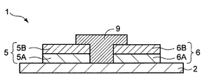
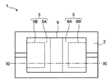
- FIG. 1 represents a plan view of an active device of the present invention.
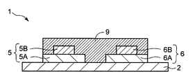
- FIG. 2 is a sectional view of the active element shown in FIG. 1 taken along the line II-II.
- FIG. 3 is a sectional view of the active element shown in FIG. 1 taken along the line III-III.
- the modification of the top view of the active element shown in FIG. 1 is represented.
- FIG. 5 is a VV sectional view of the active element shown in FIG. 4.
- FIG. 6 is a cross-sectional view taken along line VI-VI of the active element shown in FIG. 4.
- the modification of the top view of the active element shown in FIG. 4 is represented.
- FIG. 8 is a sectional view of the active element shown in FIG. 7 taken along the line VIII-VIII.
- FIG. 8 illustrates a cross-sectional view of the active element IX-IX shown in FIG. 7.
- the modification of the top view of the active element shown in FIG. 7 is represented.
- XI-XI sectional drawing of the active element shown in FIG. 10 is represented.
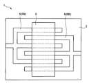
- the modification of the top view of the active element shown in FIG. 1 is represented.
- the modification of the top view of the active element shown in FIG. 4 is represented.
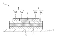
- 6 shows a modification of the cross-sectional view of the active element shown in FIG. 6 shows a modification of the cross-sectional view of the active element shown in FIG. 6 shows a modification of the cross-sectional view of the active element shown in FIG.
- the process sectional drawing of the manufacturing method of the active element of this invention is represented.
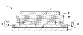
- FIG. 3 is a cross-sectional view of an active element according to an embodiment.
- FIG. 3 is a cross-sectional view of an active element according to an embodiment. Sectional drawing of the active element which concerns on a comparative example is represented. Sectional drawing of the active element which concerns on a comparative example is represented. 3 is a graph showing gate voltage-drain current characteristics of an active element.
- the present invention will be described more specifically on the basis of the embodiments.
- the present invention is not limited by the following embodiments, but may be implemented with modifications within a range that can meet the purpose described above and below. Of course, any of these is also included in the technical scope of the present invention.
- the dimensional ratios of the various members in the drawings are given priority to contribute to the understanding of the characteristics of the present invention, and may be different from the actual dimensional ratios.
- an active element is an element that performs signal amplification and rectification, and is, for example, a semiconductor element such as a transistor, a thyristor, or a diode. Examples of these applications include displays, touch panels, solar cells, semiconductor lasers, pressure sensors, and biosensors.
- the active element has a thickness direction and a surface direction.
- the thickness direction of the active element is a direction in which the base material, the first electrode, the second electrode, and the organic semiconductor layer are laminated, and the surface direction of the active element is a direction orthogonal to the thickness direction.
- FIG. 1 is a plan view of the active element of the present invention
- FIG. 2 is a sectional view taken along the line II-II of the active element shown in FIG. 1
- FIG. 3 is a cross-sectional view of the active element shown in FIG. A sectional view is shown.
- the active element 1 of the present invention includes a base material 2, a first electrode 5 including a lower first electrode 5A and an upper first electrode 5B, a lower second electrode 6A, The second electrode 6 including the upper second electrode 6B and the organic semiconductor layer 9 are included.
- the base material 2 has one main surface and the other main surface, and is provided to support the first electrode 5, the second electrode 6, and the organic semiconductor layer 9.
- a flexible substrate made of a polymer film such as polyethylene naphthalate (PEN), polyethylene terephthalate (PET), polyimide (PI), or a rigid substrate such as a glass substrate is preferably used.
- PEN polyethylene naphthalate
- PET polyethylene terephthalate
- PI polyimide
- a rigid substrate such as a glass substrate
- the thickness of the base material 2 is preferably, for example, 5 ⁇ m or more, more preferably 10 ⁇ m or more, and further preferably 18 ⁇ m or more.
- the thickness of the substrate 2 is preferably 200 ⁇ m or less, preferably 150 ⁇ m or less, and more preferably 125 ⁇ m or less.
- the thickness of the substrate 2 is preferably 10 ⁇ m or less, more preferably 7 ⁇ m or less, and 5 ⁇ m or less. More preferably, it is preferably 0.1 ⁇ m or more, more preferably 0.5 ⁇ m or more, and further preferably 1 ⁇ m or more.
- the organic semiconductor layer 9 is formed on one main surface of the base material 2 so as to cover at least a region between the first electrode 5 and the second electrode 6. .
- the organic semiconductor layer 9 functions as a channel region.
- a material of the organic semiconductor layer 9 for example, pentacene, anthracene, tetracene, rubrene, dinaphthothienothiophene, polyacetylene, polythiophene, fullerene, carbon nanotube, or the like can be used.
- the upper limit of the thickness of the organic semiconductor layer 9 is not particularly limited, but in order to obtain a thin active element 1, the thickness of the organic semiconductor layer 9 is preferably 200 nm or less, and more preferably 150 nm or less, for example. Preferably, it is 100 nm or less.
- the organic semiconductor layer 9 is preferably formed by a vacuum deposition method or a printing method. Specifically, in the printing method, a mixed liquid (hereinafter referred to as “organic semiconductor ink”) in which organic semiconductor molecules are dispersed in an organic solvent for coating is applied to the substrate 2 and then dried. Is done.
- organic semiconductor ink a mixed liquid in which organic semiconductor molecules are dispersed in an organic solvent for coating
- the organic semiconductor layer 9 is formed by a printing method, for example, mesitylene, toluene, chloroform, p-diisopropylbenzene, benzyl alcohol, or a mixed solvent thereof can be used as the organic solvent.
- the active element 1 of the present invention has a first electrode 5 and a second electrode 6 formed adjacent to each other on one main surface of a substrate 2.
- the first electrode 5, the second electrode 6, and a third electrode to be described later are electrically connected to operate the active element 1, for example,
- the active element 1 is a transistor
- the first electrode 5 corresponds to a source electrode
- the second electrode 6 corresponds to a drain electrode
- the third electrode 11 corresponds to a gate electrode.
- the electrode material can be a conductive material, for example, a metal material such as Cu, Al, Ag, Ni, Au, a metal oxide such as ITO, ZnO, IGO, IGZO, CuO, C, carbon nanotube, graphite Carbon materials such as graphene can be used.
- a metal material such as Cu, Al, Ag, Ni, Au
- a metal oxide such as ITO, ZnO, IGO, IGZO, CuO, C
- carbon nanotube graphite Carbon materials such as graphene can be used.
- the electrode can be formed by, for example, a photolithography method or a printing method. From the viewpoint of improving the accuracy of the relative positions of the first electrode 5 and the second electrode 6, the first electrode 5 and the second electrode 6 are preferably formed by a photolithography method.
- the thickness of the electrode is, for example, preferably 5 nm or more, more preferably 10 nm or more, and further preferably 20 nm or more in order to ensure the necessary electrical conductivity.
- the upper limit of the thickness of the electrode is not particularly limited, but is preferably 1 ⁇ m or less, for example, from the viewpoint of suppressing an increase in the total thickness of the active element 1 and shortening the etching time when using a photolithography method, It is more preferably 700 nm or less, and further preferably 500 nm or less.
- the first electrode 5 and the second electrode 6 may be formed adjacent to each other, and one side of the first electrode 5 and one side of the second electrode 6 may be arranged to face each other.
- the one side 5C of the first electrode 5 and the one side 6C of the second electrode 6 are arranged to face each other.
- the first electrode 5 includes a lower first electrode 5A formed on one main surface of the substrate 2, and an upper side formed on the lower first electrode 5A. And a first electrode 5B.
- the second electrode 6 includes a lower second electrode 6A formed on one main surface of the substrate 2 and an upper second electrode formed on the lower second electrode 6A. And an electrode 6B.
- the first electrode 5 and the second electrode 6 have a laminated structure, and the electrode material and shape can be designed independently on the upper side and the lower side, so that it is possible to select good operating characteristics and inexpensive materials. It can be compatible with sex.
- the lower first electrode 5A and the lower second electrode 6A (hereinafter sometimes collectively referred to as “lower electrode”) disposed on the lower side are the upper first electrodes disposed on the upper side.
- the contact area with the organic semiconductor layer 9 tends to be large.
- charge carriers (hereinafter simply referred to as “carriers”) are injected from the electrode to the organic semiconductor layer 9 or from the organic semiconductor layer 9 to the electrode.
- the upper electrode mainly has a role of transferring charges to and from the lower electrode or external wiring (not shown).
- the upper electrode and the lower electrode are formed from different materials. Further, as described later in “2. Active device manufacturing method”, the lower first electrode 5A and the lower second electrode 6A are formed from the first conductive layer, and the upper first electrode 5B and the upper side are formed from the second conductive layer. By forming the second electrode 6B, the lower first electrode 5A and the lower second electrode 6A may be formed from the same material, and the upper first electrode 5B and the upper second electrode 6B may be formed from the same material. .
- a material having high carrier injection efficiency for example, ITO, IGZO, ZnO, IGO, or CuO is preferably used, and ITO is more preferably used.
- the upper electrode in order to increase the operation speed of the active element 1, a material having high conductivity and carrier mobility, for example, Cu or Al is preferably used, and Cu is more preferably used.
- the carrier injection efficiency which is the ratio of carriers injected from the organic semiconductor layer 9 to the electrode or from the electrode to the organic semiconductor layer 9, increases. It is thought that the operation speed is improved. Therefore, in the active element 1 of the present invention, the energy barrier between the upper first electrode 5B and the organic semiconductor layer 9 is higher than the energy barrier between the lower first electrode 5A and the organic semiconductor layer 9, and the upper second electrode The energy barrier between the electrode 6B and the organic semiconductor layer 9 is higher than the energy barrier between the lower second electrode 6A and the organic semiconductor layer 9.
- the energy barrier (unit: eV) between the electrode and the organic semiconductor layer 9 is the difference between the work function ⁇ e (unit: eV) of the electrode and the work function ⁇ os (unit: eV) of the organic semiconductor layer 9. Is obtained from the absolute value
- the work function is measured mainly by a method using the photoelectron effect and a method using the contact potential difference between two types of conductors.
- the photoelectron spectroscopy in the atmosphere made by Riken Keiki using the former method is used.
- a device (model number: AC-3) is used.
- the energy barrier between the upper first electrode 5B and the organic semiconductor layer 9 is preferably 1.1 times or more, more preferably 1.3 times or more than the energy barrier between the lower first electrode 5A and the organic semiconductor layer 9. It is more preferable that it is 1.5 times or more.
- the energy barrier between the upper second electrode 6B and the organic semiconductor layer 9 is preferably 1.1 times or more of the energy barrier between the lower second electrode 6A and the organic semiconductor layer 9, and 1.3 More preferably, it is more than 1.5 times, and more preferably 1.5 times or more.
- the conductivity of the upper first electrode 5B is higher than the conductivity of the lower first electrode 5A, and the conductivity of the upper second electrode 6B is lower than that of the lower second electrode 6A. It is higher than the conductivity.
- the conductivity (unit: S / m) is measured based on the volume resistivity and conductivity measurement method of JIS H 0505: 1975 non-ferrous metal material.
- the conductivity of the upper first electrode 5B is preferably at least 100 times that of the lower first electrode 5A, more preferably at least 1000 times, and even more preferably at least 10,000 times.
- the conductivity of the upper second electrode 6B is preferably at least 100 times that of the lower second electrode 6A, more preferably at least 1000 times, and even more preferably at least 10,000 times. preferable.
- the upper first electrode 5B, the lower first electrode 5A, the upper second electrode 6B, and the lower second electrode 6A are formed to have a polygonal (preferably rectangular) electrode part and a width narrower than the electrode part.
- Each of the wiring portions may be included.
- the electrode portion of the lower electrode mainly contacts the organic semiconductor layer 9 to support the upper electrode, and the wiring portion of the lower electrode mainly supports the upper electrode.
- the electrode part of the upper electrode mainly exchanges charges with the lower electrode, and the wiring part of the upper electrode mainly has a role of connecting the electrode part of the upper electrode and the external wiring.
- the active element is a transistor
- the electrode portion of the first electrode 5 and the electrode portion of the second electrode 6 are preferably formed adjacent to each other in order to increase the area of the channel region.
- the magnitude relationship between the upper electrode and the lower electrode is not particularly limited, but in order to simplify the manufacturing process, as shown in FIGS. 1 to 3, the lower first electrode 5 A and the upper electrode
- the first electrode 5B may be formed in substantially the same shape.
- the lower second electrode 6A and the upper second electrode 6B may be formed in substantially the same shape in order to simplify the manufacturing process.
- the lower first electrode 5A When the upper first electrode 5B, the lower first electrode 5A, the upper second electrode 6B, and the lower second electrode 6A have the electrode portion and the wiring portion, respectively, the lower first electrode 5A
- the end of the electrode portion of the upper second electrode 6B overlaps with the end of the electrode portion of the upper second electrode 6B, and the end of the electrode portion of the lower second electrode 6A overlaps with the end of the electrode portion of the upper second electrode 6B. It is preferred that
- the arrangement interval between the first electrode 5 and the second electrode 6 is not particularly limited.
- the first electrode 5 and the second electrode 6 are preferably 20 ⁇ m or less, more preferably 15 ⁇ m or less, and even more preferably 10 ⁇ m or less. The shorter the channel length, the higher the transistor processing speed and integration.
- the upper first electrode 5B may be disposed outside the lower first electrode 5A (not shown).
- the area of the upper first electrode 5B may be larger than the area of the lower first electrode 5A (not shown).
- the operation speed of the active element 1 can be increased.
- the area of the upper second electrode 6B may be larger than the area of the lower second electrode 6A (not shown).
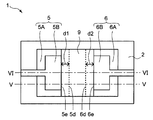
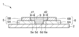
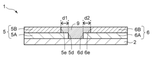
- FIG. 4 shows a modification of the plan view of the active element 1 shown in FIG. 1
- FIG. 5 shows a VV sectional view of the active element 1 in FIG. 4
- FIG. 6 shows the active element 1 in FIG. FIG.
- the upper first electrode 5B may be arranged on the inner side of the lower first electrode 5A.
- the area of the lower first electrode 5A may be larger than the area of the upper first electrode 5B. If at least a part of the upper first electrode 5B is disposed inside the lower first electrode 5A, the contact area between the lower first electrode 5A and the organic semiconductor layer 9 can be increased. Since carriers are efficiently injected into the organic semiconductor layer 9, the operating speed of the active element 1 can be increased.
- At least a part of the upper second electrode 6 ⁇ / b> B is disposed inside the lower second electrode 6 ⁇ / b> A in the surface direction of the substrate 2. May be. Thereby, the area of the lower second electrode 6A may be larger than the area of the upper second electrode 6B.
- the electrode portion of the upper first electrode 5 ⁇ / b> B is preferably disposed on the inner side in the surface direction than the electrode portion of the lower first electrode 5 ⁇ / b> A. Since a part of the lower first electrode 5A is exposed in plan view, the contact area between the lower first electrode 5A and the organic semiconductor layer 9 can be increased as compared with the embodiments of FIGS. it can.
- a part of the wiring portion of the upper first electrode 5B is part of the lower first electrode 5A. It is preferable to be disposed on the electrode part.
- the electrode part of the upper second electrode 6B is arranged on the inner side in the surface direction than the electrode part of the lower second electrode 6A. In this case, it is preferable that a part of the wiring portion of the upper second electrode 6B is disposed on the electrode portion of the lower second electrode 6A.
- the end 5d of the lower first electrode 5A is used.
- the distance d1 from the upper first electrode 5B to the end 5e is preferably 1 nm or more, more preferably 10 nm or more, and further preferably 50 nm or more in the surface direction of the substrate 2.
- the distance d1 from the end 5d of the lower first electrode 5A on the second electrode 6 side to the end 5e of the upper first electrode 5B is preferably 1 nm or more in the surface direction of the substrate 2, and is 10 nm or more. More preferred is 50 nm or more.
- the distance d2 from the end 6d of the lower second electrode 6A to the end 6e of the upper second electrode 6B is preferably 1 nm or more in the surface direction of the substrate 2, and more preferably 10 nm or more. More preferably, it is 50 nm or more.
- the distance d2 from the end 6d of the lower second electrode 6A on the first electrode 5 side to the end 6e of the upper second electrode 6B is preferably 1 nm or more in the surface direction of the substrate 2 and is 10 nm or more. More preferred is 50 nm or more.
- the carrier mobility in the lower first electrode 5A in the plane direction is smaller than the carrier mobility in the upper first electrode 5B.
- the movement time (carrier movement time) required for the carrier to move by the same distance in the lower first electrode 5A or the upper first electrode 5B is lower than the upper first electrode 5B.
- 5A is long, the operation speed of the active element 1 becomes more stable as the difference between the carrier movement time in the lower first electrode 5A and the carrier movement time in the upper first electrode 5B is smaller.
- the distance d1 from the end 5d of the lower first electrode 5A to the end 5e of the upper first electrode 5B is 20 ⁇ m or less in the surface direction of the substrate 2.
- it is 15 ⁇ m or less, more preferably 10 ⁇ m or less.
- the distance d1 from the end 5d of the lower first electrode 5A on the second electrode 6 side to the end 5e of the upper first electrode 5B is preferably 20 ⁇ m or less, more preferably 15 ⁇ m or less in the surface direction of the substrate 2, 10 ⁇ m or less is more preferable.
- the distance d2 from the end 6d of the lower second electrode 6A to the end 6e of the upper second electrode 6B is preferably 20 ⁇ m or less, more preferably 15 ⁇ m or less, and more preferably 10 ⁇ m or less in the surface direction of the substrate 2. Further preferred. In particular, the distance d2 from the end 6d of the lower second electrode 6A on the first electrode 5 side to the end 6e of the upper second electrode 6B is preferably 20 ⁇ m or less, more preferably 15 ⁇ m or less in the surface direction of the substrate 2; 10 ⁇ m or less is more preferable.
- the organic semiconductor layer 9 is (1) the first electrode 5 and the second electrode 6 in the surface direction of the substrate 2. In addition to the region formed between them, (2) in the surface direction of the substrate 2, on the lower first electrode 5A and from the end 5d of the lower first electrode 5A to the end 5e of the upper first electrode 5B. Or (3) in the surface direction of the base material 2, it may be disposed on the lower second electrode 6A and between the end 6d of the lower second electrode 6A and the end 6e of the upper second electrode 6B. . As a result, the contact area between the lower electrode and the organic semiconductor layer 9 increases, so that charge transfer is facilitated.
- the organic semiconductor layer 9 is on the lower first electrode 5A and above the end 5d of the lower first electrode 5A on the second electrode 6 side. It is preferable to arrange between the ends 5e of the first electrode 5B.
- the organic semiconductor layer 9 is on the lower second electrode 6A and on the upper side from the end 6d of the lower second electrode 6A on the first electrode 5 side in the surface direction of the substrate 2. It is preferable that the second electrode 6B is disposed between the ends 6e.
- FIG. 7 shows a modification of the plan view of the active element 1 shown in FIG. 4
- FIG. 8 shows a VIII-VIII sectional view of the active element 1 in FIG. 7
- FIG. 9 shows the active element 1 in FIG. IX-IX cross-sectional view is shown.
- the arrangement of the electrodes shown in FIGS. 7 to 9 is the same as that shown in FIGS.
- the organic semiconductor layer 9 includes (4) the upper first electrode 5B and the upper second electrode 6B in addition to the regions (1), (2) and (3). It may also be formed on the top. Specifically, at least a part of the upper first electrode 5B is arranged between the lower first electrode 5A and the organic semiconductor layer 9 in the thickness direction of the substrate 2, and at least one of the upper second electrode 6B. May be disposed between the lower second electrode 6 ⁇ / b> A and the organic semiconductor layer 9. Thereby, the contact area of the organic semiconductor layer 9 and the lower first electrode 5A and the organic semiconductor layer 9 and the lower second electrode 6A can be increased. In addition, since the contact area between the upper electrode and the organic semiconductor layer 9 is increased and charge is easily exchanged here, the number of carriers contributing to the operation of the active element 1 can be increased, and the operating speed of the active element 1 is increased. Is increased.
- the upper first electrode 5B, the lower first electrode 5A, the upper second electrode 6B, and the lower second electrode 6A have the electrode portion and the wiring portion, respectively, they contribute to the operation of the active element.
- at least a part of the upper first electrode 5B is arranged on the inner side in the plane direction with respect to the lower first electrode 5A, and the organic semiconductor layer 9 Preferably covers the electrode portion of the lower first electrode 5A.
- at least a part of the upper second electrode 6B is disposed on the inner side in the plane direction with respect to the lower second electrode 6A, and the organic semiconductor layer 9 covers the electrode portion of the lower second electrode 6A. preferable.
- FIG. 10 shows a modification of the plan view of the active element 1 shown in FIG. 7, and FIG. 11 shows a XI-XI cross-sectional view of the active element 1 shown in FIG.
- the region of the first electrode 5 opposite to the second electrode 6 and the region of the second electrode 6 opposite to the first electrode 5 are carriers compared to the region between the first electrode 5 and the second electrode 6. Injection is difficult. For this reason, the upper electrode is formed in a region located on the opposite side of the first electrode 5 from the second electrode 6 and in a region located on the opposite side of the second electrode 6 from the first electrode 5 to charge the lower electrode. Collection efficiency may be increased.
- the upper first electrode 5B, the lower first electrode 5A, the upper second electrode 6B, and the lower second electrode 6A have the electrode portion and the wiring portion, respectively.
- at least a part of the electrode portion of the upper first electrode 5B is disposed on the inner side of the electrode portion of the upper first electrode 5B.
- the wiring portion of the first electrode 5B is formed in substantially the same shape as the wiring portion of the lower first electrode 5A. In this case, the end of the lower first electrode 5A opposite to the second electrode 6 and the end of the upper first electrode 5B opposite to the second electrode 6 are arranged to overlap.
- the electrode portion of the upper second electrode 6B is disposed inside the electrode portion of the upper second electrode 6B, and the wiring portion of the upper second electrode 6B is the wiring of the lower second electrode 6A. It is preferable that it is formed in substantially the same shape as the portion. In this case, the end of the lower second electrode 6A opposite to the first electrode 5 and the end of the upper second electrode 6B opposite to the first electrode 5 are arranged to overlap.
- FIGS. 12 shows a modification of the plan view of the active element 1 shown in FIG. 1
- FIG. 13 shows a modification of the plan view of the active element 1 shown in FIG.
- the region sandwiched between the first electrode 5 and the second electrode 6 meander.
- at least a part of the first electrode 5 and at least a part of the second electrode 6 are each formed in a comb shape.
- an electrode arrangement as shown in FIG. Specifically, as shown in FIG. 13, the region sandwiched between the first electrode 5 and the second electrode 6 meanders, and at least the upper first electrode 5 ⁇ / b> B in the surface direction of the substrate 2. It is preferable that a part is disposed inside the lower first electrode 5A and at least a part of the upper second electrode 6B is disposed inside the lower second electrode 6A.
- the active element 1 of the present invention includes an insulating layer 10 formed on the organic semiconductor layer 9 and a third electrode 11 formed on the insulating layer 10. It is preferable.
- the first electrode 5 is a source electrode
- the second electrode 6 is a drain electrode
- the third electrode 11 is a gate electrode
- a top-gate transistor in which the gate electrode is disposed above the source electrode and the drain electrode. Can be configured.
- the active element 1 of the present invention includes a third electrode 11 formed on one main surface of a base 2 and an insulating layer 10 formed on the third electrode 11.
- the first electrode 5, the second electrode 6, and the organic semiconductor layer 9 may be formed on the insulating layer 10.
- the gate electrode is below the source electrode and the drain electrode (side closer to the base material 2).
- a bottom-gate transistor arranged in the above can be formed.
- the insulating layer 10 functions as a gate insulating film.
- the insulating layer 10 is preferably formed from an insulating material such as SiO 2 or SiON.
- the thickness of the insulating layer 10 is preferably 200 nm or more, preferably 250 nm or more, and more preferably 300 nm or more.
- the thickness of the insulating layer 10 is preferably 600 nm or less, more preferably 50 nm or less, and further preferably 500 nm or less.
- the active element 1 of the present invention may have a third electrode 11 formed on the other main surface of the substrate 2.
- the first electrode 5 is a source electrode
- the second electrode 6 is a drain electrode
- the third electrode 11 is a gate electrode
- a transistor in which the substrate 2 also serves as a gate insulating film can be configured.
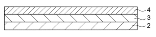
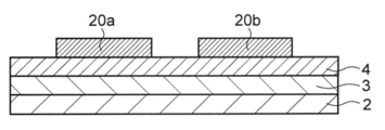
- FIGS. 17 to 24 are sectional views showing a method for manufacturing an active element of the present invention.
- the manufacturing method of the active element of the present invention is as follows: (1) forming a first conductive layer on one main surface of the substrate; (2) forming a second conductive layer on the first conductive layer; (3) forming a mask layer on the second conductive layer; (4) The first conductive layer and the second conductive layer are brought into contact with the etching solution, and the first main surface of the base material is removed by removing a region not covered with the mask layer of the first conductive layer and the second conductive layer.
- a first electrode having a lower first electrode and an upper first electrode on the lower first electrode; and an upper second electrode on the lower second electrode and the lower second electrode.
- the energy barrier between the second conductive layer and the organic semiconductor layer is higher than the energy barrier between the first conductive layer and the organic semiconductor layer, and the conductivity of the second conductive layer is higher than the conductivity of the first conductive layer. It is also characterized by high.
- the active element manufacturing method of the present invention is performed before the step (7) of forming the organic semiconductor layer.
- the steps (5) to (6) the size of the upper first electrode with respect to the lower first electrode and the size of the upper second electrode with respect to the lower second electrode can be reduced. Details of each step will be described.
- Step of forming first conductive layer on one main surface of base material As shown in FIG. 17, the base material 2 is prepared. Although not shown, an adhesion layer, a planarization layer, an optical adjustment layer, and the like may be formed on the main surface of the substrate 2. Moreover, in order to form a terminal electrode and a via electrode in the base material 2, you may form the through-hole (not shown) which penetrates the base material 2 in the thickness direction. For the formation of the through hole, puncturing with a needle-like object, punching, laser processing or the like can be used.
- the first conductive layer 3 is formed on one main surface of the substrate 2.
- the first conductive layer 3 is for forming various electrodes such as a source electrode, a drain electrode, a gate electrode, a terminal electrode, and a via electrode.
- the method for forming the first conductive layer 3 is not particularly limited, and for example, a vacuum deposition method or a sputtering method can be used. Moreover, when the through-hole which penetrates in the thickness direction is not formed in the base material 2, the 1st conductive layer 3 can also be formed into a film by sticking the conductive material formed in foil shape.
- the second conductive layer 4 is formed on the first conductive layer 3. Similar to the first conductive layer 3, the second conductive layer 4 is for forming various electrodes such as a source electrode, a drain electrode, a gate electrode, a terminal electrode, and a via electrode.
- the method for forming the second conductive layer 4 is not particularly limited, and for example, a vacuum deposition method or a sputtering method can be used in the same manner as the formation of the first conductive layer 3. Moreover, when the through-hole which penetrates in the thickness direction is not formed in the base material 2, the 2nd conductive layer 4 can also be formed into a film by sticking the conductive material formed in foil shape.
- the material of the first conductive layer 3 and the second conductive layer 4 can be a conductive material, for example, a metal material such as Cu, Al, Ag, Ni, Au, ITO, ZnO, IGO, IGZO, CuO, etc. Metal materials such as C, carbon nanotubes, graphite, graphene, and other carbon materials can be used.
- the material of the 1st conductive layer 3 is ITO. This is because ITO has a low energy barrier between the organic semiconductor layers 9 and high carrier injection efficiency into the organic semiconductor layer 9.
- the material of the second conductive layer 4 is preferably Cu. Since Cu has a high conductivity, it contributes to an improvement in the operating speed of the active element 1. Further, since Cu is inexpensive, the productivity of the active element 1 can be increased.
- the energy barrier between the second conductive layer 4 and the organic semiconductor layer 9 is higher than the energy barrier between the first conductive layer 3 and the organic semiconductor layer 9, and
- the conductivity of the layer 4 is higher than the conductivity of the first conductive layer 3.
- the first conductive layer 3 forms a lower first electrode 5A and a lower second electrode 6A
- the second conductive layer 4 forms an upper first electrode 5B and an upper second electrode 6B by a step (4) described later.
- the energy barrier between the upper first electrode 5B and the organic semiconductor layer 9 is higher than the energy barrier between the lower first electrode 5A and the organic semiconductor layer 9
- the energy barrier between the upper second electrode 6B and the organic semiconductor layer 9 is higher than the energy barrier between the lower second electrode 6A and the organic semiconductor layer 9.
- the conductivity of the upper first electrode 5B is higher than the conductivity of the lower first electrode 5A
- the conductivity of the upper second electrode 6B is lower than the lower second electrode. It is also higher than the 6A conductivity.
- mask layers 20 a and 20 b are formed on the second conductive layer 4.
- Mask layers 20a and 20b determine the formation positions of first electrode 5 and second electrode 6, respectively.
- a photosensitive resin composition such as a dry film resist or a liquid resist is applied on the second conductive layer 4.
- the photosensitive resin includes a negative type in which the exposed portion is insoluble in the developer and a positive type in which the exposed portion is soluble in the developer.
- a negative photosensitive resin is taken as an example. explain.
- a resist is applied on the second conductive layer 4, and an electron beam or light (ultraviolet rays) is irradiated on the resist to draw a predetermined circuit shape on the resist.
- the shape of the first electrode 5 and the second electrode 6 (for example, a source electrode and a drain electrode in the case of a transistor) is drawn on the resist.
- the circuit shape is transferred and baked on the resist.
- the unexposed portion of each resist is dissolved in the developer.
- the resist exposed portions remain on the second conductive layer 4 as mask layers 20a and 20b.
- the mask layer can be formed of a dry film resist or a liquid resist, but is preferably formed of a dry film resist. Compared with the case where the mask layer is formed of a liquid resist, the solvent drying after applying the resist is unnecessary, so that productivity is improved.
- the first conductive layer and the second conductive layer are brought into contact with the etching solution, and the first main surface of the base material is removed by removing a region not covered with the mask layer of the first conductive layer and the second conductive layer.
- a first electrode having a lower first electrode and an upper first electrode on the lower first electrode; and an upper second electrode on the lower second electrode and the lower second electrode. And forming the second electrode adjacent to the first electrode.
- the first conductive layer 3 and the second conductive layer 4 are brought into contact with the etching solution. By this operation, as shown in FIG. 21, the regions of the first conductive layer 3 and the second conductive layer 4 that are not covered with the mask layer are removed.
- the first electrode 5 having the lower first electrode 5A and the upper first electrode 5B on the lower first electrode 5A, the lower second electrode 6A and the lower electrode on one main surface of the substrate 2
- An upper second electrode 6B on the second side electrode 6A can be formed, and the second electrode 6 disposed adjacent to the first electrode 5 can be formed.
- the lower first electrode 5A, the upper first electrode 5B, the lower second electrode 6A, and the upper second electrode 6B can be formed together, the upper first electrode with respect to the lower first electrode 5A.
- the positional deviation of 5B and the positional deviation of the upper second electrode 6B with respect to the lower second electrode 6A are suppressed.
- an etching solution having a difference between the etching rate for the first conductive layer 3 and the etching rate for the second conductive layer 4 may be used.
- the etching rate of the etching solution with respect to the second conductive layer 4 is higher than the etching rate of the first conductive layer 3.
- a step (5) using another etching solution capable of selectively etching the upper electrode or the lower electrode You may go.
- the mask layer is not peeled off.
- the first electrode 5 and the second electrode 6 may be brought into contact with another etching solution to remove at least a part of the upper first electrode 5B and the upper second electrode 6B.
- another etching solution used here an etching solution that removes the upper first electrode 5B and the upper second electrode 6B without selecting the lower first electrode 5A and the lower second electrode 6A is selected.
- the upper first electrode 5B and the upper second electrode 6B can be side-etched without performing the formation and peeling process of other mask layers, and therefore the upper first electrode in the surface direction of the substrate 2 At least a part of 5B is disposed inside the lower first electrode 5A, and at least a part of the upper second electrode 6B is disposed inside the lower second electrode 6A. Is obtained.
- An organic semiconductor layer 9 is formed so as to cover a region between the first electrode 5 and the second electrode 6.
- the active element 1 in which the organic semiconductor layer 9 is formed on one main surface of the base material 2 from which the first conductive layer 3 and the second conductive layer 4 are removed can be manufactured.
- the step (5) is not performed, an active element 1 as shown in FIGS. 2 to 3 is obtained.
- the active element 1 shown in FIGS. 5 to 6 is obtained. Is obtained.
- the next step (8) can be performed.
- Step of forming an insulating layer on the organic semiconductor layer and forming a third electrode on the insulating layer As shown in FIG. 24, the insulating layer 10 is formed on the organic semiconductor layer 9. Next, as shown in FIG. 14, the third electrode 11 is formed on the insulating layer 10.
- FIG. 14 and FIG. 24 show examples when the step (5) is performed.
- a top gate type transistor in which the first electrode 5, the second electrode 6, and the third electrode 11 correspond to the source electrode, the drain electrode, and the gate electrode, respectively, is manufactured. Can do.
- step (9) can be performed before the step (1).
- Step of forming a third electrode on one main surface of the base material and forming an insulating layer on the third electrode A base material 2 is prepared, and the third electrode 11 is provided on one main surface of the base material 2 Form.
- the third electrode 11 can be formed by a printing method or a photolithography method. When the photolithography method is used, a mask layer having a desired shape is formed on the third conductive layer after forming a third conductive layer (not shown) in the same manner as the formation of the first electrode 5 and the second electrode 6. Then, the third electrode 11 is formed by bringing the third conductive layer into contact with the etching solution.
- the insulating layer 10 is formed on the third electrode 11.
- the first electrode 5, the second electrode 6, and the third electrode 11 are transistors on the bottom gate side corresponding to the source electrode, the drain electrode, and the gate electrode, respectively. Can be manufactured.
- FIG. 15 shows an example when the step (5) is performed.
- FIG. 25 illustrates a cross-sectional view of the active element 1 according to the first embodiment.
- FIG. 25 shows a configuration example in which the insulating layer 10 and the third electrode 11 are formed on the organic semiconductor layer 9 of the semiconductor element shown in FIG.
- at least a part of the upper first electrode 5B is formed inside the lower first electrode 5A, and at least a part of the upper second electrode 6B is located inside the lower second electrode 6A.
- the formed top gate transistor was manufactured as Sample 1. Specifically, a source electrode (first electrode) and a drain electrode (second electrode) having a channel length of 53 ⁇ m and a channel width of 483 ⁇ m are formed on one main surface of a polyethylene naphthalate (PEN) film as the substrate 2.
- PEN polyethylene naphthalate
- DNTT was formed by vacuum deposition on the region between the first electrode 5 and the second electrode 6 and on the first electrode 5 and the second electrode 6 to form the organic semiconductor layer 9.
- the distance from the end of the lower first electrode 5 ⁇ / b> A on the second electrode 6 side to the end of the upper first electrode 5 ⁇ / b> B is 2 ⁇ m in the surface direction of the substrate 2
- the distance from the end of the second side electrode 6 ⁇ / b> A to the end of the upper second electrode 6 ⁇ / b> B was 2 ⁇ m in the surface direction of the substrate 2.
- An insulating layer 10 was formed on the organic semiconductor layer 9, and a gate electrode (third electrode 11) was further formed on the insulating layer 10. Cu was used as the material of the third electrode 11.
- FIG. 26 is a sectional view of the active element 1 according to the second embodiment.
- sample 2 was fabricated in which upper first electrode 5B and lower first electrode 5A have substantially the same shape, and upper second electrode 6B and lower second electrode 6A have substantially the same shape.
- DNTT was formed on the region between the first electrode 5 and the second electrode 6 and on the first electrode 5 and the second electrode 6 to form the organic semiconductor layer 9. Conditions other than those described above were the same as those for sample 1.
- FIG. 27 is a cross-sectional view of the active element 100 according to the first comparative example.
- a top-gate transistor having a single-layer structure of the first electrode 51 and the second electrode 52 was manufactured as a sample 3.
- the first electrode 51 (source electrode) and the second electrode 52 (drain electrode) were each formed in a single layer structure on the PEN as the substrate 50.
- DNTT was formed on the region between the first electrode 51 and the second electrode 52, and on the first electrode 51 and the second electrode 52, thereby forming the organic semiconductor layer 54.
- an insulating layer 55 was formed on the organic semiconductor layer 54, and a third electrode 53 (gate electrode) was formed on the insulating layer 55.
- the electrode material of the first electrode 51 and the second electrode 52 was ITO
- the electrode material of the third electrode 53 was Cu, and other conditions were the same as those of the sample 1.
- FIG. 28 is a cross-sectional view of the active element 100 according to Comparative Examples 2 to 3.
- the third electrode 53 gate electrode
- the insulating layer 55 was formed on the third electrode 53.
- the first electrode 51 source electrode
- the second electrode 52 drain electrode
- DNTT is formed on the region between the first electrode 51 and the second electrode 52 and on the first electrode 51 and the second electrode 52 to form an organic semiconductor layer 54.
- Sample 4 was prepared. The channel length was 65 ⁇ m, the channel width was 349 ⁇ m, and the electrode material was Cu.
- Sample 5 was prepared in the same manner as Sample 4 except that the electrode material of the first electrode and the second electrode was Au.
- the gate voltage-drain current characteristics were measured with a 4200-SCS type semiconductor parameter analyzer manufactured by KEITHLEY.
- the measurement conditions of the transfer characteristics were a drain voltage of ⁇ 20V and a gate voltage of 5V to ⁇ 20V.
- the mobility was calculated from the obtained transfer characteristics.
- Table 1 shows the types of the first electrode and the second electrode, the channel length ( ⁇ m), the channel width ( ⁇ m), the mobility (cm 2 / V ⁇ sec), and the maximum drain current (A) of each sample.
- FIG. 29 shows a gate voltage-drain current characteristic (transfer characteristic) when a drain voltage of ⁇ 20V is applied and the gate voltage is changed from 5V to ⁇ 20V.
- the vertical axis represents the absolute value (A) of the drain current
- the horizontal axis represents the gate voltage (V). Since DNTT used this time is a p-type semiconductor, the absolute value of the drain current flowing when the gate voltage is negative is large.
- the transfer characteristic in the negative voltage region of sample 1 was inferior to that of sample 3 (ITO) but exceeded that of sample 4 (Cu) depending on the gate voltage value.
- the upper electrode It has been found that it is preferable to provide a step by disposing at least a part of the inner side of the lower electrode.
- Active element 2 Base material 3: First conductive layer 4: Second conductive layer 5: First electrode 5A: Lower first electrode 5B: Upper first electrode 6: Second electrode 6A: Lower second electrode 6B: Upper second electrode 9: Organic semiconductor layer 10: Insulating layer 11: Third electrode 20a, 20b: Mask layer
Landscapes
- Thin Film Transistor (AREA)
- Electroluminescent Light Sources (AREA)
- Electrodes Of Semiconductors (AREA)
Abstract
【課題】本発明は、材料費を抑えつつ必要な動作速度を確保することができる能動素子と、その製造方法を提供する。 【解決手段】本発明の能動素子1は;基材2と;基材2の一方主面上の第1電極5と;第1電極5と隣り合って配置されている第2電極6と;基材2の一方主面上であって、少なくとも第1電極5と第2電極6の間の領域を覆うように形成されている有機半導体層9と、を有し;上側第1電極5Bと有機半導体層9の間のエネルギー障壁が、下側第1電極5Aと有機半導体層9の間のエネルギー障壁よりも高く;上側第2電極6Bと有機半導体層9の間のエネルギー障壁が、下側第2電極6Aと有機半導体層9の間のエネルギー障壁よりも高く;上側第1電極5Bの導電率が、下側第1電極5Aの導電率よりも高く;上側第2電極6Bの導電率が、下側第2電極6Aの導電率よりも高いものである。
Description
本発明は、半導体層に有機半導体を用いた能動素子に関するものである。
近年、能動素子の薄型化、フレキシブル化、軽量化、大面積化等の要望が高まるにつれて、基材材料としてはポリエチレンナフタレート(PEN)やポリイミド(PI)等の高分子フィルムが使用されている。これに伴い、半導体層として、当該フィルムの耐熱温度以下で成膜が可能な有機半導体を用いた能動素子が種々開発されている。有機半導体を用いた能動素子の電極材料は、有機半導体との間のエネルギー障壁が小さく、導電率の高いAuが使用されている(例えば、非特許文献1を参照)。
岩佐義宏、竹延大志、"有機トランジスタ"、[online]、2008年、応用物理学会、[2015年9月3日検索]、インターネット<URL:http://www.jsap.or.jp/editorial/KISO-sample/QOBU0414.pdf>
能動素子の電極材料へのAuの使用は、能動素子の性能の向上には寄与するものの、材料費の増大が懸念されるため、安価に能動素子を製造したい場合に障害になるおそれがある。
そこで、本発明は、材料費を抑えつつ必要な動作速度を確保することができる能動素子と、その製造方法を提供することを目的とする。
本発明者は、Auの代替となる電極材料について検討した。電極材料としては、導電率が高く安価に得られるCuが工業生産上適しているが、Cuは有機半導体との間のエネルギー障壁が比較的高いため高いキャリア注入効率を得るためには課題がある。そこで本発明者は、材料費を抑えながらもAu並みの性能を有する電極材料を検討する中で、電極を複数の材料を組み合わせて積層構造とすることに想到した。そして、この上下2層の積層構造を有する電極において、有機半導体層と接触しやすい下側電極には高いキャリア注入効率を有する材料を、下側電極よりも有機半導体層と接触しにくい上側電極には高い導電性を有する材料を用いることを見出した。
上記目的を達成し得た本発明の能動素子は;基材と;基材の一方主面上に形成されている下側第1電極と、下側第1電極上に形成されている上側第1電極と、を含む第1電極と;基材の一方主面上に形成されている下側第2電極と、下側第2電極上に形成されている上側第2電極と、を含み、第1電極と隣り合って配置されている第2電極と;基材の一方主面上であって、少なくとも第1電極と第2電極の間の領域を覆うように形成されている有機半導体層と、を有し;上側第1電極と有機半導体層の間のエネルギー障壁が、下側第1電極と有機半導体層の間のエネルギー障壁よりも高く;上側第2電極と有機半導体層の間のエネルギー障壁が、下側第2電極と有機半導体層の間のエネルギー障壁よりも高く;上側第1電極の導電率が、下側第1電極の導電率よりも高く;上側第2電極の導電率が、下側第2電極の導電率よりも高いことを特徴とする。電極と有機半導体層の間のエネルギー障壁はキャリア注入効率に影響するため、本発明の能動素子は、上側第1電極-有機半導体層のキャリア注入効率よりも下側第1電極-有機半導体層のキャリア注入効率が高く、上側第2電極-有機半導体層のキャリア注入効率よりも下側第2電極-有機半導体層のキャリア注入効率が高いものである。このため、下側に配置される下側第1電極、下側第2電極では有機半導体層との電荷の授受がなされやすい。一方、本発明の能動素子は、上側第1電極の導電率が下側第1電極の導電率よりも高く、上側第2電極の導電率が下側第2電極の導電率よりも高いものである。このため、上側に配置される上側第1電極、上側第2電極では、下側に配置される電極から、或いは下側に配置される電極へ電気伝導がなされやすくなるため、動作速度を高められる。このように、本発明の能動素子は第1電極と第2電極が積層構造であり、上側と下側で電極材料および形状を独立して設計できるため、良好な動作特性と安価な材料の選択可能性を両立できるものである。
基材の面方向において、上側第1電極の少なくとも一部が、下側第1電極よりも内側に配置されており、基材の面方向において、上側第2電極の少なくとも一部が、下側第2電極よりも内側に配置されていることが好ましい。上側第1電極の少なくとも一部が、下側第1電極より内側に配置されていれば、下側第1電極と有機半導体層との接触面積を増加させることができ、電極から有機半導体層には効率的にキャリアが注入されるため、能動素子の動作速度を高められる。下側第2電極と上側第2電極についても同様である。
下側第1電極の端から上側第1電極の端までの距離が、基材の面方向において1nm以上20μm以下であり、下側第2電極の端から上側第2電極の端までの距離が、基材の面方向において1nm以上20μm以下であることが好ましい。上記のとおり下限を設定することにより、下側第1電極と有機半導体層、或いは下側第2電極と有機半導体層の接触面積が増えるため、キャリア注入効率を高めることができる。また、上記のとおり上限を設定することにより、能動素子を安定して動作させることができる。
基材の面方向において、有機半導体層が、下側第1電極上であって下側第1電極の端から上側第1電極の端の間と、下側第2電極上であって下側第2電極の端から上側第2電極の端の間に配置されていることが好ましい。これにより、下側第1電極と有機半導体層、および下側第2電極と有機半導体層との接触面積が増加するため、電荷の授受がなされやすくなる。
基材の厚み方向において、上側第1電極の少なくとも一部が下側第1電極と有機半導体層の間に配置されており、上側第2電極の少なくとも一部が下側第2電極と有機半導体層の間に配置されていることが好ましい。これにより、有機半導体層と下側第1電極、および有機半導体層と下側第2電極との接触面積を増加させることができる。また、上側電極と有機半導体層の接触面積も増加し、ここでも電荷の授受がなされやすくなるため、能動素子の動作に寄与するキャリア数を増加することができ、能動素子の動作速度が高められ
る。
る。
上側第1電極、下側第1電極、上側第2電極、下側第2電極は、電極部と、電極部よりも幅狭に形成されている配線部と、をそれぞれ有しており、基材の面方向において、上側第1電極の電極部は、下側第1電極の電極部よりも内側に配置されており、基材の面方向において、上側第2電極の電極部は、下側第2電極の電極部よりも内側に配置されていることが好ましい。下側第1電極と有機半導体層、或いは下側第2電極と有機半導体層の接触面積を増加させることができる。
第1電極と第2電極に挟まれている領域が蛇行していることが好ましい。これにより、第1電極と有機半導体層、或いは第2電極と有機半導体層の接触長さが増加するため、第1電極と第2電極の間に流れる電流を大きくすることができる。
下側第1電極および下側第2電極の材料がITOであり、上側第1電極および上側第2電極の材料がCuであることが好ましい。ITOは、有機半導体層との間のエネルギー障壁が低く、有機半導体層へのキャリア注入効率が高いからである。Cuは導電率が高いため、能動素子の動作速度の向上に寄与する。また、Cuは安価であるから、能動素子の生産性を高めることができる。
有機半導体層上に形成されている絶縁層と、絶縁層上に形成されている第3電極と、を有することが好ましい。これにより、トップゲート型のトランジスタを構成することができる。
基材の一方主面上に形成されている第3電極と、第3電極上に形成されている絶縁層と、を有し、第1電極、第2電極、有機半導体層が、絶縁層上に形成されていることが好ましい。これにより、ボトムゲート型のトランジスタを構成することができる。
基材の他方主面上に形成されている第3電極を有することが好ましい。これにより、基材がゲート絶縁膜を兼ねているトランジスタを構成することができる。
上記目的を達成し得た本発明の能動素子の製造方法は;基材の一方主面上に第1導電層を形成する工程と;第1導電層上に第2導電層を形成する工程と;第2導電層上にマスク層を形成する工程と;第1導電層および第2導電層をエッチング液に接触させて、第1導電層および第2導電層のマスク層で覆われていない領域を除去することにより、基材の一方主面上に、下側第1電極と下側第1電極上の上側第1電極とを有する第1電極と、下側第2電極と下側第2電極上の上側第2電極とを有しており、第1電極と隣り合って配置されている第2電極と、を形成する工程と;基材の一方主面上であって、少なくとも第1電極と第2電極の間の領域を覆うように有機半導体層を形成する工程と、を含み;第2導電層と有機半導体層の間のエネルギー障壁が、第1導電層と有機半導体層の間のエネルギー障壁よりも高く;第2導電層の導電率が、第1導電層の導電率よりも高いことを特徴とする。本発明では、下側第1電極、上側第1電極、下側第2電極、上側第2電極を一緒に形成することができるため、下側第1電極に対する上側第1電極の位置ズレや、下側第2電極に対する上側第2電極の位置ズレが抑制される。
有機半導体層を形成する前に、第1電極および第2電極を他のエッチング液に接触させて、上側第1電極および上側第2電極の少なくとも一部領域を除去する工程を含むことが好ましい。これにより、他のマスク層の形成および剥離工程を実施することなく、上側第1電極および上側第2電極をサイドエッチングすることができるため、基材の面方向において、上側第1電極の少なくとも一部が、下側第1電極よりも内側に配置されており、上側第2電極の少なくとも一部が、下側第2電極よりも内側に配置されている能動素子1が得られる。
本発明の能動素子は、下側第1電極および下側第2電極のキャリア注入効率が高いため有機半導体層との電荷の授受がなされやすく、上側第1電極および上側第2電極では、下側に配置される電極から、或いは下側に配置される電極への電気伝導がなされやすいため動作速度を高められる。このように、上側と下側で電極材料および形状を独立して設計できる積層構造とすることにより、良好な動作特性と安価な材料の選択可能性を両立できる。
また、本発明の能動素子の製造方法では、下側第1電極、上側第1電極、下側第2電極、上側第2電極を一緒に形成することができるため、下側第1電極に対する上側第1電極の位置ズレや、下側第2電極に対する上側第2電極の位置ズレが抑制される。
また、本発明の能動素子の製造方法では、下側第1電極、上側第1電極、下側第2電極、上側第2電極を一緒に形成することができるため、下側第1電極に対する上側第1電極の位置ズレや、下側第2電極に対する上側第2電極の位置ズレが抑制される。
以下、実施の形態に基づき本発明をより具体的に説明するが、本発明はもとより下記実施の形態によって制限を受けるものではなく、前・後記の趣旨に適合し得る範囲で変更を加えて実施することも勿論可能であり、それらはいずれも本発明の技術的範囲に包含される。また、図面における種々部材の寸法比は、本発明の特徴の理解に資することを優先しているため、実際の寸法比とは異なる場合がある。
1.能動素子
本発明において能動素子は、信号増幅や整流を行う素子であり、例えばトランジスタ、サイリスタ、ダイオード等の半導体素子である。これらの応用例としては、例えば、ディスプレイ、タッチパネル、太陽電池、半導体レーザー、圧力センサー、生体センサー等がある。
本発明において能動素子は、信号増幅や整流を行う素子であり、例えばトランジスタ、サイリスタ、ダイオード等の半導体素子である。これらの応用例としては、例えば、ディスプレイ、タッチパネル、太陽電池、半導体レーザー、圧力センサー、生体センサー等がある。
本発明において能動素子は、厚み方向と面方向を有する。能動素子の厚み方向は、基材、第1電極、第2電極、有機半導体層が積層される方向であり、能動素子の面方向は、厚み方向と直交する方向である。
図1は、本発明の能動素子の平面図を表し、図2は、図1に示した能動素子のII-II断面図を表し、図3は、図1に示した能動素子のIII-III断面図を表す。図1~図3に示すように、本発明の能動素子1は、基材2と、下側第1電極5Aと上側第1電極5Bを含む第1電極5と、下側第2電極6Aと上側第2電極6Bを含む第2電極6と、有機半導体層9と、を有する。
基材2は、一方主面と他方主面を有しており、第1電極5、第2電極6、有機半導体層9を支持するために設けられる。
基材2は、例えば、ポリエチレンナフタレート(PEN)、ポリエチレンテレフタレート(PET)、ポリイミド(PI)等の高分子フィルムからなるフレキシブル基板や、ガラス基板等のリジッド基板が好ましく用いられる。
基材2の折れや破れを防止するために、基材2の厚みは、例えば5μm以上であることが好ましく、10μm以上であることがより好ましく、18μm以上であることがさらに好ましい。他方、能動素子1の薄型化の観点からは、基材2の厚みは、200μm以下であることが好ましく、150μm以下であることが好ましく、125μm以下であることがさらに好ましい。
後述するように、基材2が絶縁層10を兼ねるフィルムの場合には、基材2の厚みは、10μm以下であることが好ましく、7μm以下であることがより好ましく、5μm以下であることがさらに好ましく、0.1μm以上であることが好ましく、0.5μm以上であることがより好ましく、1μm以上であることがさらに好ましい。
図2~図3に示すように、有機半導体層9は、基材2の一方主面上であって、少なくとも第1電極5と第2電極6の間の領域を覆うように形成されている。有機半導体層9は、トランジスタの場合にはチャネル領域として機能する。有機半導体層9の材料としては、例えば、ペンタセン、アントラセン、テトラセン、ルブレン、ジナフトチエノチオフェン、ポリアセチレン、ポリチオフェン、フラーレン、カーボンナノチューブ等を用いることができる。
有機半導体層9の厚みの上限は特に制限されないが、薄型の能動素子1を得るためには、有機半導体層9の厚みは、例えば、200nm以下であることが好ましく、150nm以下であることがより好ましく、100nm以下であることがさらに好ましい。
有機半導体層9は、真空蒸着法や印刷法によって好ましく形成される。詳細には、印刷法では、有機半導体の分子を塗布用の有機溶媒に分散させた混合液体(以下、「有機半導体インキ」と称する)を、基材2に塗布した後、乾燥させることにより形成される。
印刷法によって有機半導体層9が形成される場合、有機溶媒としては、例えばメシチレン、トルエン、クロロホルム、p-ジイソプロピルベンゼン、ベンジルアルコールやこれらの混合溶媒を用いることができる。
図1~図3に示すように、本発明の能動素子1は、基材2の一方主面上に隣り合って形成されている第1電極5および第2電極6とを有する。
第1電極5、第2電極6、後述する第3電極(以下、まとめて「電極」と称することもある)は能動素子1を動作させるために電気的に接続されるものであり、例えば、能動素子1がトランジスタの場合には、第1電極5はソース電極に相当し、第2電極6はドレイン電極に相当し、第3電極11はゲート電極に相当する。
電極の材料は導電性材料を用いることができ、例えば、Cu、Al、Ag、Ni、Au等の金属材料、ITO、ZnO、IGO、IGZO、CuO等の金属酸化物、C、カーボンナノチューブ、グラファイト、グラフェン等の炭素材料等を用いることができる。
電極は、例えば、フォトリソグラフィ法や印刷法によって形成することができる。第1電極5と第2電極6の相対位置の精度を向上させる観点からは、第1電極5および第2電極6は、フォトリソグラフィ法によって形成されることが好ましい。
電極の厚みは、必要な導電率を確保するために、例えば、5nm以上であることが好ましく、10nm以上であることがより好ましく、20nm以上であることがさらに好ましい。電極の厚みの上限は特に制限されないが、能動素子1全体の厚みが増加するのを抑制し、フォトリソグラフィ法を用いる場合にエッチング時間を短縮する観点から、例えば、1μm以下であることが好ましく、700nm以下であることがより好ましく、500nm以下であることがさらに好ましい。
第1電極5と第2電極6は隣り合って形成されていればよく、第1電極5の一つの辺と第2電極6の一つの辺が対向して配置されていてもよい。例えば、図1では、第1電極5の一辺5Cと、第2電極6の一辺6Cが対向するように配置されている。
図1~図3に示すように、第1電極5は、基材2の一方主面上に形成されている下側第1電極5Aと、下側第1電極5A上に形成されている上側第1電極5Bとを有している。第1電極5と同様に、第2電極6は、基材2の一方主面上に形成されている下側第2電極6Aと、下側第2電極6A上に形成されている上側第2電極6Bとを有している。
本発明の能動素子1は第1電極5と第2電極6が積層構造であり、上側と下側で電極材料および形状を独立して設計できるため、良好な動作特性と安価な材料の選択可能性を両立できるものである。積層構造の電極では、下側に配置される下側第1電極5Aや下側第2電極6A(以下、まとめて「下側電極」と称することもある)は、上側に配置される上側第1電極5Bや上側第2電極6B(以下、まとめて「上側電極」と称することもある)に比べて有機半導体層9との接触面積が大きくなりやすい。このため、主に下側電極では、電極から有機半導体層9或いは有機半導体層9から電極に電荷キャリア(以下単に「キャリア」と称する)の注入がなされる。これに対して、上側電極は主に下側電極、或いは外部配線(図示せず)との間で電荷の授受を行う役割を有する。
積層構造をなすために、上側電極と下側電極は異なる材料から形成される。また、後述する「2.能動素子の製造方法」のとおり、第1導電層から下側第1電極5Aおよび下側第2電極6Aを形成し、第2導電層から上側第1電極5Bおよび上側第2電極6Bを形成することによって、下側第1電極5Aと下側第2電極6Aが同じ材料から形成され、上側第1電極5Bと上側第2電極6Bが同じ材料から形成されてもよい。
下側電極としては、キャリア注入効率が高い材料、例えば、ITO、IGZO、ZnO、IGO、CuOが用いられることが好ましく、ITOが用いられることがより好ましい。
上側電極としては、能動素子1の動作速度を高めるために、導電率やキャリア移動度が高い材料、例えば、Cu、Alが用いられることが好ましく、Cuが用いられることがより好ましい。
電極-有機半導体層9の間のエネルギー障壁の値が低いほど、有機半導体層9から電極、或いは電極から有機半導体層9に注入されるキャリアの割合であるキャリア注入効率は増加し、能動素子の動作速度が向上すると考えられている。したがって、本発明の能動素子1は、上側第1電極5Bと有機半導体層9の間のエネルギー障壁が、下側第1電極5Aと有機半導体層9の間のエネルギー障壁よりも高く、上側第2電極6Bと有機半導体層9の間のエネルギー障壁が、下側第2電極6Aと有機半導体層9の間のエネルギー障壁よりも高いものである。
本発明において、電極と有機半導体層9の間のエネルギー障壁(単位:eV)は、電極の仕事関数Φe(単位:eV)と有機半導体層9の仕事関数Φos(単位:eV)の差の絶対値|Φe-Φos|から求める。
仕事関数の測定には、主に、光電子効果を利用した方法と、2種類の導体の接触電位差を用いた方法があるが、本発明では前者の方法を利用した理研計器製の大気中光電子分光装置(型番:AC-3)を用いる。
上側電極と有機半導体層9の間のエネルギー障壁と、下側電極と有機半導体層9の間のエネルギー障壁の具体的な値は、例えば以下のように設定される。
上側第1電極5Bと有機半導体層9の間のエネルギー障壁は、下側第1電極5Aと有機半導体層9の間のエネルギー障壁の1.1倍以上であることが好ましく、1.3倍以上であることがより好ましく、1.5倍以上であることがさらに好ましい。
同様に上側第2電極6Bと有機半導体層9の間のエネルギー障壁は、下側第2電極6Aと有機半導体層9の間のエネルギー障壁の1.1倍以上であることが好ましく、1.3倍以上であることがより好ましく、1.5倍以上であることがさらに好ましい。
他方、上側電極は、下側電極或いは外部配線の間で電荷の授受を行う役割を有しているため導電率が高いほどよい。したがって、本発明の能動素子1は、上側第1電極5Bの導電率が、下側第1電極5Aの導電率よりも高く、上側第2電極6Bの導電率が、下側第2電極6Aの導電率よりも高いものである。
本発明において導電率(単位:S/m)の測定は、JIS H 0505:1975 非鉄金属材料の体積抵抗率及び導電率測定方法に基づき行うものとする。
上側電極と下側電極の導電率の具体的な値は、例えば以下のように設定される。
上側第1電極5Bの導電率が、下側第1電極5Aの導電率の100倍以上であることが好ましく、1000倍以上であることがより好ましく、10000倍以上であることがさらに好ましい。
同様に、上側第2電極6Bの導電率が、下側第2電極6Aの導電率の100倍以上であることが好ましく、1000倍以上であることがより好ましく、10000倍以上であることがさらに好ましい。
上側第1電極5B、下側第1電極5A、上側第2電極6B、下側第2電極6Aは、多角形状(好ましくは四角形状)の電極部と、電極部よりも幅狭に形成されている配線部と、をそれぞれ有していてもよい。下側電極の電極部は、主に有機半導体層9と接触して上側電極を支持し、下側電極の配線部は主に上側電極を支持する。上側電極の電極部は、主に下側電極との電荷の授受を行うものであり、上側電極の配線部は、主に上側電極の電極部と外部配線とを接続する役割を有する。能動素子がトランジスタの場合には、チャネル領域の面積を大きくするために、第1電極5の電極部と第2電極6の電極部が隣り合って形成されることが好ましい。
基材2の面方向において、上側電極と下側電極の大小関係は特に制限されないが、製造工程を簡略化するために、図1~図3に示すように、下側第1電極5Aと上側第1電極5Bが略同形状に形成されていてもよい。第1電極5と同様に、製造工程を簡略化するために、下側第2電極6Aと上側第2電極6Bが略同形状に形成されていてもよい。
上側第1電極5B、下側第1電極5A、上側第2電極6B、下側第2電極6Aが、それぞれ上記電極部と上記配線部を有している場合には、下側第1電極5Aの電極部の端が上側第1電極5Bの電極部の端と重なって配置されており、下側第2電極6Aの電極部の端が上側第2電極6Bの電極部の端と重なって配置されることが好ましい。
第1電極5と第2電極6の配置間隔は特に制限されないが、例えば第1電極5がソース電極で、第2電極6がドレイン電極であるトランジスタの場合には、第1電極5と第2電極6の間の長さであるチャネル長は20μm以下であることが好ましく、15μm以下であることがより好ましく、10μm以下であることがさらに好ましい。チャネル長が短いほど、トランジスタの処理速度と集積度を高めることができる。
次に、基材2の面方向において、上側電極と下側電極の大きさが異なり、電極が階段状に形成されている構成例について説明する。例えば、上側第1電極5Bの少なくとも一部が、下側第1電極5Aよりも外側に配置されてもよい(図示せず)。これにより、上側第1電極5Bの面積は、下側第1電極5Aの面積より大きくてもよい(図示せず)。上側第1電極5Bの材料として、導電率や移動度が高い材料を採用することにより、能動素子1の動作速度を高められる。同様の理由から、上側第2電極6Bの面積は、下側第2電極6Aの面積より大きくてもよい(図示せず)。
図4は、図1に示した能動素子1の平面図の変形例を表し、図5は、図4の能動素子1のV-V断面図を表し、図6は、図4の能動素子1のVI-VI断面図を表す。図4~図6に示すように、基材2の面方向において、上側第1電極5Bの少なくとも一部が、下側第1電極5Aより内側に配置されてもよい。これにより、下側第1電極5Aの面積が上側第1電極5Bの面積より大きくてもよい。上側第1電極5Bの少なくとも一部が、下側第1電極5Aより内側に配置されていれば、下側第1電極5Aと有機半導体層9との接触面積を増加させることができ、電極から有機半導体層9には効率的にキャリアが注入されるため、能動素子1の動作速度を高められる。第1電極5と同様の理由から、図4~図6に示すように、基材2の面方向において、上側第2電極6Bの少なくとも一部が、下側第2電極6Aより内側に配置されてもよい。これにより、下側第2電極6Aの面積が上側第2電極6Bの面積より大きくてもよい。
上側第1電極5B、下側第1電極5A、上側第2電極6B、下側第2電極6Aが、それぞれ上記電極部と上記配線部を有している場合には、図4~図6に示すように、基材2の面方向において、上側第1電極5Bの電極部が、下側第1電極5Aの電極部よりも面方向内側に配置されていることが好ましい。平面視で下側第1電極5Aの一部が露出しているため、図1~図3の態様と比較して下側第1電極5Aと有機半導体層9との接触面積を増加させることができる。なお、上側第1電極5Bの電極部を下側第1電極5Aの電極部よりも面方向内側に配置するために、上側第1電極5Bの配線部の一部は下側第1電極5Aの電極部の上に配置されていることが好ましい。同様の理由から、基材2の面方向において、上側第2電極6Bの電極部が、下側第2電極6Aの電極部よりも面方向内側に配置されていることが好ましい。この場合、上側第2電極6Bの配線部の一部は下側第2電極6Aの電極部の上に配置されていることが好ましい。
図4~図6に示す能動素子1において、下側第1電極5Aと有機半導体層9との接触面積を増やして電荷の授受がなされやすくなるためには、下側第1電極5Aの端5dから上側第1電極5Bの端5eまでの距離d1は、基材2の面方向において1nm以上であることが好ましく、10nm以上がより好ましく、50nm以上がさらに好ましい。特に、第2電極6側の下側第1電極5Aの端5dから上側第1電極5Bの端5eまでの距離d1は、基材2の面方向において1nm以上であることが好ましく、10nm以上がより好ましく、50nm以上がさらに好ましい。同様の理由から、下側第2電極6Aの端6dから上側第2電極6Bの端6eまでの距離d2は、基材2の面方向において1nm以上であることが好ましく、10nm以上がより好ましく、50nm以上がさらに好ましい。特に、第1電極5側の下側第2電極6Aの端6dから上側第2電極6Bの端6eまでの距離d2は、基材2の面方向において1nm以上であることが好ましく、10nm以上がより好ましく、50nm以上がさらに好ましい。
下側第1電極5Aは上側第1電極5Bよりも導電率が低いため、面方向における下側第1電極5A中のキャリア移動度は、上側第1電極5B中のキャリア移動度よりも小さい。このため、キャリアが下側第1電極5A内、或いは上側第1電極5B内を同じ距離だけ移動するのに要する移動時間(キャリア移動時間)は、上側第1電極5Bよりも下側第1電極5Aが長いが、下側第1電極5A内でのキャリア移動時間と上側第1電極5B内でのキャリア移動時間の差は小さいほど能動素子1の動作速度が安定する。このため、能動素子1を安定して動作させる観点からは、下側第1電極5Aの端5dから上側第1電極5Bの端5eまでの距離d1は、基材2の面方向において20μm以下が好ましく、15μm以下がより好ましく、10μm以下がさらに好ましい。特に、第2電極6側の下側第1電極5Aの端5dから上側第1電極5Bの端5eまでの距離d1は、基材2の面方向において20μm以下が好ましく、15μm以下がより好ましく、10μm以下がさらに好ましい。同様の理由から、下側第2電極6Aの端6dから上側第2電極6Bの端6eまでの距離d2は、基材2の面方向において20μm以下が好ましく、15μm以下がより好ましく、10μm以下がさらに好ましい。特に、第1電極5側の下側第2電極6Aの端6dから上側第2電極6Bの端6eまでの距離d2は、基材2の面方向において20μm以下が好ましく、15μm以下がより好ましく、10μm以下がさらに好ましい。
図4~図6に示すように第1電極5、第2電極6が配置される場合、有機半導体層9は(1)基材2の面方向において、第1電極5と第2電極6の間に形成されている領域のほか、(2)基材2の面方向において、下側第1電極5A上であって下側第1電極5Aの端5dから上側第1電極5Bの端5eの間や、(3)基材2の面方向において、下側第2電極6A上であって下側第2電極6Aの端6dから上側第2電極6Bの端6eの間に配置されてもよい。これにより、下側電極と有機半導体層9との接触面積が増加するため、電荷の授受がなされやすくなる。特に、(2)の領域について、有機半導体層9は、基材2の面方向において、下側第1電極5A上であって第2電極6側の下側第1電極5Aの端5dから上側第1電極5Bの端5eの間に配置されることが好ましい。また、(3)の領域について、有機半導体層9は、基材2の面方向において、下側第2電極6A上であって第1電極5側の下側第2電極6Aの端6dから上側第2電極6Bの端6eの間に配置されることが好ましい。
図7~図9を用いて、有機半導体層9の別の配置例について説明する。図7は、図4に示した能動素子1の平面図の変形例を表し、図8は、図7の能動素子1のVIII-VIII断面図を表し、図9は、図7の能動素子1のIX-IX断面図を表す。なお、図7~図9に示す電極の配置は、図4~図6の配置と同じである。
図7~図9に示すように、有機半導体層9は、上記(1)、(2)、(3)の領域に加えて、(4)上側第1電極5Bの上および上側第2電極6Bの上にも形成されてもよい。詳細には、基材2の厚み方向において、上側第1電極5Bの少なくとも一部が、下側第1電極5Aと有機半導体層9の間に配置されており、上側第2電極6Bの少なくとも一部が、下側第2電極6Aと有機半導体層9の間に配置されていてもよい。これにより、有機半導体層9と下側第1電極5A、および有機半導体層9と下側第2電極6Aとの接触面積を増加させることができる。また、上側電極と有機半導体層9の接触面積も増加し、ここでも電荷の授受がなされやすくなるため、能動素子1の動作に寄与するキャリア数を増加することができ、能動素子1の動作速度が高められる。
上側第1電極5B、下側第1電極5A、上側第2電極6B、下側第2電極6Aが、それぞれ上記電極部と上記配線部を有している場合には、能動素子の動作に寄与するキャリア数を増加するために、図7~図9に示すように、上側第1電極5Bの少なくとも一部が下側第1電極5Aよりも面方向内側に配置されており、有機半導体層9が下側第1電極5Aの電極部を覆っていることが好ましい。同様に、上側第2電極6Bの少なくとも一部が下側第2電極6Aよりも面方向内側に配置されており、有機半導体層9が下側第2電極6Aの電極部を覆っていることが好ましい。
図10~図11を用いて、第1電極5および第2電極6の他の構成例について説明する。図10は、図7に示した能動素子1の平面図の変形例を表し、図11は図10の能動素子1のXI-XI断面図を表す。第1電極5の第2電極6とは反対側の領域および第2電極6の第1電極5とは反対側の領域は、第1電極5と第2電極6の間の領域と比べてキャリア注入がなされにくい。このため、第1電極5の第2電極6とは反対側に位置する領域および第2電極6の第1電極5とは反対側に位置する領域に上側電極を形成して下側電極に対する電荷収集効率を高めてもよい。
図10~図11に示すように、上側第1電極5B、下側第1電極5A、上側第2電極6B、下側第2電極6Aが、それぞれ上記電極部と上記配線部を有している場合には、上側電極の下側電極に対する電荷収集効率を高めるために、上側第1電極5Bの電極部の少なくとも一部が上側第1電極5Bの電極部よりも内側に配置されており、上側第1電極5Bの配線部が下側第1電極5Aの配線部と略同形状に形成されていることが好ましい。この場合、第2電極6とは反対側の下側第1電極5Aの端と、第2電極6とは反対側の上側第1電極5Bの端が重なって配置されている。同様に、上側第2電極6Bの電極部の少なくとも一部が上側第2電極6Bの電極部よりも内側に配置されており、上側第2電極6Bの配線部が下側第2電極6Aの配線部と略同形状に形成されていることが好ましい。この場合、第1電極5とは反対側の下側第2電極6Aの端と、第1電極5とは反対側の上側第2電極6Bの端が重なって配置されている。
図12~図13を用いて、第1電極5および第2電極6のさらに他の構成例について説明する。図12は、図1に示した能動素子1の平面図の変形例を表し、図13は、図4に示した能動素子1の平面図の変形例を表す。図12~図13に示すように、第1電極5と第2電極6に挟まれている領域が蛇行していることが好ましい。換言すれば、第1電極5の少なくとも一部と、第2電極6の少なくとも一部が、それぞれ櫛歯状に形成されていることが好ましい。これにより、第1電極5と有機半導体層9、或いは第2電極6と有機半導体層9の接触長さが増加するため、第1電極5と第2電極6の間に流れる電流を大きくすることができる。なお、下側第1電極5Aと有機半導体層9、或いは下側第2電極5Bと有機半導体層9の接触面積をより一層増加させるために、図13に示すような電極配置としてもよい。具体的には、図13に示すように、第1電極5と第2電極6に挟まれている領域が蛇行しており、かつ、基材2の面方向において、上側第1電極5Bの少なくとも一部が下側第1電極5Aよりも内側に配置されており、上側第2電極6Bの少なくとも一部が下側第2電極6Aよりも内側に配置されていることが好ましい。
図14~図16は、図5に示した能動素子1の断面図の変形例を表す。図14に示すように、本発明の能動素子1は、有機半導体層9上に形成されている絶縁層10と、絶縁層10上に形成されている第3電極11と、を有していることが好ましい。この場合、第1電極5をソース電極、第2電極6をドレイン電極、第3電極11をゲート電極とすると、ソース電極およびドレイン電極に対してゲート電極が上側に配置されるトップゲート型のトランジスタを構成することができる。
図15に示すように、本発明の能動素子1は、基材2の一方主面上に形成されている第3電極11と、第3電極11上に形成されている絶縁層10と、を有し、第1電極5、第2電極6、有機半導体層9が絶縁層10上に形成されていてもよい。この場合、第1電極5をソース電極、第2電極6をドレイン電極、第3電極11をゲート電極とすると、ソース電極およびドレイン電極に対してゲート電極は下側(基材2に近い側)に配置されるボトムゲート型のトランジスタを構成することができる。
能動素子1がトランジスタの場合、絶縁層10はゲート絶縁膜として機能する。絶縁層10は、SiO2、SiON等の絶縁性材料から好ましく形成される。
漏れ電流の抑制の観点から、絶縁層10の厚みは、200nm以上であることが好ましく、250nm以上であることが好ましく、300nm以上であることがさらに好ましい。他方、能動素子1の微細化の観点からは、絶縁層10の厚みは600nm以下であることが好ましく、50nm以下であることがより好ましく、500nm以下であることがさらに好ましい。
図16に示すように、本発明の能動素子1は、基材2の他方主面上に形成されている第3電極11を有していてもよい。この場合、第1電極5をソース電極、第2電極6をドレイン電極、第3電極11をゲート電極とすると、基材2がゲート絶縁膜を兼ねているトランジスタを構成することができる。
2.能動素子の製造方法
図17~図24は、本発明の能動素子の製造方法を示す断面図を表す。
本発明の能動素子の製造方法は、
(1)基材の一方主面上に第1導電層を形成する工程と、
(2)第1導電層上に第2導電層を形成する工程と、
(3)第2導電層上にマスク層を形成する工程と、
(4)第1導電層および第2導電層をエッチング液に接触させて、第1導電層および第2導電層のマスク層で覆われていない領域を除去することにより、基材の一方主面上に、下側第1電極と下側第1電極上の上側第1電極とを有する第1電極と、下側第2電極と下側第2電極上の上側第2電極とを有しており、第1電極と隣り合って配置されている第2電極と、を形成する工程と、
(7)基材の一方主面上であって、少なくとも第1電極と第2電極の間の領域を覆うように有機半導体層を形成する工程と、を含み、
第2導電層と有機半導体層の間のエネルギー障壁が、第1導電層と有機半導体層との間のエネルギー障壁よりも高く、第2導電層の導電率が、第1導電層の導電率よりも高いことを特徴とする。
図17~図24は、本発明の能動素子の製造方法を示す断面図を表す。
本発明の能動素子の製造方法は、
(1)基材の一方主面上に第1導電層を形成する工程と、
(2)第1導電層上に第2導電層を形成する工程と、
(3)第2導電層上にマスク層を形成する工程と、
(4)第1導電層および第2導電層をエッチング液に接触させて、第1導電層および第2導電層のマスク層で覆われていない領域を除去することにより、基材の一方主面上に、下側第1電極と下側第1電極上の上側第1電極とを有する第1電極と、下側第2電極と下側第2電極上の上側第2電極とを有しており、第1電極と隣り合って配置されている第2電極と、を形成する工程と、
(7)基材の一方主面上であって、少なくとも第1電極と第2電極の間の領域を覆うように有機半導体層を形成する工程と、を含み、
第2導電層と有機半導体層の間のエネルギー障壁が、第1導電層と有機半導体層との間のエネルギー障壁よりも高く、第2導電層の導電率が、第1導電層の導電率よりも高いことを特徴とする。
また、能動素子の性能を高めるために、本発明の能動素子の製造方法は、有機半導体層を形成する工程(7)の前に、
(5)第1電極および第2電極を他のエッチング液に接触させて、上側第1電極および上側第2電極の少なくとも一部領域を除去する工程と、
(6)第1電極および第2電極を覆うマスク層を剥離する工程と、
を含んでいてもよい。工程(5)~(6)を実施することにより、下側第1電極に対する上側第1電極の大きさや、下側第2電極に対する上側第2電極の大きさを小さくすることができる。各工程の詳細について説明する。
(5)第1電極および第2電極を他のエッチング液に接触させて、上側第1電極および上側第2電極の少なくとも一部領域を除去する工程と、
(6)第1電極および第2電極を覆うマスク層を剥離する工程と、
を含んでいてもよい。工程(5)~(6)を実施することにより、下側第1電極に対する上側第1電極の大きさや、下側第2電極に対する上側第2電極の大きさを小さくすることができる。各工程の詳細について説明する。
(1)基材の一方主面上に第1導電層を形成する工程
図17に示すように、基材2を準備する。図示していないが、基材2の主面上には、密着層、平坦化層、光学調整層等が形成されてもよい。また、基材2には、端子電極やビア電極を形成するために、基材2を厚み方向に貫通する貫通孔(図示せず)を形成してもよい。貫通孔の形成には、針状物による穿刺、パンチング、レーザー加工等を用いることができる。
図17に示すように、基材2を準備する。図示していないが、基材2の主面上には、密着層、平坦化層、光学調整層等が形成されてもよい。また、基材2には、端子電極やビア電極を形成するために、基材2を厚み方向に貫通する貫通孔(図示せず)を形成してもよい。貫通孔の形成には、針状物による穿刺、パンチング、レーザー加工等を用いることができる。
図18に示すように、基材2の一方主面上に第1導電層3を形成する。第1導電層3は、ソース電極、ドレイン電極、ゲート電極、端子電極、ビア電極等の各種電極を形成するためのものである。
第1導電層3を形成する方法は特に限定されず、例えば、真空蒸着法やスパッタリング法を用いることができる。また、基材2に厚み方向に貫通する貫通孔が形成されない場合には、箔状に形成された導電性材料を貼り付けることにより第1導電層3を成膜することもできる。
(2)第1導電層上に第2導電層を形成する工程
図19に示すように、第1導電層3上に第2導電層4を形成する。第1導電層3と同様に、第2導電層4もソース電極、ドレイン電極、ゲート電極、端子電極、ビア電極等の各種電極を形成するためのものである。
図19に示すように、第1導電層3上に第2導電層4を形成する。第1導電層3と同様に、第2導電層4もソース電極、ドレイン電極、ゲート電極、端子電極、ビア電極等の各種電極を形成するためのものである。
第2導電層4を形成する方法は特に限定されず、第1導電層3の成膜と同様に、例えば、真空蒸着法やスパッタリング法を用いることができる。また、基材2に厚み方向に貫通する貫通孔が形成されない場合には、箔状に形成された導電性材料を貼り付けることにより第2導電層4を成膜することもできる。
第1導電層3と第2導電層4の材料は、導電性材料を用いることができ、例えば、Cu、Al、Ag、Ni、Au等の金属材料、ITO、ZnO、IGO、IGZO、CuO等の金属酸化物、C、カーボンナノチューブ、グラファイト、グラフェン等の炭素材料等を用いることができる。中でも、第1導電層3の材料がITOであることが好ましい。ITOは、有機半導体層9の間のエネルギー障壁が低く、有機半導体層9へのキャリア注入効率が高いからである。他方、第2導電層4の材料は、Cuであることが好ましい。Cuは導電率が高いため、能動素子1の動作速度の向上に寄与する。また、Cuは安価であるから、能動素子1の生産性を高めることができる。
本発明の能動素子1の製造方法は、第2導電層4と有機半導体層9の間のエネルギー障壁が、第1導電層3と有機半導体層9の間のエネルギー障壁よりも高く、第2導電層4の導電率が、第1導電層3の導電率よりも高いものである。後述する工程(4)によって、第1導電層3は、下側第1電極5Aと下側第2電極6Aを形成し、第2導電層4は上側第1電極5Bと上側第2電極6Bを形成する。このため、本発明によって得られる能動素子1は、上側第1電極5Bと有機半導体層9の間のエネルギー障壁が、下側第1電極5Aと有機半導体層9の間のエネルギー障壁よりも高く、上側第2電極6Bと有機半導体層9の間のエネルギー障壁が、下側第2電極6Aと有機半導体層9の間のエネルギー障壁よりも高いものである。また、本発明によって得られる能動素子1は、上側第1電極5Bの導電率が、下側第1電極5Aの導電率よりも高く、上側第2電極6Bの導電率が、下側第2電極6Aの導電率よりも高いものでもある。
(3)第2導電層上にマスク層を形成する工程
図20に示すように、第2導電層4上にマスク層20a、20bを形成する。マスク層20aおよび20bはそれぞれ第1電極5および第2電極6の形成位置を決める。
図20に示すように、第2導電層4上にマスク層20a、20bを形成する。マスク層20aおよび20bはそれぞれ第1電極5および第2電極6の形成位置を決める。
マスク層の具体的な形成方法は以下のとおりである。第2導電層4の上に、ドライフィルムレジストや液体レジスト等の感光性樹脂組成物(感光性樹脂以外に硬化剤、溶剤等を含む。以下、単に「感光性樹脂」という)を塗布する。感光性樹脂には、露光部分が現像液に対して不溶性となるネガ型と、露光部分が現像液に対して可溶性となるポジ型があるが、以下ではネガ型の感光性樹脂を例にして説明する。第2導電層4上にレジストが塗布され、当該レジストの上から電子ビームや光(紫外線)を照射して、レジストに所定の回路形状を描画する。レジストには、第1電極5と第2電極6(例えば、トランジスタの場合には、ソース電極とドレイン電極)の形状が描画される。
露光装置(図示していない)を用いて、基材2の一方主面側からレジストを露光することによって、レジストに対して回路形状の転写、焼き付けを行う。
レジストに現像液を接触させることによって、各レジストの未露光部分は現像液に対して溶解する。その結果、図20に示すように、レジスト露光部分がマスク層20a、20bとして第2導電層4上に残る。
マスク層は、ドライフィルムレジストや液体レジストで形成することができるが、ドライフィルムレジストで形成されていることが好ましい。マスク層が液体レジストで形成されている場合と比較して、レジストを塗布した後の溶剤乾燥が不要なため、生産性が高められる。
(4)第1導電層および第2導電層をエッチング液に接触させて、第1導電層および第2導電層のマスク層で覆われていない領域を除去することにより、基材の一方主面上に、下側第1電極と下側第1電極上の上側第1電極とを有する第1電極と、下側第2電極と下側第2電極上の上側第2電極とを有しており、第1電極と隣り合って配置されている第2電極と、を形成する工程
第1導電層3および第2導電層4をエッチング液に接触させる。この操作によって、図21に示すように、第1導電層3および第2導電層4のマスク層で覆われていない領域が除去される。このため、基材2の一方主面上に、下側第1電極5Aと下側第1電極5A上の上側第1電極5Bとを有する第1電極5と、下側第2電極6Aと下側第2電極6A上の上側第2電極6Bとを有しており、第1電極5と隣り合って配置されている第2電極6とを形成することができる。
第1導電層3および第2導電層4をエッチング液に接触させる。この操作によって、図21に示すように、第1導電層3および第2導電層4のマスク層で覆われていない領域が除去される。このため、基材2の一方主面上に、下側第1電極5Aと下側第1電極5A上の上側第1電極5Bとを有する第1電極5と、下側第2電極6Aと下側第2電極6A上の上側第2電極6Bとを有しており、第1電極5と隣り合って配置されている第2電極6とを形成することができる。
本発明では、下側第1電極5A、上側第1電極5B、下側第2電極6A、上側第2電極6Bを一緒に形成することができるため、下側第1電極5Aに対する上側第1電極5Bの位置ズレや、下側第2電極6Aに対する上側第2電極6Bの位置ズレが抑制される。
1回のエッチングで上側電極と下側電極のエッチング幅を異ならせるためには、第1導電層3に対するエッチングレートと第2導電層4に対するエッチングレートに差があるエッチング液を用いてもよい。特に、上側第1電極5Bおよび上側第2電極6Bをサイドエッチングするためには、エッチング液の第2導電層4に対するエッチングレートが、第1導電層3のエッチングレートよりも大きいことが好ましい。また、上側電極と下側電極のエッチング幅を異ならせるためには、工程(4)に加えて、選択的に上側電極または下側電極をエッチング可能な他のエッチング液を用いる工程(5)を行ってもよい。
(5)第1電極および第2電極を他のエッチング液に接触させて、上側第1電極および上側第2電極の少なくとも一部領域を除去する工程
図22に示すように、マスク層を剥離させない状態で、第1電極5および第2電極6を他のエッチング液に接触させることにより、上側第1電極5Bおよび上側第2電極6Bの少なくとも一部を除去してもよい。ここで用いる他のエッチング液としては、下側第1電極5Aおよび下側第2電極6Aを除去せず、上側第1電極5Bおよび上側第2電極6Bを除去するエッチング液を選択する。これにより、他のマスク層の形成および剥離工程を実施することなく、上側第1電極5Bおよび上側第2電極6Bをサイドエッチングすることができるため、基材2の面方向において、上側第1電極5Bの少なくとも一部が、下側第1電極5Aよりも内側に配置されており、上側第2電極6Bの少なくとも一部が、下側第2電極6Aよりも内側に配置されている能動素子1が得られる。
図22に示すように、マスク層を剥離させない状態で、第1電極5および第2電極6を他のエッチング液に接触させることにより、上側第1電極5Bおよび上側第2電極6Bの少なくとも一部を除去してもよい。ここで用いる他のエッチング液としては、下側第1電極5Aおよび下側第2電極6Aを除去せず、上側第1電極5Bおよび上側第2電極6Bを除去するエッチング液を選択する。これにより、他のマスク層の形成および剥離工程を実施することなく、上側第1電極5Bおよび上側第2電極6Bをサイドエッチングすることができるため、基材2の面方向において、上側第1電極5Bの少なくとも一部が、下側第1電極5Aよりも内側に配置されており、上側第2電極6Bの少なくとも一部が、下側第2電極6Aよりも内側に配置されている能動素子1が得られる。
(6)第1電極および第2電極を覆うマスク層を剥離する工程
第1電極5、第2電極6上に形成されたマスク層を剥離液に接触させて溶解することにより、第1電極5および第2電極6を覆うマスク層を剥離する。その結果、図23に示すように、基材2の一方の主面上に第1電極5と、第2電極6とが形成される。第1電極5および第2電極6は隣り合って形成されている。第1導電層3上に第2導電層4を形成していたため、第1電極5は、第1導電層3から形成された下側第1電極5Aと、第2導電層4から形成された上側第1電極5Bとを有している。また、第1電極5と同様に、第2電極6は、第2導電層4から形成された下側第2電極6Aと、上側第2電極6Bを有している。
第1電極5、第2電極6上に形成されたマスク層を剥離液に接触させて溶解することにより、第1電極5および第2電極6を覆うマスク層を剥離する。その結果、図23に示すように、基材2の一方の主面上に第1電極5と、第2電極6とが形成される。第1電極5および第2電極6は隣り合って形成されている。第1導電層3上に第2導電層4を形成していたため、第1電極5は、第1導電層3から形成された下側第1電極5Aと、第2導電層4から形成された上側第1電極5Bとを有している。また、第1電極5と同様に、第2電極6は、第2導電層4から形成された下側第2電極6Aと、上側第2電極6Bを有している。
(7)基材の一方主面上であって、少なくとも第1電極と第2電極の間の領域を覆うように有機半導体層を形成する工程
基材2の一方主面上であって、少なくとも第1電極5と第2電極6の間の領域を覆うように有機半導体層9を形成する。これにより、第1導電層3および第2導電層4が除去された基材2の一方の主面上に有機半導体層9が形成された能動素子1を製造することができる。なお、工程(5)を実施しない場合には、図2~図3に示すような能動素子1が得られ、工程(5)を実施した場合には、図5~図6に示す能動素子1が得られる。
基材2の一方主面上であって、少なくとも第1電極5と第2電極6の間の領域を覆うように有機半導体層9を形成する。これにより、第1導電層3および第2導電層4が除去された基材2の一方の主面上に有機半導体層9が形成された能動素子1を製造することができる。なお、工程(5)を実施しない場合には、図2~図3に示すような能動素子1が得られ、工程(5)を実施した場合には、図5~図6に示す能動素子1が得られる。
トップゲート型のトランジスタを得るために、工程(7)の後、次の工程(8)を実施することができる。
(8)有機半導体層上に絶縁層を形成し、絶縁層上に第3電極を形成する工程
図24に示すように、有機半導体層9上に絶縁層10を形成する。次いで、図14に示すように絶縁層10上に第3電極11を形成する。ここで、図14、図24は、いずれも工程(5)を実施した場合の例を表している。
図24に示すように、有機半導体層9上に絶縁層10を形成する。次いで、図14に示すように絶縁層10上に第3電極11を形成する。ここで、図14、図24は、いずれも工程(5)を実施した場合の例を表している。
このように、工程(8)を実施することにより、第1電極5、第2電極6、第3電極11がそれぞれソース電極、ドレイン電極、ゲート電極に相当するトップゲート型のトランジスタを製造することができる。
また、ボトムゲート型のトランジスタを得るために、工程(1)の前に以下の工程(9)を実施することができる。
(9)基材の一方主面上に第3電極を形成し、第3電極上に絶縁層を形成する工程
基材2を準備し、基材2の一方主面上に第3電極11を形成する。第3電極11の形成は、印刷法やフォトリソグラフィ法を用いることができる。フォトリソグラフィ法を用いる場合には、第1電極5、第2電極6の形成と同様に、第3導電層(図示せず)を形成した後、第3導電層上に所望の形状のマスク層を形成し、第3導電層をエッチング液に接触させることにより、第3電極11を形成する。
基材2を準備し、基材2の一方主面上に第3電極11を形成する。第3電極11の形成は、印刷法やフォトリソグラフィ法を用いることができる。フォトリソグラフィ法を用いる場合には、第1電極5、第2電極6の形成と同様に、第3導電層(図示せず)を形成した後、第3導電層上に所望の形状のマスク層を形成し、第3導電層をエッチング液に接触させることにより、第3電極11を形成する。
次いで、第3電極11上に絶縁層10を形成する。
工程(9)を実施することによって、図15に示すように、第1電極5、第2電極6、第3電極11がそれぞれソース電極、ドレイン電極、ゲート電極に相当するボトムゲート側のトランジスタを製造することができる。ここで、図15は工程(5)を実施した場合の例を表している。
[試料の作製]
能動素子の電極材料を変えて、以下に示す5種類の試料を作製し、それぞれトランジスタ特性(移動度、最大ドレイン電流、伝達特性)を測定した。なお、有機半導体にはジナフトチエノチオフェン(DNTT)を使用した。
能動素子の電極材料を変えて、以下に示す5種類の試料を作製し、それぞれトランジスタ特性(移動度、最大ドレイン電流、伝達特性)を測定した。なお、有機半導体にはジナフトチエノチオフェン(DNTT)を使用した。
(実施例1)
図25は、実施例1に係る能動素子1の断面図を表す。図25は、図8に示す半導体素子の有機半導体層9の上に絶縁層10と第3電極11を形成した構成例を示している。図25に示すように、上側第1電極5Bの少なくとも一部が下側第1電極5Aよりも内側に形成されており、上側第2電極6Bの少なくとも一部下側第2電極6Aよりも内側に形成されているトップゲート型のトランジスタを試料1として作製した。具体的には、基材2としてのポリエチレンナフタレート(PEN)フィルムの一方主面上に、チャネル長が53μm、チャネル幅が483μmのソース電極(第1電極)およびドレイン電極(第2電極)をスパッタリングによる成膜とフォトリソグラフィによるエッチングにより形成した。試料1の下側第1電極5Aおよび下側第2電極6Aの材料にはITO、上側第1電極5Bおよび上側第2電極6Bの材料にはCuを用いた。
図25は、実施例1に係る能動素子1の断面図を表す。図25は、図8に示す半導体素子の有機半導体層9の上に絶縁層10と第3電極11を形成した構成例を示している。図25に示すように、上側第1電極5Bの少なくとも一部が下側第1電極5Aよりも内側に形成されており、上側第2電極6Bの少なくとも一部下側第2電極6Aよりも内側に形成されているトップゲート型のトランジスタを試料1として作製した。具体的には、基材2としてのポリエチレンナフタレート(PEN)フィルムの一方主面上に、チャネル長が53μm、チャネル幅が483μmのソース電極(第1電極)およびドレイン電極(第2電極)をスパッタリングによる成膜とフォトリソグラフィによるエッチングにより形成した。試料1の下側第1電極5Aおよび下側第2電極6Aの材料にはITO、上側第1電極5Bおよび上側第2電極6Bの材料にはCuを用いた。
電極形成後、第1電極5および第2電極6の間の領域と、第1電極5上および第2電極6上に真空蒸着法によってDNTTを成膜し、有機半導体層9を形成した。なお、試料1は、第2電極6側の下側第1電極5Aの端から上側第1電極5Bの端までの距離が基材2の面方向において2μmであり、第1電極5側の下側第2電極6Aの端から上側第2電極6Bの端までの距離が基材2の面方向において2μmであった。
有機半導体層9上には、絶縁層10を形成し、さらに絶縁層10上にゲート電極(第3電極11)を形成した。第3電極11の材料にはCuを用いた。
(実施例2)
図26は、実施例2に係る能動素子1の断面図を表す。図26に示すように、上側第1電極5Bと下側第1電極5Aが略同形状であり、上側第2電極6Bと下側第2電極6Aが略同形状である試料2を作製した。なお、試料2は、DNTTを第1電極5および第2電極6の間の領域と、第1電極5上および第2電極6上に成膜し、有機半導体層9を形成した。上記以外の条件は、試料1の作製と同様であった。
図26は、実施例2に係る能動素子1の断面図を表す。図26に示すように、上側第1電極5Bと下側第1電極5Aが略同形状であり、上側第2電極6Bと下側第2電極6Aが略同形状である試料2を作製した。なお、試料2は、DNTTを第1電極5および第2電極6の間の領域と、第1電極5上および第2電極6上に成膜し、有機半導体層9を形成した。上記以外の条件は、試料1の作製と同様であった。
(比較例1)
図27は、比較例1に係る能動素子100の断面図を表す。図27に示すように、第1電極51と第2電極52が単層構造のトップゲート型のトランジスタを試料3として作製した。具体的には、基材50としてのPEN上に第1電極51(ソース電極)と第2電極52(ドレイン電極)をそれぞれ単層構造で形成した。次いで、DNTTを第1電極51と第2電極52の間の領域と、第1電極51上および第2電極52上に成膜し、有機半導体層54を形成した。さらに有機半導体層54上に、絶縁層55を形成し、絶縁層55上に第3電極53(ゲート電極)を形成した。なお、第1電極51、第2電極52の電極材料はITOであり、第3電極53の電極材料はCuであり、その他の条件は試料1と同様であった。
図27は、比較例1に係る能動素子100の断面図を表す。図27に示すように、第1電極51と第2電極52が単層構造のトップゲート型のトランジスタを試料3として作製した。具体的には、基材50としてのPEN上に第1電極51(ソース電極)と第2電極52(ドレイン電極)をそれぞれ単層構造で形成した。次いで、DNTTを第1電極51と第2電極52の間の領域と、第1電極51上および第2電極52上に成膜し、有機半導体層54を形成した。さらに有機半導体層54上に、絶縁層55を形成し、絶縁層55上に第3電極53(ゲート電極)を形成した。なお、第1電極51、第2電極52の電極材料はITOであり、第3電極53の電極材料はCuであり、その他の条件は試料1と同様であった。
(比較例2)
図28は、比較例2~比較例3に係る能動素子100の断面図を表す。図28に示すように、基材50としてのPEN上に第3電極53(ゲート電極)を形成し、第3電極53上に絶縁層55を形成した。次いで、絶縁層55上に、第1電極51(ソース電極)と第2電極52(ドレイン電極)をそれぞれ単層構造で形成した。最後にDNTTを第1電極51と第2電極52の間の領域と、第1電極51上および第2電極52上に成膜し、有機半導体層54を形成し、ボトムゲート型のトランジスタ100の試料4を作製した。なお、チャネル長は65μm、チャネル幅は349μm、電極材料はCuであった。
図28は、比較例2~比較例3に係る能動素子100の断面図を表す。図28に示すように、基材50としてのPEN上に第3電極53(ゲート電極)を形成し、第3電極53上に絶縁層55を形成した。次いで、絶縁層55上に、第1電極51(ソース電極)と第2電極52(ドレイン電極)をそれぞれ単層構造で形成した。最後にDNTTを第1電極51と第2電極52の間の領域と、第1電極51上および第2電極52上に成膜し、有機半導体層54を形成し、ボトムゲート型のトランジスタ100の試料4を作製した。なお、チャネル長は65μm、チャネル幅は349μm、電極材料はCuであった。
(比較例3)
第1電極および第2電極の電極材料をAuとした以外は試料4と同様に試料5を作製した。
第1電極および第2電極の電極材料をAuとした以外は試料4と同様に試料5を作製した。
[測定結果]
ゲート電圧-ドレイン電流特性(伝達特性)はKEITHLEY社製、4200-SCS型 半導体パラメータ・アナライザによって測定した。伝達特性の測定条件は、ドレイン電圧が-20V、ゲート電圧が5V~-20Vであった。移動度は求められた伝達特性から算出した。
ゲート電圧-ドレイン電流特性(伝達特性)はKEITHLEY社製、4200-SCS型 半導体パラメータ・アナライザによって測定した。伝達特性の測定条件は、ドレイン電圧が-20V、ゲート電圧が5V~-20Vであった。移動度は求められた伝達特性から算出した。
表1は、各試料の第1電極および第2電極の種類、チャネル長(μm)、チャネル幅(μm)、移動度(cm2/V・sec)、最大ドレイン電流(A)を表す。

表1より、試料3(ITO)に次いで、試料1(Cu/ITO段差あり)の移動度と最大ドレイン電流が大きかった。また、試料1の移動度と最大ドレイン電流は、試料4(Cu)および試料5(Au)を比較すると、試料1の移動度と最大ドレイン電流は上回っていた。
図29は、ドレイン電圧-20Vを印加し、ゲート電圧を5Vから-20Vまで変化させたときのゲート電圧-ドレイン電流特性(伝達特性)を表す。図29の縦軸はドレイン電流の絶対値(A)であり、横軸はゲート電圧(V)を示している。なお、今回用いたDNTTはp型半導体であるため、ゲート電圧が負の時に流れるドレイン電流の絶対値の値が大きくなっている。試料1(Cu/ITO段差あり)の負電圧領域での伝達特性は、試料3(ITO)には劣るものの、ゲート電圧の値によっては試料4(Cu)を上回っていた。また、表1および図29の試料1(Cu/ITO段差あり)と試料2(Cu/ITO段差なし)の結果から、移動度、最大ドレイン電流、および伝達特性を向上させるためには、上側電極の少なくとも一部を下側電極よりも内側に配置して段差を設けることが好ましいことが分かった。
1:能動素子
2:基材
3:第1導電層
4:第2導電層
5:第1電極
5A:下側第1電極
5B:上側第1電極
6:第2電極
6A:下側第2電極
6B:上側第2電極
9:有機半導体層
10:絶縁層
11:第3電極
20a、20b:マスク層
2:基材
3:第1導電層
4:第2導電層
5:第1電極
5A:下側第1電極
5B:上側第1電極
6:第2電極
6A:下側第2電極
6B:上側第2電極
9:有機半導体層
10:絶縁層
11:第3電極
20a、20b:マスク層
Claims (13)
- 基材と、
該基材の一方主面上に形成されている下側第1電極と、該下側第1電極上に形成されている上側第1電極と、を含む第1電極と、
前記基材の一方主面上に形成されている下側第2電極と、該下側第2電極上に形成されている上側第2電極と、を含み、前記第1電極と隣り合って配置されている第2電極と、
前記基材の一方主面上であって、少なくとも前記第1電極と前記第2電極の間の領域を覆うように形成されている有機半導体層と、を有し、
前記上側第1電極と前記有機半導体層の間のエネルギー障壁が、前記下側第1電極と前記有機半導体層の間のエネルギー障壁よりも高く、
前記上側第2電極と前記有機半導体層の間のエネルギー障壁が、前記下側第2電極と前記有機半導体層の間のエネルギー障壁よりも高く、
前記上側第1電極の導電率が、前記下側第1電極の導電率よりも高く、
前記上側第2電極の導電率が、前記下側第2電極の導電率よりも高いことを特徴とする能動素子。 - 前記基材の面方向において、前記上側第1電極の少なくとも一部が、前記下側第1電極よりも内側に配置されており、
前記基材の面方向において、前記上側第2電極の少なくとも一部が、前記下側第2電極よりも内側に配置されている請求項1に記載の能動素子。 - 前記下側第1電極の端から前記上側第1電極の端までの距離が、前記基材の面方向において1nm以上20μm以下であり、
前記下側第2電極の端から前記上側第2電極の端までの距離が、前記基材の面方向において1nm以上20μm以下である請求項2に記載の能動素子。 - 前記基材の面方向において、前記有機半導体層が、前記下側第1電極上であって前記下側第1電極の端から前記上側第1電極の端の間と、前記下側第2電極上であって前記下側第2電極の端から前記上側第2電極の端の間に配置されている請求項2または3に記載の能動素子。
- 前記基材の厚み方向において、前記上側第1電極の少なくとも一部が前記下側第1電極と前記有機半導体層の間に配置されており、
前記上側第2電極の少なくとも一部が前記下側第2電極と前記有機半導体層の間に配置されている請求項1~4のいずれか一項に記載の能動素子。 - 前記上側第1電極、前記下側第1電極、前記上側第2電極、前記下側第2電極は、電極部と、
該電極部よりも幅狭に形成されている配線部と、をそれぞれ有しており、
前記基材の面方向において、前記上側第1電極の電極部は、前記下側第1電極の電極部よりも内側に配置されており、
前記基材の面方向において、前記上側第2電極の電極部は、前記下側第2電極の電極部よりも内側に配置されている請求項1~5のいずれか一項に記載の能動素子。 - 前記第1電極と前記第2電極に挟まれている領域が蛇行している請求項1~6のいずれか一項に記載の能動素子。
- 前記下側第1電極および前記下側第2電極の材料がITOであり、前記上側第1電極および前記上側第2電極の材料がCuである請求項1~7のいずれか一項に記載の能動素子。
- 前記有機半導体層上に形成されている絶縁層と、
該絶縁層上に形成されている第3電極と、を有する請求項1~8のいずれか一項に記載の能動素子。 - 前記基材の一方主面上に形成されている第3電極と、
該第3電極上に形成されている絶縁層と、を有し、
前記第1電極、前記第2電極、前記有機半導体層が、前記絶縁層上に形成されている請求項1~8のいずれか一項に記載の能動素子。 - 前記基材の他方主面上に形成されている第3電極を有する請求項1~8のいずれか一項に記載の能動素子。
- 基材の一方主面上に第1導電層を形成する工程と、
該第1導電層上に第2導電層を形成する工程と、
前記第2導電層上にマスク層を形成する工程と、
前記第1導電層および前記第2導電層をエッチング液に接触させて、前記第1導電層および前記第2導電層の前記マスク層で覆われていない領域を除去することにより、前記基材の一方主面上に、下側第1電極と該下側第1電極上の上側第1電極とを有する第1電極と、下側第2電極と該下側第2電極上の上側第2電極とを有しており、前記第1電極と隣り合って配置されている第2電極と、を形成する工程と、
前記基材の一方主面上であって、少なくとも前記第1電極と前記第2電極の間の領域を覆うように有機半導体層を形成する工程と、を含み、
前記第2導電層と前記有機半導体層の間のエネルギー障壁が、前記第1導電層と前記有機半導体層の間のエネルギー障壁よりも高く、
前記第2導電層の導電率が、前記第1導電層の導電率よりも高いことを特徴とする能動素子の製造方法。 - 前記有機半導体層を形成する前に、
前記第1電極および前記第2電極を他のエッチング液に接触させて、前記上側第1電極および前記上側第2電極の少なくとも一部領域を除去する工程を含む請求項12に記載の能動素子の製造方法。
Applications Claiming Priority (2)
| Application Number | Priority Date | Filing Date | Title |
|---|---|---|---|
| JP2015197230A JP2017069528A (ja) | 2015-10-02 | 2015-10-02 | 能動素子、および能動素子の製造方法 |
| JP2015-197230 | 2015-10-02 |
Publications (1)
| Publication Number | Publication Date |
|---|---|
| WO2017056720A1 true WO2017056720A1 (ja) | 2017-04-06 |
Family
ID=58427395
Family Applications (1)
| Application Number | Title | Priority Date | Filing Date |
|---|---|---|---|
| PCT/JP2016/073001 Ceased WO2017056720A1 (ja) | 2015-10-02 | 2016-08-04 | 能動素子、および能動素子の製造方法 |
Country Status (2)
| Country | Link |
|---|---|
| JP (1) | JP2017069528A (ja) |
| WO (1) | WO2017056720A1 (ja) |
Cited By (1)
| Publication number | Priority date | Publication date | Assignee | Title |
|---|---|---|---|---|
| CN111712927A (zh) * | 2018-02-20 | 2020-09-25 | 索尼半导体解决方案公司 | 导电结构、形成导电结构的方法以及半导体设备 |
Families Citing this family (1)
| Publication number | Priority date | Publication date | Assignee | Title |
|---|---|---|---|---|
| WO2019102788A1 (ja) * | 2017-11-27 | 2019-05-31 | 東レ株式会社 | 半導体素子およびその製造方法、ならびに無線通信装置 |
Citations (5)
| Publication number | Priority date | Publication date | Assignee | Title |
|---|---|---|---|---|
| US20090146137A1 (en) * | 2007-12-07 | 2009-06-11 | Young-Min Kim | Display substrate and method of manufacturing the same |
| JP2010267752A (ja) * | 2009-05-14 | 2010-11-25 | Sony Corp | 薄膜トランジスタ、薄膜トランジスタの製造方法、および電子機器 |
| WO2013008269A1 (ja) * | 2011-07-11 | 2013-01-17 | パナソニック株式会社 | 有機薄膜トランジスタ及び有機薄膜トランジスタの製造方法 |
| WO2013046547A1 (ja) * | 2011-09-26 | 2013-04-04 | パナソニック株式会社 | 有機薄膜トランジスタ |
| JP2013207138A (ja) * | 2012-03-29 | 2013-10-07 | Fujikura Ltd | 薄膜トランジスタの製造方法及び薄膜トランジスタ |
-
2015
- 2015-10-02 JP JP2015197230A patent/JP2017069528A/ja active Pending
-
2016
- 2016-08-04 WO PCT/JP2016/073001 patent/WO2017056720A1/ja not_active Ceased
Patent Citations (5)
| Publication number | Priority date | Publication date | Assignee | Title |
|---|---|---|---|---|
| US20090146137A1 (en) * | 2007-12-07 | 2009-06-11 | Young-Min Kim | Display substrate and method of manufacturing the same |
| JP2010267752A (ja) * | 2009-05-14 | 2010-11-25 | Sony Corp | 薄膜トランジスタ、薄膜トランジスタの製造方法、および電子機器 |
| WO2013008269A1 (ja) * | 2011-07-11 | 2013-01-17 | パナソニック株式会社 | 有機薄膜トランジスタ及び有機薄膜トランジスタの製造方法 |
| WO2013046547A1 (ja) * | 2011-09-26 | 2013-04-04 | パナソニック株式会社 | 有機薄膜トランジスタ |
| JP2013207138A (ja) * | 2012-03-29 | 2013-10-07 | Fujikura Ltd | 薄膜トランジスタの製造方法及び薄膜トランジスタ |
Cited By (1)
| Publication number | Priority date | Publication date | Assignee | Title |
|---|---|---|---|---|
| CN111712927A (zh) * | 2018-02-20 | 2020-09-25 | 索尼半导体解决方案公司 | 导电结构、形成导电结构的方法以及半导体设备 |
Also Published As
| Publication number | Publication date |
|---|---|
| JP2017069528A (ja) | 2017-04-06 |
Similar Documents
| Publication | Publication Date | Title |
|---|---|---|
| Lau et al. | Fully printed, high performance carbon nanotube thin-film transistors on flexible substrates | |
| Cao et al. | Screen printing as a scalable and low-cost approach for rigid and flexible thin-film transistors using separated carbon nanotubes | |
| Yu et al. | Fully printed flexible dual-gate carbon nanotube thin-film transistors with tunable ambipolar characteristics for complementary logic circuits | |
| CN102136499B (zh) | 薄膜晶体管及其制造方法 | |
| CN102144312B (zh) | 使用激光诱导热转移印刷工艺制造有机薄膜晶体管的方法 | |
| CN102867914B (zh) | 电子器件和半导体器件的制造方法 | |
| JP2010524217A (ja) | 有機薄膜トランジスタ | |
| JP2008258608A (ja) | 両極性トランジスタ設計 | |
| WO2005069383A1 (ja) | 電界効果トランジスタ及びそれを用いた表示装置 | |
| CN102779949B (zh) | 薄膜元件组装体 | |
| WO2010053171A1 (ja) | スイッチング素子及びその製造方法 | |
| WO2017056720A1 (ja) | 能動素子、および能動素子の製造方法 | |
| CN104396041B (zh) | 制造有机场效应晶体管的方法和有机场效应晶体管 | |
| JPWO2016067591A1 (ja) | 薄膜トランジスタアレイおよびその製造方法 | |
| JP6005204B1 (ja) | 薄膜トランジスタの製造方法、および薄膜トランジスタ | |
| JP6088012B1 (ja) | 能動素子、および能動素子の製造方法 | |
| CN107369651B (zh) | 互补场效应晶体管及其制备方法和像素电路 | |
| CN107993981B (zh) | Tft基板及其制造方法 | |
| WO2017217080A1 (ja) | 能動素子、および能動素子の製造方法 | |
| JP2020088026A (ja) | 有機半導体薄膜トランジスタ素子 | |
| JP2006165234A (ja) | 電界効果型トランジスタ | |
| JP2020161523A (ja) | 有機半導体薄膜トランジスタ素子 | |
| WO2014049970A1 (ja) | 薄膜トランジスタアレイおよび画像表示装置 | |
| KR102195709B1 (ko) | 임프린팅을 적용한 전자소자 제조방법 및 이로부터 제조된 전자소자 | |
| JP2008300546A (ja) | 有機薄膜トランジスタ |
Legal Events
| Date | Code | Title | Description |
|---|---|---|---|
| 121 | Ep: the epo has been informed by wipo that ep was designated in this application |
Ref document number: 16850897 Country of ref document: EP Kind code of ref document: A1 |
|
| NENP | Non-entry into the national phase |
Ref country code: DE |
|
| 122 | Ep: pct application non-entry in european phase |
Ref document number: 16850897 Country of ref document: EP Kind code of ref document: A1 |