WO2017056628A1 - 蓄電モジュール、蓄電モジュールの製造方法、金属接合体及び金属接合体の製造方法 - Google Patents
蓄電モジュール、蓄電モジュールの製造方法、金属接合体及び金属接合体の製造方法 Download PDFInfo
- Publication number
- WO2017056628A1 WO2017056628A1 PCT/JP2016/070409 JP2016070409W WO2017056628A1 WO 2017056628 A1 WO2017056628 A1 WO 2017056628A1 JP 2016070409 W JP2016070409 W JP 2016070409W WO 2017056628 A1 WO2017056628 A1 WO 2017056628A1
- Authority
- WO
- WIPO (PCT)
- Prior art keywords
- metal material
- positive electrode
- electrode tab
- negative electrode
- bus bar
- Prior art date
- Legal status (The legal status is an assumption and is not a legal conclusion. Google has not performed a legal analysis and makes no representation as to the accuracy of the status listed.)
- Ceased
Links
Images







Classifications
-
- H—ELECTRICITY
- H01—ELECTRIC ELEMENTS
- H01G—CAPACITORS; CAPACITORS, RECTIFIERS, DETECTORS, SWITCHING DEVICES, LIGHT-SENSITIVE OR TEMPERATURE-SENSITIVE DEVICES OF THE ELECTROLYTIC TYPE
- H01G11/00—Hybrid capacitors, i.e. capacitors having different positive and negative electrodes; Electric double-layer [EDL] capacitors; Processes for the manufacture thereof or of parts thereof
- H01G11/74—Terminals, e.g. extensions of current collectors
- H01G11/76—Terminals, e.g. extensions of current collectors specially adapted for integration in multiple or stacked hybrid or EDL capacitors
-
- H—ELECTRICITY
- H01—ELECTRIC ELEMENTS
- H01G—CAPACITORS; CAPACITORS, RECTIFIERS, DETECTORS, SWITCHING DEVICES, LIGHT-SENSITIVE OR TEMPERATURE-SENSITIVE DEVICES OF THE ELECTROLYTIC TYPE
- H01G11/00—Hybrid capacitors, i.e. capacitors having different positive and negative electrodes; Electric double-layer [EDL] capacitors; Processes for the manufacture thereof or of parts thereof
- H01G11/10—Multiple hybrid or EDL capacitors, e.g. arrays or modules
-
- H—ELECTRICITY
- H01—ELECTRIC ELEMENTS
- H01G—CAPACITORS; CAPACITORS, RECTIFIERS, DETECTORS, SWITCHING DEVICES, LIGHT-SENSITIVE OR TEMPERATURE-SENSITIVE DEVICES OF THE ELECTROLYTIC TYPE
- H01G11/00—Hybrid capacitors, i.e. capacitors having different positive and negative electrodes; Electric double-layer [EDL] capacitors; Processes for the manufacture thereof or of parts thereof
- H01G11/10—Multiple hybrid or EDL capacitors, e.g. arrays or modules
- H01G11/12—Stacked hybrid or EDL capacitors
-
- H—ELECTRICITY
- H01—ELECTRIC ELEMENTS
- H01G—CAPACITORS; CAPACITORS, RECTIFIERS, DETECTORS, SWITCHING DEVICES, LIGHT-SENSITIVE OR TEMPERATURE-SENSITIVE DEVICES OF THE ELECTROLYTIC TYPE
- H01G11/00—Hybrid capacitors, i.e. capacitors having different positive and negative electrodes; Electric double-layer [EDL] capacitors; Processes for the manufacture thereof or of parts thereof
- H01G11/74—Terminals, e.g. extensions of current collectors
-
- H—ELECTRICITY
- H01—ELECTRIC ELEMENTS
- H01G—CAPACITORS; CAPACITORS, RECTIFIERS, DETECTORS, SWITCHING DEVICES, LIGHT-SENSITIVE OR TEMPERATURE-SENSITIVE DEVICES OF THE ELECTROLYTIC TYPE
- H01G11/00—Hybrid capacitors, i.e. capacitors having different positive and negative electrodes; Electric double-layer [EDL] capacitors; Processes for the manufacture thereof or of parts thereof
- H01G11/78—Cases; Housings; Encapsulations; Mountings
-
- H—ELECTRICITY
- H01—ELECTRIC ELEMENTS
- H01G—CAPACITORS; CAPACITORS, RECTIFIERS, DETECTORS, SWITCHING DEVICES, LIGHT-SENSITIVE OR TEMPERATURE-SENSITIVE DEVICES OF THE ELECTROLYTIC TYPE
- H01G11/00—Hybrid capacitors, i.e. capacitors having different positive and negative electrodes; Electric double-layer [EDL] capacitors; Processes for the manufacture thereof or of parts thereof
- H01G11/78—Cases; Housings; Encapsulations; Mountings
- H01G11/82—Fixing or assembling a capacitive element in a housing, e.g. mounting electrodes, current collectors or terminals in containers or encapsulations
-
- H—ELECTRICITY
- H01—ELECTRIC ELEMENTS
- H01G—CAPACITORS; CAPACITORS, RECTIFIERS, DETECTORS, SWITCHING DEVICES, LIGHT-SENSITIVE OR TEMPERATURE-SENSITIVE DEVICES OF THE ELECTROLYTIC TYPE
- H01G11/00—Hybrid capacitors, i.e. capacitors having different positive and negative electrodes; Electric double-layer [EDL] capacitors; Processes for the manufacture thereof or of parts thereof
- H01G11/84—Processes for the manufacture of hybrid or EDL capacitors, or components thereof
-
- H—ELECTRICITY
- H01—ELECTRIC ELEMENTS
- H01G—CAPACITORS; CAPACITORS, RECTIFIERS, DETECTORS, SWITCHING DEVICES, LIGHT-SENSITIVE OR TEMPERATURE-SENSITIVE DEVICES OF THE ELECTROLYTIC TYPE
- H01G2/00—Details of capacitors not covered by a single one of groups H01G4/00-H01G11/00
- H01G2/02—Mountings
- H01G2/04—Mountings specially adapted for mounting on a chassis
-
- H—ELECTRICITY
- H01—ELECTRIC ELEMENTS
- H01M—PROCESSES OR MEANS, e.g. BATTERIES, FOR THE DIRECT CONVERSION OF CHEMICAL ENERGY INTO ELECTRICAL ENERGY
- H01M10/00—Secondary cells; Manufacture thereof
- H01M10/05—Accumulators with non-aqueous electrolyte
- H01M10/052—Li-accumulators
- H01M10/0525—Rocking-chair batteries, i.e. batteries with lithium insertion or intercalation in both electrodes; Lithium-ion batteries
-
- H—ELECTRICITY
- H01—ELECTRIC ELEMENTS
- H01M—PROCESSES OR MEANS, e.g. BATTERIES, FOR THE DIRECT CONVERSION OF CHEMICAL ENERGY INTO ELECTRICAL ENERGY
- H01M50/00—Constructional details or processes of manufacture of the non-active parts of electrochemical cells other than fuel cells, e.g. hybrid cells
- H01M50/10—Primary casings; Jackets or wrappings
- H01M50/102—Primary casings; Jackets or wrappings characterised by their shape or physical structure
- H01M50/103—Primary casings; Jackets or wrappings characterised by their shape or physical structure prismatic or rectangular
-
- H—ELECTRICITY
- H01—ELECTRIC ELEMENTS
- H01M—PROCESSES OR MEANS, e.g. BATTERIES, FOR THE DIRECT CONVERSION OF CHEMICAL ENERGY INTO ELECTRICAL ENERGY
- H01M50/00—Constructional details or processes of manufacture of the non-active parts of electrochemical cells other than fuel cells, e.g. hybrid cells
- H01M50/10—Primary casings; Jackets or wrappings
- H01M50/172—Arrangements of electric connectors penetrating the casing
- H01M50/174—Arrangements of electric connectors penetrating the casing adapted for the shape of the cells
- H01M50/178—Arrangements of electric connectors penetrating the casing adapted for the shape of the cells for pouch or flexible bag cells
-
- H—ELECTRICITY
- H01—ELECTRIC ELEMENTS
- H01M—PROCESSES OR MEANS, e.g. BATTERIES, FOR THE DIRECT CONVERSION OF CHEMICAL ENERGY INTO ELECTRICAL ENERGY
- H01M50/00—Constructional details or processes of manufacture of the non-active parts of electrochemical cells other than fuel cells, e.g. hybrid cells
- H01M50/20—Mountings; Secondary casings or frames; Racks, modules or packs; Suspension devices; Shock absorbers; Transport or carrying devices; Holders
- H01M50/204—Racks, modules or packs for multiple batteries or multiple cells
- H01M50/207—Racks, modules or packs for multiple batteries or multiple cells characterised by their shape
- H01M50/211—Racks, modules or packs for multiple batteries or multiple cells characterised by their shape adapted for pouch cells
-
- H—ELECTRICITY
- H01—ELECTRIC ELEMENTS
- H01M—PROCESSES OR MEANS, e.g. BATTERIES, FOR THE DIRECT CONVERSION OF CHEMICAL ENERGY INTO ELECTRICAL ENERGY
- H01M50/00—Constructional details or processes of manufacture of the non-active parts of electrochemical cells other than fuel cells, e.g. hybrid cells
- H01M50/20—Mountings; Secondary casings or frames; Racks, modules or packs; Suspension devices; Shock absorbers; Transport or carrying devices; Holders
- H01M50/271—Lids or covers for the racks or secondary casings
- H01M50/273—Lids or covers for the racks or secondary casings characterised by the material
- H01M50/276—Inorganic material
-
- H—ELECTRICITY
- H01—ELECTRIC ELEMENTS
- H01M—PROCESSES OR MEANS, e.g. BATTERIES, FOR THE DIRECT CONVERSION OF CHEMICAL ENERGY INTO ELECTRICAL ENERGY
- H01M50/00—Constructional details or processes of manufacture of the non-active parts of electrochemical cells other than fuel cells, e.g. hybrid cells
- H01M50/20—Mountings; Secondary casings or frames; Racks, modules or packs; Suspension devices; Shock absorbers; Transport or carrying devices; Holders
- H01M50/289—Mountings; Secondary casings or frames; Racks, modules or packs; Suspension devices; Shock absorbers; Transport or carrying devices; Holders characterised by spacing elements or positioning means within frames, racks or packs
-
- H—ELECTRICITY
- H01—ELECTRIC ELEMENTS
- H01M—PROCESSES OR MEANS, e.g. BATTERIES, FOR THE DIRECT CONVERSION OF CHEMICAL ENERGY INTO ELECTRICAL ENERGY
- H01M50/00—Constructional details or processes of manufacture of the non-active parts of electrochemical cells other than fuel cells, e.g. hybrid cells
- H01M50/50—Current conducting connections for cells or batteries
- H01M50/502—Interconnectors for connecting terminals of adjacent batteries; Interconnectors for connecting cells outside a battery casing
- H01M50/507—Interconnectors for connecting terminals of adjacent batteries; Interconnectors for connecting cells outside a battery casing comprising an arrangement of two or more busbars within a container structure, e.g. busbar modules
-
- H—ELECTRICITY
- H01—ELECTRIC ELEMENTS
- H01M—PROCESSES OR MEANS, e.g. BATTERIES, FOR THE DIRECT CONVERSION OF CHEMICAL ENERGY INTO ELECTRICAL ENERGY
- H01M50/00—Constructional details or processes of manufacture of the non-active parts of electrochemical cells other than fuel cells, e.g. hybrid cells
- H01M50/50—Current conducting connections for cells or batteries
- H01M50/502—Interconnectors for connecting terminals of adjacent batteries; Interconnectors for connecting cells outside a battery casing
- H01M50/514—Methods for interconnecting adjacent batteries or cells
- H01M50/516—Methods for interconnecting adjacent batteries or cells by welding, soldering or brazing
-
- H—ELECTRICITY
- H01—ELECTRIC ELEMENTS
- H01M—PROCESSES OR MEANS, e.g. BATTERIES, FOR THE DIRECT CONVERSION OF CHEMICAL ENERGY INTO ELECTRICAL ENERGY
- H01M50/00—Constructional details or processes of manufacture of the non-active parts of electrochemical cells other than fuel cells, e.g. hybrid cells
- H01M50/50—Current conducting connections for cells or batteries
- H01M50/531—Electrode connections inside a battery casing
- H01M50/534—Electrode connections inside a battery casing characterised by the material of the leads or tabs
-
- H—ELECTRICITY
- H01—ELECTRIC ELEMENTS
- H01M—PROCESSES OR MEANS, e.g. BATTERIES, FOR THE DIRECT CONVERSION OF CHEMICAL ENERGY INTO ELECTRICAL ENERGY
- H01M50/00—Constructional details or processes of manufacture of the non-active parts of electrochemical cells other than fuel cells, e.g. hybrid cells
- H01M50/50—Current conducting connections for cells or batteries
- H01M50/543—Terminals
- H01M50/547—Terminals characterised by the disposition of the terminals on the cells
-
- H—ELECTRICITY
- H01—ELECTRIC ELEMENTS
- H01M—PROCESSES OR MEANS, e.g. BATTERIES, FOR THE DIRECT CONVERSION OF CHEMICAL ENERGY INTO ELECTRICAL ENERGY
- H01M50/00—Constructional details or processes of manufacture of the non-active parts of electrochemical cells other than fuel cells, e.g. hybrid cells
- H01M50/50—Current conducting connections for cells or batteries
- H01M50/543—Terminals
- H01M50/552—Terminals characterised by their shape
- H01M50/553—Terminals adapted for prismatic, pouch or rectangular cells
- H01M50/557—Plate-shaped terminals
-
- H—ELECTRICITY
- H01—ELECTRIC ELEMENTS
- H01R—ELECTRICALLY-CONDUCTIVE CONNECTIONS; STRUCTURAL ASSOCIATIONS OF A PLURALITY OF MUTUALLY-INSULATED ELECTRICAL CONNECTING ELEMENTS; COUPLING DEVICES; CURRENT COLLECTORS
- H01R4/00—Electrically-conductive connections between two or more conductive members in direct contact, i.e. touching one another; Means for effecting or maintaining such contact; Electrically-conductive connections having two or more spaced connecting locations for conductors and using contact members penetrating insulation
- H01R4/58—Electrically-conductive connections between two or more conductive members in direct contact, i.e. touching one another; Means for effecting or maintaining such contact; Electrically-conductive connections having two or more spaced connecting locations for conductors and using contact members penetrating insulation characterised by the form or material of the contacting members
- H01R4/62—Connections between conductors of different materials; Connections between or with aluminium or steel-core aluminium conductors
- H01R4/625—Soldered or welded connections
-
- H—ELECTRICITY
- H01—ELECTRIC ELEMENTS
- H01R—ELECTRICALLY-CONDUCTIVE CONNECTIONS; STRUCTURAL ASSOCIATIONS OF A PLURALITY OF MUTUALLY-INSULATED ELECTRICAL CONNECTING ELEMENTS; COUPLING DEVICES; CURRENT COLLECTORS
- H01R43/00—Apparatus or processes specially adapted for manufacturing, assembling, maintaining, or repairing of line connectors or current collectors or for joining electric conductors
- H01R43/02—Apparatus or processes specially adapted for manufacturing, assembling, maintaining, or repairing of line connectors or current collectors or for joining electric conductors for soldered or welded connections
- H01R43/0221—Laser welding
-
- H—ELECTRICITY
- H01—ELECTRIC ELEMENTS
- H01G—CAPACITORS; CAPACITORS, RECTIFIERS, DETECTORS, SWITCHING DEVICES, LIGHT-SENSITIVE OR TEMPERATURE-SENSITIVE DEVICES OF THE ELECTROLYTIC TYPE
- H01G11/00—Hybrid capacitors, i.e. capacitors having different positive and negative electrodes; Electric double-layer [EDL] capacitors; Processes for the manufacture thereof or of parts thereof
- H01G11/04—Hybrid capacitors
- H01G11/06—Hybrid capacitors with one of the electrodes allowing ions to be reversibly doped thereinto, e.g. lithium ion capacitors [LIC]
-
- Y—GENERAL TAGGING OF NEW TECHNOLOGICAL DEVELOPMENTS; GENERAL TAGGING OF CROSS-SECTIONAL TECHNOLOGIES SPANNING OVER SEVERAL SECTIONS OF THE IPC; TECHNICAL SUBJECTS COVERED BY FORMER USPC CROSS-REFERENCE ART COLLECTIONS [XRACs] AND DIGESTS
- Y02—TECHNOLOGIES OR APPLICATIONS FOR MITIGATION OR ADAPTATION AGAINST CLIMATE CHANGE
- Y02E—REDUCTION OF GREENHOUSE GAS [GHG] EMISSIONS, RELATED TO ENERGY GENERATION, TRANSMISSION OR DISTRIBUTION
- Y02E60/00—Enabling technologies; Technologies with a potential or indirect contribution to GHG emissions mitigation
- Y02E60/10—Energy storage using batteries
Definitions
- the present invention relates to a power storage module incorporating a power storage cell, a method for manufacturing a power storage module, a metal joined body, and a method for manufacturing a metal joined body.
- Integrating power storage modules in which power storage cells such as batteries and capacitors are housed in a casing together with a control circuit are widely used.
- the positive electrode and the negative electrode of a power storage cell are joined to a bus bar provided in a housing by fastening with a screw and electrically connected to a terminal of a power storage module via the bus bar (for example, Patent Document 1). .
- the storage module is required to have a high capacity, and the electrical connection between the storage cell and the bus bar is required to cope with a large current. If the contact resistance of the electrical connection is large, heat generation becomes a problem. For this reason, the electrical storage module which welded the positive electrode and negative electrode of the electrical storage cell to the bus bar, and reduced contact resistance and improved connection strength is also realized.
- the positive electrode and the negative electrode there are some storage cells having different materials for the positive electrode and the negative electrode, such as a lithium ion capacitor developed in recent years. For this reason, at least one of the positive electrode and the negative electrode is different in material from the bus bar. When dissimilar metals are welded, an intermetallic compound is formed at the interface, so that welding is difficult.
- an object of the present invention is to provide a power storage module having a low contact resistance between a power storage cell and a bus bar and having excellent connection strength, a method for manufacturing a power storage module, a metal joined body, and a method for manufacturing a metal joined body. There is to do.
- a power storage module includes a power storage cell and a frame.
- the power storage cell includes a power storage element having a positive electrode and a negative electrode, an exterior film for sealing the power storage element together with an electrolyte, a positive electrode tab made of a first metal material and electrically connected to the positive electrode, a second And a negative electrode tab electrically connected to the negative electrode.
- the frame forms a housing space for housing the electricity storage cell, and includes a bus bar made of the second metal material. The positive electrode tab and the bus bar are joined together by welding, and a material mixing portion in which the first metal material and the second metal material are mixed is formed at the interface between the positive electrode tab and the bus bar.
- the anchor effect by the material mixing portion is generated at the interface between the positive electrode tab and the bus bar made of different metal materials, and a strong bond is formed at the interface between the positive electrode tab and the bus bar.
- a metal compound in which different metal materials are combined is formed and the bonding strength is insufficient.
- the bonding strength between the positive electrode tab and the bus bar is ensured by the material mixing portion.
- a power storage module includes a power storage cell and a frame.
- the power storage cell includes a power storage element having a positive electrode and a negative electrode, an exterior film for sealing the power storage element together with an electrolyte, a positive electrode tab made of a first metal material and electrically connected to the positive electrode, a second And a negative electrode tab electrically connected to the negative electrode.
- the frame forms a housing space for housing the power storage cell, and includes a bus bar made of the first metal material.
- the negative electrode tab and the bus bar are joined together by welding, and a material mixing portion in which the first metal material and the second metal material are mixed is formed at the interface between the negative electrode tab and the bus bar.
- an anchor effect due to the material mixing portion is generated at the interface between the negative electrode tab and the bus bar made of different metal materials, and a strong bond is formed at the interface between the negative electrode tab and the bus bar.
- the first metal material may be aluminum, and the second metal material may be copper.
- the positive electrode tab and the negative electrode tab are made of the same metal material
- one of the positive electrode tab and the negative electrode tab is made of different metal materials because of the electrochemical action.
- the positive electrode tab can use aluminum
- the negative electrode tab can use copper.
- a method for manufacturing a power storage module includes: An electrical storage element having a positive electrode and a negative electrode, an exterior film for sealing the electrical storage element together with an electrolyte, a first metal material, a positive electrode tab electrically connected to the positive electrode, and a second metal material Storing a storage cell including a negative electrode tab electrically connected to the negative electrode in a frame including a bus bar made of the second metal material, and bringing the positive electrode tab into contact with the bus bar;
- the positive electrode tab is irradiated with high energy rays through a scanning path including a path moving in the opposite direction to the center while moving the center in one direction, and the positive electrode tab is welded to the bus bar.
- the positive electrode tab and the bus bar are welded a plurality of times in a short time in the same or adjacent region, the first metal material and the second metal material are mixed at the interface between the positive electrode tab and the bus bar. It is possible to form a material mixing portion.
- a method for manufacturing a power storage module includes: An electrical storage element having a positive electrode and a negative electrode, an exterior film for sealing the electrical storage element together with an electrolyte, a first metal material, a positive electrode tab electrically connected to the positive electrode, and a second metal material Storing a storage cell including a negative electrode tab electrically connected to the negative electrode in a frame including a bus bar made of the second metal material, and bringing the positive electrode tab into contact with the bus bar;
- the positive electrode tab is irradiated with a high energy ray through a scanning path that moves the center of the arc in one direction while drawing an arc, and the positive electrode tab is welded to the bus bar.
- the first metal material and the second metal are bonded to the interface between the positive electrode tab and the bus bar. It is possible to form a material mixing portion in which the metal materials are mixed.
- a method for manufacturing a power storage module includes: An electrical storage element having a positive electrode and a negative electrode, an exterior film for sealing the electrical storage element together with an electrolyte, a first metal material, a positive electrode tab electrically connected to the positive electrode, and a second metal material Storing a storage cell including a negative electrode tab electrically connected to the negative electrode in a frame including a bus bar made of the first metal material, and bringing the negative electrode tab into contact with the bus bar;
- the negative electrode tab is irradiated with high energy rays through a scanning path including a path that moves in the opposite direction to the center while moving the center in one direction, and the negative electrode tab is welded to the bus bar.
- the negative electrode tab and the bus bar are welded a plurality of times in a short time in the same or adjacent region, the first metal material and the second metal material are mixed at the interface between the negative electrode tab and the bus bar. It is possible to form a material mixing portion.
- a method for manufacturing a power storage module includes: An electrical storage element having a positive electrode and a negative electrode, an exterior film for sealing the electrical storage element together with an electrolyte, a first metal material, a positive electrode tab electrically connected to the positive electrode, and a second metal material Storing a storage cell including a negative electrode tab electrically connected to the negative electrode in a frame including a bus bar made of the first metal material, and bringing the negative electrode tab into contact with the bus bar; The negative electrode tab is irradiated with a high energy ray through a scanning path that moves the center of the arc in one direction while drawing an arc, and the negative electrode tab is welded to the bus bar.
- the first metal material and the second metal are bonded to the interface between the negative electrode tab and the bus bar. It is possible to form a material mixing portion in which the metal materials are mixed.
- a metal joined body includes a first member and a second member.
- the first member is made of a first metal material.
- the second member is made of a second metal material different from the first metal material.
- the first member and the second member are joined to each other by welding, and at the interface between the first member and the second member, the second metal material is irregular in the first metal material. I'm stuck in.
- the first metal material may be a metal material having a melting point lower than that of the second metal material.
- the above structure by welding with a high energy beam.
- the melting point of the first metal material is lower than the melting point of the second metal material, the second pool is formed in the molten pool formed in the first member.
- the metal material is easy to enter, and the above structure is easily formed.
- the first metal material may be aluminum, and the second metal material may be copper.
- a method for producing a metal joined body includes: A first member made of a first metal material is brought into contact with a second metal material different from the first metal material; The first member is irradiated with high energy rays through a scanning path including a path that moves in the direction opposite to the center while moving the center in one direction, and the first member is welded to the second member. .
- the first member and the second member are the same or Since welding is performed a plurality of times in a short time in the adjacent region, the molten pool of the first metal material is agitated, and the softened or melted surface layer of the second metal material is irregularly formed in the first metal material. An intrusive structure is formed.
- the first member may be irradiated with a high energy ray through a scanning path that moves the center of the arc in one direction while drawing the arc.
- the welding area of the first member and the second member is increased and the same or adjacent region is welded a plurality of times in a short time, the molten pool of the first metal material is agitated.
- a structure is formed in which the surface layer portion of the softened or melted second metal material irregularly enters the first metal material.
- the first metal material may be a metal material having a melting point lower than that of the second metal material.
- the second metal material enters the molten pool formed in the first member when the first member is irradiated with high energy rays. It is suitable because it is easy to form the above structure.
- the high energy beam may be fiber laser irradiation light.
- Fiber laser can draw a continuous trajectory, and it is possible to scan the laser with a scanning path including a path that moves in the opposite direction to the center while moving the center in one direction.
- a method for manufacturing a power storage module includes a power storage element having a positive electrode and a negative electrode, an exterior film that seals the power storage element together with an electrolyte, and a first metal material.
- a storage cell comprising a positive electrode tab electrically connected to the positive electrode and a second metal material and a negative electrode tab electrically connected to the negative electrode, and a bus bar made of the second metal material. The positive electrode tab is brought into contact with the bus bar in a frame provided.
- the positive electrode tab is irradiated with high energy rays to form a molten pool in which the first metal material is melted on the positive electrode tab, and the second metal material is softened at a location where the molten metal contacts the molten pool of the bus bar. Let The positive electrode tab is irradiated with high energy rays to stir the molten pool, and the softened second metal material is mixed into the molten pool.
- the second metal material constituting the bus bar randomly enters the first metal material constituting the positive electrode tab, and a strong bond is formed between the positive electrode tab and the bus bar by the anchor effect. Therefore, the bonding strength between the positive electrode tab and the bus bar can be ensured.
- a method of manufacturing a metal joined body applies a first member made of a first metal material to a second metal material different from the first metal material. Make contact.
- the first member is irradiated with a high energy ray to form a molten pool in which the first metal material is melted on the first member, and the portion of the second member is in contact with the molten pool.
- the second metal material is softened.
- the first member is irradiated with high energy rays to stir the molten pool, and the softened second metal material is mixed into the molten pool.
- the second metal material that constitutes the second member randomly enters the first metal material that constitutes the first member, and the first member and the second metal material due to the anchor effect. Since a strong bond is formed between the members, the bonding strength between the first member and the second member can be ensured.
- a power storage module As described above, according to the present invention, it is possible to provide a power storage module, a method of manufacturing a power storage module, a metal joined body, and a method of manufacturing a metal joined body that have low contact resistance between the power storage cell and the bus bar and have excellent connection strength. It becomes.
- a power storage module according to an embodiment of the present invention will be described.
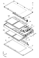
- FIG. 1 is a perspective view of a power storage module 10 according to the present embodiment
- FIG. 2 is an exploded perspective view of the power storage module 10.
- the X direction, the Y direction, and the Z direction are three directions orthogonal to each other.
- the power storage module 10 includes a frame 11, power storage cells 12 (12A to 12D), a first voltage detection board 13, a second voltage detection board 14, a connector board 15, a first plate 16, A second plate 17, a first heat transfer insulating sheet 18 and a second heat transfer insulating sheet 19 are provided.
- the power storage module 10 includes four power storage cells 12, and each power storage cell 12 is a power storage cell 12A, 12B, 12C, and 12D.
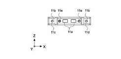
- the frame 11 is a hollow frame-like member and forms a storage space for the storage cell 12. As shown in FIGS. 1 and 2, on one surface of the frame 11, a connector hole 11a, a screw hole 11b, a positive terminal 11c, a negative terminal 11d, and a polarity display 11e are provided. Two connector holes 11a are provided in the frame 11, but one or three or more may be provided.
- Two screw holes 11b are provided in the frame 11, and the positive terminal 11c and the negative terminal 11d are provided around the screw hole 11b.
- One polarity display 11e is provided in the vicinity of the positive terminal 11c and the negative terminal 11d, and indicates the polarity (+ or ⁇ ) of the positive terminal 11c and the negative terminal 11d.
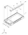
- the frame 11 is formed by insert molding, and has a configuration in which a bus bar 110 is embedded in a resin member made of synthetic resin.
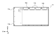
- FIG. 3 is a schematic view of the frame 11 and the bus bar 110, and FIGS. 4 to 6 are plan views of the frame 11 viewed from various directions.
- the bus bar 110 includes five bus bars: a first bus bar 111, a second bus bar 112, a third bus bar 113, a fourth bus bar 114, and a fifth bus bar 115.
- Each bus bar is embedded in the frame 11 in a separated state, and a part thereof is exposed from the frame 11.
- the first bus bar 111 is exposed on the upper surface side (first plate 16 side) of the frame 11 as shown in FIG. 4, and is exposed around one screw hole 11b as shown in FIG. Form.
- the second bus bar 112 is exposed on the lower surface side (the second plate 17 side) of the frame 11, and is exposed around the other screw hole 11b as shown in FIG. Form.
- the third bus bar 113 is exposed at two places on the upper surface side of the frame 11 as shown in FIG. 4, and the fourth bus bar 114 is exposed at two places on the lower surface side of the frame 11 as shown in FIG. As shown in FIGS. 4 and 5, the fifth bus bar 115 is exposed on the upper surface side and the lower surface side of the frame 11.
- the bus bar 110 can be made of copper.
- the bus bar 110 may be made of a highly conductive metal material.
- the storage cell 12 (12A to 12D) is a cell capable of storing and discharging, and is a lithium ion capacitor or a lithium ion secondary battery.
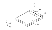
- FIG. 7 is a perspective view of the electricity storage cell 12
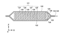
- FIG. 8 is a cross-sectional view of the electricity storage cell 12.
- the electricity storage cell 12 includes an electricity storage element 121, an exterior film 122, a positive electrode tab 123, a negative electrode tab 124, a positive electrode conductor 125, and a negative electrode conductor 126.
- the electricity storage element 121 includes a positive electrode 127, a negative electrode 128, and a separator 129, and the positive electrode 127 and the negative electrode 128 are alternately stacked via the separator 129.
- the positive electrode 127 includes a positive electrode active material, and may be configured by laminating a positive electrode active material on both front and back surfaces of a positive electrode current collector made of metal.
- the positive electrode active material is activated carbon, for example, and can be appropriately changed according to the type of the storage cell 12.
- the negative electrode 128 may be configured by laminating a negative electrode active material on both front and back surfaces of a negative electrode current collector made of metal and including a negative electrode active material.
- the negative electrode active material is a carbon-based material, for example, and can be appropriately changed according to the type of the storage cell 12.
- the separator 129 is disposed between the positive electrode 127 and the negative electrode 128 and allows the electrolyte to pass therethrough and prevents (insulates) the positive electrode 127 and the negative electrode 128 from contacting each other.
- the separator 129 can be a woven fabric, a nonwoven fabric, a synthetic resin microporous membrane, or the like, and a cellulose-based or polyolefin-based material can be used.
- the number of the positive electrode 127 and the negative electrode 128 constituting the power storage element 121 is not particularly limited as long as the positive electrode 127 and the negative electrode 128 are alternately stacked via the separator 129.
- the electricity storage element 121 is sealed with the exterior film 122 together with the electrolyte.
- the electrolyte is not particularly limited, and can be appropriately changed according to the type of the storage cell 12.
- the exterior film 122 can be a laminate film in which a synthetic resin is laminated on the front and back of a metal foil, and the two exterior films 122 are fused at the periphery of the power storage element 121 to seal the inside.
- a positive electrode tab 123 and a negative electrode tab 124 are sandwiched between the outer film 122 and the outer film 122.
- the positive electrode tab 123 is electrically connected to the positive electrode 127 by a positive electrode conductor 125 that is a wiring or foil
- the negative electrode tab 124 is electrically connected to the negative electrode 128 by a negative electrode conductor 126 that is a wiring or foil.
- the positive electrode tab 123 and the negative electrode tab 124 are made of different metal materials. Specifically, the positive electrode tab 123 can be made of aluminum, and the negative electrode tab 124 can be made of copper. This is because when the storage cell 12 is a lithium ion capacitor or a lithium ion secondary battery, if the positive electrode tab 123 and the negative electrode tab 124 are made of the same metal material, one of them is dissolved by an electrochemical action.
- the power storage module 10 can include four power storage cells 12, but is not limited thereto, and can include one or a plurality of sets in which two power storage modules 10 are stacked in the Z direction. . That is, the power storage module 10 can include an even number of power storage modules 10.
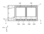
- FIG. 9 is a plan view showing the storage cell 12 housed in the frame 11.
- 10 is a cross-sectional view showing the storage cell 12 accommodated in the frame 11, and is a cross-sectional view taken along the line AA of FIG.
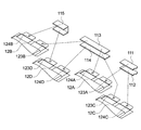
- FIG. 11 is a schematic diagram showing a connection relationship between the positive electrode tab 123 and the negative electrode tab 124 of each power storage cell 12 and the bus bar 110.
- the positive electrode tab 123A of the storage cell 12A is connected to the first bus bar 111, and the negative electrode tab 124A of the storage cell 12A is connected to the third bus bar 113.
- the positive electrode tab 123B of the power storage cell 12B is connected to the third bus bar 113, and the negative electrode tab 124B of the power storage cell 12B is connected to the fifth bus bar 115.
- the positive electrode tab 123C of the storage cell 12C is connected to the fourth bus bar 114, and the negative electrode tab 124C of the storage cell 12C is connected to the second bus bar 112.
- the positive electrode tab 123D of the storage cell 12D is connected to the fifth bus bar 115, and the negative electrode tab 124D of the storage cell 12D is connected to the fourth bus bar 114. Details of the connection between the positive electrode tab 123 and the negative electrode tab 124 of each power storage cell 12 and each bus bar will be described later.
- the first voltage detection board 13 monitors the voltage of the storage cells 12 (12A and 12B) on the first plate 16 side.
- the first voltage detection board 13 is fixed to the frame 11 and is electrically connected to the positive electrode tab 123 and the negative electrode tab 124 of the storage cells 12A and 12B.
- the second voltage detection board 14 monitors the voltage of the storage cell 12 (12C and 12D) on the second plate 17 side.
- the second voltage detection board 14 is fixed to the frame 11 and is electrically connected to the positive electrode tab 123 and the negative electrode tab 124 of the storage cells 12C and 12D.
- the connector board 15 includes a connector 151, a connector 152, a signal processing circuit, and the like.
- the connector 151 is connected to the first voltage detection board 13 and the second voltage detection board 14 through wiring, and the voltage detected in each storage cell 12 is input.
- the connector 152 is inserted through the connector hole 11a and connected to an external device for inspection.
- the first plate 16 is a flat plate member made of a metal material such as aluminum, and is joined to the frame 11.
- the first plate 16 can be screwed to the frame 11 with screws, but may be joined to the frame 11 by other fixing methods.
- the second plate 17 is a flat plate member made of a metal material such as aluminum, and is joined to the frame 11.
- the second plate 17 can be screwed to the frame 11 with screws, but may be joined to the frame 11 by other fixing methods.
- the first heat transfer insulating sheet 18 is a sheet-like member affixed to the first plate 16, and is made of a material having high thermal conductivity and insulation. When the first plate 16 is fixed to the frame 11, the first heat transfer insulating sheet 18 is sandwiched between the storage cells 12 (12 ⁇ / b> A and 12 ⁇ / b> B) on the first plate 16 side and the first plate 16. Heat is transferred to the first plate 16.
- the second heat transfer insulating sheet 19 is a sheet-like member affixed to the second plate 17, and is made of a material having high thermal conductivity and insulation.
- the second heat transfer insulating sheet 19 is sandwiched between the storage cells 12 (12 ⁇ / b> C and 12 ⁇ / b> D) on the second plate 17 side and the second plate 17. Heat is transferred to the second plate 17
- the positive electrode tab 123 and the negative electrode tab 124 of each power storage cell 12 are connected to the bus bar 110. Since the positive electrode tab 123 and the negative electrode tab 124 are made of different metal materials, at least one of them is made of a metal material different from that of the bus bar 110. Specifically, the bus bar 110 may be made of copper, but the positive electrode tab 123 may be made of aluminum.
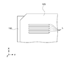
- the positive electrode tab 123 and the negative electrode tab 124 are welded to the bus bar 110 (any one of the first bus bar 111 to the fifth bus bar 115) by laser welding.
- FIG. 12 is a schematic view showing a welded portion of the positive electrode tab 123 and the bus bar 110
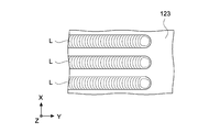
- FIG. 13 is an enlarged view of the welded portion.
- each welding mark L has an arc shape that is continuously arranged in one direction. Is formed.
- the number of the welding marks L is not specifically limited, It selects suitably according to a welding area.
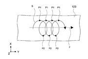
- FIG. 14 and FIG. 15 are schematic diagrams showing laser scanning paths. As shown in these figures, the laser is irradiated on the surface of the positive electrode tab 123 and scanned. Here, the laser is scanned along a scanning path that draws a trajectory that travels in the direction opposite to the direction in which the center proceeds.
- FIG. 14 shows a laser scanning path S and a path F along which the center of the laser travels.
- the same direction as the path F is indicated as a direction P1
- the opposite direction to the path F is indicated as a direction P2.
- the laser is scanned by a scanning path that moves the center of the arc in one direction (path F) while drawing an arc, and a part of the scanning path S travels along the direction P2.
- FIG. 16 is a schematic cross-sectional view of a welded portion between the positive electrode tab 123 and the bus bar 110. As shown in the figure, a material mixing portion M generated by laser welding is formed at the interface between the positive electrode tab 123 and the bus bar 110. The material mixing portion M is a portion where the constituent materials of the positive electrode tab 123 and the bus bar 110 are mixed.
- FIG. 17 is a cross-sectional view showing a welding mark when a member A made of copper and a member B made of aluminum are welded by general laser welding (point welding or wire welding).
- a structure change portion C in which the structure of the member A is changed by welding heat and a structure change portion D in which the structure of the member B is changed by welding heat are formed at the welding location.
- Intermetallic compounds E, which are these compounds, are formed at the interface of the texture change portion D. Due to the intermetallic compound E, the bonding strength between the members A and B is insufficient.
- laser welding is performed using a scanning path that draws an arc continuously but moves the center of the arc in one direction as described above, which increases the welding area, and dissimilar metals are mixed and complicatedly combined. Is done. Thereby, an intermetallic compound does not occur at the interface, and an anchor effect occurs. Therefore, a strong bond is possible even before alloying.
- the laser scanning path is not limited to the above-described scanning path, and the material mixing portion may be formed by providing a scanning path that draws a trajectory that travels in the direction opposite to the direction in which the center proceeds.
- FIG. 18 shows another example of a laser scanning path.
- the scanning path S of the laser is linear, and is a scanning path that draws a trajectory that travels in a direction opposite to the direction in which the laser center advances and in a direction perpendicular to the direction in which the laser center advances. There may be.
- the laser scanning path may alternately repeat the same straight line traveling in one direction and the opposite direction.
- the type of laser used for the above laser welding is not particularly limited. However, a fiber laser capable of drawing a continuous trajectory is preferable.
- the positive electrode tab 123 made of aluminum and the bus bar 110 made of copper are peeled off, the positive electrode tab 123 itself is destroyed, and the welded portion is connected to the bus bar 110, and the welded portion is the base material. It has been confirmed that the strength is exceeded.
- the negative electrode tab 124 and the bus bar 110 can also be laser-welded in the same manner as the positive electrode tab 123.
- the negative electrode tab 124 and the bus bar 110 are made of the same kind of metal material, an intermetallic compound is not formed, and therefore, welding may be performed by a general welding method.
- the positive electrode tab 123 and the bus bar 110 are made of aluminum, and the negative electrode tab 124 is made of copper. Also in this case, by irradiating the negative electrode tab 124 with the laser through the scanning path as described above, a material mixing portion is formed between the negative electrode tab 124 and the bus bar 110, and both are welded with sufficient joint strength.
- the present invention can be applied to the case where the constituent material of at least one of the positive electrode tab 123 and the negative electrode tab 124 is different from the constituent material of the bus bar 110.
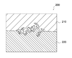
- FIG. 19 is a cross-sectional view of the metal bonded body 200 according to the present embodiment. As shown in the figure, the metal joined body 200 is configured by joining a first member 210 and a second member 220.
- the first member 210 is made of a first metal material
- the second member 220 is made of a second metal material different from the first metal material.
- the first metal material is made of a material having a melting point lower than that of the second metal material
- the first metal material is aluminum (melting point: about 650 ° C.)
- the second metal material is copper (melting point: about 1050 ° C.). Can be.
- the first member 210 and the second member 220 are joined by laser welding, and as shown in FIG. 19, the second metal material is the first metal material at the interface between the first member 210 and the second member 220. I'm stuck inside.
- the first member 210 and the second member 220 include a path in which the first member 210 and the second member 220 are brought into contact with each other, and the first member 210 moves in the direction opposite to the center while moving the center in one direction. Welding is performed by irradiating a laser in the scanning path (see FIG. 14).
- the scanning path of the laser is a scanning path (see FIG. 15) or a straight line that draws a trajectory that travels in a direction opposite to the direction in which the center proceeds, and is opposite to the direction in which the center of the laser travels.
- a scanning path (see FIG. 18) that draws a trajectory that proceeds in a direction perpendicular to the direction in which the center proceeds can be obtained.
- FIG. 20 is a schematic diagram showing a laser welding process.
- the first member 210 when the first member 210 is irradiated with the laser G, the first metal material is melted and a molten pool 210a is formed.
- the surface layer portion of the softened or melted second metal material rises irregularly toward the molten pool 210a (arrow 220a in the figure) and flows into the molten pool 210a by the energy of laser irradiation.
- the first metal material and the second metal material are solidified, and a structure in which the second metal material irregularly enters the first metal material as shown in FIG. 19 is formed. Is done. With this structure, an anchor effect is generated between the first member 210 and the second member 220, and both members are firmly joined.
- the scanning path of the laser G is a scanning path including a path that moves in the opposite direction to the center while moving the center in one direction as described above, and the molten pool 210a is stirred and softened by such a scanning path.
- the rising of the surface layer of the melted second metal material occurs.
- the molten pool 210a is not agitated and the second metal material does not rise.
- two metal members are joined by one laser, but two metal members may be joined by a plurality of laser scans.
- the first member 210 is irradiated with a laser to melt the first metal material, thereby forming a molten pool 210a as shown in FIG.
- the second metal material is softened at the location where the second member 220 contacts the molten pool 210a.
- the molten pool 210a is irradiated with a second laser to stir the molten pool 210a.
- the softened 2nd metal material is mixed with the molten pool 210a.
- the first metal material and the second metal material are solidified, and a structure in which the second metal material irregularly enters the first metal material as shown in FIG. 19 is formed. The With this structure, an anchor effect is generated between the first member 210 and the second member 220, and both members are firmly joined.
- the bus bar 110 is the second member 220 and the positive electrode tab 123 and the negative electrode tab 124 are different in material from the bus bar 110, the first member 210 is used. In comparison with this, the contact resistance between the positive electrode tab 123 or the negative electrode tab 124 and the bus bar 110 is reduced, and the bonding strength can be improved.
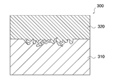
- FIG. 21 is a cross-sectional view of the metal bonded body 300 according to the present embodiment. As shown in the figure, the metal joined body 300 is configured by joining a first member 310 and a second member 320.
- the first metal material composing the first member 310 is made of a material having a melting point lower than that of the second metal material composing the second member 320.
- the first metal material is aluminum (melting point: about 650 ° C.)
- the second metal material may be copper (melting point: 1050 ° C.).
- the first member 310 and the second member 320 are joined by laser welding.
- the second metal material is the first metal material at the interface between the first member 310 and the second member 320. I'm stuck inside.
- the first member 310 and the second member 320 include a path in which the first member 310 and the second member 320 are brought into contact with each other, and the second member 320 moves in the direction opposite to the center while moving the center in one direction. Welding is performed by irradiating a laser in the scanning path (see FIG. 14).
- the scanning path of the laser is a scanning path (see FIG. 15) or a straight line that draws a trajectory that travels in a direction opposite to the direction in which the center proceeds, and is opposite to the direction in which the center of the laser travels.
- a scanning path (see FIG. 18) that draws a trajectory that proceeds in a direction perpendicular to the direction in which the center proceeds can be obtained.
- FIG. 22 is a schematic diagram showing a laser welding process.
- the second metal material constituting the second member 320 is melted to form a molten pool 320a.
- the first metal material constituting the first member 310 is also melted to form a molten pool 310a.
- the melting point of the first metal material is smaller than that of the second metal material, the viscosity of the molten pool 310a is lower than the viscosity of the molten pool 320a.
- the second metal material is pushed into the molten pool 310a having a low viscosity by the laser and flows irregularly into the molten pool 320a.
- the first metal material and the second metal material are solidified, and a structure in which the second metal material irregularly enters the first metal material as shown in FIG. 21 is formed. Is done. With this structure, an anchor effect is generated between the first member 310 and the second member 320, and both members are firmly joined.
- the scanning path of the laser G is a scanning path including a path that moves in the opposite direction to the center while moving the center in one direction as described above.
- the second member 320 is used. In comparison with this, the contact resistance between the positive electrode tab 123 or the negative electrode tab 124 and the bus bar 110 is reduced, and the bonding strength can be improved.
- the type of laser used for laser welding is not particularly limited. However, a fiber laser capable of drawing a continuous trajectory is preferable.
- welding is performed by laser irradiation.
- laser irradiation is not necessarily required, and high energy beam irradiation may be used.
- electron beam irradiation instead of laser irradiation.
Landscapes
- Engineering & Computer Science (AREA)
- Power Engineering (AREA)
- Chemical & Material Sciences (AREA)
- Chemical Kinetics & Catalysis (AREA)
- Electrochemistry (AREA)
- General Chemical & Material Sciences (AREA)
- Microelectronics & Electronic Packaging (AREA)
- Manufacturing & Machinery (AREA)
- Inorganic Chemistry (AREA)
- Physics & Mathematics (AREA)
- Optics & Photonics (AREA)
- Materials Engineering (AREA)
- Connection Of Batteries Or Terminals (AREA)
- Electric Double-Layer Capacitors Or The Like (AREA)
- Battery Mounting, Suspending (AREA)
- Laser Beam Processing (AREA)
Abstract
Description
上記蓄電セルは、正極及び負極を有する蓄電素子と、電解質と共に上記蓄電素子を封止する外装フィルムと、第1の金属材料からなり、上記正極に電気的に接続された正極タブと、第2の金属材料からなり、上記負極に電気的に接続された負極タブを備える。
上記フレームは、上記蓄電セルを収容する収容空間を形成し、上記第2の金属材料からなるバスバーを備える。
上記正極タブと上記バスバーは溶接によって互いに接合され、上記正極タブと上記バスバーの界面に、上記第1の金属材料と上記第2の金属材料が混合した材料混合部が形成されている。
上記蓄電セルは、正極及び負極を有する蓄電素子と、電解質と共に上記蓄電素子を封止する外装フィルムと、第1の金属材料からなり、上記正極に電気的に接続された正極タブと、第2の金属材料からなり、上記負極に電気的に接続された負極タブを備える。
上記フレームは、上記蓄電セルを収容する収容空間を形成し、上記第1の金属材料からなるバスバーを備える。
上記負極タブと上記バスバーは溶接によって互いに接合され、上記負極タブと上記バスバーの界面に、上記第1の金属材料と上記第2の金属材料が混合した材料混合部が形成されている。
正極及び負極を有する蓄電素子と、電解質と共に上記蓄電素子を封止する外装フィルムと、第1の金属材料からなり、上記正極に電気的に接続された正極タブと、第2の金属材料からなり、上記負極に電気的に接続された負極タブとを備える蓄電セルを、上記第2の金属材料からなるバスバーを備えるフレームに収容して上記正極タブを上記バスバーに当接させ、
上記正極タブに、中心を一方向に移動させながら中心とは逆向きに移動する経路を含む走査経路で高エネルギー線を照射し、上記正極タブを上記バスバーに溶接する。
正極及び負極を有する蓄電素子と、電解質と共に上記蓄電素子を封止する外装フィルムと、第1の金属材料からなり、上記正極に電気的に接続された正極タブと、第2の金属材料からなり、上記負極に電気的に接続された負極タブとを備える蓄電セルを、上記第2の金属材料からなるバスバーを備えるフレームに収容して上記正極タブを上記バスバーに当接させ、
上記正極タブに、弧を描きながら弧の中心を一方向に移動させる走査経路で高エネルギー線を照射し、上記正極タブを上記バスバーに溶接する。
正極及び負極を有する蓄電素子と、電解質と共に上記蓄電素子を封止する外装フィルムと、第1の金属材料からなり、上記正極に電気的に接続された正極タブと、第2の金属材料からなり、上記負極に電気的に接続された負極タブとを備える蓄電セルを、上記第1の金属材料からなるバスバーを備えるフレームに収容して上記負極タブを上記バスバーに当接させ、
上記負極タブに、中心を一方向に移動させながら中心とは逆向きに移動する経路を含む走査経路で高エネルギー線を照射し、上記負極タブを上記バスバーに溶接する。
正極及び負極を有する蓄電素子と、電解質と共に上記蓄電素子を封止する外装フィルムと、第1の金属材料からなり、上記正極に電気的に接続された正極タブと、第2の金属材料からなり、上記負極に電気的に接続された負極タブとを備える蓄電セルを、上記第1の金属材料からなるバスバーを備えるフレームに収容して上記負極タブを上記バスバーに当接させ、
上記負極タブに、弧を描きながら弧の中心を一方向に移動させる走査経路で高エネルギー線を照射し、上記負極タブを上記バスバーに溶接する。
上記第1の部材は、第1の金属材料からなる。
上記第2の部材は、上記第1の金属材料とは異なる第2の金属材料からなる。
上記第1の部材と上記第2の部材は溶接によって互いに接合され、上記第1の部材と上記第2の部材の界面において、上記第2の金属材料が上記第1の金属材料中に不規則に入り込んでいる。
第1の金属材料からなる第1の部材を上記第1の金属材料とは異なる第2の金属材料に当接させ、
上記第1の部材に、中心を一方向に移動させながら中心とは逆向きに移動する経路を含む走査経路で高エネルギー線を照射し、上記第1の部材を上記第2の部材に溶接する。
前記正極タブに高エネルギー線を照射して前記正極タブに前記第1の金属材料が融解した融解池を形成し、かつ前記バスバーの前記融解池に当接する箇所において前記第2の金属材料を軟化させる。
前記正極タブに高エネルギー線を照射して前記融解池を撹拌し、軟化した前記第2の金属材料を前記融解池に混合させる。
前記第1の部材に高エネルギー線を照射して前記第1の部材に前記第1の金属材料が融解した融解池を形成し、かつ前記第2の部材の前記融解池に当接する箇所において前記第2の金属材料を軟化させる。
前記第1の部材に高エネルギー線を照射して前記融解池を撹拌し、軟化した前記第2の金属材料を前記融解池に混合させる。
図1は、本実施形態に係る蓄電モジュール10の斜視図であり、図2は蓄電モジュール10の分解斜視図である。なお、以下の図面において、X方向、Y方向及びZ方向は互いに直交する三方向である。
上記のように、各蓄電セル12の正極タブ123と負極タブ124は、バスバー110に接続されている。正極タブ123と負極タブ124は、互いに異なる金属材料からなるため、少なくともいずれか一方は、バスバー110とは異なる金属材料からなる。具体的には、バスバー110は銅からなるが、正極タブ123はアルミニウムからなるものとすることができる。
上記説明においては、蓄電モジュールの正極タブ又は負極タブとバスバーのレーザー溶接について説明したが、本実施形態は他の金属部材の接合に利用することも可能である。
11…フレーム
12…蓄電セル
110…バスバー
121…蓄電素子
122…外装フィルム
123…正極タブ
124…負極タブ
127…正極
128…負極
129…セパレータ
200…金属接合体
210…第1部材
220…第2部材
300…金属接合体
310…第1部材
320…第2部材
Claims (17)
- 正極及び負極を有する蓄電素子と、電解質と共に前記蓄電素子を封止する外装フィルムと、第1の金属材料からなり、前記正極に電気的に接続された正極タブと、第2の金属材料からなり、前記負極に電気的に接続された負極タブを備える蓄電セルと、
前記蓄電セルを収容する収容空間を形成し、前記第2の金属材料からなるバスバーを備えるフレームとを具備し、
前記正極タブと前記バスバーは溶接によって互いに接合され、前記正極タブと前記バスバーの界面に、前記第1の金属材料と前記第2の金属材料が混合した材料混合部が形成されている
蓄電モジュール。 - 正極及び負極を有する蓄電素子と、電解質と共に前記蓄電素子を封止する外装フィルムと、第1の金属材料からなり、前記正極に電気的に接続された正極タブと、第2の金属材料からなり、前記負極に電気的に接続された負極タブを備える蓄電セルと、
前記蓄電セルを収容する収容空間を形成し、前記第1の金属材料からなるバスバーを備えるフレームとを具備し、
前記負極タブと前記バスバーは溶接によって互いに接合され、前記負極タブと前記バスバーの界面に、前記第1の金属材料と前記第2の金属材料が混合した材料混合部が形成されている
蓄電モジュール。 - 請求項1又は2に記載の蓄電モジュールであって、
前記第1の金属材料はアルミニウムであり、前記第2の金属材料は銅である
蓄電モジュール。 - 正極及び負極を有する蓄電素子と、電解質と共に前記蓄電素子を封止する外装フィルムと、第1の金属材料からなり、前記正極に電気的に接続された正極タブと、第2の金属材料からなり、前記負極に電気的に接続された負極タブとを備える蓄電セルを、前記第2の金属材料からなるバスバーを備えるフレームに収容して前記正極タブを前記バスバーに当接させ、
前記正極タブに、中心を一方向に移動させながら中心とは逆向きに移動する経路を含む走査経路で高エネルギー線を照射し、前記正極タブを前記バスバーに溶接する
蓄電モジュールの製造方法。 - 正極及び負極を有する蓄電素子と、電解質と共に前記蓄電素子を封止する外装フィルムと、第1の金属材料からなり、前記正極に電気的に接続された正極タブと、第2の金属材料からなり、前記負極に電気的に接続された負極タブとを備える蓄電セルを、前記第2の金属材料からなるバスバーを備えるフレームに収容して前記正極タブを前記バスバーに当接させ、
前記正極タブに、弧を描きながら弧の中心を一方向に移動させる走査経路で高エネルギー線を照射し、前記正極タブを前記バスバーに溶接する
蓄電モジュールの製造方法。 - 正極及び負極を有する蓄電素子と、電解質と共に前記蓄電素子を封止する外装フィルムと、第1の金属材料からなり、前記正極に電気的に接続された正極タブと、第2の金属材料からなり、前記負極に電気的に接続された負極タブとを備える蓄電セルを、前記第1の金属材料からなるバスバーを備えるフレームに収容して前記負極タブを前記バスバーに当接させ、
前記負極タブに、中心を一方向に移動させながら中心とは逆向きに移動する経路を含む走査経路で高エネルギー線を照射し、前記負極タブを前記バスバーに溶接する
蓄電モジュールの製造方法。 - 正極及び負極を有する蓄電素子と、電解質と共に前記蓄電素子を封止する外装フィルムと、第1の金属材料からなり、前記正極に電気的に接続された正極タブと、第2の金属材料からなり、前記負極に電気的に接続された負極タブとを備える蓄電セルを、前記第1の金属材料からなるバスバーを備えるフレームに収容して前記負極タブを前記バスバーに当接させ、
前記負極タブに、弧を描きながら弧の中心を一方向に移動させる走査経路で高エネルギー線を照射し、前記負極タブを前記バスバーに溶接する
蓄電モジュールの製造方法。 - 請求項4から7のうちいずれか一つに記載の蓄電モジュールの製造方法であって、
前記高エネルギー線はファイバーレーザーの照射光である
蓄電モジュールの製造方法。 - 第1の金属材料からなる第1の部材と、
前記第1の金属材料とは異なる第2の金属材料からなる第2の部材と
を具備し、
前記第1の部材と前記第2の部材は溶接によって互いに接合され、前記第1の部材と前記第2の部材の界面において、前記第2の金属材料が前記第1の金属材料中に不規則に入り込んでいる
金属接合体。 - 請求項9に記載の金属接合体であって、
前記第1の金属材料は前記第2の金属材料より融点が低い金属材料である
金属接合体。 - 請求項10に記載の金属接合体であって、
前記第1の金属材料はアルミニウムであり、前記第2の金属材料は銅である
金属接合体。 - 第1の金属材料からなる第1の部材を前記第1の金属材料とは異なる第2の金属材料に当接させ、
前記第1の部材に、中心を一方向に移動させながら中心とは逆向きに移動する経路を含む走査経路で高エネルギー線を照射し、前記第1の部材を前記第2の部材に溶接する
金属接合体の製造方法。 - 請求項12に記載の金属接合体の製造方法であって、
前記第1の部材を前記第2の部材に溶接する工程は、前記第1の部材に、弧を描きながら弧の中心を一方向に移動させる走査経路で高エネルギー線を照射する
金属接合体の製造方法。 - 請求項12又は13に記載の金属接合体であって、
前記第1の金属材料は前記第2の金属材料より融点が低い金属材料である
金属接合体の製造方法。 - 請求項12から14のうちいずれか一つに記載の金属接合体の製造方法であって、
前記高エネルギー線はファイバーレーザーの照射光である
金属接合体の製造方法。 - 正極及び負極を有する蓄電素子と、電解質と共に前記蓄電素子を封止する外装フィルムと、第1の金属材料からなり、前記正極に電気的に接続された正極タブと、第2の金属材料からなり、前記負極に電気的に接続された負極タブとを備える蓄電セルを、前記第2の金属材料からなるバスバーを備えるフレームに収容して前記正極タブを前記バスバーに当接させ、
前記正極タブに高エネルギー線を照射して前記正極タブに前記第1の金属材料が融解した融解池を形成し、かつ前記バスバーの前記融解池に当接する箇所において前記第2の金属材料を軟化させ、
前記正極タブに高エネルギー線を照射して前記融解池を撹拌し、軟化した前記第2の金属材料を前記融解池に混合させる
蓄電モジュールの製造方法。 - 第1の金属材料からなる第1の部材を前記第1の金属材料とは異なる第2の金属材料に当接させ、
前記第1の部材に高エネルギー線を照射して前記第1の部材に前記第1の金属材料が融解した融解池を形成し、かつ前記第2の部材の前記融解池に当接する箇所において前記第2の金属材料を軟化させ、
前記第1の部材に高エネルギー線を照射して前記融解池を撹拌し、軟化した前記第2の金属材料を前記融解池に混合させる
金属接合体の製造方法。
Priority Applications (3)
| Application Number | Priority Date | Filing Date | Title |
|---|---|---|---|
| JP2016564106A JP6110582B1 (ja) | 2015-10-01 | 2016-07-11 | 蓄電モジュールの製造方法 |
| US15/763,754 US20180269459A1 (en) | 2015-10-01 | 2016-07-11 | Electric storage module, manufacturing method for electric storage module, metal joined body, and manufacturing method for metal joined body |
| CN201680058038.1A CN108140494A (zh) | 2015-10-01 | 2016-07-11 | 蓄电组件、蓄电组件的制造方法、金属接合体和金属接合体的制造方法 |
Applications Claiming Priority (4)
| Application Number | Priority Date | Filing Date | Title |
|---|---|---|---|
| JP2015196034 | 2015-10-01 | ||
| JP2015-196034 | 2015-10-01 | ||
| JP2015-224448 | 2015-11-17 | ||
| JP2015224448 | 2015-11-17 |
Publications (1)
| Publication Number | Publication Date |
|---|---|
| WO2017056628A1 true WO2017056628A1 (ja) | 2017-04-06 |
Family
ID=58427364
Family Applications (1)
| Application Number | Title | Priority Date | Filing Date |
|---|---|---|---|
| PCT/JP2016/070409 Ceased WO2017056628A1 (ja) | 2015-10-01 | 2016-07-11 | 蓄電モジュール、蓄電モジュールの製造方法、金属接合体及び金属接合体の製造方法 |
Country Status (4)
| Country | Link |
|---|---|
| US (1) | US20180269459A1 (ja) |
| JP (4) | JP6110582B1 (ja) |
| CN (1) | CN108140494A (ja) |
| WO (1) | WO2017056628A1 (ja) |
Cited By (4)
| Publication number | Priority date | Publication date | Assignee | Title |
|---|---|---|---|---|
| CN113839150A (zh) * | 2020-06-24 | 2021-12-24 | 新普科技股份有限公司 | 电连接点的接合结构、电连接点的接合方法及电池模块 |
| JP2024514912A (ja) * | 2021-11-01 | 2024-04-03 | エルジー エナジー ソリューション リミテッド | バスバー一体型セルフレームを含むバッテリーモジュール |
| WO2025182520A1 (ja) * | 2024-02-26 | 2025-09-04 | パナソニックIpマネジメント株式会社 | 電池パック |
| WO2025182486A1 (ja) * | 2024-02-26 | 2025-09-04 | パナソニックIpマネジメント株式会社 | 電池パック |
Families Citing this family (17)
| Publication number | Priority date | Publication date | Assignee | Title |
|---|---|---|---|---|
| US20200072266A1 (en) * | 2017-05-22 | 2020-03-05 | Eagle Industry Co., Ltd. | Metal joining structure and metal welding method |
| DE102017211263A1 (de) * | 2017-06-19 | 2018-12-20 | Robert Bosch Gmbh | Akkupackvorrichtung |
| DE102017006229B4 (de) * | 2017-07-03 | 2024-02-01 | Monbat New Power GmbH | Verfahren und Vorrichtung zur Herstellung eines Akkumulators und Akkumulator |
| DE102017211982B4 (de) | 2017-07-13 | 2019-04-18 | Trumpf Laser- Und Systemtechnik Gmbh | Verfahren und Vorrichtung zum Fügen von mindestens zwei Werkstücken |
| JP6974104B2 (ja) * | 2017-10-11 | 2021-12-01 | 太陽誘電株式会社 | 蓄電モジュール |
| CN108356414B (zh) * | 2017-12-25 | 2020-01-24 | 武汉凌云光电科技有限责任公司 | 一种激光焊接点的激光路径及激光焊接方法 |
| JP7192363B2 (ja) * | 2018-09-28 | 2022-12-20 | マツダ株式会社 | レーザ溶接方法及びレーザ溶接装置 |
| KR102722633B1 (ko) * | 2019-03-26 | 2024-10-25 | 주식회사 엘지에너지솔루션 | 버스 바 모듈과 그 제조 방법 |
| KR102541537B1 (ko) * | 2019-06-25 | 2023-06-08 | 주식회사 엘지에너지솔루션 | 전지 모듈 및 이를 포함하는 전지팩 |
| KR102798483B1 (ko) * | 2019-08-02 | 2025-04-22 | 주식회사 엘지에너지솔루션 | 표면 패턴이 형성된 버스바 및 이를 포함하는 전지 모듈 |
| KR102895044B1 (ko) | 2020-04-13 | 2025-12-02 | 주식회사 엘지에너지솔루션 | 전지 모듈 및 그 제조 방법 |
| WO2022203469A1 (ko) * | 2021-03-26 | 2022-09-29 | 주식회사 엘지에너지솔루션 | 배터리 팩, 그리고 이를 포함하는 자동차 |
| GB2605410B (en) * | 2021-03-31 | 2025-03-12 | Jaguar Land Rover Ltd | Methods for Welding Components of Battery Modules |
| GB2605412B (en) * | 2021-03-31 | 2025-05-14 | Jaguar Land Rover Ltd | Methods for Welding Components of Battery Modules |
| WO2023140095A1 (ja) * | 2022-01-18 | 2023-07-27 | 株式会社村田製作所 | コンデンサモジュールおよび電力変換装置 |
| PL440257A1 (pl) * | 2022-01-28 | 2023-07-31 | Aic Spółka Akcyjna | Sposób laserowego spawania ogniw galwanicznych w procesie wytwarzania modułu baterii elektrycznej |
| JP7681052B2 (ja) * | 2023-02-21 | 2025-05-21 | プライムプラネットエナジー&ソリューションズ株式会社 | 蓄電デバイスおよびこれを備えた蓄電モジュール |
Citations (3)
| Publication number | Priority date | Publication date | Assignee | Title |
|---|---|---|---|---|
| JP2004178860A (ja) * | 2002-11-25 | 2004-06-24 | Nissan Motor Co Ltd | シート状二次電池の電極接続方法 |
| WO2007063877A1 (ja) * | 2005-12-01 | 2007-06-07 | Nec Corporation | 電気デバイス集合体の製造方法 |
| WO2015104762A1 (ja) * | 2014-01-08 | 2015-07-16 | パナソニックIpマネジメント株式会社 | レーザ溶接方法 |
Family Cites Families (19)
| Publication number | Priority date | Publication date | Assignee | Title |
|---|---|---|---|---|
| JPH0160792U (ja) * | 1987-10-02 | 1989-04-18 | ||
| JP2675951B2 (ja) * | 1992-08-26 | 1997-11-12 | 新日本製鐵株式会社 | 下向きアーク溶接法 |
| JP3238077B2 (ja) * | 1996-08-28 | 2001-12-10 | 新日本製鐵株式会社 | めっき鋼板の重ねレーザ溶接方法 |
| JP2000158170A (ja) * | 1998-11-27 | 2000-06-13 | Amada Co Ltd | 加工ヘッド |
| JP4496563B2 (ja) * | 1999-04-13 | 2010-07-07 | パナソニック株式会社 | 電池の製造方法 |
| JP2002336983A (ja) * | 2001-05-16 | 2002-11-26 | Toto Ltd | 異種金属の接合方法 |
| US7910855B2 (en) * | 2005-09-23 | 2011-03-22 | Lasx Industries, Inc. | No gap laser welding of coated steel |
| FR2921203B1 (fr) * | 2007-09-13 | 2010-09-24 | Batscap Sa | Module pour ensembles de stockage d'energie electrique a barrette de liaison plate |
| JP5623022B2 (ja) * | 2009-03-25 | 2014-11-12 | 国立大学法人熊本大学 | 溶接方法の設計方法、溶接方法及び溶接接合体 |
| JP5570407B2 (ja) * | 2010-03-26 | 2014-08-13 | パナソニック株式会社 | 組電池とその製造方法および電子機器 |
| JP5657307B2 (ja) * | 2010-08-20 | 2015-01-21 | 株式会社東芝 | 溶接方法、電池並びに組電池の製造方法、および、電池 |
| JP5630373B2 (ja) * | 2011-05-19 | 2014-11-26 | 新日鐵住金株式会社 | 耐遅れ破壊特性に優れた鋼板溶接部の製造方法およびその溶接部を有する鋼構造物 |
| JP5651557B2 (ja) * | 2011-08-02 | 2015-01-14 | 日立オートモティブシステムズ株式会社 | 単電池および組電池 |
| WO2013094000A1 (ja) * | 2011-12-19 | 2013-06-27 | 日立ビークルエナジー株式会社 | 電池における溶接構造、その形成方法、二次電池セルおよび二次電池モジュール |
| TWI484881B (zh) * | 2011-12-30 | 2015-05-11 | Uer Technology Corp | 鋰電池與電路板的銲接結構與銲接方法 |
| DE102012008940B4 (de) * | 2012-05-08 | 2022-03-24 | Fraunhofer-Gesellschaft zur Förderung der angewandten Forschung e.V. | Verfahren zum Fügen von mindestens zwei Werkstücken |
| JP2014063696A (ja) * | 2012-09-24 | 2014-04-10 | Hitachi Vehicle Energy Ltd | 蓄電装置およびその製造方法 |
| JP2015047625A (ja) * | 2013-09-03 | 2015-03-16 | 日本アビオニクス株式会社 | レーザスポット溶接方法およびレーザスポット溶接装置 |
| US10010966B2 (en) * | 2014-02-14 | 2018-07-03 | GM Global Technology Operations LLC | Electrode for resistance spot welding of dissimilar metals |
-
2016
- 2016-07-11 CN CN201680058038.1A patent/CN108140494A/zh active Pending
- 2016-07-11 JP JP2016564106A patent/JP6110582B1/ja not_active Expired - Fee Related
- 2016-07-11 WO PCT/JP2016/070409 patent/WO2017056628A1/ja not_active Ceased
- 2016-07-11 US US15/763,754 patent/US20180269459A1/en not_active Abandoned
- 2016-12-27 JP JP2016252469A patent/JP2017098565A/ja active Pending
-
2017
- 2017-03-14 JP JP2017048985A patent/JP6522029B2/ja not_active Expired - Fee Related
- 2017-05-08 JP JP2017092360A patent/JP2017139239A/ja active Pending
Patent Citations (3)
| Publication number | Priority date | Publication date | Assignee | Title |
|---|---|---|---|---|
| JP2004178860A (ja) * | 2002-11-25 | 2004-06-24 | Nissan Motor Co Ltd | シート状二次電池の電極接続方法 |
| WO2007063877A1 (ja) * | 2005-12-01 | 2007-06-07 | Nec Corporation | 電気デバイス集合体の製造方法 |
| WO2015104762A1 (ja) * | 2014-01-08 | 2015-07-16 | パナソニックIpマネジメント株式会社 | レーザ溶接方法 |
Cited By (5)
| Publication number | Priority date | Publication date | Assignee | Title |
|---|---|---|---|---|
| CN113839150A (zh) * | 2020-06-24 | 2021-12-24 | 新普科技股份有限公司 | 电连接点的接合结构、电连接点的接合方法及电池模块 |
| JP2024514912A (ja) * | 2021-11-01 | 2024-04-03 | エルジー エナジー ソリューション リミテッド | バスバー一体型セルフレームを含むバッテリーモジュール |
| JP7827365B2 (ja) | 2021-11-01 | 2026-03-10 | エルジー エナジー ソリューション リミテッド | バスバー一体型セルフレームを含むバッテリーモジュール |
| WO2025182520A1 (ja) * | 2024-02-26 | 2025-09-04 | パナソニックIpマネジメント株式会社 | 電池パック |
| WO2025182486A1 (ja) * | 2024-02-26 | 2025-09-04 | パナソニックIpマネジメント株式会社 | 電池パック |
Also Published As
| Publication number | Publication date |
|---|---|
| JP2017139239A (ja) | 2017-08-10 |
| JP2017098565A (ja) | 2017-06-01 |
| JP6522029B2 (ja) | 2019-05-29 |
| CN108140494A (zh) | 2018-06-08 |
| US20180269459A1 (en) | 2018-09-20 |
| JP2017152703A (ja) | 2017-08-31 |
| JP6110582B1 (ja) | 2017-04-05 |
| JPWO2017056628A1 (ja) | 2017-10-05 |
Similar Documents
| Publication | Publication Date | Title |
|---|---|---|
| JP6110582B1 (ja) | 蓄電モジュールの製造方法 | |
| EP3159953B1 (en) | Battery pack tab welding method | |
| CN100528453C (zh) | 不同金属薄板的焊接方法、双金属薄板接合元件、电气设备和电气设备组件 | |
| JP4829587B2 (ja) | 電気デバイス集合体及びその製造方法 | |
| JP5326125B2 (ja) | 非水電解質二次電池 | |
| JP2011124024A (ja) | 組電池および単電池 | |
| JP2020513148A (ja) | 電極タブの溶接特性を改善した電極及びこれを含む二次電池 | |
| JP2021515957A (ja) | 電極タブ溶接部の圧接部サイズが相異なる電極組立体及びこれを製造する超音波溶接装置 | |
| KR20190016691A (ko) | 전지 모듈 및 그 제조 방법 | |
| JP2009231145A (ja) | 二次電池 | |
| JP4728758B2 (ja) | 電気デバイスモジュールの製造方法及び電気デバイスモジュール | |
| JP6965587B2 (ja) | 電極組立体 | |
| WO2013018551A1 (ja) | 電池 | |
| JP2015015237A (ja) | 組電池 | |
| CN118017165A (zh) | 电芯及用电设备 | |
| JP2019029642A (ja) | 電気化学セルモジュール及び電気化学セルモジュールの製造方法 | |
| JP5197001B2 (ja) | 電気デバイス集合体の製造方法 | |
| CN223638566U (zh) | 电池及电池包 | |
| KR20180060763A (ko) | 셀 리드의 고정구조가 개선된 배터리 팩 | |
| JP2018010843A (ja) | 組電池及び組電池の製造方法 | |
| JP2011204439A (ja) | 組電池、抵抗溶接方法および組電池の製造方法 | |
| JP6613813B2 (ja) | 電極組立体の製造方法および電極組立体 | |
| JPWO2017057691A1 (ja) | 電気化学デバイスとその製造方法 | |
| JP2007257849A (ja) | ラミネート外装扁平形電池の電池モジュール | |
| JP2018056095A (ja) | 組電池 |
Legal Events
| Date | Code | Title | Description |
|---|---|---|---|
| ENP | Entry into the national phase |
Ref document number: 2016564106 Country of ref document: JP Kind code of ref document: A |
|
| 121 | Ep: the epo has been informed by wipo that ep was designated in this application |
Ref document number: 16850805 Country of ref document: EP Kind code of ref document: A1 |
|
| WWE | Wipo information: entry into national phase |
Ref document number: 15763754 Country of ref document: US |
|
| NENP | Non-entry into the national phase |
Ref country code: DE |
|
| 122 | Ep: pct application non-entry in european phase |
Ref document number: 16850805 Country of ref document: EP Kind code of ref document: A1 |