WO2017047355A1 - 基板処理装置、基板処理方法及び記憶媒体 - Google Patents
基板処理装置、基板処理方法及び記憶媒体 Download PDFInfo
- Publication number
- WO2017047355A1 WO2017047355A1 PCT/JP2016/075001 JP2016075001W WO2017047355A1 WO 2017047355 A1 WO2017047355 A1 WO 2017047355A1 JP 2016075001 W JP2016075001 W JP 2016075001W WO 2017047355 A1 WO2017047355 A1 WO 2017047355A1
- Authority
- WO
- WIPO (PCT)
- Prior art keywords
- substrate
- wafer
- peripheral edge
- film
- height distribution
- Prior art date
- Legal status (The legal status is an assumption and is not a legal conclusion. Google has not performed a legal analysis and makes no representation as to the accuracy of the status listed.)
- Ceased
Links
Images











Classifications
-
- H—ELECTRICITY
- H10—SEMICONDUCTOR DEVICES; ELECTRIC SOLID-STATE DEVICES NOT OTHERWISE PROVIDED FOR
- H10P—GENERIC PROCESSES OR APPARATUS FOR THE MANUFACTURE OR TREATMENT OF DEVICES COVERED BY CLASS H10
- H10P76/00—Manufacture or treatment of masks on semiconductor bodies, e.g. by lithography or photolithography
- H10P76/20—Manufacture or treatment of masks on semiconductor bodies, e.g. by lithography or photolithography of masks comprising organic materials
- H10P76/204—Manufacture or treatment of masks on semiconductor bodies, e.g. by lithography or photolithography of masks comprising organic materials of organic photoresist masks
-
- G—PHYSICS
- G03—PHOTOGRAPHY; CINEMATOGRAPHY; ANALOGOUS TECHNIQUES USING WAVES OTHER THAN OPTICAL WAVES; ELECTROGRAPHY; HOLOGRAPHY
- G03F—PHOTOMECHANICAL PRODUCTION OF TEXTURED OR PATTERNED SURFACES, e.g. FOR PRINTING, FOR PROCESSING OF SEMICONDUCTOR DEVICES; MATERIALS THEREFOR; ORIGINALS THEREFOR; APPARATUS SPECIALLY ADAPTED THEREFOR
- G03F7/00—Photomechanical, e.g. photolithographic, production of textured or patterned surfaces, e.g. printing surfaces; Materials therefor, e.g. comprising photoresists; Apparatus specially adapted therefor
- G03F7/16—Coating processes; Apparatus therefor
- G03F7/162—Coating on a rotating support, e.g. using a whirler or a spinner
-
- B—PERFORMING OPERATIONS; TRANSPORTING
- B05—SPRAYING OR ATOMISING IN GENERAL; APPLYING FLUENT MATERIALS TO SURFACES, IN GENERAL
- B05C—APPARATUS FOR APPLYING FLUENT MATERIALS TO SURFACES, IN GENERAL
- B05C11/00—Component parts, details or accessories not specifically provided for in groups B05C1/00 - B05C9/00
- B05C11/02—Apparatus for spreading or distributing liquids or other fluent materials already applied to a surface ; Controlling means therefor; Control of the thickness of a coating by spreading or distributing liquids or other fluent materials already applied to the coated surface
- B05C11/08—Spreading liquid or other fluent material by manipulating the work, e.g. tilting
-
- B—PERFORMING OPERATIONS; TRANSPORTING
- B05—SPRAYING OR ATOMISING IN GENERAL; APPLYING FLUENT MATERIALS TO SURFACES, IN GENERAL
- B05C—APPARATUS FOR APPLYING FLUENT MATERIALS TO SURFACES, IN GENERAL
- B05C9/00—Apparatus or plant for applying liquid or other fluent material to surfaces by means not covered by any preceding group, or in which the means of applying the liquid or other fluent material is not important
- B05C9/08—Apparatus or plant for applying liquid or other fluent material to surfaces by means not covered by any preceding group, or in which the means of applying the liquid or other fluent material is not important for applying liquid or other fluent material and performing an auxiliary operation
- B05C9/14—Apparatus or plant for applying liquid or other fluent material to surfaces by means not covered by any preceding group, or in which the means of applying the liquid or other fluent material is not important for applying liquid or other fluent material and performing an auxiliary operation the auxiliary operation involving heating or cooling
-
- G—PHYSICS
- G01—MEASURING; TESTING
- G01B—MEASURING LENGTH, THICKNESS OR SIMILAR LINEAR DIMENSIONS; MEASURING ANGLES; MEASURING AREAS; MEASURING IRREGULARITIES OF SURFACES OR CONTOURS
- G01B11/00—Measuring arrangements characterised by the use of optical techniques
- G01B11/02—Measuring arrangements characterised by the use of optical techniques for measuring length, width or thickness
- G01B11/022—Measuring arrangements characterised by the use of optical techniques for measuring length, width or thickness by means of tv-camera scanning
-
- G—PHYSICS
- G01—MEASURING; TESTING
- G01B—MEASURING LENGTH, THICKNESS OR SIMILAR LINEAR DIMENSIONS; MEASURING ANGLES; MEASURING AREAS; MEASURING IRREGULARITIES OF SURFACES OR CONTOURS
- G01B11/00—Measuring arrangements characterised by the use of optical techniques
- G01B11/02—Measuring arrangements characterised by the use of optical techniques for measuring length, width or thickness
- G01B11/06—Measuring arrangements characterised by the use of optical techniques for measuring length, width or thickness for measuring thickness ; e.g. of sheet material
-
- G—PHYSICS
- G01—MEASURING; TESTING
- G01B—MEASURING LENGTH, THICKNESS OR SIMILAR LINEAR DIMENSIONS; MEASURING ANGLES; MEASURING AREAS; MEASURING IRREGULARITIES OF SURFACES OR CONTOURS
- G01B11/00—Measuring arrangements characterised by the use of optical techniques
- G01B11/24—Measuring arrangements characterised by the use of optical techniques for measuring contours or curvatures
- G01B11/2433—Measuring arrangements characterised by the use of optical techniques for measuring contours or curvatures for measuring outlines by shadow casting
-
- G—PHYSICS
- G03—PHOTOGRAPHY; CINEMATOGRAPHY; ANALOGOUS TECHNIQUES USING WAVES OTHER THAN OPTICAL WAVES; ELECTROGRAPHY; HOLOGRAPHY
- G03F—PHOTOMECHANICAL PRODUCTION OF TEXTURED OR PATTERNED SURFACES, e.g. FOR PRINTING, FOR PROCESSING OF SEMICONDUCTOR DEVICES; MATERIALS THEREFOR; ORIGINALS THEREFOR; APPARATUS SPECIALLY ADAPTED THEREFOR
- G03F7/00—Photomechanical, e.g. photolithographic, production of textured or patterned surfaces, e.g. printing surfaces; Materials therefor, e.g. comprising photoresists; Apparatus specially adapted therefor
- G03F7/004—Photosensitive materials
- G03F7/09—Photosensitive materials characterised by structural details, e.g. supports, auxiliary layers
- G03F7/11—Photosensitive materials characterised by structural details, e.g. supports, auxiliary layers having cover layers or intermediate layers, e.g. subbing layers
-
- G—PHYSICS
- G03—PHOTOGRAPHY; CINEMATOGRAPHY; ANALOGOUS TECHNIQUES USING WAVES OTHER THAN OPTICAL WAVES; ELECTROGRAPHY; HOLOGRAPHY
- G03F—PHOTOMECHANICAL PRODUCTION OF TEXTURED OR PATTERNED SURFACES, e.g. FOR PRINTING, FOR PROCESSING OF SEMICONDUCTOR DEVICES; MATERIALS THEREFOR; ORIGINALS THEREFOR; APPARATUS SPECIALLY ADAPTED THEREFOR
- G03F7/00—Photomechanical, e.g. photolithographic, production of textured or patterned surfaces, e.g. printing surfaces; Materials therefor, e.g. comprising photoresists; Apparatus specially adapted therefor
- G03F7/16—Coating processes; Apparatus therefor
- G03F7/168—Finishing the coated layer, e.g. drying, baking, soaking
-
- G—PHYSICS
- G03—PHOTOGRAPHY; CINEMATOGRAPHY; ANALOGOUS TECHNIQUES USING WAVES OTHER THAN OPTICAL WAVES; ELECTROGRAPHY; HOLOGRAPHY
- G03F—PHOTOMECHANICAL PRODUCTION OF TEXTURED OR PATTERNED SURFACES, e.g. FOR PRINTING, FOR PROCESSING OF SEMICONDUCTOR DEVICES; MATERIALS THEREFOR; ORIGINALS THEREFOR; APPARATUS SPECIALLY ADAPTED THEREFOR
- G03F7/00—Photomechanical, e.g. photolithographic, production of textured or patterned surfaces, e.g. printing surfaces; Materials therefor, e.g. comprising photoresists; Apparatus specially adapted therefor
- G03F7/26—Processing photosensitive materials; Apparatus therefor
-
- H—ELECTRICITY
- H10—SEMICONDUCTOR DEVICES; ELECTRIC SOLID-STATE DEVICES NOT OTHERWISE PROVIDED FOR
- H10P—GENERIC PROCESSES OR APPARATUS FOR THE MANUFACTURE OR TREATMENT OF DEVICES COVERED BY CLASS H10
- H10P14/00—Formation of materials, e.g. in the shape of layers or pillars
- H10P14/60—Formation of materials, e.g. in the shape of layers or pillars of insulating materials
- H10P14/63—Formation of materials, e.g. in the shape of layers or pillars of insulating materials characterised by the formation processes
- H10P14/6326—Deposition processes
- H10P14/6342—Liquid deposition, e.g. spin-coating, sol-gel techniques or spray coating
-
- H—ELECTRICITY
- H10—SEMICONDUCTOR DEVICES; ELECTRIC SOLID-STATE DEVICES NOT OTHERWISE PROVIDED FOR
- H10P—GENERIC PROCESSES OR APPARATUS FOR THE MANUFACTURE OR TREATMENT OF DEVICES COVERED BY CLASS H10
- H10P14/00—Formation of materials, e.g. in the shape of layers or pillars
- H10P14/60—Formation of materials, e.g. in the shape of layers or pillars of insulating materials
- H10P14/65—Formation of materials, e.g. in the shape of layers or pillars of insulating materials characterised by treatments performed before or after the formation of the materials
- H10P14/6502—Formation of materials, e.g. in the shape of layers or pillars of insulating materials characterised by treatments performed before or after the formation of the materials of treatments performed before formation of the materials
- H10P14/6508—Formation of materials, e.g. in the shape of layers or pillars of insulating materials characterised by treatments performed before or after the formation of the materials of treatments performed before formation of the materials by exposure to a liquid
-
- H—ELECTRICITY
- H10—SEMICONDUCTOR DEVICES; ELECTRIC SOLID-STATE DEVICES NOT OTHERWISE PROVIDED FOR
- H10P—GENERIC PROCESSES OR APPARATUS FOR THE MANUFACTURE OR TREATMENT OF DEVICES COVERED BY CLASS H10
- H10P14/00—Formation of materials, e.g. in the shape of layers or pillars
- H10P14/60—Formation of materials, e.g. in the shape of layers or pillars of insulating materials
- H10P14/69—Inorganic materials
- H10P14/6902—Inorganic materials composed of carbon, e.g. alpha-C, diamond or hydrogen doped carbon
-
- H—ELECTRICITY
- H10—SEMICONDUCTOR DEVICES; ELECTRIC SOLID-STATE DEVICES NOT OTHERWISE PROVIDED FOR
- H10P—GENERIC PROCESSES OR APPARATUS FOR THE MANUFACTURE OR TREATMENT OF DEVICES COVERED BY CLASS H10
- H10P72/00—Handling or holding of wafers, substrates or devices during manufacture or treatment thereof
- H10P72/04—Apparatus for manufacture or treatment
- H10P72/0448—Apparatus for applying a liquid, a resin, an ink or the like
-
- H—ELECTRICITY
- H10—SEMICONDUCTOR DEVICES; ELECTRIC SOLID-STATE DEVICES NOT OTHERWISE PROVIDED FOR
- H10P—GENERIC PROCESSES OR APPARATUS FOR THE MANUFACTURE OR TREATMENT OF DEVICES COVERED BY CLASS H10
- H10P72/00—Handling or holding of wafers, substrates or devices during manufacture or treatment thereof
- H10P72/04—Apparatus for manufacture or treatment
- H10P72/0451—Apparatus for manufacturing or treating in a plurality of work-stations
- H10P72/0452—Apparatus for manufacturing or treating in a plurality of work-stations characterised by the layout of the process chambers
- H10P72/0458—Apparatus for manufacturing or treating in a plurality of work-stations characterised by the layout of the process chambers vertical arrangement
-
- H—ELECTRICITY
- H10—SEMICONDUCTOR DEVICES; ELECTRIC SOLID-STATE DEVICES NOT OTHERWISE PROVIDED FOR
- H10P—GENERIC PROCESSES OR APPARATUS FOR THE MANUFACTURE OR TREATMENT OF DEVICES COVERED BY CLASS H10
- H10P72/00—Handling or holding of wafers, substrates or devices during manufacture or treatment thereof
- H10P72/06—Apparatus for monitoring, sorting, marking, testing or measuring
- H10P72/0604—Process monitoring, e.g. flow or thickness monitoring
-
- H—ELECTRICITY
- H10—SEMICONDUCTOR DEVICES; ELECTRIC SOLID-STATE DEVICES NOT OTHERWISE PROVIDED FOR
- H10P—GENERIC PROCESSES OR APPARATUS FOR THE MANUFACTURE OR TREATMENT OF DEVICES COVERED BY CLASS H10
- H10P72/00—Handling or holding of wafers, substrates or devices during manufacture or treatment thereof
- H10P72/06—Apparatus for monitoring, sorting, marking, testing or measuring
- H10P72/0606—Position monitoring, e.g. misposition detection or presence detection
-
- H—ELECTRICITY
- H10—SEMICONDUCTOR DEVICES; ELECTRIC SOLID-STATE DEVICES NOT OTHERWISE PROVIDED FOR
- H10P—GENERIC PROCESSES OR APPARATUS FOR THE MANUFACTURE OR TREATMENT OF DEVICES COVERED BY CLASS H10
- H10P72/00—Handling or holding of wafers, substrates or devices during manufacture or treatment thereof
- H10P72/06—Apparatus for monitoring, sorting, marking, testing or measuring
- H10P72/0616—Monitoring of warpages, curvatures, damages, defects or the like
-
- H—ELECTRICITY
- H10—SEMICONDUCTOR DEVICES; ELECTRIC SOLID-STATE DEVICES NOT OTHERWISE PROVIDED FOR
- H10P—GENERIC PROCESSES OR APPARATUS FOR THE MANUFACTURE OR TREATMENT OF DEVICES COVERED BY CLASS H10
- H10P72/00—Handling or holding of wafers, substrates or devices during manufacture or treatment thereof
- H10P72/30—Handling or holding of wafers, substrates or devices during manufacture or treatment thereof for conveying, e.g. between different workstations
- H10P72/33—Handling or holding of wafers, substrates or devices during manufacture or treatment thereof for conveying, e.g. between different workstations into and out of processing chamber
- H10P72/3302—Mechanical parts of transfer devices
-
- H—ELECTRICITY
- H10—SEMICONDUCTOR DEVICES; ELECTRIC SOLID-STATE DEVICES NOT OTHERWISE PROVIDED FOR
- H10P—GENERIC PROCESSES OR APPARATUS FOR THE MANUFACTURE OR TREATMENT OF DEVICES COVERED BY CLASS H10
- H10P72/00—Handling or holding of wafers, substrates or devices during manufacture or treatment thereof
- H10P72/30—Handling or holding of wafers, substrates or devices during manufacture or treatment thereof for conveying, e.g. between different workstations
- H10P72/34—Handling or holding of wafers, substrates or devices during manufacture or treatment thereof for conveying, e.g. between different workstations the wafers being stored in a carrier, involving loading and unloading
- H10P72/3402—Mechanical parts of transfer devices
-
- H—ELECTRICITY
- H10—SEMICONDUCTOR DEVICES; ELECTRIC SOLID-STATE DEVICES NOT OTHERWISE PROVIDED FOR
- H10P—GENERIC PROCESSES OR APPARATUS FOR THE MANUFACTURE OR TREATMENT OF DEVICES COVERED BY CLASS H10
- H10P72/00—Handling or holding of wafers, substrates or devices during manufacture or treatment thereof
- H10P72/50—Handling or holding of wafers, substrates or devices during manufacture or treatment thereof for positioning, orientation or alignment
- H10P72/53—Handling or holding of wafers, substrates or devices during manufacture or treatment thereof for positioning, orientation or alignment using optical controlling means
-
- H—ELECTRICITY
- H10—SEMICONDUCTOR DEVICES; ELECTRIC SOLID-STATE DEVICES NOT OTHERWISE PROVIDED FOR
- H10P—GENERIC PROCESSES OR APPARATUS FOR THE MANUFACTURE OR TREATMENT OF DEVICES COVERED BY CLASS H10
- H10P76/00—Manufacture or treatment of masks on semiconductor bodies, e.g. by lithography or photolithography
- H10P76/20—Manufacture or treatment of masks on semiconductor bodies, e.g. by lithography or photolithography of masks comprising organic materials
-
- H—ELECTRICITY
- H10—SEMICONDUCTOR DEVICES; ELECTRIC SOLID-STATE DEVICES NOT OTHERWISE PROVIDED FOR
- H10P—GENERIC PROCESSES OR APPARATUS FOR THE MANUFACTURE OR TREATMENT OF DEVICES COVERED BY CLASS H10
- H10P76/00—Manufacture or treatment of masks on semiconductor bodies, e.g. by lithography or photolithography
- H10P76/20—Manufacture or treatment of masks on semiconductor bodies, e.g. by lithography or photolithography of masks comprising organic materials
- H10P76/204—Manufacture or treatment of masks on semiconductor bodies, e.g. by lithography or photolithography of masks comprising organic materials of organic photoresist masks
- H10P76/2041—Photolithographic processes
- H10P76/2043—Photolithographic processes using an anti-reflective coating
-
- H—ELECTRICITY
- H10—SEMICONDUCTOR DEVICES; ELECTRIC SOLID-STATE DEVICES NOT OTHERWISE PROVIDED FOR
- H10P—GENERIC PROCESSES OR APPARATUS FOR THE MANUFACTURE OR TREATMENT OF DEVICES COVERED BY CLASS H10
- H10P74/00—Testing or measuring during manufacture or treatment of wafers, substrates or devices
- H10P74/20—Testing or measuring during manufacture or treatment of wafers, substrates or devices characterised by the properties tested or measured, e.g. structural or electrical properties
- H10P74/203—Structural properties, e.g. testing or measuring thicknesses, line widths, warpage, bond strengths or physical defects
-
- H—ELECTRICITY
- H10—SEMICONDUCTOR DEVICES; ELECTRIC SOLID-STATE DEVICES NOT OTHERWISE PROVIDED FOR
- H10P—GENERIC PROCESSES OR APPARATUS FOR THE MANUFACTURE OR TREATMENT OF DEVICES COVERED BY CLASS H10
- H10P74/00—Testing or measuring during manufacture or treatment of wafers, substrates or devices
- H10P74/23—Testing or measuring during manufacture or treatment of wafers, substrates or devices characterised by multiple measurements, corrections, marking or sorting processes
Definitions
- the present invention relates to a substrate processing method, a substrate processing apparatus, and a storage medium for forming a lower layer film provided under a resist film.
- a resist pattern is formed on a semiconductor wafer (hereinafter referred to as a wafer) which is a substrate.
- the wafer is transferred to a coating / developing apparatus for applying and developing a resist and subjected to a resist coating process, and then transferred to an exposure apparatus connected to the coating / developing apparatus. And is exposed along a desired pattern.
- the peripheral edge of the wafer surface is configured as an inclined surface that descends outward.
- a wafer in which the film is formed and the film is removed by CMP (Chemical Mechanical Polishing) in the manufacturing process of the semiconductor device until it is carried into the coating and developing apparatus. (Hereinafter, sometimes referred to as a polished wafer) may be carried in.
- the film formation and film removal may be repeated a plurality of times, and as the number of repetitions increases, the height of the upper end of the inclined surface on the inclined surface and the outer edge of the wafer from the upper end of the inclined surface are increased.
- Edge Roll-Off edge roll-off
- leveling correction for tilting the wafer is performed so that the focus surface and the surface of the wafer in the region where the exposure processing is performed are aligned.
- the focus surface and the surface of the wafer are moved by leveling correction on the inner side of the peripheral edge of the wafer. Even if they can be aligned, if the edge roll-off described above is relatively large at the peripheral edge, that is, if the difference in height between the focus surface and the wafer surface is relatively large, defocusing (focal abnormality) will occur. .
- Patent Document 1 describes an exposure apparatus provided with a leveling sensor that measures the height of the surface of a substrate, but does not disclose any technique for solving the above problem.
- the present invention has been made based on such circumstances, and an object of the present invention is to provide a technique capable of preventing an abnormal resist pattern from being formed at the peripheral edge of the substrate.
- the substrate processing apparatus of the present invention is a height distribution acquisition module for acquiring a height distribution along the radial direction of the substrate for the peripheral edge of the surface of the substrate,
- An underlayer film forming module for forming an underlayer film provided in a lower layer of a resist film on the entire surface of the substrate so as to correct a drop in the height of the peripheral edge based on the distribution of the height; It is provided with.
- the storage medium of the present invention is a storage medium storing a computer program used in a substrate processing apparatus for forming a lower layer film provided on a lower layer of a resist film on a substrate, and the program executes the substrate processing method of the present invention. It is characterized in that steps are set up for this purpose.
- the distribution of the height along the radial direction of the substrate is obtained for the peripheral edge portion of the surface of the substrate, and the drop in the height of the peripheral edge portion is corrected based on the distribution of the height.
- a lower layer film is formed on the entire surface of the substrate. Therefore, it is possible to prevent the focus during exposure from deviating from the surface of the resist film formed on the lower layer film at the peripheral edge of the substrate. As a result, the formation of an abnormal resist pattern at the peripheral edge can be suppressed.
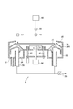
- FIG. 2 is a detailed plan view of the coating and developing apparatus.
- FIG. It is a perspective view of the coating and developing apparatus. It is a schematic longitudinal side view of the coating and developing apparatus. It is a vertical side view of the SOC film formation module provided in the said application
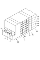
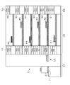
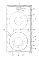
- FIGS. 1, 2, and 3 are a plan view, a perspective view, and a schematic longitudinal side view of the coating and developing apparatus 1, respectively.
- the coating and developing apparatus 1 is configured by connecting a carrier block D1, a processing block D2, and an interface block D3 horizontally and linearly. Further, the exposure apparatus D4 is connected to the interface block D3 on the side opposite to the processing block D2.
- the arrangement direction of the blocks D1 to D3 and the exposure apparatus D4 is the front-rear direction.
- an organic film called SOC Spin On Carbon
- an antireflection film and a resist film are laminated in this order from the lower side on the surface of the wafer W which is a circular substrate, and the resist film is deposited on the exposure apparatus D4. To be exposed. After the exposure process, a resist film is applied and developed by the developing device 1.
- the diameter of the wafer W is 300 mm
- a notch N that is a notch indicating the direction of the wafer W is provided on the periphery of the wafer W.
- the carrier block D ⁇ b> 1 applies a carrier C storing a plurality of wafers W, and carries it in / out of the developing device 1.
- the wafer W in the carrier C is, for example, the polishing wafer described in the background art section. However, a wafer W that has not been subjected to film formation and CMP removal described above (hereinafter may be referred to as a new wafer) may be stored.
- the carrier block D ⁇ b> 1 includes a mounting table 11 for the carrier C, an opening / closing unit 12, and a transfer mechanism 13 for transferring the wafer W from the carrier C via the opening / closing unit 12.
- the processing block D2 is configured by laminating first to sixth unit blocks E1 to E6 for performing liquid processing on the wafer W in order from the bottom.
- E1 and E2 are the same unit blocks
- E3 and E4 are the same unit blocks
- E5 and E6 are the same unit blocks.
- the wafer W is transferred and processed in parallel with each other.
- the unit block E1 as a representative of the unit blocks will be described with reference to FIG.
- a plurality of shelf units U are arranged in the front-rear direction on the left and right sides of the transport area 14 from the carrier block D1 to the interface block D3, and two SOC film forming modules 3 are arranged in the front-rear direction on the other side.
- the SOC film forming module 3 is a module for supplying a chemical solution to the wafer W and forming an organic film called SOC (Spin On Carbon) as a lower layer film on the surface of the wafer W.
- SOC Spin On Carbon
- the shelf unit U includes a heating module 15.
- the transfer area 14 is provided with a transfer arm F1 which is a transfer mechanism for the wafer W.
- the antireflection film forming module 16 and the resist film forming module 17 are used. And.
- the antireflection film forming module 16 and the resist film forming module 17 are configured in substantially the same manner as the SOC film forming module 3, but the chemical solution supplied to the wafer W is different from that of the SOC film forming module 3.
- the film forming module 16 is supplied with a chemical solution for forming an antireflection film, and the resist film forming module 17 is supplied with a resist.
- the unit blocks E5 and E6 include a developing module 18 instead of the SOC film forming module 3.
- the developing module 18 is configured in substantially the same manner as the SOC film forming module 3, but for the chemical solution supplied to the wafer W, the developing solution is supplied to the wafer W instead of the chemical solution for forming the SOC film. Except for such differences, the unit blocks E1 to E6 are configured in the same manner. In FIG. 3, the transfer arms of the unit blocks E2 to E6 corresponding to the transfer arm F1 are indicated as F2 to F6.
- the tower T1 On the carrier block D1 side in the processing block D2, there are provided a tower T1 extending up and down across the unit blocks E1 to E6, and a transport mechanism 19 that can move up and down for delivering the wafer W to the tower T1. ing.
- the tower T1 is composed of a plurality of modules stacked on each other. The modules provided at the respective heights of the unit blocks E1 to E6 are connected to the wafers W between the transfer arms F1 to F6 of the unit blocks E1 to E6. Can be handed over.
- a delivery module TRS provided at the height position of each unit block, a temperature control module CPL for adjusting the temperature of the wafer W, a buffer module for temporarily storing a plurality of wafers W, and a wafer W
- a hydrophobizing module for hydrophobizing the surface of the surface is included.
- the hydrophobic treatment module, the temperature control module, and the buffer module are not shown.
- the imaging module 5 is provided in the tower T1. Imaging of the wafer W is performed by the imaging module 5, and film forming processing is performed on the wafer W by the SOC film forming module 3 under processing conditions corresponding to the imaging result. The imaging module 5 will be described in detail later.
- the interface block D3 includes towers T2, T3, and T4 extending up and down across the unit blocks E1 to E6.
- the interface block D3 transfers the wafer W to and from the tower T2 and the tower T4.
- the interface arm 21 is a transport mechanism that can be moved up and down to transfer the wafer W to the tower T2 and the tower T3.
- An interface arm 22 that is a transfer mechanism that can be moved up and down to perform the transfer, and an interface arm 23 that is a transfer mechanism for transferring the wafer W between the tower T2 and the exposure apparatus D4 are provided.
- the tower T2 includes a delivery module TRS, a buffer module for storing and retaining a plurality of wafers W before exposure processing, a buffer module for storing a plurality of wafers W after exposure processing, and a temperature for adjusting the temperature of the wafers W.
- a delivery module TRS a delivery module for storing and retaining a plurality of wafers W before exposure processing
- a buffer module for storing a plurality of wafers W after exposure processing
- a temperature for adjusting the temperature of the wafers W a temperature adjustment module.
- the control unit 100 is formed of a computer, for example, and has a program storage unit (not shown).
- the program storage unit stores a program in which instructions (step groups) are set so that the wafer W can be processed in each module and the wafer W can be transferred between modules by each transfer mechanism.
- the height distribution at the peripheral edge of the wafer W in the imaging module 5 described later is acquired, and the damper 39 is opened in the SOC film forming module 3 based on the acquired height distribution. Includes degree settings.
- control unit 100 outputs a control signal to each part of the coating / developing apparatus 1 by the program, thereby controlling the operation of each part of the coating / developing apparatus 1.
- This program is stored in the program storage unit while being stored in a storage medium such as a hard disk, a compact disk, a magnetic optical disk, or a memory card.
- reference numeral 31 denotes a spin chuck that holds the wafer W horizontally by adsorbing the central portion of the back surface of the wafer W.
- reference numeral 32 denotes a rotating mechanism for rotating the spin chuck 31, and the rotation of the spin chuck 31 rotates the wafer W around the horizontal axis.
- reference numeral 33 denotes a cup whose upper side opens, and surrounds the periphery of the wafer W placed on the spin chuck 31.
- 34 is a liquid receiving portion that forms the bottom of the cup 33, and forms an annular recess that opens upward.
- reference numeral 35 denotes a liquid guide portion, which is provided below the spin chuck 31 so as to surround the spin chuck 31, and has an inclined surface so as to guide liquid spilled downward from the wafer W to the liquid receiving portion 34. And a vertical wall extending downward from the peripheral edge of the inclined surface.
- 36 is a plate-like liquid guide portion extending obliquely upward from the inner wall of the cup 33, and receives the liquid scattered from the wafer W and guides it to the liquid receiving portion 34.
- 36A is a through-hole penetrating the liquid guide portion 36 in the thickness direction.
- the liquid receiving part 35 is provided with a liquid discharge port 37 for discharging the chemical liquid out of the cup 33 and an exhaust pipe 38 extending upward.
- the exhaust pipe 38 exhausts air from outside the cup 33 into the cup 33.
- the dotted arrows in the figure indicate the flow of the air thus exhausted.
- reference numeral 39 denotes a damper having an adjustable opening degree provided in the exhaust pipe 38, and exhaust is performed from the exhaust pipe 38 with an exhaust amount corresponding to the opening degree of the damper 39.
- reference numeral 41 denotes three pins (only two are shown in FIG. 4) that can be raised and lowered around the spin chuck 31.
- the wafer W is transferred between the transfer arm F1 or F2 and the spin chuck 31.
- reference numeral 42 denotes a nozzle that discharges the chemical solution for forming the SOC film vertically downward, and is configured to be movable between the center portion of the wafer W held by the spin chuck 31 and the outside of the cup 33.
- reference numeral 43 denotes a chemical solution supply source connected to the nozzle 42 via a chemical solution supply pipe 44.
- reference numeral 45 denotes a flow rate adjusting unit interposed in the chemical solution supply pipe 44 and adjusts the flow rate of the chemical solution supplied to the nozzle 42.
- a chemical solution is discharged from the nozzle 42 to the center of the wafer W held by the spin chuck 31 to start the film forming process.
- the discharged chemical solution is spread on the peripheral edge of the wafer W by the centrifugal force of the rotating wafer W, and is applied to the entire surface of the wafer W, so-called spin coating is performed.
- the rotation of the wafer W is continued in order to dry the chemical liquid and form the SOC film. Thereafter, the rotation of the wafer W is stopped and the film forming process is completed.
- the peripheral edge of the wafer W in the period from the time when the chemical solution reaches the peripheral edge of the wafer W by the spin coating to the predetermined time when the SOC film is not sufficiently dried (referred to as the chemical solution drying period)
- the film thickness distribution of the SOC film along the radial direction of the wafer W at the peripheral edge of the wafer W after the film formation is completed corresponds to the drying speed of the chemical solution. Since the velocity of the airflow at the peripheral edge of the wafer W during the chemical solution drying period depends on the opening of the damper 39, the SOC film at the peripheral edge of the wafer W depends on the opening of the damper 39. The thickness distribution is determined.
- the damper 39 constitutes an adjustment mechanism that adjusts the drying speed of the chemical solution.
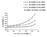
- the opening degree of the damper 39 is set to any one of the first opening degree, the second opening degree, and the third opening degree, and the film forming process is performed. It can be performed. That is, the SOC film forming module 3 can select the film thickness distribution of the SOC film formed for each wafer W. As the order of the magnitudes of the opening degrees, the first opening degree> the second opening degree> the third opening degree. Further, by setting the first opening, the second opening, and the third opening, the SOC along the radial direction of the wafer W formed at the peripheral edge of the wafer W after the film forming process is completed.
- the film thickness distributions of the films are a first film thickness distribution, a second film thickness distribution, and a third film thickness distribution, respectively.
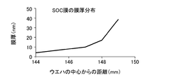
- the graph of FIG. 5 is a graph showing an example of the first to third film thickness distributions.
- the horizontal axis of the graph is the distance from the center of the wafer W (unit: mm), and the vertical axis of the graph is the film thickness (unit: nm) of the formed SOC film.
- the larger the opening degree of the damper 39 the larger the film thickness at the peripheral edge of the wafer W, and the larger the increase in film thickness when viewed outward of the wafer W.
- the reason why the SOC film forming module 3 is configured to be able to select the film thickness distribution formed for each wafer W as described above will be described with reference to FIGS.
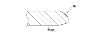
- an inclined surface 10 that descends outward is formed at the peripheral edge of the surface of the wafer W that is transferred to the coating and developing apparatus 1 (see FIG. 6).
- the shape of the peripheral end, more specifically, the height distribution at the peripheral end including the inclined surface 10 along the radial direction of the surface of the wafer W is different for each wafer W.
- the solid line indicates the height distribution of the wafer W1, which is a polishing wafer
- the dotted line indicates the height distribution of the wafer W2, which is a new wafer.
- the horizontal axis of the graph indicates the distance (unit: mm) from the center of the wafer W.
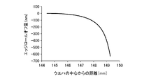
- the vertical axis of the graph represents the edge roll-off amount. The vertical axis will be described in more detail.
- the height of the surface at each position of the peripheral end portion is shown by assuming that the upper surface of the inclined surface 10 and the surface inside the wafer W from the inclined surface 10 are 0 mm. Therefore, in the graph of FIG.
- the edge roll-off amount is 0 or ⁇ (negative), and the larger the absolute value of the edge roll-off amount, the greater the drop from the upper end of the inclined surface 10.
- the wafer W1 and the wafer W2 are different from each other in the height distribution of the peripheral edge, and the wafer W1 has an absolute value of the edge roll-off amount at the same distance from the center of the wafer W. Is bigger. Note that the wafer W in FIG. 6 represents the wafer W1.
- the absolute value of the edge roll-off amount is relatively large in the wafer W1
- the absolute value of the edge roll-off amount becomes large as before the formation of each film.
- the difference between the focus surface at the time of exposure in the exposure apparatus D4 and the resist film becomes large, and defocusing may occur.
- the surface of the SOC film on the inclined surface 10 is less inclined than the inclined surface 10 according to the height distribution at the peripheral edge portion of the surface of the wafer W, and the flatness is improved.
- An SOC film having a film thickness distribution in which the film thickness increases toward the peripheral edge of the wafer W is formed so as to increase.
- an SOC film is formed on the wafer W1 having the height distribution shown in FIG. 7 so that the film thickness distribution along the radial direction at the peripheral edge is shown by the graph in FIG. The horizontal axis and vertical axis of the graph of FIG.
- the film thickness distribution formed on the wafer W by the SOC film forming module 3 is the first to third film thickness distributions shown in FIG. 5, but in FIG.
- the film thickness distribution of the SOC film is different from the third film thickness distribution.
- the graph of FIG. 9 shows the SOC film along the radial direction of the wafer W when the SOC film having the film thickness distribution shown in FIG. 8 is formed on the wafer W1 having the height distribution of the peripheral edge shown in FIG.
- the surface height distribution is indicated by a solid line.
- the horizontal and vertical axes in FIG. 9 indicate the distance from the center of the wafer W and the edge roll-off amount, respectively, as in FIG.
- the surface height distribution of the SOC film in FIG. 9 is the edge roll-off amount at the same distance from the center of the wafer W with respect to the height distribution of the peripheral edge in FIG. 7 and the film thickness distribution of the SOC film in FIG. And the film thickness of the SOC film.
- the height distribution of the peripheral edge before forming the SOC film is shown by a dotted line for comparison.
- the distribution represented by the dotted line is the same as that represented by the solid line in the graph of FIG.
- edge roll-off (height drop) is corrected at the peripheral edge of the wafer W, and an SOC film having a higher surface flatness than the inclined surface 10 is formed on the inclined surface 10.
- the SOC film By forming the SOC film in this way, when the antireflection film and the resist film are laminated on the SOC film, the edge roll-off of the resist film at the peripheral edge portion of the wafer W is suppressed, and defocusing occurs. Can be prevented.
- FIGS. 6 to 9 show an example in which the SOC film is formed on the polished wafer W1 to correct the edge roll-off.
- the edge roll-off is formed by forming the SOC film on the new wafer W2. May be corrected.
- the imaging module 5 which is a height distribution acquisition module will be described with reference to the longitudinal side view and the cross-sectional plan view of FIGS.
- the imaging module 5 captures an image of the peripheral edge of the wafer W so that the control unit 100 can acquire a height distribution along the radial direction at the peripheral edge of the surface of the wafer W, and controls the image data.
- 51 is a housing
- 52 is a transfer port for the wafer W opened in the side wall of the housing 51.
- Reference numeral 53 denotes a stage for attracting the central portion of the back surface of the wafer W and placing the wafer W horizontally, and is rotatable by the drive mechanism 54 and between the front side (conveying port 52 side) and the back side of the housing 51. It is configured to be movable.
- reference numeral 55 denotes an elevating pin for delivering the wafer W between the transfer mechanism 19 and the stage 53 which is the first placement unit.
- reference numeral 56 denotes a transmissive photoelectric sensor, which includes a light projecting unit 56A positioned above the stage 53 and a light receiving unit 56B positioned below the stage 53.
- the stage 53 slightly advances from the position (the position indicated by the solid line in FIG. 10) from which the wafer W is received from the transport mechanism 19 and makes one rotation, and a part of the wafer is directed downward from the light projecting unit 56A during this rotation.
- Light is irradiated so that it is blocked by the peripheral edge of W and the other part passes through the side of the wafer W and is irradiated to the light receiving unit 56B.
- the control unit 100 detects the notch N based on the amount of light received by the light receiving unit 56B.
- a mirror 57 and a camera 58 are provided on the inner side of the housing 51.
- a two-dot chain arrow with 58A in the figure indicates the optical axis of the camera 58, and the optical axis 58A directed downward from the camera 58 is reflected by the mirror 57 and travels in the horizontal direction.
- the optical axis 58A directed in the horizontal direction as described above coincides with an extension line of the diameter of the wafer W at an imaging position where the imaging is performed (a position indicated by a one-dot chain line in the drawing). Can be imaged.
- a camera 59 as a first imaging mechanism is provided in the casing 51.
- a two-dot chain arrow with 59A in the figure indicates the optical axis of the camera 59 and is along the tangential direction of the wafer W.
- the camera 59 can image the side edge of the wafer W at the above-described imaging position from the side of the wafer W.
- this imaging module 5 in addition to the cameras 58 and 59, in order to inspect the state of the entire surface of the wafer W and inspect for the presence or absence of foreign matter on the peripheral surface of the back surface of the wafer W, Although cameras for taking images are provided, the display of these cameras is omitted in order to prevent complication of illustration and description.
- the imaging of the wafer W in the imaging module 5 and the processing in the control unit 100 until the height distribution of the peripheral edge of the wafer W described above is acquired from the acquired image data will be described.
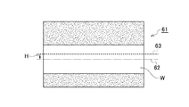
- the wafer W is delivered to the stage 53, the notch N is detected as described above, and the wafer W is rotated so that the notch N is directed in a predetermined direction. Then, the wafer W moves to the imaging position, and imaging is performed by the camera 58 that is the second imaging mechanism, and image data 61 as shown in FIG.
- an upper and lower center position 62 (indicated by a one-dot chain line in the figure) of the wafer W in the image data 61 is detected, and a center position 62 with respect to a preset reference position (indicated by a dotted line in the figure) 63.
- a vertical displacement amount H is calculated. For example, when the peripheral edge of the wafer W is inclined with respect to the horizontal plane due to warpage of the wafer W, the deviation amount H is a value other than 0, and when the peripheral edge of the wafer W is not inclined with respect to the horizontal plane, the deviation amount H is The value is 0. In the example of FIG. 12, the image data 61 in the case where the deviation amount H is a value other than 0 is shown.
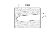
- FIG. 13 shows an example of the image data 64.
- the acquired image data 64 is corrected based on the shift amount H. Specifically, the image data 64 is corrected so that the image is inclined by an amount corresponding to the shift amount H, and the surface of the wafer W inside the inclined surface 10 becomes horizontal.
- FIG. 14 shows the image data 64 corrected in this way.
- the corrected image data 64 for example, the radial direction of the surface of the peripheral edge portion of the wafer W described above shown in the graph of FIG.
- the height distribution along is obtained.
- the horizontal axis and the vertical axis of the graph of FIG. 15 indicate the distance from the center of the wafer W and the edge roll-off amount, respectively, as in the graph of FIG.
- the calculation of the shift amount H, the correction of the image data 64, and the acquisition of the height distribution of the peripheral edge portion of the wafer W based on the corrected image data 64 are performed by the control unit 100 serving as a calculation unit.
- FIG. 16 The wafer W is transferred to one of the unit blocks E with respect to two unit blocks E configured in the same manner.
- the wafers W are transferred to E1, E3, and E5, respectively. It will be described as being done.
- the wafer W having the inclined surface 10 shown in FIG. 6 is transferred from the carrier C to the transfer module TRS0 of the tower T1 in the processing block D2 by the transfer mechanism 13, and then transferred to the imaging module 5 by the transfer mechanism 19.
- the imaging module 5 as described above, detection of the notch N, adjustment of the orientation of the wafer W, acquisition of the image data 61 described in FIG. 12, detection of the vertical displacement amount H of the wafer W based on the image data 61, FIG. Acquisition of the image data 64 at the peripheral edge of the wafer W described in FIG. 14, correction of the image data 64 based on the shift amount H described in FIG. 14, and the wafer at the peripheral edge of the surface of the wafer W described in FIG. Acquisition of the height distribution along the radial direction of W is performed.
- the first to third film thickness distributions of the SOC film described in FIG. 5 and the height distribution of the peripheral edge of the wafer W acquired by the imaging module 5 are described with reference to FIGS.
- the height distribution of the surface of the SOC film is acquired. More specifically, the sum of the film thickness defined by each of the first to third film thickness distributions at the same distance from the center of the wafer and the acquired height of the peripheral edge is calculated.
- the surface height distribution of the SOC film as shown in FIG. 9 is calculated using the first film thickness distribution, calculated using the second film thickness distribution, and the third film thickness distribution. A total of three types are obtained with those calculated using.
- the one having the smallest variation in the film thickness of each portion that is, the one having the highest flatness is determined.
- the film thickness distribution used to calculate the determined height distribution of the surface of the SOC film is determined to form the SOC film.
- the wafer W on which the thickness distribution of the SOC film thus formed is determined is transferred from the imaging module 5 to the transfer module TRS1 of the tower T1 corresponding to the unit block E1 by the transfer mechanism 19, and is transferred to the SOC by the transfer arm F1. It is conveyed to the film forming module 3. Then, as described with reference to FIG. 4, spin coating of the chemical solution is performed, and after the chemical solution has spread from the center portion to the peripheral portion of the surface of the wafer W, the opening degree of the damper 39 is the first to third opening amounts. Of these, the opening is obtained to obtain the determined thickness distribution of the SOC film.
- the chemical solution on the surface of the wafer W is dried by being exposed to the exhaust flow, and the entire surface of the wafer W is adjusted so as to have the determined film thickness distribution among the first to third film thickness distributions at the end of the wafer W.
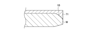
- the SOC film 71 is formed (FIG. 16). That is, the surface of the SOC film 71 is formed on the inclined surface 10 so that edge roll-off is suppressed more than the inclined surface 10.
- the wafer W is transferred to the heating module 15 by the transfer arm F1, heated, and transferred to the delivery module TRS1. Subsequently, the wafer W is transferred by the transfer mechanism 19 to the delivery module TRS3 corresponding to the unit block E3. Then, it is transported to the antireflection film forming module 16 by the transport arm F3, and similar to the processing in the SOC film forming module 3, the chemical solution is applied by spin coating, and the antireflection film 72 is formed on the entire surface of the wafer W.
- the antireflection film 72 is formed so as to have a uniform film thickness at each portion in the plane of the wafer W. As described above, since the edge roll-off of the SOC film 71 below the antireflection film 72 is suppressed at the peripheral edge of the wafer W, the edge rolloff is also suppressed on the surface of the antireflection film 72.
- the wafer W is transported to the heating module 15 by the transport arm F3 and heated, and then transported to the resist film forming module 17, where the resist is applied by spin coating in the same manner as the processing in the SOC film forming module 3.
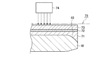
- a resist film 73 is formed on the entire surface of the wafer W (FIG. 17).
- the resist film 73 is also formed so as to have a uniform film thickness at each part in the plane of the wafer W. As described above, since the edge roll-off of the SOC film 71 below the resist film 73 is suppressed at the peripheral edge of the wafer W, the edge roll-off is also suppressed on the surface of the resist film 73.
- the wafer W is transferred by the transfer arm F3 in the order of the heating module 15 ⁇ the delivery module TRS31 of the tower T2. Subsequently, the wafer W is loaded into the exposure apparatus D4 through the tower T3 by the interface arms 21 and 23.
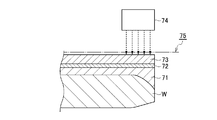
- an exposure head 74 that irradiates an exposure beam moves on the surface of the wafer W, and an exposure process is performed on each area of the wafer W (FIG. 18).
- the dotted arrow in the figure indicates the exposure beam.
- reference numeral 75 denotes a focus surface of the exposure head 74.
- the peripheral edge of the wafer W is suppressed in the state where the deviation between the surface of the resist film 73 and the focus surface 75 is suppressed at the peripheral edge of the wafer W.
- An exposure process can be performed on the region including the part (FIG. 19).
- the exposed wafer W is transported between the towers T2 and T4 by the interface arms 22 and 23, and transported to the transfer module TRS51 of the tower T2 corresponding to the unit block E5.
- the heating module 15 ⁇ the developing module 18 is transported by the transport arm F5. In this order, they are conveyed and developed.
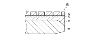
- the exposure is performed so that the deviation between the focus surface 75 and the surface of the resist film 73 is suppressed at the peripheral edge of the wafer W, so that the CD becomes the design value at the peripheral edge of the wafer W.
- a resist pattern 76 is formed (FIG. 20).
- the wafer W is transported in the order of the transport arm F5 ⁇ the heating module 15 ⁇ the transfer module TRS5 of the tower T1 ⁇ the transport mechanism 13 and is returned to the carrier C by the transport mechanism 13.
- the transfer arms F2, F4, and F6 are used, and the unit blocks E1, E3 are used for the transfer modules TRS of the towers T1, T2.
- Modules having heights corresponding to the unit blocks E2, E4, E6 are used instead of modules having heights corresponding to E5.
- the coating / developing apparatus 1 based on the image data 64 obtained by imaging the side edge of the wafer W from the side by the imaging module 5, the wafer W at the peripheral edge of the surface of the wafer W is obtained.
- the opening degree of the damper 39 is obtained by the SOC film forming module 3 so as to acquire the height distribution along the radial direction and correct the height drop at the peripheral edge based on the acquired height distribution. Is set to form the SOC film.
- the resist film is laminated
- the image data 64 acquired by the camera 59 is corrected based on the image data 61 acquired by the camera 58 that captures the side surface of the wafer W, and the corrected image data 64 is corrected. Based on the above, the distribution of the height position of the peripheral edge of the wafer W is acquired. Therefore, since the control unit 100 can grasp the distribution of the height position of the inclined surface 10 more accurately, the SOC film is formed so that the flatness of the surface at the peripheral edge of the wafer W is more reliably increased. be able to.
- the coating / developing apparatus 1 is provided with a module including a reflective laser type displacement sensor 66 shown in FIG.
- the displacement sensor 66 irradiates the laser vertically downward and receives the laser reflected by the wafer W.
- the displacement sensor 66 is connected to a moving mechanism (not shown) so that the displacement sensor 66 can move along the radial direction of the wafer W on the end portion of the wafer W mounted on the mounting portion in the module. Then, the displacement sensor 66 moves while irradiating the peripheral edge of the wafer W including the inclined surface 10 from the displacement sensor 66. Based on the light received by the moving displacement sensor 66, the control unit 100 acquires the height distribution at the peripheral edge of the wafer W surface.
- a laser is intermittently irradiated to the inclined surface 10 during the movement, and a plurality of positions at intervals of the inclined surface 10 are provided.
- the height may be acquired, and the thickness distribution of the SOC film may be determined based on the height.
- the SOC film is formed by spin coating, the film thickness at each position in the circumferential direction is equal. Therefore, when moving the displacement sensor 66 along the radial direction of the wafer W, the wafer W is not limited to being stationary, and the wafer W is rotated to acquire the height distribution of the surface of the peripheral edge. You may go.
- the thickness of each part in the surface of the resist film is not increased so that the thickness of the resist film increases toward the peripheral edge so as to correspond to the height distribution of the inclined surface 10. This is because the resist pattern CD also varies in each part of the surface.
- an antireflection film is formed based on the height distribution of the peripheral edge of the wafer W so as to increase in thickness toward the peripheral edge as in the above-described SOC film, and the peripheral edge of the antireflection film.
- the surface of the part may be flat.
- the film thickness distribution of one of the antireflection film and the SOC film are both adjusted based on the acquired height distribution of the peripheral edge of the wafer W. It may be.
- the antireflection film is used as a hard mask in an etching process which is a post-process of photolithography, it takes a long time to remove by etching if the thickness is large. May be required.
- the SOC film is an organic film, a portion having a relatively large thickness can be quickly removed by plasma treatment using oxygen. Therefore, rather than adjusting the film thickness distribution only for the antireflection film of the SOC film and the antireflection film, only the film thickness distribution is adjusted only for the SOC film, or the film thickness distributions of the SOC film and the antireflection film are both adjusted. It is preferable to adjust so as to suppress an increase in the thickness of the antireflection film.
- the antireflection film that forms the lower layer of the resist film may be made of an organic material, or may be made of an inorganic material such as silicon nitride or silicon oxide.
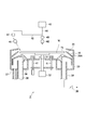
- FIG. 22 shows an example in which the current plate 81 is provided in the SOC film forming module 3.
- the rectifying plate 81 is configured in a ring shape along the peripheral edge so as to cover the peripheral edge of the wafer W. Further, the rectifying plate 81 is configured to be movable up and down by the lifting mechanism 82.
- the current plate 81 is disposed at a height position slightly away from the surface of the wafer W during the chemical solution drying period of the chemical solution described above.
- the diameter of the wafer W flows from the central opening of the current plate 81 to the lower surface of the current plate 81 and between the lower surface of the current plate 81 and the surface of the rotating wafer W.
- the chemical solution at the peripheral edge of the wafer W is dried while being exposed to the exhaust flow flowing along the direction, and the SOC film 71 is formed.
- the thickness can be increased. That is, the thickness distribution of the SOC film 71 at the peripheral edge of the wafer W can be changed by changing the height of the rectifying plate 81. Therefore, during the chemical solution drying period, the flow straightening plate 81 is arranged at a height corresponding to the acquired height distribution of the peripheral end portion of the wafer W, and the chemical solution on the surface of the wafer W is dried, so that the peripheral end portion of the wafer W is obtained. Thus, it is possible to form the SOC film 71 in which edge roll-off is suppressed.
- the SOC film forming module 3 shown in FIG. 23 includes a light irradiation unit 83 formed of LEDs that irradiate light vertically downward on the peripheral end of the wafer W held by the spin chuck 31.
- the light irradiation unit 83 locally heats the peripheral edge of the wafer W by irradiating the wafer W with light.
- the light irradiation intensity by the light irradiation unit 83 can be adjusted. The higher the irradiation intensity, the higher the temperature at the peripheral edge of the wafer W, and the faster the chemical solution is dried.
- the SOC film 71 in which edge roll-off is suppressed can be formed on the peripheral edge of the wafer W by heating the portion so as to have a temperature corresponding to the height distribution.
- the SOC film forming module 3 shown in FIG. 24 includes a nozzle 46 that can locally discharge a chemical solution for forming the SOC film on the peripheral edge of the wafer W.
- reference numeral 47 denotes a chemical liquid flow rate adjusting unit interposed in a chemical liquid supply pipe 48 that connects the nozzle 46 and the chemical liquid supply source 43.
- a chemical solution is applied to the entire surface of the wafer W by spin coating, and the chemical solution is dried to form an SOC film. Then, the chemical solution is supplied from the nozzle 46 to the rotating wafer W. That is, in the SOC film forming module 3 of FIG. 24, the chemical solution for forming the SOC film is applied to the peripheral end portion of the wafer W in an overlapping manner.
- the flow rate of the chemical solution supplied to the nozzle 46 by the flow rate adjustment unit 47 and the rotation speed of the wafer W are controlled based on the acquired height distribution of the peripheral edge of the wafer W, and edge roll-off is suppressed.
- the chemical solution is applied to the peripheral end so as to obtain a desired film thickness.
- edge roll-off at the peripheral edge of the SOC film can be suppressed. Good.
- the device configuration examples described above can be implemented in combination.
- the method of adjusting the film thickness distribution of the SOC film by adjusting the opening degree of the damper 39 and adjusting the irradiation amount from the light irradiation unit 83 has been shown, the opening degree of the damper 39 and the irradiation from the light irradiation unit 83 are shown.
- the film thickness distribution of the SOC film may be adjusted by changing both amounts.
- evaluation test 1 The evaluation test 1 conducted in connection with the present invention will be described.
- An SOC film, an antireflection film, and a resist film were formed on the wafer W whose peripheral edge has a height distribution as shown in the graph of FIG. 25, and a resist pattern was formed by exposure and development.
- the horizontal axis and the vertical axis of the graph indicate the distance from the center of the wafer W and the roll-off amount, respectively, as in the graph of FIG.
- the wafer W used in this evaluation test 1 is a polished wafer.
- the film thickness of each film was different from the above-described embodiment, and the film was formed to be uniform over the entire surface of the wafer W. After forming the resist pattern, the in-plane CD of the wafer W was measured.
- the graph of FIG. 26 shows the measurement result of CD.
- the horizontal and vertical axes of the graph indicate the distance (unit: mm) and CD (unit: nm) from the center of the wafer W, respectively.
- the edge roll-off amount is 0 mm until the distance from the center of the wafer W is 145 mm.
- the absolute value of the edge roll-off amount gradually increases.
- the CD changes at substantially the same value until the distance from the center of the wafer W is 145 mm. A decrease in CD is seen.
- the CD variation corresponds to the edge roll-off amount. Therefore, it is effective to suppress the CD variation by suppressing the edge roll-off by the method described in the embodiment of the present invention.
Landscapes
- Physics & Mathematics (AREA)
- General Physics & Mathematics (AREA)
- Engineering & Computer Science (AREA)
- Architecture (AREA)
- Structural Engineering (AREA)
- Exposure Of Semiconductors, Excluding Electron Or Ion Beam Exposure (AREA)
- Materials For Photolithography (AREA)
- Coating Apparatus (AREA)
- Length Measuring Devices By Optical Means (AREA)
- Robotics (AREA)
- Container, Conveyance, Adherence, Positioning, Of Wafer (AREA)
Abstract
Description
次いで、前記高さの分布に基づいて前記周端部の高さの落ち込みを矯正するように前記基板の表面全体に下層膜を形成する工程と、
続いて、前記下層膜の表面全体にレジスト膜を形成する工程と、
を備えたことを特徴とする。
前記高さの分布に基づいて前記周端部の高さの落ち込みを矯正するように前記基板の表面全体に、レジスト膜の下層に設けられる下層膜を形成する下層膜形成モジュールと、
を備えたことを特徴とする。
本発明に関連して行われた評価試験1について説明する。周端部が図25のグラフに示すような高さ分布を有するウエハWについて、SOC膜、反射防止膜、レジスト膜を形成し、露光、現像を行ってレジストパターンを形成した。グラフの横軸、縦軸は夫々図7のグラフと同様にウエハWの中心からの距離、ロールオフ量を示している。また、この評価試験1で使用したウエハWは、研磨ウエハである。ただし、この評価試験1において、各膜の膜厚は既述の実施形態と異なり、ウエハWの面内全体において均一になるように成膜した。レジストパターン形成後は、ウエハWの面内のCDを測定した。
Claims (14)
- 基板の表面の周端部について、当該基板の径方向に沿った高さの分布を取得する工程と、
次いで、前記高さの分布に基づいて前記周端部の高さの落ち込みを矯正するように前記基板の表面全体に下層膜を形成する工程と、
続いて、前記下層膜の表面全体にレジスト膜を形成する工程と、
を備えたことを特徴とする基板処理方法。 - 前記高さの分布を取得する工程は、
第1の撮像機構を用いて第1の載置部に載置された前記基板の側端部を撮像して取得された前記第1の画像データに基づいて行われることを特徴とする請求項1記載の基板処理方法。 - 前記高さの分布を取得する工程は、
前記第1の載置部に載置された前記基板の端部の上下方向の基準位置に対する位置ずれを検出し、当該位置ずれに基づいて行われることを特徴とする請求項2記載の基板処理方法。 - 前記位置ずれの検出は、
第2の撮像機構により前記第1の載置部に載置された前記基板の側面を撮像して取得される第2の画像データに基づいて行われることを特徴とする請求項3記載の基板処理方法。 - 前記下層膜を形成する工程は、
下層膜を形成するための薬液を、カップ内に設けられる第2の載置部に載置された基板の表面の中心部に供給する薬液供給工程と、
第2の載置部を回転させ、遠心力により前記薬液を当該基板の表面の周縁部へ展伸させると共に前記薬液を乾燥させる回転工程と、
前記回転工程の実施中に、前記高さの分布に応じて当該基板の周端部における薬液の乾燥速度を調整する調整工程と、
を含むことを特徴とする請求項1記載の基板処理方法。 - 前記調整工程は、前記高さの分布に応じた排気量でカップ内を排気する排気工程を備えることを特徴とする請求項5記載の基板処理方法。
- 前記調整工程は、前記高さの分布に応じた温度にするために前記基板の周端部を局所的に加熱する工程を備えることを特徴とする請求項5記載の基板処理方法。
- 前記調整工程は、前記高さの分布に応じた高さに、基板上に設けられた整流部材を配置する工程を備えることを特徴とする請求項5記載の基板処理方法。
- 基板の表面の周端部について、当該基板の径方向に沿った高さの分布を取得するための高さ分布取得モジュールと、
前記高さの分布に基づいて前記周端部の高さの落ち込みを矯正するように前記基板の表面全体に、レジスト膜の下層に設けられる下層膜を形成する下層膜形成モジュールと、
を備えたことを特徴とする基板処理装置。 - 前記高さ分布取得モジュールは、
前記基板を載置する第1の載置部と、
前記第1の載置部に載置された前記基板の側端部を撮像して、第1の画像データを取得するための第1の撮像機構と
を備え、
前記第1の画像データに基づいて前記高さの分布を取得するための演算部が設けられることを特徴とする請求項9記載の基板処理装置。 - 前記高さ分布取得モジュールは、
前記第1の載置部に載置された前記基板の端部の上下方向の基準位置に対する位置ずれを検出するための位置ずれ検出機構を備え、
前記演算部は、前記位置ずれに基づいて前記高さの分布を取得することを特徴とする請求項10記載の基板処理装置。 - 前記位置ずれ検出機構は、
前記第1の載置部に載置された前記基板の側面を撮像して第2の画像データを取得するための第2の撮像機構を備え、
前記演算部は、前記第2の画像データに基づいて前記高さの分布を取得することを特徴とする請求項11記載の基板処理装置。 - 前記下層膜形成モジュールは、
カップ内に設けられる前記基板の第2の載置部と、
前記下層膜を形成するための薬液を前記基板の表面の中心部に供給するノズルと、
前記第2の載置部を回転させ、回転する前記基板の遠心力により前記薬液を基板の周縁部へ展伸させ、さらに前記薬液を乾燥させて下層膜を形成するための回転機構と、
前記基板の回転中に、前記高さの分布に応じて当該基板の周端部における薬液の乾燥速度を調整する調整機構と、
を備えることを特徴とする請求項9記載の基板処理装置。 - 基板にレジスト膜の下層に設けられる下層膜を形成する基板処理装置に用いられるコンピュータプログラムを格納した記憶媒体であって、前記プログラムは請求項1に記載された基板処理方法を実行するためにステップが組まれていることを特徴とする記憶媒体。
Priority Applications (4)
| Application Number | Priority Date | Filing Date | Title |
|---|---|---|---|
| KR1020187007206A KR102628875B1 (ko) | 2015-09-15 | 2016-08-26 | 기판 처리 장치, 기판 처리 방법 및 기억 매체 |
| JP2017539809A JP6540813B2 (ja) | 2015-09-15 | 2016-08-26 | 基板処理装置、基板処理方法及び記憶媒体 |
| US15/760,206 US10649335B2 (en) | 2015-09-15 | 2016-08-26 | Substrate processing apparatus, substrate processing method and storage medium |
| CN201680053566.8A CN108028177B (zh) | 2015-09-15 | 2016-08-26 | 基板处理装置、基板处理方法以及存储介质 |
Applications Claiming Priority (2)
| Application Number | Priority Date | Filing Date | Title |
|---|---|---|---|
| JP2015181940 | 2015-09-15 | ||
| JP2015-181940 | 2015-09-15 |
Publications (1)
| Publication Number | Publication Date |
|---|---|
| WO2017047355A1 true WO2017047355A1 (ja) | 2017-03-23 |
Family
ID=58288857
Family Applications (1)
| Application Number | Title | Priority Date | Filing Date |
|---|---|---|---|
| PCT/JP2016/075001 Ceased WO2017047355A1 (ja) | 2015-09-15 | 2016-08-26 | 基板処理装置、基板処理方法及び記憶媒体 |
Country Status (6)
| Country | Link |
|---|---|
| US (1) | US10649335B2 (ja) |
| JP (1) | JP6540813B2 (ja) |
| KR (1) | KR102628875B1 (ja) |
| CN (1) | CN108028177B (ja) |
| TW (1) | TWI671797B (ja) |
| WO (1) | WO2017047355A1 (ja) |
Cited By (5)
| Publication number | Priority date | Publication date | Assignee | Title |
|---|---|---|---|---|
| JP2019068001A (ja) * | 2017-10-04 | 2019-04-25 | 東京エレクトロン株式会社 | 塗布膜形成装置及び半導体装置の製造システム |
| JP2020506433A (ja) * | 2017-02-03 | 2020-02-27 | アプライド マテリアルズ インコーポレイテッドApplied Materials,Incorporated | パターン配置補正方法 |
| JP2020161690A (ja) * | 2019-03-27 | 2020-10-01 | 東京エレクトロン株式会社 | 基板処理システム、基板処理方法、記憶媒体及び基板処理システムの制御装置 |
| CN112050743A (zh) * | 2019-06-05 | 2020-12-08 | 东京毅力科创株式会社 | 基片检查方法、基片检查系统和控制装置 |
| JPWO2022050117A1 (ja) * | 2020-09-04 | 2022-03-10 |
Families Citing this family (5)
| Publication number | Priority date | Publication date | Assignee | Title |
|---|---|---|---|---|
| EP3872840A4 (en) * | 2018-10-23 | 2022-07-27 | Tokyo Electron Limited | SUBSTRATE PROCESSING DEVICE AND SUBSTRATE PROCESSING METHOD |
| JP7202901B2 (ja) * | 2019-01-18 | 2023-01-12 | 東京エレクトロン株式会社 | 塗布膜形成方法及び塗布膜形成装置 |
| US11600497B2 (en) * | 2019-04-06 | 2023-03-07 | Kla Corporation | Using absolute Z-height values for synergy between tools |
| TWI837401B (zh) * | 2019-07-31 | 2024-04-01 | 日商東京威力科創股份有限公司 | 顯像裝置及顯像方法 |
| JP7580263B2 (ja) * | 2020-12-18 | 2024-11-11 | 東京エレクトロン株式会社 | 表示装置、表示方法、及び記憶媒体 |
Citations (5)
| Publication number | Priority date | Publication date | Assignee | Title |
|---|---|---|---|---|
| JPH08107056A (ja) * | 1994-10-04 | 1996-04-23 | Oki Electric Ind Co Ltd | レジスト平坦化方法 |
| JPH08222550A (ja) * | 1995-02-16 | 1996-08-30 | Sony Corp | 塗布絶縁膜の平坦化方法 |
| JP2003234278A (ja) * | 2002-02-08 | 2003-08-22 | Toshiba Corp | 液状膜の処理方法及び液状膜の処理装置 |
| JP2004186419A (ja) * | 2002-12-03 | 2004-07-02 | Tokyo Electron Ltd | 減圧乾燥装置、塗布膜形成装置及び減圧乾燥方法 |
| JP2010165959A (ja) * | 2009-01-19 | 2010-07-29 | Casio Computer Co Ltd | 基板構造及びその基板構造を用いた塗布膜の成膜方法並びにその基板構造を用いたパネル基板の製造方法 |
Family Cites Families (7)
| Publication number | Priority date | Publication date | Assignee | Title |
|---|---|---|---|---|
| KR100566840B1 (ko) * | 2002-01-30 | 2006-04-03 | 가부시끼가이샤 도시바 | 성막 방법 및 성막 장치 |
| US7354779B2 (en) * | 2006-03-10 | 2008-04-08 | International Business Machines Corporation | Topography compensated film application methods |
| JP4853536B2 (ja) * | 2009-03-13 | 2012-01-11 | 東京エレクトロン株式会社 | 塗布、現像装置、塗布、現像方法及び記憶媒体 |
| EP2228685B1 (en) | 2009-03-13 | 2018-06-27 | ASML Netherlands B.V. | Level sensor arrangement for lithographic apparatus and device manufacturing method |
| JP5439451B2 (ja) * | 2011-09-26 | 2014-03-12 | 株式会社東芝 | 塗布装置及び塗布方法 |
| JP5988438B2 (ja) * | 2012-08-02 | 2016-09-07 | 東京エレクトロン株式会社 | 塗布処理方法及び塗布処理装置 |
| JP5871844B2 (ja) * | 2013-03-06 | 2016-03-01 | 東京エレクトロン株式会社 | 基板処理方法、プログラム、コンピュータ記憶媒体及び基板処理システム |
-
2016
- 2016-08-26 CN CN201680053566.8A patent/CN108028177B/zh active Active
- 2016-08-26 WO PCT/JP2016/075001 patent/WO2017047355A1/ja not_active Ceased
- 2016-08-26 US US15/760,206 patent/US10649335B2/en active Active
- 2016-08-26 KR KR1020187007206A patent/KR102628875B1/ko active Active
- 2016-08-26 JP JP2017539809A patent/JP6540813B2/ja active Active
- 2016-09-07 TW TW105128977A patent/TWI671797B/zh active
Patent Citations (5)
| Publication number | Priority date | Publication date | Assignee | Title |
|---|---|---|---|---|
| JPH08107056A (ja) * | 1994-10-04 | 1996-04-23 | Oki Electric Ind Co Ltd | レジスト平坦化方法 |
| JPH08222550A (ja) * | 1995-02-16 | 1996-08-30 | Sony Corp | 塗布絶縁膜の平坦化方法 |
| JP2003234278A (ja) * | 2002-02-08 | 2003-08-22 | Toshiba Corp | 液状膜の処理方法及び液状膜の処理装置 |
| JP2004186419A (ja) * | 2002-12-03 | 2004-07-02 | Tokyo Electron Ltd | 減圧乾燥装置、塗布膜形成装置及び減圧乾燥方法 |
| JP2010165959A (ja) * | 2009-01-19 | 2010-07-29 | Casio Computer Co Ltd | 基板構造及びその基板構造を用いた塗布膜の成膜方法並びにその基板構造を用いたパネル基板の製造方法 |
Cited By (10)
| Publication number | Priority date | Publication date | Assignee | Title |
|---|---|---|---|---|
| JP2020506433A (ja) * | 2017-02-03 | 2020-02-27 | アプライド マテリアルズ インコーポレイテッドApplied Materials,Incorporated | パターン配置補正方法 |
| JP2023017779A (ja) * | 2017-02-03 | 2023-02-07 | アプライド マテリアルズ インコーポレイテッド | パターン配置補正方法 |
| JP2019068001A (ja) * | 2017-10-04 | 2019-04-25 | 東京エレクトロン株式会社 | 塗布膜形成装置及び半導体装置の製造システム |
| JP7043777B2 (ja) | 2017-10-04 | 2022-03-30 | 東京エレクトロン株式会社 | 塗布膜形成装置 |
| JP2020161690A (ja) * | 2019-03-27 | 2020-10-01 | 東京エレクトロン株式会社 | 基板処理システム、基板処理方法、記憶媒体及び基板処理システムの制御装置 |
| JP7291515B2 (ja) | 2019-03-27 | 2023-06-15 | 東京エレクトロン株式会社 | 基板処理システム、基板処理方法、記憶媒体及び基板処理システムの制御装置 |
| CN112050743A (zh) * | 2019-06-05 | 2020-12-08 | 东京毅力科创株式会社 | 基片检查方法、基片检查系统和控制装置 |
| JPWO2022050117A1 (ja) * | 2020-09-04 | 2022-03-10 | ||
| WO2022050117A1 (ja) * | 2020-09-04 | 2022-03-10 | 東京エレクトロン株式会社 | 基板処理装置及び基板処理方法 |
| JP7405268B2 (ja) | 2020-09-04 | 2023-12-26 | 東京エレクトロン株式会社 | 基板処理装置及び基板処理方法 |
Also Published As
| Publication number | Publication date |
|---|---|
| CN108028177B (zh) | 2022-10-21 |
| US20180253007A1 (en) | 2018-09-06 |
| TW201724189A (zh) | 2017-07-01 |
| KR102628875B1 (ko) | 2024-01-25 |
| JPWO2017047355A1 (ja) | 2018-07-12 |
| TWI671797B (zh) | 2019-09-11 |
| CN108028177A (zh) | 2018-05-11 |
| US10649335B2 (en) | 2020-05-12 |
| KR20180052633A (ko) | 2018-05-18 |
| JP6540813B2 (ja) | 2019-07-10 |
Similar Documents
| Publication | Publication Date | Title |
|---|---|---|
| JP6540813B2 (ja) | 基板処理装置、基板処理方法及び記憶媒体 | |
| US11676844B2 (en) | Coating film forming apparatus and adjustment method therefor | |
| JP6436068B2 (ja) | 基板処理方法及び基板処理装置 | |
| JP6540430B2 (ja) | 基板処理方法及び基板処理装置 | |
| US20120037593A1 (en) | Method and system for removal of films from peripheral portions of a substrate | |
| TWI832826B (zh) | 基板處理裝置、塗布模組的參數之調整方法及記錄媒體 | |
| JP5691767B2 (ja) | 基板処理方法、その基板処理方法を実行させるためのプログラムを記録した記録媒体、基板処理装置及び基板処理システム | |
| KR102560788B1 (ko) | 주변 노광 장치, 주변 노광 방법, 프로그램, 및 컴퓨터 기억 매체 | |
| JP2019024129A (ja) | 基板処理方法 | |
| WO2017061199A1 (ja) | 液処理装置、液処理方法及び記憶媒体 | |
| TWI773786B (zh) | 基板位置調整方法、記憶媒體及基板處理系統 | |
| KR102469678B1 (ko) | 성막 시스템, 성막 방법 및 컴퓨터 기억 매체 | |
| JP7043777B2 (ja) | 塗布膜形成装置 | |
| JP6696306B2 (ja) | 液処理方法、液処理装置及び記憶媒体 | |
| JP7405268B2 (ja) | 基板処理装置及び基板処理方法 | |
| JP4319201B2 (ja) | 基板の処理方法、プログラム及び基板処理システム | |
| TW202219463A (zh) | 翹曲量估算裝置及翹曲量估算方法 |
Legal Events
| Date | Code | Title | Description |
|---|---|---|---|
| 121 | Ep: the epo has been informed by wipo that ep was designated in this application |
Ref document number: 16846226 Country of ref document: EP Kind code of ref document: A1 |
|
| ENP | Entry into the national phase |
Ref document number: 2017539809 Country of ref document: JP Kind code of ref document: A |
|
| ENP | Entry into the national phase |
Ref document number: 20187007206 Country of ref document: KR Kind code of ref document: A |
|
| WWE | Wipo information: entry into national phase |
Ref document number: 15760206 Country of ref document: US |
|
| NENP | Non-entry into the national phase |
Ref country code: DE |
|
| 122 | Ep: pct application non-entry in european phase |
Ref document number: 16846226 Country of ref document: EP Kind code of ref document: A1 |