WO2017038591A1 - 炭化珪素単結晶、炭化珪素単結晶ウェハ、炭化珪素単結晶エピタキシャルウェハ、電子デバイス - Google Patents
炭化珪素単結晶、炭化珪素単結晶ウェハ、炭化珪素単結晶エピタキシャルウェハ、電子デバイス Download PDFInfo
- Publication number
- WO2017038591A1 WO2017038591A1 PCT/JP2016/074724 JP2016074724W WO2017038591A1 WO 2017038591 A1 WO2017038591 A1 WO 2017038591A1 JP 2016074724 W JP2016074724 W JP 2016074724W WO 2017038591 A1 WO2017038591 A1 WO 2017038591A1
- Authority
- WO
- WIPO (PCT)
- Prior art keywords
- single crystal
- angle
- density
- threading dislocations
- less
- Prior art date
- Legal status (The legal status is an assumption and is not a legal conclusion. Google has not performed a legal analysis and makes no representation as to the accuracy of the status listed.)
- Ceased
Links
Images



Classifications
-
- H—ELECTRICITY
- H10—SEMICONDUCTOR DEVICES; ELECTRIC SOLID-STATE DEVICES NOT OTHERWISE PROVIDED FOR
- H10D—INORGANIC ELECTRIC SEMICONDUCTOR DEVICES
- H10D62/00—Semiconductor bodies, or regions thereof, of devices having potential barriers
- H10D62/80—Semiconductor bodies, or regions thereof, of devices having potential barriers characterised by the materials
- H10D62/83—Semiconductor bodies, or regions thereof, of devices having potential barriers characterised by the materials being Group IV materials, e.g. B-doped Si or undoped Ge
- H10D62/832—Semiconductor bodies, or regions thereof, of devices having potential barriers characterised by the materials being Group IV materials, e.g. B-doped Si or undoped Ge being Group IV materials comprising two or more elements, e.g. SiGe
- H10D62/8325—Silicon carbide
-
- C—CHEMISTRY; METALLURGY
- C30—CRYSTAL GROWTH
- C30B—SINGLE-CRYSTAL GROWTH; UNIDIRECTIONAL SOLIDIFICATION OF EUTECTIC MATERIAL OR UNIDIRECTIONAL DEMIXING OF EUTECTOID MATERIAL; REFINING BY ZONE-MELTING OF MATERIAL; PRODUCTION OF A HOMOGENEOUS POLYCRYSTALLINE MATERIAL WITH DEFINED STRUCTURE; SINGLE CRYSTALS OR HOMOGENEOUS POLYCRYSTALLINE MATERIAL WITH DEFINED STRUCTURE; AFTER-TREATMENT OF SINGLE CRYSTALS OR A HOMOGENEOUS POLYCRYSTALLINE MATERIAL WITH DEFINED STRUCTURE; APPARATUS THEREFOR
- C30B29/00—Single crystals or homogeneous polycrystalline material with defined structure characterised by the material or by their shape
- C30B29/10—Inorganic compounds or compositions
- C30B29/36—Carbides
-
- H—ELECTRICITY
- H10—SEMICONDUCTOR DEVICES; ELECTRIC SOLID-STATE DEVICES NOT OTHERWISE PROVIDED FOR
- H10D—INORGANIC ELECTRIC SEMICONDUCTOR DEVICES
- H10D1/00—Resistors, capacitors or inductors
- H10D1/60—Capacitors
- H10D1/62—Capacitors having potential barriers
- H10D1/66—Conductor-insulator-semiconductor capacitors, e.g. MOS capacitors
-
- H—ELECTRICITY
- H10—SEMICONDUCTOR DEVICES; ELECTRIC SOLID-STATE DEVICES NOT OTHERWISE PROVIDED FOR
- H10D—INORGANIC ELECTRIC SEMICONDUCTOR DEVICES
- H10D62/00—Semiconductor bodies, or regions thereof, of devices having potential barriers
- H10D62/40—Crystalline structures
- H10D62/405—Orientations of crystalline planes
-
- H—ELECTRICITY
- H10—SEMICONDUCTOR DEVICES; ELECTRIC SOLID-STATE DEVICES NOT OTHERWISE PROVIDED FOR
- H10D—INORGANIC ELECTRIC SEMICONDUCTOR DEVICES
- H10D62/00—Semiconductor bodies, or regions thereof, of devices having potential barriers
- H10D62/50—Physical imperfections
- H10D62/53—Physical imperfections the imperfections being within the semiconductor body
-
- H—ELECTRICITY
- H10—SEMICONDUCTOR DEVICES; ELECTRIC SOLID-STATE DEVICES NOT OTHERWISE PROVIDED FOR
- H10D—INORGANIC ELECTRIC SEMICONDUCTOR DEVICES
- H10D8/00—Diodes
- H10D8/01—Manufacture or treatment
- H10D8/051—Manufacture or treatment of Schottky diodes
-
- H—ELECTRICITY
- H10—SEMICONDUCTOR DEVICES; ELECTRIC SOLID-STATE DEVICES NOT OTHERWISE PROVIDED FOR
- H10P—GENERIC PROCESSES OR APPARATUS FOR THE MANUFACTURE OR TREATMENT OF DEVICES COVERED BY CLASS H10
- H10P14/00—Formation of materials, e.g. in the shape of layers or pillars
- H10P14/20—Formation of materials, e.g. in the shape of layers or pillars of semiconductor materials
-
- H—ELECTRICITY
- H10—SEMICONDUCTOR DEVICES; ELECTRIC SOLID-STATE DEVICES NOT OTHERWISE PROVIDED FOR
- H10P—GENERIC PROCESSES OR APPARATUS FOR THE MANUFACTURE OR TREATMENT OF DEVICES COVERED BY CLASS H10
- H10P14/00—Formation of materials, e.g. in the shape of layers or pillars
- H10P14/20—Formation of materials, e.g. in the shape of layers or pillars of semiconductor materials
- H10P14/29—Formation of materials, e.g. in the shape of layers or pillars of semiconductor materials characterised by the substrates
- H10P14/2901—Materials
- H10P14/2902—Materials being Group IVA materials
- H10P14/2904—Silicon carbide
-
- H—ELECTRICITY
- H10—SEMICONDUCTOR DEVICES; ELECTRIC SOLID-STATE DEVICES NOT OTHERWISE PROVIDED FOR
- H10P—GENERIC PROCESSES OR APPARATUS FOR THE MANUFACTURE OR TREATMENT OF DEVICES COVERED BY CLASS H10
- H10P14/00—Formation of materials, e.g. in the shape of layers or pillars
- H10P14/20—Formation of materials, e.g. in the shape of layers or pillars of semiconductor materials
- H10P14/29—Formation of materials, e.g. in the shape of layers or pillars of semiconductor materials characterised by the substrates
- H10P14/2924—Structures
- H10P14/2925—Surface structures
-
- H—ELECTRICITY
- H10—SEMICONDUCTOR DEVICES; ELECTRIC SOLID-STATE DEVICES NOT OTHERWISE PROVIDED FOR
- H10P—GENERIC PROCESSES OR APPARATUS FOR THE MANUFACTURE OR TREATMENT OF DEVICES COVERED BY CLASS H10
- H10P14/00—Formation of materials, e.g. in the shape of layers or pillars
- H10P14/20—Formation of materials, e.g. in the shape of layers or pillars of semiconductor materials
- H10P14/29—Formation of materials, e.g. in the shape of layers or pillars of semiconductor materials characterised by the substrates
- H10P14/2926—Crystal orientations
-
- H—ELECTRICITY
- H10—SEMICONDUCTOR DEVICES; ELECTRIC SOLID-STATE DEVICES NOT OTHERWISE PROVIDED FOR
- H10P—GENERIC PROCESSES OR APPARATUS FOR THE MANUFACTURE OR TREATMENT OF DEVICES COVERED BY CLASS H10
- H10P14/00—Formation of materials, e.g. in the shape of layers or pillars
- H10P14/20—Formation of materials, e.g. in the shape of layers or pillars of semiconductor materials
- H10P14/34—Deposited materials, e.g. layers
- H10P14/3402—Deposited materials, e.g. layers characterised by the chemical composition
- H10P14/3404—Deposited materials, e.g. layers characterised by the chemical composition being Group IVA materials
- H10P14/3408—Silicon carbide
-
- H—ELECTRICITY
- H10—SEMICONDUCTOR DEVICES; ELECTRIC SOLID-STATE DEVICES NOT OTHERWISE PROVIDED FOR
- H10P—GENERIC PROCESSES OR APPARATUS FOR THE MANUFACTURE OR TREATMENT OF DEVICES COVERED BY CLASS H10
- H10P14/00—Formation of materials, e.g. in the shape of layers or pillars
- H10P14/20—Formation of materials, e.g. in the shape of layers or pillars of semiconductor materials
- H10P14/34—Deposited materials, e.g. layers
- H10P14/3451—Structure
- H10P14/3452—Microstructure
- H10P14/3458—Monocrystalline
-
- H—ELECTRICITY
- H10—SEMICONDUCTOR DEVICES; ELECTRIC SOLID-STATE DEVICES NOT OTHERWISE PROVIDED FOR
- H10P—GENERIC PROCESSES OR APPARATUS FOR THE MANUFACTURE OR TREATMENT OF DEVICES COVERED BY CLASS H10
- H10P14/00—Formation of materials, e.g. in the shape of layers or pillars
- H10P14/20—Formation of materials, e.g. in the shape of layers or pillars of semiconductor materials
- H10P14/34—Deposited materials, e.g. layers
- H10P14/3466—Crystal orientation
-
- H—ELECTRICITY
- H10—SEMICONDUCTOR DEVICES; ELECTRIC SOLID-STATE DEVICES NOT OTHERWISE PROVIDED FOR
- H10P—GENERIC PROCESSES OR APPARATUS FOR THE MANUFACTURE OR TREATMENT OF DEVICES COVERED BY CLASS H10
- H10P14/00—Formation of materials, e.g. in the shape of layers or pillars
- H10P14/60—Formation of materials, e.g. in the shape of layers or pillars of insulating materials
- H10P14/63—Formation of materials, e.g. in the shape of layers or pillars of insulating materials characterised by the formation processes
- H10P14/6326—Deposition processes
- H10P14/6349—Deposition of epitaxial materials
-
- C—CHEMISTRY; METALLURGY
- C30—CRYSTAL GROWTH
- C30B—SINGLE-CRYSTAL GROWTH; UNIDIRECTIONAL SOLIDIFICATION OF EUTECTIC MATERIAL OR UNIDIRECTIONAL DEMIXING OF EUTECTOID MATERIAL; REFINING BY ZONE-MELTING OF MATERIAL; PRODUCTION OF A HOMOGENEOUS POLYCRYSTALLINE MATERIAL WITH DEFINED STRUCTURE; SINGLE CRYSTALS OR HOMOGENEOUS POLYCRYSTALLINE MATERIAL WITH DEFINED STRUCTURE; AFTER-TREATMENT OF SINGLE CRYSTALS OR A HOMOGENEOUS POLYCRYSTALLINE MATERIAL WITH DEFINED STRUCTURE; APPARATUS THEREFOR
- C30B25/00—Single-crystal growth by chemical reaction of reactive gases, e.g. chemical vapour-deposition growth
- C30B25/02—Epitaxial-layer growth
- C30B25/18—Epitaxial-layer growth characterised by the substrate
Definitions
- the present disclosure relates to a silicon carbide (hereinafter referred to as SiC) single crystal, a SiC single crystal wafer, a SiC single crystal epitaxial wafer, and an electronic device.
- SiC silicon carbide
- Patent Document 1 There is one described in Patent Document 1 as a high-quality SiC single crystal.
- the SiC single crystal of Patent Document 1 requires that the screw dislocations are classified into dislocations having large strains and dislocations having small strains using only Burgers vectors, and the density of dislocations having large strains is reduced. .
- threading dislocations existing in a SiC single crystal include dislocations having a large angle between the direction of Burgers vector and the direction of dislocation lines. It has been found that when many dislocations having a large angle are present in the SiC single crystal, the device characteristics are remarkably deteriorated.
- This disclosure is intended to provide a high-quality SiC single crystal, SiC single crystal wafer, and SiC single crystal epitaxial wafer that can improve device characteristics. It is another object of the present disclosure to provide an electronic device with improved device characteristics.
- dislocation lines pass through the c-plane, and there are threading dislocations in which the Burgers vector has at least a component in the c-axis direction.
- the density of threading dislocations in which the angle between the Burgers vector and the direction of the dislocation line is greater than 0 ° and within 40 ° is 300 pieces / cm 2 or less, and threading dislocations with an angle greater than 40 ° The density is 30 pieces / cm 2 or less.
- the device characteristics can be improved by using a silicon carbide single crystal having a large density of threading dislocations having a large strain due to a large angle formed between the Burgers vector and the direction of dislocation lines in an electronic device. Therefore, according to this, a high quality silicon carbide single crystal can be provided.
- dislocation lines pass through the c-plane, and there are threading dislocations in which the Burgers vector has at least a component in the c-axis direction.
- the density of threading dislocations in which the angle between the Burgers vector and the direction of the dislocation line is greater than 0 ° and within 40 ° is 300 pieces / cm 2 or less, and threading dislocations with an angle greater than 40 ° The density is 30 pieces / cm 2 or less.
- the device characteristics can be improved by manufacturing an electronic device using a silicon carbide single crystal wafer having a large strain of threading dislocations with a large strain. Therefore, according to this, a high quality silicon carbide single crystal wafer can be provided.
- a silicon carbide single crystal epitaxial wafer includes a silicon carbide single crystal substrate and an epitaxial growth layer formed on the silicon carbide single crystal substrate.
- the silicon carbide single crystal substrate and the epitaxial growth layer have threading dislocations in which the dislocation lines penetrate the c-plane and the Burgers vector has at least a component in the c-axis direction.
- the density of threading dislocations in which the angle between the Burgers vector and the direction of the dislocation line is greater than 0 ° and within 40 ° is 300 pieces / cm 2 or less, and threading dislocations with an angle greater than 40 ° The density is 30 pieces / cm 2 or less.
- the device characteristics can be improved by manufacturing an electronic device using a silicon carbide single crystal epitaxial wafer having such a high strain and low density of threading dislocations. Therefore, according to this, a high quality silicon carbide single crystal epitaxial wafer can be provided.
- An electronic device includes a silicon carbide single crystal substrate in which dislocation lines penetrate the c-plane and a Burgers vector has threading dislocations having at least a component in the c-axis direction.
- the density of threading dislocations in which the angle between the Burgers vector and the direction of the dislocation line is greater than 0 ° and within 40 ° is 300 pieces / cm 2 or less, and the angle is 40
- the density of threading dislocations larger than 30 ° is 30 pieces / cm 2 or less.
- An electronic device includes a silicon carbide single crystal substrate and an epitaxial growth layer formed on the silicon carbide single crystal substrate.
- a dislocation line passes through the c-plane, and a threading dislocation has a Burgers vector having at least a component in the c-axis direction.
- the density of threading dislocations whose angle formed is greater than 0 ° and within 40 ° is 300 pieces / cm 2 or less, and the density of threading dislocations whose angle is greater than 40 ° is 30 pieces / cm 2 or less.
- the silicon carbide single crystal substrate or the silicon carbide single crystal substrate and the epitaxial growth layer have a low density of threading dislocations with a large strain. Device characteristics can be improved.
- FIG. 1 is a cross-sectional view of the SiC single crystal epitaxial wafer in the first embodiment.
- FIG. 2 is a cross-sectional view of the MOS capacitor according to the first embodiment.
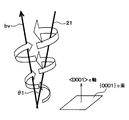
- FIG. 3 is a schematic diagram showing threading dislocations.
- FIG. 4 is a diagram showing the relationship between the angle formed between the Burgers vector of threading dislocation and the dislocation line, and the lifetime of the MOS capacitor, and
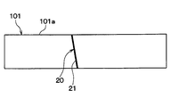
- FIG. 5 is a cross-sectional view of a SiC single crystal wafer in another embodiment.
- SiC single crystal epitaxial wafer 1 has SiC single crystal substrate 2 and SiC epitaxial growth layer 3 formed by epitaxial growth on the surface of SiC single crystal substrate 2.
- the SiC single crystal epitaxial wafer 1 is also referred to as a wafer 1
- the SiC single crystal substrate 2 is also referred to as a single crystal substrate 2
- the SiC epitaxial growth layer 3 is also referred to as an epi layer 3.
- the crystal polymorph of the SiC single crystal constituting the single crystal substrate 2 and the epi layer 3 is 4H.
- the off angle in the ⁇ 11-20> direction with respect to the ⁇ 0001 ⁇ plane on the surface 1a of the wafer 1 (that is, the surface 3a of the epi layer 3) is about 4 °.
- the conductivity type of the epi layer 3 is n-type.
- the SiC single crystal may be other crystal polymorphs such as 6H and 3C.
- the surface 1a of the wafer 1 only needs to have an off angle within 10 ° in the ⁇ 11-20> direction with respect to the ⁇ 0001 ⁇ plane.
- a wafer having a diameter of 100 mm or more or about 150 mm or more can be used.
- the wafer 1 has a micropipe density of less than 1 / cm 2 , a threading edge dislocation density of less than 3000 / cm 2 , a stacking fault density of less than 0.1 / cm 2 , and an inclusion density of 1 / cm 2. Preferably it is less than 3 .
- MOS capacitor 10 is an electronic device having a MOS structure.
- MOS capacitor 10 includes a single crystal substrate 2, an epi layer 3 as an n-type drift layer formed on the surface of SiC single crystal substrate 2, an oxide film 4 formed on surface 3a of epi layer 3, A first electrode 5 formed on the surface of oxide film 4 and a second electrode 6 formed on the back surface of SiC single crystal substrate 2 are provided.
- an oxide film 4 is formed on the surface 1 a of the wafer 1 shown in FIG. 1, a first electrode 5 is formed on the surface of the oxide film 4, and a second electrode is formed on the back surface of the single crystal substrate 2.
- the wafer 1 is manufactured by dicing to a desired size.
- Single crystal substrate 2 and epi layer 3 of wafer 1 correspond to single crystal substrate 2 and epi layer 3 of MOS capacitor 10.
- the “substrate” may refer to the state of the wafer before dicing, and may refer to the state after dicing the wafer.
- the single crystal substrate 2 and the epi layer 3 of the wafer 1 and the single crystal substrate 2 and the epi layer 3 of the MOS capacitor 10 correspond to the SiC single crystal of the present invention.
- threading dislocations 20 exist in the wafer 1, the single crystal substrate 2 of the MOS capacitor 10, and the epitaxial layer 3.
- the threading dislocation 20 is a crystal defect in which the atomic plane is arranged in a spiral around the dislocation line 21.
- This threading dislocation 20 is a dislocation in which the dislocation line 21 penetrates the c-plane of the SiC single crystal and the Burgers vector has at least a component in the c-axis direction.
- the c-plane is the ⁇ 0001 ⁇ plane and the c-axis is the ⁇ 0001> axis.
- the Burgers vector having at least a component in the c-axis direction includes a case where the Burgers vector has only a component in the c-axis direction and a case where the Burgers vector has a component in the c-axis direction and a component in another axis direction. It is.
- the case of bv a + c
- bv m + c
- bv represents a Burgers vector
- a a vector in the 1/3 ⁇ 11-20> direction
- c represents a vector in the ⁇ 0001> direction
- m represents a vector in the ⁇ 1-100> direction.
- the threading dislocation 20 is a dislocation in which the direction of the Burgers vector bv and the direction of the dislocation line 21 are shifted as shown in FIG.
- the strain increases as the angle ⁇ 1 formed by the Burgers vector bv and the direction of the dislocation line 21 increases.
- the range which this angle (theta) 1 can take is larger than 0 degree, and smaller than 90 degree (0 degree ⁇ (theta) 1 ⁇ 90 degree).
- the single crystal substrate 2 and the epi layer 3 have an angle ⁇ 1 between the Burgers vector bv and the direction of the dislocation line among the threading dislocations 20 larger than 0 ° and within 40 ° (0 ° ⁇
- the density of threading dislocations 20 satisfying ⁇ 1 ⁇ 40 ° is set to 300 pieces / cm 2 or less, and the density of threading dislocations 20 having an angle ⁇ 1 larger than 40 ° ( ⁇ 1> 40 °) is set to 30 pieces / cm 2 or less. ing.
- the density of threading dislocations 20 having an angle ⁇ 1 within 20 ° (0 ° ⁇ 1 ⁇ 20 °) is 300 pieces / cm 2 or less, and the angle ⁇ 1 is 20 °.
- the density of threading dislocations 20 larger than ( ⁇ 1> 20 °) is 30 pieces / cm 2 or less.
- the density of threading dislocations 20 having an angle ⁇ 1 within 7 ° (0 ° ⁇ 1 ⁇ 7 °) is 300 pieces / cm 2 or less, and the angle ⁇ 1 is 7
- the density of threading dislocations 20 larger than ° ( ⁇ 1> 7 °) is 30 pieces / cm 2 or less.
- the angle ⁇ 1 larger than 0 ° and within 40 ° means that the angle ⁇ 1 is larger than 0 ° and within 40 °, and is not limited to the case where the angle ⁇ 1 has a uniform size. The case where it is uniform is also included. The same applies to the angle ⁇ 1 within 20 ° and within 7 °.
- Burgers vector bv is obtained by the LACBED method (Large-angle convergent-beam-electron-diffraction). For example, when an electron beam is defocused and the sample is irradiated, the HOLZ line is split by distortion around the dislocation. Therefore, the split HOLZ line is indexed by simulation. It is possible to analyze the Burgers vector bv of threading dislocation 20 from the index of HOLZ line and the number of divisions.
- the direction of the dislocation line 21 is determined by a 3D (three-dimensional) observation method using a TEM (transmission electron microscope).
- TEM transmission electron microscope
- the dislocation inclination in the direction perpendicular to the electron beam incident direction can be evaluated, but the parallel inclination cannot be evaluated. That is, the dislocation inclination in the plane parallel to the electron beam incident direction cannot be evaluated. Therefore, the tilt in the direction parallel to the predetermined incident direction is evaluated by tilting the incident electron beam direction or the sample.
- the tilt angle in the [11-20] direction from the ⁇ 0001> axis can be observed.
- the ⁇ 0001> axis direction is determined from the electron diffraction image.
- the electron beam irradiation direction is rotated symmetrically about the ⁇ 0001> axis. This changes the slope of the observed dislocation.
- the inclination in the [1-100] direction is calculated from the amount of change.
- the direction of the dislocation line 21 can be obtained by using a photoluminescence device (3DPL) having a confocal function or a Raman spectroscopic device (3D Raman) having a confocal function.
- 3DPL photoluminescence device
- 3D Raman Raman spectroscopic device
- the angle formed by the Burgers vector bv and the dislocation line 21 is obtained by a calculation method for obtaining the angle formed by two vectors in the space figure.
- the density of threading dislocations 20 can be obtained by counting the number of threading dislocations 20 existing per 1 cm 2 on a predetermined face of the SiC single crystal.
- the epitaxial layer 3 is etched using a molten salt containing KOH, and the number of threading dislocations 20 in which substantially hexagonal etch pits are observed is counted using a TEM or an optical microscope.
- a surface to be observed a surface inclined from the c-plane and having an inclination angle of 10 ° or less is used.
- the area to be observed is a 1 cm ⁇ 1 cm area.
- the region to be observed may be a region having a size of 1 cm ⁇ 1 cm or more or less than a size of 1 cm ⁇ 1 cm.
- the observation region is preferably a region having a size of 1 cm ⁇ 1 cm or more.
- FIG. 4 shows the relationship between the lifetime of the MOS capacitor 10 and the angle ⁇ 1 formed by the Burgers vector bv of the threading dislocation 20 existing in the single crystal substrate 2 and the epitaxial layer 3 and the dislocation line 21.
- the experimental results examined by the person are shown.
- a wafer 1 having a predetermined density with a threading dislocation 20 having an angle ⁇ 1 of a predetermined size or less is used.
- the density of threading dislocations exceeding the angle of each point of the wafers 1 at points P1, P2, and P3 was 30 pieces / cm 2 or less.
- the wafer 1 at the point P3 has a density of threading dislocations 20 larger than the angle of the point P3 of 30 pieces / cm 2 or less.
- the approximate curve TL1 for the points P1, P2, and P3 in FIG. 4 is obtained by approximating each point with an exponential function by the least square method.
- the Burgers vector bv of threading dislocation 20 was a + c.
- the Burgers vector bv of threading dislocation 20 was m + c.
- the wafer 1 used was manufactured by the manufacturing method described in Japanese Patent No. 3745668.
- the used wafer 1 has a surface 1a with an off angle of about 4 ° set in the ⁇ 11-20> direction with respect to the ⁇ 0001 ⁇ plane. Further, the threading dislocations 20 whose density was measured reached the surface 1a.
- the threading dislocations 20 having an angle ⁇ 1 larger than 0 ° and within 40 ° are suppressed to 300 pieces / cm 2 or less. It was found that the threading dislocations 20 having an angle ⁇ 1 larger than 40 ° should be suppressed to 30 pieces / cm 2 or less.
- the number of threading dislocations 20 in which the angle ⁇ 1 is greater than 0 ° and within 20 ° is suppressed to 300 pieces / cm 2 or less, and the angle ⁇ 1 It was found that the threading dislocations 20 having a diameter greater than 20 ° should be suppressed to 30 pieces / cm 2 or less.
- the number of threading dislocations 20 in which the angle ⁇ 1 is greater than 0 ° and within 7 ° is suppressed to 300 pieces / cm 2 or less, and the angle ⁇ 1 It has been found that the number of threading dislocations 20 greater than 7 ° may be suppressed to 30 pieces / cm 2 or less.
- FIG. 4 shows an experimental result in the case where the threading dislocation angle ⁇ 1 existing in the wafer 1 is equal to or smaller than a specific size. From this experimental result, even if the angle ⁇ 1 is not uniform, If the angle ⁇ 1 is smaller than 40 °, it can be estimated that a high-quality device having a lifetime of 2000 seconds or more can be manufactured.
- the angle ⁇ 1 formed by the Burgers vector bv and the direction of the dislocation line 21 among the threading dislocations 20 existing in the single crystal substrate 2 and the epi layer 3 is larger than 0 ° 40.
- density of ° within the is threading dislocations 20 is 300 / cm 2 or less, is the density of a large threading dislocation 20 of 30 / cm 2 or less than the angle ⁇ 1 is 40 °.
- the density of threading dislocations 20 having an angle ⁇ 1 within 20 ° is preferably 300 pieces / cm 2 or less, and the density of threading dislocations 20 having an angle ⁇ 1 larger than 20 ° is 30 pieces. / Cm 2 or less.
- the density of threading dislocations 20 having an angle ⁇ 1 within 7 ° is 300 pieces / cm 2 or less, and the density of threading dislocations 20 having an angle ⁇ 1 larger than 7 ° is 30. Pieces / cm 2 or less.
- the density of threading dislocations with large strain is reduced. Therefore, the lifetime of the MOS capacitor 10 can be extended by manufacturing the MOS capacitor 10 using the wafer 1 of the present embodiment.
- the angle ⁇ 1 formed by the Burgers vector bv and the direction of the dislocation line 21 among the threading dislocations 20 existing in the single crystal substrate 2 and the epi layer 3 is larger than 0 ° and within 40 °.
- the density of certain threading dislocations 20 is 300 pieces / cm 2 or less, and the density of threading dislocations 20 having an angle ⁇ 1 larger than 40 ° is 30 pieces / cm 2 or less, preferably the angle ⁇ 1 is within 20 °.
- the density of threading dislocations 20 is 300 pieces / cm 2 or less, and the density of threading dislocations 20 having an angle ⁇ 1 larger than 20 ° is 30 pieces / cm 2 or less. More preferably, the angle ⁇ 1 is 7 density of ° within the is threading dislocations 20 is 300 / cm 2 or less, the density of large threading dislocation 20 than the angle ⁇ 1 is 7 ° is 30 / cm 2 or less.
- the single crystal substrate 2 and the epi layer 3 constituting the MOS capacitor 10 have a low density of threading dislocations with a large strain. For this reason, the lifetime of the MOS capacitor 10 can be extended as compared with the case where the density of threading dislocations with large strain is high. That is, the device characteristics of the electronic device can be improved.
- the surface 3a of the epitaxial layer 3 of the wafer 1 and the MOS capacitor 10 has an off angle set within 10 ° in the ⁇ 11-20> direction with respect to the ⁇ 0001 ⁇ plane.
- the angle ⁇ 1 and the density of the threading dislocations 20 existing so as to reach This is because when the threading dislocations 20 having a large strain are present in the vicinity of the surface 3a of the epi layer 3, it is considered that the influence on the device characteristics is particularly large.
- the threading dislocation 20 has a bad influence on the device characteristics not only when the threading dislocation 20 having a large strain is present in the vicinity of the surface 3a of the epi layer 3 but also when the threading dislocation 20 is present in a portion other than the vicinity of the surface 3a of the epi layer 3. It is thought that it exerts. Therefore, the threading dislocations 20 that specify the angle ⁇ 1 and the density are not limited to those existing in the epi layer 3 so as to reach the surface 3a.
- the wafer 1 of the present embodiment is manufactured by the manufacturing method described in Japanese Patent No. 3745668, but may be manufactured by another manufacturing method.
- the MOS capacitor 10 is cited as an example of an electronic device manufactured using a SiC single crystal, and the lifetime of the MOS capacitor 10 is examined. It is thought that the same result is obtained.
- Other electronic devices include electronic devices having a MOS structure other than MOS capacitors, and electronic devices having a diode. Similar to the MOS capacitor 10, the electronic device having the MOS structure has a structure in which the first electrode 5 is formed on the SiC single crystal through the oxide film 4.
- an electronic device having a MOS structure includes a MOSFET having the first electrode 5 as a gate electrode.
- Examples of the electronic device having a diode include a Schottky diode and a PN diode.
- a PN diode can be configured by forming a p-type layer in the surface layer portion of the epi layer 3 and bringing the first electrode 5 into ohmic contact with the p-type layer.
- an electronic device is manufactured using the SiC single crystal epitaxial wafer 1, but an electronic device may be manufactured using the SiC single crystal wafer 101 shown in FIG.
- This SiC single crystal wafer 101 is obtained by forming a SiC single crystal into a substrate and does not have an epitaxial growth layer.
- the SiC single crystal wafer 101 corresponds to the single crystal substrate 2 of the wafer 1 of the first embodiment and the epi layer 3 constituted only by the single crystal substrate 2.
- This SiC single crystal wafer 101 has a low density of threading dislocations with a large strain, like the single crystal substrate 2 of the wafer 1 of the first embodiment. For this reason, the lifetime of an electronic device can be lengthened similarly to 1st Embodiment by manufacturing an electronic device using the SiC single crystal wafer 101.
- the surface 101a has an off angle of 10 ° or less in the ⁇ 11-20> direction with respect to the ⁇ 0001 ⁇ plane, and the threading dislocation 20 reaching this surface 101a. Is preferably specified in the same manner as in the first embodiment.
- the electronic device manufactured in this case is not limited to a structure having a SiC single crystal substrate and a SiC epitaxial growth layer, but may have a structure having an SiC single crystal substrate but no epitaxial growth layer.
- the epi layer 3 is not formed, and the single crystal substrate 2 constitutes a portion corresponding to the epi layer 3. Examples include structures.
- the surface of single crystal substrate 2 corresponds to surface 101 a of SiC single crystal wafer 101.
Landscapes
- Chemical & Material Sciences (AREA)
- Crystallography & Structural Chemistry (AREA)
- Inorganic Chemistry (AREA)
- Engineering & Computer Science (AREA)
- Materials Engineering (AREA)
- Metallurgy (AREA)
- Organic Chemistry (AREA)
- Crystals, And After-Treatments Of Crystals (AREA)
- Physical Vapour Deposition (AREA)
- Chemical Vapour Deposition (AREA)
Abstract
Description
本実施形態では、SiC単結晶エピタキシャルウェハと、このウェハを用いて製造されるMOSキャパシタについて説明する。
本開示は上記した実施形態に限定されるものではなく、下記のように、本開示の主旨を逸脱しない範囲内において適宜変更が可能である。
Claims (13)
- 転位線(21)がc面を貫通するとともに、バーガースベクトル(bv)が少なくともc軸方向の成分を有する貫通転位(20)が存在する炭化珪素単結晶(2、3)であって、
前記貫通転位のうち、前記バーガースベクトルと前記転位線の向きとのなす角度(θ1)が0°より大きく40°以内である貫通転位の密度が300個/cm2以下とされ、前記角度が40°よりも大きな前記貫通転位の密度が30個/cm2以下とされている炭化珪素単結晶。 - 前記角度が20°以内である前記貫通転位の密度が300個/cm2以下とされ、前記角度が20°よりも大きな前記貫通転位の密度が30個/cm2以下とされている請求項1に記載の炭化珪素単結晶。
- 前記角度が7°以内である前記貫通転位の密度が300個/cm2以下とされ、前記角度が7°よりも大きな前記貫通転位の密度が30個/cm2以下とされている請求項1に記載の炭化珪素単結晶。
- 転位線(21)がc面を貫通するとともに、バーガースベクトル(bv)が少なくともc軸方向の成分を有する貫通転位(20)が存在する炭化珪素単結晶ウェハ(101)であって、
前記貫通転位のうち、前記バーガースベクトルと前記転位線の向きとのなす角度(θ1)が0°より大きく40°以内である貫通転位の密度が300個/cm2以下とされ、前記角度が40°よりも大きな前記貫通転位の密度が30個/cm2以下とされている炭化珪素単結晶ウェハ。 - 前記角度が20°以内である前記貫通転位の密度が300個/cm2以下とされ、前記角度が20°よりも大きな前記貫通転位の密度が30個/cm2以下とされている請求項4に記載の炭化珪素単結晶ウェハ。
- 前記角度が7°以内である前記貫通転位の密度が300個/cm2以下とされ、前記角度が7°よりも大きな前記貫通転位の密度が30個/cm2以下とされている請求項4に記載の炭化珪素単結晶ウェハ。
- 炭化珪素単結晶基板(2)と、
前記炭化珪素単結晶基板上に形成されたエピタキシャル成長層(3)とを備え、
前記炭化珪素単結晶基板および前記エピタキシャル成長層は、転位線(21)がc面を貫通するとともに、バーガースベクトル(bv)が少なくともc軸方向の成分を有する貫通転位(20)が存在し、
前記貫通転位のうち、前記バーガースベクトルと前記転位線の向きとのなす角度(θ1)が0°より大きく40°以内である貫通転位の密度が300個/cm2以下とされ、前記角度が40°よりも大きな前記貫通転位の密度が30個/cm2以下とされている炭化珪素単結晶エピタキシャルウェハ。 - 前記角度が20°以内である前記貫通転位の密度が300個/cm2以下とされ、前記角度が20°よりも大きな前記貫通転位の密度が30個/cm2以下とされている請求項7に記載の炭化珪素単結晶エピタキシャルウェハ。
- 前記角度が7°以内である前記貫通転位の密度が300個/cm2以下とされ、前記角度が7°よりも大きな前記貫通転位の密度が30個/cm2以下とされている請求項7に記載の炭化珪素単結晶エピタキシャルウェハ。
- 転位線(21)がc面を貫通するとともに、バーガースベクトル(bv)が少なくともc軸方向の成分を有する貫通転位(20)が存在する炭化珪素単結晶基板(2)を備え、
前記炭化珪素単結晶基板は、前記貫通転位のうち、前記バーガースベクトルと前記転位線の向きとのなす角度(θ1)が0°より大きく40°以内である貫通転位の密度が300個/cm2以下とされ、前記角度が40°よりも大きな前記貫通転位の密度が30個/cm2以下とされている電子デバイス。 - 炭化珪素単結晶基板(2)と、
前記炭化珪素単結晶基板上に形成されたエピタキシャル成長層(3)とを備え、
前記炭化珪素単結晶基板および前記エピタキシャル成長層は、転位線(21)がc面を貫通するとともに、バーガースベクトル(bv)が少なくともc軸方向の成分を有する貫通転位(20)が存在し、前記貫通転位のうち前記バーガースベクトルと前記転位線の向きとのなす角度(θ1)が0°より大きく40°以内である貫通転位の密度が300個/cm2以下とされ、前記角度が40°よりも大きな前記貫通転位の密度が30個/cm2以下とされている電子デバイス。 - 前記角度が20°以内である前記貫通転位の密度が300個/cm2以下とされ、前記角度が20°よりも大きな前記貫通転位の密度が30個/cm2以下とされている請求項10または11に記載の電子デバイス。
- 前記角度が7°以内である前記貫通転位の密度が300個/cm2以下とされ、前記角度が7°よりも大きな前記貫通転位の密度が30個/cm2以下とされている請求項10または11に記載の電子デバイス。
Priority Applications (4)
| Application Number | Priority Date | Filing Date | Title |
|---|---|---|---|
| US15/748,274 US10181517B2 (en) | 2015-08-31 | 2016-08-25 | Silicon carbide single crystal, silicon carbide single crystal wafer, silicon carbide single crystal epitaxial wafer, and electronic device |
| CN201680049110.4A CN108026661B (zh) | 2015-08-31 | 2016-08-25 | 碳化硅单晶、碳化硅单晶晶片、碳化硅单晶外延晶片、电子器件 |
| DE112016003919.0T DE112016003919B4 (de) | 2015-08-31 | 2016-08-25 | Verwendung eines siliciumcarbideinkristallwafers zur herstellung einer elektronischen vorrichtung |
| KR1020187008839A KR102132209B1 (ko) | 2015-08-31 | 2016-08-25 | 탄화 규소 단결정, 탄화 규소 단결정 웨이퍼, 탄화 규소 단결정 에피택셜 웨이퍼, 전자 디바이스 |
Applications Claiming Priority (2)
| Application Number | Priority Date | Filing Date | Title |
|---|---|---|---|
| JP2015-170814 | 2015-08-31 | ||
| JP2015170814A JP6597065B2 (ja) | 2015-08-31 | 2015-08-31 | 炭化珪素単結晶、炭化珪素単結晶ウェハ、炭化珪素単結晶エピタキシャルウェハ、電子デバイス |
Publications (1)
| Publication Number | Publication Date |
|---|---|
| WO2017038591A1 true WO2017038591A1 (ja) | 2017-03-09 |
Family
ID=58188780
Family Applications (1)
| Application Number | Title | Priority Date | Filing Date |
|---|---|---|---|
| PCT/JP2016/074724 Ceased WO2017038591A1 (ja) | 2015-08-31 | 2016-08-25 | 炭化珪素単結晶、炭化珪素単結晶ウェハ、炭化珪素単結晶エピタキシャルウェハ、電子デバイス |
Country Status (6)
| Country | Link |
|---|---|
| US (1) | US10181517B2 (ja) |
| JP (1) | JP6597065B2 (ja) |
| KR (1) | KR102132209B1 (ja) |
| CN (1) | CN108026661B (ja) |
| DE (1) | DE112016003919B4 (ja) |
| WO (1) | WO2017038591A1 (ja) |
Families Citing this family (4)
| Publication number | Priority date | Publication date | Assignee | Title |
|---|---|---|---|---|
| JP7209955B2 (ja) | 2018-08-30 | 2023-01-23 | 国立研究開発法人産業技術総合研究所 | n型4H-SiC単結晶基板およびn型4H-SiC単結晶基板の製造方法 |
| KR102192518B1 (ko) | 2020-07-14 | 2020-12-17 | 에스케이씨 주식회사 | 웨이퍼 및 웨이퍼의 제조방법 |
| JP7260039B1 (ja) * | 2022-06-02 | 2023-04-18 | 株式会社レゾナック | SiC単結晶基板 |
| JP2025030917A (ja) * | 2023-08-24 | 2025-03-07 | 株式会社レゾナック | SiC基板及びSiCエピタキシャルウェハ |
Citations (4)
| Publication number | Priority date | Publication date | Assignee | Title |
|---|---|---|---|---|
| JP3745668B2 (ja) * | 2001-10-12 | 2006-02-15 | 株式会社豊田中央研究所 | SiC単結晶の製造方法並びにSiC種結晶の製造方法 |
| JP2010184833A (ja) * | 2009-02-12 | 2010-08-26 | Denso Corp | 炭化珪素単結晶基板および炭化珪素単結晶エピタキシャルウェハ |
| JP2014159351A (ja) * | 2013-02-20 | 2014-09-04 | Denso Corp | 炭化珪素単結晶および炭化珪素単結晶の製造方法 |
| JP2014227319A (ja) * | 2013-05-23 | 2014-12-08 | 株式会社豊田中央研究所 | SiC単結晶及びその製造方法 |
Family Cites Families (7)
| Publication number | Priority date | Publication date | Assignee | Title |
|---|---|---|---|---|
| DE10247017B4 (de) | 2001-10-12 | 2009-06-10 | Denso Corp., Kariya-shi | SiC-Einkristall, Verfahren zur Herstellung eines SiC-Einkristalls, SiC-Wafer mit einem Epitaxiefilm und Verfahren zur Herstellung eines SiC-Wafers, der einen Epitaxiefilm aufweist |
| US7314520B2 (en) | 2004-10-04 | 2008-01-01 | Cree, Inc. | Low 1c screw dislocation 3 inch silicon carbide wafer |
| JP4758492B2 (ja) * | 2009-03-24 | 2011-08-31 | トヨタ自動車株式会社 | 単結晶の欠陥密度測定方法 |
| JP5696630B2 (ja) | 2011-09-21 | 2015-04-08 | 住友電気工業株式会社 | 炭化珪素基板およびその製造方法 |
| JP5931825B2 (ja) * | 2013-09-20 | 2016-06-08 | 新日鉄住金マテリアルズ株式会社 | 炭化珪素単結晶インゴットの製造方法 |
| JP6467775B2 (ja) | 2014-03-10 | 2019-02-13 | 富士通株式会社 | 部品内蔵基板の製造方法 |
| KR102160863B1 (ko) * | 2014-09-30 | 2020-09-28 | 쇼와 덴코 가부시키가이샤 | 탄화규소 단결정 웨이퍼 |
-
2015
- 2015-08-31 JP JP2015170814A patent/JP6597065B2/ja active Active
-
2016
- 2016-08-25 KR KR1020187008839A patent/KR102132209B1/ko active Active
- 2016-08-25 US US15/748,274 patent/US10181517B2/en active Active
- 2016-08-25 DE DE112016003919.0T patent/DE112016003919B4/de active Active
- 2016-08-25 WO PCT/JP2016/074724 patent/WO2017038591A1/ja not_active Ceased
- 2016-08-25 CN CN201680049110.4A patent/CN108026661B/zh active Active
Patent Citations (4)
| Publication number | Priority date | Publication date | Assignee | Title |
|---|---|---|---|---|
| JP3745668B2 (ja) * | 2001-10-12 | 2006-02-15 | 株式会社豊田中央研究所 | SiC単結晶の製造方法並びにSiC種結晶の製造方法 |
| JP2010184833A (ja) * | 2009-02-12 | 2010-08-26 | Denso Corp | 炭化珪素単結晶基板および炭化珪素単結晶エピタキシャルウェハ |
| JP2014159351A (ja) * | 2013-02-20 | 2014-09-04 | Denso Corp | 炭化珪素単結晶および炭化珪素単結晶の製造方法 |
| JP2014227319A (ja) * | 2013-05-23 | 2014-12-08 | 株式会社豊田中央研究所 | SiC単結晶及びその製造方法 |
Also Published As
| Publication number | Publication date |
|---|---|
| KR20180044999A (ko) | 2018-05-03 |
| CN108026661B (zh) | 2020-11-10 |
| DE112016003919T5 (de) | 2018-05-09 |
| US10181517B2 (en) | 2019-01-15 |
| CN108026661A (zh) | 2018-05-11 |
| JP6597065B2 (ja) | 2019-10-30 |
| US20180219069A1 (en) | 2018-08-02 |
| DE112016003919T8 (de) | 2018-07-19 |
| KR102132209B1 (ko) | 2020-07-10 |
| JP2017048068A (ja) | 2017-03-09 |
| DE112016003919B4 (de) | 2025-11-13 |
Similar Documents
| Publication | Publication Date | Title |
|---|---|---|
| JP5000424B2 (ja) | 炭化珪素単結晶ウェハの欠陥検出方法、及び炭化珪素半導体素子の製造方法 | |
| JP2023025002A (ja) | ミスカット基板を用いた高パワーの窒化ガリウムエレクトロニクス | |
| US8860040B2 (en) | High voltage power semiconductor devices on SiC | |
| US20220223482A1 (en) | EVALUATION METHOD AND MANUFACTURING METHOD OF SiC EPITAXIAL WAFER | |
| JP6597065B2 (ja) | 炭化珪素単結晶、炭化珪素単結晶ウェハ、炭化珪素単結晶エピタキシャルウェハ、電子デバイス | |
| Besendörfer et al. | Vertical breakdown of GaN on Si due to V-pits | |
| KR20140022074A (ko) | SiC 단결정, SiC 웨이퍼 및 반도체 디바이스 | |
| Ha et al. | Dislocation nucleation in 4H silicon carbide epitaxy | |
| US11249027B2 (en) | SiC substrate evaluation method and method for manufacturing SiC epitaxtal wafer | |
| Berechman et al. | Electrical characterization of 4H–SiC avalanche photodiodes containing threading edge and screw dislocations | |
| JP2016166112A (ja) | 半導体基板及び半導体装置 | |
| US10985079B2 (en) | Method of manufacturing SiC epitaxial wafer | |
| Jnawali et al. | Room-temperature quantum transport signatures in graphene/LaAlO3/SrTiO3 heterostructures | |
| JP2020126985A (ja) | SiCエピタキシャルウェハ及びその製造方法 | |
| El Hageali et al. | Nondestructive microstructural investigation of defects in 4H-SiC epilayers using a multiscale luminescence analysis approach | |
| Kim et al. | Microscopic-scale defect analysis on β-Ga2O3 through microscopy | |
| CN105074059B (zh) | 碳化硅单晶以及碳化硅单晶的制造方法 | |
| JP6061017B1 (ja) | 半導体エピタキシャルウェーハの汚染評価方法およびそれを用いたエピタキシャル成長装置の汚染評価方法 | |
| Xu et al. | Breakdown characteristics analysis of kV-class vertical GaN PIN rectifiers by wafer-level sub-bandgap photoluminescence mapping | |
| Berechman et al. | Trapezoid defect in 4H–SiC epilayers | |
| JP2020063186A (ja) | SiCエピタキシャルウェハ | |
| Winchester et al. | Electronic properties of extended surface defects in homoepitaxial GaN diodes | |
| JP5558268B2 (ja) | 半導体単結晶基板の欠陥観察方法 | |
| Kitabatake et al. | The integrated evaluation platform for SiC wafers and epitaxial films | |
| JP2023054875A (ja) | ウェーハ及び半導体装置 |
Legal Events
| Date | Code | Title | Description |
|---|---|---|---|
| 121 | Ep: the epo has been informed by wipo that ep was designated in this application |
Ref document number: 16841623 Country of ref document: EP Kind code of ref document: A1 |
|
| WWE | Wipo information: entry into national phase |
Ref document number: 15748274 Country of ref document: US |
|
| WWE | Wipo information: entry into national phase |
Ref document number: 112016003919 Country of ref document: DE |
|
| ENP | Entry into the national phase |
Ref document number: 20187008839 Country of ref document: KR Kind code of ref document: A |
|
| 122 | Ep: pct application non-entry in european phase |
Ref document number: 16841623 Country of ref document: EP Kind code of ref document: A1 |
|
| WWG | Wipo information: grant in national office |
Ref document number: 112016003919 Country of ref document: DE |