WO2017038020A1 - カラーフィルタ及びこれを用いた液晶ディスプレイ - Google Patents
カラーフィルタ及びこれを用いた液晶ディスプレイ Download PDFInfo
- Publication number
- WO2017038020A1 WO2017038020A1 PCT/JP2016/003652 JP2016003652W WO2017038020A1 WO 2017038020 A1 WO2017038020 A1 WO 2017038020A1 JP 2016003652 W JP2016003652 W JP 2016003652W WO 2017038020 A1 WO2017038020 A1 WO 2017038020A1
- Authority
- WO
- WIPO (PCT)
- Prior art keywords
- color filter
- liquid crystal
- film
- conductive alloy
- alloy film
- Prior art date
- Legal status (The legal status is an assumption and is not a legal conclusion. Google has not performed a legal analysis and makes no representation as to the accuracy of the status listed.)
- Ceased
Links
Images





Classifications
-
- G—PHYSICS
- G06—COMPUTING OR CALCULATING; COUNTING
- G06F—ELECTRIC DIGITAL DATA PROCESSING
- G06F3/00—Input arrangements for transferring data to be processed into a form capable of being handled by the computer; Output arrangements for transferring data from processing unit to output unit, e.g. interface arrangements
- G06F3/01—Input arrangements or combined input and output arrangements for interaction between user and computer
- G06F3/03—Arrangements for converting the position or the displacement of a member into a coded form
- G06F3/041—Digitisers, e.g. for touch screens or touch pads, characterised by the transducing means
- G06F3/044—Digitisers, e.g. for touch screens or touch pads, characterised by the transducing means by capacitive means
- G06F3/0446—Digitisers, e.g. for touch screens or touch pads, characterised by the transducing means by capacitive means using a grid-like structure of electrodes in at least two directions, e.g. using row and column electrodes
-
- G—PHYSICS
- G02—OPTICS
- G02B—OPTICAL ELEMENTS, SYSTEMS OR APPARATUS
- G02B5/00—Optical elements other than lenses
- G02B5/20—Filters
-
- G—PHYSICS
- G02—OPTICS
- G02F—OPTICAL DEVICES OR ARRANGEMENTS FOR THE CONTROL OF LIGHT BY MODIFICATION OF THE OPTICAL PROPERTIES OF THE MEDIA OF THE ELEMENTS INVOLVED THEREIN; NON-LINEAR OPTICS; FREQUENCY-CHANGING OF LIGHT; OPTICAL LOGIC ELEMENTS; OPTICAL ANALOGUE/DIGITAL CONVERTERS
- G02F1/00—Devices or arrangements for the control of the intensity, colour, phase, polarisation or direction of light arriving from an independent light source, e.g. switching, gating or modulating; Non-linear optics
- G02F1/01—Devices or arrangements for the control of the intensity, colour, phase, polarisation or direction of light arriving from an independent light source, e.g. switching, gating or modulating; Non-linear optics for the control of the intensity, phase, polarisation or colour
- G02F1/13—Devices or arrangements for the control of the intensity, colour, phase, polarisation or direction of light arriving from an independent light source, e.g. switching, gating or modulating; Non-linear optics for the control of the intensity, phase, polarisation or colour based on liquid crystals, e.g. single liquid crystal display cells
- G02F1/133—Constructional arrangements; Operation of liquid crystal cells; Circuit arrangements
- G02F1/1333—Constructional arrangements; Manufacturing methods
-
- G—PHYSICS
- G02—OPTICS
- G02F—OPTICAL DEVICES OR ARRANGEMENTS FOR THE CONTROL OF LIGHT BY MODIFICATION OF THE OPTICAL PROPERTIES OF THE MEDIA OF THE ELEMENTS INVOLVED THEREIN; NON-LINEAR OPTICS; FREQUENCY-CHANGING OF LIGHT; OPTICAL LOGIC ELEMENTS; OPTICAL ANALOGUE/DIGITAL CONVERTERS
- G02F1/00—Devices or arrangements for the control of the intensity, colour, phase, polarisation or direction of light arriving from an independent light source, e.g. switching, gating or modulating; Non-linear optics
- G02F1/01—Devices or arrangements for the control of the intensity, colour, phase, polarisation or direction of light arriving from an independent light source, e.g. switching, gating or modulating; Non-linear optics for the control of the intensity, phase, polarisation or colour
- G02F1/13—Devices or arrangements for the control of the intensity, colour, phase, polarisation or direction of light arriving from an independent light source, e.g. switching, gating or modulating; Non-linear optics for the control of the intensity, phase, polarisation or colour based on liquid crystals, e.g. single liquid crystal display cells
- G02F1/133—Constructional arrangements; Operation of liquid crystal cells; Circuit arrangements
- G02F1/1333—Constructional arrangements; Manufacturing methods
- G02F1/1335—Structural association of cells with optical devices, e.g. polarisers or reflectors
-
- G—PHYSICS
- G02—OPTICS
- G02F—OPTICAL DEVICES OR ARRANGEMENTS FOR THE CONTROL OF LIGHT BY MODIFICATION OF THE OPTICAL PROPERTIES OF THE MEDIA OF THE ELEMENTS INVOLVED THEREIN; NON-LINEAR OPTICS; FREQUENCY-CHANGING OF LIGHT; OPTICAL LOGIC ELEMENTS; OPTICAL ANALOGUE/DIGITAL CONVERTERS
- G02F1/00—Devices or arrangements for the control of the intensity, colour, phase, polarisation or direction of light arriving from an independent light source, e.g. switching, gating or modulating; Non-linear optics
- G02F1/01—Devices or arrangements for the control of the intensity, colour, phase, polarisation or direction of light arriving from an independent light source, e.g. switching, gating or modulating; Non-linear optics for the control of the intensity, phase, polarisation or colour
- G02F1/13—Devices or arrangements for the control of the intensity, colour, phase, polarisation or direction of light arriving from an independent light source, e.g. switching, gating or modulating; Non-linear optics for the control of the intensity, phase, polarisation or colour based on liquid crystals, e.g. single liquid crystal display cells
- G02F1/133—Constructional arrangements; Operation of liquid crystal cells; Circuit arrangements
- G02F1/1333—Constructional arrangements; Manufacturing methods
- G02F1/1343—Electrodes
-
- G—PHYSICS
- G06—COMPUTING OR CALCULATING; COUNTING
- G06F—ELECTRIC DIGITAL DATA PROCESSING
- G06F3/00—Input arrangements for transferring data to be processed into a form capable of being handled by the computer; Output arrangements for transferring data from processing unit to output unit, e.g. interface arrangements
- G06F3/01—Input arrangements or combined input and output arrangements for interaction between user and computer
- G06F3/03—Arrangements for converting the position or the displacement of a member into a coded form
- G06F3/041—Digitisers, e.g. for touch screens or touch pads, characterised by the transducing means
Definitions
- the present invention relates to a color filter and a liquid crystal display using the same.
- color liquid crystal display devices have formed a large market as liquid crystal color televisions and liquid crystal display device-integrated notebook personal computers.
- personal digital assistants, car navigation systems, touch panel type liquid crystal displays that use a touch panel as an input / output device for image information, with the touch panel integrated with the liquid crystal display panel, have become popular in the market. It was.
- the capacitive touch panel has a translucent conductive film (translucent electrode) on a single substrate, and has a capacitance formed by contact (touch) with a finger or a pen.
- the position to be contacted is specified by detecting a change in the amount of weak current flowing through the device, and the instructed content is received as an input signal to drive the liquid crystal display device.
- a capacitive touch panel that does not have a movable part has high optical characteristics (transmittance), and is superior in durability and operating temperature characteristics to a resistive touch panel.
- TFT thin film transistor
- An on-cell type has a touch panel function built in between the glass substrate.
- the in-cell type has a concern that the yield may be lowered by incorporating the touch sensor function inside the pixel on the TFT substrate.
- Another problem is that by incorporating a touch sensor in a pixel, the area that can be used for display is reduced and the image quality is deteriorated.
- the on-cell type forms an electrode pattern between the color filter substrate and the polarizing plate, it is easy to ensure the yield. Further, since the area of the effective display area in the pixel is not reduced, there is almost no deterioration in image quality.
- Patent Document 1 describes a method of manufacturing an on-cell capacitive touch panel sensor substrate that has an excellent display quality and that is cheaper than a conventional conductive transparent electrode and that does not impair visibility. For the purpose of providing, it is described that silver particles are used for wiring.
- An object of the present invention is to provide a color filter with a capacitive touch sensing electrode of an electrostatic capacity type that reduces the load of the manufacturing process and has excellent heat resistance and specific resistance, and a liquid crystal display using the same.
- the present invention is a color filter comprising a transparent base material and a conductive alloy film made of an alloy of copper and nickel or an alloy of copper, nickel and titanium on at least one surface of the transparent base material.
- the present invention is a liquid crystal display including the color filter, a liquid crystal layer, and a TFT substrate.
- the present invention it is possible to realize a color filter with a capacitive touch sensing electrode with excellent heat resistance and specific resistance, and a liquid crystal display using the same, by reducing the load of the manufacturing process. .
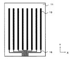
- FIG. 1 is a plan view of a surface of a color filter according to an embodiment on which a colored layer is laminated, excluding a transparent insulating film 15 ′ provided on the forefront.
- FIG. 2 is a plan view of the surface of the color filter according to the embodiment where the colored layer is not laminated, and is a diagram excluding the transparent insulating film 15 provided on the forefront.
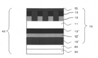
- FIG. 3A is a cross-sectional view showing an example of the configuration of the color filter according to the embodiment, and shows a cross-sectional view along the cutting line AA of the color filter of FIG. FIG.
- FIG. 3B is a cross-sectional view showing an example of the configuration of the color filter according to the embodiment, and shows a cross-sectional view along the cutting line BB of the color filter of FIG.
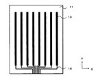
- FIG. 4 is a plan view of a surface on which a colored layer in the color filter according to Example 3 is laminated, and illustrates a diagram excluding the transparent insulating film 15 ′ provided on the foremost surface.
- FIG. 5 is a plan view of a surface of the color filter according to Example 3 on which a colored layer is not stacked, and a diagram excluding the transparent insulating film 15 provided on the forefront.
- FIG. 4 is a plan view of a surface on which a colored layer in the color filter according to Example 3 is laminated, and illustrates a diagram excluding the transparent insulating film 15 ′ provided on the foremost surface.
- FIG. 5 is a plan view of a surface of the color filter according to Example 3 on which a colored layer is not stacked, and a diagram excluding the transparent insulating
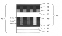
- FIG. 6 is a cross-sectional view showing an example of the configuration of the color filter according to the third embodiment, and shows a cross-sectional view along the cutting line CC of the color filter of FIG.
- FIG. 7 is a plan view of a surface on which a colored layer in the color filter according to Example 4 is stacked, and illustrates a diagram excluding the transparent insulating film 15 ′ provided on the foremost surface.
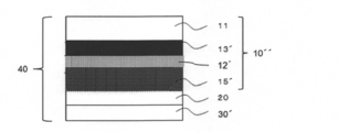
- FIG. 8A is a cross-sectional view illustrating an example of the configuration of the color filter according to the fourth embodiment, and illustrates a cross-sectional view along the cutting line DD of the color filter of FIG.
- FIG. 8B is a cross-sectional view illustrating an example of the configuration of the color filter according to the fourth embodiment, and illustrates a cross-sectional view along the cutting line EE of the color filter of FIG.
- FIG. 1 is a plan view of a surface of a color filter according to an embodiment on which a colored layer is laminated, in which a transparent insulating film 15 ′ provided on the forefront is removed
- FIG. 2 is a color according to the embodiment. It is a top view of the surface in which the colored layer in a filter is not laminated
- 3A is a cross-sectional view taken along the cutting line AA of the color filter of FIG. 1, and FIG. 3B is a cross-sectional view taken along the cutting line BB.
- the color filter 10 includes a transparent substrate 11, conductive alloy films 12 and 12 ′, blackening layers 13 and 13 ′, and a colored layer 14R. , 14G and 14B, transparent insulating layers 15 and 15 ', and FPC (Flexible Printed Circuits) connection electrode wires 16.
- a grid-like blackened layer 13 ′ that partitions a plurality of pixels in the X-axis direction and the Y-axis direction, and in the openings of the blackened layer 13 ′
- Colored layers 14R, 14G and 14B to be formed a plurality of conductive alloy films 12 'formed on a portion extending in the X-axis direction of the blackened layer 13', and a transparent insulating film 15 'covering the outermost surface Is provided.
- the plurality of conductive alloy films 12 ′ extend in the X-axis direction and are arranged at predetermined intervals in the Y-axis direction.
- the transparent substrate 11 opposite to the colored layer forming surface there are a plurality of conductive alloy films 12 extending in the Y-axis direction, and a blackened layer 13 laminated on the conductive alloy film 12. Provided.
- the plurality of conductive alloy films 12 are arranged at predetermined intervals in the X-axis direction.
- the FPC connection electrode wires 16 are provided on both surfaces of the transparent substrate 11, and are connected to the conductive alloy films 12 and 12 '.
- the liquid crystal display 40 having a touch panel function includes the color filter 10 and the liquid crystal layer 20 sequentially stacked on the colored layer forming surface of the color filter 10.
- the TFT substrate 30 is provided.
- the transparent base material 11 a material having a transmittance of 80% or more with respect to visible light can be used, and a material having a transmittance of 95% or more can be preferably used. It may be generally used for liquid crystal display devices, and an inorganic transparent substrate such as glass or a transparent resin substrate such as polycarbonate, polymethyl methacrylate, polyethylene terephthalate, and cyclic olefin copolymer can be used. These may be used alone or in combination of two or more materials. Since the touch panel function according to the present embodiment is a capacitive type, there is no risk of distortion due to external force as in the conventional touch screen system, and the material and thickness can be appropriately selected depending on the specifications of the display panel to be applied. Considering the heat resistance of the glass substrate, the glass substrate is optimal.
- the conductive alloy films 12 and 12 ' are formed of an alloy of copper and nickel or an alloy of copper, nickel and titanium.
- the composition ratio of the conductive alloy film 12 or 12 ′ is not limited as long as the sheet resistance is 0.10 ⁇ / ⁇ or less and the film thickness is 600 nm or less.
- an arbitrary adhesion film may be provided for the purpose of improving the adhesion between the transparent substrate 11 and the conductive alloy film 12.
- the adhesion film include, but are not limited to, a method of obtaining an ITO or SiO 2 film by a sputtering method.
- a sputtering method is usually used as a method for forming the conductive alloy films 12 and 12 '.
- any method that can obtain a film with a uniform film thickness on the transparent substrate 11 such as a CVD method or a vapor deposition method may be used. It is not limited to.
- the blackening layers 13 and 13 ′ are preferably made of, for example, an acrylic resin having a thickness of 0.5 to 3.0 ⁇ m in which a black pigment is dispersed. Particularly, an insulating material having a reflectance of 20% or less is used. There is no limitation.
- the colored layers 14R, 14G, and 14B are layers colored in red, green, and blue, respectively.
- the colored layers 14R, 14G, and 14B are made of an acrylic resin having a thickness of 0.5 to 3.0 ⁇ m in which pigments of respective colors are dispersed.
- spin coating and spinless coating are usually used. Further, a dipping method can be used as a method for forming the blackening layers 13 and 13 'in a lump, but the method is not limited thereto as long as it can be applied on the transparent substrate 11 with a uniform film thickness.
- the transparent insulating layers 15 and 15 ' are formed for the purpose of protecting the colored layers 14R, 14G, and 14B.
- the material can be formed using a known material, for example, an organic material such as a transparent resin having photosensitivity.
- an organic material such as a transparent resin having photosensitivity.
- a UV curable coating composition containing a polymerizable group-containing oligomer, monomer, photopolymerization initiator and other additives can be used.
- a photolithography method is usually used as a method for forming the shapes of the conductive alloy films 12, 12 ', the blackened layers 13, 13', and the colored layers 14R, 14G, 14B.
- the electrode line 16 for FPC connection is formed for the purpose of connecting the conductive alloy films 12 and 12 'to an IC used for controlling the touch panel.
- the material include conductive metal pastes, conductive metal nanowires, thin film metals, and the like, and particularly those that can obtain a low resistance sufficient for conducting the IC and the conductive alloy films 12 and 12 '.
- the formation method is not particularly limited, and examples thereof include wet coating such as gravure offset printing, screen printing, and flexographic printing, and dry coating such as sputtering, vapor deposition, and CVD.
- the conductive alloy film 12 ′ that is the electrode pattern in the X-axis direction and the conductive alloy film 12 that is the electrode pattern in the Y-axis direction are formed through the transparent substrate 11.
- liquid crystal display 40 having a touch panel function can be obtained by bonding the color filter 10 of the present embodiment to the TFT substrate 30 and forming the known liquid crystal layer 20 in the gap.
- a conductive alloy film made of an alloy of copper and nickel or an alloy of copper, nickel and titanium on at least one surface of the transparent substrate, it is excellent in heat resistance and specific resistance.
- a color filter having a capacitive touch sensing electrode can be obtained.
- the electrode since the electrode has excellent heat resistance, a heat-resistant protective film is not required, so that the load on the manufacturing process can be reduced.
- Example 1 As Example 1, a color filter 10 having the configuration shown in FIGS. 1, 2, 3A and 3B was prepared. Further, the color filter 10 and the TFT substrate 30 were bonded together, and a known liquid crystal layer 20 was formed in the gap between them, and a liquid crystal display 40 having a touch panel function was created.
- cleaning was implemented for 30 second with 0.2 mass% sodium hydrogencarbonate aqueous solution.
- heat treatment was performed at 230 ° C. for 30 minutes in a hot air circulation oven to form blackened layers 13 and 13 ′.
- the thickness of the blackening layers 13 and 13 ′ was 1 ⁇ m.
- the conductive alloy film 12 was patterned by a wet etching method by dipping in an etching solution in which 0.2% by mass of sulfuric acid and 0.2% by mass of hydrogen peroxide were mixed.
- a conductive alloy film 12 ′ is formed on the blackened layer 13 ′ by using the same material and method as the conductive alloy film 12, and similarly 0.2 mass% sulfuric acid and 0.2 mass% hydrogen peroxide. Patterning was performed by a wet etching method using an etching solution mixed with water.
- a colored layer 14R, a colored layer 14G, and a colored layer 14B were sequentially formed with a thickness of 2.5 ⁇ m on the surface on which the blackening layer 13 ′ was formed.
- the forming method is that an acrylic resin colored in each color is applied by a spin coating method, and then cured by exposing the light amount of 100 mJ / cm 2 using a high-pressure mercury lamp. A method of developing by applying a shower of 0.2 mass% sodium hydrogen carbonate aqueous solution for 30 seconds was used. After that, as the transparent insulating layers 15 and 15 ', an overcoat agent V-259PA manufactured by Nippon Steel & Sumikin Chemical Co., Ltd.
- Mino Group MP-704GO was formed by gravure offset printing and dried at 130 ° C. for 10 minutes to a thickness of 2 ⁇ m.
- a color filter 10 according to Example 1 was created. Thereafter, the surface of the color filter 10 on which the colored layers 14R, 14G, and 14B are formed and the TFT substrate 30 are bonded together with a sealing material, and a liquid crystal material is injected into the gap to form the liquid crystal layer 20 and has a touch panel function. A liquid crystal display 40 was created.
- Example 2 As Example 2, the color filter 10 having the configuration shown in FIGS. 1, 2, 3A, and 3B was prepared. Further, the color filter 10 and the TFT substrate 30 were bonded together, and a known liquid crystal layer 20 was formed in the gap between them, and a liquid crystal display 40 having a touch panel function was created.
- a black matrix resin in which a black pigment was mixed with an acrylic resin as a blackening layer was applied to both surfaces of the glass by a spin coat method, and dried at 120 ° C. for 2 minutes on a hot plate to dry the coating film. Then, after exposing through the photomask which has a desired opening part with the exposure amount of 100 mJ / cm ⁇ 2 > with a high pressure mercury lamp as a light source, the shower washing
- the thickness of the blackening layers 13 and 13 ′ was 1 ⁇ m.
- the conductive alloy film 12 was patterned by a wet etching method by dipping in an etching solution in which 0.2% by mass of sulfuric acid and 0.2% by mass of hydrogen peroxide were mixed. Thereafter, a conductive alloy film 12 ′ is formed on the blackened layer 13 ′ by using the same material and method as the conductive alloy film 12, and similarly 0.2 mass% sulfuric acid and 0.2 mass% hydrogen peroxide. Patterning was performed by a wet etching method using an etching solution mixed with water.
- a colored layer 14R, a colored layer 14G, and a colored layer 14B were sequentially formed with a thickness of 2.5 ⁇ m on the surface on which the blackening layer 13 ′ was formed.
- the forming method is that an acrylic resin colored in each color is applied by a spin coating method, and then cured by exposing the light amount of 100 mJ / cm 2 using a high-pressure mercury lamp. A method of developing by applying a shower of 0.2 mass% sodium hydrogen carbonate aqueous solution for 30 seconds was used. After that, as the transparent insulating layers 15 and 15 ', an overcoat agent V-259PA manufactured by Nippon Steel & Sumikin Chemical Co., Ltd.
- Mino Group MP-704GO was formed by gravure offset printing and dried at 130 ° C. for 10 minutes to a thickness of 2 ⁇ m.
- a color filter 10 according to Example 2 was created. After that, the surface of the color filter 10 on which the colored layers 14R, 14G, and 14B are formed and the TFT substrate 30 are bonded together with a sealing material, and a liquid crystal material is injected into the gap to form the liquid crystal layer 20, thereby providing a touch panel function.
- the liquid crystal display 40 which has was created.
- Example 3 As Example 3, a color filter 10 ′ having the configuration shown in FIGS. 4 to 6 was prepared. Further, the color filter 10 ′ and the TFT substrate 30 ′ having the capacitive touch sensing electrode were bonded together, and a known liquid crystal layer 20 was formed in the gap, thereby producing a liquid crystal display 40 having a touch panel function. .
- FIG. 4 is a plan view of the surface on which the colored layers in the color filter according to Example 3 are laminated, and is a diagram excluding the transparent insulating film 15 ′ provided on the forefront
- FIG. FIG. 6 is a plan view of a surface of the color filter according to Example 3 on which a colored layer is not laminated, and is a diagram excluding the transparent insulating film 15 provided on the forefront
- FIG. 6 is a configuration of the color filter according to Example 3
- FIG. 5 is a cross-sectional view showing an example of the color filter taken along a cutting line CC of the color filter of FIG. 4.
- the color filter 10 ′ according to Example 3 includes a transparent substrate 11, a conductive alloy film 12, blackening layers 13 and 13 ′, colored layers 14R, 14G, and 14B, transparent insulating layers 15 and 15 ', and an FPC connection electrode line 16. That is, in Example 3, the conductive alloy film 12 ′ on the colored layer forming surface shown in FIG. 1 is omitted.
- the liquid crystal display 40 having a touch panel function according to the third embodiment includes the color filter 10 ′, the liquid crystal layer 20, and a TFT substrate 30 ′ including a capacitive touch sensing electrode. In the liquid crystal display 40 according to the present embodiment, the touch position is detected using the conductive alloy film 12 provided on the color filter 10 ′ and the touch sensing electrode provided on the TFT substrate 30 ′.
- cleaning was implemented for 30 second with 0.2 mass% sodium hydrogencarbonate aqueous solution.
- heat treatment was performed at 230 ° C. for 30 minutes in a hot air circulation oven to form blackened layers 13 and 13 ′.
- the thickness of the blackening layers 13 and 13 ′ was 1 ⁇ m.
- the conductive alloy film 12 was patterned by a wet etching method by dipping in an etching solution in which 0.2% by mass of sulfuric acid and 0.2% by mass of hydrogen peroxide were mixed.
- a colored layer 14R, a colored layer 14G, and a colored layer 14B were sequentially formed with a thickness of 2.5 ⁇ m on the surface on which the blackening layer 13 ′ was formed.
- the forming method is that an acrylic resin colored in each color is applied by a spin coating method, and then cured by exposing the light amount of 100 mJ / cm 2 using a high-pressure mercury lamp. A method of developing by applying a shower of 0.2 mass% sodium hydrogen carbonate aqueous solution for 30 seconds was used. After that, as the transparent insulating layers 15 and 15 ', an overcoat agent V-259PA manufactured by Nippon Steel & Sumikin Chemical Co., Ltd.
- Mino Group MP-704GO was formed by gravure offset printing and dried at 130 ° C. for 10 minutes to a thickness of 2 ⁇ m.
- a color filter 10 'according to Example 3 was created. After that, the surface of the color filter 10 ′ on which the colored layers 14R, 14G, and 14B are formed and the TFT substrate 30 ′ having the capacitive touch sensing electrode are bonded together with a sealing material, and a liquid crystal material is provided in the gap.
- the liquid crystal layer 20 was formed by injecting the liquid crystal to produce a liquid crystal display 40 having a touch panel function.
- the liquid crystal display 40 having the touch panel function according to the third embodiment is connected to the IC and the touch sensing and the liquid crystal driving are confirmed, the conductive alloy film 12 provided on the color filter 10 ′ and the TFT substrate 30 ′ are provided. It was confirmed that touch sensing can be detected normally with the touch sensing electrode, and that the liquid crystal is also driven normally.
- Example 4 As Example 4, a color filter 10 ′′ having the configuration shown in FIGS. 7, 8A, and 8B was prepared. In addition, the color filter 10 ′′ and the TFT substrate 30 ′ having a capacitive touch sensing electrode are bonded together, and a known liquid crystal layer 20 is formed in the gap to create a liquid crystal display 40 having a touch panel function. did.
- FIG. 7 is a plan view of the surface on which the colored layers in the color filter according to Example 4 are laminated, and is a diagram excluding the transparent insulating film 15 ′ provided on the forefront, and FIGS. 8A and 8B.
- FIG. 8A is a cross-sectional view illustrating an example of the configuration of a color filter according to a fourth embodiment
- FIG. 8A is a cross-sectional view taken along the cutting line DD of FIG. 7
- FIG. FIG. 6 is a cross-sectional view along EE.
- the color filter 10 ′′ according to Example 4 includes a transparent substrate 11, a conductive alloy film 12 ′, a blackened layer 13 ′, and a colored layer 14R. , 14G and 14B, a transparent insulating layer 15 ', and an FPC connection electrode line 16. That is, in Example 4, the conductive alloy film 12 on the opposite side to the colored layer-type property surface shown in FIG. 1 is omitted.
- a liquid crystal display 40 having a touch panel function according to the fourth embodiment includes the color filter 10 ′′, the liquid crystal layer 20, and a TFT substrate 30 ′ having a capacitive touch sensing electrode. In the liquid crystal display 40 according to the present embodiment, the touch position is detected using the conductive alloy film 12 ′ provided on the color filter 10 ′′ and the touch sensing electrode provided on the TFT substrate 30 ′.
- an alkali-free glass is used as the transparent substrate 11, and a black matrix resin in which a black pigment is mixed with an acrylic resin is applied as a blackening layer on one surface of the glass by a spin coating method, and 120 ° C. on a hot plate. And dried for 2 minutes to dry the coating film. Then, after exposing through the photomask which has a desired opening part with the exposure amount of 100 mJ / cm ⁇ 2 > with a high pressure mercury lamp as a light source, the shower washing
- the thickness of the blackening layer 13 ' was 1 ⁇ m.
- the film thickness of the conductive alloy film 12 ' was set to 500 nm.
- the sheet resistance value of the conductive alloy film 12 ′ was 0.075 ⁇ / ⁇ .
- a photosensitive resist is applied onto the conductive alloy film 12 'by spin coating, and a desired opening is exposed with a high-pressure mercury lamp through an exposure mask at an exposure amount of 100 mJ / cm 2.
- the conductive alloy film 12 After washing with a 30% aqueous sodium hydrogen carbonate solution for 30 seconds by shower cleaning, the conductive alloy film 12 is immersed in an etching solution in which 0.2% by mass sulfuric acid and 0.2% by mass hydrogen peroxide are mixed. 'Was patterned by a wet etching method.
- a colored layer 14R, a colored layer 14G, and a colored layer 14B were sequentially formed with a thickness of 2.5 ⁇ m on the surface on which the blackening layer 13 ′ was formed.
- the forming method is that an acrylic resin colored in each color is applied by a spin coating method, and then cured by exposing the light amount of 100 mJ / cm 2 using a high-pressure mercury lamp. A method of developing by applying a shower of 0.2 mass% sodium hydrogen carbonate aqueous solution for 30 seconds was used. After that, as a transparent insulating layer 15 ′, an overcoat agent V-259PA manufactured by Nippon Steel & Sumikin Chemical Co., Ltd.
- the coating film is cured by exposure with a light amount of 100 mJ / cm 2 to form a transparent insulating layer 15 ′.
- Mino Group MP-704GO was formed by gravure offset printing and dried at 130 ° C. for 10 minutes to a thickness of 2 ⁇ m.
- a color filter 10 ′′ according to Example 4 was created. Thereafter, the surface of the color filter 10 ′′ on which the colored layers 14R, 14G, and 14B are formed and the TFT substrate 30 ′ including the capacitive touch sensing electrode are bonded together with a sealing material, and a liquid crystal is interposed in the gap.
- the liquid crystal layer 20 was formed by injecting the material, and the liquid crystal display 40 having a touch panel function was created.
- the color filter 10 having the layer structure shown in FIGS. 1, 2, 3A, and 3B was prepared.
- the conductive alloy film was formed of an alloy of copper and titanium without using nickel.
- cleaning was implemented for 30 second with 0.2 mass% sodium hydrogencarbonate aqueous solution.
- heat treatment was performed at 230 ° C. for 30 minutes in a hot air circulation oven to form blackened layers 13 and 13 ′.
- the thickness of the blackening layers 13 and 13 ′ was 1 ⁇ m.
- the conductive alloy film 12 was patterned by a wet etching method by dipping in an etching solution in which 0.2% by mass of sulfuric acid and 0.2% by mass of hydrogen peroxide were mixed.
- a conductive alloy film 12 ′ is formed on the blackened layer 13 ′ by using the same material and method as the conductive alloy film 12, and similarly 0.2 mass% sulfuric acid and 0.2 mass% hydrogen peroxide. Patterning was performed by a wet etching method using an etching solution mixed with water.
- a colored layer 14R, a colored layer 14G, and a colored layer 14B were sequentially formed with a thickness of 2.5 ⁇ m on the surface on which the blackening layer 13 ′ was formed.
- the forming method is that an acrylic resin colored in each color is applied by a spin coating method, and then cured by exposing the light amount of 100 mJ / cm 2 using a high-pressure mercury lamp. A method of developing by applying a shower of 0.2 mass% sodium hydrogen carbonate aqueous solution for 30 seconds was used. After that, as the transparent insulating layers 15 and 15 ', an overcoat agent V-259PA manufactured by Nippon Steel & Sumikin Chemical Co., Ltd.
- a coating liquid is applied as a coating liquid by a spin coating method, and dried at 100 ° C. for 5 minutes on a hot plate to form a coating film. Dried. After drying, using a high-pressure mercury lamp as a light source, the film was exposed with a light amount of 100 mJ / cm 2 to cure the coating film to form transparent insulating layers 15 and 15 ′.
- Mino Group MP-704GO was formed by gravure offset printing and dried at 130 ° C. for 10 minutes to a thickness of 2 ⁇ m.
- a color filter 10 according to a comparative example was created. After that, the surface of the color filter 10 on which the colored layers 14R, 14G, and 14B are formed and the TFT substrate 30 are bonded together with a sealing material, and a liquid crystal material is injected into the gap to form the liquid crystal layer 20, thereby providing a touch panel function.
- the liquid crystal display 40 which has was created.
- the liquid crystal display 40 having a touch panel function was connected to the IC, and touch sensing and liquid crystal driving were confirmed, but the touch sensing function did not work. As a reason, it was found that the conductive alloy film 12 was oxidized by the heat load during the manufacturing process, and the sheet resistance value of the conductive alloy film 12 increased from 0.7 ⁇ / ⁇ to 500 ⁇ / ⁇ after oxidation.
- the color filter according to the present invention can be suitably used for a liquid crystal display having a touch panel function.
Landscapes
- Physics & Mathematics (AREA)
- Engineering & Computer Science (AREA)
- General Physics & Mathematics (AREA)
- Theoretical Computer Science (AREA)
- General Engineering & Computer Science (AREA)
- Nonlinear Science (AREA)
- Optics & Photonics (AREA)
- Crystallography & Structural Chemistry (AREA)
- Chemical & Material Sciences (AREA)
- Human Computer Interaction (AREA)
- Mathematical Physics (AREA)
- Liquid Crystal (AREA)
- Optical Filters (AREA)
Abstract
製造工程の負荷を削減することができ、耐熱性、比抵抗に優れた静電容量方式のタッチセンシング用電極付きのカラーフィルタ及びこれを用いた液晶ディスプレイを提供する。カラーフィルタは、透明基材と、透明基材の少なくとも一方の面に、銅とニッケルの合金、あるいは銅とニッケルとチタンの合金からなる導電性合金膜とを備える。また、液晶ディスプレイは、上記カラーフィルタと、液晶層と、TFT基板とを備える。
Description
本発明は、カラーフィルタ及びこれを用いた液晶ディスプレイに関する。
近年、カラー液晶表示装置は、液晶カラーテレビや液晶表示装置一体型のノートパソコンとして大きな市場を形成するに至っている。また、携帯電話機や、携帯情報端末、カーナビゲーションシステムを始め、タッチパネルを液晶表示パネルと一体型で構成して、タッチパネルを画像情報の入出力装置として使用する、タッチパネル式液晶ディスプレイが市場に普及してきた。
タッチパネルは、その構造及び検出方式の違いにより、抵抗膜式や静電容量型、超音波方式、光学方式等の様々なタイプがある。このうち、静電容量型タッチパネルは、1枚の基板上に透光性導電膜(透光性電極)を有し、指またはペン等が接触(タッチ)することによって形成される静電容量を介して流れる微弱電流量の変化を検出する事によって被接触位置を特定するもので、指示される内容を入力信号として受け取り、液晶表示装置を駆動する。可動部分を有しない静電容量型タッチパネルは、光学特性(透過率)が高く、耐久性や動作温度特性が抵抗膜方式タッチパネルと比べて優れている。
従来は、タッチパネル式液晶ディスプレイ作製時には、タッチパネル電極とカラーフィルタとを別々の基板に作成し、モジュールにする時に貼り合わせる技術が主流であった。しかしながら、タッチパネルのストライプとカラーフィルタのストライプの微妙なズレによる干渉縞の発生や、タッチパネル表面とカラーフィルタ表面との距離により斜め表示で視差が発生する等表示性能面での問題点があった。そこで、タッチパネル電極とカラーフィルタ基板の貼り合わせの工程削減目的と、貼りあわせた時に発生する空隙による光学特性低減防止の為に、タッチパネル電極とカラーフィルタを同一のガラス基板の表裏に形成する技術が検討されている。
タッチパネル電極とカラーフィルタを同一のガラス基板の表裏に形成する技術のうち、タッチパネル機能をTFT(thin film transistor)-LCDセル内に内蔵したものがインセル型であり、偏光板と、カラーフィルタを設けたガラス基板との間にタッチパネル機能を内蔵したものがオンセル型である。インセル型は、TFT基板上の画素内部にタッチセンサ機能を組み込むことで、歩留り低下が発生する懸念がある。また、画素内にタッチセンサを組み込むことで表示に利用できる面積が減ってしまい、画質が劣化することも課題である。一方で、オンセル型はカラーフィルタ基板と偏光板との間に電極パターンを形成するため、歩留りを確保しやすい。また、画素内の有効表示領域の面積も減らないため、画質劣化もほとんどない。
特許文献1には、従来の導電性透明電極より低抵抗な電極を安価で、かつ、視認性を損なうことのない、表示品位に優れたオンセル型の静電容量式タッチパネルセンサー基板の製造方法を提供することを目的として、配線に銀粒子を用いることが記載されている。
従来のオンセル型、インセル型タッチパネルのタッチセンシング用電極には、銅、銀、ITOなどが用いられているが、銅、銀は耐熱性が低いという欠点がある為、その上下に耐熱保護膜が必要となり、またITOは銅、銀と比べて耐熱性は優れるが、比抵抗が高い素材であるために、タッチセンシング用電極とするためには非常に厚い膜を形成する必要があり、いずれも製造工程の負荷が大きいという課題がある。
本発明は、製造工程の負荷を低減し、耐熱性、比抵抗に優れた静電容量方式のタッチセンシング用電極付きのカラーフィルタ及びこれを用いた液晶ディスプレイを提供することを目的とする。
本発明は、透明基材と、透明基材の少なくとも一方の面に、銅とニッケルの合金、あるいは、銅とニッケルとチタンの合金からなる導電性合金膜とを備えるカラーフィルタである。
また、本発明は、上記カラーフィルタと、液晶層と、TFT基板とを備えた液晶ディスプレイである。
本発明によれば、製造工程の負荷を削減し、耐熱性、比抵抗に優れた静電容量方式のタッチセンシング用電極付きのカラーフィルタ及びこれを用いた液晶ディスプレイを実現することが可能となる。
以下、本発明の実施形態に係るカラーフィルタについて図1、図2、図3A及び図3Bを用いて説明する。図1は、実施形態に係るカラーフィルタにおける着色層が積層された面の平面図であって、最前面に備わる透明絶縁膜15´を除いた図であり、図2は、実施形態に係るカラーフィルタにおける着色層が積層されていない面の平面図であって、最前面に備わる透明絶縁膜15を除いた図である。また、図3Aは、図1のカラーフィルタの切断線A-Aに沿った断面図であり、図3Bは、切断線B-Bに沿った断面図である。
図1、図2、図3A及び図3Bに示されるように、カラーフィルタ10は、透明基材11と、導電性合金膜12及び12´と、黒化層13及び13´と、着色層14R、14G及び14Bと、透明絶縁層15及び15´と、FPC(Flexible Printed Circuits)接続用電極線16とを備える。より詳細には、透明基材11の着色層形成面には、複数の画素をX軸方向及びY軸方向に区画する格子状の黒化層13´と、黒化層13´の開口部内に形成される着色層14R、14G及び14Bと、黒化層13´のX軸方向に延びる部分の上に形成される複数の導電性合金膜12´と、最表面を覆う透明絶縁膜15´とが設けられている。複数の導電性合金膜12´は、X軸方向に延び、Y軸方向には所定間隔を空けて配列されている。一方、透明基材11の着色層形成面とは反対側の面には、Y軸方向に延びる複数の導電性合金膜12と、導電性合金膜12上に積層された黒化層13とが設けられる。複数の導電性合金膜12は、X軸方向に所定間隔を空けて配列されている。FPC接続用電極線16は、透明基材11の両面にそれぞれ設けられ、導電性合金膜12及び12´に接続されている。
また、本実施形態に係るタッチパネル機能を有する液晶ディスプレイ40は、図3A及び図3Bに示すように、上記のカラーフィルタ10と、カラーフィルタ10の着色層形成面に順に積層される液晶層20と、TFT基板30とを備える。
透明基材11は、可視光に対して80%以上の透過率を有するものを用いることができ、好ましくは95%以上の透過率を有するものを用いることができる。一般に液晶表示装置に用いられているものでよく、ガラス等の無機透明基板、またはポリカーボネート、ポリメチルメタクリレート、ポリエチレンテレフタレート、環状オレフィンコポリマー等の透明樹脂基板が使用可能である。これらは1種類で使用しても良いし、2種類以上の材料を組み合わせて使用しても良い。本実施形態に係るタッチパネル機能は静電容量型であるため、従来のタッチスクリーン方式のように外力による歪みのおそれは無く、適用する表示パネルの仕様によって材質及び厚みは適宜選択できるが、工程での耐熱性を考慮するとガラス基板が最適である。
導電性合金膜12、12´は、銅とニッケルの合金、あるいは、銅とニッケルとチタンの合金から形成される。導電性合金膜12、12´は、そのシート抵抗が0.10Ω/□以下で、かつ膜厚が600nm以下あればその組成元素比率は限定されないが、これを達成する導電性合金膜の組成元素比として、銅:ニッケル:チタン=90.00%~99.99%:0.01%~10.00%:0.00%~2.00%が最適である。
また、透明基材11と導電性合金膜12との密着力を向上させる目的で任意の密着膜を設けてもよい。密着膜は、例えばITO、SiO2膜をスパッタリング法にて得る方法が挙げられるがこれに限定されない。
導電性合金膜12、12´の形成方法としては、スパッタリング法が通常用いられるが、CVD法、蒸着法など透明基材11上に均一な膜厚で膜を得ることができる方法であればこれに限定されない。
黒化層13、13´は、例えば黒色顔料を分散させた厚み0.5~3.0μmのアクリル系樹脂を用いることが望ましいが、その反射率が20%以下である絶縁材料であれば特に限定はされない。
着色層14R、14G、14Bはそれぞれ赤色、緑色、青色に着色された層であり、例えば各色の顔料を分散させた厚み0.5~3.0μmのアクリル系樹脂よりなる。
黒化層13、13´及び着色層14R、14G、14Bの塗布方法としては、スピンコート、スピンレスコートが通常用いられる。また黒化層13、13´を一括で形成する方法としてはディッピング法を用いることもできるが、透明基材11上に均一な膜厚で塗布できる方法であればこれらに限定されない。
透明絶縁層15、15´は、着色層14R、14G、14Bを保護する目的で形成される。その材料としては公知の材料を用いて形成でき、例えば、感光性を持たせた透明樹脂等の有機系材料が挙げられる。有機系材料としては、重合性基含有オリゴマー、モノマー、光重合開始剤及びその他添加剤を含有するUV硬化型コーティング組成物を用いることができる。
導電性合金膜12、12´、黒化層13、13´、及び着色層14R、14G、14Bのそれぞれの形状を形成する方法としては、通常フォトリソグラフィ法が用いられる。
FPC接続用電極線16は、導電性合金膜12、12´をタッチパネルの制御に用いるICに接続する目的で形成される。その材料としては、導電性金属ペースト、導電性金属ナノワイヤー、薄膜金属などが挙げられるが、ICと導電性合金膜12及び12´とを導通させるだけの低抵抗を得られるものであれば特に限定はされず、また、その形成方法も、グラビアオフセット印刷、スクリーン印刷、フレキソ印刷などのウェットコーティングやスパッタリング、蒸着、CVDなどのドライコーティングなどが挙げられるが、特に限定されない。
こうして得られるカラーフィルタ10では、X軸方向の電極パターンである導電性合金膜12´とY軸方向の電極パターンである導電性合金膜12とが透明基材11を介して形成されている為、これまで必要だったX軸方向の電極パターンとY軸方向の電極パターンとの間の絶縁層の形成が不要であり、また、導電性合金膜12、12´は従来の銅、銀などより耐熱性が高く、耐熱保護層を必要としないため、その製造負荷を低減することができる。
また、本実施形態のカラーフィルタ10をTFT基板30と貼り合せ、その隙間に公知の液晶層20を形成する事で、タッチパネル機能を有する液晶ディスプレイ40を得ることができる。
本実施形態によれば、透明基材の少なくとも一方の面上に銅とニッケルの合金、あるいは、銅とニッケルとチタンの合金からなる導電性合金膜を備えることにより、耐熱性、比抵抗に優れた静電容量方式のタッチセンシング用電極を有するカラーフィルタを得ることが可能となる。また、電極が耐熱性に優れることにより、耐熱保護膜が不要となるため、製造工程の負荷を削減することが可能となる。
(実施例1)
実施例1として図1、図2、図3A及び図3Bに示した構成のカラーフィルタ10を作成した。また、カラーフィルタ10とTFT基板30とを貼り合わせ、その隙間に公知の液晶層20を形成し、タッチパネル機能を有する液晶ディスプレイ40を作成した。
実施例1として図1、図2、図3A及び図3Bに示した構成のカラーフィルタ10を作成した。また、カラーフィルタ10とTFT基板30とを貼り合わせ、その隙間に公知の液晶層20を形成し、タッチパネル機能を有する液晶ディスプレイ40を作成した。
まず、透明基材11として無アルカリガラスを使用し、ガラスの一方の面にITO層をスパッタリング法にて20nmの厚みで形成した後、銅:ニッケル:チタン=96%:4.0%:0.0%の導電性合金膜12をスパッタリング法にて成膜した。この時、導電性合金膜12の膜厚は500nmとした。また、導電性合金膜12のシート抵抗値は0.075Ω/□であった。その後、ガラスの両面に黒化層としてアクリル樹脂に黒色顔料を混合したブラックマトリックス樹脂をスピンコート法にて塗布し、ホットプレートにて120℃で2分間乾燥を行い、塗膜を乾燥させた。その後、光源として高圧水銀灯にて露光量100mJ/cm2で所望する開口部を有するフォトマスクを介して露光した後、0.2質量%の炭酸水素ナトリウム水溶液にて30秒間シャワー洗浄を実施した。水洗後、熱風循環式オーブンにて230℃で30分間加熱処理を実施して、黒化層13、13´を形成した。この時、黒化層13、13´の厚みは1μmとした。続いて0.2質量%の硫酸と0.2質量%の過酸化水素水とを混合したエッチング液に浸し、導電性合金膜12をウエットエッチング法でパターニングした。その後、黒化層13´上に導電性合金膜12´を導電性合金膜12と同一の材料及び方法で成膜し、同じく0.2質量%の硫酸と0.2質量%の過酸化水素水とを混合したエッチング液にてウエットエッチング法でパターニングを行なった。
次に、黒化層13´が形成された面に、着色層14R、着色層14G、及び着色層14Bを、順次2.5μmの厚みで形成した。形成方法は、各色に着色されたアクリル系樹脂をスピンコート法で塗布した後、高圧水銀灯を用いて100mJ/cm2の光量を露光することによって硬化させ、露光されていない箇所のアクリル系樹脂を0.2質量%の炭酸水素ナトリウム水溶液のシャワーを30秒間当て現像する方法を用いた。その後、透明絶縁層15、15´として、新日鉄住金化学社製のオーバーコート剤V-259PAを塗液としてスピンコート法で塗布し、ホットプレートにて100℃で5分間乾燥を行い、塗膜を乾燥させた。乾燥後、光源として高圧水銀灯を用いて100mJ/cm2の光量で露光し塗膜を硬化させ、透明絶縁層15、15´を形成した。
続いて、FPC接続用の電極線16として、株式会社ミノグループのMP-704GOをグラビアオフセット印刷後、130℃で10分間乾燥させ2μmの厚みで形成した。
以上の工程を経て、実施例1に係るカラーフィルタ10を作成した。その後、カラーフィルタ10の着色層14R、14G、14Bが形成されている面とTFT基板30とをシール材により貼り合せ、隙間に液晶材料を注入して液晶層20を形成し、タッチパネル機能を有する液晶ディスプレイ40を作成した。
実施例1に係るタッチパネル機能を有する液晶ディスプレイ40をICと接続し、タッチセンシング並びに液晶駆動の確認をしたところ、いずれも良好に動作することが確認できた。
(実施例2)
実施例2として図1、図2、図3A及び図3Bに示した構成のカラーフィルタ10を作成した。また、カラーフィルタ10とTFT基板30とを貼り合わせ、その隙間に公知の液晶層20を形成し、タッチパネル機能を有する液晶ディスプレイ40を作成した。
実施例2として図1、図2、図3A及び図3Bに示した構成のカラーフィルタ10を作成した。また、カラーフィルタ10とTFT基板30とを貼り合わせ、その隙間に公知の液晶層20を形成し、タッチパネル機能を有する液晶ディスプレイ40を作成した。
まず、透明基材11として無アルカリガラスを使用し、ガラスの一方の面に銅:ニッケル:チタン=96%:3.5%:0.5%の導電性合金膜12をスパッタリング法にて成膜した。この時、合金膜12の膜厚は500nmとした。また、合金膜12のシート抵抗値は0.075Ω/□であった。実施例1と比較して、チタンを0.5%含んだことによって無アルカリガラスと導電性合金膜12の密着強度がより上昇し、密着層としてのITO膜が不要であった。その後、ガラスの両面に黒化層としてアクリル樹脂に黒色顔料を混合したブラックマトリックス樹脂をスピンコート法にて塗布し、ホットプレートにて120℃で2分間乾燥を行い、塗膜を乾燥させた。その後、光源として高圧水銀灯にて露光量100mJ/cm2で所望する開口部を有するフォトマスクを介して露光した後、0.2質量%の炭酸水素ナトリウム水溶液にて30秒間シャワー洗浄を実施した。水洗後、熱風循環式オーブンにて230℃で30分間加熱処理を実施して、黒化層13、13´を形成した。この時黒化層13、13´の厚みは1μmとした。続いて0.2質量%の硫酸と0.2質量%の過酸化水素水とを混合したエッチング液に浸し、導電性合金膜12をウエットエッチング法でパターニングした。その後、黒化層13´上に導電性合金膜12´を導電性合金膜12と同一の材料及び方法で成膜し、同じく0.2質量%の硫酸と0.2質量%の過酸化水素水とを混合したエッチング液にてウエットエッチング法でパターニングを行なった。
次に、黒化層13´が形成された面に、着色層14R、着色層14G、及び着色層14Bを、順次2.5μmの厚みで形成した。形成方法は、各色に着色されたアクリル系樹脂をスピンコート法で塗布した後、高圧水銀灯を用いて100mJ/cm2の光量を露光することによって硬化させ、露光されていない箇所のアクリル系樹脂を0.2質量%の炭酸水素ナトリウム水溶液のシャワーを30秒間当て現像する方法を用いた。その後、透明絶縁層15、15´として、新日鉄住金化学社製のオーバーコート剤V-259PAを塗液としてスピンコート法で塗布し、ホットプレートにて100℃で5分間乾燥を行い、塗膜を乾燥させた。乾燥後、光源として高圧水銀灯を用いて100mJ/cm2の光量で露光し塗膜を硬化させ、透明絶縁層15、15´を形成した。
続いて、FPC接続用の電極線16として、株式会社ミノグループのMP-704GOをグラビアオフセット印刷後、130℃で10分間乾燥させ2μmの厚みで形成した。
以上の工程を経て、実施例2に係るカラーフィルタ10を作成した。その後、カラーフィルタ10の着色層14R、14G、14Bが形成されている面とTFT基板30とをシール材により貼り合せ、その隙間に液晶材料を注入して液晶層20を形成し、タッチパネル機能を有する液晶ディスプレイ40を作成した。
実施例2に係るタッチパネル機能を有する液晶ディスプレイ40をICと接続し、タッチセンシング並びに液晶駆動の確認をしたところ、いずれも良好に動作することが確認できた。
(実施例3)
実施例3として図4~図6に示した構成のカラーフィルタ10´を作成した。また、カラーフィルタ10´と静電容量方式のタッチセンシング用電極を備えたTFT基板30´とを貼り合わせ、その隙間に公知の液晶層20を形成し、タッチパネル機能を有する液晶ディスプレイ40を作成した。
実施例3として図4~図6に示した構成のカラーフィルタ10´を作成した。また、カラーフィルタ10´と静電容量方式のタッチセンシング用電極を備えたTFT基板30´とを貼り合わせ、その隙間に公知の液晶層20を形成し、タッチパネル機能を有する液晶ディスプレイ40を作成した。
ここで、図4は、実施例3に係るカラーフィルタにおける着色層が積層された面の平面図であって、最前面に備わる透明絶縁膜15´を除いた図であり、図5は、実施例3に係るカラーフィルタにおける着色層が積層されていない面の平面図であって、最前面に備わる透明絶縁膜15を除いた図であり、図6は、実施例3に係るカラーフィルタの構成の一例を示す断面図であって、図4のカラーフィルタの切断線C-Cに沿った断面図である。
図4~図6に示されるように、実施例3に係るカラーフィルタ10´は、透明基材11と、導電性合金膜12と、黒化層13及び13´と、着色層14R、14G及び14Bと、透明絶縁層15及び15´と、FPC接続用電極線16とを備える。すなわち、実施例3では、図1に示した、着色層形成面の導電性合金膜12´を省略したものである。また、実施例3に係るタッチパネル機能を有する液晶ディスプレイ40は、上記カラーフィルタ10´と、液晶層20と、静電容量方式のタッチセンシング用電極を備えるTFT基板30´とを備える。本実施例に係る液晶ディスプレイ40では、タッチ位置の検出を、カラーフィルタ10´に設けた導電性合金膜12と、TFT基板30´に設けたタッチセンシング用電極とを用いて行う。
まず、透明基材11として無アルカリガラスを使用し、ガラスの一方の面に銅:ニッケル:チタン=96%:3.5%:0.5%の導電性合金膜12をスパッタリング法にて成膜した。この時、導電性合金膜12の膜厚は500nmとした。また、導電性合金膜12のシート抵抗値は0.075Ω/□であった。その後、ガラスの両面に黒化層としてアクリル樹脂に黒色顔料を混合したブラックマトリックス樹脂をスピンコート法にて塗布し、ホットプレートにて120℃で2分間乾燥を行い、塗膜を乾燥させた。その後、光源として高圧水銀灯にて露光量100mJ/cm2で所望する開口部を有するフォトマスクを介して露光した後、0.2質量%の炭酸水素ナトリウム水溶液にて30秒間シャワー洗浄を実施した。水洗後、熱風循環式オーブンにて230℃で30分間加熱処理を実施して、黒化層13、13´を形成した。この時黒化層13、13´の厚みは1μmとした。続いて0.2質量%の硫酸と0.2質量%の過酸化水素水とを混合したエッチング液に浸し、導電性合金膜12をウエットエッチング法でパターニングした。
次に、黒化層13´が形成された面に、着色層14R、着色層14G、及び着色層14Bを、順次2.5μmの厚みで形成した。形成方法は、各色に着色されたアクリル系樹脂をスピンコート法で塗布した後、高圧水銀灯を用いて100mJ/cm2の光量を露光することによって硬化させ、露光されていない箇所のアクリル系樹脂を0.2質量%の炭酸水素ナトリウム水溶液のシャワーを30秒間当て現像する方法を用いた。その後、透明絶縁層15、15´として、新日鉄住金化学社製のオーバーコート剤V-259PAを塗液としてスピンコート法で塗布し、ホットプレートにて100℃で5分間乾燥を行い、塗膜を乾燥させた。乾燥後、光源として高圧水銀灯を用いて100mJ/cm2の光量で露光し塗膜を硬化させ、透明絶縁層15、15´を形成した。
続いて、FPC接続用の電極線16として、株式会社ミノグループのMP-704GOをグラビアオフセット印刷後、130℃で10分間乾燥させ2μmの厚みで形成した。
以上の工程を経て、実施例3に係るカラーフィルタ10´を作成した。その後、カラーフィルタ10´の着色層14R、14G、14Bが形成されている面と、静電容量方式のタッチセンシング用電極を備えるTFT基板30´とをシール材により貼り合せ、その隙間に液晶材料を注入して液晶層20を形成し、タッチパネル機能を有する液晶ディスプレイ40を作成した。
実施例3に係るタッチパネル機能を有する液晶ディスプレイ40をICと接続し、タッチセンシング並びに液晶駆動の確認をしたところ、カラーフィルタ10´に設けられた導電性合金膜12とTFT基板30´に設けられたタッチセンシング用電極との間で正常にタッチセンシングの検出が可能であり、また、液晶も正常に駆動する事が確認できた。
(実施例4)
実施例4として図7、図8A及び図8Bに示した構成のカラーフィルタ10´´を作成した。また、カラーフィルタ10´´と静電容量方式のタッチセンシング用電極を備えたTFT基板30´とを貼り合わせ、その隙間に公知の液晶層20を形成し、タッチパネル機能を有する液晶ディスプレイ40を作成した。
実施例4として図7、図8A及び図8Bに示した構成のカラーフィルタ10´´を作成した。また、カラーフィルタ10´´と静電容量方式のタッチセンシング用電極を備えたTFT基板30´とを貼り合わせ、その隙間に公知の液晶層20を形成し、タッチパネル機能を有する液晶ディスプレイ40を作成した。
ここで、図7は、実施例4に係るカラーフィルタにおける着色層が積層された面の平面図であって、最前面に備わる透明絶縁膜15´を除いた図であり、図8A及び図8Bは、実施例4に係るカラーフィルタの構成の一例を示す断面図であって、図8Aは、図7のカラーフィルタの切断線D-Dに沿った断面図であり、図8Bは、切断線E-Eに沿った断面図である。
図7、図8A及び図8Bに示されるように、実施例4に係るカラーフィルタ10´´は、透明基材11と、導電性合金膜12´と、黒化層13´と、着色層14R、14G及び14Bと、透明絶縁層15´と、FPC接続用電極線16とを備える。すなわち、実施例4では、図1に示した、着色層型性面とは反対側の導電性合金膜12を省略したものである。また、実施例4に係るタッチパネル機能を有する液晶ディスプレイ40は、上記カラーフィルタ10´´と、液晶層20と、静電容量方式のタッチセンシング用電極を備えるTFT基板30´とを備える。本実施例に係る液晶ディスプレイ40では、タッチ位置の検出を、カラーフィルタ10´´に設けた導電性合金膜12´と、TFT基板30´に設けたタッチセンシング用電極とを用いて行う。
まず、透明基材11として無アルカリガラスを使用し、ガラスの一方の面に黒化層としてアクリル樹脂に黒色顔料を混合したブラックマトリックス樹脂をスピンコート法にて塗布し、ホットプレートにて120℃で2分間乾燥を行い、塗膜を乾燥させた。その後、光源として高圧水銀灯にて露光量100mJ/cm2で所望する開口部を有するフォトマスクを介して露光した後、0.2質量%の炭酸水素ナトリウム水溶液にて30秒間シャワー洗浄を実施した。水洗後、熱風循環式オーブンにて230℃で30分間加熱処理を実施して、黒化層13´を形成した。この時黒化層13´の厚みは1μmとした。続いて、黒化層13´上に銅:ニッケル:チタン=96%:3.5%:0.5%の導電性合金膜12´をスパッタリング法にて成膜した。この時、導電性合金膜12´の膜厚は500nmとした。また、導電性合金膜12´のシート抵抗値は0.075Ω/□であった。続いて導電性合金膜12´に感光性レジストをスピンコートで塗布し、所望する開口部を露光マスク介して高圧水銀灯にて露光量100mJ/cm2で露光し、感光部以外を0.2質量%の炭酸水素ナトリウム水溶液にて30秒間シャワー洗浄にて洗い流した後、0.2質量%の硫酸と0.2質量%の過酸化水素水とを混合したエッチング液に浸し、導電性合金膜12´をウエットエッチング法でパターニングした。
次に、黒化層13´が形成された面に、着色層14R、着色層14G、及び着色層14Bを、順次2.5μmの厚みで形成した。形成方法は、各色に着色されたアクリル系樹脂をスピンコート法で塗布した後、高圧水銀灯を用いて100mJ/cm2の光量を露光することによって硬化させ、露光されていない箇所のアクリル系樹脂を0.2質量%の炭酸水素ナトリウム水溶液のシャワーを30秒間当て現像する方法を用いた。その後、透明絶縁層15´として、新日鉄住金化学社製のオーバーコート剤V-259PAを塗液としてスピンコート法で塗布し、ホットプレートにて100℃で5分間乾燥を行い、塗膜を乾燥させた。乾燥後、光源として高圧水銀灯を用いて100mJ/cm2の光量で露光し塗膜を硬化させ、透明絶縁層15´を形成した。
続いて、FPC接続用の電極線16として、株式会社ミノグループのMP-704GOをグラビアオフセット印刷後、130℃で10分間乾燥させ2μmの厚みで形成した。
以上の工程を経て、実施例4に係るカラーフィルタ10´´を作成した。その後、カラーフィルタ10´´の着色層14R、14G、14Bが形成されている面と、静電容量方式のタッチセンシング用電極を備えるTFT基板30´とをシール材により貼り合せ、その隙間に液晶材料を注入して液晶層20を形成し、タッチパネル機能を有する液晶ディスプレイ40を作成した。
実施例4に係るタッチパネル機能を有する液晶ディスプレイ40をICと接続し、タッチセンシング並びに液晶駆動の確認をしたところ、カラーフィルタ10´´に設けられた導電性合金膜12´とTFT基板30´に設けられたタッチセンシング用電極との間で正常にタッチセンシングの検出が可能であり、また、液晶も正常に駆動する事が確認できた。
(比較例)
比較例として図1、図2、図3A及び図3Bに示した層構成のカラーフィルタ10を作成した。ただし、導電性合金膜を、ニッケルを用いず、銅及びチタンの合金で形成した。
比較例として図1、図2、図3A及び図3Bに示した層構成のカラーフィルタ10を作成した。ただし、導電性合金膜を、ニッケルを用いず、銅及びチタンの合金で形成した。
透明基材11として無アルカリガラスを使用し、ガラスの一方の面に銅:ニッケル:チタン=99.5%:0.0%:0.5%の導電性合金膜12をスパッタリング法にて成膜した。この時、導電性合金膜12の膜厚は500nmとした。また、導電性合金膜12のシート抵抗値は0.70Ω/□であった。その後、ガラスの両面に黒化層としてアクリル樹脂に黒色顔料を混合したブラックマトリックス樹脂をスピンコート法にて塗布し、ホットプレートにて120℃で2分間乾燥を行い、塗膜を乾燥させた。その後、光源として高圧水銀灯にて露光量100mJ/cm2で所望する開口部を有するフォトマスクを介して露光した後、0.2質量%の炭酸水素ナトリウム水溶液にて30秒間シャワー洗浄を実施した。水洗後、熱風循環式オーブンにて230℃で30分間加熱処理を実施して、黒化層13、13´を形成した。この時黒化層13、13´の厚みは1μmとした。続いて0.2質量%の硫酸と0.2質量%の過酸化水素水とを混合したエッチング液に浸し、導電性合金膜12をウエットエッチング法でパターニングした。その後、黒化層13´上に導電性合金膜12´を導電性合金膜12と同一の材料及び方法で成膜し、同じく0.2質量%の硫酸と0.2質量%の過酸化水素水とを混合したエッチング液にてウエットエッチング法でパターニングを行なった。
次に、黒化層13´が形成された面に、着色層14R、着色層14G、及び着色層14Bを、順次2.5μmの厚みで形成した。形成方法は、各色に着色されたアクリル系樹脂をスピンコート法で塗布した後、高圧水銀灯を用いて100mJ/cm2の光量を露光することによって硬化させ、露光されていない箇所のアクリル系樹脂を0.2質量%の炭酸水素ナトリウム水溶液のシャワーを30秒間当て現像する方法を用いた。その後、透明絶縁層15、15´として、新日鉄住金化学社製のオーバーコート剤V-259PAを塗液としてスピンコート法で塗布し、ホットプレートにて100℃で5分間乾燥を行い、塗膜を乾燥させた。乾燥後、光源として高圧水銀灯を用いて100mJ/cm2の光量で露光し塗膜を硬化させ、透明絶縁層15、15´を形成した。
続いて、FPC接続用の電極線16として、株式会社ミノグループのMP-704GOをグラビアオフセット印刷後、130℃で10分間乾燥させ2μmの厚みで形成した。
以上の工程を経て、比較例に係るカラーフィルタ10を作成した。その後、カラーフィルタ10の着色層14R、14G、14Bが形成されている面とTFT基板30とをシール材により貼り合せ、その隙間に液晶材料を注入して液晶層20を形成し、タッチパネル機能を有する液晶ディスプレイ40を作成した。
タッチパネル機能を有する液晶ディスプレイ40をICと接続し、タッチセンシング並びに液晶駆動の確認をしたがタッチセンシング機能が動作しなかった。理由として、製作工程中の熱負荷によって導電性合金膜12が酸化を起こし、導電性合金膜12のシート抵抗値が0.7Ω/□から酸化後500Ω/□に上昇した事がわかった。
本発明に係るカラーフィルタは、タッチパネル機能を有する液晶ディスプレイなどに好適に利用できる。
10、10´、10´´ カラーフィルタ
11 透明基材
12、12´ 導電性合金膜
13、13´ 黒化層
14R 赤色着色層
14G 緑色着色層
14B 青色着色層
15、15´ 透明絶縁膜
16 FPC接続用電極線
20 液晶層
30 TFT基板
30´ 静電容量方式のタッチセンシング用電極を備えるTFT基板
40 液晶ディスプレイ
11 透明基材
12、12´ 導電性合金膜
13、13´ 黒化層
14R 赤色着色層
14G 緑色着色層
14B 青色着色層
15、15´ 透明絶縁膜
16 FPC接続用電極線
20 液晶層
30 TFT基板
30´ 静電容量方式のタッチセンシング用電極を備えるTFT基板
40 液晶ディスプレイ
Claims (6)
- 透明基材と、
前記透明基材の少なくとも一方の面に、銅とニッケルの合金、あるいは、銅とニッケルとチタンの合金からなる導電性合金膜とを備える、カラーフィルタ。 - 前記導電性合金膜の膜厚が600nm以下で、かつシート抵抗値が0.10Ω/□以下である、請求項1に記載のカラーフィルタ。
- 前記導電性合金膜の組成元素比が、銅:ニッケル:チタン=90.00%~99.99%:0.01%~10.00%:0.00%~2.00%である、請求項1に記載のカラーフィルタ。
- 前記導電性合金膜の上または前記透明基材と前記導電性合金膜との間に、金属黒化膜あるいは樹脂黒化膜を更に備え、該黒化膜の全光線反射率が20.00%以下である、請求項1に記載のカラーフィルタ。
- 前記導電性合金膜を静電容量方式のタッチセンシング用電極とする、請求項1に記載のカラーフィルタ。
- 請求項5に記載のカラーフィルタと、
液晶層と、
TFT基板とを備えた、液晶ディスプレイ。
Applications Claiming Priority (2)
| Application Number | Priority Date | Filing Date | Title |
|---|---|---|---|
| JP2015174006A JP2017049482A (ja) | 2015-09-03 | 2015-09-03 | カラーフィルタ及びこれを用いた液晶ディスプレイ |
| JP2015-174006 | 2015-09-03 |
Publications (1)
| Publication Number | Publication Date |
|---|---|
| WO2017038020A1 true WO2017038020A1 (ja) | 2017-03-09 |
Family
ID=58186878
Family Applications (1)
| Application Number | Title | Priority Date | Filing Date |
|---|---|---|---|
| PCT/JP2016/003652 Ceased WO2017038020A1 (ja) | 2015-09-03 | 2016-08-08 | カラーフィルタ及びこれを用いた液晶ディスプレイ |
Country Status (3)
| Country | Link |
|---|---|
| JP (1) | JP2017049482A (ja) |
| TW (1) | TW201713969A (ja) |
| WO (1) | WO2017038020A1 (ja) |
Families Citing this family (1)
| Publication number | Priority date | Publication date | Assignee | Title |
|---|---|---|---|---|
| CN107015308A (zh) * | 2017-05-26 | 2017-08-04 | 深圳市隆利科技股份有限公司 | 一种异型高屏占比背光模组及其控制方法 |
Citations (12)
| Publication number | Priority date | Publication date | Assignee | Title |
|---|---|---|---|---|
| JP2005171341A (ja) * | 2003-12-12 | 2005-06-30 | Sumitomo Metal Mining Co Ltd | Ni合金ターゲットおよびNi合金薄膜 |
| WO2007144993A1 (ja) * | 2006-06-12 | 2007-12-21 | Sharp Kabushiki Kaisha | タッチパネル、表示装置及びタッチパネルの製造方法 |
| JP2011052304A (ja) * | 2009-09-04 | 2011-03-17 | Daido Steel Co Ltd | Cu電極保護膜用NiCu合金ターゲット材 |
| JP2012193444A (ja) * | 2010-08-30 | 2012-10-11 | Daido Steel Co Ltd | Cu電極保護膜用NiCu合金ターゲット材及び積層膜 |
| JP2013120411A (ja) * | 2011-12-06 | 2013-06-17 | Kobe Steel Ltd | タッチパネルセンサー用Cu合金配線膜、及びその製造方法、並びにタッチパネルセンサー、及びスパッタリングターゲット |
| JP2014002195A (ja) * | 2012-06-15 | 2014-01-09 | Toppan Printing Co Ltd | タッチパネル機能付きカラーフィルタ基板とそれを備えた表示装置 |
| JP2014105362A (ja) * | 2012-11-28 | 2014-06-09 | Sumitomo Metal Mining Co Ltd | Cu配線保護膜、及びCu合金スパッタリングターゲット |
| JP2015101750A (ja) * | 2013-11-22 | 2015-06-04 | 大日本印刷株式会社 | フィルムセンサを作製するために用いられる積層体 |
| JP2015125773A (ja) * | 2013-12-26 | 2015-07-06 | サムソン エレクトロ−メカニックス カンパニーリミテッド. | タッチセンサおよびその製造方法 |
| JP2015131998A (ja) * | 2014-01-14 | 2015-07-23 | 住友金属鉱山株式会社 | Cu合金配線、およびCu合金スパッタリングターゲット |
| JP2015158003A (ja) * | 2013-08-13 | 2015-09-03 | 大同特殊鋼株式会社 | Cu合金ターゲット用材料、Cu合金ターゲット、Cu合金膜及びタッチパネル |
| JP2016085598A (ja) * | 2014-10-24 | 2016-05-19 | 大同特殊鋼株式会社 | 積層体 |
-
2015
- 2015-09-03 JP JP2015174006A patent/JP2017049482A/ja active Pending
-
2016
- 2016-08-08 WO PCT/JP2016/003652 patent/WO2017038020A1/ja not_active Ceased
- 2016-09-02 TW TW105128346A patent/TW201713969A/zh unknown
Patent Citations (12)
| Publication number | Priority date | Publication date | Assignee | Title |
|---|---|---|---|---|
| JP2005171341A (ja) * | 2003-12-12 | 2005-06-30 | Sumitomo Metal Mining Co Ltd | Ni合金ターゲットおよびNi合金薄膜 |
| WO2007144993A1 (ja) * | 2006-06-12 | 2007-12-21 | Sharp Kabushiki Kaisha | タッチパネル、表示装置及びタッチパネルの製造方法 |
| JP2011052304A (ja) * | 2009-09-04 | 2011-03-17 | Daido Steel Co Ltd | Cu電極保護膜用NiCu合金ターゲット材 |
| JP2012193444A (ja) * | 2010-08-30 | 2012-10-11 | Daido Steel Co Ltd | Cu電極保護膜用NiCu合金ターゲット材及び積層膜 |
| JP2013120411A (ja) * | 2011-12-06 | 2013-06-17 | Kobe Steel Ltd | タッチパネルセンサー用Cu合金配線膜、及びその製造方法、並びにタッチパネルセンサー、及びスパッタリングターゲット |
| JP2014002195A (ja) * | 2012-06-15 | 2014-01-09 | Toppan Printing Co Ltd | タッチパネル機能付きカラーフィルタ基板とそれを備えた表示装置 |
| JP2014105362A (ja) * | 2012-11-28 | 2014-06-09 | Sumitomo Metal Mining Co Ltd | Cu配線保護膜、及びCu合金スパッタリングターゲット |
| JP2015158003A (ja) * | 2013-08-13 | 2015-09-03 | 大同特殊鋼株式会社 | Cu合金ターゲット用材料、Cu合金ターゲット、Cu合金膜及びタッチパネル |
| JP2015101750A (ja) * | 2013-11-22 | 2015-06-04 | 大日本印刷株式会社 | フィルムセンサを作製するために用いられる積層体 |
| JP2015125773A (ja) * | 2013-12-26 | 2015-07-06 | サムソン エレクトロ−メカニックス カンパニーリミテッド. | タッチセンサおよびその製造方法 |
| JP2015131998A (ja) * | 2014-01-14 | 2015-07-23 | 住友金属鉱山株式会社 | Cu合金配線、およびCu合金スパッタリングターゲット |
| JP2016085598A (ja) * | 2014-10-24 | 2016-05-19 | 大同特殊鋼株式会社 | 積層体 |
Also Published As
| Publication number | Publication date |
|---|---|
| TW201713969A (zh) | 2017-04-16 |
| JP2017049482A (ja) | 2017-03-09 |
Similar Documents
| Publication | Publication Date | Title |
|---|---|---|
| TWI726322B (zh) | 觸控面板及其製作方法 | |
| TWI526890B (zh) | 觸控面板及其製造方法 | |
| JP5413228B2 (ja) | タッチパネルセンサ製造方法およびタッチパネルセンサ | |
| US10331250B2 (en) | Touch panels and touch display devices | |
| JP2012242928A (ja) | 加飾透明保護基板一体型タッチパネル | |
| CN105786264B (zh) | 一种触摸屏及其制作方法、触摸装置 | |
| JP2013008272A (ja) | 加飾透明保護基板一体型タッチパネルおよびその製造方法 | |
| JP2017084153A (ja) | タッチパネル一体型有機エレクトロルミネッセンス表示装置用センサ電極基材、タッチパネル一体型有機エレクトロルミネッセンス表示装置、およびタッチパネル一体型有機エレクトロルミネッセンス表示装置の製造方法 | |
| JP2011075809A (ja) | 液晶表示パネル | |
| US20140232957A1 (en) | Touch panel device and method for manufacturing the same | |
| WO2016120913A1 (ja) | 電極付きカラーフィルタ基板、これを用いた表示装置、およびこれらの製造方法 | |
| JP5736913B2 (ja) | カラーフィルタ基板及びそれを備えた液晶表示装置 | |
| WO2016098268A1 (ja) | 電極付きカラーフィルタ基板、該基板を含む表示装置、ならびに該基板の製造方法 | |
| CN106990882B (zh) | 面板及其制造方法 | |
| JP2012215764A (ja) | カラーフィルタ基板及びそれを備えた液晶表示装置 | |
| JP2012181392A (ja) | カラーフィルタ基板及びそれを備えた表示装置 | |
| WO2017038020A1 (ja) | カラーフィルタ及びこれを用いた液晶ディスプレイ | |
| JP2013015703A (ja) | タッチパネル電極付きカラーフィルタ基板の製造方法およびそれによって得られたタッチパネル電極付きカラーフィルタ基板 | |
| TWI496063B (zh) | A method of forming a transparent conductive pattern, a method of manufacturing a touch screen, and a conductive transfer film | |
| WO2017068744A1 (ja) | 電極剥離フィルム、電極付きカラーフィルタ基板、およびこれらの製造方法 | |
| JP2017142382A (ja) | 電極付きカラーフィルタ基板および液晶ディスプレイ | |
| JP5874712B2 (ja) | タッチパネルセンサ製造方法およびタッチパネルセンサ | |
| JP6645229B2 (ja) | 導電性基材、配線付きカラーフィルタ、および液晶ディスプレイ | |
| JP2016109984A (ja) | カラーフィルタ、それを用いた液晶ディスプレイ、及びその製造方法 | |
| JP7487878B2 (ja) | タッチパッド、タッチパネルとその製造方法およびそれを用いた電子機器 |
Legal Events
| Date | Code | Title | Description |
|---|---|---|---|
| 121 | Ep: the epo has been informed by wipo that ep was designated in this application |
Ref document number: 16841061 Country of ref document: EP Kind code of ref document: A1 |
|
| NENP | Non-entry into the national phase |
Ref country code: DE |
|
| 122 | Ep: pct application non-entry in european phase |
Ref document number: 16841061 Country of ref document: EP Kind code of ref document: A1 |