WO2017034346A1 - 발광소자 및 이를 포함하는 발광소자 패키지 - Google Patents
발광소자 및 이를 포함하는 발광소자 패키지 Download PDFInfo
- Publication number
- WO2017034346A1 WO2017034346A1 PCT/KR2016/009444 KR2016009444W WO2017034346A1 WO 2017034346 A1 WO2017034346 A1 WO 2017034346A1 KR 2016009444 W KR2016009444 W KR 2016009444W WO 2017034346 A1 WO2017034346 A1 WO 2017034346A1
- Authority
- WO
- WIPO (PCT)
- Prior art keywords
- semiconductor layer
- conductive semiconductor
- light
- layer
- light emitting
- Prior art date
Links
- 239000004065 semiconductor Substances 0.000 claims abstract description 169
- 239000000758 substrate Substances 0.000 claims abstract description 26
- 238000000605 extraction Methods 0.000 claims description 38
- 229910052782 aluminium Inorganic materials 0.000 claims description 14
- 238000000034 method Methods 0.000 claims description 14
- XAGFODPZIPBFFR-UHFFFAOYSA-N aluminium Chemical compound [Al] XAGFODPZIPBFFR-UHFFFAOYSA-N 0.000 claims description 12
- 230000000149 penetrating effect Effects 0.000 claims description 11
- 239000000203 mixture Substances 0.000 claims description 8
- 239000010410 layer Substances 0.000 description 245
- PXHVJJICTQNCMI-UHFFFAOYSA-N Nickel Chemical compound [Ni] PXHVJJICTQNCMI-UHFFFAOYSA-N 0.000 description 18
- 239000000463 material Substances 0.000 description 17
- 239000010931 gold Substances 0.000 description 13
- 229910002704 AlGaN Inorganic materials 0.000 description 9
- XLOMVQKBTHCTTD-UHFFFAOYSA-N Zinc monoxide Chemical compound [Zn]=O XLOMVQKBTHCTTD-UHFFFAOYSA-N 0.000 description 8
- 239000010949 copper Substances 0.000 description 8
- 239000002019 doping agent Substances 0.000 description 7
- 229910052737 gold Inorganic materials 0.000 description 7
- 229910052759 nickel Inorganic materials 0.000 description 7
- 230000003287 optical effect Effects 0.000 description 7
- 229910052709 silver Inorganic materials 0.000 description 7
- 239000010936 titanium Substances 0.000 description 7
- 150000001875 compounds Chemical class 0.000 description 6
- 229910052751 metal Inorganic materials 0.000 description 6
- 239000002184 metal Substances 0.000 description 6
- 238000002161 passivation Methods 0.000 description 6
- BQCADISMDOOEFD-UHFFFAOYSA-N Silver Chemical compound [Ag] BQCADISMDOOEFD-UHFFFAOYSA-N 0.000 description 5
- 239000011651 chromium Substances 0.000 description 5
- PCHJSUWPFVWCPO-UHFFFAOYSA-N gold Chemical compound [Au] PCHJSUWPFVWCPO-UHFFFAOYSA-N 0.000 description 5
- 238000000465 moulding Methods 0.000 description 5
- BASFCYQUMIYNBI-UHFFFAOYSA-N platinum Substances [Pt] BASFCYQUMIYNBI-UHFFFAOYSA-N 0.000 description 5
- 239000004332 silver Substances 0.000 description 5
- RYGMFSIKBFXOCR-UHFFFAOYSA-N Copper Chemical compound [Cu] RYGMFSIKBFXOCR-UHFFFAOYSA-N 0.000 description 4
- 229910001218 Gallium arsenide Inorganic materials 0.000 description 4
- OAICVXFJPJFONN-UHFFFAOYSA-N Phosphorus Chemical compound [P] OAICVXFJPJFONN-UHFFFAOYSA-N 0.000 description 4
- 239000004020 conductor Substances 0.000 description 4
- 229910052802 copper Inorganic materials 0.000 description 4
- 229910052738 indium Inorganic materials 0.000 description 4
- 150000004767 nitrides Chemical class 0.000 description 4
- 239000010948 rhodium Substances 0.000 description 4
- 229910052710 silicon Inorganic materials 0.000 description 4
- 239000002356 single layer Substances 0.000 description 4
- 229910052718 tin Inorganic materials 0.000 description 4
- 229910052719 titanium Inorganic materials 0.000 description 4
- 239000011787 zinc oxide Substances 0.000 description 4
- 229910000980 Aluminium gallium arsenide Inorganic materials 0.000 description 3
- RTAQQCXQSZGOHL-UHFFFAOYSA-N Titanium Chemical compound [Ti] RTAQQCXQSZGOHL-UHFFFAOYSA-N 0.000 description 3
- 229910045601 alloy Inorganic materials 0.000 description 3
- 239000000956 alloy Substances 0.000 description 3
- 230000000903 blocking effect Effects 0.000 description 3
- 229910052804 chromium Inorganic materials 0.000 description 3
- APFVFJFRJDLVQX-UHFFFAOYSA-N indium atom Chemical compound [In] APFVFJFRJDLVQX-UHFFFAOYSA-N 0.000 description 3
- 239000011810 insulating material Substances 0.000 description 3
- VRIVJOXICYMTAG-IYEMJOQQSA-L iron(ii) gluconate Chemical compound [Fe+2].OC[C@@H](O)[C@@H](O)[C@H](O)[C@@H](O)C([O-])=O.OC[C@@H](O)[C@@H](O)[C@H](O)[C@@H](O)C([O-])=O VRIVJOXICYMTAG-IYEMJOQQSA-L 0.000 description 3
- 229910052697 platinum Inorganic materials 0.000 description 3
- 229910052703 rhodium Inorganic materials 0.000 description 3
- VYZAMTAEIAYCRO-UHFFFAOYSA-N Chromium Chemical compound [Cr] VYZAMTAEIAYCRO-UHFFFAOYSA-N 0.000 description 2
- 229910005540 GaP Inorganic materials 0.000 description 2
- GYHNNYVSQQEPJS-UHFFFAOYSA-N Gallium Chemical compound [Ga] GYHNNYVSQQEPJS-UHFFFAOYSA-N 0.000 description 2
- ZOKXTWBITQBERF-UHFFFAOYSA-N Molybdenum Chemical compound [Mo] ZOKXTWBITQBERF-UHFFFAOYSA-N 0.000 description 2
- 229910019897 RuOx Inorganic materials 0.000 description 2
- XUIMIQQOPSSXEZ-UHFFFAOYSA-N Silicon Chemical compound [Si] XUIMIQQOPSSXEZ-UHFFFAOYSA-N 0.000 description 2
- 229910000577 Silicon-germanium Inorganic materials 0.000 description 2
- ATJFFYVFTNAWJD-UHFFFAOYSA-N Tin Chemical compound [Sn] ATJFFYVFTNAWJD-UHFFFAOYSA-N 0.000 description 2
- 230000004888 barrier function Effects 0.000 description 2
- 230000008901 benefit Effects 0.000 description 2
- 239000003086 colorant Substances 0.000 description 2
- JAONJTDQXUSBGG-UHFFFAOYSA-N dialuminum;dizinc;oxygen(2-) Chemical compound [O-2].[O-2].[O-2].[O-2].[O-2].[Al+3].[Al+3].[Zn+2].[Zn+2] JAONJTDQXUSBGG-UHFFFAOYSA-N 0.000 description 2
- 230000000694 effects Effects 0.000 description 2
- 229910052733 gallium Inorganic materials 0.000 description 2
- 229910052732 germanium Inorganic materials 0.000 description 2
- 229910052750 molybdenum Inorganic materials 0.000 description 2
- 239000011733 molybdenum Substances 0.000 description 2
- 230000008569 process Effects 0.000 description 2
- 239000010703 silicon Substances 0.000 description 2
- 239000002210 silicon-based material Substances 0.000 description 2
- SKRWFPLZQAAQSU-UHFFFAOYSA-N stibanylidynetin;hydrate Chemical compound O.[Sn].[Sb] SKRWFPLZQAAQSU-UHFFFAOYSA-N 0.000 description 2
- WFKWXMTUELFFGS-UHFFFAOYSA-N tungsten Chemical compound [W] WFKWXMTUELFFGS-UHFFFAOYSA-N 0.000 description 2
- 229910052721 tungsten Inorganic materials 0.000 description 2
- 239000010937 tungsten Substances 0.000 description 2
- 229910052725 zinc Inorganic materials 0.000 description 2
- 239000011701 zinc Substances 0.000 description 2
- 229910000881 Cu alloy Inorganic materials 0.000 description 1
- 229910005191 Ga 2 O 3 Inorganic materials 0.000 description 1
- 229910002601 GaN Inorganic materials 0.000 description 1
- 229910005555 GaZnO Inorganic materials 0.000 description 1
- BPQQTUXANYXVAA-UHFFFAOYSA-N Orthosilicate Chemical compound [O-][Si]([O-])([O-])[O-] BPQQTUXANYXVAA-UHFFFAOYSA-N 0.000 description 1
- 229910004298 SiO 2 Inorganic materials 0.000 description 1
- VYPSYNLAJGMNEJ-UHFFFAOYSA-N Silicium dioxide Chemical compound O=[Si]=O VYPSYNLAJGMNEJ-UHFFFAOYSA-N 0.000 description 1
- DZLPZFLXRVRDAE-UHFFFAOYSA-N [O--].[O--].[O--].[O--].[Al+3].[Zn++].[In+3] Chemical compound [O--].[O--].[O--].[O--].[Al+3].[Zn++].[In+3] DZLPZFLXRVRDAE-UHFFFAOYSA-N 0.000 description 1
- 230000005540 biological transmission Effects 0.000 description 1
- 238000004891 communication Methods 0.000 description 1
- SBYXRAKIOMOBFF-UHFFFAOYSA-N copper tungsten Chemical compound [Cu].[W] SBYXRAKIOMOBFF-UHFFFAOYSA-N 0.000 description 1
- 230000007547 defect Effects 0.000 description 1
- 238000009792 diffusion process Methods 0.000 description 1
- 238000005516 engineering process Methods 0.000 description 1
- -1 for example Substances 0.000 description 1
- YZZNJYQZJKSEER-UHFFFAOYSA-N gallium tin Chemical compound [Ga].[Sn] YZZNJYQZJKSEER-UHFFFAOYSA-N 0.000 description 1
- 239000011521 glass Substances 0.000 description 1
- AMGQUBHHOARCQH-UHFFFAOYSA-N indium;oxotin Chemical compound [In].[Sn]=O AMGQUBHHOARCQH-UHFFFAOYSA-N 0.000 description 1
- HRHKULZDDYWVBE-UHFFFAOYSA-N indium;oxozinc;tin Chemical compound [In].[Sn].[Zn]=O HRHKULZDDYWVBE-UHFFFAOYSA-N 0.000 description 1
- 229910052741 iridium Inorganic materials 0.000 description 1
- 230000001788 irregular Effects 0.000 description 1
- 239000004973 liquid crystal related substance Substances 0.000 description 1
- 238000012986 modification Methods 0.000 description 1
- 230000004048 modification Effects 0.000 description 1
- 229910003465 moissanite Inorganic materials 0.000 description 1
- GNRSAWUEBMWBQH-UHFFFAOYSA-N nickel(II) oxide Inorganic materials [Ni]=O GNRSAWUEBMWBQH-UHFFFAOYSA-N 0.000 description 1
- 230000005693 optoelectronics Effects 0.000 description 1
- TWNQGVIAIRXVLR-UHFFFAOYSA-N oxo(oxoalumanyloxy)alumane Chemical compound O=[Al]O[Al]=O TWNQGVIAIRXVLR-UHFFFAOYSA-N 0.000 description 1
- 229910052763 palladium Inorganic materials 0.000 description 1
- 230000000644 propagated effect Effects 0.000 description 1
- 230000001681 protective effect Effects 0.000 description 1
- 239000002096 quantum dot Substances 0.000 description 1
- 230000009103 reabsorption Effects 0.000 description 1
- 239000011347 resin Substances 0.000 description 1
- 229920005989 resin Polymers 0.000 description 1
- 230000004044 response Effects 0.000 description 1
- MHOVAHRLVXNVSD-UHFFFAOYSA-N rhodium atom Chemical compound [Rh] MHOVAHRLVXNVSD-UHFFFAOYSA-N 0.000 description 1
- 229910052711 selenium Inorganic materials 0.000 description 1
- 229910010271 silicon carbide Inorganic materials 0.000 description 1
- 229910052814 silicon oxide Inorganic materials 0.000 description 1
- 239000010944 silver (metal) Substances 0.000 description 1
- 229910052714 tellurium Inorganic materials 0.000 description 1
- 239000010409 thin film Substances 0.000 description 1
- 229910001887 tin oxide Inorganic materials 0.000 description 1
- 235000012431 wafers Nutrition 0.000 description 1
- YVTHLONGBIQYBO-UHFFFAOYSA-N zinc indium(3+) oxygen(2-) Chemical compound [O--].[Zn++].[In+3] YVTHLONGBIQYBO-UHFFFAOYSA-N 0.000 description 1
Images


Classifications
-
- H—ELECTRICITY
- H01—ELECTRIC ELEMENTS
- H01L—SEMICONDUCTOR DEVICES NOT COVERED BY CLASS H10
- H01L33/00—Semiconductor devices having potential barriers specially adapted for light emission; Processes or apparatus specially adapted for the manufacture or treatment thereof or of parts thereof; Details thereof
- H01L33/36—Semiconductor devices having potential barriers specially adapted for light emission; Processes or apparatus specially adapted for the manufacture or treatment thereof or of parts thereof; Details thereof characterised by the electrodes
- H01L33/38—Semiconductor devices having potential barriers specially adapted for light emission; Processes or apparatus specially adapted for the manufacture or treatment thereof or of parts thereof; Details thereof characterised by the electrodes with a particular shape
- H01L33/382—Semiconductor devices having potential barriers specially adapted for light emission; Processes or apparatus specially adapted for the manufacture or treatment thereof or of parts thereof; Details thereof characterised by the electrodes with a particular shape the electrode extending partially in or entirely through the semiconductor body
-
- H—ELECTRICITY
- H01—ELECTRIC ELEMENTS
- H01L—SEMICONDUCTOR DEVICES NOT COVERED BY CLASS H10
- H01L33/00—Semiconductor devices having potential barriers specially adapted for light emission; Processes or apparatus specially adapted for the manufacture or treatment thereof or of parts thereof; Details thereof
- H01L33/02—Semiconductor devices having potential barriers specially adapted for light emission; Processes or apparatus specially adapted for the manufacture or treatment thereof or of parts thereof; Details thereof characterised by the semiconductor bodies
- H01L33/04—Semiconductor devices having potential barriers specially adapted for light emission; Processes or apparatus specially adapted for the manufacture or treatment thereof or of parts thereof; Details thereof characterised by the semiconductor bodies with a quantum effect structure or superlattice, e.g. tunnel junction
- H01L33/06—Semiconductor devices having potential barriers specially adapted for light emission; Processes or apparatus specially adapted for the manufacture or treatment thereof or of parts thereof; Details thereof characterised by the semiconductor bodies with a quantum effect structure or superlattice, e.g. tunnel junction within the light emitting region, e.g. quantum confinement structure or tunnel barrier
-
- H—ELECTRICITY
- H01—ELECTRIC ELEMENTS
- H01L—SEMICONDUCTOR DEVICES NOT COVERED BY CLASS H10
- H01L33/00—Semiconductor devices having potential barriers specially adapted for light emission; Processes or apparatus specially adapted for the manufacture or treatment thereof or of parts thereof; Details thereof
- H01L33/02—Semiconductor devices having potential barriers specially adapted for light emission; Processes or apparatus specially adapted for the manufacture or treatment thereof or of parts thereof; Details thereof characterised by the semiconductor bodies
- H01L33/12—Semiconductor devices having potential barriers specially adapted for light emission; Processes or apparatus specially adapted for the manufacture or treatment thereof or of parts thereof; Details thereof characterised by the semiconductor bodies with a stress relaxation structure, e.g. buffer layer
-
- H—ELECTRICITY
- H01—ELECTRIC ELEMENTS
- H01L—SEMICONDUCTOR DEVICES NOT COVERED BY CLASS H10
- H01L33/00—Semiconductor devices having potential barriers specially adapted for light emission; Processes or apparatus specially adapted for the manufacture or treatment thereof or of parts thereof; Details thereof
- H01L33/02—Semiconductor devices having potential barriers specially adapted for light emission; Processes or apparatus specially adapted for the manufacture or treatment thereof or of parts thereof; Details thereof characterised by the semiconductor bodies
- H01L33/20—Semiconductor devices having potential barriers specially adapted for light emission; Processes or apparatus specially adapted for the manufacture or treatment thereof or of parts thereof; Details thereof characterised by the semiconductor bodies with a particular shape, e.g. curved or truncated substrate
- H01L33/22—Roughened surfaces, e.g. at the interface between epitaxial layers
-
- H—ELECTRICITY
- H01—ELECTRIC ELEMENTS
- H01L—SEMICONDUCTOR DEVICES NOT COVERED BY CLASS H10
- H01L33/00—Semiconductor devices having potential barriers specially adapted for light emission; Processes or apparatus specially adapted for the manufacture or treatment thereof or of parts thereof; Details thereof
- H01L33/02—Semiconductor devices having potential barriers specially adapted for light emission; Processes or apparatus specially adapted for the manufacture or treatment thereof or of parts thereof; Details thereof characterised by the semiconductor bodies
- H01L33/26—Materials of the light emitting region
- H01L33/30—Materials of the light emitting region containing only elements of Group III and Group V of the Periodic Table
- H01L33/32—Materials of the light emitting region containing only elements of Group III and Group V of the Periodic Table containing nitrogen
-
- H—ELECTRICITY
- H01—ELECTRIC ELEMENTS
- H01L—SEMICONDUCTOR DEVICES NOT COVERED BY CLASS H10
- H01L33/00—Semiconductor devices having potential barriers specially adapted for light emission; Processes or apparatus specially adapted for the manufacture or treatment thereof or of parts thereof; Details thereof
- H01L33/36—Semiconductor devices having potential barriers specially adapted for light emission; Processes or apparatus specially adapted for the manufacture or treatment thereof or of parts thereof; Details thereof characterised by the electrodes
-
- H—ELECTRICITY
- H01—ELECTRIC ELEMENTS
- H01L—SEMICONDUCTOR DEVICES NOT COVERED BY CLASS H10
- H01L33/00—Semiconductor devices having potential barriers specially adapted for light emission; Processes or apparatus specially adapted for the manufacture or treatment thereof or of parts thereof; Details thereof
- H01L33/44—Semiconductor devices having potential barriers specially adapted for light emission; Processes or apparatus specially adapted for the manufacture or treatment thereof or of parts thereof; Details thereof characterised by the coatings, e.g. passivation layer or anti-reflective coating
-
- H—ELECTRICITY
- H01—ELECTRIC ELEMENTS
- H01L—SEMICONDUCTOR DEVICES NOT COVERED BY CLASS H10
- H01L33/00—Semiconductor devices having potential barriers specially adapted for light emission; Processes or apparatus specially adapted for the manufacture or treatment thereof or of parts thereof; Details thereof
- H01L33/48—Semiconductor devices having potential barriers specially adapted for light emission; Processes or apparatus specially adapted for the manufacture or treatment thereof or of parts thereof; Details thereof characterised by the semiconductor body packages
- H01L33/483—Containers
- H01L33/486—Containers adapted for surface mounting
-
- H—ELECTRICITY
- H01—ELECTRIC ELEMENTS
- H01L—SEMICONDUCTOR DEVICES NOT COVERED BY CLASS H10
- H01L33/00—Semiconductor devices having potential barriers specially adapted for light emission; Processes or apparatus specially adapted for the manufacture or treatment thereof or of parts thereof; Details thereof
- H01L33/48—Semiconductor devices having potential barriers specially adapted for light emission; Processes or apparatus specially adapted for the manufacture or treatment thereof or of parts thereof; Details thereof characterised by the semiconductor body packages
- H01L33/62—Arrangements for conducting electric current to or from the semiconductor body, e.g. lead-frames, wire-bonds or solder balls
-
- H—ELECTRICITY
- H01—ELECTRIC ELEMENTS
- H01L—SEMICONDUCTOR DEVICES NOT COVERED BY CLASS H10
- H01L33/00—Semiconductor devices having potential barriers specially adapted for light emission; Processes or apparatus specially adapted for the manufacture or treatment thereof or of parts thereof; Details thereof
- H01L33/36—Semiconductor devices having potential barriers specially adapted for light emission; Processes or apparatus specially adapted for the manufacture or treatment thereof or of parts thereof; Details thereof characterised by the electrodes
- H01L33/40—Materials therefor
- H01L33/405—Reflective materials
-
- H—ELECTRICITY
- H01—ELECTRIC ELEMENTS
- H01L—SEMICONDUCTOR DEVICES NOT COVERED BY CLASS H10
- H01L33/00—Semiconductor devices having potential barriers specially adapted for light emission; Processes or apparatus specially adapted for the manufacture or treatment thereof or of parts thereof; Details thereof
- H01L33/36—Semiconductor devices having potential barriers specially adapted for light emission; Processes or apparatus specially adapted for the manufacture or treatment thereof or of parts thereof; Details thereof characterised by the electrodes
- H01L33/40—Materials therefor
- H01L33/42—Transparent materials
Definitions
- the embodiment relates to a light emitting device.
- Group 3-5 compound semiconductors such as GaN and AlGaN are widely used in optoelectronics and electronic devices due to many advantages such as wide and easy to adjust band gap energy.
- light emitting devices such as light emitting diodes or laser diodes using semiconductors of Group 3-5 or Group 2-6 compound semiconductor materials are developed using thin film growth technology and device materials, such as red, green, blue and ultraviolet light.
- Various colors can be realized, and efficient white light can be realized by using fluorescent materials or combining colors.Low power consumption, semi-permanent life, fast response speed, safety and environment compared to conventional light sources such as fluorescent and incandescent lamps can be realized. Has the advantage of affinity.
- a white light emitting device that can replace a fluorescent light bulb or an incandescent bulb that replaces a Cold Cathode Fluorescence Lamp (CCFL) constituting a backlight of a transmission module of an optical communication means and a liquid crystal display (LCD) display device.
- CCFL Cold Cathode Fluorescence Lamp
- LCD liquid crystal display
- the light emitting device includes a light emitting structure including a first conductive semiconductor layer, an active layer, and a second conductive semiconductor layer, and a first electrode and a second electrode on the first conductive semiconductor layer and the second conductive semiconductor layer, respectively. Is placed.
- the light emitting device emits light having energy determined by an energy band inherent in a material in which electrons injected through the first conductive semiconductor layer and holes injected through the second conductive semiconductor layer meet each other to form an active layer.
- the light emitted from the active layer may vary depending on the composition of the material forming the active layer, and may be blue light, ultraviolet (UV), deep ultraviolet (Deep UV), or the like.
- FIG. 1 is a view showing a conventional light emitting device.
- FIG. 1 illustrates a light emitting structure 120 including a first conductive semiconductor layer 122, an active layer 124, and a second conductive semiconductor layer 126 on a second electrode 136.
- the first electrode 132 is disposed on the first conductive semiconductor layer 122.
- the light emitting device of the embodiment provides a light emitting device having a higher light extraction efficiency.
- the light emitting device includes a first conductive semiconductor layer, a second conductive semiconductor layer, an active layer disposed between the first conductive semiconductor layer and the second conductive semiconductor layer in order to solve the above problem.
- a light emitting structure including a plurality of first recesses penetrating through the second conductivity type semiconductor layer and the active layer to a part of the first conductivity type semiconductor layer; First electrodes electrically connected to the first conductivity-type semiconductor layers in the plurality of first recesses; A conductive support substrate electrically connected to the first electrode; A second electrode electrically connected to the second conductive semiconductor layer; And an insulating layer disposed between the conductive support substrate and the second conductive semiconductor layer, and a portion of the insulating layer penetrating through the first conductive semiconductor layer, the second conductive semiconductor layer, and the active layer.
- a solution to the problem is to provide a light emitting element in which a second recess is disposed.
- the second recess may include a lower surface of the light extracting portion forming the lower surface of the second recess, a side surface of the first light extracting portion forming one side of the second recess, and another portion of the second recess. It is a solution to the problem to provide a light emitting device including a side surface portion of the second light extracting portion forming a side surface.
- the lower surface of the light extraction unit is to provide a light emitting device that is the insulating layer to solve the problem.
- the width of the lower surface of the light extraction unit is to provide a light emitting device arranged to have a first width for extracting light generated in the active layer as a means of solving the problem.
- the first width is to provide a light emitting device of 3um or more as a solution to the problem.
- the first light extraction portion side portion is to provide a light emitting device disposed so as to have a first angle to prevent the light generated from the insulating layer and the active layer is reabsorbed to the second light extraction portion side portion. It is a solution.
- the third width of the surface of the first recess is to provide a light emitting device having a smaller than the second width of the region in which the first recess is in contact with the first electrode as a solution to the problem.
- the light emitting structure is to provide a light emitting device that emits light in the UV-B or UV-C wavelength range as a means of solving the problem.
- Another object of the present invention is to provide a light emitting device having a composition ratio of aluminum (Al) of 40% or more in the first conductive semiconductor layer or the second conductive semiconductor layer.
- the semiconductor device may further include a first conductive semiconductor layer, a second conductive semiconductor layer, and an active layer disposed between the first conductive semiconductor layer and the second conductive semiconductor layer.
- a light emitting structure including a plurality of first recesses penetrating through the active layer to a part of the first conductive semiconductor layer; First electrodes electrically connected to the first conductivity-type semiconductor layers in the plurality of first recesses; A conductive support substrate electrically connected to the first electrode; A second electrode electrically connected to the second conductive semiconductor layer; And an insulating layer disposed between the conductive support substrate and the second conductive semiconductor layer and penetrating through the first conductive semiconductor layer, the second conductive semiconductor layer, and the active layer to a partial region of the insulating layer.
- a second recess is disposed, the second recess includes: a light extracting unit bottom surface forming a bottom surface of the second recess; a first light extracting unit side surface forming a side surface of the second recess; And a second light extracting part side part forming another side of the second recess, wherein the light extracting part lower surface has a first width for extracting light generated from the active layer, and the first width is It is a solution of the problem to provide a light emitting element having a thickness of 3 ⁇ m or more and the third width of the surface of the first recess is smaller than the second width of the region where the first recess is in contact with the first electrode.
- the light emitting device may include a conductive substrate having a cavity formed therein and a light emitting device having at least a portion inserted into the cavity of the conductive substrate, wherein the light emitting device includes a first conductive semiconductor layer, a second conductive semiconductor layer, and the first conductive type.
- a plurality of first layers including an active layer disposed between the semiconductor layer and the second conductive semiconductor layer and penetrating through the second conductive semiconductor layer and the active layer to a partial region of the first conductive semiconductor layer
- a light emitting structure comprising a recess; First electrodes electrically connected to the first conductivity-type semiconductor layers in the plurality of first recesses; A conductive support substrate electrically connected to the first electrode; A second electrode electrically connected to the second conductive semiconductor layer; And an insulating layer disposed between the conductive support substrate and the second conductive semiconductor layer and penetrating through the first conductive semiconductor layer, the second conductive semiconductor layer, and the active layer to a partial region of the insulating layer. It is a solution to the problem to provide a light emitting device package in which the second recess is disposed.
- the second recess may include a light extracting unit lower surface forming a lower surface of the light extracting unit, a first light extracting unit side surface forming one side of the light extracting unit, and a second side forming the other side of the light extracting unit. It is a solution to the problem to provide a light emitting device package including a light extraction side surface.
- the lower surface of the light extraction unit is to provide a light emitting device package that is the insulating layer as a means of solving the problem.
- the width of the lower surface of the light extraction unit is to provide a light emitting device package disposed to have a first width for extracting the light generated in the active layer as a solution to the problem.
- the first width is to provide a light emitting device package of 3um or more as a solution to the problem.
- the first light extraction unit side portion is to provide a light emitting device package is disposed so as to have a first angle to prevent the light generated from the insulating layer and the active layer is reabsorbed to the second light extraction portion side portion.
- the first angle is to provide a light emitting device package of 80 degrees or less as a solution to the problem.
- Another object of the present invention is to provide a light emitting device package having a composition ratio of aluminum (Al) of 40% or more in the first conductive semiconductor layer or the second conductive semiconductor layer.
- the light emitting devices according to the present exemplary embodiments include a light exit structure disposed in the first conductivity type semiconductor layer, thereby providing a light emitting device having a higher light extraction efficiency by increasing the extraction efficiency of light generated in the active layer. Shall be.
- FIG. 1 is a view showing a conventional light emitting device
- FIG. 2 is a view showing an embodiment of a light emitting device
- FIG. 3 is a view showing another embodiment of a light emitting device
- FIG. 4 is a view showing in detail the light emitting structure of FIG.
- 5A to 5D illustrate various embodiments of the light emitting structure of FIG. 4.
- FIGS. 6A and 6B are top views of the light emitting devices of FIGS. 2 and 3;
- FIG. 7 is a view showing an embodiment of a light emitting device package.
- the above (on) or below (on) or under) when described as being formed on the "on or under” of each element, the above (on) or below (on) or under) includes two elements in which the two elements are in direct contact with each other, or one or more other elements are formed indirectly between the two elements.
- the above (on) or below when expressed as “on” or “under”, it may include the meaning of the downward direction as well as the upward direction based on one element.
- the light emitting device may be a vertical light emitting device, and a first electrode for supplying current to the first conductive semiconductor layer may be disposed under the light emitting structure to reduce a reflection amount of light emitted to the top of the light emitting structure.
- the first electrode may be electrically connected to the first conductive semiconductor layer through the second conductive semiconductor layer and the active layer.
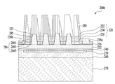
- FIG. 2 is a view showing a first embodiment of a light emitting device.
- the second conductive layer 236 is disposed under the light emitting structure 220, and the insulating layer 285 and the first conductive layer are disposed below the second conductive layer 236.
- 232 is disposed, and the through electrode 233 extending from the first conductive layer 232 may be in electrical contact with the second conductivity-type semiconductor layer 222 in the light emitting structure 220.
- the second electrodes 236a and 236b may be disposed to correspond to the edges of the light emitting structure 220.
- the light emitting structure 220 includes a first conductive semiconductor layer 222, an active layer 224, and a second conductive semiconductor layer 226.
- the first conductive semiconductor layer 222 may be formed of a compound semiconductor such as a III-V group or a II-VI group, and may be doped with the first conductive dopant.
- the first conductive semiconductor layer 222 is a semiconductor material having Al x In y Ga (1-xy) N (0 ⁇ x ⁇ 1, 0 ⁇ y ⁇ 1, 0 ⁇ x + y ⁇ 1), and AlGaN.
- GaN, InAlGaN, AlGaAs, GaP, GaAs, GaAsP, AlGaInP may be formed of any one or more.
- the first conductivity type dopant may include an n type dopant such as Si, Ge, Sn, Se, Te, or the like.
- the first conductivity type semiconductor layer 222 may be formed as a single layer or a multilayer, but is not limited thereto.
- the active layer 224 is disposed between the first conductivity type semiconductor layer 222 and the second conductivity type semiconductor layer 226, and has a single well structure, a multi well structure, a single quantum well structure, and a multi quantum well.
- a multi-quantum well (MQW) structure, a quantum dot structure or a quantum line structure may be included.
- the active layer 224 may be formed of a well layer and a barrier layer, for example, AlGaN / AlGaN, InGaN / GaN, InGaN / InGaN, AlGaN / GaN, InAlGaN / GaN, GaAs (InGaAs) using a compound semiconductor material of a group III-V element.
- a barrier layer for example, AlGaN / AlGaN, InGaN / GaN, InGaN / InGaN, AlGaN / GaN, InAlGaN / GaN, GaAs (InGaAs) using a compound semiconductor material of a group III-V element.
- / AlGaAs, GaP (InGaP) / AlGaP may be formed of any one or more pair structure, but is not limited thereto.
- the well layer may be formed of a material having an energy band gap smaller than the energy band gap of the barrier layer.
- the second conductivity type semiconductor layer 226 may be formed of a semiconductor compound.
- the second conductive semiconductor layer 226 may be formed of a compound semiconductor such as a III-V group or a II-VI group, and may be doped with a second conductive dopant.
- the second conductivity-type semiconductor layer 226 is, for example, a semiconductor material having a compositional formula of In x Al y Ga 1- xy N (0 ⁇ x ⁇ 1, 0 ⁇ y ⁇ 1, 0 ⁇ x + y ⁇ 1), AlGaN It may be formed of any one or more of, GaNAlInN, AlGaAs, GaP, GaAs, GaAsP, AlGaInP.
- the second conductive dopant may be a p-type dopant such as Mg, Zn, Ca, Sr, or Ba.
- the second conductivity-type semiconductor layer 226 may be formed as a single layer or a multilayer, but is not limited thereto.
- the light emitting structure 220 is grown based on AlGaN and, for example, the composition ratio of aluminum (Al) in AlGaN. May be greater than or equal to 40%, and light emission in a TM mode in which light emission in a vertical direction parallel to a growth direction of the light emitting structure 220 is superior to light emitting devices emitting light in a blue wavelength region may be increased. In this case, due to the light extraction structure described above, reabsorption of light in the light emitting structure 220 may be reduced.
- an electron blocking layer may be disposed between the active layer 224 and the second conductive semiconductor layer 226.
- the electron blocking layer may have a superlattice structure, for example, AlGaN doped with a second conductivity type dopant may be disposed, and GaN having a different composition ratio of aluminum may be formed as a layer. It may be arranged alternately with each other.
- the surface of the first conductive semiconductor layer 222 may be uneven to improve light extraction efficiency.
- the second conductive layer 236 may be disposed under the second conductive semiconductor layer 226.
- the second conductive layer 236 may be disposed in surface contact with the second conductive semiconductor layer 226, but may not be the area where the through electrode 233 is formed.
- an edge of the second conductive layer 236 may be disposed outside the edge of the second conductive semiconductor layer 226 to secure an area where the second electrodes 236a and 236b are to be disposed. to be.
- the second conductive layer 236 may be made of a conductive material, and in detail, may be made of a metal, and more specifically, silver (Ag), aluminum (Al), titanium (Ti), chromium (Cr), and nickel ( Ni), copper (Cu), and gold (Au) may be formed to have a single layer or a multilayer structure.
- the passivation layer 280 may be formed around the light emitting structure 220.
- the passivation layer 280 may be made of an insulating material, and the insulating material may be made of an oxide or nitride which is non-conductive.
- the passivation layer 280 may be formed of a silicon oxide (SiO 2 ) layer, an oxynitride layer, or an aluminum oxide layer.
- the passivation layer 280 may also be disposed on the circumference of the light emitting structure 220 and on the edge of the second conductive layer 236 disposed outside the edge of the second conductive semiconductor layer 226 described above. have.
- the passivation layer 280 disposed on the edge of the second conductive layer 236 may be open in a region where the second electrodes 236a and 236b are formed.
- the first conductive layer 232 may be disposed below the second conductive layer 236 with the insulating layer 285 interposed therebetween, and the first conductive layer 232 may be made of a conductive material. It may be made of a metal, more specifically, including at least one of silver (Ag), aluminum (Al), titanium (Ti), chromium (Cr), nickel (Ni), copper (Cu), gold (Au) It may be formed in a single layer or a multilayer structure.
- the plurality of through electrodes 233 extend from the first conductive layer 232 to the top, and the through electrodes 233 are the insulating layer 285, the second conductive layer 236, and the second conductive semiconductor layer ( Penetrates through the 226 and the active layer 224 and extends to a part of the first conductive semiconductor layer 222 so that the top surface of the through electrode 233 is in surface contact with the first conductive semiconductor layer 222. .
- each through electrode 233 may be circular or polygonal.
- the insulating layer 285 described above is disposed to extend around the through electrode 233, and the through electrode 233 is formed with the second conductive layer 236, the second conductive semiconductor layer 226, and the active layer 224. It can be electrically insulated.
- an ohmic layer 240 is disposed below the first conductive layer 232, and the ohmic layer is disposed between the first conductive layer 232 and the first conductive semiconductor layer 222 or the second conductive layer ( 236 and the second conductivity-type semiconductor layer 226 may be disposed.
- the ohmic layer 240 may be about 200 angstroms thick.
- the ohmic layer 240 may be formed of indium tin oxide (ITO), indium zinc oxide (IZO), indium zinc tin oxide (IZTO), indium aluminum zinc oxide (IAZO), indium gallium zinc oxide (IGZO), and indium gallium tin oxide (IGTO).
- ITO indium tin oxide
- IZO indium zinc oxide
- IZTO indium zinc tin oxide
- IAZO indium aluminum zinc oxide
- IGZO indium gallium zinc oxide
- IGTO indium gallium tin oxide
- a reflective layer 250 may be disposed below the ohmic layer, which may serve as a reflective electrode.
- the reflective layer 250 may include tungsten (W), titanium (Ti), molybdenum (Mo), aluminum (Al), silver (Ag), nickel (Ni), platinum (Pt), rhodium (Rh), or Al or Ag. It may be made of a metal layer containing an alloy containing Pt or Rh. Aluminum, silver, and the like may effectively reflect light propagated in the lower direction of FIG. 2 from the active layer 224, thereby greatly improving the light extraction efficiency of the semiconductor device.
- the width of the reflective layer 250 may be smaller than the width of the ohmic layer 240, and the channel layer 260 may be disposed under the reflective layer 250.
- the width of the channel layer 260 is greater than the width of the reflective layer 250 and may surround the reflective layer 250.
- the channel layer 260 may be made of a conductive material, for example, gold (Au) or tin (Sn).
- the conductive support substrate 270 may be formed of a conductive material such as a metal or a semiconductor material.
- a metal having excellent electrical conductivity or thermal conductivity may be used, and since it is necessary to sufficiently dissipate heat generated during operation of the semiconductor device, it may be formed of a material having high thermal conductivity (eg, a metal).
- a metal may be made of a material selected from the group consisting of molybdenum (Mo), silicon (Si), tungsten (W), copper (Cu), and aluminum (Al) or alloys thereof, and also gold (Au). ), Copper alloy (Cu Alloy), nickel (Ni), copper-tungsten (Cu-W), carrier wafers (e.g. GaN, Si, Ge, GaAs, ZnO, SiGe, SiC, SiGe, Ga 2 O 3, etc.) And the like may optionally be included.
- the support substrate 270 may be 50 to 200 in order to have a mechanical strength sufficient to be separated into separate chips through a scribing process and a breaking process without causing warping of the entire nitride semiconductor. It can be made with a thickness of micrometers.
- the bonding layer combines the channel layer 260 and the conductive support substrate 270, including gold (Au), tin (Sn), indium (In), aluminum (Al), silicon (Si), and silver. It may be formed of a material selected from the group consisting of (Ag), nickel (Ni) and copper (Cu) or alloys thereof.
- a current is uniformly supplied to the entire area of the first conductivity-type semiconductor layer 222 through the through electrode 233 from the first conductive layer 232, and the second conductive layer ( The current may be evenly supplied to the entire region of the second conductive semiconductor layer 226 which is in surface contact with the 236.
- the second electrodes 236a and 236b may be disposed on the upper portion of the second conductive layer 236 around the light emitting structure 220, so that a current may be uniformly supplied to the entire area of the second conductive layer 236. .
- the frequency of bonding of the electrons injected through the first conductivity type semiconductor layer 222 and the holes injected through the second conductivity type semiconductor layer 226 in the active layer 224 increases, resulting from the active layer 224.
- the amount of light emitted may increase.
- FIG 3 is a view showing another embodiment of a light emitting device.
- the light emitting device 200b is similar to the embodiment of FIG. 2, but the first recess penetrates through the second conductive semiconductor layer 226 and the active layer 224 to form the first conductive semiconductor layer 222. And a second recess penetrates the first conductive semiconductor layer 222, the second conductive semiconductor layer 226, and the active layer 224 to a partial region of the insulating layer 285. There is a difference.
- the first recess is formed in the insulating layer 285, the second conductive layer 236, the second conductive semiconductor layer 226, the active layer 224, and the first conductive semiconductor layer 222 in the lower direction of the light emitting structure.
- the through electrode 233 and the first conductive layer 232 may be formed of the same material, and the through electrode 233 and the first conductive layer 232 may form a first electrode. Can be achieved.
- the first conductive layer 232 may serve as a first electrode, and the conductive support substrate 270 may be electrically connected to the first electrode 233.
- the second recess may be a structure in which the insulating layer 285 is exposed through the first conductive semiconductor layer 222, the active layer 224, and the second conductive semiconductor layer 226 in the upper direction of the light emitting structure. And act as a light extracting unit 286.
- the light extracting portion 286 is formed by forming a concave and a convex on the surface of the first conductivity-type semiconductor layer 222, and the convex portions are disposed to correspond to the through electrode 233 described above. They may be formed to be equivalent to the area between the through electrodes 233.
- Recesses may be formed on one surface of the insulating layer 285.
- the light extracting unit 286 includes a light extracting unit lower surface portion 2865 forming a lower surface of the light extracting unit 286, and a first light extracting unit provided to form one side of the light extracting unit 286.
- the second light extractor side surface portion 2863 may be provided to form the side portion 2861 and the other side of the light extractor 286, and the light extractor lower surface 2865 is formed of an insulating layer 285. Can be.
- the insulating layer 285 disposed in the region between the through electrodes 233 of the light emitting device 200a of FIG. 2 may be disposed in surface contact with the second conductive layer 236.
- the insulating layer 285 disposed in the region between the through electrodes 233 of the light emitting device 200b of FIG. 3 may be disposed to be open without contacting the second conductive layer 236. have.
- the first light extractor side portion 2861 and the second light extractor side portion 2863 may include a first conductive semiconductor layer 222, an active layer 224, and a second conductive semiconductor layer 226. Since both the first light extractor side portion 2861 and the second light extractor side portion 2863 are mesa-etched to open the active layer 224, the light generated from the active layer 224 may be more efficiently applied to the light emitting device 200b. It can be extracted toward the outside has the effect of increasing the light extraction efficiency of the light emitting device (200b).
- one surface of the active layer 224 is mesa-etched so that the light generated in the active layer 224 is extracted toward the outside of the light emitting device 200 without being absorbed and / or reflected by the first conductivity-type semiconductor layer 222. Therefore, the light extraction efficiency of the light emitting device 200 is increased.
- the light extracting unit 286 is illustrated as being all provided between the through electrodes 233.
- the light extracting unit 286 is illustrated in one embodiment, and the light generated from the active layer 224 is external to the light emitting device 200. 3 and 4 may not be limited, and the shape and number of light extracting units 286 may be provided differently according to a user's needs, and thus the present invention is not limited to the scope of the present invention. .
- FIG. 4 is a view showing in detail the light emitting structure of FIG.
- the light extraction unit 286 may be provided so as not to include the inflection point on the side.
- Unevenness may be formed in the region C where the through electrode 233 contacts the first conductivity-type semiconductor layer 222.
- Convex portions are formed on the surface of the first conductivity-type semiconductor layer 222 in correspondence with the through-electrode 233, and recesses are formed on the surface of the first conductivity-type semiconductor layer 222 in correspondence with the regions between the through-electrodes 233. Can be formed. In this case, irregularities may be formed on the surfaces B and A of the recessed portions and the convex portions, respectively.
- the pattern consisting of recesses and convex portions on the surface of the first conductive semiconductor layer 222 has regularity, but irregularities formed on the surfaces of each recess and convex portion may be irregular roughness.
- the width of the convex portion may be larger than the width of the through electrode 233. More specifically, the third width W 21 of the surface of the through electrode 233 may be smaller than the second width W 22 of the region where the through electrode 233 is in contact with the first conductive layer 232. The width W 11 of the surface of the convex portion may be greater than the width W 12 of the lower surface of the light extracting portion at a height corresponding to the surface of the adjacent recessed portion.
- the width W 11 of the surface of the convex portion may be wider than the third width W 21 of the surface of the through electrode 233, and the first electrode 233 may contact the first conductive layer 232.
- the width W 12 of the bottom surface of the light extraction portion at a height corresponding to the surface of the adjacent recessed portion may be narrower than the two widths W 22 .
- the width of the light extracting lower surface 2865 may be disposed to have a first width W 12 for extracting light generated from the active layer 224.
- the first width W 12 of the light extracting lower surface 2865 may be provided to be 3 ⁇ m or more.
- the center distance W 3 between the through electrodes 223 may be provided to be 50um to 200um.
- center distance W 3 between the through electrodes 223 is provided to be 200 ⁇ m or more, a problem occurs in that light extraction efficiency is reduced due to a decrease in current spread characteristics of the first conductive semiconductor layer 222. do.
- the first angle formed by the insulating layer 285, the first light extractor side portion 2861, and the second light extractor side portion 2863 may be 80 ° or less.
- the angle formed between the insulating layer 285, the first light extractor side portion 2861, and the second light extractor side portion 2863 is 80 ° or more, the light extracted through the first light extractor side portion 2861 is provided. This is because the light extraction efficiency is reduced by being reabsorbed to the second light extracting side surface portion 2853 again.
- an angle formed between the insulating layer 285, the first light extracting part side portion 2861, and the second light extracting part side portion 2863 is 80 ° or less, thereby increasing light extraction efficiency of the light emitting device 200c. It works.
- 5A to 5D illustrate various embodiments of the light emitting structure of FIG. 4.
- the first and second light extracting side surfaces 2861 and 2863 may be provided in various shapes.
- first and second light extracting side surfaces 2861 and 2863 of the embodiment may be provided to include roughness on a surface thereof.
- the top surface of the second conductive semiconductor layer 222 is provided with roughness but also the first and second light extracting side surfaces 2861 and 2863 are provided with roughness to see light emitted from the active layer 224. It is effective to extract efficiently.
- the side surfaces 2861 and 2863 of the first and second light extracting units of the embodiment may be provided in a stepped form, or may be provided in a concave or convex form.
- the light is extracted more efficiently, thereby improving the light extraction efficiency of the light emitting device.
- first and second light extracting side surfaces 2861 and 2863 may be provided differently according to the needs of the user, and the scope of the present invention is not limited.
- FIGS. 6A and 6B are top views of the light emitting device of FIGS. 2 and 3.
- through electrodes 233 are disposed under the first conductivity type semiconductor layer 222, and an insulating layer 285 is disposed around each through electrode 233.
- the through electrode 233 and the insulating layer 285 may be disposed below the first conductivity type semiconductor layer 222 and may not be visible from the top view, but are shown for convenience of understanding.
- Second electrodes 236a and 236b are disposed outside the passivation layer 280.
- the second electrode 236b disposed in the 'D' region is larger than the second electrode 236a disposed in the region having a different width, and may be a region to which the wire is to be bonded.
- recesses may be disposed in region 'B' of the surface of the second conductivity-type semiconductor layer 222, and the recesses may be disposed between the through electrodes 233.
- the through-electrode 233 connected to the first conductive semiconductor layer 222 from the first conductive layer 232 is evenly disposed in the entire region, and thus the first conductive Current is uniformly supplied to the entire region of the type semiconductor layer 222, and thus, light emission efficiency may be improved by smoothly combining electrons and holes in the entire region of the light emitting structure 220.
- FIG. 7 is a view showing an embodiment of a light emitting device package.
- the light emitting device package 300 includes a package body 310, a first electrode part 321, a second electrode part 322, and a light emitting device 200.
- the package body 310 may be made of an insulating material having a cavity, and may include, for example, a polypthalamide (PPA) resin or a silicon-based material.
- PPA polypthalamide
- the first electrode part 321 and the second electrode part 322 may be disposed on the package body 310, respectively, and part of the first electrode part 321 and the second electrode part 322 may be disposed on the bottom surface of the cavity.
- the light emitting device 200 may be the above-described light emitting device, and may be disposed on the first electrode part 321 and electrically connected to the second electrode part 322 through a wire 330.
- the molding part 350 is disposed around the light emitting device 200 and the wire 330, and the molding part 350 may be filled with air or made of another protective material.
- the molding part 350 may include a phosphor (not shown).
- the phosphor may be used as a yag-based phosphor, a nitride-based phosphor, a silicate, or a mixture thereof, but is not limited thereto.
- the cover 370 is disposed on the package 300, and the cover 370 may be made of a light transmissive material such as glass.
- the light emitting device may be flip bonded and used as a package.
- a plurality of light emitting device packages according to the embodiment may be arranged on a substrate, and a light guide plate, a prism sheet, a diffusion sheet, or the like, which is an optical member, may be disposed on an optical path of the light emitting device package.
- the light emitting device package, the substrate, and the optical member may function as a backlight unit.
- the display device may include a display device, an indicator device, and a lighting device including a light emitting device package according to an exemplary embodiment.
- the display device may include a bottom cover, a reflector disposed on the bottom cover, a light emitting module for emitting light, a light guide plate disposed in front of the reflector, and guiding light emitted from the light emitting module to the front, and in front of the light guide plate.
- An optical sheet including prism sheets disposed, a display panel disposed in front of the optical sheet, an image signal output circuit connected to the display panel and supplying an image signal to the display panel, and a color filter disposed in front of the display panel. It may include.
- the bottom cover, the reflector, the light emitting module, the light guide plate, and the optical sheet may form a backlight unit.
- the lighting apparatus includes a light source module including a substrate and a light emitting device package according to an embodiment, a heat sink for dissipating heat from the light source module, and a power supply unit for processing or converting an electrical signal provided from the outside and providing the light source module to the light source module.
- a light source module including a substrate and a light emitting device package according to an embodiment, a heat sink for dissipating heat from the light source module, and a power supply unit for processing or converting an electrical signal provided from the outside and providing the light source module to the light source module.
- the lighting device may include a lamp, a head lamp, or a street lamp.
- the head lamp includes a light emitting module including light emitting device packages disposed on a substrate, a reflector for reflecting light emitted from the light emitting module in a predetermined direction, for example, a lens for refracting the light reflected by the reflector forward. And a shade for blocking or reflecting a part of the light reflected by the reflector toward the lens to achieve a light distribution pattern desired by the designer.
- a light emitting device having a higher light extraction efficiency may be mounted on a light emitting device package by increasing light extraction efficiency according to an embodiment, and may be implemented as a display device, an indicator device, and a lighting device including the light emitting device package.
Landscapes
- Engineering & Computer Science (AREA)
- Microelectronics & Electronic Packaging (AREA)
- Manufacturing & Machinery (AREA)
- Computer Hardware Design (AREA)
- Power Engineering (AREA)
- Led Devices (AREA)
- Led Device Packages (AREA)
Abstract
실시예는 제1 도전형 반도체층, 제2 도전형 반도체층, 상기 제1 도전형 반도체층과 상기 제2 도전형 반도체층의 사이에 배치되는 활성층을 포함하고, 상기 제2 도전형 반도체층과 상기 활성층을 관통하여 상기 제1 도전형 반도체층의 일부 영역까지 배치되는 복수 개의 제1 리세스를 포함하는 발광 구조물; 상기 복수 개의 제1 리세스 내부에서 상기 제1 도전형 반도체층과 전기적으로 연결되는 제1 전극; 상기 제1 전극과 전기적으로 연결되는 도전성 지지 기판; 상기 제2 도전형 반도체층과 전기적으로 연결되는 제2 전극; 및 상기 도전성 지지 기판과 상기 제2 도전형 반도체층 사이에 배치되는 절연층을 포함하고, 상기 제1 도전형 반도체층과 상기 제2 도전형 반도체층 및 상기 활성층을 관통하여 상기 절연층의 일부 영역까지 제2 리세스가 배치되는 발광소자에 관한 것이다.
Description
실시예는 발광소자에 관한 것이다.
GaN, AlGaN 등의 3-5족 화합물 반도체는 넓고 조정이 용이한 밴드 갭 에너지를 가지는 등의 많은 장점으로 인해 광 전자 공학 분야(optoelectronics)와 전자 소자 등에 널리 사용된다.
특히, 반도체의 3-5족 또는 2-6족 화합물 반도체 물질을 이용한 발광 다이오드(Light Emitting Diode)나 레이저 다이오드와 같은 발광 소자는 박막 성장 기술 및 소자 재료의 개발로 적색, 녹색, 청색 및 자외선 등 다양한 색을 구현할 수 있으며, 형광 물질을 이용하거나 색을 조합함으로써 효율이 좋은 백색 광선도 구현이 가능하며, 형광등, 백열등 등 기존의 광원에 비해 저소비전력, 반영구적인 수명, 빠른 응답속도, 안전성, 환경친화성의 장점을 가진다.
따라서, 광 통신 수단의 송신 모듈, LCD(Liquid Crystal Display) 표시 장치의 백라이트를 구성하는 냉음극관(CCFL: Cold Cathode Fluorescence Lamp)을 대체하는 발광 다이오드 백라이트, 형광등이나 백열 전구를 대체할 수 있는 백색 발광 다이오드 조명 장치, 자동차 헤드 라이트 및 신호등에까지 응용이 확대되고 있다.
발광 소자는 제1 도전형 반도체층과 활성층 및 제2 도전형 반도체층을 포함하는 발광구조물이 형성되고, 제1 도전형 반도체층과 제2 도전형 반도체층 상에 각각 제1 전극과 제2 전극이 배치된다. 발광 소자는 제1 도전형 반도체층을 통해서 주입되는 전자와 제2 도전형 반도체층을 통해서 주입되는 정공이 서로 만나서 활성층을 이루는 물질 고유의 에너지 밴드에 의해서 결정되는 에너지를 갖는 빛을 방출한다. 활성층에서 방출되는 빛은 활성층을 이루는 물질의 조성에 따라 다를 수 있으며, 청색광이나 자외선(UV) 또는 심자외선(Deep UV) 등일 수 있다.
도 1은 종래의 발광소자를 나타낸 도면이다.
도 1에 도시된 수직형 발광소자는 제2 전극(136) 위에, 제1 도전형 반도체층(122)과 활성층(124) 및 제2 도전형 반도체층(126)을 포함하는 발광 구조물(120)이 배치되고, 상기 제1 도전형 반도체층(122) 상에 제1 전극(132)이 배치된다.
종래의 발광소자는 활성층(124)에서 빛이 발광하는데, 활성층(124)에서 발광된 빛이 제1 전극(132)에 의해 흡수되어 광 추출 효율이 떨어지는 문제가 있었다.
실시 예의 발광소자는 보다 높은 광 추출 효율을 갖는 발광소자를 제공한다.
실시 예의 발광소자는 상술한 문제를 해결하기 위하여, 제1 도전형 반도체층, 제2 도전형 반도체층, 상기 제1 도전형 반도체층과 상기 제2 도전형 반도체층의 사이에 배치되는 활성층을 포함하고, 상기 제2 도전형 반도체층과 상기 활성층을 관통하여 상기 제1 도전형 반도체층의 일부 영역까지 배치되는 복수 개의 제1 리세스를 포함하는 발광 구조물; 상기 복수 개의 제1 리세스 내부에서 상기 제1 도전형 반도체층과 전기적으로 연결되는 제1 전극; 상기 제1 전극과 전기적으로 연결되는 도전성 지지 기판; 상기 제2 도전형 반도체층과 전기적으로 연결되는 제2 전극; 및 상기 도전성 지지 기판과 상기 제2 도전형 반도체층 사이에 배치되는 절연층을 포함하고, 상기 제1 도전형 반도체층과 상기 제2 도전형 반도체층 및 상기 활성층을 관통하여 상기 절연층의 일부 영역까지 제2 리세스가 배치되는 발광소자를 제공하는 것을 과제의 해결 수단으로 한다.
또한, 상기 절연층은 상기 제1 리세스의 둘레에 연장되어 배치된 발광소자를 제공하는 것을 과제의 해결 수단으로 한다.
또한, 상기 제2 리세스는 상기 제2 리세스의 하부면을 형성하는 광 추출부 하부면, 상기 제2 리세스의 일 측면을 형성하는 제1광 추출부 측면부 및 상기 제2 리세스의 다른 측면을 형성하는 제2광 추출부 측면부를 포함하는 발광소자를 제공하는 것을 과제의 해결 수단으로 한다.
또한, 상기 광 추출부 하부면은 상기 절연층인 발광소자를 제공하는 것을 과제의 해결 수단으로 한다.
또한, 상기 광 추출부 하부면의 폭은 상기 활성층에서 발생하는 광을 추출하기 위한 제1폭을 갖도록 배치되는 발광소자를 제공하는 것을 과제의 해결 수단으로 한다.
또한, 상기 제1폭은 3um이상인 발광소자를 제공하는 것을 과제의 해결 수단으로 한다.
또한, 상기 제1광 추출부 측면부는 상기 절연층과 상기 활성층에서 발생하는 광이 상기 제2광 추출부 측면부로 재흡수 되지 않게 하기 위한 제1각도를 갖도록 배치되는 발광 소자를 제공하는 것을 과제의 해결 수단으로 한다.
또한, 상기 제1각도는 80도 이하인 발광소자를 제공하는 것을 과제의 해결 수단으로 한다.
또한, 상기 제1 리세스의 표면의 제3 폭은, 상기 제1 리세스가 상기 제1 전극과 접촉하는 영역의 제2 폭보다 작은 발광소자를 제공하는 것을 과제의 해결 수단으로 한다.
또한, 상기 발광 구조물은 UV-B 또는 UV-C 파장 영역의 광을 방출하는 발광소자를 제공하는 것을 과제의 해결 수단으로 한다.
또한, 상기 제1 도전형 반도체층 또는 제2 도전형 반도체층 내에서 알루미늄(Al)의 조성비는 40% 이상인 발광소자를 제공하는 것을 과제의 해결 수단으로 한다.
또한, 제1 도전형 반도체층, 제2 도전형 반도체층, 및 상기 제1 도전형 반도체층과 상기 및 제2 도전형 반도체층 사이에 배치되는 활성층을 포함하고, 상기 제2 도전형 반도체층과 상기 활성층을 관통하여 상기 제1 도전형 반도체층의 일부 영역까지 배치되는 복수 개의 제1 리세스를 포함하는 발광 구조물; 상기 복수 개의 제1 리세스 내부에서 상기 제1 도전형 반도체층과 전기적으로 연결되는 제1 전극; 상기 제1 전극과 전기적으로 연결되는 도전성 지지 기판; 상기 제2 도전형 반도체층과 전기적으로 연결되는 제2 전극; 및 상기 도전성 지지 기판과 상기 제2 도전형 반도체층 사이에 배치되는 절연층을 포함하고 상기 제1 도전형 반도체층과 상기 제2 도전형 반도체층 및 상기 활성층을 관통하여 상기 절연층의 일부 영역까지 제2 리세스가 배치되고, 상기 제2 리세스는, 상기 제2 리세스의 하부면을 형성하는 광 추출부 하부면, 상기 제2 리세스의 일 측면을 형성하는 제1광 추출부 측면부, 및 상기 제2 리세스의 다른 측면을 형성하는 제2광 추출부 측면부를 포함하고, 상기 광 추출부 하부면은 상기 활성층에서 발생하는 광을 추출하기 위한 제1폭을 갖고, 상기 제1폭은 3um이상이고, 상기 제1 리세스의 표면의 제3 폭은 상기 제1 리세스가 상기 제1 전극과 접촉하는 영역의 제2 폭보다 작은 발광소자를 제공하는 것을 과제의 해결 수단으로 한다.
또한, 캐비티가 형성된 도전성 기판 및 상기 도전성 기판의 캐비티에 적어도 일부가 삽입되어 배치되는 발광소자를 포함하고, 상기 발광소자는 제1 도전형 반도체층, 제2 도전형 반도체층, 상기 제1 도전형 반도체층과 상기 제2 도전형 반도체층의 사이에 배치되는 활성층을 포함하고, 상기 제2 도전형 반도체층과 상기 활성층을 관통하여 상기 제1 도전형 반도체층의 일부 영역까지 배치되는 복수 개의 제1 리세스를 포함하는 발광 구조물; 상기 복수 개의 제1 리세스 내부에서 상기 제1 도전형 반도체층과 전기적으로 연결되는 제1 전극; 상기 제1 전극과 전기적으로 연결되는 도전성 지지 기판; 상기 제2 도전형 반도체층과 전기적으로 연결되는 제2 전극; 및 상기 도전성 지지 기판과 상기 제2 도전형 반도체층 사이에 배치되는 절연층을 포함하고 상기 제1 도전형 반도체층과 상기 제2 도전형 반도체층 및 상기 활성층을 관통하여 상기 절연층의 일부 영역까지 제2 리세스가 배치되는 발광소자 패키지를 제공하는 것을 과제의 해결 수단으로 한다.
또한, 상기 제2 리세스는 상기 광 추출부의 하부면을 형성하는 광 추출부 하부면, 상기 광 추출부의 일 측면을 형성하는 제1광 추출부 측면부 및 상기 광 추출부의 다른 측면을 형성하는 제2광 추출부 측면부를 포함하는 발광소자 패키지를 제공하는 것을 과제의 해결 수단으로 한다.
또한, 상기 광 추출부 하부면은 상기 절연층인 발광소자 패키지를 제공하는 것을 과제의 해결 수단으로 한다.
또한, 상기 광 추출부 하부면의 폭은 상기 활성층에서 발생하는 광을 추출하기 위한 제1폭을 갖도록 배치되는 발광소자 패키지를 제공하는 것을 과제의 해결 수단으로 한다.
또한, 상기 제1폭은 3um이상인 발광소자 패키지를 제공하는 것을 과제의 해결 수단으로 한다.
또한, 상기 제1광 추출부 측면부는 상기 절연층과 상기 활성층에서 발생하는 광이 상기 제2광 추출부 측면부로 재흡수 되지 않게 하기 위한 제1각도를 갖도록 배치되는 발광 소자 패키지를 제공하는 것을 과제의 해결 수단으로 한다.
또한, 상기 제1각도는 80도 이하인 발광소자 패키지를 제공하는 것을 과제의 해결 수단으로 한다.
또한, 상기 제1 도전형 반도체층 또는 제2 도전형 반도체층 내에서 알루미늄(Al)의 조성비는 40% 이상인 발광소자 패키지를 제공하는 것을 과제의 해결 수단으로 한다.
본 실시예들에 따른 발광소자들은 제1 도전형 반도체층에 배치되는 광 출구 구조를 포함하여, 활성층에서 생성된 광의 추출효율을 높여 보다 높은 광 추출 효율을 갖는 발광소자를 제공하는 것을 발명의 효과로 한다.
도 1은 종래의 발광소자를 나타낸 도면이고,
도 2는 발광소자의 일 실시예를 나타낸 도면이고,
도 3은 발광소자의 다른 실시예를 나타낸 도면이고,
도 4는 도 3의 발광 구조물을 상세히 나타낸 도면이고,
도 5a 내지 도 5d는 도 4의 발광구조물의 다양한 실시 예를 나타낸 도면이며,
도 6a 및 도 6b는 도 2 및 도 3의 발광소자의 상면도이고,
도 7은 발광소자 패키지의 일실시예를 나타낸 도면이다.
이하 상기의 목적을 구체적으로 실현할 수 있는 본 발명의 실시예를 첨부한 도면을 참조하여 설명한다.
본 발명에 따른 실시예의 설명에 있어서, 각 element의 " 상(위) 또는 하(아래)(on or under)"에 형성되는 것으로 기재되는 경우에 있어, 상(위) 또는 하(아래)(on or under)는 두 개의 element가 서로 직접(directly) 접촉되거나 하나 이상의 다른 element가 상기 두 element 사이에 배치되어(indirectly) 형성되는 것을 모두 포함한다. 또한 “상(위) 또는 하(아래)(on or under)”으로 표현되는 경우 하나의 element를 기준으로 위쪽 방향뿐만 아니라 아래쪽 방향의 의미도 포함할 수 있다.
실시예들에 따른 발광소자는 수직형 발광소자이되, 제1 도전형 반도체층에 전류를 공급하는 제1 전극이 발광 구조물의 하부에 배치되어 발광 구조물 상부로 방출되는 빛의 반사량을 줄일 수 있으며, 제1 전극은 제2 도전형 반도체층과 활성층을 관통하여 제1 도전형 반도체층에 전기적으로 연결될 수 있다.
도 2는 발광소자의 제1 실시예를 나타낸 도면이다.
본 실시예에 따른 발광소자(200a)는 발광 구조물(220)의 하부에 제2 도전층(236)이 배치되고, 제2 도전층(236)의 하부에는 절연층(285)과 제1 도전층(232)이 배치되며, 제1 도전층(232)으로부터 연장된 관통 전극(233)이 발광 구조물(220) 내의 제2 도전형 반도체층(222)과 전기적으로 접촉할 수 있다. 그리고, 제2 도전층(236)의 가장 자리 영역에서 제2 전극(236a, 236b)이 발광 구조물(220)의 가장 자리와 대응하여 배치될 수 있다.
발광 구조물(220)은 제1 도전형 반도체층(222)과 활성층(224) 및 제2 도전형 반도체층(226)을 포함하여 이루어진다.
제1 도전형 반도체층(222)은 Ⅲ-Ⅴ족, Ⅱ-Ⅵ족 등의 화합물 반도체로 구현될 수 있으며, 제1 도전형 도펀트가 도핑될 수 있다. 제1 도전형 반도체층(222)은 AlxInyGa(1-x-y)N (0≤x≤1, 0≤y≤1, 0≤x+y≤1)의 조성식을 갖는 반도체 물질, AlGaN, GaN, InAlGaN, AlGaAs, GaP, GaAs, GaAsP, AlGaInP 중 어느 하나 이상으로 형성될 수 있다.
제1 도전형 반도체층(222)이 n형 반도체층인 경우, 제1 도전형 도펀트는 Si, Ge, Sn, Se, Te 등과 같은 n형 도펀트를 포함할 수 있다. 제1 도전형 반도체층(222)은 단층 또는 다층으로 형성될 수 있으며, 이에 대해 한정하지는 않는다.
활성층(224)은 제1 도전형 반도체층(222)과 제2 도전형 반도체층(226) 사이에 배치되며, 단일 우물 구조(Double Hetero Structure), 다중 우물 구조, 단일 양자 우물 구조, 다중 양자 우물(MQW:Multi Quantum Well) 구조, 양자점 구조 또는 양자선 구조 중 어느 하나를 포함할 수 있다.
활성층(224)은 Ⅲ-Ⅴ족 원소의 화합물 반도체 재료를 이용하여 우물층과 장벽층, 예를 들면 AlGaN/AlGaN, InGaN/GaN, InGaN/InGaN, AlGaN/GaN, InAlGaN/GaN, GaAs(InGaAs)/AlGaAs, GaP(InGaP)/AlGaP 중 어느 하나 이상의 페어 구조로 형성될 수 있으나 이에 한정되지는 않는다. 이때, 우물층은 장벽층의 에너지 밴드 갭보다 작은 에너지 밴드 갭을 갖는 물질로 형성될 수 있다.
제2 도전형 반도체층(226)은 반도체 화합물로 형성될 수 있다. 제2 도전형 반도체층(226)은 Ⅲ-Ⅴ족, Ⅱ-Ⅵ족 등의 화합물 반도체로 구현될 수 있으며, 제2 도전형 도펀트가 도핑될 수 있다. 제2 도전형 반도체층(226)은 예컨대, InxAlyGa1
-x-yN (0≤x≤1, 0≤y≤1, 0≤x+y≤1)의 조성식을 갖는 반도체 물질, AlGaN, GaNAlInN, AlGaAs, GaP, GaAs, GaAsP, AlGaInP 중 어느 하나 이상으로 형성될 수 있다.
제2 도전형 반도체층(226)이 p형 반도체층인 경우, 제2 도전형 도펀트는 Mg, Zn, Ca, Sr, Ba 등과 같은 p형 도펀트일 수 있다. 제2 도전형 반도체층(226)은 단층 또는 다층으로 형성될 수 있으며, 이에 대해 한정하지는 않는다.
실시예에 따른 발광 소자(200a)가 UV-B나 UV-C 파장 영역의 광을 방출할 경우, AlGaN을 기반으로 발광 구조물(220)이 성장되고 예를 들면 AlGaN 내에서 알루미늄(Al)의 조성비는 40% 이상일 수 있는데, 청색 파장 영역의 광을 방출하는 발광소자에 비하여 발광 구조물(220)의 성장 방향과 평행한 수직한 방향의 발광이 우세한 TM 모드의 발광이 증가할 수 있다. 이때, 상술한 광추출 구조로 인하여 발광 구조물(220) 내에서 광의 재흡수를 줄일 수 있다.
도시되지는 않았으나, 활성층(224)과 제2 도전형 반도체층(226)의 사이에는 전자 차단층(Electron blocking layer)가 배치될 수 있다. 전자 차단층은 초격자(superlattice) 구조로 이루어질 수 있는데, 초격자는 예를 들어 제2 도전형 도펀트로 도핑된 AlGaN이 배치될 수 있고, 알루미늄의 조성비를 달리하는 GaN이 층(layer)을 이루어 복수 개 서로 교번하여 배치될 수도 있다.
제1 도전형 반도체층(222)의 표면이 도시된 바와 같이 요철을 이루어 광추출 효율을 향상시킬 수 있다.
제2 도전형 반도체층(226)의 하부에는 제2 도전층(236)이 배치될 수 있다. 제2 도전층(236)은 제2 도전형 반도체층(226)과 면접촉하며 배치되되, 관통 전극(233)이 형성된 영역에서는 그러하지 않을 수 있다. 그리고, 제2 도전층(236)의 가장 자리는 제2 도전형 반도체층(226)의 가장 자리보다 더 외곽에 배치될 수 있는데, 제2 전극(236a, 236b)이 배치될 영역을 확보하기 위함이다.
제2 도전층(236)은 도전성 물질로 이루어질 수 있고, 상세하게는 금속으로 이루어질 수 있으며, 보다 상세하게는 은(Ag), 알루미늄(Al), 티타늄(Ti), 크롬(Cr), 니켈(Ni), 구리(Cu), 금(Au) 중 적어도 하나를 포함하여 단층 또는 다층 구조로 형성될 수 있다.
발광 구조물(220)의 둘레에는 패시베이션층(280)이 형성될 수 있는데, 패시베이션층(280)은 절연물질로 이루어질 수 있으며, 절연물질은 비전도성인 산화물이나 질화물로 이루어질 수 있다. 일 예로서, 패시베이션층(280)은 실리콘 산화물(SiO2)층, 산화 질화물층, 산화 알루미늄층으로 이루어질 수 있다.
패시베이션층(280)은 발광 구조물(220)의 둘레와, 상술한 제2 도전형 반도체층(226)의 가장 자리보다 더 외곽에 배치된 제2 도전층(236)의 가장 자리 상에도 배치될 수 있다. 제2 도전층(236)의 가장 자리 상에 배치된 패시베이션층(280)은 제2 전극(236a, 236b)이 형성된 영역에서는 오픈(open)될 수 있다.
제2 도전층(236)의 하부에는 절연층(285)을 사이에 두고 제1 도전층(232)이 배치될 수 있으며, 제1 도전층(232)은 도전성 물질로 이루어질 수 있고, 상세하게는 금속으로 이루어질 수 있으며, 보다 상세하게는 은(Ag), 알루미늄(Al), 티타늄(Ti), 크롬(Cr), 니켈(Ni), 구리(Cu), 금(Au) 중 적어도 하나를 포함하여 단층 또는 다층 구조로 형성될 수 있다.
제1 도전층(232)으로부터 상부로 연장되어 복수 개의 관통 전극(233)들이 배치되는데, 관통 전극(233)들은 절연층(285)과 제2 도전층(236)과 제2 도전형 반도체층(226)과 활성층(224)을 관통하고, 제1 도전형 반도체층(222)의 일부에까지 연장되어, 관통 전극(233)의 상부면이 제1 도전형 반도체층(222)과 면접촉할 수 있다.
각각의 관통 전극(233)의 단면은 원형이거나 다각형일 수 있다. 상술한 절연층(285)은 관통 전극(233)의 둘레에 연장되어 배치되어, 관통 전극(233)을 제2 도전층(236), 제2 도전형 반도체층(226) 및 활성층(224)과 전기적으로 절연시킬 수 있다.
도 2에서 제1 도전층(232)의 하부에는 오믹층(240)이 배치되는데, 오믹층은 제1 도전층(232)과 제1 도전형 반도체층(222)의 사이 또는 제2 도전층(236)과 제2 도전형 반도체층(226)의 사이에 배치될 수 있다.
오믹층(240)은 약 200 옹스트롬의 두께일 수 있다. 오믹층(240)은 ITO(indium tin oxide), IZO(indium zinc oxide), IZTO(indium zinc tin oxide), IAZO(indium aluminum zinc oxide), IGZO(indium gallium zinc oxide), IGTO(indium gallium tin oxide), AZO(aluminum zinc oxide), ATO(antimony tin oxide), GZO(gallium zinc oxide), IZON(IZO Nitride), AGZO(Al-GaZnO), IGZO(In-GaZnO), ZnO, IrOx, RuOx, NiO, RuOx/ITO, Ni/IrOx/Au, 및 Ni/IrOx/Au/ITO, Ag, Ni, Cr, Ti, Al, Rh, Pd, Ir, Sn, In, Ru, Mg, Zn, Pt, Au, Hf 중 적어도 하나를 포함하여 형성될 수 있으며, 이러한 재료에 한정되는 않는다.
오믹층의 하부에는 반사 전극으로 작용할 수 있는 반사층(250)이 배치될 수 있다. 반사층(250)은 텅스텐(W), 티타늄(Ti), 몰리브덴(Mo), 알루미늄(Al), 은(Ag), 니켈(Ni), 백금(Pt), 로듐(Rh), 혹은 Al이나 Ag이나 Pt나 Rh를 포함하는 합금을 포함하는 금속층으로 이루어질 수 있다. 알루미늄이나 은 등은 활성층(224)에서 도 2의 하부 방향으로 진행한 빛을 효과적으로 반사하여 반도체 소자의 광추출 효율을 크게 개선할 수 있다.
반사층(250)의 폭은 오믹층(240)의 폭보다 좁을 수 있으며, 반사층(250)의 하부에는 채널층(260)이 배치될 수 있다. 채널층(260)의 폭은 반사층(250)의 폭보다 커서 반사층(250)을 감싸며 배치될 수 있다. 채널층(260)은 도전성 물질로 이루어질 수 있으며, 예를 들면 금(Au)이나 주석(Sn)으로 이루어질 수 있다.
도전성 지지 기판(support substrate, 270)은 금속 또는 반도체 물질 등 도전성 물질로 형성될 수 있다. 전기 전도도 내지 열전도도가 우수한 금속을 사용할 수 있고, 반도체 소자 작동시 발생하는 열을 충분히 발산시킬 수 있어야 하므로 열 전도도가 높은 물질(ex. 금속 등)로 형성될 수 있다. 예를 들어, 몰리브덴(Mo), 실리콘(Si), 텅스텐(W), 구리(Cu) 및 알루미늄(Al)로 구성되는 군으로부터 선택되는 물질 또는 이들의 합금으로 이루어질 수 있으며, 또한, 금(Au), 구리합금(Cu Alloy), 니켈(Ni), 구리-텅스텐(Cu-W), 캐리어웨이퍼(예: GaN, Si, Ge, GaAs, ZnO, SiGe, SiC, SiGe, Ga2O3 등) 등을 선택적으로 포함할 수 있다.
상기 지지 기판(270)은 전체 질화물 반도체에 휨을 가져오지 않으면서, 스크라이빙(scribing) 공정 및 브레이킹(breaking) 공정을 통하여 별개의 칩으로 잘 분리시키기 위한 정도의 기계적 강도를 가지기 위하여 50 내지 200 마이크로 미터의 두께로 이루어질 수 있다.
도시되지는 않았으나, 접합층은 채널층(260)과 도전성 지지 기판(270)을 결합하는데, 금(Au), 주석(Sn), 인듐(In), 알루미늄(Al), 실리콘(Si), 은(Ag), 니켈(Ni) 및 구리(Cu)로 구성되는 군으로부터 선택되는 물질 또는 이들의 합금으로 형성할 수 있다.
본 실시예에 따른 발광소자(200a)에서 제1 도전층(232)으로부터 관통 전극(233)을 통하여 제1 도전형 반도체층(222)의 전체 영역에 고루 전류가 공급되며, 제2 도전층(236)과 면접촉하는 제2 도전형 반도체층(226)에도 전류가 전체 영역에 전류가 고루 공급될 수 있다. 또한, 제2 전극(236a, 236b)이 발광 구조물(220)의 둘레에서 제2 도전층(236)의 상부에 배치되어, 제2 도전층(236)의 전체 영역에 고루 전류가 공급될 수 있다. 따라서, 제1 도전형 반도체층(222)을 통해서 주입되는 전자와 제2 도전형 반도체층(226)을 통해서 주입되는 정공이 활성층(224) 내에서 결합하는 빈도가 증가하여, 활성층(224)으로부터 방출되는 광량이 증가할 수 있다.
도 3은 발광소자의 다른 실시 예를 나타낸 도면이다.
본 실시예에 따른 발광소자(200b)는 도 2의 실시예와 유사하되, 제1 리세스가 제2 도전형 반도체층(226)과 활성층(224)을 관통하여 제1 도전형 반도체층(222)의 일부 영역까지 배치되고, 제2 리세스가 제1 도전형 반도체층(222)과 제2 도전형 반도체층(226) 및 활성층(224)을 관통하여 절연층(285)의 일부 영역까지 배치되는 차이점이 있다.
제1 리세스는 발광 구조물의 하부 방향에서 절연층(285), 제2 도전층(236), 제2 도전형 반도체층(226), 활성층(224) 그리고 제1 도전형 반도체층(222)의 일부에까지 형성된 관통 전극의 가장 자리일 수 있으며, 관통 전극(233)과 제1 도전층(232)은 동일한 물질로 이루어지고, 관통 전극(233)과 제1 도전층(232)이 제1 전극을 이룰 수 있다.
그리고, 제1 도전층(232)은 제1 전극으로 작용할 수 있고, 도전성 지지 기판(270)은 제1 전극(233)과 전기적으로 연결될 수 있다.
제2 리세스는 발광 구조물의 상부 방향에서 제1 도전형 반도체층(222), 활성층(224), 제2 도전형 반도체층(226)을 관통하여 절연층(285)이 노출되도록 형성된 구조일 수 있으며, 광 추출부(286)로 작용할 수 있다.
광 추출부(286)는 제1 도전형 반도체층(222)의 표면에 요부(concave)와 철부(convex)가 형성되어 이루어지며, 철부들은 상술한 관통 전극(233)과 대응하며 배치되고, 요부들은 관통 전극(233) 사이의 영역과 대등하며 형성될 수 있다.
요부들은 절연층(285)의 일 면에 형성될 수 있다.
환언하면, 광 추출부(286)는 광 추출부(286)의 하부면을 형성하는 광 추출부 하부면부(2865), 광 추출부(286)의 일 측면을 형성하도록 구비되는 제1광 추출부 측면부(2861) 및 광 추출부(286)의 다른 측면을 형성하도록 구비되는 제2광 추출부 측면부(2863)을 포함할 수 있으며, 광 추출부 하부면(2865)은 절연층(285)으로 형성될 수 있다.
보다 자세하게는, 도 2에 도시된 실시 예의 발광소자(200a)의 관통 전극(233) 사이의 영역에 배치되는 절연층(285)은 제2 도전층(236)과 면 접촉 하도록 배치될 수 있는데, 도 3에 도시된 실시 예의 발광소자(200b)의 관통 전극(233)사이의 영역에 배치되는 절연층(285)은 제2 도전층(236)과 면 접촉 하지 아니하고 오픈(Open)되도록 배치될 수 있다.
제1광 추출부 측면부(2861) 및 제2광 추출부 측면부(2863)는 제1 도전형 반도체층(222), 활성층(224) 및 제 2 도전형 반도체층(226)을 포함할 수 있고, 제1광 추출부 측면부(2861) 및 제2광 추출부 측면부(2863)는 모두 메사 식각되어 활성층(224)이 오픈되기 때문에 활성층(224)에서 발생하는 광을 보다 효율적으로 발광소자(200b)의 외부를 향하여 추출 할 수 있어 발광소자(200b)의 광 추출 효율을 증가시키는 효과가 있다.
환언하자면, 활성층(224)의 일면이 메사 식각되어 활성층(224)에서 발생하는 빛이 제1 도전형 반도체층(222)에 의해 흡수 및/또는 반사 되지 아니하고 발광소자(200)의 외부를 향하여 추출 되기 때문에 발광소자(200)의 광 추출 효율이 증가하는 효과가 있다.
본 실시 예에서는 광 추출부(286)는 관통 전극(233)의 사이에 모두 구비되는 것으로 도시되었으나, 이는 일 실시 예를 도시한 것이고 활성층(224)에서 발생하는 광을 발광소자(200)의 외부로 추출 할 수 있으면 족하지 도 3 및 도 4에서 도시된 실시 예에 한정되지 아니하며 광 추출부(286)의 형상 및 개수는 사용자의 필요에 따라 다르게 구비될 수 있어 본 발명의 권리범위를 제한하지 아니한다.
도 4는 도 3의 발광 구조물을 상세히 나타낸 도면이다.
도 4를 참고하면, 도 3에 도시된 측면에 적어도 하나 이상의 변곡점을 포함하는 광 추출부(286)의 형상과 달리 광 추출부(286)는 측면에 변곡점을 포함하지 않도록 구비될 수도 있다.
관통 전극(233)이 제1 도전형 반도체층(222)과 접촉하는 영역(C)에는 요철이 형성될 수 있다.
관통 전극(233)과 대응하여 제1 도전형 반도체층(222)의 표면에 철부가 형성되고, 관통 전극(233)들 사이의 영역과 대응하여 제1 도전형 반도체층(222)의 표면에 요부가 형성될 수 있다. 이때, 요부와 철부들의 표면(B, A)에도 각각 요철이 형성될 수 있다.
제1 도전형 반도체층(222)의 표면의 요부와 철부로 이루어지는 패턴은 규칙성을 가지나, 각각의 요부와 철부의 표면에 형성되는 요철은 불규칙한 러프니스(roughness)일 수 있다.
도 4에서 철부의 폭은 관통 전극(233)의 폭보다 클 수 있다. 보다 상세하게는, 관통 전극(233)의 표면의 제3 폭(W21)은 관통 전극(233)이 제1 도전층(232)과 접촉하는 영역의 제2 폭(W22)보다 작을 수 있고, 철부의 표면의 폭(W11)은 인접한 요부의 표면에 대응하는 높이에서의 광 추출부 하부면의 폭(W12)보다 클 수 있다.
관통 전극(233)의 표면의 제3 폭(W21)보다 철부의 표면의 폭(W11)이 더 넓을 수 있고, 관통 전극(233)이 제1 도전층(232)과 접촉하는 영역의 제2 폭(W22)보다 인접한 요부의 표면에 대응하는 높이에서의 광 추출부 하부면의 폭(W12)이 더 좁을 수 있다.
광 추출부 하부면(2865)의 폭은 활성층(224)에서 발생하는 광을 추출하기 위한 제1 폭(W12)을 갖도록 배치될 수 있다.
그리고, 광 추출부 하부면(2865)의 제1 폭(W12)은 3um이상으로 구비될 수 있다.
이는, 광 추출부 하부면의 폭(W12)이 3um 미만으로 구비되는 경우 활성층(224)에서 발생하는 광이 외부로 추출되기 어렵기 때문에 보다 높은 광 추출 효율을 가질 수 있는 효과가 있다.
관통 전극(223)들 간의 중심거리(W3)는 50um 내지 200um로 구비될 수 있다.
이는, 관통 전극(223)들 간의 중심거리(W3)가 50um이하로 구비된다면 실제 광이 발생하는 활성층(224)의 면적이 줄어들어 광추출 효율이 줄어드는 문제가 발생한다.
또한, 관통 전극(223)들 간의 중심거리(W3)가 200um이상으로 구비된다면 제1 도전형 반도체층(222)의 전류 퍼짐(Current Spread)특성이 감소함으로 인하여 광추출 효율이 줄어드는 문제가 발생한다.
따라서, 관통 전극(223)들 간의 중심거리(W3)는 50um 내지 200um로 구비됨으로 인하여 보다 높은 광 추출 효율을 제공하는 발광소자(200)를 제공할 수 있는 효과가 있다.
절연층(285)과 제1광 추출부 측면부(2861) 및 제2광 추출부 측면부(2863)와 이루는 제1각도는 80°이하로 구비될 수 있다.
이는 절연층(285)와 제1광 추출부 측면부(2861) 및 제2광 추출부 측면부(2863)와 이루는 각도가 80°이상으로 구비된다면 제1광 추출부 측면부(2861)을 통하여 추출된 광이 다시 제2광 추출부 측면부(2853)으로 재 흡수되어 광 추출 효율이 감소하기 때문이다.
따라서, 절연층(285)과 제1광 추출부 측면부(2861) 및 제2광 추출부 측면부(2863)와 이루는 각도는 80°이하로 구비됨으로 인하여 발광소자(200c)의 광 추출 효율을 증가시키는 효과가 있다.
도 5a 내지 도 5d는 도 4의 발광구조물의 다양한 실시 예를 나타낸 도면이다.
도 5a 내지 도 5d를 참고하면, 실시 예의 제1 및 제2광 추출부 측면부(2861, 2863)는 다양한 형상으로 구비될 수 있다.
보다 자세하게는, 실시 예의 제1 및 제2광 추출부 측면부(2861, 2863)는 표면에 러프니스(Roughness)를 포함하도록 구비될 수 있다.
제2 도전형 반도체층(222)의 상부면에만 러프니스를 구비하는 것이 아니라 제1 및 제2광 추출부 측면부(2861, 2863)에도 러프니스를 구비하여 활성층(224)에서 발광하는 광을 보다 효율적으로 추출 할 수 있는 효과가 있다.
또한, 실시 예의 제1 및 제2광 추출부 측면부(2861, 2863)는 계단 형태로 구비될 수도 있고, 오목한 형태 또는 볼록한 형태로 구비될 수도 있다.
제1 및 제2광 추출부 측면부(2861, 2863)의 형상을 다양하게 구비함으로써, 보다 광을 효율적으로 추출하여 발광소자의 광 추출 효율을 향상 시키는 효과가 있다.
다만, 이는 일 실시 예를 도시한 것이며 제1 및 제2광 추출부 측면부(2861, 2863)의 형상은 사용자의 필요에 따라 다르게 구비될 수 있으며 본 발명의 권리범위를 제한하지 아니한다.
도 6a 및 도 6b는 도 2 및 도 3의 발광소자의 상면도이다.
도 6a에서 제1 도전형 반도체층(222)의 하부에 관통 전극(233)들이 배치되는데, 각각의 관통 전극(233)의 둘레에는 절연층(285)이 배치된다. 관통 전극(233)과 절연층(285)은 제1 도전형 반도체층(222)의 하부에 배치되어 상면도에서 보이지 않을 수 있으나, 이해의 편의를 위하여 도시하고 있다.
패시베이션층(280)보다 외부에 제2 전극(236a, 236b)이 배치된다. 'D' 영역에 배치된 제2 전극(236b)은 폭이 다른 영역에 배치된 제2 전극(236a)보다 큰데, 와이어가 본딩될 영역일 수 있다.
도 6b에 도시된 상면도는 제2 도전형 반도체층(222)의 표면의 'B' 영역에 요부가 배치되며, 상술한 요부는 관통 전극(233) 들의 사이에 배치될 수 있다.
상술한 실시예들에 따른 발광소자(200a 내지 200g)들은 제1 도전형 반도체층(222)에 제1 도전층(232)으로부터 연결된 관통 전극(233)이 전 영역에 고르게 배치되어, 제1 도전형 반도체층(222)의 전 영역에 고르게 전류가 공급되고, 따라서 발광 구조물(220)의 전 영역에서 전자와 정공의 결합이 원활하게 이루어져서 발광 효율이 향상될 수 있다.
도 7은 발광소자 패키지의 일실시예를 나타낸 도면이다.
실시예에 따른 발광소자 패키지(300)는, 패키지 몸체(310)와 제1 전극부(321)와 제2 전극부(322)와 발광소자(200)를 포함하여 이루어진다.
패키지 몸체(310)는 캐비티(cavity)를 가지는 절연성 재료로 이루어질 수 있고, 예를 들면 PPA(Polypthalamide) 수지나 실리콘 계열의 재료 등을 포함할 수 있다.
제1 전극부(321)와 제2 전극부(322)는, 각각 패키지 몸체(310) 상에 배치되고, 일부는 캐비티의 바닥면에 배치될 수 있다.
발광소자(200)는 상술한 발광소자일 수 있으며, 제1 전극부(321) 상에 배치되고 제2 전극부(322)와는 와이어(330)를 통하여 전기적으로 연결될 수 있다.
발광소자(200)와 와이어(330)의 둘레에는 몰딩부(350)가 배치되는데, 몰딩부(350)는 에어(air)로 채워지거나 또는 다른 보호 재료로 이루어질 수 있다.
자외선을 방출하는 발광소자일 경우, 몰딩부(350)이 실리콘 계열의 물질로 채워지게 되면, 자외선 파장에 대응되는 에너지로 인해 몰딩부(350)에 크랙 등의 결함이 유발되어 신뢰성이 저하될 수 있다. 몰딩부(350)에는 형광체(미도시)가 포함될 수도 있다. 형광체는 야그(YAG) 계열의 형광체나, 나이트라이드(Nitride) 계열의 형광체, 실리케이트(Silicate) 또는 이들이 혼합되어 사용될 수 있으나, 이에 한정하지 않는다. 패키지(300)의 상부에는 커버(370)가 배치되는데, 커버(370)는 글래스 등의 투광성 재료로 이루어질 수 있다.
도 7의 패키지의 형상 외에, 발광소자는 플립 본딩되어 패키지로 사용될 수 있다.
실시 예에 따른 발광 소자 패키지는 복수 개가 기판 상에 어레이될 수 있고, 발광 소자 패키지의 광 경로 상에 광학 부재인 도광판, 프리즘 시트, 확산 시트 등이 배치될 수 있다. 이러한 발광 소자 패키지, 기판, 광학 부재는 백라이트 유닛으로 기능할 수 있다.
또한, 실시 예에 따른 발광 소자 패키지를 포함하는 표시 장치, 지시 장치, 조명 장치로 구현될 수 있다.
여기서, 표시 장치는 바텀 커버와, 바텀 커버 상에 배치되는 반사판과, 광을 방출하는 발광 모듈과, 반사판의 전방에 배치되며 발광 모듈에서 발산되는 빛을 전방으로 안내하는 도광판과, 도광판의 전방에 배치되는 프리즘 시트들을 포함하는 광학 시트와, 광학 시트 전방에 배치되는 디스플레이 패널과, 디스플레이 패널과 연결되고 디스플레이 패널에 화상 신호를 공급하는 화상 신호 출력 회로와, 디스플레이 패널의 전방에 배치되는 컬러 필터를 포함할 수 있다. 여기서 바텀 커버, 반사판, 발광 모듈, 도광판, 및 광학 시트는 백라이트 유닛(Backlight Unit)을 이룰 수 있다.
또한, 조명 장치는 기판과 실시 예에 따른 발광 소자 패키지를 포함하는 광원 모듈, 광원 모듈의 열을 발산시키는 방열체, 및 외부로부터 제공받은 전기적 신호를 처리 또는 변환하여 광원 모듈로 제공하는 전원 제공부를 포함할 수 있다. 예를 들어, 조명 장치는, 램프, 해드 램프, 또는 가로등을 포함할 수 있다.
해드 램프는 기판 상에 배치되는 발광 소자 패키지들을 포함하는 발광 모듈, 발광 모듈로부터 조사되는 빛을 일정 방향, 예컨대, 전방으로 반사시키는 리플렉터(reflector), 리플렉터에 의하여 반사되는 빛을 전방으로 굴절시키는 렌즈, 및 리플렉터에 의하여 반사되어 렌즈로 향하는 빛의 일부분을 차단 또는 반사하여 설계자가 원하는 배광 패턴을 이루도록 하는 쉐이드(shade)를 포함할 수 있다.
이상에서 실시 예를 중심으로 설명하였으나 이는 단지 예시일 뿐 본 발명을 한정하는 것이 아니며, 본 발명이 속하는 분야의 통상의 지식을 가진 자라면 본 실시 예의 본질적인 특성을 벗어나지 않는 범위에서 이상에 예시되지 않은 여러 가지의 변형과 응용이 가능함을 알 수 있을 것이다. 예를 들어, 실시 예에 구체적으로 나타난 각 구성 요소는 변형하여 실시할 수 있는 것이다. 그리고 이러한 변형과 응용에 관계된 차이점들은 첨부된 청구 범위에서 규정하는 본 발명의 범위에 포함되는 것으로 해석되어야 할 것이다.
발명의 실시를 위한 형태는 전술한 "발명의 실시를 위한 최선의 형태"에서 충분히 설명되었다.
실시예에 따른 광의 추출효율을 높여 보다 높은 광 추출 효율을 갖는 발광소자를 발광 소자 패키지에 실장시킬 수 있고, 이러한 발광 소자 패키지를 포함하는 표시 장치, 지시 장치, 조명 장치로 구현될 수 있다.
Claims (20)
- 제1 도전형 반도체층, 제2 도전형 반도체층, 상기 제1 도전형 반도체층과 상기 제2 도전형 반도체층의 사이에 배치되는 활성층을 포함하고, 상기 제2 도전형 반도체층과 상기 활성층을 관통하여 상기 제1 도전형 반도체층의 일부 영역까지 배치되는 복수 개의 제1 리세스를 포함하는 발광 구조물;상기 복수 개의 제1 리세스 내부에서 상기 제1 도전형 반도체층과 전기적으로 연결되는 제1 전극;상기 제1 전극과 전기적으로 연결되는 도전성 지지 기판;상기 제2 도전형 반도체층과 전기적으로 연결되는 제2 전극; 및상기 도전성 지지 기판과 상기 제2 도전형 반도체층 사이에 배치되는 절연층을 포함하고,상기 제1 도전형 반도체층과 상기 제2 도전형 반도체층 및 상기 활성층을 관통하여 상기 절연층의 일부 영역까지 제2 리세스가 배치되는 발광소자.
- 제1 항에 있어서,상기 절연층은, 상기 제1 리세스의 둘레에 연장되어 배치된 발광소자.
- 제1 항에 있어서,상기 제2 리세스는,상기 제2 리세스의 하부면을 형성하는 광 추출부 하부면;상기 제2 리세스의 일 측면을 형성하는 제1광 추출부 측면부; 및상기 제2 리세스의 다른 측면을 형성하는 제2광 추출부 측면부;를 포함하는 발광소자.
- 제3 항에 있어서,상기 광 추출부 하부면은 상기 절연층인 발광소자.
- 제4 항에 있어서,상기 광 추출부 하부면의 폭은 상기 활성층에서 발생하는 광을 추출하기 위한 제1폭을 갖도록 배치되는 발광소자.
- 제5 항에 있어서,상기 제1폭은 3um이상인 발광소자.
- 제3 항에 있어서,상기 제1광 추출부 측면부는 상기 절연층과 상기 활성층에서 발생하는 광이 상기 제2광 추출부 측면부로 재흡수 되지 않게 하기 위한 제1각도를 갖도록 배치되는 발광 소자.
- 제7 항에 있어서,상기 제1각도는 80도 이하인 발광소자.
- 제1 항에 있어서,상기 제1 리세스의 표면의 제3 폭은, 상기 제1 리세스가 상기 제1 전극과 접촉하는 영역의 제2 폭보다 작은 발광소자.
- 제1 항에 있어서,상기 발광 구조물은 UV-B 또는 UV-C 파장 영역의 광을 방출하는 발광소자.
- 제1 항에 있어서,상기 제1 도전형 반도체층 또는 제2 도전형 반도체층 내에서 알루미늄(Al)의 조성비는 40% 이상인 발광소자.
- 제1 도전형 반도체층, 제2 도전형 반도체층, 및 상기 제1 도전형 반도체층과 상기 및 제2 도전형 반도체층 사이에 배치되는 활성층을 포함하고, 상기 제2 도전형 반도체층과 상기 활성층을 관통하여 상기 제1 도전형 반도체층의 일부 영역까지 배치되는 복수 개의 제1 리세스를 포함하는 발광 구조물;상기 복수 개의 제1 리세스 내부에서 상기 제1 도전형 반도체층과 전기적으로 연결되는 제1 전극;상기 제1 전극과 전기적으로 연결되는 도전성 지지 기판;상기 제2 도전형 반도체층과 전기적으로 연결되는 제2 전극; 및상기 도전성 지지 기판과 상기 제2 도전형 반도체층 사이에 배치되는 절연층을 포함하고상기 제1 도전형 반도체층과 상기 제2 도전형 반도체층 및 상기 활성층을 관통하여 상기 절연층의 일부 영역까지 제2 리세스가 배치되고,상기 제2 리세스는,상기 제2 리세스의 하부면을 형성하는 광 추출부 하부면, 상기 제2 리세스의 일 측면을 형성하는 제1광 추출부 측면부, 및 상기 제2 리세스의 다른 측면을 형성하는 제2광 추출부 측면부를 포함하고,상기 광 추출부 하부면은 상기 활성층에서 발생하는 광을 추출하기 위한 제1폭을 갖고, 상기 제1폭은 3um이상이고,상기 제1 리세스의 표면의 제3 폭은 상기 제1 리세스가 상기 제1 전극과 접촉하는 영역의 제2 폭보다 작은 발광소자.
- 캐비티가 형성된 도전성 기판; 및상기 도전성 기판의 캐비티에 적어도 일부가 삽입되어 배치되는 발광소자를 포함하고,상기 발광소자는,제1 도전형 반도체층, 제2 도전형 반도체층, 상기 제1 도전형 반도체층과 상기 제2 도전형 반도체층의 사이에 배치되는 활성층을 포함하고, 상기 제2 도전형 반도체층과 상기 활성층을 관통하여 상기 제1 도전형 반도체층의 일부 영역까지 배치되는 복수 개의 제1 리세스를 포함하는 발광 구조물;상기 복수 개의 제1 리세스 내부에서 상기 제1 도전형 반도체층과 전기적으로 연결되는 제1 전극;상기 제1 전극과 전기적으로 연결되는 도전성 지지 기판;상기 제2 도전형 반도체층과 전기적으로 연결되는 제2 전극; 및상기 도전성 지지 기판과 상기 제2 도전형 반도체층 사이에 배치되는 절연층을 포함하고상기 제1 도전형 반도체층과 상기 제2 도전형 반도체층 및 상기 활성층을 관통하여 상기 절연층의 일부 영역까지 제2 리세스가 배치되는 발광소자 패키지.
- 제13 항에 있어서,상기 제2 리세스는,상기 광 추출부의 하부면을 형성하는 광 추출부 하부면;상기 광 추출부의 일 측면을 형성하는 제1광 추출부 측면부; 및상기 광 추출부의 다른 측면을 형성하는 제2광 추출부 측면부;를 포함하는 발광소자 패키지.
- 제14 항에 있어서,상기 광 추출부 하부면은 상기 절연층인 발광소자 패키지.
- 제15 항에 있어서,상기 광 추출부 하부면의 폭은 상기 활성층에서 발생하는 광을 추출하기 위한 제1폭을 갖도록 배치되는 발광소자 패키지.
- 제16 항에 있어서,상기 제1폭은 3um이상인 발광소자 패키지.
- 제14 항에 있어서,상기 제1광 추출부 측면부는 상기 절연층과 상기 활성층에서 발생하는 광이 상기 제2광 추출부 측면부로 재흡수 되지 않게 하기 위한 제1각도를 갖도록 배치되는 발광 소자 패키지.
- 제18 항에 있어서,상기 제1각도는 80도 이하인 발광소자 패키지.
- 제13 항에 있어서,상기 제1 도전형 반도체층 또는 제2 도전형 반도체층 내에서 알루미늄(Al)의 조성비는 40% 이상인 발광소자 패키지.
Priority Applications (4)
| Application Number | Priority Date | Filing Date | Title |
|---|---|---|---|
| JP2018504821A JP6878406B2 (ja) | 2015-08-27 | 2016-08-25 | 発光素子及びこれを含む発光素子パッケージ |
| CN201680049969.5A CN107949920B (zh) | 2015-08-27 | 2016-08-25 | 发光器件和包含该发光器件的发光器件封装 |
| US15/749,069 US10263154B2 (en) | 2015-08-27 | 2016-08-25 | Light-emitting device and light-emitting device package comprising same |
| EP16839634.9A EP3343644B1 (en) | 2015-08-27 | 2016-08-25 | Light-emitting device and light-emitting device package comprising same |
Applications Claiming Priority (2)
| Application Number | Priority Date | Filing Date | Title |
|---|---|---|---|
| KR10-2015-0120843 | 2015-08-27 | ||
| KR1020150120843A KR102378952B1 (ko) | 2015-08-27 | 2015-08-27 | 발광소자 및 이를 포함하는 발광소자 패키지 |
Publications (1)
| Publication Number | Publication Date |
|---|---|
| WO2017034346A1 true WO2017034346A1 (ko) | 2017-03-02 |
Family
ID=58100651
Family Applications (1)
| Application Number | Title | Priority Date | Filing Date |
|---|---|---|---|
| PCT/KR2016/009444 WO2017034346A1 (ko) | 2015-08-27 | 2016-08-25 | 발광소자 및 이를 포함하는 발광소자 패키지 |
Country Status (6)
| Country | Link |
|---|---|
| US (1) | US10263154B2 (ko) |
| EP (1) | EP3343644B1 (ko) |
| JP (1) | JP6878406B2 (ko) |
| KR (1) | KR102378952B1 (ko) |
| CN (1) | CN107949920B (ko) |
| WO (1) | WO2017034346A1 (ko) |
Families Citing this family (4)
| Publication number | Priority date | Publication date | Assignee | Title |
|---|---|---|---|---|
| KR102486032B1 (ko) * | 2015-11-04 | 2023-01-11 | 쑤저우 레킨 세미컨덕터 컴퍼니 리미티드 | 발광 소자 및 이를 구비한 조명 장치 |
| JP7096489B2 (ja) * | 2018-09-20 | 2022-07-06 | 日亜化学工業株式会社 | 半導体素子の製造方法 |
| CN113421953B (zh) * | 2021-06-24 | 2022-12-13 | 马鞍山杰生半导体有限公司 | 深紫外发光二极管及其制作方法 |
| JP7440782B2 (ja) | 2022-01-25 | 2024-02-29 | 日亜化学工業株式会社 | 発光素子の製造方法 |
Citations (5)
| Publication number | Priority date | Publication date | Assignee | Title |
|---|---|---|---|---|
| US20110260205A1 (en) * | 2008-11-28 | 2011-10-27 | Osram Opto Semiconductors Gmbh | Radiation-emitting semiconductor chip |
| JP2012060115A (ja) * | 2010-09-06 | 2012-03-22 | Shogen Koden Kofun Yugenkoshi | 発光装置及びその製造方法 |
| KR20120040855A (ko) * | 2010-10-20 | 2012-04-30 | 엘지이노텍 주식회사 | 발광 소자 |
| JP2013528953A (ja) * | 2010-06-17 | 2013-07-11 | オスラム オプト セミコンダクターズ ゲゼルシャフト ミット ベシュレンクテル ハフツング | オプトエレクトロニクス半導体チップの製造方法、および、オプトエレクトロニクス半導体チップ |
| KR20150060405A (ko) * | 2013-11-26 | 2015-06-03 | 서울바이오시스 주식회사 | 복수의 발광셀들을 가지는 발광 다이오드 및 그것을 제조하는 방법 |
Family Cites Families (22)
| Publication number | Priority date | Publication date | Assignee | Title |
|---|---|---|---|---|
| US20060192225A1 (en) * | 2005-02-28 | 2006-08-31 | Chua Janet B Y | Light emitting device having a layer of photonic crystals with embedded photoluminescent material and method for fabricating the device |
| US20060204865A1 (en) * | 2005-03-08 | 2006-09-14 | Luminus Devices, Inc. | Patterned light-emitting devices |
| JP2007019099A (ja) * | 2005-07-05 | 2007-01-25 | Sumitomo Electric Ind Ltd | 発光装置およびその製造方法 |
| JP4947954B2 (ja) * | 2005-10-31 | 2012-06-06 | スタンレー電気株式会社 | 発光素子 |
| JP5082504B2 (ja) * | 2006-03-31 | 2012-11-28 | 日亜化学工業株式会社 | 発光素子及び発光素子の製造方法 |
| JP5992662B2 (ja) * | 2008-02-29 | 2016-09-14 | オスラム オプト セミコンダクターズ ゲゼルシャフト ミット ベシュレンクテル ハフツングOsram Opto Semiconductors GmbH | モノリシックなオプトエレクトロニクス半導体ボディおよびその製造方法 |
| US8008683B2 (en) * | 2008-10-22 | 2011-08-30 | Samsung Led Co., Ltd. | Semiconductor light emitting device |
| JP5056799B2 (ja) * | 2009-06-24 | 2012-10-24 | 豊田合成株式会社 | Iii族窒化物半導体発光素子およびその製造方法 |
| DE102009034359A1 (de) * | 2009-07-17 | 2011-02-17 | Forschungsverbund Berlin E.V. | P-Kontakt und Leuchtdiode für den ultravioletten Spektralbereich |
| JP5409210B2 (ja) * | 2009-09-01 | 2014-02-05 | 学校法人金沢工業大学 | 半導体発光素子 |
| KR101761385B1 (ko) * | 2010-07-12 | 2017-08-04 | 엘지이노텍 주식회사 | 발광 소자 |
| KR101873585B1 (ko) * | 2011-08-10 | 2018-07-02 | 엘지이노텍 주식회사 | 발광 소자 패키지 및 이를 구비한 조명 시스템 |
| JP6052962B2 (ja) * | 2012-08-03 | 2016-12-27 | スタンレー電気株式会社 | 半導体発光装置 |
| KR101957816B1 (ko) * | 2012-08-24 | 2019-03-13 | 엘지이노텍 주식회사 | 발광 소자 |
| DE102012108879B4 (de) * | 2012-09-20 | 2024-03-28 | OSRAM Opto Semiconductors Gesellschaft mit beschränkter Haftung | Optoelektronischer Halbleiterchip mit mehreren nebeneinander angeordneten aktiven Bereichen |
| US9196807B2 (en) * | 2012-10-24 | 2015-11-24 | Nichia Corporation | Light emitting element |
| JP6011244B2 (ja) * | 2012-10-24 | 2016-10-19 | 日亜化学工業株式会社 | 半導体発光素子 |
| JP5924231B2 (ja) * | 2012-10-24 | 2016-05-25 | 日亜化学工業株式会社 | 半導体発光素子 |
| JP6210415B2 (ja) * | 2013-07-05 | 2017-10-11 | パナソニックIpマネジメント株式会社 | 紫外線発光素子の製造方法 |
| TWI616004B (zh) * | 2013-11-27 | 2018-02-21 | 晶元光電股份有限公司 | 半導體發光元件 |
| KR102252477B1 (ko) * | 2014-08-05 | 2021-05-17 | 엘지이노텍 주식회사 | 발광소자 및 이를 포함하는 발광소자 패키지 |
| KR102486032B1 (ko) * | 2015-11-04 | 2023-01-11 | 쑤저우 레킨 세미컨덕터 컴퍼니 리미티드 | 발광 소자 및 이를 구비한 조명 장치 |
-
2015
- 2015-08-27 KR KR1020150120843A patent/KR102378952B1/ko active IP Right Grant
-
2016
- 2016-08-25 CN CN201680049969.5A patent/CN107949920B/zh active Active
- 2016-08-25 US US15/749,069 patent/US10263154B2/en active Active
- 2016-08-25 WO PCT/KR2016/009444 patent/WO2017034346A1/ko active Application Filing
- 2016-08-25 JP JP2018504821A patent/JP6878406B2/ja active Active
- 2016-08-25 EP EP16839634.9A patent/EP3343644B1/en active Active
Patent Citations (5)
| Publication number | Priority date | Publication date | Assignee | Title |
|---|---|---|---|---|
| US20110260205A1 (en) * | 2008-11-28 | 2011-10-27 | Osram Opto Semiconductors Gmbh | Radiation-emitting semiconductor chip |
| JP2013528953A (ja) * | 2010-06-17 | 2013-07-11 | オスラム オプト セミコンダクターズ ゲゼルシャフト ミット ベシュレンクテル ハフツング | オプトエレクトロニクス半導体チップの製造方法、および、オプトエレクトロニクス半導体チップ |
| JP2012060115A (ja) * | 2010-09-06 | 2012-03-22 | Shogen Koden Kofun Yugenkoshi | 発光装置及びその製造方法 |
| KR20120040855A (ko) * | 2010-10-20 | 2012-04-30 | 엘지이노텍 주식회사 | 발광 소자 |
| KR20150060405A (ko) * | 2013-11-26 | 2015-06-03 | 서울바이오시스 주식회사 | 복수의 발광셀들을 가지는 발광 다이오드 및 그것을 제조하는 방법 |
Non-Patent Citations (1)
| Title |
|---|
| See also references of EP3343644A4 * |
Also Published As
| Publication number | Publication date |
|---|---|
| JP2018525821A (ja) | 2018-09-06 |
| KR20170025035A (ko) | 2017-03-08 |
| CN107949920A (zh) | 2018-04-20 |
| KR102378952B1 (ko) | 2022-03-25 |
| CN107949920B (zh) | 2020-11-10 |
| EP3343644A4 (en) | 2019-04-10 |
| EP3343644A1 (en) | 2018-07-04 |
| JP6878406B2 (ja) | 2021-05-26 |
| EP3343644B1 (en) | 2021-05-05 |
| US10263154B2 (en) | 2019-04-16 |
| US20180226542A1 (en) | 2018-08-09 |
Similar Documents
| Publication | Publication Date | Title |
|---|---|---|
| US8643042B2 (en) | Light emitting device | |
| WO2016153213A1 (ko) | 발광 소자 패키지 및 조명 장치 | |
| WO2016153218A1 (ko) | 발광 소자, 이를 포함하는 발광 소자 패키지 및 이 패키지를 포함하는 조명 장치 | |
| WO2015190722A1 (ko) | 발광 소자 및 조명 장치 | |
| WO2015194804A1 (ko) | 발광 소자 및 이를 포함하는 발광소자 패키지 | |
| WO2016111454A1 (ko) | 발광 소자 패키지 및 이를 포함하는 발광 장치 | |
| WO2017014512A1 (ko) | 발광 소자 | |
| WO2014157905A1 (ko) | 발광소자 패키지 | |
| WO2016153214A1 (ko) | 발광 소자 및 발광 소자 패키지 | |
| WO2017057978A1 (ko) | 발광소자 | |
| WO2013183888A1 (ko) | 발광소자 | |
| WO2017014580A1 (ko) | 발광 소자 패키지 | |
| WO2015147518A1 (ko) | 렌즈, 이를 포함하는 발광소자 모듈 | |
| WO2017034346A1 (ko) | 발광소자 및 이를 포함하는 발광소자 패키지 | |
| WO2015199388A1 (ko) | 발광소자 | |
| WO2017052344A1 (ko) | 발광소자, 발광소자 패키지 및 발광장치 | |
| WO2016093626A1 (ko) | 형광체 조성물, 이를 포함하는 발광 소자 패키지 및 조명장치 | |
| WO2017003095A1 (ko) | 발광소자 패키지 이를 포함하는 발광소자 모듈 | |
| WO2016104958A1 (ko) | 적색 발광소자 및 조명장치 | |
| WO2017119730A1 (ko) | 발광 소자 | |
| WO2016200012A1 (ko) | 광 출사 유닛 및 이를 포함하는 광원 유닛 | |
| WO2016052898A1 (ko) | 발광 소자 패키지 및 이 패키지를 포함하는 발광 장치 | |
| WO2016032178A1 (ko) | 형광체 조성물, 이를 포함하는 발광 소자 패키지 및 조명 시스템 | |
| WO2014021651A1 (ko) | 발광 소자 | |
| WO2016114541A1 (ko) | 발광소자, 이를 포함하는 발광소자 패키지, 및 이를 포함하는 조명시스템 |
Legal Events
| Date | Code | Title | Description |
|---|---|---|---|
| 121 | Ep: the epo has been informed by wipo that ep was designated in this application |
Ref document number: 16839634 Country of ref document: EP Kind code of ref document: A1 |
|
| ENP | Entry into the national phase |
Ref document number: 2018504821 Country of ref document: JP Kind code of ref document: A |
|
| WWE | Wipo information: entry into national phase |
Ref document number: 15749069 Country of ref document: US |
|
| NENP | Non-entry into the national phase |
Ref country code: DE |