WO2017006405A1 - 表示部材の分断方法、及び液晶表示装置の製造方法 - Google Patents
表示部材の分断方法、及び液晶表示装置の製造方法 Download PDFInfo
- Publication number
- WO2017006405A1 WO2017006405A1 PCT/JP2015/069334 JP2015069334W WO2017006405A1 WO 2017006405 A1 WO2017006405 A1 WO 2017006405A1 JP 2015069334 W JP2015069334 W JP 2015069334W WO 2017006405 A1 WO2017006405 A1 WO 2017006405A1
- Authority
- WO
- WIPO (PCT)
- Prior art keywords
- substrate
- liquid crystal
- dividing
- cutting
- display member
- Prior art date
- Legal status (The legal status is an assumption and is not a legal conclusion. Google has not performed a legal analysis and makes no representation as to the accuracy of the status listed.)
- Ceased
Links
Images







Classifications
-
- G—PHYSICS
- G02—OPTICS
- G02F—OPTICAL DEVICES OR ARRANGEMENTS FOR THE CONTROL OF LIGHT BY MODIFICATION OF THE OPTICAL PROPERTIES OF THE MEDIA OF THE ELEMENTS INVOLVED THEREIN; NON-LINEAR OPTICS; FREQUENCY-CHANGING OF LIGHT; OPTICAL LOGIC ELEMENTS; OPTICAL ANALOGUE/DIGITAL CONVERTERS
- G02F1/00—Devices or arrangements for the control of the intensity, colour, phase, polarisation or direction of light arriving from an independent light source, e.g. switching, gating or modulating; Non-linear optics
- G02F1/01—Devices or arrangements for the control of the intensity, colour, phase, polarisation or direction of light arriving from an independent light source, e.g. switching, gating or modulating; Non-linear optics for the control of the intensity, phase, polarisation or colour
- G02F1/13—Devices or arrangements for the control of the intensity, colour, phase, polarisation or direction of light arriving from an independent light source, e.g. switching, gating or modulating; Non-linear optics for the control of the intensity, phase, polarisation or colour based on liquid crystals, e.g. single liquid crystal display cells
- G02F1/133—Constructional arrangements; Operation of liquid crystal cells; Circuit arrangements
- G02F1/1333—Constructional arrangements; Manufacturing methods
- G02F1/133351—Manufacturing of individual cells out of a plurality of cells, e.g. by dicing
-
- G—PHYSICS
- G02—OPTICS
- G02F—OPTICAL DEVICES OR ARRANGEMENTS FOR THE CONTROL OF LIGHT BY MODIFICATION OF THE OPTICAL PROPERTIES OF THE MEDIA OF THE ELEMENTS INVOLVED THEREIN; NON-LINEAR OPTICS; FREQUENCY-CHANGING OF LIGHT; OPTICAL LOGIC ELEMENTS; OPTICAL ANALOGUE/DIGITAL CONVERTERS
- G02F1/00—Devices or arrangements for the control of the intensity, colour, phase, polarisation or direction of light arriving from an independent light source, e.g. switching, gating or modulating; Non-linear optics
- G02F1/01—Devices or arrangements for the control of the intensity, colour, phase, polarisation or direction of light arriving from an independent light source, e.g. switching, gating or modulating; Non-linear optics for the control of the intensity, phase, polarisation or colour
- G02F1/13—Devices or arrangements for the control of the intensity, colour, phase, polarisation or direction of light arriving from an independent light source, e.g. switching, gating or modulating; Non-linear optics for the control of the intensity, phase, polarisation or colour based on liquid crystals, e.g. single liquid crystal display cells
- G02F1/1306—Details
- G02F1/1309—Repairing; Testing
-
- G—PHYSICS
- G02—OPTICS
- G02F—OPTICAL DEVICES OR ARRANGEMENTS FOR THE CONTROL OF LIGHT BY MODIFICATION OF THE OPTICAL PROPERTIES OF THE MEDIA OF THE ELEMENTS INVOLVED THEREIN; NON-LINEAR OPTICS; FREQUENCY-CHANGING OF LIGHT; OPTICAL LOGIC ELEMENTS; OPTICAL ANALOGUE/DIGITAL CONVERTERS
- G02F1/00—Devices or arrangements for the control of the intensity, colour, phase, polarisation or direction of light arriving from an independent light source, e.g. switching, gating or modulating; Non-linear optics
- G02F1/01—Devices or arrangements for the control of the intensity, colour, phase, polarisation or direction of light arriving from an independent light source, e.g. switching, gating or modulating; Non-linear optics for the control of the intensity, phase, polarisation or colour
- G02F1/13—Devices or arrangements for the control of the intensity, colour, phase, polarisation or direction of light arriving from an independent light source, e.g. switching, gating or modulating; Non-linear optics for the control of the intensity, phase, polarisation or colour based on liquid crystals, e.g. single liquid crystal display cells
- G02F1/133—Constructional arrangements; Operation of liquid crystal cells; Circuit arrangements
- G02F1/1333—Constructional arrangements; Manufacturing methods
- G02F1/1339—Gaskets; Spacers; Sealing of cells
-
- H—ELECTRICITY
- H10—SEMICONDUCTOR DEVICES; ELECTRIC SOLID-STATE DEVICES NOT OTHERWISE PROVIDED FOR
- H10D—INORGANIC ELECTRIC SEMICONDUCTOR DEVICES
- H10D86/00—Integrated devices formed in or on insulating or conducting substrates, e.g. formed in silicon-on-insulator [SOI] substrates or on stainless steel or glass substrates
- H10D86/01—Manufacture or treatment
- H10D86/021—Manufacture or treatment of multiple TFTs
- H10D86/0212—Manufacture or treatment of multiple TFTs comprising manufacture, treatment or coating of substrates
-
- G—PHYSICS
- G02—OPTICS
- G02F—OPTICAL DEVICES OR ARRANGEMENTS FOR THE CONTROL OF LIGHT BY MODIFICATION OF THE OPTICAL PROPERTIES OF THE MEDIA OF THE ELEMENTS INVOLVED THEREIN; NON-LINEAR OPTICS; FREQUENCY-CHANGING OF LIGHT; OPTICAL LOGIC ELEMENTS; OPTICAL ANALOGUE/DIGITAL CONVERTERS
- G02F1/00—Devices or arrangements for the control of the intensity, colour, phase, polarisation or direction of light arriving from an independent light source, e.g. switching, gating or modulating; Non-linear optics
- G02F1/01—Devices or arrangements for the control of the intensity, colour, phase, polarisation or direction of light arriving from an independent light source, e.g. switching, gating or modulating; Non-linear optics for the control of the intensity, phase, polarisation or colour
- G02F1/13—Devices or arrangements for the control of the intensity, colour, phase, polarisation or direction of light arriving from an independent light source, e.g. switching, gating or modulating; Non-linear optics for the control of the intensity, phase, polarisation or colour based on liquid crystals, e.g. single liquid crystal display cells
- G02F1/1303—Apparatus specially adapted to the manufacture of LCDs
-
- G—PHYSICS
- G02—OPTICS
- G02F—OPTICAL DEVICES OR ARRANGEMENTS FOR THE CONTROL OF LIGHT BY MODIFICATION OF THE OPTICAL PROPERTIES OF THE MEDIA OF THE ELEMENTS INVOLVED THEREIN; NON-LINEAR OPTICS; FREQUENCY-CHANGING OF LIGHT; OPTICAL LOGIC ELEMENTS; OPTICAL ANALOGUE/DIGITAL CONVERTERS
- G02F2202/00—Materials and properties
- G02F2202/28—Adhesive materials or arrangements
Definitions
- the present invention relates to a method for dividing a display member provided in a television receiver, a personal computer or the like, and a method for manufacturing a liquid crystal display device.
- the liquid crystal display device is thin and has low power consumption.
- a liquid crystal display device including a TFT substrate including a switching element such as a thin film transistor (TFT) for each pixel has a high contrast ratio, excellent response characteristics, and high performance. Etc. are suitably used.
- FIG. 11 is a schematic cross-sectional view showing a display panel of a conventional liquid crystal display device.
- the display panel includes a TFT (active matrix) substrate 2, a liquid crystal layer 3, a CF substrate (color filter substrate) 4, and a polarizing film 6.
- the TFT substrate 2 and the CF substrate 4 are bonded to each other with a sealing material interposed therebetween, and a liquid crystal is disposed between them to form a liquid crystal layer 3.
- the TFT substrate 2 is formed by forming pixel electrodes (not shown) on, for example, a glass insulating substrate, and the CF substrate 4 is formed by forming common electrodes (not shown) on, for example, a glass insulating substrate.
- the polarizing film 6 is bonded to the surface of the CF substrate 4 opposite to the liquid crystal layer 3 with a curing adhesive 5.
- the polarizing film 6 is formed by covering both surfaces of an optical film such as a PVA film with protective films.
- a polarizing film (not shown) is also provided on the surface of the TFT substrate 2 opposite to the liquid crystal layer 3.
- the defective portion is cut (half cut) and removed, and the display panel is reproduced using the remaining portion.
- the polarizing film 6 having an optical film is adhered to the CF substrate 4 having a glass insulating substrate by the cured adhesive 5, the polarizing film 6 is cut and the CF substrate 4 is divided. Arise.
- FIG. 12 is a schematic cross-sectional view showing a display panel of a conventional liquid crystal display device. As shown in FIG. 12, when the polarizing film 6 is peeled off, a residue 51 (sludge) of the cured adhesive 5 is generated because the substrate adhesiveness of the cured adhesive 5 is high. When the residue 51 is generated, it is difficult to cut the CF substrate 4.
- FIG. 13 is a schematic cross-sectional view showing a display panel of a conventional liquid crystal display device. As shown in FIG. 13, when the CF substrate 4 is divided, a gap is generated in the divided portion, and the gap is in a reduced pressure state, so that bubbles 31 are generated in the liquid crystal layer 3.
- Patent Document 1 discloses an invention of a cutting device for a liquid crystal display film comprising a laminated base material in which a liquid crystal material is sandwiched between two opposing resin film substrates each having a display electrode and a lead electrode formed thereon.
- the cutting device includes a cutting blade that cuts only one resin film substrate, a main body that holds the cutting blade, in order to peel and remove the resin film substrate corresponding to the exposed portion in order to expose the extraction electrode, The slide leg attached to the main body on both sides of the cutting blade in parallel with the cutting blade, the screw that moves at least one leg of the slide leg up and down, the surface of the liquid crystal display film is suppressed, and the flatness of the cutting point is reduced. And a guide unit that guides movement of the slide leg formed on the suppression unit.
- the present invention has been made in view of such circumstances.
- the film and the adhesive are cut in a good, efficient, and no residue state, the substrate is scribed, and the substrate is easily and satisfactorily divided. It is an object of the present invention to provide a method for dividing a display member that can be performed and a method for manufacturing a liquid crystal display device including a step of dividing a substrate by the dividing method.
- the display member dividing method according to the present invention is a display member dividing method for dividing the substrate of a display member comprising two substrates and a film adhered to the surface of at least one substrate with an adhesive.
- the film and the adhesive are cut using a cutting tool that vibrates by ultrasonic waves, the substrate is scribed, and the substrate is divided.
- the display member dividing method according to the present invention is characterized in that the cutting tool is an ultrasonic cutting roller.
- the film and the adhesive can be easily and uniformly cut, and the substrate can be scribed.
- the ultrasonic cutting roller is provided with a cutting portion in which a central side in the axial direction of the roller side surface is recessed and a cutting edge of the cutting cutter is provided on both end sides of the roller side surface.
- the cut piece of the workpiece can be discharged from the recessed portion on the side surface of the roller.
- the method for dividing the display member according to the present invention is characterized in that the adhesive is cut using an ultrasonic cutting sword.
- the residue when a residue is generated when the adhesive is cut, the residue can be cut out and the substrate can be easily divided.
- the method for dividing a display member according to the present invention is characterized in that after the substrate is scribed, a sealing agent is applied to the cut portions of the film and the adhesive to divide the substrate.
- the sealant penetrates into the crack generated by the scribing process of the substrate by capillary action, and after dividing the substrate, due to the pressure difference between the substrate at the divided part and the external atmospheric pressure, The sealing agent penetrates between the substrates, and bubbles are prevented from entering between the substrates.
- the method for dividing the display member according to the present invention is characterized in that the substrate is scribed in a reduced pressure environment, the sealing agent is applied, and the substrate is divided.
- the substrate since the substrate is scribed in a reduced pressure environment, air does not enter through cracks in the substrate, and bubbles are not generated. Then, when a sealing agent is applied to the dividing portion in a reduced pressure environment, and the substrate is taken out and divided in the atmosphere, the sealing agent penetrates into the cracks, and after the division is completed, the capillary phenomenon and the atmospheric pressure cause the gap between the substrates. Since it permeates, bubbles are not generated by the dividing process.
- the display member dividing method according to the present invention is characterized in that the film is an optical film.
- the optical film has flexibility, it is difficult to cut, but in the present invention, cutting is performed using a cutting tool that vibrates with ultrasonic waves, so that cutting can be performed satisfactorily.
- a method for manufacturing a liquid crystal display device is the method for manufacturing a liquid crystal display device in which a liquid crystal layer is provided between the two substrates to manufacture the display member, and the liquid crystal display device is manufactured.
- the one substrate is divided by a method of dividing the display member, one side of the divided substrate is removed, and a portion corresponding to the one side is reproduced.
- a half-cut of the substrate can be performed satisfactorily to produce a remanufactured liquid crystal display device having a good display area.
- the cutting tool that vibrates by ultrasonic waves is used to cut the film and the adhesive, and the substrate is scribed to divide the substrate. It is possible to cut the film and the adhesive in a state of good, efficient and no residue, scribe the substrate, and easily and satisfactorily cut the substrate.
- one substrate is divided by the method for dividing a display member of the present invention, one side of the divided substrate is removed, and a portion corresponding to the one side is reproduced. Therefore, when a defective portion is generated on one substrate, a half-cut of the substrate can be performed satisfactorily, and a regenerated liquid crystal display device having a good display area can be manufactured.
- FIG. 1 is an external perspective view of a liquid crystal display device as a television receiver according to Embodiment 1.
- FIG. It is a typical top view of the display panel of a liquid crystal display device.
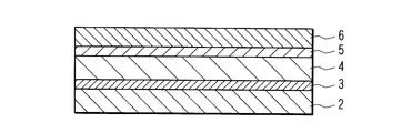
- FIG. 3 is a schematic cross-sectional view of the display panel when viewed from the right side in FIG. 2.
- FIG. 1 is an external perspective view of a liquid crystal display device 100 as a television receiver according to Embodiment 1
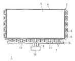
- FIG. 2 is a schematic plan view of a display panel 1 of the liquid crystal display device 100
- FIG. 3 is a right side in FIG. It is typical sectional drawing of the display panel 1 at the time of seeing from. 3, the same parts as those in FIG. 11 are denoted by the same reference numerals.
- the polarizing film attached to the TFT substrate 2 is not shown, but the display member of the present invention applied to the TFT substrate 2 and the CF substrate 4 side as well. It is possible to apply the dividing method.
- the liquid crystal display device 100 includes a display module 11 having a display panel 1 and a backlight unit (not shown), a front cabinet 12 and a rear cabinet 13 made of synthetic resin that are accommodated so as to sandwich the display module 11, and an antenna (not shown). ) Includes a tuner 14 that receives broadcast waves, a decoder 15 that decodes encoded broadcast waves, and a stand 16.
- the display module 11 has a horizontally long and substantially rectangular parallelepiped shape as a whole, and is housed in the front cabinet 12 and the rear cabinet 13 in a vertical posture.
- the display panel 1 includes a TFT substrate 2, a CF substrate 4, a liquid crystal layer 3, and a polarizing film 6.
- the TFT substrate 2 and the CF substrate 4 are bonded to each other with a sealing material interposed therebetween, and a liquid crystal layer 3 is formed by injecting a vertical alignment type liquid crystal material therebetween.
- a dropping bonding method is adopted in which a liquid crystal material is dropped into a frame of a seal pattern of one substrate before being overlapped, and then the other substrate is overlapped and bonded under reduced pressure. You may decide.
- the TFT substrate 2 includes, for example, a TFT (thin film transistor) having a gate electrode, a source electrode, and a drain electrode on an insulating substrate made of glass (hereinafter, not shown), and a plurality of gate wirings (scanning wirings) that supply scanning signals to the TFTs. ) And a plurality of source wirings (signal wirings) for supplying a video signal to the TFT, and a pixel electrode made of, for example, ITO is formed on the surface.
- TFT thin film transistor
- a plurality of gate drivers 8 are arranged on both short sides of the TFT substrate 2, and three source drivers 7 are mounted on the long sides of the TFT substrate 2.
- Two pairs of source substrates 70 are arranged.
- the pair of source substrates 70 and 70 are connected by a connecting portion 71. Ends on the center side of the source substrates 70, 70 near the center are connected to the control substrate 10 via FFC (Flexible Flat Cable) 9, 9.
- FFC Flexible Flat Cable
- the CF substrate 4 is formed by arranging, for example, a black matrix (BM) and color filters such as R (red), G (green), and B (blue) on an insulating substrate made of glass (hereinafter, not shown).
- BM black matrix
- color filters such as R (red), G (green), and B (blue)
- a common electrode made of ITO or the like is formed on the surface.
- the polarizing film 6 is formed by covering both surfaces of an optical film such as a PVA film with a protective film, and is adhered to the side of the CF substrate 4 opposite to the liquid crystal layer 3 side by a curing adhesive 5. As described above, a polarizing film similar to the polarizing film 6 is disposed on the side of the TFT substrate 2 opposite to the liquid crystal layer 3 side, but the illustration is omitted.
- the backlight unit is arranged on the back side of the display panel 1.
- the backlight unit may be either an edge light method (side light method, light guide plate method) or a direct type.
- a gate signal is sent from the gate driver 8 to the gate electrode via the gate wiring, and when the TFT is turned on, the source signal is sent from the source driver 7 via the source wiring. It is sent to the source electrode, and a predetermined charge is written to the pixel electrode through the semiconductor film and the drain electrode.
- a potential difference is generated between each pixel electrode of the TFT substrate 2 and the common electrode of the CF substrate 4, and the liquid crystal layer 3, that is, the liquid crystal capacitance of each pixel and the auxiliary capacitance connected in parallel to the liquid crystal capacitance.
- a predetermined voltage is applied.
- the orientation state of the liquid crystal layer 3 changes depending on the magnitude of the voltage applied to the liquid crystal layer 3, and an image is displayed in a state where the transmittance of the liquid crystal layer 3 is adjusted.
- a defective display area may occur in the display area of the CF substrate 4 of the display panel 1.
- a part to be left in the display area, a part to be left (a lower part of the dividing line a in FIG. 2) and a part to be reproduced (an upper part of the dividing line a in FIG. 2)
- the good display area portion is used for reproduction.
- the source driver 7 and the control substrate 10 be on the display area side where no defective display area exists.
- FIG. 3 is a schematic cross-sectional view for explaining the division of the CF substrate 4 along the division line a in FIG. Along the dividing line a, the polarizing film 6 and the cured adhesive 5 are cut to divide the CF substrate 4, and the right portion in FIG. 3 to be reproduced (the CF substrate 4 having a defective display area, the cured adhesive 5, The part of the polarizing film 6 and the liquid crystal layer 3) is removed leaving the TFT substrate 2 and replaced with a reproduction part.
- Table 1 shows the steps of the method for dividing the display panel 1 according to the present embodiment.
- the ultrasonic cutting roller 20 includes a cutting roller 21, a roller shaft 22, a roller bracket 23, and an oscillation unit 24.
- the roller shaft 22 rotatably supports the cutting roller 21, and the roller bracket 23 supports both ends of the roller shaft 22 in a state where the cutting roller 21 can rotate.
- the oscillating unit 24 includes a piezoelectric element 26 and is attached to the roller bracket 23 with a screw 25.
- the piezoelectric element 26 emits ultrasonic vibration, and the ultrasonic cutting roller 20 vibrates in the direction of the arrow in FIG. 4, that is, in the direction perpendicular to the direction in which the roller bracket 23 holds the roller shaft 22. .
- Examples of the piezoelectric element 26 include those having a frequency of 20 kHz and a vibration amplitude of 50 ⁇ m. In this case, oscillating 50 ⁇ m per second is applied to the object 20,000 times, and by repeating a cycle of shockingly releasing vibration energy to the object at a high speed while the amplitude is small. From a soft synthetic resin film to a hard glass, it can be cut regardless of the material, and the cutting efficiency is also good.
- the cutting roller 21 has a cutting part 21b in which the axial center side of the side surface is recessed and the cutting edges 21a and 21a of the cutting cutter are provided on both end sides of the side surface. With this configuration, the polarizing film 6 that is soft and easily peeled can be discharged from between the blade edges 21a and 21a.
- the cutting part 21b is not limited to the case where the dent in the center part of the side surface and the blade edges 21a and 21a are provided continuously, but may be provided intermittently.
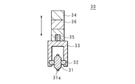
- the cured adhesive 5 and the CF substrate 4 are both hard and easy to break. Since a part of the cured adhesive 5 is vitrified, it can be peeled off by causing breakage starting from the contact portion between the cutting roller and the cured adhesive 5. Therefore, the ultrasonic cutting roller 30 shown in FIG. 5 can also be used.
- the ultrasonic cutting roller 30 includes a cutting roller 31, a roller shaft 32, a roller bracket 33, and an oscillation unit 34.
- the roller shaft 32 rotatably supports the cutting roller 31, and the roller bracket 33 supports both ends of the roller shaft 32 in a state where the cutting roller 31 can rotate.
- the oscillating portion 34 has a built-in piezoelectric element 36 and is attached to the roller bracket 33 by a screw 35.
- the center side of the axial direction of the side surface protrudes from both ends.
- the cutting edge 31a may be provided continuously at the center, or the cutting edge 31a may be provided intermittently in the circumferential direction.
- the cured adhesive 5 can be broken from the central portion.
- the cutting edges 21a and 31a of the ultrasonic cutting rollers 21 and 31 are coated with a carbide material such as titanium nitride (TiN), titanium carbonitride (TiCN), titanium aluminum nitride (TiAlN), aluminum chrome nitride (AlCrN), or the like.
- a carbide material such as titanium nitride (TiN), titanium carbonitride (TiCN), titanium aluminum nitride (TiAlN), aluminum chrome nitride (AlCrN), or the like.
- TiN titanium nitride
- TiCN titanium carbonitride
- TiAlN titanium aluminum nitride
- AlCrN aluminum chrome nitride
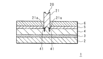
- FIG. 6 is a schematic cross-sectional view showing a state in which the CF substrate 4 is scribed (process (3) in Table 1).
- the ultrasonic cutting roller 20 is used when the base substrate of the CF substrate 4 is glass, the crack 41 can be easily generated at the contact portion as shown in FIG.
- FIG. 7 is a cross-sectional view showing a state (process (4) in Table 1) in which the sealant 17 is applied to the cut portions of the polarizing film 6 and the cured adhesive 5 after scribing the CF substrate 4.
- the sealant 17 an ultraviolet curable resin, a thermosetting resin, or the like is used, and specifically, an epoxy acrylate (trade name “WORD ROCK 700”, manufactured by Kyoritsu Chemical Industry Co., Ltd.) or the like can be given.
- the sealant 17 is applied to the cut portion by a dispenser. As shown in FIG. 7, the applied sealant 17 penetrates into the crack 41 of the CF substrate 4 by capillary action.
- FIG. 8 is a cross-sectional view showing a state (process (5) in Table 1) in which the CF substrate 4 is divided and defective portions are removed. After the CF substrate 4 is divided, the sealant 17 penetrates into the gap due to a pressure difference between the pressure of the gap between the CF substrate 4 and the TFT substrate 2 at the divided portion and the external atmospheric pressure. Therefore, the bubble can be prevented from entering the divided portion.
- the sealing agent 17 is hardened ((6) treatment in Table 1).
- the sealing agent 17 is an ultraviolet curable resin
- the sealing agent 17 is cured by irradiating the sealing agent 17 with ultraviolet rays using a UV irradiator.
- the sealing agent 17 is a thermosetting resin
- the treatment material is carried into a thermosetting furnace, and the sealing agent 17 is thermoset.
- FIG. 9 is a schematic plan view showing the reproduced display panel 1. 9, the same parts as those in FIG. 2 are denoted by the same reference numerals, and detailed description thereof is omitted. In the display panel 1 of FIG. 9, there is no defective portion in the display area.
- FIG. Table 2 below shows a process of dividing the display panel 1 according to the second embodiment.
- the method for dividing the display member according to the second embodiment is the same as the method for dividing the display member according to the first embodiment, except that the ultrasonic cutting blade 40 is used in the process (2) of cutting the cured adhesive 5. It has the composition of.
- FIG. 10 is a cross-sectional view showing the ultrasonic cutting blade 40.
- the ultrasonic cutting sword 40 includes a sword portion 41, a base portion 42, a sword portion bracket 43, and an oscillating portion 44.
- a sword 41 is connected to the base 42, and the sword bracket 43 holds the base 42.
- the oscillating portion 44 incorporates a piezoelectric element 46 and is attached to the sword bracket 43 by screws 45.
- the piezoelectric element 46 generates ultrasonic vibration, and the ultrasonic cutting blade 40 vibrates in the direction of the arrow in FIG. 10, that is, in the direction perpendicular to the direction in which the blade bracket 43 holds the base 42. To do.
- the residue 51 needs to be removed. Occurs.
- the ultrasonic cutting sword 40 when the residue 51 is generated, it can be removed.
- the sword portion 41 in contact with the CF substrate 4 preferably has flexibility.
- the ultrasonic cutting roller 20 or 30 may be used first, and when the residue 51 is generated, the ultrasonic cutting blade 40 may be used.
- the residue when a residue is generated when cutting the adhesive, the residue can be cut out and the substrate can be easily divided.
- FIG. Table 3 below shows a process of dividing the display panel 1 according to the third embodiment.
- the method for dividing the display member according to the third embodiment is the same as that in the embodiment except that the process (3) for scribing the CF substrate 4 and the process (4) for applying the sealant 17 are performed in a reduced pressure environment.
- the display member has the same configuration as that of the display member dividing method according to Embodiment 1.
- the sealing agent 17 since the scribing process is performed on the CF substrate 4 under a reduced pressure environment, air does not enter from the crack 41 of the CF substrate 4 and no bubbles are generated. And after apply
- the present invention is not limited to the contents of Embodiments 1 to 3 described above, and various modifications can be made within the scope of the claims. That is, embodiments obtained by combining technical means appropriately changed within the scope of the claims are also included in the technical scope of the present invention.
- the present invention is not limited to the case where the CF substrate 4 is divided as a substrate.
- the liquid crystal display device of the present invention is not limited to a television receiver. And the dividing method of the display member of this invention is applicable also to display members other than a liquid crystal display device.
Landscapes
- Physics & Mathematics (AREA)
- Nonlinear Science (AREA)
- Optics & Photonics (AREA)
- Crystallography & Structural Chemistry (AREA)
- Chemical & Material Sciences (AREA)
- General Physics & Mathematics (AREA)
- Mathematical Physics (AREA)
- Engineering & Computer Science (AREA)
- Manufacturing & Machinery (AREA)
- Devices For Indicating Variable Information By Combining Individual Elements (AREA)
- Liquid Crystal (AREA)
- Processing Of Stones Or Stones Resemblance Materials (AREA)
- Re-Forming, After-Treatment, Cutting And Transporting Of Glass Products (AREA)
Abstract
良好に、効率良く、残渣がない状態でフィルム及び接着剤を切削して、基板にスクライブ加工を行い、容易に、良好に基板を分断することができる表示部材の分断方法、及び該分断方法により基板を分断する工程を有する液晶 表示装置の製造方法を提供する。表示部材(1)のTFT基板(2)とCF基板(4)とはシール材を挟んで互いに貼り合わされており、その間に液晶が配され、液晶層(3)が形成されている。TFT基板(2)の液晶層(3)と反対側の面には、硬化接着剤(5)により偏光フィルム(6)が貼着されている。超音波により振動する超音波切削ローラ(20)を用いて、偏光フィルム(6)及び硬化接着剤(5)を切削し、CF基板(4)にスクライブ加工を行い、CF基板(4)を分断する。
Description
本発明は、テレビジョン受信機、パーソナルコンピュータ等に備えられる表示部材の分断方法、及び液晶表示装置の製造方法に関する。
表示装置の中で、液晶表示装置は薄型であり、消費電力が低いという特徴を有する。特に、画素毎に薄膜トランジスタ(TFT)等のスイッチング素子を備えるTFT基板を備える液晶表示装置は、高いコントラスト比、及び優れた応答特性を有し、高性能であるため、テレビジョン受信機、パーソナルコンピュータ等に好適に用いられている。
図11は、従来の液晶表示装置の表示パネルを示す模式的断面図である。
表示パネルは、TFT(アクティブマトリクス)基板2、液晶層3、CF基板(カラーフィルタ基板)4、及び偏光フィルム6を備える。
TFT基板2とCF基板4とはシール材を挟んで互いに貼り合わされており、その間に液晶が配され、液晶層3が形成されている。TFT基板2は例えばガラス製の絶縁性基板に画素電極(不図示)を形成してなり、CF基板4は例えばガラス製の絶縁性基板に共通電極(不図示)を形成してなる。偏光フィルム6は、CF基板4の液晶層3と反対側の面に、硬化接着剤5により接着されている。偏光フィルム6は、例えばPVAフィルム等の光学フィルムの両面を保護フィルムで覆ってなる。TFT基板2の液晶層3と反対側の面にも偏光フィルム(不図示)が設けられる。
表示パネルは、TFT(アクティブマトリクス)基板2、液晶層3、CF基板(カラーフィルタ基板)4、及び偏光フィルム6を備える。
TFT基板2とCF基板4とはシール材を挟んで互いに貼り合わされており、その間に液晶が配され、液晶層3が形成されている。TFT基板2は例えばガラス製の絶縁性基板に画素電極(不図示)を形成してなり、CF基板4は例えばガラス製の絶縁性基板に共通電極(不図示)を形成してなる。偏光フィルム6は、CF基板4の液晶層3と反対側の面に、硬化接着剤5により接着されている。偏光フィルム6は、例えばPVAフィルム等の光学フィルムの両面を保護フィルムで覆ってなる。TFT基板2の液晶層3と反対側の面にも偏光フィルム(不図示)が設けられる。
表示パネルの表示領域において、例えばCF基板4に不良部分が生じた場合、不良部分を切断(ハーフカット)して除去し、残った部分を用いて表示パネルを再生することが行われる。
ガラス製の絶縁基板を有するCF基板4上に光学フィルムを有する偏光フィルム6が硬化接着材5により接着されている場合に偏光フィルム6を切断し、CF基板4を分断するとき、以下の問題が生じる。
偏光フィルム6は可撓性を有し、硬化接着剤5による偏光フィルム6とCF基板4との密着性が高く、CF基板4は硬質性を有するため、偏光フィルム6が設けられたCF基板4を分断することが困難である。
図12は、従来の液晶表示装置の表示パネルを示す模式的断面図である。図12に示すように、偏光フィルム6を剥離する際、硬化接着剤5の基板密着性が高いため、硬化接着剤5の残滓51(のこりかす)が発生する。この残滓51が生じた場合、CF基板4を分断することが困難になる。
図12は、従来の液晶表示装置の表示パネルを示す模式的断面図である。図12に示すように、偏光フィルム6を剥離する際、硬化接着剤5の基板密着性が高いため、硬化接着剤5の残滓51(のこりかす)が発生する。この残滓51が生じた場合、CF基板4を分断することが困難になる。
図13は、従来の液晶表示装置の表示パネルを示す模式的断面図である。図13に示すようにCF基板4を分断した場合、分断部分に隙間が生じ、該隙間が減圧状態となっているため、液晶層3に気泡31が生じている。
特許文献1には、夫々表示電極及び引き出し電極が形成された、対向する2枚の樹脂フィルム基板間に液晶材料を挟持した積層基材からなる液晶表示フィルムの切断装置の発明が開示されている。該切断装置は、引き出し電極を露出させるために、露出部分と対応する樹脂フィルム基板を剥離して除去すべく、一方の樹脂フィルム基板のみを切断する切断刃と、切断刃を保持する本体と、切断刃の両側において切断刃と平行に本体に取り付けられたスライド脚部と、スライド脚部の少なくとも一方の脚部を上下動させるねじと、液晶表示フィルムの表面を抑えて切断箇所の平面性を出す抑え手段と、抑え手段に形成したスライド脚部の移動をガイドするガイド部とを備える。
特許文献1の積層基材においては、樹脂フィルム基板に光学フィルムが貼着されていない。また、基板の基材はガラスではなく、合成樹脂であり、ガラス基板に光学フィルムを貼着した表示部材をハーフカットする場合に特許文献1の装置を用いたとしても、光学フィルム及びガラス基板を容易に切削することは困難であり、硬化接着剤の残滓の発生を防止することはできず、基板の分断に係る上述の問題を解決することはできない。
本発明は斯かる事情に鑑みてなされたものであり、良好に、効率良く、残滓がない状態でフィルム及び接着剤を切削して、基板にスクライブ加工を行い、容易に、良好に基板を分断することができる表示部材の分断方法、及び該分断方法により基板を分断する工程を有する液晶表示装置の製造方法を提供することを目的とする。
本発明に係る表示部材の分断方法は、2枚の基板と、少なくとも一方の基板の表面に接着剤により貼着されたフィルムとを備える表示部材の前記基板を分断する表示部材の分断方法において、超音波により振動する切削工具を用いて、前記フィルム及び前記接着剤を切削し、前記基板にスクライブ加工を行い、該基板を分断することを特徴とする。
本発明においては、超音波により振動する切削工具を用いるので、可撓性を有する合成樹脂製材料からガラス等の硬い材料に至るまで、良好に、効率良く切削又はスクライブ加工を行うことができる。
従って、残滓がない状態で接着剤を切削して、容易に、良好に基板を分断することができる。
従って、残滓がない状態で接着剤を切削して、容易に、良好に基板を分断することができる。
本発明に係る表示部材の分断方法は、前記切削工具は、超音波切削ローラであることを特徴とする。
本発明においては、容易に、均一に、前記フィルム及び前記接着剤を切削し、前記基板にスクライブ加工を行うことができる。
本発明に係る表示部材の分断方法は、前記超音波切削ローラは、ローラ側面の軸方向中央側が凹み、該ローラ側面の両端側に切削カッターの刃先が設けられた切削部を備えることを特徴とする。
本発明においては、ローラ側面の凹んだ部分から被切削材の切削片を排出することができる。
本発明に係る表示部材の分断方法は、超音波切削刀を用いて、前記接着剤を切削することを特徴とする。
本発明においては、接着剤を切削する際に残滓が生じた場合に、残滓を切り出すことができ、基板を容易に分断することができる。
本発明に係る表示部材の分断方法は、前記基板にスクライブ加工を行った後、前記フィルム及び前記接着剤の切削部分に封止剤を塗布し、前記基板を分断することを特徴とする。
本発明においては、封止剤が基板のスクライブ加工により生じたクラックに毛細管現象により浸透し、基板を分断した後は、分断部分の基板間の圧力と、外部の大気圧との圧力差により、封止剤が該基板間に浸透し、該基板間への気泡の侵入が防止される。
本発明に係る表示部材の分断方法は、減圧環境下で、前記基板にスクライブ加工を行い、前記封止剤を塗布し、前記基板を分断することを特徴とする。
本発明においては、減圧環境下で基板にスクライブ加工を行うので、基板のクラックから大気が侵入することがなく、気泡が発生しない。そして、減圧環境下で分断部に封止剤を塗布し、大気中に基板を取り出して分断するとき、封止剤がクラックに浸透し、分断完了後は毛細管現象と大気圧とにより基板間に浸透するので、分断処理によって気泡が生じることがない。
本発明に係る表示部材の分断方法は、前記フィルムは、光学フィルムであることを特徴とする。
光学フィルムは可撓性を有するので、切削が困難であるが、本発明においては、超音波により振動する切削工具を用いて切削するので、良好に切削することができる。
本発明に係る液晶表示装置の製造方法は、前記2枚の基板間に液晶層を設けて前記表示部材を製造し、液晶表示装置を製造する液晶表示装置の製造方法において、上述のいずれかの表示部材の分断方法により前記一方の基板を分断して、分断された前記基板の一側を除去し、該一側に対応する部分を再生することを特徴とする。
本発明においては、一方の基板に不良部分が生じた場合に、該基板のハーフカットを良好に行って、良好な表示領域を有する再生品の液晶表示装置を製造することができる。
本発明の表示部材の分断方法によれば、超音波により振動する切削工具を用いて、フィルム及び接着剤を切削し、基板にスクライブ加工を行って基板を分断するように構成されているので、良好に、効率良く、残滓がない状態でフィルム及び接着剤を切削して、基板にスクライブ加工を行い、容易に、良好に基板を分断することができる。
本発明の液晶表示装置の製造方法によれば、本発明の表示部材の分断方法により一方の基板を分断して、分断された基板の一側を除去し、該一側に対応する部分を再生するように構成されているので、一方の基板に不良部分が生じた場合に、基板のハーフカットを良好に行って、良好な表示領域を有する再生品の液晶表示装置を製造することができる。
以下、本発明をその実施の形態を示す図面に基づいて具体的に説明する。
実施の形態1.
図1は実施の形態1に係る、テレビジョン受信機としての液晶表示装置100の外観斜視図、図2は液晶表示装置100の表示パネル1の模式的平面図、図3は図2における右辺側から見た場合の表示パネル1の模式的断面図である。図3中、図11と同一部分は同一符号を付している。以下の実施の形態においては、TFT基板2に貼付されている偏光フィルムの図示を省略しているが、TFT基板2に対しても、CF基板4側に対して適用した、本発明の表示部材の分断方法を適用することが可能である。
液晶表示装置100は、表示パネル1及びバックライトユニット(不図示)を有する表示モジュール11と、該表示モジュール11を挟むようにして収容する合成樹脂製のフロントキャビネット12及びリアキャビネット13と、アンテナ(不図示)から放送波を受信するチューナ14と、符号化された放送波を復号するデコーダ15と、スタンド16とを備える。表示モジュール11は、全体として横長の略直方体状をなし、縦姿勢でフロントキャビネット12及びリアキャビネット13内に収容されている。
実施の形態1.
図1は実施の形態1に係る、テレビジョン受信機としての液晶表示装置100の外観斜視図、図2は液晶表示装置100の表示パネル1の模式的平面図、図3は図2における右辺側から見た場合の表示パネル1の模式的断面図である。図3中、図11と同一部分は同一符号を付している。以下の実施の形態においては、TFT基板2に貼付されている偏光フィルムの図示を省略しているが、TFT基板2に対しても、CF基板4側に対して適用した、本発明の表示部材の分断方法を適用することが可能である。
液晶表示装置100は、表示パネル1及びバックライトユニット(不図示)を有する表示モジュール11と、該表示モジュール11を挟むようにして収容する合成樹脂製のフロントキャビネット12及びリアキャビネット13と、アンテナ(不図示)から放送波を受信するチューナ14と、符号化された放送波を復号するデコーダ15と、スタンド16とを備える。表示モジュール11は、全体として横長の略直方体状をなし、縦姿勢でフロントキャビネット12及びリアキャビネット13内に収容されている。
図3に示すように、表示パネル1は、TFT基板2と、CF基板4と、液晶層3と、偏光フィルム6とを有する。TFT基板2とCF基板4とはシール材を挟んで互いに貼り合わされており、その間に垂直配向型の液晶材料が注入されて液晶層3が形成されている。液晶層3の形成方法として、重ね合わせる前の一方の基板のシールパターンの枠内に液晶材料を滴下し、その後、減圧下で他方の基板を重ね合わせて貼り付ける、滴下貼り合わせ法を採用することにしてもよい。
TFT基板2は、例えばガラス製の絶縁性基板(以下、不図示)に、ゲート電極、ソース電極、及びドレイン電極を有するTFT(薄膜トランジスタ)と、TFTに走査信号を与える複数のゲート配線(走査配線)と、TFTに映像信号を与える複数のソース配線(信号配線)とを形成してなり、表面に例えばITO等からなる画素電極が形成されている。
図2に示すように、TFT基板2の両短辺側には、複数のゲートドライバ8が配されており、TFT基板2の長辺側には、夫々3つのソースドライバ7が実装された、二対のソース基板70が配されている。一対のソース基板70,70は接続部71により接続されている。中央部寄りのソース基板70,70の中央側の端部は、FFC(Flexible Flat Cable)9,9を介し、コントロール基板10に接続されている。
CF基板4は、例えばガラス製の絶縁性基板(以下、不図示)に、ブラックマトリックス(BM)、並びにR(赤)、G(緑)、及びB(青)等のカラーフィルタを配列してなり、表面に例えばITO等からなる共通電極が形成されている。
偏光フィルム6は例えばPVAフィルム等の光学フィルムの両面を保護フィルムで覆ってなり、CF基板4の、液晶層3側と反対の側に硬化接着剤5により接着されている。
上述したように、TFT基板2の、液晶層3側と反対の側にも偏光フィルム6と同様の偏光フィルムが配されるが、図示を省略している。
上述したように、TFT基板2の、液晶層3側と反対の側にも偏光フィルム6と同様の偏光フィルムが配されるが、図示を省略している。
バックライトユニットは、表示パネル1の背面側に配される。バックライトユニットは、エッジライト方式(サイドライト方式、導光板方式)、及び直下型方式のいずれであってもよい。
表示パネル1においては、各画素において、ゲートドライバ8からゲート信号がゲート配線を介してゲート電極に送られ、TFTがオン状態になったときに、ソースドライバ7からソース信号がソース配線を介してソース電極に送られ、半導体膜及びドレイン電極を介して、画素電極に所定の電荷が書き込まれる。このとき、TFT基板2の各画素電極とCF基板4の共通電極との間に電位差が生じ、液晶層3、即ち、各画素の液晶容量、及びその液晶容量に並列に接続された補助容量に所定の電圧が印加される。そして、表示パネル1の各画素において、液晶層3に印加する電圧の大きさによって液晶層3の配向状態が変わり、液晶層3の透過率が調整された状態で画像が表示される。
図2中に示すように、表示パネル1のCF基板4の表示領域中に不良表示領域が生じる場合がある。この場合、図2に示す分断線aに沿って、表示領域のうち、残す部分(図2における分断線aの下側部分)と、再生すべき部分(図2における分断線aの上側部分)とに分断し、良好な表示領域部分は利用して再生する。ここで、良好な表示領域を有する再生品を製造するために、ソースドライバ7及びコントロール基板10が、不良表示領域が存在しない表示領域側にあることが必要である。
図3は、図2の分断線aに沿う、CF基板4の分断を説明するための模式的断面図である。
分断線aに沿って、偏光フィルム6及び硬化接着剤5を切削してCF基板4を分断し、図3における右側の再生すべき部分(不良表示領域を有するCF基板4、硬化接着剤5、偏光フィルム6、及び液晶層3の部分)をTFT基板2を残して除去し、再生部分と置き換える。
下記の表1に、本実施の形態に係る表示パネル1の分断方法の工程を示す。
分断線aに沿って、偏光フィルム6及び硬化接着剤5を切削してCF基板4を分断し、図3における右側の再生すべき部分(不良表示領域を有するCF基板4、硬化接着剤5、偏光フィルム6、及び液晶層3の部分)をTFT基板2を残して除去し、再生部分と置き換える。
下記の表1に、本実施の形態に係る表示パネル1の分断方法の工程を示す。

本実施の形態においては、後述する超音波切削ローラ30を用いて、表1に示す、(1)偏光フィルム6に対する切削処理、(2)硬化接着剤5に対する切削処理、(3)CF基板4に対する基板スクライブ加工(スクライビング)を同時に行う。
図4及び図5は、超音波切削ローラ20を示す模式的断面図である。
超音波切削ローラ20は、切削ローラ21、ローラ軸22、ローラブラケット23、及び発振部24を備える。ローラ軸22は切削ローラ21を回転自在に支持し、ローラブラケット23はローラ軸22の両端を、切削ローラ21が回転できる状態で支持する。発振部24は圧電素子26を内蔵しており、ねじ25によりローラブラケット23に取り付けられている。圧電素子26は超音波振動を発し、該超音波振動により、超音波切削ローラ20は、図4の矢印の方向、即ち、ローラブラケット23がローラ軸22を挟持する方向に垂直な方向に振動する。
超音波切削ローラ20は、切削ローラ21、ローラ軸22、ローラブラケット23、及び発振部24を備える。ローラ軸22は切削ローラ21を回転自在に支持し、ローラブラケット23はローラ軸22の両端を、切削ローラ21が回転できる状態で支持する。発振部24は圧電素子26を内蔵しており、ねじ25によりローラブラケット23に取り付けられている。圧電素子26は超音波振動を発し、該超音波振動により、超音波切削ローラ20は、図4の矢印の方向、即ち、ローラブラケット23がローラ軸22を挟持する方向に垂直な方向に振動する。
圧電素子26として、例えば周波数が20kHzで振動振幅が50μmであるものが挙げられる。この場合、1秒間に50μmの揺動を2万回、対象物に対して与えることになり、振幅が小さいながらも、高速で、振動エネルギーを対象物に衝撃的に放出するサイクルを繰り返すことにより、柔らかい合成樹脂製のフィルムから、硬質のガラスに至るまで材料に関わらず切削することができ、切削効率も良好である。
切削ローラ21は、側面の軸方向中央側が凹み、側面の両端側に切削カッターの刃先21a,21aが設けられた切削部21bを有する。この構成により、柔らかく、剥離しやすい偏光フィルム6を刃先21a,21aの間から排出することができる。切削部21bは、側面の中央部の凹みと、刃先21a,21aとが連続的に設けられる場合に限定されるものではなく、断続的に設けられるものであってもよい。
硬化接着剤5及びCF基板4は共に硬く、割れやすい。硬化接着剤5は一部がガラス化しているため、切削ローラと硬化接着剤5の接触部を起点に破断を起こすことにより、剥離することができる。従って、図5に示す超音波切削ローラ30を用いることもできる。
超音波切削ローラ30は、切削ローラ31、ローラ軸32、ローラブラケット33、及び発振部34を備える。ローラ軸32は切削ローラ31を回転自在に支持し、ローラブラケット33はローラ軸32の両端を、切削ローラ31が回転できる状態で支持する。発振部34は圧電素子36を内蔵しており、ねじ35によりローラブラケット33に取り付けられている。
切削ローラ31は、側面の軸方向の中央側が両端側より突出している。該中央部に刃先31aを連続的に設けてもよく、刃先31aを周方向に断続的に設けることにしてもよい。該中央部を起点に硬化接着剤5の破断を起こすことができる。
切削ローラ31は、側面の軸方向の中央側が両端側より突出している。該中央部に刃先31aを連続的に設けてもよく、刃先31aを周方向に断続的に設けることにしてもよい。該中央部を起点に硬化接着剤5の破断を起こすことができる。
超音波切削ローラ21,31の刃先21a,31aは超硬素材、例えば窒化チタン(TiN)、炭窒化チタン(TiCN)、チタンアルミナイトライド(TiAlN)、アルミクロムナイトライド(AlCrN)等をコートしたもの、ダイヤを焼結したもの等を使用することができる。
図6は、CF基板4にスクライブ加工を行う状態(表1の(3)処理)を示す模式的断面図である。
CF基板4のベース基板がガラスの場合に超音波切削ローラ20を用いたとき、図6に示すように容易に接触部にクラック41を起こすことができる。
CF基板4のベース基板がガラスの場合に超音波切削ローラ20を用いたとき、図6に示すように容易に接触部にクラック41を起こすことができる。
図7は、CF基板4にスクライブ加工を行った後、偏光フィルム6及び硬化接着剤5の切削部分に封止剤17を塗布した状態(表1の(4)処理)を示す断面図である。
封止剤17としては、紫外線硬化性樹脂及び熱硬化性樹脂等が用いられ、具体的には、エポキシアクリレート(商品名「WORLD ROCK 700」、協立化学産業株式会社製)等が挙げられる。封止剤17はディスペンサにより、切削部分に塗布される。
図7に示すように、塗布された封止剤17は、CF基板4のクラック41に、毛細管現象により浸透する。
封止剤17としては、紫外線硬化性樹脂及び熱硬化性樹脂等が用いられ、具体的には、エポキシアクリレート(商品名「WORLD ROCK 700」、協立化学産業株式会社製)等が挙げられる。封止剤17はディスペンサにより、切削部分に塗布される。
図7に示すように、塗布された封止剤17は、CF基板4のクラック41に、毛細管現象により浸透する。
図8は、CF基板4を分断し、不良部分を除去した状態(表1の(5)処理)を示す断面図である。
CF基板4を分断した後は、分断部分のCF基板4とTFT基板2との隙間の圧力と、外部の大気圧との圧力差により、封止剤17が該隙間に浸透する。従って、分断部分への気泡の侵入が防止される。
CF基板4を分断した後は、分断部分のCF基板4とTFT基板2との隙間の圧力と、外部の大気圧との圧力差により、封止剤17が該隙間に浸透する。従って、分断部分への気泡の侵入が防止される。
次に、封止剤17を硬化させる(表1の(6)処理)。
封止剤17が紫外線性硬化樹脂である場合、UV照射機により封止剤17に紫外線を照射して封止剤17を硬化させる。
封止剤17が熱硬化性樹脂である場合、処理材を熱硬化炉内に搬入し、封止剤17を熱硬化させる。
封止剤17が紫外線性硬化樹脂である場合、UV照射機により封止剤17に紫外線を照射して封止剤17を硬化させる。
封止剤17が熱硬化性樹脂である場合、処理材を熱硬化炉内に搬入し、封止剤17を熱硬化させる。
そして、液晶層3、CF基板4、硬化接着剤5、及び偏光フィルム6の不良部分を、TFT基板2を残して除去し、表示パネル1を再生する。ここでは、TFT基板2に対応する偏光フィルムの図示を省略しているが、TFT基板2に偏光フィルムが貼付されている場合においても、本実施の形態に係る方法と同様にしてTFT基板2の分断を行うことができる。
図9は、再生された表示パネル1を示す模式的平面図である。図9中、図2と同一部分は同一符号を付して詳細な説明を省略する。
図9の表示パネル1においては、表示領域に不良部分が存在しない。
図9は、再生された表示パネル1を示す模式的平面図である。図9中、図2と同一部分は同一符号を付して詳細な説明を省略する。
図9の表示パネル1においては、表示領域に不良部分が存在しない。
従来、偏光フィルム6を剥離する際、硬化接着剤5の基板密着性が高いため、図12に示すように硬化接着剤5の残滓51が生じ、CF基板4を分断することが困難であったが、本実施の形態においては、超音波切削ローラ20又は30を用いるので、残滓51の発生が抑制され、かつ容易にCF基板4にスクライブ加工を行うことができ、CF基板4の分断が簡素化されている。
そして、CF基板4の分断前に、上述したように切削部分に封止剤17を塗布するので、分断処理によって気泡が生じることが良好に抑制されている。
そして、CF基板4の分断前に、上述したように切削部分に封止剤17を塗布するので、分断処理によって気泡が生じることが良好に抑制されている。
実施の形態2.
下記の表2に、実施の形態2に係る表示パネル1の分断の工程を示す。
実施の形態2に係る表示部材の分断方法は、硬化接着剤5を切削する処理(2)において、超音波切削刀40を用いること以外は、実施の形態1に係る表示部材の分断方法と同様の構成を有する。
下記の表2に、実施の形態2に係る表示パネル1の分断の工程を示す。
実施の形態2に係る表示部材の分断方法は、硬化接着剤5を切削する処理(2)において、超音波切削刀40を用いること以外は、実施の形態1に係る表示部材の分断方法と同様の構成を有する。
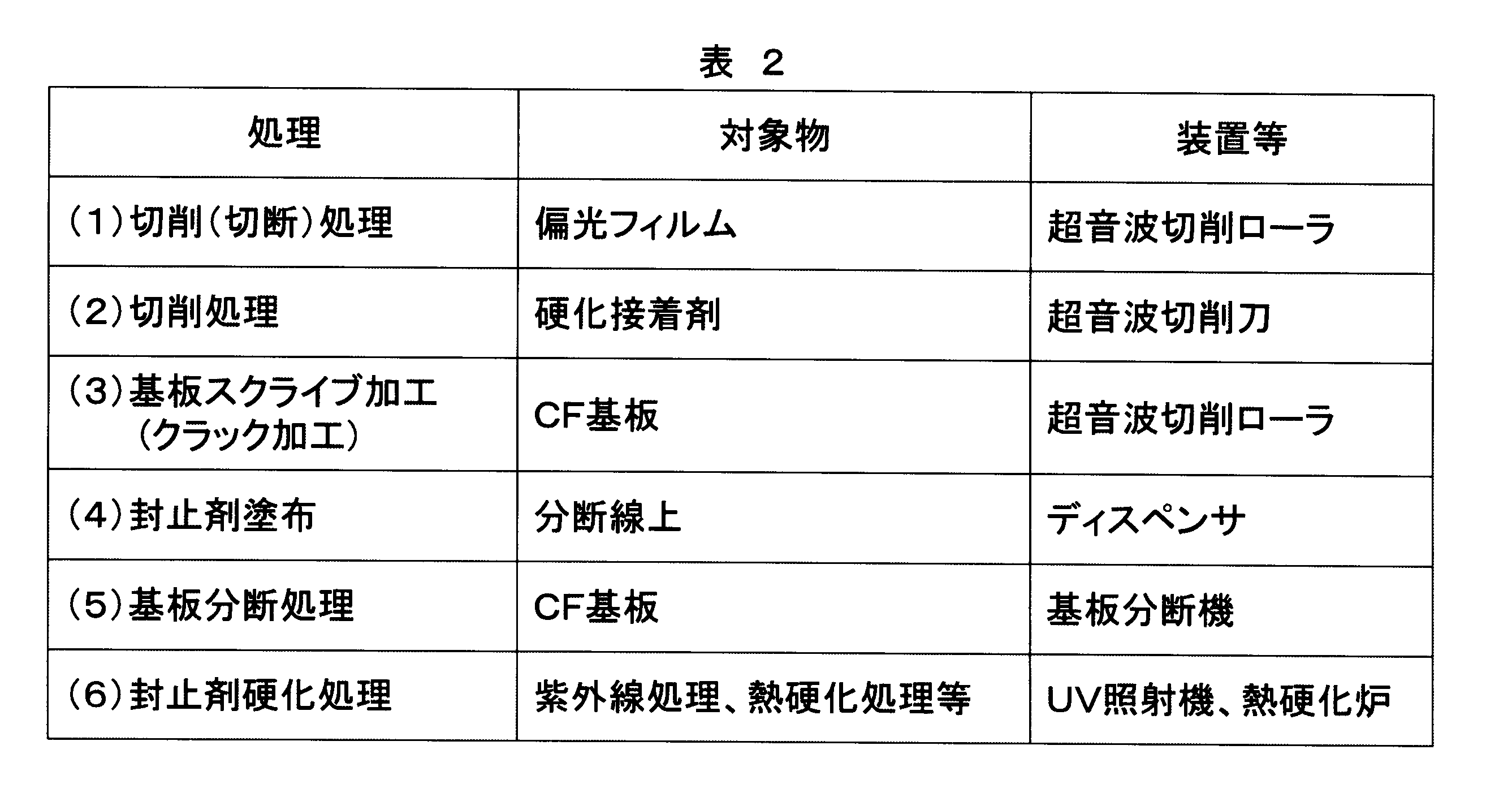
図10は、超音波切削刀40を示す断面図である。
超音波切削刀40は、刀部41、基部42、刀部ブラケット43、及び発振部44を備える。基部42に刀部41が連設されており、刀部ブラケット43は基部42を挟持している。発振部44は圧電素子46を内蔵しており、ねじ45により刀部ブラケット43に取り付けられている。圧電素子46は、超音波振動を発し、該超音波振動により、超音波切削刀40は、図10の矢印の方向、即ち、刀部ブラケット43が基部42を挟持する方向に垂直な方向に振動する。
超音波切削刀40は、刀部41、基部42、刀部ブラケット43、及び発振部44を備える。基部42に刀部41が連設されており、刀部ブラケット43は基部42を挟持している。発振部44は圧電素子46を内蔵しており、ねじ45により刀部ブラケット43に取り付けられている。圧電素子46は、超音波振動を発し、該超音波振動により、超音波切削刀40は、図10の矢印の方向、即ち、刀部ブラケット43が基部42を挟持する方向に垂直な方向に振動する。
図2の分断線aに沿って、偏光フィルム6を切削し、偏光フィルム6が剥離された状態において図12に示すように硬化接着剤5の残滓51が発生した場合、残滓51を除去する必要が生じる。超音波切削刀40を用いることにより、残滓51が生じた場合にこれを除去することができる。残滓51を切り取りやすくするために、CF基板4と接触する刀部41は、柔軟性を有していることが好ましい。
硬化接着剤5を切削する処理(2)において、最初は超音波切削ローラ20又は30を用い、残滓51が生じた場合に、超音波切削刀40を用いることにしてもよい。
硬化接着剤5を切削する処理(2)において、最初は超音波切削ローラ20又は30を用い、残滓51が生じた場合に、超音波切削刀40を用いることにしてもよい。
本実施の形態においては、接着剤を切削する際に残滓が生じたときに、残滓を切り出すことができ、基板を容易に分断することができる。
実施の形態3.
下記の表3に、実施の形態3に係る表示パネル1の分断の工程を示す。
実施の形態3に係る表示部材の分断方法は、CF基板4にスクライブ加工を行う処理(3)、及び封止剤17を塗布する処理(4)を減圧環境下で行うこと以外は、実施の形態1に係る表示部材の分断方法と同様の構成を有する。
下記の表3に、実施の形態3に係る表示パネル1の分断の工程を示す。
実施の形態3に係る表示部材の分断方法は、CF基板4にスクライブ加工を行う処理(3)、及び封止剤17を塗布する処理(4)を減圧環境下で行うこと以外は、実施の形態1に係る表示部材の分断方法と同様の構成を有する。

本実施の形態においては、減圧環境下でCF基板4にスクライブ加工を行うので、CF基板4のクラック41から大気が侵入することがなく、気泡が発生しない。そして、減圧環境下で分断部に封止剤17を塗布した後、大気中にCF基板4を取り出して分断するとき、封止剤17がクラック41に浸透し、分断完了後は毛細管現象と大気圧とにより基板間の液晶層3に浸透するので、分断処理により気泡が生じることがない。
なお、本発明は上述した実施の形態1~3の内容に限定されるものではなく、請求項に示した範囲で種々の変更が可能である。即ち、請求項に示した範囲で適宜変更した技術的手段を組み合わせて得られる実施形態も本発明の技術的範囲に含まれる。
例えば、基板としてCF基板4を分断する場合に限定されるものではない。また、本発明の液晶表示装置はテレビジョン受信機に限定されるものではない。そして、本発明の表示部材の分断方法は、液晶表示装置以外の表示部材にも適用することが可能である。
例えば、基板としてCF基板4を分断する場合に限定されるものではない。また、本発明の液晶表示装置はテレビジョン受信機に限定されるものではない。そして、本発明の表示部材の分断方法は、液晶表示装置以外の表示部材にも適用することが可能である。
1 表示パネル
2 TFT基板
3 液晶層
4 CF基板
5 硬化接着剤
6 偏光フィルム
17 封止剤
20、30 超音波切削ローラ
21、22 切削ローラ
21a、31a 刃先
22、32 ローラ軸
23、33 ローラブラケット
24、34、44 発振部
25、35、45 ねじ
26、36、46 圧電素子
40 超音波切削刀
41 刀部
42 基部
43 刀部ブラケット
100 液晶表示装置
2 TFT基板
3 液晶層
4 CF基板
5 硬化接着剤
6 偏光フィルム
17 封止剤
20、30 超音波切削ローラ
21、22 切削ローラ
21a、31a 刃先
22、32 ローラ軸
23、33 ローラブラケット
24、34、44 発振部
25、35、45 ねじ
26、36、46 圧電素子
40 超音波切削刀
41 刀部
42 基部
43 刀部ブラケット
100 液晶表示装置
Claims (8)
- 2枚の基板と、少なくとも一方の基板の表面に接着剤により貼着されたフィルムとを備える表示部材の前記基板を分断する表示部材の分断方法において、
超音波により振動する切削工具を用いて、前記フィルム及び前記接着剤を切削し、前記基板にスクライブ加工を行い、
該基板を分断することを特徴とする表示部材の分断方法。 - 前記切削工具は、超音波切削ローラであることを特徴とする請求項1に記載の表示部材の分断方法。
- 前記超音波切削ローラは、ローラ側面の軸方向中央側が凹み、該ローラ側面の両端側に切削カッターの刃先が設けられた切削部を備えることを特徴とする請求項2に記載の表示部材の分断方法。
- 超音波切削刀を用いて、前記接着剤を切削することを特徴とする請求項1から3までのいずれか1項に記載の表示部材の分断方法。
- 前記基板にスクライブ加工を行った後、前記フィルム及び前記接着剤の切削部分に封止剤を塗布し、前記基板を分断することを特徴とする請求項1から4までのいずれか1項に記載の表示部材の分断方法。
- 減圧環境下で、前記基板にスクライブ加工を行い、前記封止剤を塗布し、
前記基板を分断することを特徴とする請求項5に記載の表示部材の分断方法。 - 前記フィルムは、光学フィルムであることを特徴とする請求項1から6までのいずれか1項に記載の表示部材の分断方法。
- 前記2枚の基板間に液晶層を設けて前記表示部材を製造し、液晶表示装置を製造する液晶表示装置の製造方法において、
請求項1から7までのいずれか1項に記載の表示部材の分断方法により前記一方の基板を分断して、分断された前記基板の一側を除去し、該一側に対応する部分を再生することを特徴とする液晶表示装置の製造方法。
Priority Applications (4)
| Application Number | Priority Date | Filing Date | Title |
|---|---|---|---|
| JP2017526810A JP6378840B2 (ja) | 2015-07-03 | 2015-07-03 | 表示部材の分断方法、及び液晶表示装置の製造方法 |
| CN201580081204.5A CN107710311A (zh) | 2015-07-03 | 2015-07-03 | 显示构件的截断方法以及液晶显示装置的制造方法 |
| PCT/JP2015/069334 WO2017006405A1 (ja) | 2015-07-03 | 2015-07-03 | 表示部材の分断方法、及び液晶表示装置の製造方法 |
| US15/854,205 US20180136509A1 (en) | 2015-07-03 | 2017-12-26 | Method of dividing display member and method of manufacturing liquid crystal display apparatus |
Applications Claiming Priority (1)
| Application Number | Priority Date | Filing Date | Title |
|---|---|---|---|
| PCT/JP2015/069334 WO2017006405A1 (ja) | 2015-07-03 | 2015-07-03 | 表示部材の分断方法、及び液晶表示装置の製造方法 |
Related Child Applications (1)
| Application Number | Title | Priority Date | Filing Date |
|---|---|---|---|
| US15/854,205 Continuation-In-Part US20180136509A1 (en) | 2015-07-03 | 2017-12-26 | Method of dividing display member and method of manufacturing liquid crystal display apparatus |
Publications (1)
| Publication Number | Publication Date |
|---|---|
| WO2017006405A1 true WO2017006405A1 (ja) | 2017-01-12 |
Family
ID=57686182
Family Applications (1)
| Application Number | Title | Priority Date | Filing Date |
|---|---|---|---|
| PCT/JP2015/069334 Ceased WO2017006405A1 (ja) | 2015-07-03 | 2015-07-03 | 表示部材の分断方法、及び液晶表示装置の製造方法 |
Country Status (4)
| Country | Link |
|---|---|
| US (1) | US20180136509A1 (ja) |
| JP (1) | JP6378840B2 (ja) |
| CN (1) | CN107710311A (ja) |
| WO (1) | WO2017006405A1 (ja) |
Cited By (4)
| Publication number | Priority date | Publication date | Assignee | Title |
|---|---|---|---|---|
| CN107455846A (zh) * | 2017-09-20 | 2017-12-12 | 福建铁工机智能机器人有限公司 | 自动切除鞋底外溢胶水的超声波切割机器人及其使用方法 |
| JPWO2018190181A1 (ja) * | 2017-04-13 | 2019-12-26 | 日東電工株式会社 | 画像表示装置の製造方法および画像表示装置 |
| JPWO2018235462A1 (ja) * | 2017-06-23 | 2020-01-09 | 日東電工株式会社 | 画像表示装置の製造方法および該製造方法により得られた画像表示装置 |
| JP2020021874A (ja) * | 2018-08-02 | 2020-02-06 | 株式会社ディスコ | ウェーハの加工方法 |
Families Citing this family (2)
| Publication number | Priority date | Publication date | Assignee | Title |
|---|---|---|---|---|
| KR20200145881A (ko) | 2019-06-19 | 2020-12-31 | 삼성디스플레이 주식회사 | 표시패널 및 이의 제조 방법 |
| CN114083700B (zh) * | 2021-11-01 | 2024-08-06 | 深圳市高美福商显科技有限公司 | 一种液晶显示面板加工装置及方法 |
Citations (7)
| Publication number | Priority date | Publication date | Assignee | Title |
|---|---|---|---|---|
| JPH03126913A (ja) * | 1989-10-12 | 1991-05-30 | Mitsubishi Electric Corp | 接合基板の分離方法及び液晶表示装置の分離方法 |
| JPH07164400A (ja) * | 1993-12-15 | 1995-06-27 | Nec Corp | ガラス基板の切断装置 |
| JPH07266298A (ja) * | 1994-03-30 | 1995-10-17 | Suzuki Motor Corp | 超音波カッター装置 |
| JP2009160678A (ja) * | 2007-12-28 | 2009-07-23 | Sharp Corp | 切断装置および表示パネルの製造方法 |
| JP2013003299A (ja) * | 2011-06-15 | 2013-01-07 | Takatori Corp | 表示パネルの再生装置及び再生方法 |
| JP2013178394A (ja) * | 2012-02-28 | 2013-09-09 | Nec Saitama Ltd | 表示装置の解体装置及び解体方法 |
| JP2014081486A (ja) * | 2012-10-16 | 2014-05-08 | Japan Display Inc | 液晶表示装置および液晶表示装置の製造方法 |
Family Cites Families (9)
| Publication number | Priority date | Publication date | Assignee | Title |
|---|---|---|---|---|
| JPS5843429A (ja) * | 1981-09-09 | 1983-03-14 | Hitachi Ltd | 液晶表示素子の製造方法 |
| JP2769948B2 (ja) * | 1992-05-20 | 1998-06-25 | キヤノン株式会社 | 液晶パネルユニットの製造方法 |
| JP3413837B2 (ja) * | 1995-11-02 | 2003-06-09 | セイコーエプソン株式会社 | 液晶パネルの製造方法 |
| JP3871983B2 (ja) * | 2002-08-08 | 2007-01-24 | 鹿児島日本電気株式会社 | 液晶表示パネルの製造方法 |
| US8395738B2 (en) * | 2007-10-17 | 2013-03-12 | Japan Display Central Inc. | Liquid crystal display device |
| US8872214B2 (en) * | 2009-10-19 | 2014-10-28 | Sharp Kabushiki Kaisha | Rod-like light-emitting device, method of manufacturing rod-like light-emitting device, backlight, illuminating device, and display device |
| JP2012080460A (ja) * | 2010-10-05 | 2012-04-19 | Seiko Instruments Inc | パッケージの製造方法、圧電振動子、発振器、電子機器および電波時計 |
| KR101956736B1 (ko) * | 2012-03-22 | 2019-03-11 | 엘지디스플레이 주식회사 | 평판표시장치 및 평판표시장치 제조방법 |
| US20150053929A1 (en) * | 2013-08-22 | 2015-02-26 | Board Of Regents. The University Of Texas System | Vertical iii-v nanowire field-effect transistor using nanosphere lithography |
-
2015
- 2015-07-03 WO PCT/JP2015/069334 patent/WO2017006405A1/ja not_active Ceased
- 2015-07-03 JP JP2017526810A patent/JP6378840B2/ja not_active Expired - Fee Related
- 2015-07-03 CN CN201580081204.5A patent/CN107710311A/zh active Pending
-
2017
- 2017-12-26 US US15/854,205 patent/US20180136509A1/en not_active Abandoned
Patent Citations (7)
| Publication number | Priority date | Publication date | Assignee | Title |
|---|---|---|---|---|
| JPH03126913A (ja) * | 1989-10-12 | 1991-05-30 | Mitsubishi Electric Corp | 接合基板の分離方法及び液晶表示装置の分離方法 |
| JPH07164400A (ja) * | 1993-12-15 | 1995-06-27 | Nec Corp | ガラス基板の切断装置 |
| JPH07266298A (ja) * | 1994-03-30 | 1995-10-17 | Suzuki Motor Corp | 超音波カッター装置 |
| JP2009160678A (ja) * | 2007-12-28 | 2009-07-23 | Sharp Corp | 切断装置および表示パネルの製造方法 |
| JP2013003299A (ja) * | 2011-06-15 | 2013-01-07 | Takatori Corp | 表示パネルの再生装置及び再生方法 |
| JP2013178394A (ja) * | 2012-02-28 | 2013-09-09 | Nec Saitama Ltd | 表示装置の解体装置及び解体方法 |
| JP2014081486A (ja) * | 2012-10-16 | 2014-05-08 | Japan Display Inc | 液晶表示装置および液晶表示装置の製造方法 |
Cited By (7)
| Publication number | Priority date | Publication date | Assignee | Title |
|---|---|---|---|---|
| JPWO2018190181A1 (ja) * | 2017-04-13 | 2019-12-26 | 日東電工株式会社 | 画像表示装置の製造方法および画像表示装置 |
| JPWO2018235462A1 (ja) * | 2017-06-23 | 2020-01-09 | 日東電工株式会社 | 画像表示装置の製造方法および該製造方法により得られた画像表示装置 |
| CN107455846A (zh) * | 2017-09-20 | 2017-12-12 | 福建铁工机智能机器人有限公司 | 自动切除鞋底外溢胶水的超声波切割机器人及其使用方法 |
| JP2020021874A (ja) * | 2018-08-02 | 2020-02-06 | 株式会社ディスコ | ウェーハの加工方法 |
| KR20200015420A (ko) * | 2018-08-02 | 2020-02-12 | 가부시기가이샤 디스코 | 웨이퍼의 가공 방법 |
| JP7139050B2 (ja) | 2018-08-02 | 2022-09-20 | 株式会社ディスコ | ウェーハの加工方法 |
| KR102724202B1 (ko) * | 2018-08-02 | 2024-10-30 | 가부시기가이샤 디스코 | 웨이퍼의 가공 방법 |
Also Published As
| Publication number | Publication date |
|---|---|
| JPWO2017006405A1 (ja) | 2018-06-14 |
| CN107710311A (zh) | 2018-02-16 |
| JP6378840B2 (ja) | 2018-08-22 |
| US20180136509A1 (en) | 2018-05-17 |
Similar Documents
| Publication | Publication Date | Title |
|---|---|---|
| JP6378840B2 (ja) | 表示部材の分断方法、及び液晶表示装置の製造方法 | |
| JP2008201629A (ja) | 電気光学装置の製造方法、基板の分断方法、及び、基板分断装置 | |
| US8985177B2 (en) | Polarizing sheet removing tool and removing method | |
| CN103979786A (zh) | 单板玻璃基板的切割方法 | |
| CN108885363B (zh) | 液晶面板的制造方法 | |
| JP2016090855A (ja) | 表示装置およびその製造方法 | |
| JP5285336B2 (ja) | 表示素子の製造方法 | |
| KR100932041B1 (ko) | 편광필름 커팅방법 및 이에 사용되는 편광필름 커팅장치 | |
| JP2010160255A (ja) | 液晶表示装置及びその製造方法 | |
| JP2009205140A (ja) | 電気光学装置の製造方法、及び電気光学装置、並びに電子機器 | |
| JP2008225398A (ja) | 液晶表示素子の製造方法 | |
| JP2005266284A (ja) | 電気光学装置の製造方法、その製造方法で製造した電気光学装置を搭載した電子機器、および偏光板 | |
| JP4999836B2 (ja) | 表示パネルの製造方法 | |
| JP7127566B2 (ja) | 液晶デバイスの製造方法 | |
| JP2004191576A (ja) | フィルムの剥離装置、フィルムの剥離方法及び電気光学装置の製造方法 | |
| KR102633196B1 (ko) | 스크라이빙 장치 및 스크라이빙 방법 | |
| CN101694553A (zh) | 液晶单元、液晶显示设备和形成组件及其制造方法 | |
| CN111025712B (zh) | 液晶显示装置及其制造方法 | |
| CN101372391A (zh) | 基板结构及基板切割方法 | |
| JP2008184358A (ja) | 電気光学装置の製造方法、及び電気光学装置 | |
| JP2007011191A (ja) | 表示装置 | |
| JP2007322693A (ja) | 表示装置の製造方法 | |
| KR20180041588A (ko) | 첩합 기판의 가공 방법 | |
| JP2002023142A (ja) | 液晶表示素子の分断方法及びその分断装置、液晶表示装置及び画像表示応用機器 | |
| JP2009204647A (ja) | 電気光学装置の製造方法 |
Legal Events
| Date | Code | Title | Description |
|---|---|---|---|
| 121 | Ep: the epo has been informed by wipo that ep was designated in this application |
Ref document number: 15897668 Country of ref document: EP Kind code of ref document: A1 |
|
| ENP | Entry into the national phase |
Ref document number: 2017526810 Country of ref document: JP Kind code of ref document: A |
|
| NENP | Non-entry into the national phase |
Ref country code: DE |
|
| 122 | Ep: pct application non-entry in european phase |
Ref document number: 15897668 Country of ref document: EP Kind code of ref document: A1 |