WO2017002528A1 - 半導体装置 - Google Patents
半導体装置 Download PDFInfo
- Publication number
- WO2017002528A1 WO2017002528A1 PCT/JP2016/066528 JP2016066528W WO2017002528A1 WO 2017002528 A1 WO2017002528 A1 WO 2017002528A1 JP 2016066528 W JP2016066528 W JP 2016066528W WO 2017002528 A1 WO2017002528 A1 WO 2017002528A1
- Authority
- WO
- WIPO (PCT)
- Prior art keywords
- resin
- sensor chip
- semiconductor device
- sensor
- cavity
- Prior art date
- Legal status (The legal status is an assumption and is not a legal conclusion. Google has not performed a legal analysis and makes no representation as to the accuracy of the status listed.)
- Ceased
Links
Images








Classifications
-
- B—PERFORMING OPERATIONS; TRANSPORTING
- B81—MICROSTRUCTURAL TECHNOLOGY
- B81B—MICROSTRUCTURAL DEVICES OR SYSTEMS, e.g. MICROMECHANICAL DEVICES
- B81B7/00—Microstructural systems ; Auxiliary parts of microstructural devices or systems
- B81B7/02—Microstructural systems ; Auxiliary parts of microstructural devices or systems containing distinct electrical or optical devices of particular relevance for their function, e.g. microelectro-mechanical systems [MEMS]
-
- G—PHYSICS
- G01—MEASURING; TESTING
- G01C—MEASURING DISTANCES, LEVELS OR BEARINGS; SURVEYING; NAVIGATION; GYROSCOPIC INSTRUMENTS; PHOTOGRAMMETRY OR VIDEOGRAMMETRY
- G01C19/00—Gyroscopes; Turn-sensitive devices using vibrating masses; Turn-sensitive devices without moving masses; Measuring angular rate using gyroscopic effects
- G01C19/56—Turn-sensitive devices using vibrating masses, e.g. vibratory angular rate sensors based on Coriolis forces
- G01C19/5719—Turn-sensitive devices using vibrating masses, e.g. vibratory angular rate sensors based on Coriolis forces using planar vibrating masses driven in a translation vibration along an axis
- G01C19/5769—Manufacturing; Mounting; Housings
-
- G—PHYSICS
- G01—MEASURING; TESTING
- G01P—MEASURING LINEAR OR ANGULAR SPEED, ACCELERATION, DECELERATION, OR SHOCK; INDICATING PRESENCE, ABSENCE, OR DIRECTION, OF MOVEMENT
- G01P15/00—Measuring acceleration; Measuring deceleration; Measuring shock, i.e. sudden change of acceleration
- G01P15/02—Measuring acceleration; Measuring deceleration; Measuring shock, i.e. sudden change of acceleration by making use of inertia forces using solid seismic masses
- G01P15/08—Measuring acceleration; Measuring deceleration; Measuring shock, i.e. sudden change of acceleration by making use of inertia forces using solid seismic masses with conversion into electric or magnetic values
- G01P15/125—Measuring acceleration; Measuring deceleration; Measuring shock, i.e. sudden change of acceleration by making use of inertia forces using solid seismic masses with conversion into electric or magnetic values by capacitive pick-up
-
- H—ELECTRICITY
- H10—SEMICONDUCTOR DEVICES; ELECTRIC SOLID-STATE DEVICES NOT OTHERWISE PROVIDED FOR
- H10D—INORGANIC ELECTRIC SEMICONDUCTOR DEVICES
- H10D48/00—Individual devices not covered by groups H10D1/00 - H10D44/00
- H10D48/50—Devices controlled by mechanical forces, e.g. pressure
-
- H—ELECTRICITY
- H10—SEMICONDUCTOR DEVICES; ELECTRIC SOLID-STATE DEVICES NOT OTHERWISE PROVIDED FOR
- H10W—GENERIC PACKAGES, INTERCONNECTIONS, CONNECTORS OR OTHER CONSTRUCTIONAL DETAILS OF DEVICES COVERED BY CLASS H10
- H10W74/00—Encapsulations, e.g. protective coatings
- H10W74/10—Encapsulations, e.g. protective coatings characterised by their shape or disposition
-
- H—ELECTRICITY
- H10—SEMICONDUCTOR DEVICES; ELECTRIC SOLID-STATE DEVICES NOT OTHERWISE PROVIDED FOR
- H10W—GENERIC PACKAGES, INTERCONNECTIONS, CONNECTORS OR OTHER CONSTRUCTIONAL DETAILS OF DEVICES COVERED BY CLASS H10
- H10W74/00—Encapsulations, e.g. protective coatings
- H10W74/40—Encapsulations, e.g. protective coatings characterised by their materials
-
- H—ELECTRICITY
- H10—SEMICONDUCTOR DEVICES; ELECTRIC SOLID-STATE DEVICES NOT OTHERWISE PROVIDED FOR
- H10W—GENERIC PACKAGES, INTERCONNECTIONS, CONNECTORS OR OTHER CONSTRUCTIONAL DETAILS OF DEVICES COVERED BY CLASS H10
- H10W72/00—Interconnections or connectors in packages
- H10W72/851—Dispositions of multiple connectors or interconnections
- H10W72/874—On different surfaces
- H10W72/884—Die-attach connectors and bond wires
-
- H—ELECTRICITY
- H10—SEMICONDUCTOR DEVICES; ELECTRIC SOLID-STATE DEVICES NOT OTHERWISE PROVIDED FOR
- H10W—GENERIC PACKAGES, INTERCONNECTIONS, CONNECTORS OR OTHER CONSTRUCTIONAL DETAILS OF DEVICES COVERED BY CLASS H10
- H10W74/00—Encapsulations, e.g. protective coatings
-
- H—ELECTRICITY
- H10—SEMICONDUCTOR DEVICES; ELECTRIC SOLID-STATE DEVICES NOT OTHERWISE PROVIDED FOR
- H10W—GENERIC PACKAGES, INTERCONNECTIONS, CONNECTORS OR OTHER CONSTRUCTIONAL DETAILS OF DEVICES COVERED BY CLASS H10
- H10W90/00—Package configurations
- H10W90/701—Package configurations characterised by the relative positions of pads or connectors relative to package parts
- H10W90/731—Package configurations characterised by the relative positions of pads or connectors relative to package parts of die-attach connectors
- H10W90/732—Package configurations characterised by the relative positions of pads or connectors relative to package parts of die-attach connectors between stacked chips
-
- H—ELECTRICITY
- H10—SEMICONDUCTOR DEVICES; ELECTRIC SOLID-STATE DEVICES NOT OTHERWISE PROVIDED FOR
- H10W—GENERIC PACKAGES, INTERCONNECTIONS, CONNECTORS OR OTHER CONSTRUCTIONAL DETAILS OF DEVICES COVERED BY CLASS H10
- H10W90/00—Package configurations
- H10W90/701—Package configurations characterised by the relative positions of pads or connectors relative to package parts
- H10W90/751—Package configurations characterised by the relative positions of pads or connectors relative to package parts of bond wires
- H10W90/752—Package configurations characterised by the relative positions of pads or connectors relative to package parts of bond wires between stacked chips
-
- H—ELECTRICITY
- H10—SEMICONDUCTOR DEVICES; ELECTRIC SOLID-STATE DEVICES NOT OTHERWISE PROVIDED FOR
- H10W—GENERIC PACKAGES, INTERCONNECTIONS, CONNECTORS OR OTHER CONSTRUCTIONAL DETAILS OF DEVICES COVERED BY CLASS H10
- H10W90/00—Package configurations
- H10W90/701—Package configurations characterised by the relative positions of pads or connectors relative to package parts
- H10W90/751—Package configurations characterised by the relative positions of pads or connectors relative to package parts of bond wires
- H10W90/754—Package configurations characterised by the relative positions of pads or connectors relative to package parts of bond wires between a chip and a stacked insulating package substrate, interposer or RDL
Definitions
- the present invention relates to a semiconductor device, in particular, an acceleration / measurement for measuring a motion state of a moving body such as a vehicle such as an automobile or a railway, an airplane, a robot, a construction machine, an agricultural machine, a mobile phone, a smartphone, a tablet, a digital camera, or a video camera.
- a moving body such as a vehicle such as an automobile or a railway, an airplane, a robot, a construction machine, an agricultural machine, a mobile phone, a smartphone, a tablet, a digital camera, or a video camera.
- micro electro mechanical system (MEMS) elements such as digital cameras, video cameras, CCD (Charge u Coupled v Device) image sensor and CMOS (Complementary O Metal Oxide Semiconductor) used for shooting functions of mobile phones, smartphones, tablets, etc., environment recognition for automatic brake control of automobiles, etc. ctor) image sensor or the like of the light receiving element, to a LED (LightEmitting Diode) or a semiconductor laser having a light emitting element or the like.
- MEMS Micro Electro Mechanical Systems
- CCD Charge u Coupled v Device
- CMOS Complementary O Metal Oxide Semiconductor
- sensors having vibrators using MEMS technology have been widely used for the purpose of preventing camera shake of digital cameras and controlling the posture of automobiles and robots.
- this type of vibrator is formed by processing a semiconductor substrate such as silicon or a glass substrate using a MEMS technique such as etching, and is bonded to another substrate in a certain atmosphere and pressure environment.
- a gap is formed and the gap is hermetically sealed.
- Patent Document 1 describes an angular velocity sensor chip and an acceleration sensor chip that are hermetically sealed.
- Patent Document 3 describes an acceleration sensor using a resin package.
- the vibrating body in the chip is hermetically sealed in a gap (hereinafter referred to as a cavity) formed in the sensor chip.
- the cavity is at atmospheric pressure or vacuum.
- a resin for example, when a transfer molding process is applied, when the resin is filled in the mold at a high pressure of about 5 to 20 MPa, a high pressure is also applied to the sensor chip. Because of the large pressure difference between the inside and outside of the sensor, the cavity of the sensor chip is deformed, and if a stress greater than the fracture stress of the material constituting the cavity is applied to the cavity, the cavity breaks and the airtightness inside the cavity is reduced. If the cavity is lost in the direction of the vibrating body and comes into contact with the vibrating body, the vibrating body or the cavity itself may be destroyed.
- Equation 1 The relationship between stress ⁇ and pressure P is expressed by Equation 1. The maximum stress at this time is applied to the end on the long side of the cavity and breaks down at that point.
- the displacement W of the cavity due to the pressure P of the cavity is expressed by Equation 2, and the maximum displacement occurs at the center of the cavity. At this time, even when the pressure does not cause pressure breakdown as described above, if the displacement W exceeds the gap g between the vibrating body and the cavity when there is no load, the cavity comes into contact with the vibrating body. It may destroy itself.
- the substrate on the upper part of the cavity should be thickened.
- a through-wiring is formed in the direction perpendicular to the substrate forming the cavity, and a wire bonding pad is provided above the cavity to perform wire bonding. May be electrically connected to the outside of the sensor chip.
- the through wiring is etched in the vertical direction of the substrate, the element is separated from the etched side wall by an insulator, and a member such as polycrystalline silicon or metal is embedded in the remaining etched portion. Formed with.
- the substrate above the cavity is thickened as a measure for improving the breakdown voltage above the cavity, the electrical characteristics of the through wiring deteriorate, and the sensor performance deteriorates.
- the resistance Rv of the through wiring shown in Equation 3 increases, the thermal noise Vn shown in Equation 4 increases. Considering these problems, it is not easy to increase the thickness of the substrate above the cavity.
- the invention according to claim 1 is a semiconductor device comprising a sensor chip, a first resin covering the inner periphery of the sensor chip, and a second resin covering the outer periphery of the sensor chip. It is characterized by.
- the outer peripheral portion and the inner peripheral portion of the sensor chip are separated from each other, and the outer peripheral portion can be firmly fixed by adopting a transfer mold as usual.
- the mounting state of the sensor chip may change due to a temperature change or a change with time, and a tilt may occur. For example, when the acceleration sensor chip has a tilt ⁇ rad in the detection axis direction, the sensitivity S changes to S ′ as shown in Equation 5, and the zero point Z changes to Z ′ as shown in Equation 6. .
- the sensor chip has a sensing portion, and the first resin covers the first surface of the sensor chip corresponding to the sensing portion, which is the inner peripheral portion, and the second resin.
- the resin is characterized in that it covers the second surface of the sensor chip that does not correspond to the sensing part, which is the outer peripheral part.
- the sensing part can be molded softly by a method such as potting, for example, by molding separately from the outer peripheral part, and the deformation and the destruction of the sensing part can be prevented.
- the thickness h of the upper part of the cavity can be reduced within the allowable pressure resistance range against the above-described deformation and breakage, the cavity substrate itself becomes thinner, and the length t of the through wiring is reduced. Can also be shortened. As a result, the resistance Rv of the through wiring shown in Equation 3 is reduced, so that the thermal noise Vn shown in Equation 4 is reduced, and the performance of the sensor can be improved.
- the invention according to claim 3 is characterized in that the first resin and the second resin are made of the same material.
- the first resin and the second resin are the same, the physical properties such as the linear expansion coefficient and Young's modulus are the same, so the strain generated between the first resin and the second resin. And deformation can be suppressed.
- the invention according to claim 4 is characterized in that the first resin and the second resin are different from each other, and in the invention according to claim 5, the Young's modulus of the first resin is small. It is said. With this structure, it is possible to suppress deformation caused by the first resin, and it is possible to prevent deformation and destruction of the sensing unit.
- the invention according to claim 6 is characterized in that the first resin transmits light. Since this structure allows light to pass through the resin, it can be applied to packaging of light receiving elements and light emitting elements. In addition, since the light is transmitted to the sensing unit, the shape inspection of the sensing unit can be optically performed after sealing. Furthermore, the individual identification of the sensor chip can be optically made possible by marking the individual number of the sensor chip on the surface of the sensing unit.
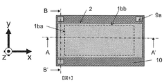
- FIG. 1 is a plan view of an acceleration sensor chip 11 according to a first embodiment of the present invention.
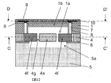
- FIG. 2 is a cross-sectional view taken along the line A-A ′ of FIG. 1.
- FIG. 2 is a sectional view taken along the line B-B ′ of FIG. 1.
- FIG. 3 is a C-C ′ plan view of FIG. 2.
- FIG. 3 is a plan view taken along the line D-D ′ of FIG. 2.
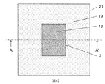
- 1 is a plan view of a chip package 20 according to a first embodiment of the present invention.
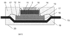
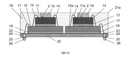
- FIG. 7 is a cross-sectional view taken along the line A-A ′ of FIG. 6. It is a top view of the chip package 21 in the 2nd Example of this invention.
- FIG. 9 is a cross-sectional view taken along the line A-A ′ of FIG. 8. It is a top view of angular velocity sensor chip 11a in the 3rd example of the present invention.
- FIG. 11 is a cross-sectional view taken along the line A-A ′ of FIG. 10.
- FIG. 11 is a sectional view taken along the line B-B ′ of FIG. 10.
- FIG. 12 is a C-C ′ plan view of FIG. 11.
- FIG. 12 is a plan view taken along the line D-D ′ of FIG. 11.
- the number of elements when referring to the number of elements (including the number, numerical value, quantity, range, etc.), especially when clearly indicated, or when clearly limited to a specific number in principle. Except for the specific number, the number may be more or less than the specific number.
- FIG. 1 is a top view of a capacitance detection type acceleration sensor chip 11
- FIG. 2 is a cross-sectional view taken along line AA ′ in FIG. 1
- FIG. 3 is a cross-sectional view taken along line BB ′ in FIG. .
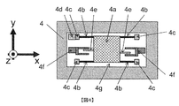
- 4 is a plan view of C-C 'in FIG. 2
- FIG. 5 is a plan view of D-D' in FIG. 6
- FIG. 7 is a cross-sectional view taken along the line A-A 'of FIG.
- the acceleration sensor chip 11 includes a cavity substrate 1, a device substrate 4 on which a vibrating body is formed, and a support substrate 5 that supports the vibrating body.
- the device substrate 4 made of single crystal silicon and the support substrate 5 made of single crystal silicon or glass are bonded together with an insulating film 6 interposed therebetween.
- the cavity 5a may or may not be formed in the support substrate 5 in advance.
- a vibration body is formed by processing the device substrate 4 and the insulating film 6 on these bonded substrates using photolithography and DRIE (Deep Reactive Ion Eching).
- a support beam 4b is connected to a weight 4a that is a vibrating body in a direction orthogonal to the vibration direction of the weight 4a.
- the other ends of these support beams 4b are connected to anchors 4c in the direction orthogonal to the vibration direction.
- the anchor 4c since the anchor 4c is fixed to the support substrate 5 via the insulating film 6, the weight 4a can vibrate in the Y-axis direction.
- a part of the anchor 4c can be electrically connected to a later-described through wiring 7 like the anchor 4d, and is used for electrical connection between the weight 4a side and an external circuit.
- the comb-like detection electrode 4e formed on the device substrate 4 is formed outside the weight 4a.
- a comb-shaped fixed electrode 4f is formed on the device substrate 4 and the insulating film 6 and fixed to the support substrate 5.
- a capacitance C is formed by the distance d between the detection electrode 4e and the fixed electrode 4f, the facing area A, the dielectric constant ⁇ , and the facing number n between the electrodes 4e and 4f.
- the cavity substrate 1 is made of single crystal silicon, and a plurality of through holes for the cavity and the through wiring 7 are formed by using photolithography and DRIE.
- the through wiring 7 is formed by covering the side wall of the through hole with the insulating film 8 and filling the inside with low resistance silicon or a metal material.
- a planar wiring 9 is formed on the surface opposite to the cavity 1a as shown in FIG.
- the planar wiring 9 electrically connects the pad 9a and the through wiring 7 arranged outside the outer periphery of the cavity, and further, in order to protect against corrosion due to scratches and moisture, except for the pad opening 10a, an insulating film 10 covered.
- the cavity substrate 1 configured as described above becomes the acceleration sensor chip 11 by being bonded to the device substrate 4.
- the detection electrode 4e and the fixed electrode 4f formed on the device substrate are electrically connected to the pad 9a on the upper surface of the cavity substrate through the through wiring.
- the effect of damping is obtained by hermetically sealing at atmospheric pressure or vacuum.
- the acceleration sensor chip 11 prepared as described above is assembled into a chip package as shown in FIGS.
- the acceleration sensor chip 11 is mounted on the circuit board 12 via an adhesive 13 and is electrically connected to the circuit board 13 by wire bonding 14.
- the circuit board 12 is mounted on the lead frame 15 via an adhesive 16, and the circuit board 12 and the lead frame 15 are electrically connected by wire bonding 17.
- the chip package 20 is formed by resin sealing.
- the resin sealing first, the second resin 19 is sealed by transfer molding except for the region 2 on the outer periphery of the cavity 1b shown in FIG.
- the region 2 is sealed with a first resin 18 at a low pressure by potting or the like.
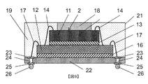
- FIGS. 6 and 7 As a modification of the chip package 20 shown in FIGS. 6 and 7, a chip package 21 will be described with reference to FIGS. The detailed description of the same components as those in FIGS. 6 and 7 will be omitted, and different points will be mainly described below.
- the circuit board 12 is electrically connected to the pads 23 on the board 22 by wire bonding 17.
- the material of the substrate 22 includes ceramics, silicon, alumina, and plastics such as epoxy and glass epoxy.
- the pad 23 is connected to a pad 25 formed on the surface opposite to the pad 23 through a wiring 24 formed on the substrate 22.
- the second resin 19 is sealed except for the region 2 on the surface of the substrate 22 on the pad 23 side.
- the region 2 is sealed with a first resin 18 at a low pressure by potting or the like.
- solder ball 26 may be connected to the pad 25 in order to mount the chip package 21 on a printed board or the like to be electrically connected.
- FIG. 10 is a top view of the capacitance detection type angular velocity sensor chip 11a.
- FIG. 11 is a cross-sectional view taken along line AA 'in FIG. 10
- FIG. 12 is a cross-sectional view taken along line BB' in FIG. .
- 13 is a plan view taken along the line CC ′ of FIG. 11
- FIG. 14 is a plan view taken along the line DD ′ of FIG.
- This structure can be created by the same method as the structure shown in FIGS. 1 to 9, but the structure of the vibrating body created by the device substrate 4 is different.
- FIGS. 10 to 14 detailed description of the same components as those of FIGS. 1 to 9 will be omitted, and different points will be mainly described.
- a device substrate 4 on which a vibrating body to be described later is formed is bonded to the cavity substrate 1 and the support substrate 5 to form a hollow structure and hermetically sealed in a vacuum or air. It is characterized by its configuration. Then, the angular velocity sensor chip 11a is connected to the circuit board 12a for the angular velocity sensor, and is assembled in the form of the chip package 20 or the chip package 21 as in FIG. 6, FIG. 7, FIG. 8, or FIG.
- the left vibrator 4q1 and the right vibrator 4q2 are arranged symmetrically with respect to each other and are connected to each other via a link beam 4p.
- the portions formed only by the device substrate 4 are both movable with respect to the support substrate 5 via the anchor 4c and the insulating film 6, and the natural frequencies of the vibrators 4q1 and 4q2 are designed to be equal. .
- a weight 4h that is a first vibrating body is formed, and a support beam 4i is connected in a direction orthogonal to the driving direction of the vibrating body.
- the other ends of the support beams 4i are connected to the anchors 4c in the direction orthogonal to the driving direction.
- the weight 4h, which is the first vibrating body can vibrate in the X-axis direction by the support beam 4i.
- a part of the anchor 4c can be electrically connected to the above-described through wiring 7 like the anchor 4d, and is used for electrical connection between the vibrating body side and the external circuit.
- the comb-like drive electrode 4l formed on the device substrate 4 is formed outside the weight 4h which is the first vibrating body.
- a comb-shaped drive electrode 4 m is formed on the device substrate 4 and the insulating film 6 and fixed to the support substrate 5.
- the drive electrode 4m is electrically connected to the pad 9a via the through wiring 8 and the planar wiring 9 on the cavity substrate, and is connected to an external oscillation circuit. A predetermined frequency signal is transmitted to the drive electrode 4m. When applied, an electrostatic force is generated between the electrodes 4l and 4m, and the weight 4h as the first vibrating body vibrates in the X-axis direction.
- the weight 4 j that is the second vibrating body is formed inside the weight 4 h that is the first vibrating body, and for detection that extends above and below the weight 4 j in the same direction as the vibration direction of the weight 4 h.
- the other end of the beam 4k is connected to a weight 4h that is a first vibrating body.
- the weight 4j, which is the second vibrating body is movable as viewed from the support substrate 5, vibrates in conjunction with the weight 4h, which is the first vibrating body, by the detection beam 4k, and is orthogonal to the X axis. Vibration is possible in the Y-axis direction.
- a comb-like detection electrode 4n is provided on the device substrate 4 adjacent to the weight 4j.
- a comb-like detection 4o is provided at a position facing the detection electrode 4n.
- the detection electrode 4 o is formed on the device substrate 4 and the insulating film 6 and is fixed to the support substrate 5.
- the detection electrode 4o is electrically connected to the pad 9a via the through wiring 8 and the planar wiring 9 on the cavity substrate, and then connected to an external signal processing circuit.
- the weight 4h and the weight 4j have the natural frequency fx. Vibrates in the X-axis direction.
- the weight 4j vibrates in the Y-axis direction at the natural frequency fy.
- the angular velocity sensor according to the embodiment of the present invention operates as follows.
- the left vibrator 4q1 and the right vibrator 4q2 generate an electrostatic force between the electrodes 4m and 4l by applying an alternating voltage of frequency f to the drive electrode 4m in FIG.
- the weight 4h which is the first vibrating body, is vibrated in the X-axis direction.
- the weight 4j as the second vibrating body vibrates in conjunction with the weight 4h in the X-axis direction.
- the relationship between the displacement x of the weight 4h in the X-axis direction and the velocity v thereof is expressed by Equation 8.
- the weight 4j which is the second vibrating body vibrates in the Y-axis direction by the Coriolis force Fc expressed by Equation 9, and the capacitance between the detection electrodes 4n and 4o changes. By detecting this change in capacitance, the angular velocity ⁇ around the Z axis can be detected.
- the capacitance change between the detection electrodes 4n and 4o that is, the displacement amount of the weight 4j in the Y-axis direction becomes zero.
- the voltage applied between the electrodes 4n and 4o may be servo-controlled, and the Coriolis force Fc may be obtained from the applied voltage.
- the left vibrator 4q1 and the right vibrator 4q2 arranged so as to be symmetric with each other are provided such that the vibrator 4q1 and the vibrator 4q2 drive and vibrate in mutually opposite phases, thereby increasing the acceleration from the outside. While canceling, there is an advantage that the detection signal of the angular velocity can be detected with high sensitivity as an addition from the two vibrators, and the vibration of the vibrator can be hardly leaked to the outside.
- a composite sensor will be described as a fourth embodiment of the structure of the present invention.
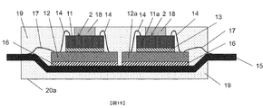
- the composite sensor is a sensor in which a plurality of sensors such as the acceleration sensor and the angular velocity sensor are combined in one package.
- the lead frame 15 or the substrate 22 is one.
- FIGS. 15 and 16 the detailed description of the same components as those in FIGS. 6 to 9 will be omitted, and the differences will be mainly described.
- FIG. 15 shows a chip package 20a as a modification of FIG. 7, and FIG. 16 shows a chip package 21a as a modification of FIG.
- the combination of the composite sensors is not limited to only one acceleration sensor and one angular velocity sensor, and may be the same type of sensor or different types of sensors, and two or more sensors may be used. It only has to be configured.
- circuit board 12b for a composite sensor is characterized in that circuit boards for a plurality of sensors are formed on one board.
- FIGS. 17 and 18 detailed description of the same components as those of FIGS. 6, 7, 8, 9, 15, and 16 is omitted. I will explain.
- FIG. 17 shows a chip package 20b as a modification of FIG. 7
- FIG. 18 shows a chip package 21b as a modification of FIG.
- the combination of sensor chips in the composite sensor is not limited to one acceleration sensor chip 11 and one angular velocity sensor chip 11a, but may be a combination of different types of sensor chips, even if the same type of sensor chip is combined. Either may be sufficient, and it is sufficient that the sensor chip is composed of two or more.
- This structure can be created by the same method as the structure shown in FIGS. 1 to 14, but the structure of the vibrating body created by the device substrate 4 is different.
- FIG. 19 the same components as those of FIGS. 1 to 14 will not be described in detail, and different points will be mainly described.
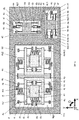
- a first acceleration sensing unit 40 that detects acceleration in the X-axis direction, and the first acceleration sensing unit that is orthogonal to the first acceleration sensing unit on the XY plane
- a combination of a second acceleration sensing unit 41 that detects acceleration and an angular velocity sensing unit 50 that is arranged on the XY plane and detects an angular velocity around the Z axis is formed on the device substrate 4 shown in FIGS. 4 and 13.
- a modification of the vibrating body structure is shown in FIG.
- the cavity 4g1 of the first acceleration sensing unit 40 and the cavity 4g2 of the second acceleration sensing unit 41 may be connected to each other or independent. Further, the cavity 4g3 of the angular velocity sensing unit may be connected to or independent from each of the cavities 4g1 and 4g2. Further, as described above, in each of the sensing units 40, 41, and 50, the anchors 4d1, 4d2, and 4d3 are respectively used as electrodes for electrical connection between the vibrating body side and the external circuit board 12b. Provided. At this time, the anchors 4d1, 4d2, and 4d3 are electrically connected to the pads 9a on the surface of the cavity substrate through the through wirings 7. The pad 9a is electrically connected to the circuit board 12b via the wire bonding 14.
- the above-described sensor chip 11b is connected to the circuit board 12b through the wire bonding 14, and is assembled in the form of the chip package 21 or the chip package 22 as in FIG. 6, FIG. 7, FIG. 8, or FIG.
- the present invention may be applied to a MEMS element having a cavity, an imaging element, a light emitting element, and the like, and a first covering the inner peripheral part (sensing part) of the sensor chip. And a second resin covering the outer periphery of the sensor chip, the sensor chip is firmly fixed with the first resin and the sensing part is covered with the second resin.
- the sensing unit can be protected.
Landscapes
- Physics & Mathematics (AREA)
- General Physics & Mathematics (AREA)
- Engineering & Computer Science (AREA)
- Manufacturing & Machinery (AREA)
- Radar, Positioning & Navigation (AREA)
- Remote Sensing (AREA)
- Computer Hardware Design (AREA)
- Microelectronics & Electronic Packaging (AREA)
- Pressure Sensors (AREA)
- Gyroscopes (AREA)
Abstract
本発明の目的はセンサチップの破損を抑止しつつ、センサチップの固定を図ることである。その結果、歩留まりを向上した半導体装置を提供することを目的とする センサチップと,前記センサチップの内周部を覆った第一の樹脂と,前記センサチップの外周部を覆った第二の樹脂とを備えた半導体装置であり、前記センサチップはセンシング部を有し,前記センシング部は前記センサチップの内周部にあり,前記第一の樹脂は前記センシング部に対応する前記センサチップの第一表面を覆い,前記第二の樹脂は前記センシング部に対応しない前記センサチップの第二表面を覆ったことを特徴とする半導体装置である。
Description
本発明は半導体装置に関し,特に,自動車,鉄道等の車両,飛行機,ロボット,建設機械,農業機械,携帯電話,スマートフォン,タブレット,デジタルカメラ,ビデオカメラ等の運動体の運動状態を測定する加速度・角速度センサなどの慣性センサや,フィルタ,クロック発生用の振動子等,構造体が気密に封止された微小電気機械システム(MEMS(Micro Electro Mechanical Systems))素子の他,デジタルカメラ,ビデオカメラ,携帯電話,スマートフォン,タブレット等の撮影機能や,自動車の自動ブレーキ制御用の環境認識等に使用される,CCD(Charge Coupled Device)撮像素子やCMOS(Complementary MetalOxide Semiconductor)撮像素子等の受光素子,LED(LightEmitting Diode)や半導体レーザ等の発光素子等に関するものである。
近年,デジタルカメラの手ブレ防止,自動車やロボット等の姿勢制御などを目的にして,MEMS技術を用いた振動子を有するセンサが幅広く用いられるようになってきている。
一般的に,この種の振動子はシリコン等の半導体基板やガラス基板等をエッチング等のMEMS技術を用いて加工することにより形成され,一定の雰囲気,圧力環境下で別の基板を張り合わせることにより,空隙を形成し,空隙は気密封止されている。例えば,特許文献1には気密封止した角速度センサチップと加速度センサチップが記載されている。
また,デジタルカメラやスマートフォン等に用いられている受光素子としては,例えば,特許文献2記載のように,凹部を有するセラミックのパッケージとカバー部材とを用いて,ウエハから個片化された撮像素子のチップを内部に封止する構成が知られている。
これらの素子のパッケージ構造として,樹脂パッケージが着目されている。樹脂パッケージは,従来のセラミクスパッケージよりも,量産性が高く,製造コストを低減する上で有効なパッケージ形態である。例えば,特許文献3には樹脂パッケージを用いた加速度センサが記載されている。
ところで,上述した従来技術において,チップにおける振動体は,センサチップ内に形成した空隙部(以下,キャビティ)に気密封止されている。また,キャビティ内は,大気圧又は真空となっている。このようなセンサチップを樹脂パッケージする場合において,例えばトランスファモールド工程を適用すると,樹脂を5~20MPa程度の高圧で金型中に充填する際,センサチップに対しても高圧が印加され,センサチップの内外圧力差が大きい為に,センサチップのキャビティが変形し,キャビティに対してキャビティを構成する材料が持つ破壊応力以上の応力が印加された場合,キャビティが破壊し,キャビティ内の気密性が失われる,また,キャビティが振動体の方向に陥没し,振動体に接触する場合,振動体やキャビティ自体を破壊する場合がある。
応力σと圧力Pの関係は数1によって表される。この時の最大応力はキャビティ長辺側の端部に印加され,その箇所で耐圧破壊する。
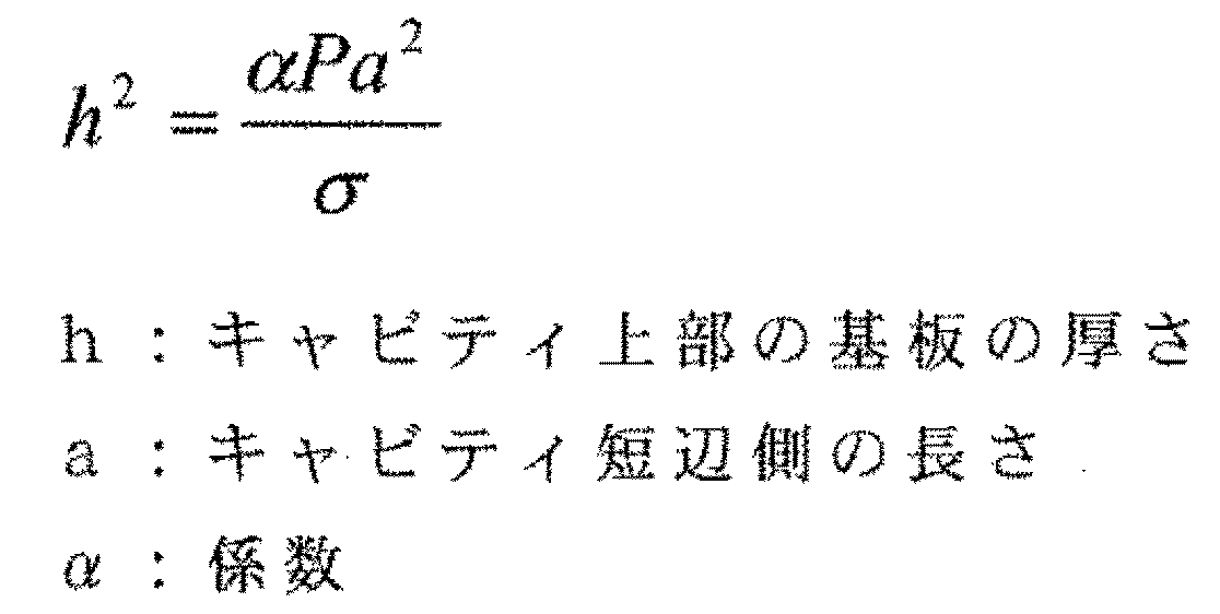
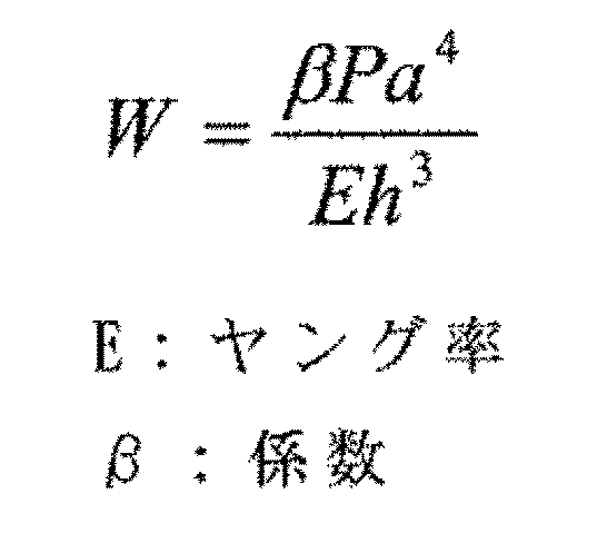
更に,前記キャビティの圧力Pによるキャビティの変位Wは数2によって表され,最大変位はキャビティ中心部で発生する。このとき,前述のように耐圧破壊しない圧力下であっても,無負荷時における前記振動体と前記キャビティ間ギャップgを変位Wが上回ると,キャビティが振動体と接触するため,振動体やキャビティ自体を破壊する場合がある。
キャビティ上部において,耐圧向上や変位低減をするには,キャビティ上部の基板を厚くすれば良いのは明らかである。しかしながら,振動体とセンサチップ外部との間で,電気信号を入出力する場合,キャビティを形成している基板の垂直方向に貫通配線を形成し,キャビティ上部にワイヤボンディング用のパッドを設けワイヤボンディングによりセンサチップ外部と電気的に接続する場合がある。その際,貫通配線は,基板の垂直方向にエッチングを行い,エッチングした側壁に対して絶縁体により素子分離をした上で,残りのエッチング部に対して多結晶シリコンや金属等の部材を埋め込むことで形成される。このとき,キャビティ上部の耐圧向上の対策として,キャビティ上部の基板を厚くした場合,貫通配線の電気特性が悪化するために,センサの性能が悪化する。例えば,数3に示している貫通配線の抵抗Rvが増加するため,数4に示している熱雑音Vnが増加する。これらの問題を考慮すると,キャビティ上部の基板を厚くするのは容易ではない。


上述した課題を解決するためには,前記キャビティ上部に圧力をかけずに樹脂パッケージすることが有効である。それにより,数1及び数2で示しているキャビティ上部や振動体の破壊を防ぐことができる。
上記の目的を達成するため,本願において開示される発明のうち,代表的なものによって得られる効果を簡単に説明すれば以下のとおりである。
請求項1記載の発明では,センサチップと,前記センサチップの内周部を覆った第一の樹脂と,前記センサチップの外周部を覆った第二の樹脂とを備えた半導体装置であることを特徴としている。本発明では,センサチップの外周部と内周部の樹脂を分けることで,外周部は,従来通りトランスファモールドを採用することで,強固に固定することができる。一方,外周部が強固に固定できない場合は,センサチップの実装状態が温度変化や経時変化により変化し,傾きが発生する可能性がある。例えば,加速度センサチップが検出軸方向に傾きφradが発生した場合,感度Sは数5で示すようにS´に変化し,ゼロ点Zは数6で示すようにZ´に変化する問題がある。
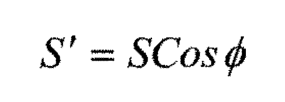
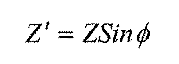
請求項2記載の発明では,センサチップはセンシング部を有し,前記第一の樹脂は,前記内周部である,前記センシング部に対応する前記センサチップの第一表面を覆い,前記第二の樹脂は,前記外周部である,前記センシング部に対応しない前記センサチップの第二表面を覆ったことを特徴としている。
前記センシング部に空隙を有している場合,前記センシング部を外周部と同じく強固にモールドすると,センシング部に変形や破壊が発生する問題がある。本発明では,センシング部は,外周部とは別にモールドすることにより,例えばポッティング等の方式で柔らかくモールドすることが出来,センシング部の変形の抑制や破壊を防止することが出来る。
更に,前述の変形や破壊に対して許容できる耐圧力範囲内において,前記キャビティ上部の厚さhは薄くすることもできるようになるため,キャビティ基板自体が薄くなり,前記貫通配線の長さtも短くすることができる。それにより,数3に示している貫通配線の抵抗Rvが低くなることで,数4に示す熱雑音Vnが低くなり,センサの性能を向上することができる。
請求項3記載の発明では,第一の樹脂と第二の樹脂が同一の材質であることを特徴としている。本構造により,第一の樹脂と第二の樹脂が同一であるために,線膨張係数やヤング率等の物性値が同一になるため,第一の樹脂と第二の樹脂間で発生する歪や変形を抑えることができる。
請求項4記載の発明では,第一の樹脂と第二の樹脂が互いに異なる材質であることを特徴とし,更に,請求項5記載の発明では,第一の樹脂のヤング率が小さいことを特徴としている。本構造により,第一の樹脂で生じる変形を抑えることができ,前記センシング部の変形の抑制や破壊を防止することが出来る。
また,請求項6記載の発明では,第一の樹脂は光を透過することを特徴としている。本構造により,光が樹脂を透過するため,受光素子や発光素子のパッケージングに適用できる。また,センシング部まで光が透過するため,封止後にセンシング部の形状検査が光学的に可能になる。更に,センシング部表面にセンサチップの個別番号を刻印しておくことで,センサチップの個別確認も光学的に可能になる。
以下の実施の形態においては便宜上その必要があるときは,複数のセクションまたは実施の形態に分割して説明するが,特に明示した場合を除き,それらはお互いに無関係なものではなく,一方は他方の一部または全部の変形例,詳細,補足説明等の関係にある。
また,以下の実施の形態において,要素の数等(個数,数値,量,範囲等を含む)に言及する場合,特に明示した場合および原理的に明らかに特定の数に限定される場合等を除き,その特定の数に限定されるものではなく,特定の数以上でも以下でもよい。
さらに,以下の実施の形態において,その構成要素(要素ステップ等も含む)は,特に明示した場合および原理的に明らかに必須であると考えられる場合等を除き,必ずしも必須のものではないことは言うまでもない。
同様に,以下の実施の形態において,構成要素等の形状,位置関係等に言及するときは,特に明示した場合および原理的に明らかにそうではないと考えられる場合等を除き,実質的にその形状等に近似または類似するもの等を含むものとする。このことは,上記数値および範囲についても同様である。
また,実施の形態を説明するための全図において,同一の部材には原則として同一の符号を付し,その繰り返しの説明は省略する。なお,図面をわかりやすくするために平面図であってもハッチングを付す場合がある。
(実施の形態1)
本発明の構造第1の実施例として,MEMS型加速度センサを用いて発明を説明する。
本発明の構造第1の実施例として,MEMS型加速度センサを用いて発明を説明する。
図1は静電容量検出型の加速度センサチップ11の上面図であり,図2は図1のA-A’の断面図,図3は図1のB-B’の断面図を示している。また,図4は図2のC-C’の平面図,図5は図2のD-D’の平面図を示している。そして,図6は前記加速度センサチップ11のチップパッケージ19における平面図,図7は図6のA-A’断面図を示している。
加速度センサチップ11は,キャビティ基板1と振動体を形成したデバイス基板4と,振動体を支持する支持基板5とで構成される。
まず,振動体の形成において,単結晶シリコンからなるデバイス基板4と単結晶シリコンもしくはガラスからなる支持基板5とを絶縁膜6を介して張り合わせる。この際,支持基板5には予めキャビティ5aを形成しておいても良いし,なくても良い。次に,これらの張り合わせた基板をフォトリソグラフィとDRIE(Deep Reactive Ion Etching)を用いて,デバイス基板4と絶縁膜6を加工することで振動体を形成する。
デバイス基板4に形成した振動体において,図4に示すように,振動体である錘4aには,錘4aの振動方向とは直交する方向に支持梁4bが接続される。これらの支持梁4bの他方の端部は,それぞれ振動方向と直交した方向にあるアンカー4cと接続される。このとき,アンカー4cは絶縁膜6を介して支持基板5に固定されているため,錘4aはY軸方向に振動可能になる。また,アンカー4cの一部は,アンカー4dのように後述する貫通配線7と電気的に接続可能となっており,錘4a側と外部回路間との電気的接続に使用される。
デバイス基板4に形成された櫛歯状の検出電極4eは,錘4aの外側に形成される。櫛歯状の検出電極4eに対向して,櫛歯状の固定電極4fがデバイス基板4と絶縁膜6上に形成され,支持基板5に対して固定される。そして,数7で示すように,検出電極4eと固定電極4f間の距離dと対向面積Aと誘電率ε,電極4e,4f間の対向数nとで静電容量Cを形成する。そして,振動体にy軸方向に加速度が印加されると,可動体である錘4aはy軸方向に変位し,この時の電極間の変位量Δyが静電容量変化ΔCとなる。

次に,キャビティ基板1においては,単結晶シリコンからなり,フォトリソグラフィとDRIEを用いることでキャビティと貫通配線7のための複数の貫通孔を形成する。そして,貫通配線7は,貫通孔の側壁を絶縁膜8で覆った上で,内側を低抵抗シリコンもしくは金属材料により埋め込んで形成する。そして,キャビティ1aと反対の面に,図5に示すように,平面配線9を形成する。平面配線9は,キャビティの外周よりも外側に配置したパッド9aと貫通配線7とをそれぞれ電気的に接続し,更に傷や水分による腐食に対する保護のため,パッド開口部10aを除いて,絶縁膜10で覆われる。
以上で構成されるキャビティ基板1はデバイス基板4と張り合わせることで加速度センサチップ11になる。この時,デバイス基板上に形成した検出電極4e,固定電極4fは貫通配線を介して,キャビティ基板上面のパッド9aに電気的に接続される。なお,張り合わせの際は,大気圧もしくは真空にて気密封止することで,ダンピングの効果を得ている。
前述の通り作成された加速度センサチップ11は,図6,図7に示すようにチップパッケージに組み立てられる。加速度センサチップ11は,回路基板12上に接着材13を介して実装され,ワイヤボンディング14により,回路基板13と電気的に接続される。そして,回路基板12はリードフレーム上15に接着材16を介して実装し,回路基板12とリードフレーム15はワイヤボンディング17により電気的に接続される。
次に,樹脂封止によりチップパッケージ20となる。樹脂封止においては,先ず,図1に示した前記キャビティ部1b外周の領域2を除いて,第二の樹脂19にてトランスファモールドにより封止する。次に,前記領域2を第一樹脂18にてポッティング等により低圧で封止する。本構造により,モールド圧力によるキャビティ上部の変形抑制や破壊防止をすることができる。
(実施の形態2)
本発明の構造第2の実施例として,チップパッケージの変形例について述べる。
本発明の構造第2の実施例として,チップパッケージの変形例について述べる。
図6,図7に示すチップパッケージ20の変形例として,チップパッケージ21について,図8,図9を参照しつつ説明する。なお,図6,図7と同一の構成要素については,その詳細な説明を省略し,以下,異なる点を中心に説明することとする。
チップパッケージ21において,回路基板12は基板22上のパッド23にワイヤボンディング17により電気的に接続される。このとき,基板22の材質はセラミクスやシリコン,アルミナの他,エポキシ,ガラスエポキシ等のプラスチック等が挙げられる。そして,パッド23は基板22に形成された配線24を介して,パッド23とは反対の面に形成されたパッド25に接続される。
次に,樹脂封止において,第二の樹脂19は,基板22のパッド23側の面において,領域2を除いて封止する。次に,前記領域2を第一樹脂18にてポッティング等により低圧で封止する。本構造により,モールド圧力によるキャビティ上部の変形抑制や破壊防止をすることができる。
なお,チップパッケージ21をプリント基板等に実装して電気的に接続するために,パッド25には半田ボール26を接続しても良い。
(実施の形態3)
以下,本発明の構造第3の実施例としてMEMS型角速度センサについて述べる。
図10は静電容量検出型の角速度センサチップ11aの上面図であり,図11は図10のA-A’の断面図,図12は図10のB-B’の断面図を示している。また,図13は図11のC-C’の平面図,図14は図11のD-D’の平面図を示している。本構造は,図1乃至図9に示した構造と同様の手法で作成できるが,デバイス基板4で作成する振動体の構造が異なる。以下,図10乃至図14を説明するに当たり,図1乃至図9と同一の構成要素については,その詳細な説明を省略し,異なる点を中心に説明することとする。
以下,本発明の構造第3の実施例としてMEMS型角速度センサについて述べる。
図10は静電容量検出型の角速度センサチップ11aの上面図であり,図11は図10のA-A’の断面図,図12は図10のB-B’の断面図を示している。また,図13は図11のC-C’の平面図,図14は図11のD-D’の平面図を示している。本構造は,図1乃至図9に示した構造と同様の手法で作成できるが,デバイス基板4で作成する振動体の構造が異なる。以下,図10乃至図14を説明するに当たり,図1乃至図9と同一の構成要素については,その詳細な説明を省略し,異なる点を中心に説明することとする。
角速度センサチップ11aの構造において,後述する振動体を形成したデバイス基板4は,キャビティ基板1と支持基板5とで張り合わせることで,中空構造とし,且つ真空もしくは大気にて気密に封止された構成であることを特徴としている。そして,角速度センサチップ11aは,角速度センサ用の回路基板12aに接続され,図6,図7もしくは図8,図9と同様に,チップパッケージ20もしくはチップパッケージ21の形態に組み立てられる。
角速度センサチップ11aにおいて,左側の振動子4q1と右側の振動子4q2は,互いに対称形状でかつ対称となる位置に配置されており,リンク梁4pを介して接続されている。そして,デバイス基板4のみで形成される部分については,両方ともアンカー4cと絶縁膜6を介して,支持基板5に対して可動であり,振動子4q1と4q2の固有振動数は等しく設計される。
デバイス基板4においては,第1の振動体である錘4hが形成され,振動体の駆動方向とは直交する方向に支持梁4iが接続される。これらの支持梁4iの他方の端部はそれぞれ駆動方向と直交した方向にあるアンカー4cと接続される。この第1の振動体である錘4hは支持梁4iによりX軸方向に振動可能となっている。また,アンカー4cの一部は,アンカー4dのように前述の貫通配線7と電気的に接続可能となっており,振動体側と外部回路間との電気的接続に使用される。
デバイス基板4に形成された櫛歯状の駆動電極4lは,第1の振動体である錘4hの外側に形成される。櫛歯状の駆動電極4lに対向して,櫛歯状の駆動電極4mがデバイス基板4と絶縁膜6上に形成され,支持基板5に対して固定される。
駆動電極4mは,キャビティ基板上の貫通配線8と平面配線9を介してパッド9aに電気的に接続された上で,外部の発振回路と接続されており,駆動電極4mに所定の周波数信号が印加されると,電極4l,4m間で静電力を発生し,第1の振動体である錘4hはX軸方向に振動する。
デバイス基板4上において,第2の振動体である錘4jは,第1の振動体である錘4hの内側に形成され,錘4jの上下には錘4hの振動方向と同方向に伸びる検出用の梁4kを設け,梁4kの他方の端部は第1の振動体である錘4hに連結される。この第2の振動体である錘4jは,支持基板5からみて可動であり,検出用の梁4kにより第1の振動体である錘4hと連動して振動するほか,X軸とは直交したY軸方向に振動が可能となっている。
第2の振動体である錘4jのY軸方向の変位を検出する手段として,錘4jに隣接して櫛歯状の検出電極4nをデバイス基板4上に設ける。検出電極4nと対向した位置に櫛歯状の検出4oを設ける。検出電極4oは,デバイス基板4と絶縁膜6上に形成され,支持基板5に固定されている。そして,検出電極4oは,キャビティ基板上の貫通配線8と平面配線9を介してパッド9aに電気的に接続された上で,外部の信号処理回路と接続されている。
第2の振動体である錘4jがY軸方向に変位した場合,電極4n,4o間の静電容量が変化し,電極4oはこの静電容量に応じた信号を出力する。
ここで,第1の振動体である錘4h,第2の振動体である錘4jの質量と,支持梁4i,の形状を適宜設定することによって,錘4hと錘4jは,固有振動数fxでX軸方向に振動する。
また,第2の振動体である錘4jの質量と,検出用の梁4kの形状を適宜設定することによって,錘4jは固有振動数fyでY軸方向にも振動する。
本発明の実施形態による角速度センサにおいては,次のような動作をする。
まず,左側の振動子4q1と右側の振動子4q2は,それぞれ逆相で振動するように,図13の駆動電極4mに周波数fの交流電圧を印加し,電極4m,4l間に静電気力を発生させ,X軸方向に,第1の振動体である錘4hを振動させる。このとき,第2の振動体である錘4jは,X軸方向に錘4hと連動して振動する。このとき,錘4hのX軸方向の変位xとその速度vの関係は数8によって表わされる。

このような,錘4hと錘4jがX軸方向に振動した状態で,角速度センサに図13の紙面に直交するZ軸周りに角速度Ωが加わると,Y軸方向にコリオリ力Fc(数9)が発生する。そして,錘4jはY軸方向にコリオリ力Fcで変位する。
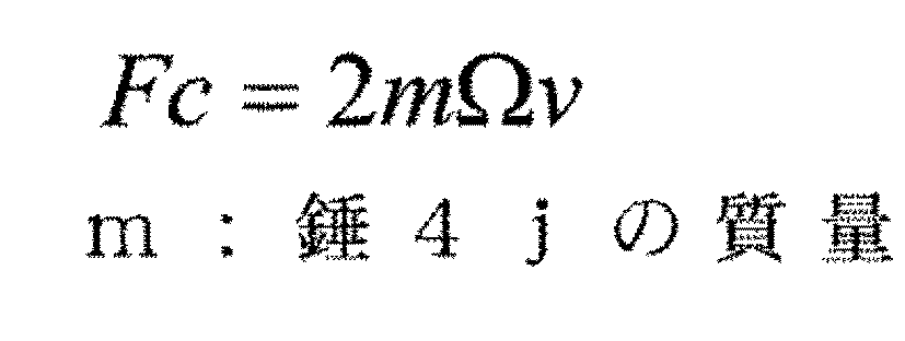
第2の振動体である錘4jは,数9で示すコリオリ力FcによってY軸方向に振動し,検出電極4n,4o間の静電容量が変化する。この静電容量変化を検出することで,Z軸周りの角速度Ωを検出することができる。
なお,第2の振動体である錘4jの変位量の測定方法としては,検出電極4n,4o間の静電容量変化,すなわち,錘4jのY軸方向の変位量が0になるように,電極4n,4o間に印加する電圧をサーボ制御し,その印加電圧より,コリオリ力Fcを求めても良い。
また,互いに対称となるように配置された左側の振動子4q1,右側の振動子4q2を備えるのは,振動子4q1と振動子4q2が互いに逆相に駆動振動させることによって,外部からの加速度をキャンセルしつつ,角速度の検出信号を2個の振動子からの足し合わせとして感度良く検出することと,振動子の振動が外部に漏れにくくすることが可能であるという利点がある。
(実施の形態4)
本発明の構造第4の実施例として複合センサについて述べる。複合センサは,例えば前記加速度センサと前記角速度センサ等の複数のセンサが,一つのパッケージに纏められたものであり,本形態においては,リードフレーム15もしくは,基板22は一つであることを特徴とする。
本発明の構造第4の実施例として複合センサについて述べる。複合センサは,例えば前記加速度センサと前記角速度センサ等の複数のセンサが,一つのパッケージに纏められたものであり,本形態においては,リードフレーム15もしくは,基板22は一つであることを特徴とする。
以下,図15,図16を説明するに当たり,図6乃至図9と同一の構成要素については,その詳細な説明を省略し,異なる点を中心に説明することとする。
チップパッケージの形態は以下の通りである。図7の変形例としてチップパッケージ20aを図15に,図9の変形例としてチップパッケージ21aを図16に示す。
なお,前記複合センサの組み合わせは,一つの加速度センサと一つの角速度センサのみの限りではなく,同じ種類のセンサであっても,異なる種類のセンサであってもどちらでも良く,センサが二個以上で構成されていれば良い。
(実施の形態5)
本発明の構造第5の実施例として前記複合センサの変形例について述べる。本形態においては,複合センサ用の回路基板12bは,複数のセンサの回路基板が一つの基板に作成されていることを特徴とする。
本発明の構造第5の実施例として前記複合センサの変形例について述べる。本形態においては,複合センサ用の回路基板12bは,複数のセンサの回路基板が一つの基板に作成されていることを特徴とする。
以下,図17,図18を説明するに当たり,図6,図7,図8,図9,図15,図16と同一の構成要素については,その詳細な説明を省略し,異なる点を中心に説明することとする。
チップパッケージの形態は以下の通りである。図7の変形例としてチップパッケージ20bを図17,図9の変形例としてチップパッケージ21bを図18に示す。
なお,前記複合センサにおけるセンサチップの組み合わせは,一つの加速度センサチップ11と一つの角速度センサチップ11aの限りではなく,同じ種類のセンサチップの組み合わせであっても,異なる種類のセンサチップの組み合わせであってもどちらでも良く,センサチップが二個以上で構成されていれば良い。
(実施の形態6)
本発明の構造第6の実施例として前記複合センサの変形例について述べる。本形態においては,複合センサのセンサチップ11bは,一つの基板に作成されていることを特徴とする。
本発明の構造第6の実施例として前記複合センサの変形例について述べる。本形態においては,複合センサのセンサチップ11bは,一つの基板に作成されていることを特徴とする。
本構造は,図1乃至図14に示した構造と同様の手法で作成できるが,デバイス基板4で作成する振動体の構造が異なる。以下,図19を説明するに当たり,図1乃至図14と同一の構成要素については,その詳細な説明を省略し,異なる点を中心に説明することとする。
例えば,センサチップ11bの例として,X軸方向の加速度を検出する第一の加速度センシング部40と,前記第一の加速度センシング部に対してXY平面上で直交して配置され,Y軸方向の加速度を検出する第二の加速度センシング部41と,XY平面上に配置されZ軸周りの角速度を検出する角速度センシング部50の組み合わせを挙げ,図4及び図13に示す前記デバイス基板4に形成される振動体構造の変形例を図19に示す。
図19において,前記第一の加速度センシング部40のキャビティ4g1と前記第二の加速度センシング部41のキャビティ4g2は,互いが繋がっていても,独立であっても良い。また,角速度センシング部のキャビティ4g3は,前記キャビティ4g1,4g2のぞれぞれに対して,繋がっていても独立であっても良い。また,前述のように,前記センシング部40,41,50それぞれにおいて,振動体側と外部の回路基板間12bとの電気的接続に使用されるための電極として,それぞれアンカー4d1,4d2,4d3がそれぞれ備わる。このときアンカー4d1,4d2,4d3は前記貫通配線7を介して,キャビティ基板表面のパッド9aに電気的に接続される。そして,パッド9aはワイヤボンディング14を介して回路基板12bに電気的に接続される。
前述のセンサチップ11bは,回路基板12bにワイヤボンディング14を介して接続され,図6,図7もしくは図8,図9と同様に,チップパッケージ21もしくはチップパッケージ22の形態に組み立てられる。
更に,本発明は,加速度センサ,角速度センサ以外にも,キャビティを有するMEMS素子や撮像素子,発光素子等に適用してもよく,前記センサチップの内周部(センシング部)を覆った第一の樹脂と,前記センサチップの外周部を覆った第二の樹脂とを備えた構造とすることで,第一の樹脂でセンサチップを強固に固定するとともに,第二の樹脂でセンシング部を覆うことで,センシング部を保護することができる。
1 キャビティ基板
1a キャビティ部
1b キャビティ上部
1ba キャビティ上部短辺
1bb キャビティ上部長辺
2 領域(センサチップにおいて第一の樹脂に覆われる面)
3 接着材
4 デバイス基板
4a 錘
4b 支持梁
4c アンカー
4d アンカー(貫通配線接続有)
4d1 アンカー(貫通配線接続有,複合センサ・第一の加速度センシング部)
4d2 アンカー(貫通配線接続有,複合センサ・第二の加速度センシング部)
4d3 アンカー(貫通配線接続有,複合センサ・角速度センシング部)
4e 検出電極
4f 固定電極
4g 空洞部
4g1 空洞部(複合センサ・第一の加速度センシング部)
4g2 空洞部(複合センサ・第二の加速度センシング部)
4g3 空洞部(複合センサ・角速度センシング部)
4h 錘(第1の振動体)
4i 支持梁
4j 錘(第2の振動体)
4k 梁(検出用)
4l 駆動電極(錘4h側)
4m 駆動電極(支持基板固定側)
4n 検出電極(錘4j側)
4o 検出電極(支持基板固定側)
4p リンク梁
4q1 振動子
4q2 振動子
5 支持基板
5a キャビティ部
6 絶縁膜
7 貫通配線
8 絶縁膜
9 平面配線
9a パッド
9b 貫通配線上部
10 絶縁膜
10a パッド開口部
11 加速度センサチップ
11a 角速度センサチップ
11b センサチップ(複合センサ)
12 回路基板(加速度センサ用)
12a 回路基板(角速度センサ用)
12b 回路基板(複合センサ用)
13 接着材
14 ワイヤボンディング
15 リードフレーム
16 接着材
17 ワイヤボンディング
18 第一の樹脂
19 第二の樹脂
20 チップパッケージ(リードフレーム型)
20a チップパッケージ変形例(リードフレーム型,複合センサ)
20b チップパッケージ変形例(リードフレーム型,複合センサ)
21 チップパッケージ(基板型)
21a チップパッケージ変形例(基板型,複合センサ)
21b チップパッケージ変形例(基板型,複合センサ)
22 基板
23 パッド
24 配線
25 パッド
26 半田ボール
40 第一の加速度センシング部(複合センサ)
41 第二の加速度センシング部(複合センサ)
50 角速度センシング部(複合センサ)
Claims (15)
- センサチップと,前記センサチップの内周部を覆った第一の樹脂と,前記センサチップの外周部を覆った第二の樹脂とを備えた半導体装置。
- 請求項1記載の半導体装置において,前記センサチップはセンシング部を有し,前記センシング部は前記センサチップの内周部にあり,前記第一の樹脂は前記センシング部に対応する前記センサチップの第一表面を覆い,前記第二の樹脂は前記センシング部に対応しない前記センサチップの第二表面を覆ったことを特徴とする半導体装置。
- 請求項1記載の半導体装置において,前記第一の樹脂と,前記第二の樹脂は,同一の材質であることを特徴とする半導体装置。
- 請求項1記載の半導体装置において,前記第一の樹脂と,前記第二の樹脂は,互いに異なる材質であることを特徴とする半導体。
- 請求項4記載の半導体装置において,前記第一の樹脂は,前記第二の樹脂と比較して,ヤング率が小さいことを特徴とする半導体装置。
- 請求項4記載の半導体装置において,前記第一の樹脂は,光を透過することを特徴とする半導体装置。
- 請求項1乃至6記載の半導体装置の何れかにおいて,前記第一の樹脂は,第一の工程で成形され,前記第二の樹脂は,第二の工程で成形されたことを特徴とする半導体装置。
- 請求項1乃至6記載の半導体装置の何れかにおいて,前記第二の樹脂は,第一の工程で成形され,前記第一の樹脂は,第二の工程で成形されたことを特徴とする半導体装置。
- 請求項6または8記載の半導体装置において,前記各工程において,前記第一の樹脂の成形圧力を,前記第二の樹脂の成形圧力よりも小さくしたことを特徴とする半導体装置。
- 請求項1乃至9記載の半導体装置の何れかにおいて,前記センサチップに空隙を有することを特徴とする半導体装置。
- 請求項10記載の半導体装置において,前記空隙は気密である特徴とする半導体装置。
- 請求項1乃至11記載の半導体装置の何れかにおいて,前記センサチップの材質は半導体もしくはガラスであることを特徴とする半導体装置。
- 請求項1乃至11記載の半導体装置の何れかにおいて,前記センサチップにはワイヤボンディング用のパッドを有し,ワイヤボンディングされていることを特徴とする半導体装置。
- 請求項13記載の半導体装置において,前記パッド及びワイヤボンディングは,前記第二の樹脂で覆われていることを特徴とする半導体センサ装置。
- 請求項13記載の半導体装置において,前記パッド及びワイヤボンディングは,前記第一の樹脂で覆われていることを特徴とする半導体センサ装置。
Priority Applications (1)
| Application Number | Priority Date | Filing Date | Title |
|---|---|---|---|
| JP2017526243A JP6462128B2 (ja) | 2015-07-01 | 2016-06-03 | 半導体装置 |
Applications Claiming Priority (2)
| Application Number | Priority Date | Filing Date | Title |
|---|---|---|---|
| JP2015132313 | 2015-07-01 | ||
| JP2015-132313 | 2015-07-01 |
Publications (1)
| Publication Number | Publication Date |
|---|---|
| WO2017002528A1 true WO2017002528A1 (ja) | 2017-01-05 |
Family
ID=57608513
Family Applications (1)
| Application Number | Title | Priority Date | Filing Date |
|---|---|---|---|
| PCT/JP2016/066528 Ceased WO2017002528A1 (ja) | 2015-07-01 | 2016-06-03 | 半導体装置 |
Country Status (2)
| Country | Link |
|---|---|
| JP (1) | JP6462128B2 (ja) |
| WO (1) | WO2017002528A1 (ja) |
Cited By (1)
| Publication number | Priority date | Publication date | Assignee | Title |
|---|---|---|---|---|
| US20230125187A1 (en) * | 2021-10-27 | 2023-04-27 | Seiko Epson Corporation | Inertial measurement unit |
Citations (4)
| Publication number | Priority date | Publication date | Assignee | Title |
|---|---|---|---|---|
| JPH0883869A (ja) * | 1994-09-09 | 1996-03-26 | Sony Corp | 半導体装置およびその製造方法 |
| JPH09119875A (ja) * | 1995-10-25 | 1997-05-06 | Matsushita Electric Works Ltd | 半導体圧力センサ |
| JP2015007559A (ja) * | 2013-06-25 | 2015-01-15 | セイコーエプソン株式会社 | モジュール、モジュールの製造方法、電子機器及び移動体 |
| JP2015018922A (ja) * | 2013-07-10 | 2015-01-29 | 株式会社デンソー | モールドパッケージの製造方法 |
-
2016
- 2016-06-03 JP JP2017526243A patent/JP6462128B2/ja not_active Expired - Fee Related
- 2016-06-03 WO PCT/JP2016/066528 patent/WO2017002528A1/ja not_active Ceased
Patent Citations (4)
| Publication number | Priority date | Publication date | Assignee | Title |
|---|---|---|---|---|
| JPH0883869A (ja) * | 1994-09-09 | 1996-03-26 | Sony Corp | 半導体装置およびその製造方法 |
| JPH09119875A (ja) * | 1995-10-25 | 1997-05-06 | Matsushita Electric Works Ltd | 半導体圧力センサ |
| JP2015007559A (ja) * | 2013-06-25 | 2015-01-15 | セイコーエプソン株式会社 | モジュール、モジュールの製造方法、電子機器及び移動体 |
| JP2015018922A (ja) * | 2013-07-10 | 2015-01-29 | 株式会社デンソー | モールドパッケージの製造方法 |
Cited By (3)
| Publication number | Priority date | Publication date | Assignee | Title |
|---|---|---|---|---|
| US20230125187A1 (en) * | 2021-10-27 | 2023-04-27 | Seiko Epson Corporation | Inertial measurement unit |
| JP2023064878A (ja) * | 2021-10-27 | 2023-05-12 | セイコーエプソン株式会社 | 慣性計測装置 |
| JP7786125B2 (ja) | 2021-10-27 | 2025-12-16 | セイコーエプソン株式会社 | 慣性計測装置 |
Also Published As
| Publication number | Publication date |
|---|---|
| JP6462128B2 (ja) | 2019-01-30 |
| JPWO2017002528A1 (ja) | 2018-01-25 |
Similar Documents
| Publication | Publication Date | Title |
|---|---|---|
| JP5619824B2 (ja) | 微小電気機械システム | |
| US20100101325A1 (en) | Acceleration sensor | |
| US9632105B2 (en) | Angular velocity sensor for suppressing fluctuation of detection sensitivity | |
| US9321627B2 (en) | Electronic device, electronic module, electronic apparatus, and moving object | |
| US10800651B2 (en) | Low stress integrated device packages | |
| US20140374847A1 (en) | Packaging method for mems devices | |
| US9829505B2 (en) | Electronic device, electronic apparatus, and moving object | |
| JP7786125B2 (ja) | 慣性計測装置 | |
| US20190301866A1 (en) | Physical quantity sensor | |
| JP6343102B2 (ja) | 慣性力センサ | |
| US9790083B2 (en) | Vibrator, manufacturing method of vibrator, electronic device, electronic apparatus, and moving object | |
| JP6512006B2 (ja) | センサ装置 | |
| JP6462128B2 (ja) | 半導体装置 | |
| US20200072607A1 (en) | Sensor device and electronic apparatus | |
| WO2007020701A1 (ja) | 加速度センサ装置 | |
| WO2016121453A1 (ja) | 半導体センサ装置 | |
| EP3614103B1 (en) | Sensor packages | |
| CN113678000B (zh) | 物理量传感器 | |
| JP5776184B2 (ja) | センサ装置 | |
| JP2012194032A (ja) | センサ装置 | |
| JP2014128842A (ja) | Mems素子を有する半導体パッケージ | |
| CN101258408A (zh) | 加速度传感器装置 |
Legal Events
| Date | Code | Title | Description |
|---|---|---|---|
| 121 | Ep: the epo has been informed by wipo that ep was designated in this application |
Ref document number: 16817637 Country of ref document: EP Kind code of ref document: A1 |
|
| ENP | Entry into the national phase |
Ref document number: 2017526243 Country of ref document: JP Kind code of ref document: A |
|
| NENP | Non-entry into the national phase |
Ref country code: DE |
|
| 122 | Ep: pct application non-entry in european phase |
Ref document number: 16817637 Country of ref document: EP Kind code of ref document: A1 |