WO2017002431A1 - システム、アナログデジタル変換器、および、システムの制御方法 - Google Patents
システム、アナログデジタル変換器、および、システムの制御方法 Download PDFInfo
- Publication number
- WO2017002431A1 WO2017002431A1 PCT/JP2016/062244 JP2016062244W WO2017002431A1 WO 2017002431 A1 WO2017002431 A1 WO 2017002431A1 JP 2016062244 W JP2016062244 W JP 2016062244W WO 2017002431 A1 WO2017002431 A1 WO 2017002431A1
- Authority
- WO
- WIPO (PCT)
- Prior art keywords
- signal
- power supply
- analog
- supply voltage
- conversion
- Prior art date
- Legal status (The legal status is an assumption and is not a legal conclusion. Google has not performed a legal analysis and makes no representation as to the accuracy of the status listed.)
- Ceased
Links
Images













Classifications
-
- H—ELECTRICITY
- H03—ELECTRONIC CIRCUITRY
- H03M—CODING; DECODING; CODE CONVERSION IN GENERAL
- H03M1/00—Analogue/digital conversion; Digital/analogue conversion
- H03M1/002—Provisions or arrangements for saving power, e.g. by allowing a sleep mode, using lower supply voltage for downstream stages, using multiple clock domains or by selectively turning on stages when needed
-
- H—ELECTRICITY
- H03—ELECTRONIC CIRCUITRY
- H03M—CODING; DECODING; CODE CONVERSION IN GENERAL
- H03M1/00—Analogue/digital conversion; Digital/analogue conversion
- H03M1/12—Analogue/digital converters
- H03M1/124—Sampling or signal conditioning arrangements specially adapted for A/D converters
- H03M1/1245—Details of sampling arrangements or methods
- H03M1/125—Asynchronous, i.e. free-running operation within each conversion cycle
-
- H—ELECTRICITY
- H03—ELECTRONIC CIRCUITRY
- H03M—CODING; DECODING; CODE CONVERSION IN GENERAL
- H03M1/00—Analogue/digital conversion; Digital/analogue conversion
- H03M1/12—Analogue/digital converters
- H03M1/34—Analogue value compared with reference values
- H03M1/38—Analogue value compared with reference values sequentially only, e.g. successive approximation type
- H03M1/46—Analogue value compared with reference values sequentially only, e.g. successive approximation type with digital/analogue converter for supplying reference values to converter
Definitions
- This technology relates to a system, an analog-digital converter, and a system control method. More specifically, the present invention relates to a system that sequentially compares an analog signal with a reference signal and converts the analog signal into a digital signal, an analog-digital converter, and a system control method.
- an analog-to-digital converter is provided in various electronic devices such as cameras, audio devices, and measuring devices for the purpose of converting an analog signal into a digital signal.
- ADC analog-to-digital converter
- electronic devices such as cameras, audio devices, and measuring devices for the purpose of converting an analog signal into a digital signal.
- successive approximation type ADCs are widely used because power consumption and circuit scale are particularly small.
- the above successive approximation ADC is provided with a comparator, a logic circuit, a DAC (Digital to Analog Converter), and the like (for example, see Non-Patent Document 1).
- a comparator for comparing the reference voltage V DAC from the input voltage V in and the DAC to be converted.
- the logic circuit controls the DAC based on the comparison result to boost or lower the reference voltage V DAC .
- the comparison by the comparator and the adjustment of the reference voltage by the DAC are performed alternately over the same number of times as the resolution of the ADC.
- This technology was created in view of such a situation, and aims to reduce the power consumption of a successive approximation type analog-digital converter.
- the present technology has been made to solve the above-described problems, and a first aspect of the present technology is an analog-digital converter that compares an analog signal with a reference signal and outputs frequency information indicating the number of comparisons. And a power supply voltage generator that generates a power supply voltage based on the number-of-times information and supplies the power supply voltage to the analog-digital converter, and a control method therefor. This brings about the effect that the power supply voltage generated based on the frequency information is supplied to the analog-digital converter.
- the power supply voltage further includes a conversion time measuring unit that measures a conversion time from when the analog signal is sampled until the comparison number indicated by the number information reaches a certain number.
- the generator generates the power supply voltage according to the measured conversion time, the analog-digital converter compares the analog signal and the reference signal to generate the comparison result, Each time a comparison result is generated, a digital signal holding unit that holds the comparison result and outputs a signal indicating the held value as a digital signal, and changes the value of the reference signal based on the digital signal
- a reference signal supply unit that supplies the device and a number information output unit that outputs the number information. This brings about the effect that a power supply voltage corresponding to the measured conversion time is generated.
- the number information output unit outputs the number information over a period from when the analog signal is sampled until a predetermined sampling period elapses, and the conversion time measuring unit. If the sampling period elapses before the number of comparisons reaches the certain number, the conversion time may be obtained from the number of comparisons within the sampling period and the predetermined sampling period. This brings about the effect that the conversion time is obtained from the number of comparisons and the sampling period when the sampling period elapses before the number of comparisons reaches a certain number.
- the power supply voltage generation unit may generate the power supply voltage that is higher as the conversion time is longer. As a result, the longer the conversion time, the higher the power supply voltage is generated.
- the power supply voltage generation unit further includes a power supply voltage calculation unit that calculates a difference between the conversion time and a predetermined target time and calculates a set value of the power supply voltage from the difference.
- the power supply voltage may be generated according to the set value. This brings about the effect that the set value of the power supply voltage is calculated from the difference between the conversion time and the target time.
- the first aspect further includes a conversion time holding unit that holds each of the conversion times measured within a predetermined voltage control period, and the power supply voltage calculation unit is configured to store the conversion time held in the predetermined voltage control period.
- Each statistic may be calculated every time the predetermined voltage control period elapses to obtain a difference between the statistic and the predetermined target time.
- the conversion time holding unit further holds the digital signal in association with each of the conversion times
- the power supply voltage calculation unit is configured to output the digital signal having a specific value.
- a weighting factor smaller than the digital signal other than the specific value may be determined, and the conversion time may be weighted by the weighting factor. This brings about the effect that the power supply voltage is controlled to a voltage corresponding to the conversion time subjected to the weighting calculation.
- the power supply voltage generator may supply a power supply voltage in addition to the reference signal supply unit. This brings about the effect that the power supply voltage is supplied to other than the reference signal supply unit.
- a conversion data processing unit that corrects the conversion data based on the value of the power supply voltage may be further provided. As a result, the conversion data is corrected based on the value of the power supply voltage.
- the power supply voltage generation unit may generate power supply voltages for the plurality of analog-digital converters. This brings about the effect
- the comparator, the digital signal holding unit, the reference signal supply unit, and the frequency information output unit are provided in an analog-digital conversion chip, and the conversion time measurement unit is provided in a control chip. It may be provided. As a result, the power supply voltage of the comparator provided in the analog-digital conversion chip is controlled to a voltage corresponding to the conversion time.
- the analog-digital conversion chip may be provided in an analog-digital converter housing, and the control chip may be provided in a control unit housing. This brings about the effect that the power supply voltage of the comparator provided in the analog-digital converter housing is controlled to a voltage corresponding to the conversion time.
- the first aspect further includes a sensor that generates the analog signal, and a sample and hold circuit that samples and holds the generated analog signal, and the sample and hold circuit includes the analog-to-digital conversion chip.
- the analog-digital conversion chip may be connected to the sensor, and the sensor may be provided in the analog-digital converter housing. As a result, the analog signal generated by the sensor is sampled.
- the digital signal may be further converted to a serial signal and further transmitted to the control unit housing.
- the digital signal is converted into a serial signal and transmitted.
- the digital signal is transmitted to the control unit housing without contact and the control signal indicating the control amount of the power supply voltage is received from the control unit housing without contact.
- a contactless transmission interface that performs processing may be further provided. This brings about the effect that digital signals and control signals are transmitted and received without contact.
- the contactless transmission interface receives the AC signal of power corresponding to the power consumption of the analog-digital converter storage housing from the control unit storage housing in a contactless manner, and compares the comparisons. May be supplied to the vessel. Thereby, the effect
- the contactless transmission interface receives the AC signal in which the control signal is superimposed on a carrier wave in a contactless manner from the control unit housing, and generates a new one based on the carrier wave.
- the digital signal may be superimposed on a simple AC signal and transmitted to the control unit housing. This brings about the effect
- the power supply voltage generator supplies the power supply voltage over a supply period from when the sampling of the analog signal is instructed until the number of comparisons reaches a predetermined number.
- the supply of the power supply voltage is stopped in a period other than the supply period, and the predetermined number of times may not exceed the predetermined number of times.
- the power supply voltage is supplied within the supply period, and the supply of the power supply voltage is stopped during the period outside the supply period.
- the second aspect of the present technology includes a comparator that compares an analog signal and a reference signal to generate a comparison result, and holds the comparison result every time the comparison result is generated.
- a digital signal holding unit that outputs a digital signal
- a reference signal supply unit that changes the value of the reference signal based on the digital signal and supplies the digital signal to the comparator, and the number of comparisons of the analog signal It is an analog-digital converter provided with the frequency information output part which outputs the frequency information shown as. Thereby, the number information indicating the number of comparisons of the analog signals as the number of comparisons is output together with the digital signal.
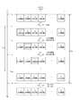
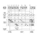
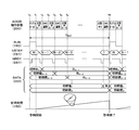
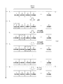
- 4 is a timing chart illustrating an example of the operation of the electronic device when the power supply voltage is low in the first embodiment. It is a figure which shows an example of the conversion data when the power supply voltage in 1st Embodiment is low. It is a flowchart which shows an example of operation
- FIG. 1 is a block diagram illustrating a configuration example of the electronic device 100 according to the first embodiment.
- the electronic device 100 includes a power supply voltage generation unit 110, a power supply voltage calculation unit 120, a storage unit 140, a conversion time measurement unit 150, an ADC control unit 160, a conversion data processing unit 170, and an analog / digital converter 200. These circuits are mounted on the same semiconductor chip, for example.
- the analog-digital converter 200 performs AD (Analog-to-Digital) conversion of the input analog signal AIN into digital conversion data DATA. Each time the start instruction signal RUN is supplied from the ADC control unit 160, the analog-to-digital converter 200 samples the analog signal AIN and AD converts it into converted data DATA. In this AD conversion, the analog-digital converter 200 compares the sampled analog signal AIN with an internally generated reference signal N times (N is an integer), and generates a 1-bit comparison result each time the comparison is performed. The analog-to-digital converter 200 generates N-bit data including the comparison result as converted data DATA, and supplies the converted data to the converted data processing unit 170 via the signal line 209. Here, N is called the resolution of AD conversion, and indicates the number of bits of the digital signal after AD conversion.
- AD Analog-to-Digital
- the analog-digital converter 200 counts the count value every time the analog signal AIN and the reference signal are compared.
- the analog-digital converter 200 generates a comparison counter value NSTEP indicating the count value and a timing signal NRDY for capturing the NSTEP.
- the analog-digital converter 200 supplies the number-of-times information including these to the conversion time measurement unit 150 via the signal line 208.
- the ADC control unit 160 controls the analog / digital converter 200.
- the ADC control unit 160 When the AD conversion is instructed by a user or an external device, the ADC control unit 160 generates a start instruction signal RUN every time a predetermined sampling period Tspl elapses, and the analog-digital converter 200 and the conversion time measuring unit 150 through the signal line 169.
- the conversion time measuring unit 150 measures the time from when the analog signal AIN is sampled until the number of comparisons between the analog signal and the reference signal reaches a predetermined set number S as the conversion time T CNV .
- the conversion time measuring unit 150 takes in the comparison counter value NSTEP in synchronization with the timing signal NRDY. Then, the conversion time measuring unit 150 measures the time until the comparison counter value NSTEP becomes a value corresponding to the set number S as the conversion time T CNV , and the conversion time T CNV is stored via the signal line 159 in the storage unit 140.
- a value less than the resolution (N) of the analog-to-digital converter 200 is set as the set number of times S. For example, when the resolution N is 16 bits, 16 is set in S.
- the unit of the conversion time T CNV is, for example, microseconds ( ⁇ s).
- the analog-digital converter 200 outputs the number information including both the count value (NSTEP) and the timing signal (NRDY), but may be configured to output the number information including only one.
- the conversion time measurement unit 150 counts the number of times the timing signal NRDY is output, obtains the number of comparisons, and measures the time until the number of times reaches the set number S. Good.
- the storage unit 140 holds a certain number of conversion times T CNV .
- the storage unit 140 is an example of a conversion time holding unit described in the claims.
- the power supply voltage calculation unit 120 calculates the voltage control amount ⁇ V from the conversion time T CNV .
- the power source voltage calculation unit 120 reads out the conversion time T CNV measured within the cycle from the storage unit 140 every time a predetermined voltage control cycle elapses, and reads the statistics T STAT (for example, (Moving average value) is calculated.
- the voltage control cycle is a cycle for controlling the power supply voltage of the analog-digital converter 200, and is set to a value equal to or greater than the sampling cycle, for example.
- the power supply voltage calculation unit 120 calculates the voltage control amount ⁇ V by the following equation from the statistic (T STAT ) and the predetermined target time T TAG .
- the target time T TAG is a value equal to or less than the sampling period T spl , and its unit is, for example, microseconds ( ⁇ s).
- ⁇ T T STAT ⁇ T TAG Equation 1
- ⁇ V f ( ⁇ T) Equation 2
- f () is a function having an integral element and a proportional element with respect to ⁇ T. It is also possible to design by adding a differential element, a time delay element, or a nonlinear element according to the target control characteristic.
- F () is a function that returns a value with a negative correlation with respect to the input value ( ⁇ T).
- ⁇ T positive, that is, when the conversion time statistic T STAT is larger than the target time T TAG , ⁇ V is not updated. It is set to a smaller value.
- the integral element output for ⁇ T is 0, if ⁇ T is +0.1 microseconds, ⁇ V is set to ⁇ 0.1 volts, and if ⁇ T is ⁇ 0.1 microseconds, ⁇ V is set to +0. .1 volt is set.
- the voltage control amount ⁇ V is added to the initial voltage V sup0 set in the system to generate the power supply voltage setting value VDD set shown in the following equation.
- VDD set V sup0 + ⁇ V Equation 3
- the power supply voltage calculation unit 120 supplies data indicating the power supply voltage set value VDD set to the power supply voltage generation unit 110 via the signal line 129.
- the power supply voltage calculation unit 120 supplies data indicating the calculated power supply voltage set value VDD set and the initial voltage Vsup0 of the power supply voltage to the conversion data processing unit 170 via the signal line 128.
- the unit of VDD set and V sup0 is, for example, volts (V).
- the power supply voltage generator 110 generates and supplies the power supply voltage VDD of the analog-digital converter 200 according to the power supply voltage setting value VDD set .
- the main power source V ps supplied to the power source voltage generator 110 may be a direct current obtained by rectifying a commercial power source, or a secondary battery or a primary battery.
- the power supply voltage VDD is adjusted to a voltage when the conversion time T CNV becomes a value (T TAG ) equal to or less than the sampling period T spl , that is, when quantization is completed within the sampling period. Therefore, the power supply voltage generation unit 110 can reduce the power supply voltage VDD to a minimum voltage at which quantization is completed within the sampling period Tspl . Thereby, the power consumption of the analog-digital converter 200 can be reduced to a necessary minimum.
- the conversion data processing unit 170 performs predetermined processing such as encoding processing and error correction processing on the conversion data DATA.
- the conversion gain of the analog / digital converter 200 When the power supply voltage VDD of the analog / digital converter 200 varies, generally the conversion gain of the analog / digital converter 200 also varies.
- the conversion gain indicates the ratio of the value of the digital signal (DATA) to the value of the analog signal.
- the conversion gain Ga when the power supply voltage VDD is controlled by ⁇ V changes, for example, according to the following equation.
- Ga Ga 0 ⁇ V sup0 / VDD set Expression 4
- Ga 0 represents a default conversion gain when the power supply voltage VDD is not controlled.
- the conversion gain is inversely proportional to the power supply voltage.
- the conversion data processing unit 170 corrects the conversion data DATA according to the following expression, and calculates corrected conversion data DATA correct .
- the conversion data processing unit 170 outputs the corrected conversion data DATA correct as a processing result.
- DATA correct DATA x VDD set / V sup0 ...
- input data DATA before correction are the value obtained by multiplying the conversion gain Ga in the voltage V in of the analog signal AIN, the following expression holds.
- Equation 6 V in ⁇ Ga 0 ... Equation 7
- power supply voltage dependency of the conversion gain is not limited to the relationship represented by Expression 4, and can take any characteristic, and the compensation characteristic for the characteristic can be appropriately designed instead of Expression 5.
- FIG. 2 is a block diagram illustrating a configuration example of the analog-digital converter 200 according to the first embodiment.
- the analog-digital converter 200 includes a sample hold circuit 210, a comparator 220, a latch circuit 230, a register 250, a DA converter 260, an XOR (exclusive OR) gate 270, and a state machine 280.
- the state machine 280 includes a counter 281 and a sequencer 282.
- the sample hold circuit 210 samples and holds the analog signal AIN when the start instruction signal RUN is supplied.
- the sample hold circuit 210 supplies the held analog signal AIN to the non-inverting input terminal (+) of the comparator 220 as the sample hold signal SHOUT.
- the comparator 220 compares the value (for example, voltage value) between the sample hold signal SHOUT and the reference signal DAOUT from the DA converter 260 in accordance with the comparator control signal CMP.
- the voltage of the sample hold signal SHOUT is referred to as “input voltage”
- the voltage of the reference signal DAOUT is referred to as “reference voltage”.
- the comparator 220 supplies a differential signal indicating the comparison result to the latch circuit 230 and the XOR gate 270 when the comparator control signal CMP is at a high level.
- This differential signal includes a normal phase signal COMPP and a negative phase signal COMPN having different phases.
- the comparator control signal CMP is at the low level, the comparator 220 outputs both the positive phase signal COMPP and the negative phase signal COMPN at the high level.
- the latch circuit 230 holds 1-bit information indicated by the differential signal from the comparator 220.
- the latch circuit 230 includes a set terminal S, a reset terminal R, and an output terminal Q.
- a normal phase signal COMPP is input to the set terminal S
- a negative phase signal COMPN is input to the reset terminal R.
- the latch circuit 230 holds “1” when the set terminal S is at the high level and the reset terminal R is at the low level, and outputs the latch signal SROUT having the value of the hold value from the output terminal Q to the register 250.
- the latch circuit 230 outputs the latch signal SROUT of “0” from the output terminal Q.
- the latch circuit 230 holds the state of the output terminal Q.
- the XOR gate 270 is NANDed. Can be replaced with a gate.
- the comparator 220 when the comparator control signal CMP is at low level, the comparator 220 sets both the normal phase signal COMPP and the negative phase signal COMPN to high level.
- the logic polarity of the input of the latch circuit 230 can be reversed.
- the XOR gate 270 can be replaced with an OR gate.
- the register 250 holds the latch output signal SROUT in accordance with the write control signal rWRITE and the comparison counter value NSTEP.
- the register 250 includes N flip-flops, and holds N-bit conversion data DATA in these flip-flops.
- the register 250 When the start instruction signal RUN is supplied, the register 250 resets the stored conversion data DATA to initial data. For example, the conversion data DATA is reset to initial data in which the most significant bit (MSB: Most Significant Bit) is “1” and all the remaining bits are “0”.
- MSB Most Significant Bit
- the register 250 updates the bit of the digit corresponding to the comparison counter value NSTEP in the conversion data DATA by the latch signal SROUT. For example, the bit of the (N-1-NSTEP) digit from the MSB in the conversion data is updated by the latch output signal SROUT. For example, if the comparison counter value NSTEP is “N ⁇ 1”, the MSB is updated. If the comparison counter value NSTEP is “N ⁇ 2”, the next bit of the MSB is updated.
- the register 250 outputs the updated conversion data DATA to the conversion data processing unit 170 and the DA converter 260 every time the conversion data DATA is updated. Further, the register 250 holds the state of the conversion data DATA in a period other than the rising edge of the write control signal rWRITE.
- the register 250 is an example of a digital signal holding unit described in the claims.
- the DA converter 260 Each time the conversion data DATA is output from the register 250, the DA converter 260 updates the value of the reference signal DAOUT based on the conversion data DATA.
- the DA converter 260 outputs a reference signal DAOUT of 1/2 ⁇ V FS when the conversion data DATA is initial data.
- V FS is the maximum amplitude level of the DA converter 260.
- V DAOUT_k V DAOUT_k ⁇ 1 + (1/2) k + 1 ⁇ V FS Equation 8
- V DAOUT — k ⁇ 1 is the previous reference voltage.
- the DA converter 260 updates the reference voltage to V DAOUT_k according to the following equation.
- the DA converter 260 is an example of a reference signal supply unit described in the claims.
- V DAOUT — k V DAOUT —k ⁇ 1 ⁇ (1/2) k + 1 ⁇ V FS Equation 9
- the MSB is updated from the initial data "1" to "0”
- the DA converter 260 is an example of a reference signal supply unit described in the claims.
- the analog-to-digital converter 200 that sequentially compares an analog signal with a reference signal is generally called a successive approximation ADC.
- the XOR gate 270 generates an exclusive OR signal of the positive phase signal COMPP and the negative phase signal COMPN as the step control signal READY.
- the XOR gate 270 supplies a step control signal READY to the sequencer 282.
- the comparator 220 outputs a differential signal and the XOR gate 270 generates the step control signal READY.
- the comparator 220 outputs a comparison completion signal simultaneously with the comparison result of the single end signal. It is also possible to adopt a configuration in which the comparison completion signal replaces the step control signal READY. In that case, the XOR gate 270 is unnecessary or can be replaced with a buffer or an inverter simply for the purpose of delay alignment and logic polarity alignment.
- the sequencer 282 controls the comparator 220, the register 250, and the counter 281.
- the sequencer 282 supplies a step control signal READY to the counter 281 to control counting, and supplies a signal obtained by inverting the step control signal READY to the register 250 as a write control signal rWRITE.
- the sequencer 282 supplies the start instruction signal RUN to the sample hold circuit 210, the register 250, and the counter 281.
- the sequencer 282 performs comparison control of N pulses over a period from when the start instruction signal RUN is supplied to when N comparisons are completed (for example, when NSTEP is “0”). Generated as signal CMP.
- the comparison control signal CMP is generated by a pulse generator or the like based on the falling edge of the start instruction signal RUN and the rising edge of the step control signal READY.
- the sequencer 282 supplies the comparison control signal CMP to the comparator 220.
- the counter 281 counts the comparison counter value NSTEP in synchronization with the step control signal READY.
- the comparison counter value NSTEP indicates the number of times the sample / hold signal SHOUT is compared in the comparator 220. Further, when the start instruction signal RUN is supplied, the counter 281 resets the comparison counter value NSTEP to an initial value (for example, N).
- the counter 281 decrements the comparison counter value NSTEP in synchronization with the step control signal READY, and supplies the updated comparison counter value NSTEP to the register 250 and the sequencer 282.
- the counter 281 generates a timing signal NRDY in synchronization with the step control signal READY, and supplies the timing signal NRDY to the conversion time measurement unit 150 together with the comparison counter value NSTEP.
- the counter 281 is an example of the number information output unit described in the claims.
- the counter 281 outputs the comparison counter value NSTEP as it is, it may be encoded and output encoded data. In this case, the conversion time measurement unit 150 may decode and process the encoded data. Further, although the down counter that decreases the comparison counter value NSTEP in synchronization with the step control signal READY is used as the counter 281, an up counter that increases the comparison counter value NSTEP may be used instead of the down counter.
- sequencer 282 may further externally output a conversion end signal EOC when N comparisons are completed.
- the comparator 220 operates in synchronization with the timing signal (CMP) generated in the analog-to-digital converter 200 to generate conversion data DATA.
- CMP timing signal
- the analog-to-digital converter 200 that operates in synchronization with the internally generated timing signal is called a self-timing ADC.
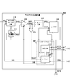
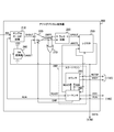
- FIG. 4 is a circuit diagram illustrating a configuration example of the comparator 220 according to the first embodiment.
- the comparator 220 includes transistors 221 to 229.
- Transistors 221 to 224 represent P-type MOS (Metal-Oxide-Semiconductor) transistors, and transistors 225 to 229 represent N-type MOS transistors.
- P-type MOS Metal-Oxide-Semiconductor
- the power supply voltage VDD is applied to the sources of the transistors 221 to 224.
- the gates of transistors 221, 224 and 229 are connected to sequencer 282.
- the gate of the transistor 227 is connected to the sample and hold circuit 210, and the gate of the transistor 228 is connected to the DA converter 260.
- the gates of the transistors 222 and 225 and the drains of the transistors 223 and 224 are connected to the drain of the transistor 226 and the set terminal S of the latch circuit 230.
- the drains of the transistors 221 and 222 and the gates of the transistors 223 and 226 are connected to the drain of the transistor 225 and the reset terminal R of the latch circuit 230.
- the source of the transistor 225 is connected to the drain of the transistor 227, and the source of the transistor 226 is connected to the drain of the transistor 228.
- the sources of the transistors 227 and 228 are connected to the drain of the transistor 229, and the source of the transistor 229 is connected to the ground terminal.
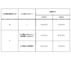
- FIG. 5 is a diagram illustrating an example of the operation of the comparator 220 according to the first embodiment.
- the comparator control signal CMP is “0”
- the comparator 220 outputs a high-level positive phase signal COMPP and a negative phase signal COMPN regardless of the value of the sample hold signal.
- the comparator 220 compares the voltage (input voltage) of the sample hold signal SHOUT with the voltage (reference voltage) of the reference signal DAOUT. If the input voltage is higher than the reference voltage, the comparator 220 outputs a high-level positive-phase signal COMPP and a low-level negative-phase signal COMPN. On the other hand, if the input voltage is equal to or lower than the reference voltage, the comparator 220 outputs a low-level positive-phase signal COMPP and a high-level negative-phase signal COMPN.
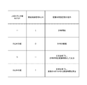
- FIG. 6 is a diagram illustrating an example of the operation of the register 250 according to the first embodiment.
- the N flip-flops constituting the register 250 are initialized to a predetermined value when the start instruction signal RUN is at a high level.
- the register 250 refers to the comparison counter value NSTEP at the rising edge at which the write control signal rWRITE transitions from the low level to the high level, and corresponds to NSTEP in the conversion data DATA.
- the digit bit is updated by the latch output signal SROUT. In other periods, the states of the N flip-flops constituting the register 250 are held.
- FIG. 7 is a diagram illustrating an example of the operation of the conversion time measurement unit 150 according to the first embodiment.
- the conversion time measuring unit 150 starts measuring the conversion time when the start instruction signal RUN falls.
- the conversion time measurement unit 150 counts a timer counter value TIM indicating the measurement time, for example, in synchronization with a clock signal CLK having a constant frequency.
- the conversion time measurement unit 150 When the start instruction signal RUN is at a low level and the comparison counter value NSTEP is a value other than the value indicating the set number of times S (for example, 0), the conversion time measurement unit 150 counts the timer counter value TIM (that is, time count). Continue. When the comparison counter value NSTEP is a value indicating the set number of times S (for example, 0), the conversion time measuring unit 150 ends the time measurement and outputs the measurement time (timer counter value TIM) as the conversion time.
- the conversion time measuring unit 150 ends the time measurement. Then, the conversion time measuring unit 150 calculates the conversion time T CNV from the immediately preceding comparison counter value NSTEP using the following equation and outputs it.
- T CNV ⁇ S / (S-NSTEP) ⁇ ⁇ T spl.
- T spl indicates a sampling period, and the unit is, for example, microseconds ( ⁇ s).
- FIG. 8 is a timing chart illustrating an example of the operation of the analog-digital converter 200 according to the first embodiment.
- the sample hold circuit 210 samples and holds the analog signal AIN, and generates the sample hold signal SHOUT.
- the alternate long and short dash line indicates the locus of the analog signal AIN
- the solid line indicates the locus of the sample hold signal SHOUT.
- the comparison counter value NSTEP is reset to an initial value N, converts the data DATA is reset to the initial data.
- the comparator 220 compares the input voltage (SHOUT) with the reference voltage (DAOUT) and compares the differential signals (COMPP and COMPN). Generate.
- the XOR gate 270 generates a step control signal READY from the differential signal, and the latch circuit 230 holds the comparison result indicated by the differential signal and outputs a latch output signal SROUT. Then, the sequencer 282 generates the write control signal rWRITE by inverting the step control signal READY.
- the counter 281 updates the comparison counter value NSTEP to “N ⁇ 1” in accordance with the step control signal READY.
- the register 250 updates the MSB of the conversion data DATA to BN ⁇ 1 by the latch output signal SROUT according to the write control signal rWRITE.
- DA converter 260 at the timing t 2 when the MSB has been updated by the register 250, a reference signal DAOUT, adjusted based on the MSB.
- the comparator 220 compares the input voltage (SHOUT) and the reference voltage (DAOUT), and generates a differential signal again.
- the XOR gate 270 generates a step control signal READY from the differential signal, and the latch circuit 230 holds the comparison result indicated by the differential signal and outputs a latch output signal SROUT.
- the counter 281 updates the comparison counter value NSTEP to “N ⁇ 2” in accordance with the step control signal READY, and the register 250 sets the next bit of the MSB in the conversion data DATA to B N by the latch output signal SROUT in accordance with the write control signal rWRITE. Update to -2 .
- the DA converter 260 adjusts the reference signal DAOUT based on the B N ⁇ 2 at a timing t 4 when the next bit of the MSB is updated to B N ⁇ 2 in the register 250.
- FIG. 9 is a graph showing an example of a reference voltage adjustment process over time in the first embodiment.
- the vertical axis indicates the voltage of the sample hold signal SHOUT and the reference signal DAOUT
- the horizontal axis indicates time.
- the conversion data DATA is initialized to initial data, and the reference voltage (DAOUT) is initialized to 1 / 2V FS .
- the input voltage (SHOUT) is the reference voltage (1 / 2V FS) below
- MSB of the converted data DATA at the timing t 2 is updated to "0".
- the DA converter 260 decreases the reference signal DAOUT by 1 / 4V FS based on the updated MSB.
- the DA converter 260 increases the reference voltage to 1 / 8V FS based on the updated bit (“1”) to 3 / 8V FS .
- the second bit from the MSB is updated to “0” at timing t 4 . Also, the DA converter 260 decreases the reference voltage by 1 / 16V FS based on the updated bit (“0”).
- the reference voltage is increased or decreased based on the comparison result between the input voltage and the reference voltage, and conversion data DATA including the comparison result is generated.
- FIG. 10 is a timing chart showing details of the operation of the analog-digital converter 200 according to the first embodiment.
- the comparison counter value NSTEP is reset to the initial value N
- the conversion data DATA is reset to the initial data.
- DATA N-1 indicates the MSB of the conversion data DATA.
- comparator 220 When start instruction signal RUN falls at timing t 1 after timing t 0 , comparator 220 generates differential signals (COMPP and COMPN).
- the XOR gate 270 generates the step control signal READY from the differential signal when TC N ⁇ 1 has elapsed from t 1 , and the latch circuit 230 holds the comparison result indicated by the differential signal and generates the latch output signal SROUT Output.
- the sequencer 282 generates the write control signal rWRITE by inverting the step control signal READY.
- TC N ⁇ 1 represents the comparison time of the comparator 220. This comparison time includes a component that increases exponentially when the amplitude of the differential input of the comparator 220 is small.
- the counter 281 updates the comparison counter value NSTEP to “N ⁇ 1” according to the step control signal READY, and the register 250 updates the MSB of the conversion data DATA to B N ⁇ 1 by the latch output signal SROUT according to the write control signal rWRITE. .
- TD1 and TD2 are fixed values generated by the sequencer 282 using a delay line including delay elements.
- FIG. 11 is a timing chart showing an example of the operation of the electronic device 100 when the power supply voltage is high in the first embodiment.
- the sample hold circuit 210 samples and holds the analog signal AIN.
- the start instruction signal when RUN falls at time t 1 the comparator 220 compares the input voltage (SHOUT) and the reference voltage (DAOUT).
- the comparator 220 compares the input voltage (SHOUT) and the reference voltage (DAOUT) again.
- DA converter 260 at the timing t 4 when the next bit of the MSB has been updated by the result of the comparison, the reference signal DAOUT, adjusted based on the bit.
- the comparison by the comparator 220 and the adjustment of the reference signal DAOUT by the DA converter 260 are performed alternately in the same manner. Then, the comparison counter value NSTEP is updated to “0” at the timing t EOC before the sampling period t spl elapses from the timing t 0 , and the AD conversion ends.
- Conversion time measuring unit 150 an analog signal AIN starts measuring the time t 1 which is sampled. Then, the conversion time measuring unit 150 takes in the comparison counter value NSTEP in synchronization with the timing signal NRDY. For example, the comparison counter value NSTEP is captured at the timing when the timing signal NRDY rises to a high level. Then, the timing is finished at the timing t EOC at which the comparison counter value NSTEP “0” is captured. In this way, the conversion time measuring unit 150 takes in the comparison counter value NSTEP at a timing controlled in synchronization with the timing signal NRDY, thereby avoiding the timing at which a glitch occurs in NSTEP in the state machine 280 and comparing counter value NSTEP. Can be imported.
- This conversion time T CNV is composed of the time required for each of N comparisons (TC N-1 etc.) and N TD1 and TD2.
- the former is the comparison time of the comparator 220 as described above with reference to FIG. 10, and the latter is the fixed delay time generated by the sequencer 282.
- the gate-source voltage V GS of the transistor (221 etc.) in the comparator 220 illustrated in FIG. 4 is lower, and the variation in the drain current Id is larger due to the decrease in V GS. Become.
- the variation of Id is larger than that in the non-subthreshold region. Due to the fluctuation of the drain current Id, the operation time of the transistor fluctuates, and the comparison time of the comparator 220 including the transistor fluctuates. That is, as the power supply voltage VDD is lower, the variation in the comparison time of the comparator 220 becomes larger, and the variation in the conversion time T CNV including the comparison time becomes larger.
- the dispersed T CNV becomes longer than the sampling period, AD conversion is not completed within the sampling period, and the error of the conversion data DATA increases rapidly.
- the power supply voltage generator 110 controls the power supply voltage VDD to a higher voltage as the measured conversion time T CNV is longer. As a result, the variation in the conversion time T CNV is reduced, AD conversion is completed within the sampling period, and the error in the conversion data DATA becomes less than the allowable value.
- the power supply voltage VDD of the analog-to-digital converter 200 is set to a sufficiently high value so that an error due to variations in the conversion time T CNV does not exceed an allowable value. There is a need. For this reason, it is difficult to reduce the power consumption of the analog-digital converter 200 to the necessary minimum.
- the electronic device 100 measures the conversion time T CNV, for controlling the power supply voltage VDD to the voltage corresponding to the conversion time T CNV, analog digital minimal value error does not exceed the allowable value
- the power consumption of the converter 200 can be reduced.
- FIG. 12 is a diagram illustrating an example of the conversion data DATA when the power supply voltage is high in the first embodiment.
- start instruction signal RUN When the start instruction signal RUN is input at the timing t 0 , only the leftmost MSB of the conversion data DATA is reset to initial data “1”.
- the comparator 220 compares the input voltage (SHOUT) and the reference voltage (DAOUT) again.
- the next bit of the MSB is updated to, for example, “1” based on the comparison result.
- the DA converter 260 adjusts the reference signal DAOUT based on the updated bit.
- the conversion time measurement unit 150 measures the time from timing t 1 to t EOC and outputs it as the conversion time T CNV , and the power supply voltage generation unit 110 sets the power supply voltage VDD to a voltage corresponding to the conversion time T CNV. To control.
- the conversion time measuring unit 150 finishes counting when the number of comparisons of the analog signal is the resolution N, that is, when the comparison counter value NSTEP is “0” (t EOC ), but is not limited to this configuration. . As illustrated in FIG. 13, the conversion time measurement unit 150 has a predetermined number of analog signal comparisons less than the resolution N (for example, 15), that is, when the comparison counter value NSTEP is “1” (t 30). ) May stop timing.
- FIG. 14 is a timing chart illustrating an example of the operation of the electronic device 100 when the power supply voltage is low according to the first embodiment.
- the lower the power supply voltage VDD the greater the variation in the operation time of the comparator 220 and the DA converter 260.
- This variation in the timing t s of the sampling period T spl has elapsed from the timing t 0, it is assumed that the comparison of N times is not completed.
- Conversion time measuring unit 150 in this case, terminates the counting at the timing t s, the comparison counter value NSTEP immediately before, calculates the conversion time T CNV using Equation 10.
- the conversion time measurement unit 150 can estimate the conversion time T CNV from NSTEP even when the conversion is not completed within the sampling period. it can.
- FIG. 15 is a diagram illustrating an example of the conversion data DATA when the power supply voltage is low in the first embodiment.
- the conversion time T CNV when the power supply voltage is relatively low, variation in the conversion time T CNV becomes large, and AD conversion may not be completed within the sampling period t spl from timing t 0 .
- the least significant bit (LSB: Least Significant Bit) of the conversion data DATA is not updated at the time (t s ) when the sampling period t spl elapses from the timing t 0 and remains the initial value.
- Conversion time measuring unit 150 in this case, terminates the counting at the timing t s, the comparison counter value NSTEP immediately before, calculates the conversion time T CNV using Equation 10.
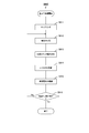
- FIG. 16 is a flowchart illustrating an example of the operation of the electronic device 100 according to the first embodiment. This operation starts when AD conversion is instructed to the electronic device 100.
- the electronic device 100 performs a quantization process for converting the analog signal AIN into the conversion data DATA (step S910). Further, electronic device 100 measures conversion time T CNV (step S901).
- step S902 determines whether or not the sampling period has elapsed.
- step S902 determines whether or not the sampling period has elapsed.
- step S903 the electronic device 100 determines whether or not the voltage control period has elapsed.
- step S904 the electronic device 100 calculates the voltage control amount ⁇ V from the statistical amount of the conversion time T CNV (step S904), and the power supply voltage VDD is calculated based on the voltage control amount ⁇ V. Control is performed (step S905).
- step S903 When the voltage control cycle has not elapsed (step S903: No), or after step S905, the electronic device 100 repeats step S910 and subsequent steps.
- FIG. 17 is a flowchart illustrating an example of the quantization process according to the first embodiment.
- the analog-digital converter 200 samples and holds the analog signal AIN (step S911), and compares the input voltage with the reference voltage (step S912).
- the analog-digital converter 200 decrements the comparison counter value NSTEP (step S913), and updates the register 250 with the comparison result (step S914).
- the analog-to-digital converter 200 increases or decreases the reference voltage based on the comparison result (step S915), and determines whether N comparisons are completed (step S916). Under the condition that the sampling period has not elapsed (FIG. 16: Step S902: No), when N comparisons are not completed (Step S916: No), the analog-digital converter 200 repeats Step S912 and the subsequent steps. .
- step S916 Yes
- step S902 Yes
- the analog-digital converter 200 ends the quantization process.
- the electronic device 100 measures the time until the number of comparisons of analog signals reaches a certain number of times, and sets the power supply voltage to a voltage corresponding to the time.
- the power supply voltage VDD can be reduced to a minimum value. Thereby, the power consumption of the analog-digital converter 200 can be reduced.
- the power supply voltage generation unit 110 controls the power supply voltages of all circuits such as the comparator 220 and the DA converter 260 in the analog-digital converter 200.
- a constant voltage power source that is separately generated can be used for a portion that contributes little to the change in conversion time.
- the electronic device 100 according to the first modification is different from the first embodiment in that only the power supply voltage of some circuits in the analog-digital converter 200 is controlled.
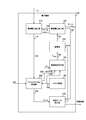
- FIG. 18 is a block diagram illustrating a configuration example of the analog-digital converter 200 according to the first modification of the first embodiment.
- the analog-digital converter 200 according to the first modification is different from the first embodiment in that it further includes a voltage generator 240.
- the voltage generator 240 generates the power supply voltage VDD ′ and supplies it to the DA converter 260 together with the ground voltage.
- the power supply voltage generation unit 110 of the first modified example controls only the power supply voltage VDD to circuits other than the DA converter 260 in the analog-digital converter 200.
- the voltage generator 240 is provided inside the analog-digital converter 200, but may be provided outside. Further, although the voltage generator 240 supplies power only to the DA converter 260, power may be supplied to a portion that contributes little to fluctuations in conversion time.
- the power supply voltage VDD ′ of the DA converter becomes constant regardless of the VDD control, and the conversion gain of the analog-digital converter 200 resulting from the VDD control shown in Expression 4 is increased. Since fluctuation does not occur, conversion gain compensation shown in Equation 5 can be made unnecessary.
- the power supply voltage generation unit 110 continuously supplies the power supply voltage VDD to the analog-digital converter 200.
- the power supply voltage generation unit 110 may supply the power supply voltage VDD intermittently.
- the power supply voltage generation unit of the second modification is different from that of the first embodiment in that the power supply voltage VDD is intermittently supplied.
- FIG. 19 is a block diagram illustrating a configuration example of the electronic device 100 according to the second modification of the first embodiment.
- the electronic device 100 of the second modified example is different from the first embodiment in that a power supply voltage generation unit 111 is provided instead of the power supply voltage generation unit 110.
- analog-digital converter 200 of the second modification further supplies the comparison counter value NSTEP and the timing signal NRDY to the power supply voltage generation unit 111.
- the ADC control unit 160 according to the second modification further supplies the start instruction signal RUN to the power supply voltage generation unit 111.
- the power supply voltage generator 111 turns on the analog-digital converter 200 when the start instruction signal RUN rises. Then, the power supply voltage generator 111 shuts off the power supply of the analog-to-digital converter 200 when it detects that the number of comparisons reaches the maximum value N within the sampling period, that is, when the comparison counter value NSTEP has transitioned to “0”. To do. However, if the comparison counter value NSTEP is not “0” at the timing when the sampling period has elapsed, the power supply is continued.
- FIG. 20 is a timing chart illustrating an example of the operation of the electronic device 100 according to the second modification of the first embodiment.
- the power supply voltage generation unit 111 starts supplying the power supply voltage VDD to the analog-digital converter 200. Then, when it is detected that the comparison counter value NSTEP has transitioned to “0” at the timing t EOC , the power supply voltage generator 111 stops the supply of the power supply voltage VDD.
- the power supply voltage generating section 111 from the timing t 0, the power supply in the period until it detects that NSTEP transitions to "0", the Since power supply is stopped outside the period, power consumption can be reduced.
- the power supply voltage calculation unit 120 controls the power supply voltage VDD based on the average value of the conversion time T CNV .
- the conversion data DATA includes an error that exceeds the allowable range, the conversion time T CNV measured at that time is likely to take an abnormally large value, and if this value is used, the power supply voltage VDD is The value may not be controlled properly.
- the electronic device 100 according to the second embodiment differs from the first embodiment in that the influence of the abnormal value of the conversion time T CNV is reduced.
- FIG. 21 is a block diagram illustrating a configuration example of the electronic device 100 according to the second embodiment.
- the electronic device 100 according to the second embodiment is different from the first embodiment in that a power supply voltage calculation unit 130 is provided instead of the power supply voltage calculation unit 120 and a storage unit 141 is provided instead of the storage unit 140. .
- the conversion data processing unit 170 further supplies the conversion data DATA to the storage unit 141.
- the storage unit 141 stores the conversion time T CNV and the conversion data DATA at that time in association with each other.
- the power supply voltage calculation unit 130 determines a weighting factor based on the conversion data DATA, and calculates a statistic (for example, a weighted average value) by weighting the conversion time T CNV with the weighting factor. Then, the power supply voltage calculation unit 130 calculates a voltage control amount ⁇ V corresponding to the statistic.
- a weighting factor for example, a weighted average value
- FIG. 22 is a block diagram illustrating a configuration example of the power supply voltage calculation unit 130 according to the second embodiment.
- the power supply voltage calculation unit 130 includes a voltage setting unit 131, a weighted average calculation unit 132, and a weighting coefficient determination unit 133.
- the weighting coefficient determination unit 133 determines a weighting coefficient based on the conversion data DATA. Each time the voltage control period elapses, the weight coefficient determination unit 133 reads out the conversion data DATA generated within the period from the storage unit 141. Then, the weighting factor determination unit 133 determines a weighting factor for each conversion data DATA.
- the output of the comparator 220 becomes indefinite when the voltage (SHOUT) of the inverting input terminal (+) and the voltage (DAOUT) of the inverting input terminal ( ⁇ ) substantially coincide.
- This phenomenon is called metastable.
- the weighting factor determination unit 133 determines a small weighting factor for the conversion data DATA that may occur due to a malfunction caused by the metastable.
- the weighted average calculation unit 132 calculates the weighted average of the conversion time T CNV . Each time the voltage control cycle elapses, the weighted average calculation unit 132 reads the conversion time T CNV measured in the cycle from the storage unit 141, and uses the weighting factor determined by the weighting factor determination unit 133 to calculate T CNV weighted average is calculated. The weighted average calculating unit 132 supplies the calculated weighted average TAVG to the voltage setting unit 131.
- Voltage setting unit 131 is configured to set the power supply voltage setting value VDD The set from a weighted average T AVG calculates a voltage control amount [Delta] V. The voltage setting unit 131 calculates the voltage control amount ⁇ V using Equation 1 and Equation 2. The voltage setting unit 131 supplies data indicating the power supply voltage setting value VDD set obtained from the ⁇ V to the power supply voltage generation unit 110, and supplies data indicating the power supply voltage setting value VDDset and the initial voltage V sup0 to the power supply voltage generation unit 110 and The converted data processing unit 170 is supplied.
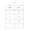
- FIG. 23 is a diagram illustrating an example of data held in the storage unit 141 according to the second embodiment.
- the storage unit 141 holds conversion data DATA in association with the conversion time T CNV .
- the conversion data DATA 1 is generated when the conversion time T CNV1 is measured
- the conversion data DATA 1 is held in association with the conversion time T CNV1 .
- the conversion data DATA 2 is generated when the conversion time T CNV2 is measured
- the conversion data DATA 2 is held in association with the conversion time T CNV2 .
- FIG. 24 is a graph illustrating an example of a relationship between an analog signal and converted data in the second embodiment.
- the vertical axis in the figure shows the value of the conversion data DATA
- a horizontal axis shows an input voltage V in.
- the input voltage V in is a value (for example, V in1 ) different from the reference voltage for comparing the upper bits
- the input voltage V in is converted by the conversion data DATA (for example, DATA 1 ).
- the input voltage V in is likely to occur is metastable if a reference to a voltage substantially coincides to a comparison of the upper bits.
- the analog-digital converter 200 malfunctions and outputs specific values (E1, E2, etc.) depending on the circuit configuration.
- a relatively small weighting coefficient is selected for the conversion time T CNV accompanied with the conversion data E1 and E2 suspected of malfunctioning, and weighted averaging is performed using these weighting coefficients.
- the electronic device 100 reduces the weighting factor by reducing the weighting factor for the conversion data that may have occurred as a result of the malfunction due to the metastable. Since the calculation is performed, it is possible to reduce the influence of errors caused by the metastable.
- the power supply voltage generation unit 110 controls the power supply voltage of one analog-digital converter 200, but can also control the power supply voltages of a plurality of analog-digital converters 200. .
- the power supply voltage generation unit 110 of the third embodiment is different from the first embodiment in that the power supply voltages of the plurality of analog-digital converters 200 are controlled.
- FIG. 25 is a block diagram illustrating a configuration example of the electronic device 100 according to the third embodiment.
- the electronic apparatus 100 according to the third embodiment includes an analog / digital conversion unit 205 including M (M is an integer of 2 or more) analog / digital converters 200 instead of one analog / digital converter 200. However, this is different from the first embodiment.
- the ADC control unit 160 supplies a start instruction signal to the M analog-digital converters 200 to start AD conversion.
- the ADC control unit 160 may cause the M analog-digital converters 200 to start AD conversion at the same time, or may start AD conversion at different timings.
- Each of the M analog-digital converters 200 supplies conversion data to the conversion data processing unit 170 and supplies frequency information (comparison counter value and timing signal) to the conversion time measurement unit 150.
- the conversion time measurement unit 150 calculates M conversion times from the M comparison counter values.
- the conversion time measuring unit 150 causes the storage unit 140 to hold the statistics (average value or maximum value) ST of these M conversion times.
- the power supply voltage generation unit 110 of the third embodiment calculates each statistic (T AVG ) of the statistic ST calculated within the power supply voltage period, and uses the same method as in the first embodiment to generate the voltage. A control amount is calculated.
- the power supply voltage generator 110 according to the third embodiment controls the power supply voltages of the M analog-digital converters 200 at once.
- the power supply voltage generation unit 110 collectively controls the power supply voltages of the M analog-digital converters 200.
- the power supply voltage may be individually controlled for each analog-digital converter 200.
- the conversion time measurement unit 150 does not calculate the statistics of M conversion times, but holds each time in the storage unit 140 for each analog-to-digital converter 200, and the power supply voltage calculation unit 120 The voltage control amount is calculated individually for each digital converter 200.
- the power supply voltage generation unit 110 can collectively control the power supply voltages of the M analog-to-digital converters 200. desirable.
- the power supply voltage generation unit 110 controls the power supply voltages of the plurality of analog-digital converters 200 to values according to the conversion time.
- the power consumption of the converter 200 can be reduced.
- the circuits such as the ADC control unit 160 and the analog-digital converter are provided on the same semiconductor chip. However, these circuits are provided in a distributed manner on a plurality of semiconductor chips. May be.
- the electronic device 100 according to the fourth embodiment is different from the first embodiment in that a circuit is provided in a distributed manner on a plurality of semiconductor chips.
- FIG. 26 is a block diagram illustrating a configuration example of the electronic device 100 according to the fourth embodiment.
- the electronic device 100 includes an AD conversion chip 101 and a control chip 102.
- the AD conversion chip 101 is provided with a power supply voltage generator 110 and an analog / digital converter 200.
- the control chip 102 includes a power supply voltage calculation unit 120, a storage unit 140, a conversion time measurement unit 150, an ADC control unit 160, and a conversion data processing unit 170.
- the AD conversion chip 101 and the control chip 102 are stored in the same housing.
- the power consumption can be reduced in the electronic device 100 including the plurality of semiconductor chips.
- the AD conversion chip 101 and the control chip 102 are stored in the same housing, but they may be stored in different housings.
- the electronic circuit system of the fifth embodiment is different from the fourth embodiment in that each of the AD conversion chip 101 and the control chip 102 is stored in different cases.
- FIG. 27 is a block diagram illustrating a configuration example of an electronic circuit system according to the fifth embodiment.
- This electronic circuit system includes an ADC storage housing 103 and a control unit storage housing 104.
- the ADC storage housing 103 stores the AD conversion chip 101
- the control unit storage housing 104 stores the control chip 102.
- the ADC storage housing 103 and the control unit storage housing 104 are connected by signal lines 127, 168, 206 and 207.
- the power supply voltage calculation unit 120 transmits data indicating the power supply voltage set value VDD set to the power supply voltage generation unit 110 via the signal line 127, and the analog-digital converter 200 transmits the frequency information (NSTEP etc.) via the signal line 206. ) To the conversion time measurement unit 150. Further, the ADC control unit 160 transmits a start instruction signal RUN to the analog-digital converter 200 via the signal line 168, and the analog-digital converter 200 transmits the conversion data DATA to the conversion data processing unit 170 via the signal line 207. Send.
- a power supply circuit for supplying a voltage (V PS ) to the power supply voltage generation unit 110 is omitted in FIG.
- This power supply circuit may be provided in the ADC storage housing 103 or in the control unit storage housing 104.
- each of the AD conversion chip 101 and the control chip 102 is stored in different housings, power consumption is reduced in an electronic circuit system including a plurality of housings. be able to.
- the analog-to-digital converter 200 AD-converts the analog signal generated outside the ADC storage housing 103.
- the analog signal generated inside the ADC storage housing 103 is converted into analog data.
- a / D conversion is also possible.
- the power supply voltage generation unit 110 of the sixth embodiment is different from the fifth embodiment in that the analog-to-digital converter 200 performs AD conversion on an analog signal generated inside the ADC housing 103.
- FIG. 28 is a block diagram illustrating a configuration example of an electronic circuit system according to the sixth embodiment.
- the ADC storage housing 103 according to the sixth embodiment includes a sensor array 305 and an AD conversion chip 101.
- the sensor array 305 includes M sensors 300.
- the AD conversion chip 101 includes M analog-digital converters 200. These M analog-digital converters 200 are connected to the sensor 300 on a one-to-one basis.
- the electronic circuit system includes M sets of the sensor 300 and the analog-digital converter 200, but may have a configuration including only one set.
- the sensor 300 measures a predetermined physical quantity such as temperature, light quantity, or volume.
- the sensor 300 transmits an analog signal indicating a measured value to the corresponding analog-to-digital converter 200.
- ADC storage housing 103 and the control unit storage housing 104 are connected by signal lines 117, 118, 168, 206 and 207.
- FIG. 29 is a block diagram illustrating a configuration example of the control unit storage housing 104 according to the sixth embodiment.
- the control unit housing 104 is provided with a control chip 102.
- the control chip 102 according to the sixth embodiment is different from the first embodiment in that it further includes a power supply voltage generation unit 110.
- the power supply voltage generator 110 supplies a power supply voltage to the sensor array 305 via the signal line 117 and supplies a power supply voltage to the AD conversion chip 101 via the signal line 118.
- the power supply voltage generation unit 110 is provided in the control unit housing 104, but may be provided in the ADC housing 103 as in the fifth embodiment.
- the voltage control unit 110 controls the power supply voltage of the ADC storage housing 103 in which the sensor 300 is incorporated, the power consumption in the housing in which the sensor 300 is incorporated. Can be reduced.
- signals such as comparison counter values and conversion data are transmitted in parallel between the ADC storage housing 103 and the control unit storage housing 104.
- the number of signal lines may increase as the amount of data of these signals increases.
- the electronic circuit system according to the seventh embodiment is different from the sixth embodiment in that the number of signal lines between the housings is reduced.
- FIG. 30 is a block diagram illustrating a configuration example of an electronic circuit system according to the seventh embodiment.
- the electronic circuit system according to the seventh embodiment is different from the first embodiment in that the transmission interface 310 is further stored in the ADC storage housing 103.
- the transmission interface 310 has a function of converting a parallel signal into a serial signal and a function of converting a serial signal into a parallel signal.
- the transmission interface 310 receives parallel signals such as conversion data DATA and comparison counter value NSTEP from the AD conversion chip 101 and converts the parallel signals into serial signals. Then, the transmission interface 310 transmits the serial signal to the control unit storage housing 104 via the signal line 319. Further, the transmission interface 310 receives the start instruction signal RUN from the control unit storage housing 104 via the signal line 319 and supplies it to the AD conversion chip 101.
- ADC storage housing 103 and the control unit storage housing 104 are connected by signal lines 116, 117, 118 and 319.
- FIG. 31 is a block diagram illustrating a configuration example of the control unit storage housing 104 according to the seventh embodiment.
- the control unit storage housing 104 according to the seventh embodiment includes a transmission interface 180 and a control chip 102.
- the transmission interface 180 has a function of converting a parallel signal into a serial signal and a function of converting a serial signal into a parallel signal.
- the transmission interface 180 receives a serial signal from the ADC storage housing 103 via the signal line 319 and converts the serial signal into a parallel signal such as conversion data DATA or a comparison counter value NSTEP.
- the transmission interface 180 supplies conversion data DATA and the like to the control chip 102.
- the transmission interface 180 receives the start instruction signal RUN from the control chip 102 and transmits the signal to the ADC storage housing 103 via the signal line 319.
- the power supply voltage generation unit 110 supplies a power supply voltage to the transmission interface 310, the sensor array 305, and the AD conversion chip 101 via the signal lines 116, 117, and 118.
- the power supply voltage generation unit 110 is provided in the control unit housing 104, but may be provided in the ADC housing 103 as in the fifth embodiment.
- the transmission interface 180 may convert a parallel control signal indicating the voltage control amount into a serial signal and transmit the serial signal to the ADC storage housing 103.
- the transmission interface 310 converts the parallel signal into a serial signal and transmits the serial signal to the control unit housing 104, the parallel signal is transmitted and received between the housings.
- the number of signal lines can be reduced as compared with the case.
- the ADC storage case 103 and the control unit storage case 104 transmit and receive power and data via wires, but they may be transmitted without contact.
- the electronic circuit system of the eighth embodiment is different from the seventh embodiment in that power and data are transmitted and received in a non-contact manner between the casings.
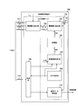
- FIG. 32 is a block diagram illustrating a configuration example of an electronic circuit system according to the eighth embodiment.
- the ADC storage housing 103 of the eighth embodiment is different from the seventh embodiment in that a contactless transmission interface 320 is provided instead of the transmission interface 310.
- the AD conversion chip 101 according to the eighth embodiment includes a power supply voltage generation unit 110 and an analog / digital conversion unit 205.
- the analog-digital conversion unit 205 is provided with M analog-digital converters 200.
- the contactless transmission interface 320 transmits power and data in a contactless manner.
- the non-contact transmission interface 320 receives an AC signal in which a control signal and a start instruction signal RUN are superimposed on a carrier wave from the control unit housing 104 in a non-contact manner. Then, the non-contact transmission interface 320 extracts the control signal and the start instruction signal RUN from the AC signal by demodulation, and supplies the control signal and the start instruction signal RUN to the AD conversion chip 101 together with the voltage V sup0 corresponding to the received power.
- the non-contact transmission interface 320 extracts a carrier wave from the received AC signal and generates an AC signal based on the carrier wave. Then, the non-contact transmission interface 320 superimposes the comparison counter value NSTEP, the timing signal NRDY, and the conversion data DATA from the AD conversion chip 101 on the generated AC signal and transmits them to the control unit housing 104 in a non-contact manner.
- Various methods such as an electromagnetic induction method, an electromagnetic resonance method, and an electric field coupling method can be used as a method for transmitting power and data in a non-contact manner in the non-contact transmission interface 320.
- various standards such as Qi (registered trademark) standard, PMA (Power Matters Alliance) standard, A4WP standard, NFC (Near Field Communication) standard, and the like can be used.
- FIG. 33 is a block diagram illustrating a configuration example of the control unit storage housing 104 according to the eighth embodiment.
- the control unit storage housing 104 of the eighth embodiment is different from the seventh embodiment in that the power supply voltage generation unit 110 is not provided and a contactless transmission interface 190 is provided instead of the transmission interface 180.
- the contactless transmission interface 190 transmits power and data in a contactless manner.
- the non-contact transmission interface 190 transmits an AC signal superimposed with data (VDD set ) to the ADC storage housing 103 in a non-contact manner, and receives an AC signal from the ADC storage housing 103 in a non-contact manner for comparison.
- the counter value NSTEP etc. is taken out.
- the contactless transmission interface 320 since the contactless transmission interface 320 receives power and data from the control unit storage housing 104 in a contactless manner, a signal line is wired between the housings. The power and data can be transmitted without going through the signal line.
- the processing procedure described in the above embodiment may be regarded as a method having a series of these procedures, and a program for causing a computer to execute these series of procedures or a recording medium storing the program. You may catch it.
- a recording medium for example, a CD (Compact Disc), an MD (MiniDisc), a DVD (Digital Versatile Disc), a memory card, a Blu-ray disc (Blu-ray (registered trademark) Disc), or the like can be used.
- this technique can also take the following structures.
- an analog-digital converter that compares the analog signal with the reference signal and outputs the number-of-times information indicating the number of comparisons;
- a system comprising: a power supply voltage generation unit that generates a power supply voltage based on the frequency information and supplies the power supply voltage to the analog-digital converter.
- the power supply voltage generator generates the power supply voltage according to the measured conversion time
- the analog-digital converter is A comparator that compares the analog signal with the reference signal to generate the comparison result;
- a digital signal holding unit that holds the comparison result and outputs a signal indicating the hold value as a digital signal each time the comparison result is generated;
- a reference signal supply unit that changes the value of the reference signal based on the digital signal and supplies the reference signal to the comparator;
- the system according to (1) further including a frequency information output unit that outputs the frequency information.
- the number information output unit outputs the number information over a period from when the analog signal is sampled until a predetermined sampling period elapses,
- the conversion time measurement unit obtains the conversion time from the comparison number in the sampling period and the predetermined sampling period when the sampling period elapses before the comparison number reaches the predetermined number.
- the system described The system described.
- the power supply voltage generation unit generates the power supply voltage that is higher as the conversion time is longer.
- It further includes a power supply voltage calculation unit that calculates a difference between the conversion time and a predetermined target time and calculates a set value of the power supply voltage from the difference.
- (6) further comprising a conversion time holding unit for holding each of the conversion times measured within a predetermined voltage control period;
- the power supply voltage calculation unit calculates each statistic of the held conversion time every time the predetermined voltage control period elapses, and obtains a difference between the statistic and the predetermined target time (5 ) System described.
- the conversion time holding unit further holds the digital signal in association with each of the conversion times,
- the power supply voltage calculation unit determines a weighting coefficient smaller than the digital signal other than the specific value for the digital signal having a specific value, and performs a weighting operation of the conversion time using the weighting coefficient.
- the analog-digital conversion chip is provided in an analog-digital converter housing, The system according to (11), wherein the control chip is provided in a control unit housing. (13) a sensor that generates the analog signal; A sample hold circuit for sampling and holding the generated analog signal; and The sample hold circuit is provided in the analog-digital conversion chip, The analog-digital conversion chip is connected to the sensor, The system according to (12), wherein the sensor is provided in the analog-digital converter housing. (14) The system according to (12) or (13), further including a transmission interface that converts the digital signal into a serial signal and transmits the serial signal to the control unit housing.
- Non-contact performing a process of transmitting the digital signal to the control unit housing without contact and a process of receiving a control signal indicating the control amount of the power supply voltage from the control unit housing without contact.
- the contactless transmission interface receives an AC signal of power corresponding to the power consumption of the analog-digital converter storage housing from the control unit storage housing in a contactless manner and supplies the AC signal to the comparator ( 15) The system described.
- the contactless transmission interface receives the AC signal in which the control signal is superimposed on a carrier wave in a contactless manner from the control unit housing, and adds the digital signal to the new AC signal generated based on the carrier wave.
- the power supply voltage generation unit supplies the power supply voltage over a supply period from when the sampling of the analog signal is instructed until the number of comparisons reaches a predetermined number, and in a period other than the supply period Stop supplying the power supply voltage;
- a comparator that compares the analog signal with the reference signal to generate a comparison result
- a digital signal holding unit that holds the comparison result and outputs a digital signal composed of the comparison result each time the comparison result is generated
- a reference signal supply unit that changes the value of the reference signal based on the digital signal and supplies the reference signal to the comparator
- An analog-digital converter comprising a number information output unit that outputs number information indicating the number of comparisons of the analog signals as a comparison number.
- a system control method comprising: a power supply voltage generation procedure for generating a power supply voltage based on the frequency information and supplying the power supply voltage to the analog-digital converter.
Landscapes
- Engineering & Computer Science (AREA)
- Theoretical Computer Science (AREA)
- Analogue/Digital Conversion (AREA)
Abstract
Description
1.第1の実施の形態(変換時間に応じた電圧に制御する例)
2.第2の実施の形態(重み付け演算した変換時間に応じた電圧に制御する例)
3.第3の実施の形態(複数のADCの電源電圧を変換時間に応じて制御する例)
4.第4の実施の形態(複数のチップからなる電子機器において変換時間に応じた電圧に制御する例)
5.第5の実施の形態(複数の筐体からなる電子回路システムにおいて変換時間に応じた電圧に制御する例)
6.第6の実施の形態(センサを内蔵した筐体の電源電圧を変換時間に応じた電圧に制御する例)
7.第7の実施の形態(シリアル信号を送受信し、変換時間に応じた電圧に制御する例)
8.第8の実施の形態(電力およびデータを非接触で伝送し、変換時間に応じた電圧に制御する例)
[電子機器の構成例]
図1は、第1の実施の形態における電子機器100の一構成例を示すブロック図である。この電子機器100は、電源電圧発生部110、電源電圧算出部120、記憶部140、変換時間測定部150、ADC制御部160、変換データ処理部170およびアナログデジタル変換器200を備える。これらの回路は、例えば、同一の半導体チップに搭載される。
ΔT=TSTAT―TTAG ・・・式1
ΔV=f(ΔT) ・・・式2
上式において、f()はΔTに対する積分要素と比例要素を持つ関数である。なお目標とする制御特性に応じて微分要素やむだ時間要素や非線形要素を加えて設計することも可能である。また、f()は入力値(ΔT)に対し負の相関で値を返す関数であり、ΔTが正、即ち変換時間の統計量TSTATが目標時間TTAGより大きい場合にはΔVが更新前より小さい値になるように設定される。一例として、ΔTに対する積分要素出力が0の場合、ΔTが+0.1マイクロ秒であれば、ΔVに-0.1ボルトが設定され、ΔTが-0.1マイクロ秒であれば、ΔVに+0.1ボルトが設定される。電圧制御量ΔVはシステムに設定されている初期電圧Vsup0に加算され、次の式に示す電源電圧設定値VDDsetを生成する。
VDDset=Vsup0+ΔV ・・・式3
電源電圧算出部120は電源電圧設定値VDDsetを示すデータを電源電圧発生部110に信号線129を介して供給する。
Ga=Ga0×Vsup0/VDDset ・・・式4
上式において、Ga0は、電源電圧VDDを制御しない場合のデフォルトの変換ゲインを示し、この例では変換ゲインは電源電圧に反比例する。
DATAcorrect=DATA×VDDset/Vsup0 ・・・式5
DATA=Vin×Ga
=Vin×Ga0×Vsup0/VDDset ・・・式6
DATAcorrect=Vin×Ga0 ・・・式7
上式に示すように、補正によって、電源電圧VDDの変動に依存しない変換データDATAcorrectが得られる。これにより、動的に電源電圧を制御した電子機器100において、安定な変換ゲインを得ることができる。なお、変換ゲインの電源電圧依存性は式4に表される関係に限定せず任意の特性をとることができ、それに対する補償特性も式5の代わりに適切に設計可能である。
図2は、第1の実施の形態におけるアナログデジタル変換器200の一構成例を示すブロック図である。このアナログデジタル変換器200は、サンプルホールド回路210、比較器220、ラッチ回路230、レジスタ250、DA変換器260、XOR(排他的論理和)ゲート270、ステートマシン280を備える。また、ステートマシン280は、カウンタ281およびシーケンサ282を備える。
VDAOUT_k=VDAOUT_k-1+(1/2)k+1×VFS ・・・式8
上式において、VDAOUT_k-1は、前回の参照電圧である。
VDAOUT_k=VDAOUT_k-1-(1/2)k+1×VFS ・・・式9
例えば、MSBが初期データ「1」から「0」に更新されると、1/2×VFSを1/4×VFS下降させた1/4×VFSが次の参照電圧VDAOUT_1として供給される。なお、DA変換器260は、特許請求の範囲に記載の参照信号供給部の一例である。
図4は、第1の実施の形態における比較器220の一構成例を示す回路図である。この比較器220は、トランジスタ221乃至229を備える。トランジスタ221乃至224はP型のMOS(Metal-Oxide-Semiconductor)トランジスタ、トランジスタ225乃至229はN型のMOSトランジスタを表す。
図5は、第1の実施の形態における比較器220の動作の一例を示す図である。この比較器220は、比較器制御信号CMPが「0」である場合に、サンプルホールド信号の値に関わらずに、ハイレベルの正相信号COMPPおよび逆相信号COMPNを出力する。
図7は、第1の実施の形態における変換時間測定部150の動作の一例を示す図である。この変換時間測定部150は、開始指示信号RUNが立ち下がったときに変換時間の計時を開始する。変換時間の計測において、変換時間測定部150は、例えば、一定周波数のクロック信号CLKに同期して、計測時間を示すタイマカウンタ値TIMを計数する。
TCNV={S/(S-NSTEP)}×Tspl ・・・式10
上式においてTsplは、サンプリング周期を示し、単位は、例えば、マイクロ秒(μs)である。
図8は、第1の実施の形態におけるアナログデジタル変換器200の動作の一例を示すタイミングチャートである。タイミングt0において開始指示信号RUNが入力されると、サンプルホールド回路210は、そのアナログ信号AINをサンプリングして保持し、サンプルホールド信号SHOUTを生成する。同図において、一点鎖線はアナログ信号AINの軌跡を示し、実線はサンプルホールド信号SHOUTの軌跡を示す。
上述の第1の実施の形態では、電源電圧発生部110は、アナログデジタル変換器200内の比較器220やDA変換器260などの全ての回路の電源電圧を制御していた。この内、変換時間の変動に寄与が小さい部分には別途発生する定電圧電源を利用することも可能である。この第1の変形例の電子機器100は、アナログデジタル変換器200内の一部の回路の電源電圧のみを制御する点において第1の実施の形態と異なる。
上述の第1の実施の形態では、電源電圧発生部110は、アナログデジタル変換器200に対し、連続して電源電圧VDDを供給していた。しかし、消費電力を低減する観点から、電源電圧発生部110は、間欠的に電源電圧VDDを供給してもよい。この第2の変形例の電源電圧発生部は、間欠的に電源電圧VDDを供給する点において第1の実施の形態と異なる。
上述の第1の実施の形態では、電源電圧算出部120は、変換時間TCNVの平均値に基づいて電源電圧VDDを制御していた。しかし、変換データDATAが許容範囲以上の誤差を含んでいる場合には、そのときに測定される変換時間TCNVは異常に大きな値をとる可能性が高く、その値を用いると電源電圧VDDが適切な値に制御されないおそれがある。第2の実施の形態の電子機器100は、変換時間TCNVの異常値の影響を軽減した点において第1の実施の形態と異なる。
上述の第1の実施の形態では、電源電圧発生部110は、1つのアナログデジタル変換器200の電源電圧を制御していたが、複数のアナログデジタル変換器200の電源電圧を制御することもできる。この第3の実施の形態の電源電圧発生部110は、複数のアナログデジタル変換器200の電源電圧を制御する点において第1の実施の形態と異なる。
上述の第1の実施の形態では、電子機器100において、ADC制御部160やアナログデジタル変換器などの各回路を同一の半導体チップに設けていたが、これらを複数の半導体チップに分散して設けてもよい。この第4の実施の形態の電子機器100は、複数の半導体チップに分散して回路が設けられている点において第1の実施の形態と異なる。
上述の第4の実施の形態では、AD変換チップ101および制御チップ102を同一の筐体に格納していたが、これらを異なる筐体に格納してもよい。この第5の実施の形態の電子回路システムは、AD変換チップ101および制御チップ102のそれぞれを異なる筐体に格納した点において第4の実施の形態と異なる。
上述の第5の実施の形態では、ADC格納筐体103の外部で生成されたアナログ信号をアナログデジタル変換器200がAD変換していたが、ADC格納筐体103の内部で生成したアナログ信号をAD変換することもできる。この第6の実施の形態の電源電圧発生部110は、アナログデジタル変換器200が、ADC格納筐体103の内部で生成したアナログ信号をAD変換する点において第5の実施の形態と異なる。
上述の第6の実施の形態では、ADC格納筐体103と制御部格納筐体104との間で比較カウンタ値および変換データなどの信号をパラレル形式で伝送していた。しかし、これらの信号のデータ量が多くなるほど信号線の本数が増加するおそれがある。この第7の実施の形態の電子回路システムは、筐体間の信号線の本数を削減した点において第6の実施の形態と異なる。
上述の第7の実施の形態では、ADC格納筐体103および制御部格納筐体104は、電力およびデータを有線で送受信していたが、これらを非接触で伝送してもよい。第8の実施の形態の電子回路システムは、筐体間で電力およびデータを非接触で送受信する点において第7の実施の形態と異なる。
(1)アナログ信号と参照信号とを比較して当該比較回数を示す回数情報を出力するアナログデジタル変換器と、
前記回数情報に基づいて電源電圧を生成して前記アナログデジタル変換器に供給する電源電圧発生部と
を具備するシステム。
(2)前記アナログ信号がサンプリングされたときから前記回数情報の示す前記比較回数が一定回数に達するまでの変換時間を測定する変換時間測定部をさらに具備し、
前記電源電圧発生部は、前記測定された変換時間に応じた前記電源電圧を生成し、
前記アナログデジタル変換器は、
前記アナログ信号と前記参照信号とを比較して前記比較結果を生成する比較器と、
前記比較結果が生成されるたびに当該比較結果を保持して当該保持値を示す信号をデジタル信号として出力するデジタル信号保持部と、
前記デジタル信号に基づいて前記参照信号の値を変更して前記比較器に供給する参照信号供給部と、
前記回数情報を出力する回数情報出力部と
を備える
前記(1)記載のシステム。
(3)前記回数情報出力部は、前記アナログ信号がサンプリングされたときから所定のサンプリング周期が経過するまでの期間に亘って前記回数情報を出力し、
前記変換時間測定部は、前記比較回数が前記一定回数に達する前に前記サンプリング周期が経過した場合には前記サンプリング周期内の前記比較回数と前記所定のサンプリング周期とから前記変換時間を求める
前記(2)記載のシステム。
(4)前記電源電圧発生部は、前記変換時間が長いほど高い前記電源電圧を生成する
前記(2)または(3)記載のシステム。
(5)前記変換時間と所定の目標時間との差分を求めて当該差分から前記電源電圧の設定値を算出する電源電圧算出部をさらに具備し、
前記電源電圧発生部は、前記設定値に従って前記電源電圧を生成する
前記(2)から(4)のいずれかに記載のシステム。
(6)所定の電圧制御周期内において測定された前記変換時間のそれぞれを保持する変換時間保持部をさらに具備し、
前記電源電圧算出部は、前記保持された変換時間のそれぞれの統計量を前記所定の電圧制御周期が経過するたびに算出して当該統計量と前記所定の目標時間との差分を求める
前記(5)記載のシステム。
(7)前記変換時間保持部は、前記変換時間のそれぞれに対応付けて前記デジタル信号をさらに保持し、
前記電源電圧算出部は、特定の値の前記デジタル信号に対して前記特定の値以外のデジタル信号より小さい重み係数を決定して当該重み係数により前記変換時間の重み付け演算を行う
前記(6)記載のシステム。
(8)前記電源電圧発生部は、前記参照信号供給部以外に電源電圧を供給する
前記(2)から(7)のいずれかに記載のシステム。
(9)前記電源電圧の値に基づいて前記変換データを補正する変換データ処理部をさらに具備する前記(8)記載のシステム。
(10)前記電源電圧発生部は、複数の前記アナログデジタル変換器のそれぞれの電源電圧を生成する
前記(2)から(9)のいずれかに記載のシステム。
(11)前記アナログデジタル変換器は、アナログデジタル変換チップに設けられ、
前記変換時間測定部は、制御チップに設けられる
前記(2)から(10)のいずれかに記載のシステム。
(12)前記アナログデジタル変換チップは、アナログデジタル変換器格納筐体に設けられ、
前記制御チップは、制御部格納筐体に設けられる
前記(11)記載のシステム。
(13)前記アナログ信号を生成するセンサと、
前記生成されたアナログ信号をサンプリングして保持するサンプルホールド回路と
をさらに具備し、
前記サンプルホールド回路は、前記アナログデジタル変換チップに設けられ、
前記アナログデジタル変換チップは、前記センサに接続され、
前記センサは、前記アナログデジタル変換器格納筐体に設けられる
前記(12)記載のシステム。
(14)前記デジタル信号をシリアル信号に変換して前記制御部格納筐体に送信する伝送インターフェースをさらに具備する
前記(12)または(13)に記載のシステム。
(15)前記デジタル信号を前記制御部格納筐体に非接触で送信する処理と前記電源電圧の制御量を示す制御信号を前記制御部格納筐体から非接触で受信する処理とを行う非接触伝送インターフェースをさらに具備する
前記(12)または(13)に記載のシステム。
(16)前記非接触伝送インターフェースは、前記制御部格納筐体から前記アナログデジタル変換器格納筐体の消費電力に応じた電力の交流信号を非接触で受電して前記比較器に供給する
前記(15)記載のシステム。
(17)前記非接触伝送インターフェースは、前記制御信号が搬送波に重畳された前記交流信号を非接触で前記制御部格納筐体から受信し、前記搬送波に基づいて生成した新たな交流信号に前記デジタル信号を重畳して前記制御部格納筐体に送信する
前記(16)記載のシステム。
(18)前記電源電圧発生部は、前記アナログ信号のサンプリングが指示されたときから前記比較回数が所定回数に達するまでの供給期間に亘って前記電源電圧を供給し、前記供給期間以外の期間において前記電源電圧の供給を停止し、
前記一定回数は前記所定回数を超えない
前記(2)から(17)のいずれかに記載のシステム。
(19)アナログ信号と参照信号とを比較して比較結果を生成する比較器と、
前記比較結果が生成されるたびに当該比較結果を保持して前記比較結果からなるデジタル信号を出力するデジタル信号保持部と、
前記デジタル信号に基づいて前記参照信号の値を変更して前記比較器に供給する参照信号供給部と、
前記アナログ信号が比較された回数を比較回数として示す回数情報を出力する回数情報出力部と
を具備するアナログデジタル変換器。
(20)アナログ信号と参照信号とを比較して当該比較回数を示す回数情報を出力するアナログデジタル変換手順と、
前記回数情報に基づいて電源電圧を生成して前記アナログデジタル変換器に供給する電源電圧発生手順と
を具備するシステムの制御方法。
101 AD変換チップ
102 制御チップ
103 ADC格納筐体
104 制御部格納筐体
110、111 電源電圧発生部
120、130 電源電圧算出部
131 電圧設定部
132 重み付け平均演算部
133 重み係数決定部
140、141 記憶部
150 変換時間測定部
160 ADC制御部
170 変換データ処理部
180、310 伝送インターフェース
190、320 非接触伝送インターフェース
200 アナログデジタル変換器
205 アナログデジタル変換部
210 サンプルホールド回路
220 比較器
221~229 トランジスタ
230 ラッチ回路
240 電圧発生部
250 レジスタ
260 DA変換器
270 XOR(排他的論理和)ゲート
280 ステートマシン
281 カウンタ
282 シーケンサ
283 NOT(否定)ゲート
284 変換終了信号生成部
300 センサ
305 センサアレイ
Claims (20)
- アナログ信号と参照信号とを比較して当該比較回数を示す回数情報を出力するアナログデジタル変換器と、
前記回数情報に基づいて電源電圧を生成して前記アナログデジタル変換器に供給する電源電圧発生部と
を具備するシステム。 - 前記アナログ信号がサンプリングされたときから前記回数情報の示す前記比較回数が一定回数に達するまでの変換時間を測定する変換時間測定部をさらに具備し、
前記電源電圧発生部は、前記測定された変換時間に応じた前記電源電圧を生成し、
前記アナログデジタル変換器は、
前記アナログ信号と前記参照信号とを比較して前記比較結果を生成する比較器と、
前記比較結果が生成されるたびに当該比較結果を保持して当該保持値を示す信号をデジタル信号として出力するデジタル信号保持部と、
前記デジタル信号に基づいて前記参照信号の値を変更して前記比較器に供給する参照信号供給部と、
前記回数情報を出力する回数情報出力部と
を備える
請求項1記載のシステム。 - 前記回数情報出力部は、前記アナログ信号がサンプリングされたときから所定のサンプリング周期が経過するまでの期間に亘って前記回数情報を出力し、
前記変換時間測定部は、前記比較回数が前記一定回数に達する前に前記サンプリング周期が経過した場合には前記サンプリング周期内の前記比較回数と前記所定のサンプリング周期とから前記変換時間を求める
請求項2記載のシステム。 - 前記電源電圧発生部は、前記変換時間が長いほど高い前記電源電圧を生成する
請求項2記載のシステム。 - 前記変換時間と所定の目標時間との差分を求めて当該差分から前記電源電圧の設定値を算出する電源電圧算出部をさらに具備し、
前記電源電圧発生部は、前記設定値に従って前記電源電圧を生成する
請求項2記載のシステム。 - 所定の電圧制御周期内において測定された前記変換時間のそれぞれを保持する変換時間保持部をさらに具備し、
前記電源電圧算出部は、前記保持された変換時間のそれぞれの統計量を前記所定の電圧制御周期が経過するたびに算出して当該統計量と前記所定の目標時間との差分を求める
請求項5記載のシステム。 - 前記変換時間保持部は、前記変換時間のそれぞれに対応付けて前記デジタル信号をさらに保持し、
前記電源電圧算出部は、特定の値の前記デジタル信号に対して前記特定の値以外のデジタル信号より小さい重み係数を決定して当該重み係数により前記変換時間の重み付け演算を行う
請求項6記載のシステム。 - 前記電源電圧発生部は、前記参照信号供給部以外に電源電圧を供給する
請求項2記載のシステム。 - 前記電源電圧の値に基づいて前記変換データを補正する変換データ処理部をさらに具備する請求項8記載のシステム。
- 前記電源電圧発生部は、複数の前記アナログデジタル変換器のそれぞれの電源電圧を生成する
請求項2記載のシステム。 - 前記アナログデジタル変換器は、アナログデジタル変換チップに設けられ、
前記変換時間測定部は、制御チップに設けられる
請求項2記載のシステム。 - 前記アナログデジタル変換チップは、アナログデジタル変換器格納筐体に設けられ、
前記制御チップは、制御部格納筐体に設けられる
請求項11記載のシステム。 - 前記アナログ信号を生成するセンサと、
前記生成されたアナログ信号をサンプリングして保持するサンプルホールド回路と
をさらに具備し、
前記サンプルホールド回路は、前記アナログデジタル変換チップに設けられ、
前記アナログデジタル変換チップは、前記センサに接続され、
前記センサは、前記アナログデジタル変換器格納筐体に設けられる
請求項12記載のシステム。 - 前記デジタル信号をシリアル信号に変換して前記制御部格納筐体に送信する伝送インターフェースをさらに具備する
請求項12記載のシステム。 - 前記デジタル信号を前記制御部格納筐体に非接触で送信する処理と前記電源電圧の制御量を示す制御信号を前記制御部格納筐体から非接触で受信する処理とを行う非接触伝送インターフェースをさらに具備する
請求項12記載のシステム。 - 前記非接触伝送インターフェースは、前記制御部格納筐体から前記アナログデジタル変換器格納筐体の消費電力に応じた電力の交流信号を非接触で受電して前記比較器に供給する
請求項15記載のシステム。 - 前記非接触伝送インターフェースは、前記制御信号が搬送波に重畳された前記交流信号を非接触で前記制御部格納筐体から受信し、前記搬送波に基づいて生成した新たな交流信号に前記デジタル信号を重畳して前記制御部格納筐体に送信する
請求項16記載のシステム。 - 前記電源電圧発生部は、前記アナログ信号のサンプリングが指示されたときから前記比較回数が所定回数に達するまでの供給期間に亘って前記電源電圧を供給し、前記供給期間以外の期間において前記電源電圧の供給を停止し、
前記一定回数は前記所定回数を超えない
請求項2記載のシステム。 - アナログ信号と参照信号とを比較して比較結果を生成する比較器と、
前記比較結果が生成されるたびに当該比較結果を保持して前記比較結果からなるデジタル信号を出力するデジタル信号保持部と、
前記デジタル信号に基づいて前記参照信号の値を変更して前記比較器に供給する参照信号供給部と、
前記アナログ信号が比較された回数を比較回数として示す回数情報を出力する回数情報出力部と
を具備するアナログデジタル変換器。 - アナログ信号と参照信号とを比較して当該比較回数を示す回数情報を出力するアナログデジタル変換手順と、
前記回数情報に基づいて電源電圧を生成して前記アナログデジタル変換器に供給する電源電圧発生手順と
を具備するシステムの制御方法。
Priority Applications (2)
| Application Number | Priority Date | Filing Date | Title |
|---|---|---|---|
| JP2017526201A JP6842412B2 (ja) | 2015-06-29 | 2016-04-18 | システム、アナログデジタル変換器、および、システムの制御方法 |
| US15/738,779 US10355703B2 (en) | 2015-06-29 | 2016-04-18 | System, analog to digital converter, and method of controlling system |
Applications Claiming Priority (2)
| Application Number | Priority Date | Filing Date | Title |
|---|---|---|---|
| JP2015129539 | 2015-06-29 | ||
| JP2015-129539 | 2015-06-29 |
Publications (1)
| Publication Number | Publication Date |
|---|---|
| WO2017002431A1 true WO2017002431A1 (ja) | 2017-01-05 |
Family
ID=57608509
Family Applications (1)
| Application Number | Title | Priority Date | Filing Date |
|---|---|---|---|
| PCT/JP2016/062244 Ceased WO2017002431A1 (ja) | 2015-06-29 | 2016-04-18 | システム、アナログデジタル変換器、および、システムの制御方法 |
Country Status (3)
| Country | Link |
|---|---|
| US (1) | US10355703B2 (ja) |
| JP (1) | JP6842412B2 (ja) |
| WO (1) | WO2017002431A1 (ja) |
Cited By (1)
| Publication number | Priority date | Publication date | Assignee | Title |
|---|---|---|---|---|
| DE102018001052B4 (de) * | 2017-02-14 | 2021-06-10 | Infineon Technologies Ag | Einrichtung und Verfahren zum Anfordern einer Analog-Digital-Wandlung |
Families Citing this family (3)
| Publication number | Priority date | Publication date | Assignee | Title |
|---|---|---|---|---|
| JP6686309B2 (ja) * | 2015-07-14 | 2020-04-22 | 富士通株式会社 | 情報処理装置 |
| CN110708071B (zh) * | 2019-08-22 | 2023-06-13 | 浙江芯昇电子技术有限公司 | 一种模数转换方法及装置 |
| WO2022059068A1 (ja) * | 2020-09-15 | 2022-03-24 | 株式会社ソシオネクスト | 比較回路およびadコンバータ |
Citations (4)
| Publication number | Priority date | Publication date | Assignee | Title |
|---|---|---|---|---|
| JP2005217530A (ja) * | 2004-01-27 | 2005-08-11 | Fujitsu Ltd | 半導体集積回路 |
| JP2010109661A (ja) * | 2008-10-30 | 2010-05-13 | Mitsumi Electric Co Ltd | チョッパ型電圧比較回路および逐次比較型ad変換回路 |
| JP2011061597A (ja) * | 2009-09-11 | 2011-03-24 | Fujitsu Ltd | 逐次比較型ad変換器及び逐次比較型ad変換器の動作クロック調整方法 |
| JP2013106116A (ja) * | 2011-11-11 | 2013-05-30 | Fujitsu Ltd | Ad変換回路及びad変換方法 |
Family Cites Families (14)
| Publication number | Priority date | Publication date | Assignee | Title |
|---|---|---|---|---|
| JP4879043B2 (ja) * | 2007-02-22 | 2012-02-15 | 富士通セミコンダクター株式会社 | Ad変換回路及びマイクロコントローラ |
| JP2009027781A (ja) * | 2007-07-17 | 2009-02-05 | Seiko Epson Corp | 受電制御装置、受電装置、無接点電力伝送システム、充電制御装置、バッテリ装置および電子機器 |
| JP4497213B2 (ja) * | 2008-02-21 | 2010-07-07 | セイコーエプソン株式会社 | 集積回路装置及び電子機器 |
| JP5468442B2 (ja) * | 2010-03-31 | 2014-04-09 | 本田技研工業株式会社 | Ad変換回路、及び、誤差補正方法 |
| JP5561010B2 (ja) * | 2010-08-09 | 2014-07-30 | 富士通株式会社 | 逐次比較型ad変換器及び逐次比較型ad変換器の動作クロック調整方法 |
| US8456340B2 (en) * | 2011-04-13 | 2013-06-04 | Analog Devices, Inc. | Self-timed digital-to-analog converter |
| KR101753738B1 (ko) * | 2011-09-22 | 2017-07-07 | 한국전자통신연구원 | 아날로그 디지털 변환기 및 그것의 전력 절감 방법 |
| US8896476B2 (en) * | 2013-01-25 | 2014-11-25 | Technische Universiteit Eindhoven | Data-driven noise reduction technique for analog to digital converters |
| US8994568B2 (en) * | 2013-03-01 | 2015-03-31 | Qualcomm Incorporated | Method and apparatus for closed loop control of supply and/or comparator common mode voltage in a successive approximation register analog to digital converter |
| US8912936B1 (en) * | 2013-05-30 | 2014-12-16 | Analog Devices Technology | Electric signal conversion |
| KR102103933B1 (ko) * | 2013-09-04 | 2020-04-24 | 삼성전자주식회사 | 연속 접근 방식 아날로그-디지털 변환기 및 아날로그-디지털 변환 방법 |
| JP6333051B2 (ja) * | 2014-05-08 | 2018-05-30 | オリンパス株式会社 | 逐次比較型a/d変換回路 |
| WO2016061784A1 (en) * | 2014-10-23 | 2016-04-28 | Lattice Semiconductor Corporation | Successive approximation register-based analog-to-digital converter with increased time frame for digital-to-analog capacitor settling |
| US9806552B2 (en) * | 2016-02-15 | 2017-10-31 | Analog Devices Global | Analog/digital converter with charge rebalanced integrator |
-
2016
- 2016-04-18 WO PCT/JP2016/062244 patent/WO2017002431A1/ja not_active Ceased
- 2016-04-18 JP JP2017526201A patent/JP6842412B2/ja active Active
- 2016-04-18 US US15/738,779 patent/US10355703B2/en active Active
Patent Citations (4)
| Publication number | Priority date | Publication date | Assignee | Title |
|---|---|---|---|---|
| JP2005217530A (ja) * | 2004-01-27 | 2005-08-11 | Fujitsu Ltd | 半導体集積回路 |
| JP2010109661A (ja) * | 2008-10-30 | 2010-05-13 | Mitsumi Electric Co Ltd | チョッパ型電圧比較回路および逐次比較型ad変換回路 |
| JP2011061597A (ja) * | 2009-09-11 | 2011-03-24 | Fujitsu Ltd | 逐次比較型ad変換器及び逐次比較型ad変換器の動作クロック調整方法 |
| JP2013106116A (ja) * | 2011-11-11 | 2013-05-30 | Fujitsu Ltd | Ad変換回路及びad変換方法 |
Cited By (1)
| Publication number | Priority date | Publication date | Assignee | Title |
|---|---|---|---|---|
| DE102018001052B4 (de) * | 2017-02-14 | 2021-06-10 | Infineon Technologies Ag | Einrichtung und Verfahren zum Anfordern einer Analog-Digital-Wandlung |
Also Published As
| Publication number | Publication date |
|---|---|
| JPWO2017002431A1 (ja) | 2018-04-19 |
| JP6842412B2 (ja) | 2021-03-17 |
| US10355703B2 (en) | 2019-07-16 |
| US20180183448A1 (en) | 2018-06-28 |
Similar Documents
| Publication | Publication Date | Title |
|---|---|---|
| US9060139B2 (en) | Solid-state imaging apparatus and method for driving the same | |
| US10411724B2 (en) | Two-step single-slope comparator with high linearity and CMOS image sensor including the same | |
| US9918032B2 (en) | Imaging device for reducing deterioration of A/D conversion accuracy | |
| KR102276893B1 (ko) | 축차 근사 레지스터 아날로그 디지털 변환기와 이를 포함하는 반도체 장치 | |
| US10594303B2 (en) | Temperature sensor circuit and semiconductor device including the same | |
| CN111051899A (zh) | 使用具有数字az偏移补偿的感测放大器进行高精度电流感测 | |
| JP6842412B2 (ja) | システム、アナログデジタル変換器、および、システムの制御方法 | |
| CN103762982B (zh) | 一种模数转换器的电容失配快速校准电路及校准方法 | |
| CN106537786A (zh) | 同步系统里的异步逐次逼近寄存器模数转换器(sar adc) | |
| CN104767525A (zh) | 模拟数字变换器以及影像传感器 | |
| JP2009200931A (ja) | 固体撮像装置、半導体集積回路装置、および信号処理方法 | |
| US8493250B2 (en) | Comparator offset cancellation in a successive approximation analog-to-digital converter | |
| US8816888B2 (en) | Ad conversion circuit, semiconductor device, and ad conversion method | |
| CN110235372B (zh) | 一种具有降低回扫噪声的双倍数据速率时间内插量化器 | |
| CN106257837B (zh) | 用于测试差分模/数转换器的方法及其对应系统 | |
| JP2010045579A (ja) | コンパレータ回路及びそれを有するアナログデジタルコンバータ | |
| US10862499B2 (en) | A/D converter circuit | |
| US10505558B2 (en) | Analog-to-digital converter, electronic device, and method of controlling analog-to-digital converter | |
| CN106688200A (zh) | 用于高速通信信道的接收器 | |
| US11196438B1 (en) | High resolution analog to digital converter with factoring and background clock calibration | |
| US7064693B1 (en) | Background comparator offset calibration technique for flash analog-to-digital converters | |
| US20190036538A1 (en) | Analog-to-digital converter, electronic device, and method of controlling analog-to-digital converter | |
| CN113748602B (zh) | 以静态模拟校准电路实现的钟控数据采样器的动态积分时间调节 | |
| US8669897B1 (en) | Asynchronous successive approximation register analog-to-digital converter and operating method thereof | |
| JP5699908B2 (ja) | Ad変換回路及びad変換方法 |
Legal Events
| Date | Code | Title | Description |
|---|---|---|---|
| 121 | Ep: the epo has been informed by wipo that ep was designated in this application |
Ref document number: 16817541 Country of ref document: EP Kind code of ref document: A1 |
|
| ENP | Entry into the national phase |
Ref document number: 2017526201 Country of ref document: JP Kind code of ref document: A |
|
| WWE | Wipo information: entry into national phase |
Ref document number: 15738779 Country of ref document: US |
|
| NENP | Non-entry into the national phase |
Ref country code: DE |
|
| 122 | Ep: pct application non-entry in european phase |
Ref document number: 16817541 Country of ref document: EP Kind code of ref document: A1 |