WO2016208425A1 - 高周波超音波圧電素子、その製造方法、及びそれを含む高周波超音波プローブ - Google Patents
高周波超音波圧電素子、その製造方法、及びそれを含む高周波超音波プローブ Download PDFInfo
- Publication number
- WO2016208425A1 WO2016208425A1 PCT/JP2016/067395 JP2016067395W WO2016208425A1 WO 2016208425 A1 WO2016208425 A1 WO 2016208425A1 JP 2016067395 W JP2016067395 W JP 2016067395W WO 2016208425 A1 WO2016208425 A1 WO 2016208425A1
- Authority
- WO
- WIPO (PCT)
- Prior art keywords
- piezoelectric
- lower electrode
- piezoelectric element
- frequency ultrasonic
- piezoelectric film
- Prior art date
- Legal status (The legal status is an assumption and is not a legal conclusion. Google has not performed a legal analysis and makes no representation as to the accuracy of the status listed.)
- Ceased
Links
Images

Classifications
-
- H—ELECTRICITY
- H04—ELECTRIC COMMUNICATION TECHNIQUE
- H04R—LOUDSPEAKERS, MICROPHONES, GRAMOPHONE PICK-UPS OR LIKE ACOUSTIC ELECTROMECHANICAL TRANSDUCERS; DEAF-AID SETS; PUBLIC ADDRESS SYSTEMS
- H04R17/00—Piezoelectric transducers; Electrostrictive transducers
-
- H—ELECTRICITY
- H04—ELECTRIC COMMUNICATION TECHNIQUE
- H04R—LOUDSPEAKERS, MICROPHONES, GRAMOPHONE PICK-UPS OR LIKE ACOUSTIC ELECTROMECHANICAL TRANSDUCERS; DEAF-AID SETS; PUBLIC ADDRESS SYSTEMS
- H04R31/00—Apparatus or processes specially adapted for the manufacture of transducers or diaphragms therefor
-
- H—ELECTRICITY
- H10—SEMICONDUCTOR DEVICES; ELECTRIC SOLID-STATE DEVICES NOT OTHERWISE PROVIDED FOR
- H10N—ELECTRIC SOLID-STATE DEVICES NOT OTHERWISE PROVIDED FOR
- H10N30/00—Piezoelectric or electrostrictive devices
- H10N30/01—Manufacture or treatment
- H10N30/06—Forming electrodes or interconnections, e.g. leads or terminals
-
- H—ELECTRICITY
- H10—SEMICONDUCTOR DEVICES; ELECTRIC SOLID-STATE DEVICES NOT OTHERWISE PROVIDED FOR
- H10N—ELECTRIC SOLID-STATE DEVICES NOT OTHERWISE PROVIDED FOR
- H10N30/00—Piezoelectric or electrostrictive devices
- H10N30/01—Manufacture or treatment
- H10N30/07—Forming of piezoelectric or electrostrictive parts or bodies on an electrical element or another base
- H10N30/074—Forming of piezoelectric or electrostrictive parts or bodies on an electrical element or another base by depositing piezoelectric or electrostrictive layers, e.g. aerosol or screen printing
- H10N30/077—Forming of piezoelectric or electrostrictive parts or bodies on an electrical element or another base by depositing piezoelectric or electrostrictive layers, e.g. aerosol or screen printing by liquid phase deposition
- H10N30/078—Forming of piezoelectric or electrostrictive parts or bodies on an electrical element or another base by depositing piezoelectric or electrostrictive layers, e.g. aerosol or screen printing by liquid phase deposition by sol-gel deposition
-
- H—ELECTRICITY
- H10—SEMICONDUCTOR DEVICES; ELECTRIC SOLID-STATE DEVICES NOT OTHERWISE PROVIDED FOR
- H10N—ELECTRIC SOLID-STATE DEVICES NOT OTHERWISE PROVIDED FOR
- H10N30/00—Piezoelectric or electrostrictive devices
- H10N30/01—Manufacture or treatment
- H10N30/09—Forming piezoelectric or electrostrictive materials
- H10N30/093—Forming inorganic materials
- H10N30/097—Forming inorganic materials by sintering
-
- H—ELECTRICITY
- H10—SEMICONDUCTOR DEVICES; ELECTRIC SOLID-STATE DEVICES NOT OTHERWISE PROVIDED FOR
- H10N—ELECTRIC SOLID-STATE DEVICES NOT OTHERWISE PROVIDED FOR
- H10N30/00—Piezoelectric or electrostrictive devices
- H10N30/20—Piezoelectric or electrostrictive devices with electrical input and mechanical output, e.g. functioning as actuators or vibrators
-
- H—ELECTRICITY
- H10—SEMICONDUCTOR DEVICES; ELECTRIC SOLID-STATE DEVICES NOT OTHERWISE PROVIDED FOR
- H10N—ELECTRIC SOLID-STATE DEVICES NOT OTHERWISE PROVIDED FOR
- H10N30/00—Piezoelectric or electrostrictive devices
- H10N30/80—Constructional details
- H10N30/87—Electrodes or interconnections, e.g. leads or terminals
-
- A—HUMAN NECESSITIES
- A61—MEDICAL OR VETERINARY SCIENCE; HYGIENE
- A61B—DIAGNOSIS; SURGERY; IDENTIFICATION
- A61B8/00—Diagnosis using ultrasonic, sonic or infrasonic waves
- A61B8/13—Tomography
- A61B8/14—Echo-tomography
Definitions
- the present invention relates to a high-frequency ultrasonic piezoelectric element, a method for manufacturing the same, and a high-frequency ultrasonic probe including the same, and in particular, a high-frequency ultrasonic piezoelectric element including a piezoelectric film formed using a spray method, a method for manufacturing the same.
- the present invention relates to a high-frequency ultrasonic probe including:
- an ultrasonic probe or the like is used to irradiate the inside of a living body with ultrasonic waves, obtain a reflected wave from the inside of the living body, perform signal processing on the obtained reflected wave, visualize it, and characterize the living body. Diagnosis is done.
- Piezoelectric elements are used for transmission and reception of ultrasonic waves, and as a material of the piezoelectric elements, generally, an oxidation-type piezoelectric material having a perovskite crystal structure such as lead zirconate titanate (Pb (Zr, Ti) O 3 : PZT). Is used.
- a piezoelectric element is formed by molding a powder made of PZT or the like into a predetermined shape such as a cube, and sintering the molded body to obtain a ceramic sintered body, and then cutting or polishing the sintered body as a piezoelectric film. It is manufactured by processing into a desired shape by, for example, and attaching electrodes to the piezoelectric film (see, for example, Patent Document 1).
- the driving frequency of the piezoelectric element and the thickness of the piezoelectric element are inversely proportional to each other, and when a piezoelectric element having a 100 ⁇ m piezoelectric film is driven at, for example, 20 MHz, the piezoelectric film in the piezoelectric element made of the same material as this is used. If the thickness is set to 20 ⁇ m, which is 1/5 of the thickness, the drive frequency is normally 5 times 100 MHz. When such a piezoelectric element driven at a high frequency of 100 MHz is used, the spatial resolution in the irradiation direction of the obtained ultrasonic image is five times that in the case where the driving frequency is 20 MHz. Therefore, in order to obtain a piezoelectric element that can acquire a higher-definition ultrasonic image, it is necessary to form a piezoelectric film having a smaller film thickness.
- the present invention has been made in view of the above problems, and an object of the present invention is to enable a thinner piezoelectric film to be formed by a simple method, and to transmit / receive a high-definition ultrasonic image using the obtained piezoelectric film.
- the object is to obtain a high-frequency ultrasonic piezoelectric element capable of satisfying the requirements.
- a piezoelectric film was formed by applying a composite of a sol-gel solution and a piezoelectric powder to an electrode by a spray method to manufacture a high-frequency ultrasonic piezoelectric element.
- a step of preparing a lower electrode, and a composite containing a sol-gel solution and a piezoelectric powder is applied on the lower electrode by a spray method.
- a composite containing a sol-gel solution and a piezoelectric powder is applied onto the lower electrode by a spray method.
- a piezoelectric film having a desired film thickness can be easily formed in a desired region, and an extremely thin piezoelectric film having a thickness of several ⁇ m can be formed.
- a mask having a plurality of openings arranged in an array and exposing the piezoelectric film is disposed on the piezoelectric film.
- the mask may be removed after the upper electrode is formed so as to cover the piezoelectric film and the mask.
- the obtained piezoelectric element is ultrasonically mixed with each region of the piezoelectric film located immediately below the plurality of upper electrodes at a specific time difference.
- a lower electrode having a plate-like shape and having a recess extending in the length direction on the surface thereof is prepared, and in the step of forming the piezoelectric film, the piezoelectric film is formed on the bottom surface of the recess.
- a plurality of upper electrodes arranged so as to be aligned along the direction in which the recesses extend may be formed on the piezoelectric film.
- the piezoelectric film positioned immediately below these upper electrodes The ultrasonic wave transmitted from each region can be converged while suppressing spreading in the direction perpendicular to the direction in which the recess extends (the width direction of the lower electrode). For this reason, when this piezoelectric element is applied to an ultrasonic probe, it is not necessary to provide an acoustic lens, and the number of parts and the manufacturing cost can be reduced.
- a mask having a plurality of openings arranged in an array and exposing the lower electrode is disposed on the lower electrode.
- the composite may be applied on the lower electrode by a spray method, and the composite may be sintered to form a plurality of piezoelectric films arranged in an array.
- a plurality of thin piezoelectric films arranged in an array on the lower electrode can be easily formed.
- the obtained piezoelectric element is controlled so that the plurality of piezoelectric films emit ultrasonic waves at a specific time difference from each other, and electronic scanning is performed inside the living body.
- the present invention can be applied to a so-called phased array type ultrasonic probe capable of acquiring a cross-sectional image.
- a lower electrode having a plate-like shape and having a concave portion extending in the length direction on the surface thereof is prepared, and in the step of forming the piezoelectric film, the bottom surface of the concave portion of the lower electrode is A plurality of piezoelectric films arranged so as to be aligned along the direction in which the recesses extend may be formed.
- the recesses can transmit ultrasonic waves transmitted from the piezoelectric films. It is possible to converge while suppressing spreading in the direction perpendicular to the extending direction (width direction of the lower electrode). For this reason, when this piezoelectric element is applied to an ultrasonic probe, it is not necessary to provide an acoustic lens, and the number of parts and the manufacturing cost can be reduced.
- a piezoelectric film may be formed on the bottom surface of the recess.
- the piezoelectric film is formed on the bottom surface of the recess in the end face of the rod-shaped lower electrode, the ultrasonic wave transmitted from the piezoelectric film is prevented from spreading outward from the axial direction of the rod-shaped lower electrode. And can converge. For this reason, similarly to the above case, when this piezoelectric element is applied to an ultrasonic probe, it is not necessary to provide an acoustic lens, and the number of parts and the manufacturing cost can be reduced.
- a so-called single-vibrator type that can acquire a cross-sectional image inside the living body by mechanical scanning instead of the phased array type described above. It can be applied to an ultrasonic probe.
- a piezoelectric powder made of PZT can be used as the piezoelectric powder.
- the high-frequency ultrasonic piezoelectric element according to the present invention is obtained by the above-described manufacturing method, and is sintered after a lower electrode and a composite containing a sol-gel solution and a piezoelectric powder are applied on the lower electrode by a spray method. A piezoelectric film formed and an upper electrode formed on the piezoelectric film are provided.
- the high-frequency ultrasonic piezoelectric element according to the present invention includes a piezoelectric film formed by applying a composite containing a sol-gel solution and piezoelectric powder by spraying, so that the thickness of the piezoelectric film can be easily adjusted. It is also easy to obtain a thin piezoelectric film. For this reason, it is possible to easily obtain a high-frequency ultrasonic piezoelectric element that enables transmission and reception of ultrasonic waves with a higher frequency by having a thin piezoelectric film.
- a plurality of upper electrodes may be formed in an array on the piezoelectric film.
- the obtained piezoelectric element is ultrasonically moved between each region of the piezoelectric film located immediately below the plurality of upper electrodes with a specific time difference. It can be applied to a so-called phased array type ultrasonic probe that is controlled so as to transmit a cross-sectional image and can acquire a cross-sectional image inside a living body by electronic scanning.
- the lower electrode is plate-shaped and has a concave portion extending in the length direction on the surface thereof, the piezoelectric film is formed on the bottom surface of the concave portion, and the plurality of upper electrodes are formed on the piezoelectric film.
- the recesses may be arranged so as to be aligned along the extending direction.
- the piezoelectric film positioned immediately below these upper electrodes The ultrasonic wave transmitted from each region can be converged while suppressing spreading in the direction perpendicular to the direction in which the recess extends (the width direction of the lower electrode). For this reason, when this piezoelectric element is applied to an ultrasonic probe, it is not necessary to provide an acoustic lens, and the number of parts and the manufacturing cost can be reduced.
- a plurality of piezoelectric films may be formed in an array on the lower electrode.
- the plurality of piezoelectric films are controlled to emit ultrasonic waves at a specific time difference from each other, and a cross-sectional image inside the living body is obtained by electronic scanning. This can be applied to a so-called phased array type ultrasonic probe.
- the lower electrode is plate-shaped and has a recess extending in the length direction on the surface thereof, and the plurality of piezoelectric films are aligned on the bottom surface of the recess of the lower electrode along the direction in which the recess extends. It may be arranged to do.
- the ultrasonic wave transmitted from the piezoelectric film is It is possible to converge while suppressing spreading in the direction perpendicular to the extending direction (width direction of the lower electrode). For this reason, when this piezoelectric element is applied to an ultrasonic probe, it is not necessary to provide an acoustic lens, and the number of parts and the manufacturing cost can be reduced.
- the lower electrode may be rod-shaped and have a recess on its end surface, and the piezoelectric film may be formed on the bottom surface of the recess.
- the piezoelectric film is formed on the bottom surface of the recess in the end surface of the rod-shaped lower electrode, the ultrasonic wave transmitted from the piezoelectric film spreads outward from the axial direction of the rod-shaped lower electrode. Can be suppressed and converged. For this reason, similarly to the above case, when this piezoelectric element is applied to an ultrasonic probe, it is not necessary to provide an acoustic lens, and the number of parts and the manufacturing cost can be reduced.
- a so-called single-vibrator type that can acquire a cross-sectional image inside the living body by mechanical scanning instead of the phased array type described above. It can be applied to an ultrasonic probe.
- the piezoelectric powder may be a piezoelectric powder made of PZT.
- a high-frequency ultrasonic probe according to the present invention includes the above-described high-frequency ultrasonic piezoelectric element.
- the high-frequency ultrasonic probe according to the present invention includes a high-frequency ultrasonic piezoelectric element having the above-described actions and effects, and thus can easily transmit and receive high-frequency ultrasonic waves with a thinner piezoelectric film. As a result, a higher-definition image can be acquired.
- the composite containing the sol-gel solution and the piezoelectric powder is applied on the lower electrode by the spray method.
- a thin piezoelectric film can be easily obtained.
- a high-frequency ultrasonic probe that can transmit and receive higher-frequency ultrasonic waves and can acquire a higher-definition image can be obtained.
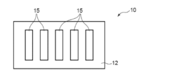
- (A)-(f) is sectional drawing which shows the manufacturing process of the high frequency ultrasonic piezoelectric element concerning the 1st Embodiment of this invention in order. It is a top view which shows the high frequency ultrasonic piezoelectric element which concerns on the 1st Embodiment of this invention. It is sectional drawing which shows the high frequency ultrasonic piezoelectric element which concerns on the modification of the 1st Embodiment of this invention. (A) is sectional drawing which shows the high frequency ultrasonic piezoelectric element which concerns on the 2nd Embodiment of this invention, (b) is a top view which shows the high frequency ultrasonic piezoelectric element which concerns on the 2nd Embodiment of this invention. is there.
- a plate-like flat lower electrode 11 is prepared.
- the material of the lower electrode 11 is not particularly limited as long as it is conductive and is usually made of a metal used as an electrode. Further, the thickness of the lower electrode 11 is not particularly limited, and may be appropriately selected from the viewpoint of miniaturization and strength of the piezoelectric element, and is, for example, 10 ⁇ m to 150 ⁇ m.
- a piezoelectric film 12 is formed on the lower electrode 11.
- the piezoelectric film 12 is obtained by applying a composite containing a sol-gel solution and a piezoelectric powder on the lower electrode 11 by a spraying method using a spray device, and sintering the applied composite.
- the sol-gel solution is obtained by dissolving a metal alkoxide in a solvent such as ethanol or methanol, and it is particularly preferable to use a PZT sol-gel solution containing lead alkoxide, zirconium alkoxide, and titanium alkoxide. Further, PZT can be used as the material of the piezoelectric powder.
- the particle size of the piezoelectric powder is preferably 50 to 1000 nm.
- the discharge amount of the composite by the spray method, the discharge time, the distance from the spray to the lower electrode, and the like can be appropriately changed according to the film thickness of the piezoelectric film to be formed. In order to obtain a piezoelectric element capable of transmitting and receiving ultrasonic waves of higher frequency, it is preferable to reduce the thickness of the piezoelectric film. By using the spray method, it is easy to control the discharge amount or discharge time of the composite.
- a composite layer having a thickness of about 10 ⁇ m can be formed under a discharge time condition of 200 ms. After application by this spray method, the composite layer is dried at about 150 ° C. for 5 minutes, pre-sintered at about 450 ° C. for 5 minutes, and fired at about 650 ° C. for 5 minutes, and then subjected to polarization treatment, for example, by corona discharge Thus, the piezoelectric film 12 is obtained.
- a mask layer 13 is disposed on the piezoelectric film 12.
- a material of the mask layer 13 for example, a material such as resin, glass, wood, or paper can be used, but is not limited thereto.
- a plurality of openings 14 exposing the piezoelectric film 12 are formed in the mask layer 13.
- the openings 14 are provided at desired positions where the upper electrode 15 will be formed later.
- the openings 14 are arranged at equal intervals along the length direction of the lower electrode.
- the opening 14 may be formed by chemical treatment such as an etching method or mechanical treatment such as cutting according to the material of the mask layer 13.
- the opening 14 is formed after the mask layer 13 is provided on the piezoelectric film 12.
- the opening 14 is previously formed in the mask layer 13 before being provided on the piezoelectric film 12.
- the mask layer 13 in which the opening 14 is formed may be disposed on the piezoelectric film 12.
- an upper electrode 15 is formed on the piezoelectric film 12 and the mask layer 13.
- the material of the upper electrode 15 is a conductive material and is not particularly limited as long as it can be used for an electrode.
- a metal such as gold or silver is used.
- the upper electrode 15 can be formed by a conventional method such as vapor deposition or sputtering.
- the thickness of the upper electrode 15 is not particularly limited, and may be appropriately selected from the viewpoint of miniaturization and strength of the piezoelectric element, and is, for example, 10 ⁇ m to 150 ⁇ m.
- the high-frequency ultrasonic piezoelectric element 10 can be obtained by connecting the lead wire connected to the power source to each of the lower electrode 11 and the plurality of upper electrodes 15 thereafter.
- the present invention is not limited to this, and the upper electrode 15 is formed as shown in FIG. Five or more desired numbers of upper electrodes 15 may be formed.
- a plurality of upper electrodes 15 are formed in an array on the piezoelectric film 12. Specifically, as shown in FIGS. 1 (f) and 2, the upper electrode 15 is the length of the lower electrode 11. It arrange
- the piezoelectric film positioned immediately below the plurality of upper electrodes A so-called phased array that can acquire a cross-sectional image of the inside of a living body by electronic scanning by controlling the timing at which a voltage is applied to the upper electrode so that each of the regions transmits ultrasonic waves at a specific time difference.
- a type of ultrasonic probe can be obtained.
- the high-frequency ultrasonic probe including the high-frequency ultrasonic piezoelectric element according to the present embodiment includes a backing material from the proximal end side toward the distal end side in the probe main body as in the conventional ultrasonic probe, the piezoelectric element according to the present embodiment, An acoustic matching layer and an acoustic lens are arranged in this order.
- the backing material and the acoustic matching layer are not essential components.
- a plurality of upper electrodes are formed using a mask having an opening on a piezoelectric film formed so as to cover the lower electrode, but an array is formed on the lower electrode.
- a plurality of piezoelectric films arranged in an array may be formed using a mask having openings formed in a shape, and an upper electrode may be formed on each of the plurality of piezoelectric films.
- a cutting process such as dicing the piezoelectric film in order to prevent crosstalk in the piezoelectric element. Absent.
- cutting a thin piezoelectric film is advantageous in this respect because it is difficult to cause cracks and the like.
- the high-frequency ultrasonic piezoelectric element 10 is manufactured using the plate-like flat lower electrode 11, but the plate-like lower electrode having a concave portion extending in the length direction on the surface thereof is used.
- a high-frequency ultrasonic piezoelectric element may be formed by forming a piezoelectric film and an upper electrode in the recess.
- Such a high-frequency ultrasonic piezoelectric element will be described as a modification of the first embodiment with reference to FIG. In the present embodiment, description of the same points as those in the first embodiment will be omitted, and only different points will be described in detail.
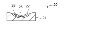
- FIG. 3 shows an ultrasonic piezoelectric element equivalent to the high-frequency ultrasonic piezoelectric element shown in FIG.
- the lower electrode has a recess.
- the length of the upper electrode on one upper electrode is shown.
- a cross section along the vertical direction is shown. That is, in the high-frequency ultrasonic piezoelectric element according to this modification, a plurality of upper electrodes are arranged along a direction perpendicular to the paper surface of FIG.
- the high-frequency ultrasonic piezoelectric element 20 includes a lower electrode 21 having a concave portion 26 formed on the surface thereof.
- the recess 26 is formed so as to extend along the length direction of the lower electrode 21.
- the peripheral edge of the opening of the recess 26 (the boundary between the surface of the lower electrode 21 and the recess 26) is rounded.
- a piezoelectric film 22 is formed on the bottom surface of the recess 26 of the lower electrode 21.
- the piezoelectric film 22 is formed along the bottom shape of the recess 26.
- An upper electrode 25 is formed on the piezoelectric film 22.
- a plurality of upper electrodes 25 are arranged along the length direction of the lower electrode 21, that is, along the direction in which the recesses extend.
- the high-frequency ultrasonic piezoelectric element 20 according to this modified example uses the high-frequency ultrasonic piezoelectric element 20 according to the above-described first embodiment except that the lower electrode 21 having the concave portions 26 is used. A method similar to that for the ultrasonic piezoelectric element 10 can be used.
- a plurality of piezoelectric films aligned along the direction in which the concave portion extends are formed on the lower electrode, and the upper electrode may be formed on each of the plurality of piezoelectric films.
- the piezoelectric film disposed in the concave portion 26 since the concave portion 26 extending in parallel with the arrangement direction of the piezoelectric films 22 is formed on the surface of the lower electrode 21, the piezoelectric film disposed in the concave portion 26.
- the ultrasonic wave transmitted from 22 can be converged while suppressing spreading in the direction perpendicular to the direction in which the recess 26 extends (the width direction of the lower electrode 21).
- this high-frequency ultrasonic piezoelectric element 20 is applied to an ultrasonic probe, it is not necessary to provide an acoustic lens.
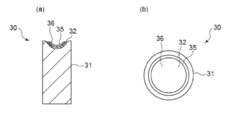
- the high-frequency ultrasonic piezoelectric element 30 according to a second embodiment of the present invention uses a rod-shaped lower electrode 31 as a lower electrode, and a single piezoelectric element. The formation of the film 32 and the upper electrode 35 is different.
- the lower electrode 31 has a rod shape as described above, and particularly a cylindrical shape. Further, a spherical recess 36 having a circular opening is formed on one end surface of the lower electrode 31. The peripheral edge of the opening of the recess 36 (the boundary between the surface of the lower electrode 31 and the recess 36) is rounded.
- the diameter of the cross section of the lower electrode 31 is 10 mm
- the opening diameter of the recess 36 is 6 mm
- the depth of the recess 36 is 2 mm.
- these sizes are merely examples, and the present invention is not limited to these sizes, and these sizes can be appropriately selected.
- a piezoelectric film 32 is formed on the bottom surface of the recess 36 of the lower electrode 31.
- the piezoelectric film 32 is formed along the bottom shape of the recess 36.
- the piezoelectric film 32 can be formed by applying and sintering a composite by a spray method.
- An upper electrode 35 is formed on the piezoelectric film 32.
- the upper electrode 35 is also formed along the bottom shape of the recess 36.
- the upper electrode 35 made of a single film is formed.
- the lower electrode 31 and the upper electrode 35 are connected to lead wires connected to a power source, respectively.
- the piezoelectric film 32 and the upper electrode 35 are formed on the end face of the rod-shaped lower electrode 31, so that this is a single vibrator type used for mechanical scanning. It can be applied to an ultrasonic probe.
- the high-frequency ultrasonic probe including the high-frequency ultrasonic piezoelectric element 30 according to this embodiment can have the same configuration as that of the first embodiment.
- the piezoelectric film 32 and the upper electrode 35 are formed in the recess 36 formed on the end surface of the rod-shaped lower electrode 31, so that the transmission from the piezoelectric film 32 is performed.
- the composite containing the sol-gel solution and the piezoelectric powder is applied on the lower electrode by the spray method. Therefore, an extremely thin piezoelectric film can be easily obtained, and as a result, a high-frequency ultrasonic probe that can transmit and receive higher-frequency ultrasonic waves and can acquire higher-definition images can be obtained.
Landscapes
- Engineering & Computer Science (AREA)
- Manufacturing & Machinery (AREA)
- Physics & Mathematics (AREA)
- Acoustics & Sound (AREA)
- Signal Processing (AREA)
- Chemical & Material Sciences (AREA)
- Dispersion Chemistry (AREA)
- Inorganic Chemistry (AREA)
- Ultra Sonic Daignosis Equipment (AREA)
- Transducers For Ultrasonic Waves (AREA)
- Investigating Or Analyzing Materials By The Use Of Ultrasonic Waves (AREA)
Applications Claiming Priority (2)
| Application Number | Priority Date | Filing Date | Title |
|---|---|---|---|
| JP2015-126268 | 2015-06-24 | ||
| JP2015126268A JP6122066B2 (ja) | 2015-06-24 | 2015-06-24 | 高周波超音波圧電素子、その製造方法、及びそれを含む高周波超音波プローブ |
Publications (1)
| Publication Number | Publication Date |
|---|---|
| WO2016208425A1 true WO2016208425A1 (ja) | 2016-12-29 |
Family
ID=57584920
Family Applications (1)
| Application Number | Title | Priority Date | Filing Date |
|---|---|---|---|
| PCT/JP2016/067395 Ceased WO2016208425A1 (ja) | 2015-06-24 | 2016-06-10 | 高周波超音波圧電素子、その製造方法、及びそれを含む高周波超音波プローブ |
Country Status (3)
| Country | Link |
|---|---|
| JP (1) | JP6122066B2 (enExample) |
| TW (1) | TWI693731B (enExample) |
| WO (1) | WO2016208425A1 (enExample) |
Cited By (1)
| Publication number | Priority date | Publication date | Assignee | Title |
|---|---|---|---|---|
| EP4468743A4 (en) * | 2022-01-19 | 2026-01-07 | Cast Inc | ULTRASONIC PROBE AND METHOD FOR MANUFACTURING ULTRASONIC PROBE |
Families Citing this family (1)
| Publication number | Priority date | Publication date | Assignee | Title |
|---|---|---|---|---|
| KR101965171B1 (ko) * | 2018-08-24 | 2019-08-13 | (주)비티비엘 | 초음파센서의 제조방법 |
Citations (6)
| Publication number | Priority date | Publication date | Assignee | Title |
|---|---|---|---|---|
| JPH01171200U (enExample) * | 1988-05-10 | 1989-12-04 | ||
| JP2002008939A (ja) * | 2000-04-13 | 2002-01-11 | Fujitsu Ltd | 選択的コーティングによるセラミック体の製造方法 |
| JP2008535643A (ja) * | 2005-03-02 | 2008-09-04 | リサーチ・トライアングル・インスティチュート | 空気に支持されたキャビティを有する圧電微小加工超音波振動子 |
| JP2012011024A (ja) * | 2010-07-01 | 2012-01-19 | Konica Minolta Medical & Graphic Inc | 超音波探触子、および超音波診断装置 |
| JP2013168573A (ja) * | 2012-02-16 | 2013-08-29 | Mitsubishi Heavy Ind Ltd | 超音波厚みセンサの製造方法 |
| JP2014212872A (ja) * | 2013-04-24 | 2014-11-17 | 国立大学法人電気通信大学 | 超音波診断装置及び超音波画像構築方法 |
Family Cites Families (5)
| Publication number | Priority date | Publication date | Assignee | Title |
|---|---|---|---|---|
| JP4759117B2 (ja) * | 2000-06-22 | 2011-08-31 | 日本特殊陶業株式会社 | 金属酸化物膜付き基板及び金属酸化物膜付き基板の製造方法 |
| JP2004111835A (ja) * | 2002-09-20 | 2004-04-08 | Canon Inc | 圧電体素子の製造方法、圧電体素子及びインクジェット式記録ヘッド |
| JP2005327919A (ja) * | 2004-05-14 | 2005-11-24 | Seiko Epson Corp | デバイスの製造方法及びデバイス、電気光学素子、プリンタ |
| JP5540361B2 (ja) * | 2011-06-07 | 2014-07-02 | 日立Geニュークリア・エナジー株式会社 | 超音波センサ及びその製造方法 |
| JP2013207155A (ja) * | 2012-03-29 | 2013-10-07 | Mitsubishi Materials Corp | 強誘電体薄膜の製造方法 |
-
2015
- 2015-06-24 JP JP2015126268A patent/JP6122066B2/ja active Active
-
2016
- 2016-06-10 WO PCT/JP2016/067395 patent/WO2016208425A1/ja not_active Ceased
- 2016-06-21 TW TW105119414A patent/TWI693731B/zh not_active IP Right Cessation
Patent Citations (6)
| Publication number | Priority date | Publication date | Assignee | Title |
|---|---|---|---|---|
| JPH01171200U (enExample) * | 1988-05-10 | 1989-12-04 | ||
| JP2002008939A (ja) * | 2000-04-13 | 2002-01-11 | Fujitsu Ltd | 選択的コーティングによるセラミック体の製造方法 |
| JP2008535643A (ja) * | 2005-03-02 | 2008-09-04 | リサーチ・トライアングル・インスティチュート | 空気に支持されたキャビティを有する圧電微小加工超音波振動子 |
| JP2012011024A (ja) * | 2010-07-01 | 2012-01-19 | Konica Minolta Medical & Graphic Inc | 超音波探触子、および超音波診断装置 |
| JP2013168573A (ja) * | 2012-02-16 | 2013-08-29 | Mitsubishi Heavy Ind Ltd | 超音波厚みセンサの製造方法 |
| JP2014212872A (ja) * | 2013-04-24 | 2014-11-17 | 国立大学法人電気通信大学 | 超音波診断装置及び超音波画像構築方法 |
Non-Patent Citations (1)
| Title |
|---|
| MAKIKO KOBAYASHI: "Sol-gel composite ultrasonic transducers", JOURNAL OF THE ACOUSTICAL SOCIETY OF JAPAN, vol. 71, no. 5, pages 253 - 259 * |
Cited By (1)
| Publication number | Priority date | Publication date | Assignee | Title |
|---|---|---|---|---|
| EP4468743A4 (en) * | 2022-01-19 | 2026-01-07 | Cast Inc | ULTRASONIC PROBE AND METHOD FOR MANUFACTURING ULTRASONIC PROBE |
Also Published As
| Publication number | Publication date |
|---|---|
| TW201705560A (zh) | 2017-02-01 |
| TWI693731B (zh) | 2020-05-11 |
| JP2017011144A (ja) | 2017-01-12 |
| JP6122066B2 (ja) | 2017-04-26 |
Similar Documents
| Publication | Publication Date | Title |
|---|---|---|
| US11759175B2 (en) | Configurable ultrasonic imager | |
| US9812634B2 (en) | Method of making thick film transducer arrays | |
| US7449821B2 (en) | Piezoelectric micromachined ultrasonic transducer with air-backed cavities | |
| JP2000050391A (ja) | 超音波トランスデューサーおよびその製造方法 | |
| CN107534815B (zh) | 包括具有复合结构的匹配层的超声换能器及其制造方法 | |
| CN1863485A (zh) | 超声波探头、超声波成像设备以及超声波成像方法 | |
| US20100001619A1 (en) | Perovskite-type oxide single crystal and method of manufacturing the same, composite piezoelectric material, piezoelectric vibrator, ultrasonic probe, and ultrasonic diagnostic apparatus | |
| EP2902118A2 (en) | Ultrasonic device, probe, electronic device, and ultrasound imaging apparatus | |
| Tipsawat et al. | 32 element piezoelectric micromachined ultrasound transducer (PMUT) phased array for neuromodulation | |
| JP2000028595A (ja) | 圧電構造体の製造方法および複合圧電振動子 | |
| JP2000300559A (ja) | 超音波探触子及びその製造方法 | |
| US20100001620A1 (en) | Microstructure of perovskite-type oxide single crystal and method of manufacturing the same, composite piezoelectric material, piezoelectric vibrator, ultrasonic probe, and ultrasonic diagnostic apparatus | |
| JP6122066B2 (ja) | 高周波超音波圧電素子、その製造方法、及びそれを含む高周波超音波プローブ | |
| US20050179345A1 (en) | Piezoelectric element and method of manufacturing the same | |
| JP4528606B2 (ja) | 超音波プローブ及び超音波診断装置 | |
| JPH11285096A (ja) | 複合圧電振動子 | |
| JP5794114B2 (ja) | 圧電素子およびその製造方法と、超音波送受信プローブ | |
| KR102000689B1 (ko) | 원심 패턴 충진 장치 및 이를 이용한 초음파 압전 센서의 제조 방법, 그리고 이러한 방법으로 제조된 초음파 압전 센서 혹은 초음파 인식 센서 | |
| JP2008048276A (ja) | 超音波トランスデューサ及び超音波トランスデューサアレイ | |
| JP2013026682A (ja) | 医用複合単結晶圧電振動子、医用超音波プローブ、医用複合単結晶圧電振動子製造方法および医用超音波プローブ製造方法 | |
| TW202312524A (zh) | 具絕緣層之微機械超音波傳感器及製造方法 | |
| JP2024528548A (ja) | 絶縁層を伴う微小機械加工超音波トランスデューサ、および、製造の方法 | |
| JP2003174698A (ja) | 複合圧電体およびその製造方法 | |
| JP7666048B2 (ja) | 電気機械変換素子、超音波トランスデューサ、超音波探触子、超音波診断装置 | |
| Wu et al. | High-frequency piezoelectric PZT film micromachined ultrasonic arrays |
Legal Events
| Date | Code | Title | Description |
|---|---|---|---|
| 121 | Ep: the epo has been informed by wipo that ep was designated in this application |
Ref document number: 16814196 Country of ref document: EP Kind code of ref document: A1 |
|
| NENP | Non-entry into the national phase |
Ref country code: DE |
|
| 122 | Ep: pct application non-entry in european phase |
Ref document number: 16814196 Country of ref document: EP Kind code of ref document: A1 |