WO2016208119A1 - 光走査装置 - Google Patents
光走査装置 Download PDFInfo
- Publication number
- WO2016208119A1 WO2016208119A1 PCT/JP2016/002527 JP2016002527W WO2016208119A1 WO 2016208119 A1 WO2016208119 A1 WO 2016208119A1 JP 2016002527 W JP2016002527 W JP 2016002527W WO 2016208119 A1 WO2016208119 A1 WO 2016208119A1
- Authority
- WO
- WIPO (PCT)
- Prior art keywords
- angular velocity
- mirror
- optical scanning
- scanning device
- target
- Prior art date
- Legal status (The legal status is an assumption and is not a legal conclusion. Google has not performed a legal analysis and makes no representation as to the accuracy of the status listed.)
- Ceased
Links
Images


Classifications
-
- B—PERFORMING OPERATIONS; TRANSPORTING
- B06—GENERATING OR TRANSMITTING MECHANICAL VIBRATIONS IN GENERAL
- B06B—METHODS OR APPARATUS FOR GENERATING OR TRANSMITTING MECHANICAL VIBRATIONS OF INFRASONIC, SONIC, OR ULTRASONIC FREQUENCY, e.g. FOR PERFORMING MECHANICAL WORK IN GENERAL
- B06B1/00—Methods or apparatus for generating mechanical vibrations of infrasonic, sonic, or ultrasonic frequency
- B06B1/02—Methods or apparatus for generating mechanical vibrations of infrasonic, sonic, or ultrasonic frequency making use of electrical energy
- B06B1/06—Methods or apparatus for generating mechanical vibrations of infrasonic, sonic, or ultrasonic frequency making use of electrical energy operating with piezoelectric effect or with electrostriction
- B06B1/0607—Methods or apparatus for generating mechanical vibrations of infrasonic, sonic, or ultrasonic frequency making use of electrical energy operating with piezoelectric effect or with electrostriction using multiple elements
-
- G—PHYSICS
- G02—OPTICS
- G02B—OPTICAL ELEMENTS, SYSTEMS OR APPARATUS
- G02B26/00—Optical devices or arrangements for the control of light using movable or deformable optical elements
- G02B26/08—Optical devices or arrangements for the control of light using movable or deformable optical elements for controlling the direction of light
-
- G—PHYSICS
- G02—OPTICS
- G02B—OPTICAL ELEMENTS, SYSTEMS OR APPARATUS
- G02B26/00—Optical devices or arrangements for the control of light using movable or deformable optical elements
- G02B26/08—Optical devices or arrangements for the control of light using movable or deformable optical elements for controlling the direction of light
- G02B26/0816—Optical devices or arrangements for the control of light using movable or deformable optical elements for controlling the direction of light by means of one or more reflecting elements
- G02B26/0833—Optical devices or arrangements for the control of light using movable or deformable optical elements for controlling the direction of light by means of one or more reflecting elements the reflecting element being a micromechanical device, e.g. a MEMS mirror, DMD
-
- G—PHYSICS
- G02—OPTICS
- G02B—OPTICAL ELEMENTS, SYSTEMS OR APPARATUS
- G02B26/00—Optical devices or arrangements for the control of light using movable or deformable optical elements
- G02B26/08—Optical devices or arrangements for the control of light using movable or deformable optical elements for controlling the direction of light
- G02B26/0816—Optical devices or arrangements for the control of light using movable or deformable optical elements for controlling the direction of light by means of one or more reflecting elements
- G02B26/0833—Optical devices or arrangements for the control of light using movable or deformable optical elements for controlling the direction of light by means of one or more reflecting elements the reflecting element being a micromechanical device, e.g. a MEMS mirror, DMD
- G02B26/0858—Optical devices or arrangements for the control of light using movable or deformable optical elements for controlling the direction of light by means of one or more reflecting elements the reflecting element being a micromechanical device, e.g. a MEMS mirror, DMD the reflecting means being moved or deformed by piezoelectric means
-
- G—PHYSICS
- G02—OPTICS
- G02B—OPTICAL ELEMENTS, SYSTEMS OR APPARATUS
- G02B26/00—Optical devices or arrangements for the control of light using movable or deformable optical elements
- G02B26/08—Optical devices or arrangements for the control of light using movable or deformable optical elements for controlling the direction of light
- G02B26/10—Scanning systems
-
- G—PHYSICS
- G02—OPTICS
- G02B—OPTICAL ELEMENTS, SYSTEMS OR APPARATUS
- G02B26/00—Optical devices or arrangements for the control of light using movable or deformable optical elements
- G02B26/08—Optical devices or arrangements for the control of light using movable or deformable optical elements for controlling the direction of light
- G02B26/10—Scanning systems
- G02B26/101—Scanning systems with both horizontal and vertical deflecting means, e.g. raster or XY scanners
-
- H—ELECTRICITY
- H10—SEMICONDUCTOR DEVICES; ELECTRIC SOLID-STATE DEVICES NOT OTHERWISE PROVIDED FOR
- H10N—ELECTRIC SOLID-STATE DEVICES NOT OTHERWISE PROVIDED FOR
- H10N30/00—Piezoelectric or electrostrictive devices
- H10N30/704—Piezoelectric or electrostrictive devices based on piezoelectric or electrostrictive films or coatings
-
- B—PERFORMING OPERATIONS; TRANSPORTING
- B81—MICROSTRUCTURAL TECHNOLOGY
- B81B—MICROSTRUCTURAL DEVICES OR SYSTEMS, e.g. MICROMECHANICAL DEVICES
- B81B3/00—Devices comprising flexible or deformable elements, e.g. comprising elastic tongues or membranes
- B81B3/0018—Structures acting upon the moving or flexible element for transforming energy into mechanical movement or vice versa, i.e. actuators, sensors, generators
- B81B3/0021—Transducers for transforming electrical into mechanical energy or vice versa
-
- H—ELECTRICITY
- H10—SEMICONDUCTOR DEVICES; ELECTRIC SOLID-STATE DEVICES NOT OTHERWISE PROVIDED FOR
- H10N—ELECTRIC SOLID-STATE DEVICES NOT OTHERWISE PROVIDED FOR
- H10N30/00—Piezoelectric or electrostrictive devices
- H10N30/80—Constructional details
- H10N30/85—Piezoelectric or electrostrictive active materials
- H10N30/853—Ceramic compositions
- H10N30/8548—Lead-based oxides
- H10N30/8554—Lead-zirconium titanate [PZT] based
Definitions
- This disclosure relates to a two-axis optical scanning device.
- an optical scanning device such as a laser scanning module that draws an arbitrary image on a screen by two-dimensionally scanning laser light generated by an RGB (Red Green Blue) light source using a MEMS (Micro Electro Mechanical Systems) mirror has been proposed.
- RGB Red Green Blue
- MEMS Micro Electro Mechanical Systems
- Such an optical scanning device includes a mirror, a support beam that supports both mirrors, a resonance drive unit that supports the mirror via the support beam, and a forced drive unit that supports the resonance drive unit.
- the optical scanning device rotates the mirror around two axes perpendicular to each other by applying a voltage to the piezoelectric films provided in the resonance driving unit and the forcible driving unit, and two-dimensionally changes the imaging position by the mirror. Scanning is possible.
- the rotation of the mirror by the forcible drive unit is slower than the rotation by the resonance drive unit, and the waveform of the voltage applied to the piezoelectric film provided in the forcible drive unit is a sawtooth waveform.
- the resonance component included in the harmonics of the sawtooth wave may cause the mirror to resonate and generate unnecessary vibration called ringing.
- the frequency of the resonance component that causes ringing varies depending on the temperature, the acceleration that the mirror receives, and the deterioration of the mirror. For example, when an optical scanning device is mounted on a vehicle, this frequency is large and fluctuates rapidly.
- the image of the drive signal is not a sawtooth wave but a sine wave during the detection, so that a normal image cannot be drawn. Therefore, it is necessary to stop drawing the video while detecting the ringing frequency.
- an object of the present disclosure to provide an optical scanning device capable of detecting a ringing frequency even during scanning.
- an optical scanning device includes a mirror that reflects a light beam on a reflection surface, and extends on both sides in one direction on a plane of the reflection surface, and supports both mirrors.
- a support beam a resonance drive unit that causes the mirror to swing around a first axis parallel to one direction by resonantly vibrating the support beam, and a direction different from the one direction by applying a voltage to the piezoelectric element.
- a forcible drive unit that swings around the second axis facing, an angle measurement unit that measures an angle around the second axis of the mirror, and a control circuit that applies a voltage according to the output of the angle measurement unit to the piezoelectric element.
- the control circuit includes an angular velocity calculator that calculates an angular velocity around the second axis of the mirror based on the angle of the mirror measured by the angle measurement unit, a target angular velocity calculator that calculates a target value of the angular velocity, an angular velocity and a target value.
- a resonance frequency detector for detecting a vibration frequency around the second axis of the mirror, a drive waveform generator for generating a sawtooth drive signal, and a vibration frequency of the mirror detected by the resonance frequency detector.
- an unnecessary vibration controller that optimizes the drive signal so as to reduce unnecessary vibration around the second axis of the mirror and applies a voltage corresponding to the optimized drive signal to the piezoelectric element.
- the resonance frequency detector detects the vibration frequency of the mirror using the waveform of the angular velocity of the mirror and the target value during the period in which the sawtooth drive signal is sent from the drive waveform generator to the unnecessary vibration controller.
- the resonance frequency detector uses the mirror angular velocity waveform and the target value during the period in which the sawtooth drive signal is sent from the drive waveform generator to the unnecessary vibration controller, and calculates the vibration frequency of the mirror. To detect. Therefore, the ringing frequency can be detected even during scanning.
- the optical scanning device 100 is a two-axis optical scanning device that rotates a MEMS mirror around two axes perpendicular to each other so that an imaging position by the MEMS mirror can be scanned two-dimensionally.
- the optical scanning device 100 includes a reflection unit 1, a light source 2, and a control circuit 3, and controls the actuator provided in the reflection unit 1 by the control circuit 3.
- An image is drawn on the screen 200 by reflecting the beam by the reflection unit 1.
- the reflection part 1 reflects the light beam irradiated from the light source 2, and as shown in FIG. 2, the mirror 11, the support beam 12, the resonance drive part 13, the connection part 14, and a forced drive part. 15, a support portion 16, and an angle sensor 17.
- FIG. 2 is not a cross-sectional view, hatching is performed on a reflective surface 11a, a piezoelectric element 132, a wiring 133, pads 134a and 134b, and a piezoelectric element 152, which will be described later, in order to make the drawing easier to see.
- the substrate 10 is configured by an SOI (Silicon on Insulator) substrate having a structure in which an active layer, a BOX layer (buried oxide layer) and a support layer are sequentially stacked.
- the active layer is made of, for example, Si
- the BOX layer is made of, for example, SiO2
- the support layer is made of, for example, Si.
- the active layer is patterned on the above-described constituent elements included in the reflection portion 1.
- the mirror 11 reflects the light beam applied to the reflection unit 1.
- the mirror 11 is a portion formed by patterning the active layer of the substrate 10 in a circular shape. As shown in FIG. 2, a reflective surface 11a made of Al or the like is formed on the upper surface of the mirror 11. Yes.
- the one direction in the plane of the reflective surface 11a is defined as the x direction, and the direction perpendicular to the x direction in the plane of the reflective surface 11a is defined as the y direction.
- the mirror 11 is supported at both ends by support beams 12 extending on both sides in the x direction around the mirror 11.
- the support beam 12 enables the mirror 11 to swing around an axis A1 parallel to the x direction.
- the mirror 11 is supported by the resonance driving unit 13 via the support beam 12.
- the resonance driving unit 13 swings the mirror 11 about the axis A1 by causing the support beam 12 to resonate and vibrate.
- the axis A1 corresponds to the first axis.
- the resonance driving unit 13 is configured by forming four piezoelectric elements 132 and wirings 133 on the upper surface of a rectangular frame 131 formed by patterning the active layer of the substrate 10.
- the support beam 12 is connected to the center of each of two opposing sides of the frame 131.
- the piezoelectric element 132 has a structure in which a lower electrode, a piezoelectric film, and an upper electrode are sequentially stacked.
- the lower electrode and the upper electrode are made of, for example, Al, Au, Pt or the like.
- the piezoelectric film is made of a piezoelectric material such as lead zirconate titanate (PZT).
- PZT lead zirconate titanate
- the lower electrode and the upper electrode may have a Pt / Ti laminated structure.
- the piezoelectric elements 132 are piezoelectric elements 132a, 132b, 132c, and 132d, as shown in FIG. 2, the piezoelectric elements 132a and 132b are disposed on one side of the axis A1, and the piezoelectric elements 132c and 132d are disposed on the other side.
- piezoelectric elements 132a and 132c are arranged on one side of the mirror 11 in the x direction
- piezoelectric elements 132b and 132d are arranged on the other side.
- the wiring 133 has a structure in which a lower wiring, an insulating film, and an upper wiring are laminated in order, and is divided into four wirings 133a, 133b, 133c, and 133d as shown in FIG.
- the lower wiring and the upper wiring are made of, for example, Al, Au, Pt, etc., like the lower electrode and the upper electrode of the piezoelectric element 132.
- the insulating film is made of, for example, lead zirconate titanate (PZT).
- the lower wiring and the upper wiring may have a Pt / Ti laminated structure.
- the wiring 133a is formed on the upper surface of the frame 131, and electrically connects the piezoelectric element 132a and the piezoelectric element 132b.
- the wiring 133b is formed on the upper surface of the frame 131, and electrically connects the piezoelectric element 132c and the piezoelectric element 132d.
- the wirings 133c and 133d connect the piezoelectric elements 132a and 132c to the pads 134a and 134b formed on the upper surface of the support portion 16, respectively, and are connected from the frame 131 to the connecting portion of the upper surface of the active layer of the substrate 10. 14, the force drive unit 15, and the support unit 16 are formed in the part.
- the pads 134 a and 134 b are connected to the control circuit 3.
- the connecting portion 14 extends from one end portion in the x direction to the outside in the y direction in the frame 131.
- the connecting portion 14 is connected to the forcible driving portion 15 at the end opposite to the frame 131.
- the forcible drive unit 15 swings the mirror 11 about the axis A2 parallel to the y direction by swinging the frame 131 about the axis parallel to the y direction through the connecting unit 14.
- the axis A2 corresponds to the second axis.
- the forced drive unit 15 is configured by forming two piezoelectric elements 152 on the upper surface of a base 151 formed by patterning the active layer of the substrate 10.
- the base 151 is disposed on both sides of the mirror 11 in the y direction, extends in the x direction, is connected to the connecting portion 14 at one end in the x direction, and is connected to the other side. The end portion is connected to the support portion 16.
- a portion disposed on the same side in the y direction as the piezoelectric elements 132a and 132b with respect to the mirror 11 is defined as a base 151a
- a portion disposed on the same side as the piezoelectric elements 132c and 132d is defined as a base 151b.
- the piezoelectric element 152 has a structure in which a lower electrode, a piezoelectric film, and an upper electrode are sequentially stacked.
- the lower electrode and the upper electrode are made of, for example, Al, Au, Pt or the like.
- the piezoelectric film is made of a piezoelectric material such as lead zirconate titanate (PZT).
- PZT lead zirconate titanate
- the lower electrode and the upper electrode may have a Pt / Ti laminated structure.
- the two piezoelectric elements 152 are referred to as piezoelectric elements 152a and 152b, respectively. As shown in FIG. 2, the piezoelectric elements 152a and 152b are formed on the upper surfaces of the bases 151a and 151b, respectively, and from the end of the upper surfaces of the bases 151a and 151b on the connecting portion 14 side, It is formed to reach the upper surface of.
- the piezoelectric elements 152 a and 152 b are connected to the control circuit 3.
- a portion of the upper surface of the base portion 151a closer to the mirror 11 than the piezoelectric element 152a in the y direction and a portion of the upper surface of the base portion 151b closer to the mirror 11 than the piezoelectric element 152b in the y direction are respectively connected from the connecting portion 14 to the support portion.
- Wirings 133c and 133d extending to 16 are formed.
- the support unit 16 supports the mirror 11 via the support beam 12, the resonance drive unit 13, the connection unit 14, and the forced drive unit 15.
- part of the wirings 133 c and 133 d, the pads 134 a and 134 b, and part of the piezoelectric elements 152 a and 152 b of the resonance driving unit 13 and the forced driving unit 15 are formed on the upper surface of the support unit 16.
- the angle sensor 17 measures the angles around the axis A1 and the axis A2 of the mirror 11, and is composed of, for example, a strain gauge.
- the angle sensor 17a is installed on the upper surface of the support beam 12, and each of the angle sensors 17b and 17c is piezoelectric. It is installed on the upper surface of the elements 152a and 152b.
- the angle sensors 17a, 17b, and 17c are connected to the control circuit 3 through wiring not shown.
- the angle sensor 17a outputs a signal according to the angle around the axis A1 of the mirror 11, and the output of the angle sensor 17a is used for resonance drive control by the resonance drive unit 13.
- the angle sensors 17b and 17c output signals according to the angle around the axis A2 of the mirror 11, and the outputs of the angle sensors 17b and 17c are used for controlling the forced drive by the forced drive unit 15 in the operation of FIG. Used.
- the angle sensors 17b and 17c correspond to an angle measuring unit.
- the reflecting portion 1 is configured.
- Such a reflection portion 1 is formed by forming each piezoelectric element, each wiring, each pad, the reflecting surface 11a, and the angle sensor 17 on the surface of the active layer by photolithography and etching, and patterning the substrate 10 to form the mirror 11 and the like. It can manufacture by forming like.
- the light source 2 is an RGB laser unit that irradiates the reflection unit 1 with a light beam.
- the light source 2 is connected to the control circuit 3 as shown in FIG. 1, and changes the color of the light beam to be irradiated based on the signal from the control circuit 3.
- the control circuit 3 generates drive signals for the resonance drive unit 13 and the forcible drive unit 15 according to the output of the angle sensor 17, and applies voltages corresponding to the drive signals to the piezoelectric elements included in the resonance drive unit 13 and the forcible drive unit 15. To be applied.
- the control circuit 3 controls the light source 2.
- the control circuit 3 is also referred to as an electronic control unit.
- the control circuit 3 includes a microcomputer including a CPU, a storage unit such as a ROM and a RAM, and peripheral circuits thereof.
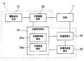
- Generator 31 also referred to as drive waveform generation unit 31
- unnecessary vibration controller 32 also referred to as unnecessary vibration control unit 32
- resonance characteristic detector 33 also referred to as resonance characteristic detection unit 33
- angular velocity A calculator 34 also referred to as an angular velocity calculator 34
- a target angular velocity calculator 35 also referred to as a target angular velocity calculator 35.
- These components can be realized by the CPU executing software stored in a ROM or the like, but some or all of the components may be realized as hardware.
- the drive waveform generator 31 generates a sawtooth drive signal in which a portion in which the magnitude of the signal decreases and a portion in which the amount of increase is the same as the amount of decrease in a time shorter than the time required for the reduction are alternately repeated. It is.
- the drive waveform generator 31 generates a sawtooth drive signal as a synthesized wave by synthesizing a plurality of sine waves having different frequencies. As shown in FIG. 3, the drive waveform generator 31 is connected to the unnecessary vibration controller 32, and the drive signal generated by the drive waveform generator 31 is sent to the unnecessary vibration controller 32.
- the unnecessary vibration controller 32 optimizes the drive signal so as to reduce the ringing around the axis A2 of the mirror 11 based on the ringing characteristics of the mirror 11, for example, the frequency.
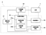
- the unnecessary vibration controller 32 is connected to the resonance characteristic detector 33 as shown in FIG. 3, and causes ringing based on the vibration frequency of the mirror 11 detected by the resonance characteristic detector 33. Is removed from the drive signal by a notch filter.
- the unnecessary vibration controller 32 is connected to the reflection unit 1.
- the control circuit 3 applies a voltage corresponding to the drive signal optimized by the unnecessary vibration controller 32 to the piezoelectric element 152 included in the forced drive unit 15 of the reflection unit 1.
- the resonance characteristic detector 33 detects the ringing characteristic of the mirror 11, and includes a resonance frequency detector 33a and a resonance intensity detector 33b as shown in FIG.
- the resonance frequency detector 33a detects the ringing frequency of the mirror 11.
- the resonance frequency detector 33a uses the angular velocity waveform of the mirror 11 and the target value of the angular velocity during the period in which a sawtooth drive signal is sent from the drive waveform generator 31 to the unnecessary vibration controller 32.
- the ringing frequency around 11 axes A2 is detected.
- the resonance intensity detector 33b detects the ringing intensity of the mirror 11.
- the resonance intensity detector 33b detects the intensity of ringing by comparing the angular velocity of the mirror 11 calculated by the angular velocity calculator 34 with the target value of the angular velocity of the mirror 11 calculated by the target angular velocity calculator 35.
- the resonance characteristic detector 33 sends a signal corresponding to the detected ringing frequency and intensity of the mirror 11 to the unnecessary vibration controller 32.
- the angular velocity calculator 34 calculates the angular velocity around the axis A2 of the mirror 11 based on the angle of the mirror 11 measured by the angle sensors 17b and 17c of the reflector 1. As shown in FIG. 3, the angular velocity calculator 34 is connected to the resonance characteristic detector 33 and the target angular velocity calculator 35, and a signal corresponding to the calculated angular velocity of the mirror 11 is sent to the resonance characteristic detector 33 and the target angular velocity calculator. Send to 35.
- the target angular velocity calculator 35 calculates the target value of the angular velocity around the axis A2 of the mirror 11 in the drawing section. In the present embodiment, the target angular velocity calculator 35 calculates the average value of the angular velocities of the mirror 11 calculated by the angular velocity calculator 34 in the drawing section, and sets it as the target value.
- the drawing section is a waveform obtained by optimizing the sawtooth drive signal generated by the drive waveform generator 31 by the unnecessary vibration controller 32, and the magnitude of change with respect to time is centered on a constant value. It is a straight section within a predetermined range.
- the target angular velocity calculator 35 calculates the average value of the angular velocities of the mirror 11 to obtain a target value
- the magnitude of the change with respect to time is constant in the waveform obtained by optimizing the drive signal by the unnecessary vibration controller 32.
- a linear section in which the magnitude of change with respect to time is constant is used for drawing in order to make the luminance constant. Therefore, by calculating the average value of the angular velocities calculated by the angular velocity calculator 34 in the drawing section as a target value, it is possible to easily detect the ringing characteristics without sending a signal other than the sawtooth wave to the unnecessary vibration controller 32. be able to.
- the mirror 11 is swung in the H direction in FIGS. 1 and 2 by the resonance driving unit 13 and is swung in the V direction in FIGS. 1 and 2 by the forced driving unit 15. Further, in the swing in the V direction, the mirror 11 swings at a low speed in one direction and then swings at a high speed in the other direction.
- the drawing section is a section corresponding to the case where the mirror 11 moves at low speed in the V direction while reflecting the light beam from the light source 2 in the graph of the angular velocity of the mirror 11.
- the target angular velocity calculator 35 is connected to the resonance characteristic detector 33 as shown in FIG. 3 and sends a signal corresponding to the calculated target value of the angular velocity of the mirror 11 to the resonance characteristic detector 33.
- the piezoelectric film included in the piezoelectric element 132 is deformed by applying a resonance scanning voltage to the electrode of the piezoelectric element 132 included in the resonance driving unit 13, and the support beam 12. Is resonantly oscillated. As a result, the mirror 11 is swung around the axis of the support beam 12.
- the piezoelectric film included in the piezoelectric element 152 is deformed, and the resonance driving unit 13 is moved around an axis parallel to the y direction. Rock.
- voltages having the same waveform are applied to the piezoelectric elements 152a and 152b.
- the mirror 11 is swung around the axis A1 parallel to the x direction and the axis A2 parallel to the y direction. Then, the light source 2 irradiates the mirror 11 with a light beam having a color corresponding to a signal from the control circuit 3, thereby enabling two-dimensional scanning.
- the forced scanning voltage applied from the control circuit 3 to the forced drive unit 15 is a voltage corresponding to a sawtooth drive signal.
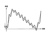
- the forced scanning voltage causes the mirror 11 to oscillate as indicated by the broken line in FIG. 4, that is, it is desirable that the graph of the angle with respect to time has a sawtooth waveform, but actually, as indicated by the solid line in FIG. In some cases, ringing is included in the movement of the mirror 11.
- the ringing of the mirror 11 is caused by a resonance component included in the drive signal.
- a method for removing the resonance component from the drive signal and suppressing the ringing of the mirror 11 will be described.
- the described flowchart includes a plurality of sections (or referred to as steps), and each section is expressed as S101, for example. Further, each section can be divided into a plurality of subsections, while a plurality of sections can be combined into one section.
- Each section can be referred to as a device or name with a structural modifier, for example, a detection section can be referred to as a detection device or a resonant frequency detector (detector).
- the section includes not only (i) a software section combined with a hardware unit (eg, a computer) but also (ii) a hardware (eg, integrated circuit, wiring logic circuit) section. As mentioned above, it can be realized with or without the function of the related device.
- the hardware section can be included inside the microcomputer.
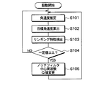
- the control circuit 3 performs the operation shown in the flowchart of FIG. 5 and suppresses the ringing of the mirror 11. First, when driving of the optical scanning device 100 is started, the control circuit 3 estimates the angular velocity of the mirror 11 in S101.
- the angular velocity calculator 34 acquires signals from the angle sensors 17b and 17c over a predetermined period including the drawing section, and calculates the angle of the mirror 11 using the acquired signals. Then, the angular velocity of the mirror 11 is obtained by differentiating the calculated angle. In this embodiment, the time difference between the sampling points of the calculated angle is taken as the angular velocity of the mirror 11.
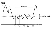
- the solid line in FIG. 6 indicates the angular velocity of the mirror 11 estimated by the angular velocity calculator 34.
- the control circuit 3 proceeds to S102.
- the control circuit 3 calculates the target value of the angular velocity of the mirror 11 based on the outputs of the angle sensors 17b and 17c. Specifically, the target angular velocity calculator 35 calculates the average value of the portion included in the drawing section in the angular velocity data of the mirror 11 estimated by the angular velocity calculator 34 and sets it as the target value of the angular velocity of the mirror 11. A broken line in FIG. 6 indicates a target value of the angular velocity calculated by the target angular velocity calculator 35. After calculating the target value of the angular velocity of the mirror 11, the control circuit 3 proceeds to S103.
- the control circuit 3 detects the ringing characteristic.
- the resonance frequency detector 33a of the resonance characteristic detector 33 uses the mirror 11 based on the time difference between two times when the angular velocity calculated by the angular velocity calculator 34 and the target value calculated by the target angular velocity calculator 35 coincide. The frequency of vibration is detected. Specifically, the intersection in the drawing section between the graph of the angular velocity of the mirror 11 estimated by the angular velocity calculator 34 and the target value of the angular velocity calculated by the target angular velocity calculator 35 is obtained. Then, the time difference between two adjacent intersections across one intersection is obtained, and the average value of the reciprocal of the obtained time difference is set as the ringing frequency.
- the time difference between two intersections adjacent to each other with respect to one intersection is, for example, the time difference between time points T1 and T2, T2 and T3, T3 and T4, and T4 and T5 in FIG.
- the resonance intensity detector 33b of the resonance characteristic detector 33 detects the ringing intensity. Specifically, in the graph of the angular velocity of the mirror 11 estimated by the angular velocity calculator 34, the maximum value and the minimum value of the angular velocity in the drawing section are obtained, and the difference between the maximum value and the minimum value is set as the ringing intensity.
- the control circuit 3 When detecting the ringing characteristic, the control circuit 3 proceeds to S104 and determines whether or not the drive signal needs to be optimized based on the ringing characteristic. Specifically, the control circuit 3 determines whether or not the ringing intensity obtained in S103 is equal to or greater than a certain value. If the ringing intensity is not greater than or equal to a certain value, the control circuit 3 proceeds to S101. If the ringing intensity is greater than or equal to a certain value, the control circuit 3 proceeds to S105.
- the control circuit 3 optimizes the drive signal based on the ringing characteristics. Specifically, the unnecessary vibration controller 32 changes the center frequency and Q value of the notch filter, and processes the drive signal with the notch filter.
- the center frequency of the notch filter is the frequency obtained by the resonance frequency detector 33a in S103. Further, the higher the ringing intensity obtained by the resonance intensity detector 33b in S103, the larger the frequency component that causes ringing is removed, so the Q value of the notch filter is set to a larger value.
- the control circuit 3 changes the center frequency and Q value of the notch filter in this way, processes and optimizes the drive signal with this notch filter, and then proceeds to S101. By such an operation of the control circuit 3, it is possible to remove a frequency component that causes ringing from the drive signal of the forcible drive unit 15 and to suppress ringing.
- a frequency component that causes ringing is detected by frequency component analysis of data obtained by frequency sweep of a drive signal, and this frequency component is detected by a filter. Cut from the drive signal.
- the drive signal is not a sawtooth wave but a sine wave, so that a normal image cannot be drawn. Therefore, it is necessary to stop drawing the video while detecting the ringing frequency.
- the angular velocity calculator 34 calculates the angular velocity based on the time difference between the angles of the mirrors 11 obtained from the outputs of the angle sensors 17b and 17c. Then, the resonance characteristic detector 33 detects the ringing characteristic using the angular velocity waveform and the target value of the angular velocity. Therefore, normal drawing driving can be performed while detecting the ringing characteristics. Therefore, the ringing frequency can be detected even during scanning.
- the angular velocity is obtained from the time difference between the angles of the mirrors 11 obtained by the angle sensors 17b and 17c, the target value of the angular velocity is obtained using the angular velocity, and the angular velocity and the target value of the angular velocity are obtained.
- Is used to detect the ringing frequency Therefore, complicated calculation is not required, and the ringing frequency can be detected by an easier method compared with the case of using FFT, so that the processing cost can be reduced. Further, the processing time can be shortened and the circuit cost can be reduced.
- the angular velocity calculator 34 is not connected to the target angular velocity calculator 35, and no signal is sent from the angular velocity calculator 34 to the target angular velocity calculator 35.
- the drive waveform generator 31 is connected to the target angular velocity calculator 35, and a drive signal is sent from the drive waveform generator 31 to the target angular velocity calculator 35.
- the storage area of the control circuit 3 stores the relationship between the drive signal and the output voltage to the piezoelectric element 152 included in the forced drive unit 15 and the relationship between the output voltage and the angle of the mirror 11.
- the target angular velocity calculator 35 calculates the angle and the angular velocity of the mirror 11 in the drawing section based on these relations and the drive signal sent from the drive waveform generator 31, and the calculated angular velocity is reflected in the mirror 11. The target value of the angular velocity.
- the target value of the angular velocity is calculated from the drive signal
- the same effect as in the first embodiment can be obtained.
- the target value of angular velocity since the target value of angular velocity is calculated from the drive signal, the target value of angular velocity can be obtained with high accuracy. Thereby, the frequency and intensity of ringing can be obtained with high accuracy.
- the average value of the angular velocity is set as the target value of the angular velocity of the mirror 11.
- an average value of the maximum value and the minimum value of the angular velocity of the mirror 11 included in the drawing section may be used as the target value of the angular velocity of the mirror 11.
- the drive signal is optimized by processing with a notch filter.
- the drive signal may be optimized by processing with a band stop filter that reduces a signal in a predetermined frequency band.
- the drive signal may be optimized by changing the component ratio of the sine wave constituting the drive signal based on the ringing frequency.
- the waveforms of voltages applied to the piezoelectric elements 152a and 152b may be different from each other.
- the ringing characteristics may be detected and the drive signal may be optimized for each of the piezoelectric elements 152a and 152b. That is, a driving signal is generated for each of the piezoelectric elements 152a and 152b, the driving signal for the piezoelectric element 152a is optimized using the output from the angle sensor 17b, and the driving for the piezoelectric element 152b is performed using the output from the angle sensor 17c. The signal may be optimized.
- the method in which the forcible driving unit 15 includes a plurality of piezoelectric elements 152 and the unnecessary vibration controller 32 optimizes the drive signals for the plurality of piezoelectric elements 152 is effective when the movement of the mirror 11 includes torsional mode vibrations. It is.
- the center frequency of the notch filter or the band stop filter used for processing the drive signal may be different from the ringing frequency detected by the resonance frequency detector 33a.
- the center frequency of the notch filter or the band stop filter may be an integral multiple of the ringing frequency detected by the resonance frequency detector 33a, or may be a fraction of an integer.
- a differential circuit may be provided between the angle sensors 17b and 17c and the control circuit 3, and the angular velocity around the axis A2 of the mirror 11 may be obtained using this differential circuit.
- the angle sensors 17 b and 17 c may be disposed between the base portion 151 and the piezoelectric element 152.
- you may comprise the angle sensor 17 other than a strain gauge.
- a linear section having a constant change with respect to time is used as a drawing section. Also good.
- the data used by the target angular velocity calculator 35 to calculate the target value of the angular velocity of the mirror 11 is a portion included in the entire drawing section of the angular velocity data of the mirror 11 calculated by the angular velocity calculator 34. Alternatively, it may be a part included in a part of the drawing section. However, in order to obtain the ringing frequency and intensity accurately, it is preferable that the angular velocity data used by the target angular velocity calculator 35 is large. Therefore, it is preferable that the target angular velocity calculator 35 calculates the target value using the angular velocity calculated by the angular velocity calculator 34 in the entire drawing section.
- the drive waveform generator 31 generates a sawtooth drive signal in which a portion in which the magnitude of the signal increases and a portion in which the amount of decrease is equal to the increase amount in a time shorter than the increase time are alternately repeated. May be.
- the axis A2 only needs to face a direction different from the x direction, and does not have to be parallel to the y direction.
Landscapes
- Physics & Mathematics (AREA)
- General Physics & Mathematics (AREA)
- Optics & Photonics (AREA)
- Engineering & Computer Science (AREA)
- Mechanical Engineering (AREA)
- Mechanical Optical Scanning Systems (AREA)
- Mechanical Light Control Or Optical Switches (AREA)
- Micromachines (AREA)
- General Electrical Machinery Utilizing Piezoelectricity, Electrostriction Or Magnetostriction (AREA)
Abstract
制御回路(3)は、角度測定部(17b、17c)が測定したミラー(11)の角度に基づいてミラーの角速度を算出する角速度算出器(34)と、角速度の目標値を算出する目標角速度算出器(35)と、角速度および目標値を用いて、ミラーの振動の周波数を検出する共振周波数検出器(33a)と、のこぎり波状の駆動信号を生成する駆動波形生成器(31)と、共振周波数検出器が検出した周波数に基づいて、ミラーの不要振動を軽減させるように駆動信号の最適化を行い、最適化した駆動信号に応じた電圧を圧電素子(152)に印加する不要振動制御器(32)と、を有する。共振周波数検出器は、駆動波形生成器から不要振動制御器へのこぎり波状の駆動信号が送られている期間における角速度の波形および目標値を用いてミラーの振動の周波数を検出する。
Description
本出願は、2015年6月25日に出願された日本出願番号2015-127991号に基づくもので、ここにその記載内容を援用する。
本開示は、2軸型の光走査装置に関するものである。
従来、RGB(Red Green Blue)光源が発生させたレーザ光をMEMS(Micro Electro Mechanical Systems)ミラーによって2次元に走査し、スクリーン上に任意の映像を描画するレーザスキャンモジュール等の光走査装置が提案されている。
このような光走査装置は、ミラーと、ミラーを両持ち支持する支持梁と、支持梁を介してミラーを支持する共振駆動部と、共振駆動部を支持する強制駆動部とを備えている。光走査装置は、共振駆動部と、強制駆動部とに備えられた圧電膜への電圧の印加により、ミラーを互いに垂直な2つの軸周りに回転させ、ミラーによる結像位置を2次元的に走査可能としている。
強制駆動部によるミラーの回転は、共振駆動部による回転よりも遅く、強制駆動部が備える圧電膜に印加される電圧の波形は、のこぎり波状とされている。こののこぎり波の高調波に含まれる共振成分により、ミラーが共振振動し、リンギングと呼ばれる不要な振動が発生することがある。
リンギングの要因となる共振成分の周波数は、温度、ミラーが受ける加速度、ミラーの劣化などにより変動する。また、例えば光走査装置が車載された場合、この周波数は、大きく、かつ、急激に変動する。
このため、光走査装置の駆動中にリンギングの状態、例えばリンギングの共振周波数等を検出し、リンギングの要因となる周波数成分を駆動信号から取り除く必要がある。これについて、特許文献1に記載の光偏向器では、駆動信号の周波数掃引で得られたデータのFFTによる周波数成分解析によりリンギングの要因となる周波数を検出し、フィルタによりこの周波数成分を駆動信号からカットしている。
しかしながら、駆動信号の周波数掃引を用いてリンギングの周波数を検出する場合、検出中は駆動信号の波形がのこぎり波ではなく正弦波とされるため、映像の正常な描画ができない。よって、リンギングの周波数の検出中は映像の描画を停止する必要がある。
本開示は上記点に鑑みて、走査中においてもリンギングの周波数を検出することができる光走査装置を提供することを目的とする。
上記目的を達成するため、本開示の観点によれば、光走査装置は、反射面において光ビームを反射させるミラーと、反射面の平面における一方向の両側に延設され、ミラーを両持ち支持する支持梁と、支持梁を共振振動させることにより、ミラーを一方向に平行な第1軸周りに揺動させる共振駆動部と、圧電素子への電圧の印加によりミラーを一方向と異なる方向を向く第2軸周りに揺動させる強制駆動部と、ミラーの第2軸周りの角度を測定する角度測定部と、角度測定部の出力に応じた電圧を圧電素子に印加する制御回路と、を備える。制御回路は、角度測定部が測定したミラーの角度に基づいてミラーの第2軸周りの角速度を算出する角速度算出器と、角速度の目標値を算出する目標角速度算出器と、角速度および目標値を用いて、ミラーの第2軸周りの振動の周波数を検出する共振周波数検出器と、のこぎり波状の駆動信号を生成する駆動波形生成器と、共振周波数検出器が検出したミラーの振動の周波数に基づいて、ミラーの第2軸周りの不要振動を軽減させるように駆動信号の最適化を行い、最適化した駆動信号に応じた電圧を圧電素子に印加する不要振動制御器と、を有する。共振周波数検出器は、駆動波形生成器から不要振動制御器へのこぎり波状の駆動信号が送られている期間におけるミラーの角速度の波形および目標値を用いてミラーの振動の周波数を検出する。
これによれば、共振周波数検出器は、駆動波形生成器から不要振動制御器へのこぎり波状の駆動信号が送られている期間におけるミラーの角速度の波形および目標値を用いてミラーの振動の周波数を検出する。そのため、走査中においてもリンギングの周波数を検出することができる。
本開示についての上記目的およびその他の目的、特徴や利点は、添付の図面を参照しながら下記の詳細な記述により、より明確になる。
第1実施形態にかかる光走査装置の全体構成を示す図である。
反射部の構成を示す平面図である。
制御回路の構成を示す図である。
ミラーの角度を示すグラフである。
制御回路の動作を示すフローチャートである。
ミラーの角速度を示すグラフである。
第2実施形態に係る制御回路の構成を示す図である。
以下、本開示の実施形態について図に基づいて説明する。なお、以下の各実施形態相互において、互いに同一もしくは均等である部分には、同一符号を付して説明を行う。
(第1実施形態)
本開示の第1実施形態について説明する。本実施形態の光走査装置100は、MEMSミラーを互いに垂直な2つの軸周りに回転させ、MEMSミラーによる結像位置を2次元的に走査可能とする2軸型の光走査装置である。
本開示の第1実施形態について説明する。本実施形態の光走査装置100は、MEMSミラーを互いに垂直な2つの軸周りに回転させ、MEMSミラーによる結像位置を2次元的に走査可能とする2軸型の光走査装置である。
光走査装置100は、図1に示すように、反射部1と、光源2と、制御回路3とを備え、反射部1が備えるアクチュエータを制御回路3により制御し、光源2から照射される光ビームを反射部1により反射することで、スクリーン200に映像を描画するものである。
反射部1は、光源2から照射される光ビームを反射させるものであり、図2に示すように、ミラー11と、支持梁12と、共振駆動部13と、連結部14と、強制駆動部15と、支持部16と、角度センサ17とを備える。なお、図2は断面図ではないが、図を見やすくするために、後述する反射面11a、圧電素子132、配線133、パッド134a、134b、圧電素子152にハッチングを施してある。
反射部1が備える上記の構成要素は、板状の基板10を用いて形成されている。本実施形態では、基板10は、活性層、BOX層(埋め込み酸化層:Buried Oxide)、支持層が順に積層された構造のSOI(Silicon on Insulator)基板にて構成されている。活性層は例えばSi等で構成され、BOX層はSiO2等で構成され、支持層はSi等で構成される。活性層は、反射部1が備える上記の構成要素にパターニングされている。
ミラー11は、反射部1に照射された光ビームを反射させるものである。ミラー11は、基板10の活性層を円形にパターニングすることにより形成された部分であり、図2に示すように、ミラー11の上面には、Al等により構成される反射面11aが形成されている。
反射面11aの平面における一方向をx方向とし、反射面11aの平面におけるx方向に垂直な方向をy方向とする。図2に示すように、ミラー11は、ミラー11を中心としてx方向の両側に延設された支持梁12により両持ち支持されている。支持梁12は、ミラー11をx方向に平行な軸A1周りに揺動可能とするものである。
図2に示すように、ミラー11は、支持梁12を介して共振駆動部13により支持されている。共振駆動部13は、支持梁12を共振振動させることにより、ミラー11を軸A1周りに揺動させるものである。軸A1は、第1軸に相当する。共振駆動部13は、基板10の活性層をパターニングして形成された長方形状の枠体131の上面に、4つの圧電素子132と、配線133とを形成することで構成されている。支持梁12は、枠体131の対向する2つの辺のうち、それぞれの中央部と接続されている。
圧電素子132は、下部電極と、圧電膜と、上部電極とが順に積層された構造とされている。下部電極および上部電極は、例えばAl、Au、Pt等により構成されている。また、圧電膜は、例えばチタン酸ジルコン酸鉛(PZT)等の圧電材料により構成されている。なお、下部電極および上部電極を、Pt/Tiの積層構造としてもよい。
4つの圧電素子132をそれぞれ圧電素子132a、132b、132c、132dとすると、図2に示すように、軸A1の一方側に圧電素子132a、132bが配置され、他方側に圧電素子132c、132dが配置されている。また、ミラー11のx方向における一方側に圧電素子132a、132cが配置され、他方側に圧電素子132b、132dが配置されている。
配線133は、下部配線と、絶縁膜と、上部配線とが順に積層された構造とされており、図2に示すように、4つの配線133a、133b、133c、133dに分けられている。下部配線、上部配線は、圧電素子132の下部電極、上部電極と同様に、例えばAl、Au、Pt等により構成されている。また、絶縁膜は、例えばチタン酸ジルコン酸鉛(PZT)等により構成されている。なお、下部配線および上部配線を、Pt/Tiの積層構造としてもよい。
図2に示すように、配線133aは、枠体131の上面に形成されており、圧電素子132aと圧電素子132bとを電気的に接続している。配線133bは、枠体131の上面に形成されており、圧電素子132cと圧電素子132dとを電気的に接続している。
配線133c、133dは、それぞれ、圧電素子132a、132cを支持部16の上面に形成されたパッド134a、134bに接続するものであり、基板10の活性層の上面のうち、枠体131から連結部14、強制駆動部15、支持部16に至る部分に形成されている。パッド134a、134bは、制御回路3に接続されている。
図2に示すように、枠体131のうち、x方向の一方の端部から、y方向の外側へ向けて連結部14が延設されている。連結部14は、枠体131と反対側の端部において、強制駆動部15と接続されている。
強制駆動部15は、連結部14を通して枠体131をy方向に平行な軸周りに揺動させることにより、ミラー11をy方向に平行な軸A2周りに揺動させるものである。軸A2は、第2軸に相当する。強制駆動部15は、基板10の活性層をパターニングして形成された基部151の上面に、2つの圧電素子152を形成することで構成されている。
図2に示すように、基部151は、ミラー11のy方向における両側に配置され、x方向に延設されており、x方向の一方側の端部において連結部14と接続され、他方側の端部において支持部16と接続されている。基部151のうち、ミラー11に対して圧電素子132a、132bとy方向における同じ側に配置された部分を基部151a、圧電素子132c、132dと同じ側に配置された部分を基部151bとする。
圧電素子152は、下部電極と、圧電膜と、上部電極とが順に積層された構造とされている。下部電極および上部電極は、例えばAl、Au、Pt等により構成されている。また、圧電膜は、例えばチタン酸ジルコン酸鉛(PZT)等の圧電材料により構成されている。なお、下部電極および上部電極を、Pt/Tiの積層構造としてもよい。
2つの圧電素子152をそれぞれ圧電素子152a、152bとする。図2に示すように、圧電素子152a、152bは、それぞれ、基部151a、151bの上面に形成されており、また、基部151a、151bの上面のうち連結部14側の端部から、支持部16の上面に至って形成されている。圧電素子152a、152bは、制御回路3に接続されている。
基部151aの上面のうちy方向において圧電素子152aよりもミラー11に近い部分、基部151bの上面のうちy方向において圧電素子152bよりもミラー11に近い部分には、それぞれ、連結部14から支持部16に至る配線133c、133dが形成されている。
支持部16は、支持梁12、共振駆動部13、連結部14、強制駆動部15を介してミラー11を支持するものであり、ミラー11、支持梁12、共振駆動部13、連結部14、強制駆動部15を内部に配置した長方形状の枠体で構成されている。ただし、共振駆動部13、強制駆動部15のうち、配線133c、133dの一部と、パッド134a、134bと、圧電素子152a、152bの一部は、支持部16の上面に形成されている。
支持梁12、強制駆動部15の上面には、3つの角度センサ17が設置されている。角度センサ17は、ミラー11の軸A1周り、軸A2周りの角度を測定するものであり、例えばひずみゲージ等で構成されている。
3つの角度センサ17をそれぞれ角度センサ17a、17b、17cとすると、図2に示すように、角度センサ17aは、支持梁12の上面に設置されており、角度センサ17b、17cは、それぞれ、圧電素子152a、152bの上面に設置されている。また、角度センサ17a、17b、17cは、図示しない配線を介して制御回路3に接続されている。
角度センサ17aは、ミラー11の軸A1周りの角度に応じた信号を出力し、角度センサ17aの出力は、共振駆動部13による共振駆動の制御に用いられる。角度センサ17b、17cは、ミラー11の軸A2周りの角度に応じた信号を出力し、角度センサ17b、17cの出力は、後述する図5の動作において、強制駆動部15による強制駆動の制御に用いられる。角度センサ17b、17cは、角度測定部に相当する。
以上のようにして、反射部1が構成されている。このような反射部1は、フォトリソグラフィおよびエッチングにより活性層の表面に各圧電素子、各配線、各パッド、反射面11a、角度センサ17を形成し、基板10をパターニングしてミラー11等を上記のように形成することで製造できる。
光源2は、反射部1に光ビームを照射するRGBレーザユニットである。光源2は、図1に示すように制御回路3に接続されており、制御回路3からの信号に基づいて、照射する光ビームの色を変化させる。
制御回路3は、角度センサ17の出力に応じて共振駆動部13、強制駆動部15の駆動信号を生成し、駆動信号に応じた電圧を共振駆動部13、強制駆動部15が備える圧電素子に印加するものである。また、制御回路3は、光源2の制御を行う。
制御回路3は、電子制御ユニットとも言及され、本実施形態では、一例として、CPU、ROMやRAM等の記憶部を含んで構成されるマイクロコンピュータ、およびその周辺回路から構成されており、駆動波形生成器31(駆動波形生成部31とも言及される)、不要振動制御器32(不要振動制御部32とも言及される)、共振特性検出器33(共振特性検出部33とも言及される)、角速度算出器34(角速度算出部34とも言及される)、目標角速度算出器35(目標角速度算出部35とも言及される)、とを備える。なお、これらの構成要素は、ROM等に保存されたソフトウエアをCPUが実行して実現できるが、一方、各構成要素の一部あるいは全てをハードウエアとして実現しても良い。
駆動波形生成器31は、信号の大きさが減少する部分と、減少にかかる時間よりも短い時間で減少量と同じ分だけ増加する部分とが交互に繰り返されるのこぎり波状の駆動信号を生成するものである。駆動波形生成器31は、ここでは、周波数が互いに異なる複数の正弦波を合成することにより、合成波として、のこぎり波状の駆動信号を生成する。図3に示すように、駆動波形生成器31は不要振動制御器32と接続されており、駆動波形生成器31が生成した駆動信号は、不要振動制御器32に送られる。
不要振動制御器32は、ミラー11のリンギングの特性、例えば周波数に基づいて、ミラー11の軸A2周りのリンギングを軽減させるように駆動信号の最適化を行うものである。具体的には、不要振動制御器32は、図3に示すように共振特性検出器33と接続されており、共振特性検出器33が検出したミラー11の振動の周波数に基づいて、リンギングの要因となる周波数成分をノッチフィルタにより駆動信号から除去する。
また、図3に示すように、不要振動制御器32は反射部1と接続されている。制御回路3は、不要振動制御器32が最適化した駆動信号に応じた電圧を、反射部1の強制駆動部15が備える圧電素子152に印加する。
共振特性検出器33は、ミラー11のリンギングの特性を検出するものであり、図3に示すように、共振周波数検出器33aと、共振強度検出器33bとを備えている。共振周波数検出器33aは、ミラー11のリンギングの周波数を検出するものである。共振周波数検出器33aは、駆動波形生成器31から不要振動制御器32へのこぎり波状の駆動信号が送られている期間において、ミラー11の角速度の波形と、角速度の目標値とを用いて、ミラー11の軸A2周りのリンギングの周波数を検出する。
共振強度検出器33bは、ミラー11のリンギングの強度を検出するものである。共振強度検出器33bは、角速度算出器34が算出したミラー11の角速度と、目標角速度算出器35が算出したミラー11の角速度の目標値とを比較することにより、リンギングの強度を検出する。共振特性検出器33は、検出したミラー11のリンギングの周波数および強度に応じた信号を不要振動制御器32に送る。
角速度算出器34は、反射部1の角度センサ17b、17cが測定したミラー11の角度に基づいてミラー11の軸A2周りの角速度を算出するものである。角速度算出器34は、図3に示すように共振特性検出器33および目標角速度算出器35と接続されており、算出したミラー11の角速度に応じた信号を共振特性検出器33および目標角速度算出器35に送る。
目標角速度算出器35は、描画区間におけるミラー11の軸A2周りの角速度の目標値を算出するものである。本実施形態では、目標角速度算出器35は、描画区間において角速度算出器34が算出したミラー11の角速度の平均値を算出し、目標値とする。
なお、描画区間とは、駆動波形生成器31が生成したのこぎり波状の駆動信号を不要振動制御器32が最適化して得られた波形のうち、時間に対する変化の大きさが一定値を中心とした所定範囲内にある直線状の区間である。
目標角速度算出器35がミラー11の角速度の平均値を算出して目標値とする場合、駆動信号を不要振動制御器32が最適化して得られた波形において、時間に対する変化の大きさが一定である必要がある。また、一般的に、MEMSミラーを用いた描画装置では、輝度を一定にするために、のこぎり波のうち時間に対する変化の大きさが一定となる直線状の区間を描画に用いる。そのため、描画区間において角速度算出器34が算出した角速度の平均値を目標値として算出することで、のこぎり波以外の信号を不要振動制御器32に送ることなく、リンギングの特性の検出を容易に行うことができる。
ミラー11は、共振駆動部13により図1、図2のH方向に揺動し、強制駆動部15により図1、図2のV方向に揺動する。また、ミラー11は、V方向の揺動においては、一方の向きに低速で揺動した後、他方の向きに高速で揺動する。描画区間は、ミラー11の角速度のグラフにおいて、ミラー11が光源2からの光ビームを反射しながらV方向に低速で移動しているときに対応する区間である。
なお、後述するS105においてノッチフィルタの中心周波数、Q値が変更された場合、描画区間の位置や大きさが変化することがある。
目標角速度算出器35は、図3に示すように共振特性検出器33と接続されており、算出したミラー11の角速度の目標値に応じた信号を共振特性検出器33に送る。
このように構成された光走査装置100では、共振駆動部13が備える圧電素子132の電極に対して共振走査用電圧を印加することで、圧電素子132が備える圧電膜を変形させ、支持梁12を共振振動させる。これにより、ミラー11を支持梁12の軸周りに揺動させる。
また、強制駆動部15が備える圧電素子152の電極に対して強制走査用電圧を印加することで、圧電素子152が備える圧電膜を変形させ、共振駆動部13をy方向に平行な軸周りに揺動させる。本実施形態では、圧電素子152a、152bに対して同じ波形の電圧を印加する。
これにより、ミラー11がx方向に平行な軸A1およびy方向に平行な軸A2周りに揺動される。そして、光源2が制御回路3からの信号に応じた色の光ビームをミラー11に照射することにより、2次元での走査が可能となる。
制御回路3から強制駆動部15に印加される強制走査用電圧は、のこぎり波状の駆動信号に応じた電圧である。この強制走査用電圧によりミラー11が図4の破線で示すような揺動をする、つまり、時間に対する角度のグラフがのこぎり波状となることが望ましいが、実際には、図4の実線で示すように、ミラー11の動きにリンギングが含まれる場合がある。
ミラー11のリンギングは、駆動信号に含まれる共振成分が要因となる。以下、駆動信号からこの共振成分を除去し、ミラー11のリンギングを抑制する方法について説明する。
記載されるフローチャートは、複数のセクション(あるいはステップと言及される)を含み、各セクションは、たとえば、S101と表現される。さらに、各セクションは、複数のサブセクションに分割されることができる、一方、複数のセクションが合わさって一つのセクションにすることも可能である。各セクションは、デバイス、あるいは、構造的な修飾語を伴った名称として、例えば、検出セクションは、検出デバイス、あるいは共振周波数検出器(ディテクタ)として、言及されることができる。また、前記のように、セクションは、(i)ハードウエアユニット(例えば、コンピュータ)と組み合わさったソフトウエアのセクションのみならず、(ii)ハードウエア(例えば、集積回路、配線論理回路)のセクションとして、関連する装置の機能を含みあるいは含まずに実現できる。さらに、ハードウエアのセクションは、マイクロコンピュータの内部に含まれることもできる。
制御回路3は、図5のフローチャートに示す動作を行い、ミラー11のリンギングを抑制する。まず、光走査装置100の駆動が開始されると、制御回路3は、S101において、ミラー11の角速度を推定する。
具体的には、角速度算出器34は、描画区間を含む所定の期間にわたって角度センサ17b、17cからの信号を取得し、取得した信号を用いてミラー11の角度を算出する。そして、算出した角度を微分してミラー11の角速度を求める。本実施形態では、算出した角度の各サンプリングポイント間の時間差分をとってミラー11の角速度とする。図6の実線は、角速度算出器34が推定したミラー11の角速度を示す。制御回路3は、ミラー11の角速度を推定すると、S102へ進む。
S102では、制御回路3は、角度センサ17b、17cの出力に基づいて、ミラー11の角速度の目標値を算出する。具体的には、目標角速度算出器35は、角速度算出器34が推定したミラー11の角速度のデータにおいて、描画区間に含まれる部分の平均値を算出し、ミラー11の角速度の目標値とする。図6の破線は、目標角速度算出器35が算出した角速度の目標値を示す。制御回路3は、ミラー11の角速度の目標値を算出すると、S103へ進む。
S103では、制御回路3は、リンギングの特性を検出する。まず、共振特性検出器33の共振周波数検出器33aが、角速度算出器34が算出した角速度と、目標角速度算出器35が算出した目標値とが一致する2つの時刻の時間差に基づいて、ミラー11の振動の周波数を検出する。具体的には、角速度算出器34が推定したミラー11の角速度のグラフと、目標角速度算出器35が算出した角速度の目標値との描画区間における交点を求める。そして、1つの交点を挟んで隣り合う2つの交点の時間差を求め、求めた時間差の逆数の平均値をリンギングの周波数とする。1つの交点を挟んで隣り合う2つの交点の時間差とは、例えば、図6における時点T1とT2、T2とT3、T3とT4、T4とT5の時間差である。
つぎに、共振特性検出器33の共振強度検出器33bが、リンギングの強度を検出する。具体的には、角速度算出器34が推定したミラー11の角速度のグラフにおいて、描画区間における角速度の最大値と最小値を求め、最大値と最小値との差をリンギングの強度とする。
制御回路3は、リンギングの特性を検出すると、S104へ進み、リンギングの特性に基づいて、駆動信号の最適化の要否を判別する。具体的には、制御回路3は、S103で求めたリンギングの強度が一定値以上であるか否か判別する。リンギングの強度が一定値以上でない場合、制御回路3はS101へ進む。リンギングの強度が一定値以上である場合、制御回路3はS105へ進む。
S105では、制御回路3は、リンギングの特性に基づいて駆動信号を最適化する。具体的には、不要振動制御器32は、ノッチフィルタの中心周波数およびQ値を変更し、ノッチフィルタで駆動信号を処理する。このノッチフィルタの中心周波数は、S103で共振周波数検出器33aが求めた周波数とされる。また、S103で共振強度検出器33bが求めたリンギングの強度が大きいほど、リンギングの要因となる周波数成分をより大きく除去するため、ノッチフィルタのQ値は大きい値とされる。
制御回路3は、このようにノッチフィルタの中心周波数およびQ値を変更し、このノッチフィルタにより駆動信号を処理して最適化した後、S101へ進む。このような制御回路3の動作により、強制駆動部15の駆動信号からリンギングの要因となる周波数成分を除去し、リンギングを抑制することができる。
従来の光走査装置、例えば特許文献1に記載の光偏向器では、駆動信号の周波数掃引で得られたデータの周波数成分解析により、リンギングの要因となる周波数を検出し、フィルタによりこの周波数成分を駆動信号からカットしている。この場合、周波数の検出中は駆動信号がのこぎり波ではなく正弦波とされるため、映像の正常な描画ができない。よって、リンギングの周波数の検出中は映像の描画を停止する必要がある。
これに対し、本実施形態の光走査装置100では、光走査装置100の描画駆動中において、角速度算出器34が角度センサ17b、17cの出力から得られたミラー11の角度の時間差分により角速度を求め、共振特性検出器33が、この角速度の波形と、角速度の目標値とを用いてリンギングの特性を検出する。そのため、リンギングの特性を検出している間にも正常な描画駆動が可能である。よって、走査中においてもリンギングの周波数を検出することができる。
また、特許文献1に記載の光偏光器のようにFFTを用いる場合、複雑な計算が必要となるため、処理コストが高くなる。また、特開2010-092018号公報に記載のアクチュエータの駆動装置のようにBPFにより周波数を検出する場合、BPFが単数であれば処理時間が多くなり、BPFが複数であれば回路コストが高くなる。
これに対し、本実施形態では、角度センサ17b、17cにより得られたミラー11の角度の時間差分により角速度を求め、この角速度を用いて角速度の目標値を求めて、角速度と角速度の目標値とを用いてリンギングの周波数を検出する。そのため、複雑な計算が不要であり、FFTを用いる場合に比べて容易な方法でリンギングの周波数を検出できるので、処理コストを低くすることができる。また、処理時間を短縮し、回路コストを低くすることができる。
(第2実施形態)
本開示の第2実施形態について説明する。本実施形態は、第1実施形態に対して制御回路3の構成を変更したものであり、その他に関しては第1実施形態と同様であるため、第1実施形態と異なる部分についてのみ説明する。
本開示の第2実施形態について説明する。本実施形態は、第1実施形態に対して制御回路3の構成を変更したものであり、その他に関しては第1実施形態と同様であるため、第1実施形態と異なる部分についてのみ説明する。
図7に示すように、本実施形態では、角速度算出器34が目標角速度算出器35と接続されておらず、角速度算出器34から目標角速度算出器35へ信号が送られない。また、駆動波形生成器31が目標角速度算出器35と接続されており、駆動波形生成器31から目標角速度算出器35へ駆動信号が送られる。
制御回路3の記憶領域には、駆動信号と強制駆動部15が備える圧電素子152への出力電圧との関係、出力電圧とミラー11の角度との関係が記憶されている。目標角速度算出器35は、S102において、これらの関係と、駆動波形生成器31から送られた駆動信号とに基づいて、描画区間におけるミラー11の角度および角速度を算出し、算出した角速度をミラー11の角速度の目標値とする。
角速度の目標値を駆動信号から算出する本実施形態においても、第1実施形態と同様の効果が得られる。また、本実施形態では、角速度の目標値を駆動信号から算出するため、角速度の目標値を精度よく求めることができる。これにより、リンギングの周波数および強度を精度よく求めることができる。
(他の実施形態)
例えば、上記第1実施形態では、描画区間に含まれるミラー11の角速度に基づいて目標値を算出する一例として、角速度の平均値をミラー11の角速度の目標値とした。これは、単なる一例を示したに過ぎず、例えば、描画区間に含まれるミラー11の角速度の最大値と最小値との平均値をミラー11の角速度の目標値としてもよい。
例えば、上記第1実施形態では、描画区間に含まれるミラー11の角速度に基づいて目標値を算出する一例として、角速度の平均値をミラー11の角速度の目標値とした。これは、単なる一例を示したに過ぎず、例えば、描画区間に含まれるミラー11の角速度の最大値と最小値との平均値をミラー11の角速度の目標値としてもよい。
また、上記第1実施形態では、駆動信号をノッチフィルタにより処理することで最適化したが、駆動信号を、所定の周波数帯域の信号を減少させるバンドストップフィルタにより処理することで最適化してもよい。また、駆動信号を構成する正弦波の成分比をリンギングの周波数に基づいて変更することにより、駆動信号を最適化してもよい。
また、圧電素子152a、152bに対して印加される電圧の波形が、互いに異なっていてもよい。また、圧電素子152a、152bそれぞれについてリンギングの特性の検出および駆動信号の最適化を行ってもよい。つまり、圧電素子152a、152bそれぞれに対して駆動信号を生成し、角度センサ17bからの出力を用いて圧電素子152aに対する駆動信号を最適化し、角度センサ17cからの出力を用いて圧電素子152bに対する駆動信号を最適化してもよい。強制駆動部15が圧電素子152を複数備え、不要振動制御器32が複数の圧電素子152それぞれに対する駆動信号の最適化を行う方法は、ミラー11の動きにねじれモードの振動が含まれる場合に有効である。
また、駆動信号の処理に用いるノッチフィルタやバンドストップフィルタの中心周波数は、共振周波数検出器33aが検出したリンギングの周波数と異なっていてもよい。例えば、ノッチフィルタやバンドストップフィルタの中心周波数を、共振周波数検出器33aが検出したリンギングの周波数の整数倍としてもよく、整数分の1としてもよい。
また、S105において、ノッチフィルタのQ値を変更せず、中心周波数のみを変更してもよい。
また、角度センサ17b、17cと制御回路3との間に微分回路を設置し、この微分回路を用いてミラー11の軸A2周りの角速度を求めてもよい。また、角度センサ17b、17cを、基部151と圧電素子152との間に配置してもよい。また、角度センサ17を、ひずみゲージ以外で構成してもよい。
また、駆動波形生成器31が生成したのこぎり波状の駆動信号を不要振動制御器32が最適化して得られた波形のうち、時間に対する変化の大きさが一定である直線状の区間を描画区間としてもよい。
また、目標角速度算出器35がミラー11の角速度の目標値を算出するために用いるデータは、角速度算出器34が算出したミラー11の角速度のデータのうち、描画区間の全体に含まれる部分であってもよいし、描画区間の一部に含まれる部分であってもよい。ただし、リンギングの周波数および強度を精度よく求めるためには、目標角速度算出器35が用いる角速度のデータが多い方が好ましい。よって、目標角速度算出器35が、角速度算出器34が描画区間の全体において算出した角速度を用いて目標値を算出することが好ましい。
また、駆動波形生成器31が、信号の大きさが増加する部分と、増加にかかる時間よりも短い時間で増加量と同じ分だけ減少する部分とが交互に繰り返されるのこぎり波状の駆動信号を生成してもよい。
また、軸A2は、x方向と異なる方向を向いていればよく、y方向に平行でなくてもよい。
本開示は、実施例に準拠して記述されたが、本開示は当該実施例や構造に限定されるものではないと理解される。本開示は、様々な変形例や均等範囲内の変形をも包含する。加えて、様々な組み合わせや形態、さらには、それらに一要素のみ、それ以上、あるいはそれ以下、を含む他の組み合わせや形態をも、本開示の範疇や思想範囲に入るものである。
Claims (18)
- 反射面(11a)において光ビームを反射させるミラー(11)と、
前記反射面の平面における一方向の両側にそれぞれ延設され、前記ミラーを両持ち支持する各支持梁(12)と、
前記支持梁をそれぞれ共振振動させることにより、前記ミラーを前記一方向に平行な第1軸(A1)周りに揺動させる共振駆動部(13)と、
圧電素子(152)への電圧の印加により前記ミラーを前記一方向と異なる方向を向く第2軸(A2)周りに揺動させる強制駆動部(15)と、
前記ミラーの前記第2軸周りの角度を測定する角度測定部(17b、17c)と、
前記角度測定部の出力に応じた電圧を前記圧電素子に印加する制御回路(3)と、を備え、
前記制御回路は、
前記角度測定部が測定した前記ミラーの角度に基づいて前記ミラーの前記第2軸周りの角速度を算出する角速度算出器(34)と、
前記角速度の目標値を算出する目標角速度算出器(35)と、
前記角速度および前記目標値を用いて、前記ミラーの前記第2軸周りの振動の周波数を検出する共振周波数検出器(33a)と、
のこぎり波状の駆動信号を生成する駆動波形生成器(31)と、
前記共振周波数検出器が検出した前記ミラーの振動の周波数に基づいて、前記ミラーの前記第2軸周りの不要振動を軽減させるように前記駆動信号の最適化を行い、最適化した前記駆動信号に応じた電圧を前記圧電素子に印加する不要振動制御器(32)と、を有し、
前記共振周波数検出器は、前記駆動波形生成器から前記不要振動制御器へのこぎり波状の前記駆動信号が送られている期間における前記ミラーの角速度の波形および前記目標値を用いて前記ミラーの振動の周波数を検出する
光走査装置。 - 前記不要振動制御器が前記圧電素子に印加する電圧は、時間に対する変化の大きさが一定値を中心とした所定範囲内にある直線状の区間を有する波形である
請求項1に記載の光走査装置。 - 前記不要振動制御器が前記圧電素子に印加する電圧は、前記直線状の区間において、時間に対する変化の大きさが一定であることを特徴とする請求項2に記載の光走査装置。
- 前記不要振動制御器は、所定の周波数帯域の信号を減少させるフィルタにより前記駆動信号を最適化し、前記共振周波数検出器が検出した前記ミラーの振動の周波数に基づいて、前記周波数帯域の中心周波数を変化させる
請求項2または3に記載の光走査装置。 - 前記不要振動制御器は、前記角速度算出器が算出した前記角速度の前記直線状の区間における最大値と最小値との差に基づいて、信号を減少させる大きさを変化させる
請求項4に記載の光走査装置。 - 前記不要振動制御器は、前記角速度算出器が算出した前記角速度の前記直線状の区間の全体における最大値と最小値との差に基づいて、信号を減少させる大きさを変化させる
請求項5に記載の光走査装置。 - 前記不要振動制御器は、前記角速度算出器が算出した前記角速度の前記直線状の区間における最大値と最小値との差が一定値以上である場合に、前記駆動信号を最適化する
請求項2ないし6のいずれか1つに記載の光走査装置。 - 前記不要振動制御器は、前記角速度算出器が算出した前記角速度の前記直線状の区間の全体における最大値と最小値との差が一定値以上である場合に、前記駆動信号を最適化する
請求項7に記載の光走査装置。 - 前記目標角速度算出器は、前記角速度算出器が算出した前記角速度に基づいて、前記目標値を算出する
請求項2ないし8のいずれか1つに記載の光走査装置。 - 前記目標角速度算出器は、前記直線状の区間において前記角速度算出器が算出した前記角速度の平均値を前記目標値として算出する
請求項9に記載の光走査装置。 - 前記目標角速度算出器は、前記直線状の区間の全体において前記角速度算出器が算出した前記角速度の平均値を前記目標値として算出する
請求項10に記載の光走査装置。 - 前記目標角速度算出器は、前記直線状の区間において前記角速度算出器が算出した前記角速度の最大値と最小値との平均値を前記目標値として算出する
請求項9に記載の光走査装置。 - 前記目標角速度算出器は、前記直線状の区間の全体において前記角速度算出器が算出した前記角速度の最大値と最小値との平均値を前記目標値として算出する
請求項12に記載の光走査装置。 - 前記駆動信号の波形は、周波数が互いに異なる複数の正弦波を合成することにより形成された合成波であり、
前記不要振動制御器は、前記共振周波数検出器が検出した前記ミラーの振動の周波数に基づいて、前記合成波を構成する各正弦波の成分比を変化させる
請求項1ないし13のいずれか1つに記載の光走査装置。 - 前記共振周波数検出器は、前記角速度算出器が算出した前記角速度と、前記目標角速度算出器が算出した前記目標値とが一致する2つの時刻の時間差に基づいて、前記ミラーの振動の周波数を検出する
請求項1ないし14のいずれか1つに記載の光走査装置。 - 前記角速度算出器は、前記角度測定部が測定した前記ミラーの角度の時間差分を前記角速度として算出する
請求項1ないし15のいずれか1つに記載の光走査装置。 - 前記目標角速度算出器は、前記駆動信号に基づいて、前記目標値を算出する
請求項1ないし16のいずれか1つに記載の光走査装置。 - 前記強制駆動部は、前記圧電素子を複数備え、
前記不要振動制御器は、複数の前記圧電素子それぞれに対する前記駆動信号の最適化を行う
請求項1ないし17のいずれか1つに記載の光走査装置。
Priority Applications (2)
| Application Number | Priority Date | Filing Date | Title |
|---|---|---|---|
| US15/561,535 US10421099B2 (en) | 2015-06-25 | 2016-05-25 | Optical scanning apparatus |
| CN201680031676.4A CN107615133B (zh) | 2015-06-25 | 2016-05-25 | 光扫描装置 |
Applications Claiming Priority (2)
| Application Number | Priority Date | Filing Date | Title |
|---|---|---|---|
| JP2015-127991 | 2015-06-25 | ||
| JP2015127991A JP6493014B2 (ja) | 2015-06-25 | 2015-06-25 | 光走査装置 |
Publications (1)
| Publication Number | Publication Date |
|---|---|
| WO2016208119A1 true WO2016208119A1 (ja) | 2016-12-29 |
Family
ID=57585355
Family Applications (1)
| Application Number | Title | Priority Date | Filing Date |
|---|---|---|---|
| PCT/JP2016/002527 Ceased WO2016208119A1 (ja) | 2015-06-25 | 2016-05-25 | 光走査装置 |
Country Status (4)
| Country | Link |
|---|---|
| US (1) | US10421099B2 (ja) |
| JP (1) | JP6493014B2 (ja) |
| CN (1) | CN107615133B (ja) |
| WO (1) | WO2016208119A1 (ja) |
Families Citing this family (12)
| Publication number | Priority date | Publication date | Assignee | Title |
|---|---|---|---|---|
| JP7011164B2 (ja) * | 2018-03-15 | 2022-02-10 | ミツミ電機株式会社 | アクチュエータ及び光走査装置 |
| JP7011165B2 (ja) * | 2018-03-22 | 2022-01-26 | ミツミ電機株式会社 | アクチュエータ及び光走査装置 |
| JP7161094B2 (ja) * | 2018-04-18 | 2022-10-26 | ミツミ電機株式会社 | 走査駆動装置、光走査制御装置及び駆動波形生成方法 |
| JP7021435B2 (ja) * | 2018-04-18 | 2022-02-17 | ミツミ電機株式会社 | ミラー駆動装置、光走査制御装置及びミラー駆動方法 |
| CN109491076A (zh) * | 2018-10-16 | 2019-03-19 | 歌尔股份有限公司 | 测试方法及测试系统 |
| JP7177351B2 (ja) * | 2019-02-25 | 2022-11-24 | ミツミ電機株式会社 | 光走査装置及びその制御方法 |
| WO2020218585A1 (ja) * | 2019-04-26 | 2020-10-29 | 富士フイルム株式会社 | マイクロミラーデバイス |
| JP7420645B2 (ja) * | 2020-05-25 | 2024-01-23 | スタンレー電気株式会社 | 光走査装置 |
| CN111787203B (zh) * | 2020-07-14 | 2021-08-06 | 孝感华中精密仪器有限公司 | 一种基于像方扫描的摄录一体机 |
| EP4191317B1 (en) * | 2020-07-31 | 2025-03-26 | FUJIFILM Corporation | Light scanning device, method for driving same, and image drawing system |
| CN112817141B (zh) * | 2020-12-31 | 2023-03-24 | 歌尔股份有限公司 | Mems扫描镜及其驱动方法、激光投影仪 |
| EP4089463A1 (en) * | 2021-05-14 | 2022-11-16 | Nokia Technologies Oy | Apparatus, methods and computer programs for providing control signals for laser scanning systems |
Citations (6)
| Publication number | Priority date | Publication date | Assignee | Title |
|---|---|---|---|---|
| JP2011090030A (ja) * | 2009-10-20 | 2011-05-06 | Brother Industries Ltd | 画像表示装置 |
| JP2011215325A (ja) * | 2010-03-31 | 2011-10-27 | Brother Industries Ltd | 光走査装置及び画像表示装置 |
| JP2012055852A (ja) * | 2010-09-10 | 2012-03-22 | Nippon Signal Co Ltd:The | アクチュエータの駆動装置 |
| JP2012137692A (ja) * | 2010-12-27 | 2012-07-19 | Brother Ind Ltd | 画像表示装置 |
| JP2013205818A (ja) * | 2012-03-29 | 2013-10-07 | Stanley Electric Co Ltd | 光偏向器 |
| JP2015230326A (ja) * | 2014-06-03 | 2015-12-21 | スタンレー電気株式会社 | 光スキャナ及び光偏向器の制御方法 |
Family Cites Families (18)
| Publication number | Priority date | Publication date | Assignee | Title |
|---|---|---|---|---|
| CN1106289C (zh) * | 1998-08-26 | 2003-04-23 | 凸版印刷株式会社 | 图像形成装置、方法及图像形成体 |
| US6532096B2 (en) * | 2001-05-07 | 2003-03-11 | Bandwidth 9, Inc. | System and method for canceling ringing in a MEMS device |
| US7336290B2 (en) * | 2004-01-07 | 2008-02-26 | Texas Instruments Incorporated | Method and apparatus for increasing a perceived resolution of a display |
| JP4846317B2 (ja) * | 2005-09-26 | 2011-12-28 | 株式会社リコー | シャッターおよび画像形成装置 |
| JP5064864B2 (ja) * | 2007-04-02 | 2012-10-31 | キヤノン株式会社 | 光偏向装置、画像形成装置、及び光偏向装置の駆動方法 |
| JP2009058676A (ja) * | 2007-08-30 | 2009-03-19 | Sony Corp | 画像生成装置 |
| JP5238479B2 (ja) * | 2008-04-01 | 2013-07-17 | 株式会社トプコン | Memsミラー走査器の駆動方法及びmemsアクチュエータ走査器の駆動方法及びmemsアクチュエータの回転角制御方法 |
| JP5404102B2 (ja) * | 2008-04-03 | 2014-01-29 | キヤノン株式会社 | 揺動体装置、及びそれを用いる光偏向装置 |
| JP5505306B2 (ja) * | 2008-08-22 | 2014-05-28 | コニカミノルタ株式会社 | 駆動装置 |
| JP5524535B2 (ja) | 2008-09-10 | 2014-06-18 | 日本信号株式会社 | アクチュエータの駆動装置 |
| JP5176823B2 (ja) * | 2008-09-25 | 2013-04-03 | ブラザー工業株式会社 | 光走査装置、画像表示装置及び光走査装置の駆動方法 |
| JP5218186B2 (ja) | 2009-03-18 | 2013-06-26 | ブラザー工業株式会社 | 画像表示装置 |
| WO2011061833A1 (ja) * | 2009-11-19 | 2011-05-26 | パイオニア株式会社 | 駆動装置 |
| JP2013171226A (ja) * | 2012-02-22 | 2013-09-02 | Funai Electric Co Ltd | 画像表示装置及びそのミラー駆動方法 |
| JP6149516B2 (ja) * | 2013-06-03 | 2017-06-21 | ミツミ電機株式会社 | 光走査装置、光走査制御装置及び光走査ユニット |
| JP2015087443A (ja) * | 2013-10-29 | 2015-05-07 | セイコーエプソン株式会社 | 光スキャナー、画像表示装置、ヘッドマウントディスプレイおよびヘッドアップディスプレイ |
| JP2015087444A (ja) * | 2013-10-29 | 2015-05-07 | セイコーエプソン株式会社 | 光スキャナー、画像表示装置、ヘッドマウントディスプレイおよびヘッドアップディスプレイ |
| US9519136B2 (en) * | 2013-11-21 | 2016-12-13 | Huawei Technologies Co., Ltd. | Device and method for micro-electro-mechanical-system photonic switch |
-
2015
- 2015-06-25 JP JP2015127991A patent/JP6493014B2/ja active Active
-
2016
- 2016-05-25 WO PCT/JP2016/002527 patent/WO2016208119A1/ja not_active Ceased
- 2016-05-25 US US15/561,535 patent/US10421099B2/en active Active
- 2016-05-25 CN CN201680031676.4A patent/CN107615133B/zh active Active
Patent Citations (6)
| Publication number | Priority date | Publication date | Assignee | Title |
|---|---|---|---|---|
| JP2011090030A (ja) * | 2009-10-20 | 2011-05-06 | Brother Industries Ltd | 画像表示装置 |
| JP2011215325A (ja) * | 2010-03-31 | 2011-10-27 | Brother Industries Ltd | 光走査装置及び画像表示装置 |
| JP2012055852A (ja) * | 2010-09-10 | 2012-03-22 | Nippon Signal Co Ltd:The | アクチュエータの駆動装置 |
| JP2012137692A (ja) * | 2010-12-27 | 2012-07-19 | Brother Ind Ltd | 画像表示装置 |
| JP2013205818A (ja) * | 2012-03-29 | 2013-10-07 | Stanley Electric Co Ltd | 光偏向器 |
| JP2015230326A (ja) * | 2014-06-03 | 2015-12-21 | スタンレー電気株式会社 | 光スキャナ及び光偏向器の制御方法 |
Also Published As
| Publication number | Publication date |
|---|---|
| US10421099B2 (en) | 2019-09-24 |
| JP2017009920A (ja) | 2017-01-12 |
| JP6493014B2 (ja) | 2019-04-03 |
| CN107615133A (zh) | 2018-01-19 |
| US20180065149A1 (en) | 2018-03-08 |
| CN107615133B (zh) | 2020-06-23 |
Similar Documents
| Publication | Publication Date | Title |
|---|---|---|
| JP6493014B2 (ja) | 光走査装置 | |
| US11750779B2 (en) | Light deflector, optical scanning system, image projection device, image forming apparatus, and lidar device | |
| US8422109B2 (en) | Optical reflection element | |
| US9329384B2 (en) | Optical reflecting element and actuator | |
| US11644664B2 (en) | Light deflector, optical scanning system, image projection device, image forming apparatus, and lidar device | |
| JP2014215534A (ja) | 光走査装置 | |
| JP2018022003A (ja) | 光偏向器、光走査装置、画像投影装置、画像形成装置、および移動体 | |
| JP7395001B2 (ja) | マイクロミラーデバイス及び光走査装置 | |
| JP2019159257A (ja) | 光走査装置、画像投写装置及び移動体 | |
| JP2023039222A (ja) | マイクロミラーデバイス及び光走査装置 | |
| JP2009258210A (ja) | 光学反射素子 | |
| US12379588B2 (en) | Optical scanning device and method of driving micromirror device | |
| JP2009258339A (ja) | 光学反射素子 | |
| JP2018022004A (ja) | 光偏向器、画像表示システム | |
| JP6758086B2 (ja) | 光偏向器 | |
| US12517346B2 (en) | Optical scanning device and method of driving micromirror device | |
| WO2021125038A1 (ja) | Memsデバイスおよびmemsデバイスの駆動方法 | |
| CN116931255B (zh) | 大偏转角的光偏转器件 | |
| JP7019952B2 (ja) | 光偏向器検査方法 | |
| JP2010060688A (ja) | 光学反射素子 | |
| WO2012176492A1 (ja) | 共振駆動アクチュエーター、マイクロスキャナおよび光学機器 | |
| JP2023102185A (ja) | 光走査装置及びその制御方法 | |
| JP2009217093A (ja) | 光学反射素子 | |
| JP5298985B2 (ja) | 光走査装置 | |
| JP6287584B2 (ja) | Mems光スキャナ |
Legal Events
| Date | Code | Title | Description |
|---|---|---|---|
| 121 | Ep: the epo has been informed by wipo that ep was designated in this application |
Ref document number: 16813895 Country of ref document: EP Kind code of ref document: A1 |
|
| WWE | Wipo information: entry into national phase |
Ref document number: 15561535 Country of ref document: US |
|
| NENP | Non-entry into the national phase |
Ref country code: DE |
|
| 122 | Ep: pct application non-entry in european phase |
Ref document number: 16813895 Country of ref document: EP Kind code of ref document: A1 |