WO2016189980A1 - 電源装置及び除電器 - Google Patents
電源装置及び除電器 Download PDFInfo
- Publication number
- WO2016189980A1 WO2016189980A1 PCT/JP2016/061346 JP2016061346W WO2016189980A1 WO 2016189980 A1 WO2016189980 A1 WO 2016189980A1 JP 2016061346 W JP2016061346 W JP 2016061346W WO 2016189980 A1 WO2016189980 A1 WO 2016189980A1
- Authority
- WO
- WIPO (PCT)
- Prior art keywords
- positive
- negative
- voltage
- rectifier circuit
- power supply
- Prior art date
- Legal status (The legal status is an assumption and is not a legal conclusion. Google has not performed a legal analysis and makes no representation as to the accuracy of the status listed.)
- Ceased
Links
Images








Classifications
-
- H—ELECTRICITY
- H02—GENERATION; CONVERSION OR DISTRIBUTION OF ELECTRIC POWER
- H02M—APPARATUS FOR CONVERSION BETWEEN AC AND AC, BETWEEN AC AND DC, OR BETWEEN DC AND DC, AND FOR USE WITH MAINS OR SIMILAR POWER SUPPLY SYSTEMS; CONVERSION OF DC OR AC INPUT POWER INTO SURGE OUTPUT POWER; CONTROL OR REGULATION THEREOF
- H02M7/00—Conversion of AC power input into DC power output; Conversion of DC power input into AC power output
- H02M7/02—Conversion of AC power input into DC power output without possibility of reversal
- H02M7/04—Conversion of AC power input into DC power output without possibility of reversal by static converters
- H02M7/06—Conversion of AC power input into DC power output without possibility of reversal by static converters using discharge tubes without control electrode or semiconductor devices without control electrode
- H02M7/062—Avoiding or suppressing excessive transient voltages or currents
-
- H—ELECTRICITY
- H05—ELECTRIC TECHNIQUES NOT OTHERWISE PROVIDED FOR
- H05F—STATIC ELECTRICITY; NATURALLY-OCCURRING ELECTRICITY
- H05F3/00—Carrying-off electrostatic charges
- H05F3/06—Carrying-off electrostatic charges by means of ionising radiation
-
- H—ELECTRICITY
- H01—ELECTRIC ELEMENTS
- H01T—SPARK GAPS; OVERVOLTAGE ARRESTERS USING SPARK GAPS; SPARKING PLUGS; CORONA DEVICES; GENERATING IONS TO BE INTRODUCED INTO NON-ENCLOSED GASES
- H01T23/00—Apparatus for generating ions to be introduced into non-enclosed gases, e.g. into the atmosphere
-
- H—ELECTRICITY
- H05—ELECTRIC TECHNIQUES NOT OTHERWISE PROVIDED FOR
- H05F—STATIC ELECTRICITY; NATURALLY-OCCURRING ELECTRICITY
- H05F3/00—Carrying-off electrostatic charges
- H05F3/04—Carrying-off electrostatic charges by means of spark gaps or other discharge devices
Definitions
- the present invention relates to a power supply device that outputs a positive current and a negative current in a well-balanced manner, and a static eliminator including the power supply device.
- Static eliminators used as countermeasures against static electricity for example, use a system that generates positive and negative ions by concentrating the electric field on the needle-like discharge electrode and removes the static electricity with ionized air (removes static electricity). is there.
- this type of static eliminator an object is charged when the amount of positive and negative ions generated is biased. Therefore, it is desired that the static eliminator generate positive and negative ions in a balanced manner.
- Patent Document 1 discloses a static eliminator for generating positive and negative ions in a balanced manner.
- the static eliminator described in Patent Document 1 generates positive and negative ions by boosting a power supply voltage and applying it to an electrode. At this time, the difference in the amount of positive and negative ions generated from the electrode is detected, and the voltage of the power supply voltage is controlled so that the amount of positive and negative ions generated from the electrode is the same amount based on the detection result. ing.
- Patent Document 1 has a problem that the control and circuit configuration become complicated because feedback control is performed so as to maintain the positive and negative ion generation balance. In addition, since it is necessary to control the positive voltage and the negative voltage, two output circuits are required, which increases the cost and the size.
- an object of the present invention is to provide a power supply apparatus that outputs positive and negative currents in a balanced manner with a simple configuration, and a static eliminator including the power supply apparatus.
- a power supply device has an AC voltage input unit, a primary winding and a secondary winding, the primary winding is connected to the AC voltage input unit, and a first end of the secondary winding is A first rectifier circuit having a transformer connected to the ground, a first diode connected to the second end of the secondary winding, an anode connected to the second end, and a cathode connected to the positive output end A second rectifier circuit having a second diode connected to the second end of the secondary winding, a cathode connected to the second end, and an anode connected to the negative output end; and the secondary winding A capacitor provided on a path from the connection point between the second end of the line and the first rectifier circuit and the second rectifier circuit to the ground through the secondary winding. It is characterized by that.
- the capacitor may be provided between the secondary winding and the ground.
- the capacitor may be provided between the connection point and the secondary winding.
- the power supply device may include a first resistance voltage dividing circuit connected in parallel to the capacitor.
- the voltage of the capacitor can be detected by resistance voltage division, and the output voltage can be monitored from the result, and the abnormality of the power supply device can be detected.
- the first rectifier circuit includes a first smoothing capacitor connected between an anode of the first diode and a ground, and the second rectifier circuit is connected between a cathode of the second diode and a ground.
- the structure which has the made 2nd smoothing capacitor may be sufficient.
- the output voltage can be detected by resistance voltage division, the output voltage can be monitored, and the abnormality of the power supply device can be detected.
- the power supply device may include a second resistance voltage dividing circuit connected in parallel to the first smoothing capacitor and a third resistance voltage dividing circuit connected in parallel to the second smoothing capacitor. .
- the output voltage can be detected by resistance voltage division, the output voltage can be monitored, and the abnormality of the power supply device can be detected.
- the transformer may include a tertiary winding, and the power supply device may further include a detection circuit that detects a voltage generated in the tertiary winding.
- the voltage generated on the secondary side of the transformer can be detected, the output voltage can be monitored, and the abnormality of the power supply device can be detected.
- the power supply device includes a plurality of the first rectifier circuits and the second rectifier circuits, a plurality of the positive output terminals and the negative output terminals, and the transformer includes a plurality of secondary windings. And a second end of each of the plurality of secondary windings is connected to the positive output terminal and the negative output terminal via the first rectifier circuit and the second rectifier circuit. But you can.
- the output voltage required to satisfy the function can be shared by a plurality of secondary windings, and the required withstand voltage performance of each secondary winding can be lowered.
- a power supply device includes a first positive / negative output circuit and a second positive / negative output circuit, and the first positive / negative output circuit and the second positive / negative output circuit respectively have a positive output terminal and a negative output terminal.
- a transformer having a primary winding to which an AC voltage is input, a secondary winding having a first end connected to the ground, a second end of the secondary winding, and an anode connected to the second end
- a first rectifier circuit having a first diode connected to an end and having a cathode connected to the positive-side output end; connected to a second end of the secondary winding; and a cathode connected to the second end; From a connection point between a second rectifier circuit having a second diode having an anode connected to the negative output terminal, the second end of the secondary winding, the first rectifier circuit, and the second rectifier circuit; It is provided anywhere on the path through the secondary winding to the ground.
- a positive output terminal included in the first positive / negative output circuit and a negative output terminal included in the second positive / negative output circuit are connected via a first resistor and a second resistor.
- the negative output terminal of the first positive / negative output circuit and the positive output terminal of the second positive / negative output circuit are connected via a third resistor and a fourth resistor, and the first resistor A connection point between the second resistor and the second resistor is connected to a first positive / negative output terminal, and a connection point between the third resistor and the fourth resistor is connected to a second positive / negative output terminal.
- positive / negative currents can be alternately output in a balanced manner from the first positive / negative output circuit and the second positive / negative output circuit. It can. That is, both positive and negative currents can be output from one terminal (the first positive / negative output terminal or the second positive / negative output terminal).
- a static eliminator includes the power supply device according to the present invention, a positive ion generator connected to the positive output terminal, and a negative ion generator connected to the negative output terminal.
- the static eliminator according to the present invention includes the power supply apparatus according to the present invention and an ion generator connected to each of the first positive / negative output terminal and the second positive / negative output terminal.
- positive and negative ions can be generated alternately from one ion generator.
- positive ions are always released from the same ion generator, there is a problem that the ion balance is lost in the vicinity of the ion element. Further, there is a problem that the ion generator is worn by collision of molecules in the positive ion generator.
- negative ions are always released from the same ion generator, there is a problem that siloxane adheres to the ion generator. Therefore, by alternately generating positive and negative ions from the ion generator, the above-described problems can be avoided, and improvement of the ion balance in the vicinity of the ion element and extension of the lifetime of the ion generator can be realized.
- FIG. 1 is a circuit diagram of a static eliminator according to the first embodiment.
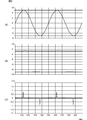
- 2A shows an AC voltage waveform at the connection point A immediately after the sinusoidal AC input voltage is applied to the primary winding, and an applied voltage waveform to the positive ion generator and the negative ion generator
- FIG. 2B is a diagram showing current waveforms flowing in the positive ion generator and the negative ion generator
- FIG. 2C is a diagram showing current waveforms flowing in the positive rectifier circuit and the negative rectifier circuit.
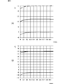
- 3A shows the voltage waveform applied to the positive ion generator and the negative ion generator and the bypass capacitor voltage waveform from the initial state to the steady state
- FIG. 3B shows the positive ion generator and the negative ion generation.
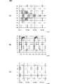
- FIG. 4A shows an AC voltage waveform at a connection point A immediately after applying a sinusoidal AC input voltage to the primary winding in a steady state, and an applied voltage waveform to a positive ion generator and a negative ion generator
- FIG. 4B is a diagram illustrating a current waveform flowing to the positive ion generator and the negative ion generator
- FIG. 4C is a diagram illustrating a current waveform flowing to the positive rectifier circuit and the negative rectifier circuit.
- 5A shows a pulse voltage waveform
- FIG. 5B shows a flyback voltage waveform
- FIG. 5C shows a rectangular wave voltage waveform.
- FIG. 6 is a circuit diagram of another example of the static eliminator.
- 7A and 7B are circuit diagrams of a load device including a power supply device.
- FIG. 8 is a circuit diagram of another example of the power supply apparatus.
- FIG. 9 is a circuit diagram of another example of the power supply apparatus.
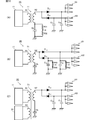
- FIG. 10A, FIG. 10B, and FIG. 10C are circuit diagrams of the static eliminator according to the second embodiment.
- FIG. 11 is a circuit diagram of a static eliminator according to the third embodiment.
- FIG. 12 is a circuit diagram of the static eliminator according to the fourth embodiment.
- FIG. 13 is a circuit diagram of a load device including the power supply device according to the fifth embodiment.
- FIG. 14 is a circuit diagram of a static eliminator including the power supply device according to the sixth embodiment.
- FIG. 15A shows the waveform of the voltage applied to the ion generator
- FIG. 15B shows the waveform of the current flowing to the ion generator.
- FIG. 1 is a circuit diagram of a static eliminator 1 according to the first embodiment.
- the static eliminator 1 includes a power supply device 10, a positive ion generator 101, and a negative ion generator 102.
- the power supply device 10 has a positive output end O1 and a negative output end O2.
- the power supply apparatus 10 outputs a positive high voltage (hereinafter referred to as a positive voltage) from the positive output terminal O1, and outputs a negative high voltage (hereinafter referred to as a negative voltage) from the negative output terminal O2.
- the positive output end O1 is an example of the “positive output end” according to the present invention.
- the negative output terminal O2 is an example of the “negative output terminal” according to the present invention.
- the positive ion generator 101 is connected to the positive output terminal O1.
- the negative ion generator 102 is connected to the negative output terminal O2.
- Each of the positive ion generator 101 and the negative ion generator 102 is a needle-like discharge electrode.
- the power supply device 10 includes a drive circuit 11, a transformer T1, a positive rectifier circuit 12, and a negative rectifier circuit 13.
- the transformer T1 has a primary winding N1 and a secondary winding N2.
- the primary winding N1 is connected to the drive circuit 11.
- the drive circuit 11 supplies an AC voltage to the primary winding N1 of the transformer T1.
- an AC voltage is applied to the primary winding N1 of the transformer T1
- an AC voltage that is twice the turn ratio of the AC voltage applied to the primary winding N1 is generated in the secondary winding N2 of the transformer T1.
- the AC voltage applied to the primary winding N1 is referred to as “input voltage”.
- connection point A a connection point between the second end of the secondary winding N2 and the positive-side rectifier circuit 12 and the negative-side rectifier circuit 13 is referred to as “connection point A”.
- Positive rectifier circuit 12 comprises a diode D 12 and smoothing capacitor C 12.
- the anode of the diode D 12 is connected to the second end of the secondary winding N2, the cathode is connected to the positive output terminal O1.
- Smoothing capacitor C 12 is connected between the cathode and the ground of the diode D 12.
- the positive rectifier circuit 12 is an example embodiment that corresponds to the “first rectifier circuit” according to the present invention.
- Diode D 12 is an example of a "first diode”.
- Smoothing capacitor C 12 is an example of the "first smoothing capacitor” of the present invention. Incidentally, the positive rectifier circuit 12 may not include the smoothing capacitor C 12.
- Negative rectifier circuit 13 comprises a diode D 13 and a smoothing capacitor C 13.
- the cathode of the diode D 13 is connected to the second end of the secondary winding N2, the anode is connected to the negative output terminal O2.
- Smoothing capacitor C 13 is connected between the anode and the ground of the diode D 13.
- the negative rectifier circuit 13 is an example of the “second rectifier circuit” according to the present invention.
- Diode D 13 is an example of a "second diode”.
- Smoothing capacitor C 13 is an example of the "second smoothing capacitor” of the present invention.
- the negative-side rectifying circuit 13 may not include the smoothing capacitor C 13.
- the static eliminator 1 needs to adjust the generation balance of positive and negative ions in order to neutralize the target without biasing the positive / negative potential.
- a current flowing through the positive ion generator 101 hereinafter referred to as positive current
- a current flowing through the negative ion generator 102 hereinafter referred to as negative current.
- the absolute value of The amount of positive ions generated by the positive ion generator 101 is made equal to the amount of negative ions generated by the negative ion generator 102.
- the absolute value of the positive current and the negative current can be made equal by providing the bypass capacitor Cb.
- the reason why the absolute values of the positive current and the negative current are equal when the bypass capacitor Cb is provided will be described.
- FIG. 2A shows an AC voltage waveform at the connection point A immediately after the sinusoidal AC input voltage is applied to the primary winding N1, and applied voltage waveforms to the positive ion generator 101 and the negative ion generator 102.
- FIG. 2B is a diagram illustrating a current waveform flowing through the positive ion generator 101 and the negative ion generator 102
- FIG. 2C is a diagram illustrating a current waveform flowing through the positive rectifier circuit 12 and the negative rectifier circuit 13.
- the solid line waveform indicates the applied voltage to the positive ion generator 101
- the dotted line waveform indicates the applied voltage to the negative ion generator 102.
- FIG. 2B the solid line waveform indicates the current waveform to the positive ion generator 101
- the dotted line waveform indicates the current waveform to the negative ion generator 102.
- FIG. 2C the solid line waveform indicates the inflow current to the positive side rectifier circuit 12, and the dotted line waveform indicates the inflow current to the negative side rectifier circuit 13.
- positive ion is generated in the positive ion generator 101 and positive ions are generated.
- the A positive ion current equal to the amount of generated ionic charge flows through the positive ion generator.
- negative ion corona discharge is generated in the negative ion generator 102 according to the negative voltage applied to the negative ion generator 102 and the ease of ion generation of the negative ion generator 102 to generate negative ions.
- a negative ion current equal to the amount of generated negative ion charge flows through the negative ion generator.
- These ion generator currents are supplied from the secondary winding N2 of the transformer T1 as an inflow / outflow pulse current to the positive rectifier circuit 12 and the negative rectifier circuit 13 as shown in FIG. In this case, the negative pulse current absolute value is larger than the positive pulse current absolute value.
- the positive voltage peak value and the negative voltage peak value are changed, and the positive side rectifier circuit 12 and the negative side rectifier circuit 13 from the connection point A. It can be seen that the sum (difference) of the current values flowing into the current should be zero.
- FIG. 3A shows the voltage waveform applied to the positive ion generator 101 and the negative ion generator 102 and the bypass capacitor voltage waveform from the initial state to the steady state
- FIG. 3B shows the positive ion generator 101 and It is a figure which shows the current waveform which flows into the negative ion generator.
- a solid line waveform is a voltage waveform of the bypass capacitor Cb
- a broken line waveform is a voltage waveform applied to the positive ion generator 101
- a dotted line waveform is a voltage waveform applied to the negative ion generator 102.
- a solid line waveform indicates a current waveform that flows into the positive ion generator 101
- a dotted line waveform indicates a current waveform that flows into the negative ion generator 102.
- the total charge flowing in and out between the connection point A and the positive rectifier circuit 12 and the negative rectifier circuit 13 is supplied by charging / discharging of the bypass capacitor Cb through the secondary winding N2 of the transformer T1.
- FIG. 4A shows the AC voltage waveform at the connection point A immediately after the sinusoidal AC input voltage is applied to the primary winding N1 in the steady state, and the application to the positive ion generator 101 and the negative ion generator 102.
- FIG. 4B shows a voltage waveform
- FIG. 4B shows a current waveform flowing through the positive ion generator 101 and the negative ion generator 102
- FIG. 4C shows a current waveform flowing through the positive rectifier circuit 12 and the negative rectifier circuit 13. It is.
- the voltage waveform at the connection point A is shifted to the positive side, and flows to the positive side rectifier circuit 12 and the negative side rectifier circuit 13 as well as the absolute value of the current flowing through the positive ion generator 101 and the negative ion generator 102. It can be seen that the absolute values of the currents are equal to each other.
- the bypass capacitor Cb By providing the bypass capacitor Cb, the amount of positive and negative ions generated by the positive ion generator 101 and the negative ion generator 102 becomes equal, and the static eliminator 1 having a good balance of positive and negative ion generation is provided. realizable.
- the positive and negative ion generation balance of the static eliminator 1 is maintained, so that the positive / negative ion amount detection or the ionic current detection and the feedback using this are detected. There is no need for control. For this reason, it is not necessary to provide a feedback control circuit, and it is possible to reduce manufacturing costs, reduce costs by reducing parts, and reduce the size.
- the input voltage applied to the primary winding N1 of the transformer T1 is a sine wave AC voltage, but it is not necessarily a sine wave AC voltage.
- a pulse voltage waveform, a flyback voltage waveform, or a rectangular wave voltage waveform as shown in FIGS. 5A, 5B, and 5C may be used.
- 5A shows a pulse voltage waveform
- FIG. 5B shows a flyback voltage waveform
- FIG. 5C shows a rectangular wave voltage waveform.
- FIG. 6 is a circuit diagram of another example of the static eliminator 1A.
- a plurality of positive ion generators 101 are connected to the positive output terminal O1.
- a plurality of negative ion generators 102 are connected to the negative output terminal O2. Even in this configuration, the positive ion current and the negative ion current can be made equal, and the generation balance of positive and negative ions can be adjusted.
- a load other than the positive ion generator and the negative ion generator may be connected to the positive output terminal O1 and the negative output terminal O2 of the power supply device 10.
- FIGS. 7A and 7B are circuit diagrams of a load device including the power supply device 10.
- a load R1 is connected to the positive output end O1
- a load R2 is connected to the negative output end O2.
- a plurality of loads R1 are connected to the positive output terminal O1
- a plurality of loads R2 are connected to the negative output terminal O2. In these configurations, the total amount of current flowing through the loads R1 and R2 can be made equal.
- the bypass capacitor Cb for balancing the generation of positive and negative ions is provided between the secondary winding N2 of the transformer T1 and the ground, but the position where the bypass capacitor Cb is provided. Is not particularly limited.
- the bypass capacitor Cb only needs to be provided on a path from the connection point A through the secondary winding N2 to the ground.
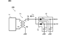
- FIG. 8 is a circuit diagram of another example of the power supply apparatus 10A.
- a bypass capacitor Cb is provided between the secondary winding N2 of the transformer T1 and the connection point A.
- a positive ion generator 101 and a negative ion generator 102 may be connected to the positive output terminal O1 and the negative output terminal O2 of the power supply apparatus 10A, or loads R1 and R2 shown in FIG. May be connected.
- a plurality of positive ion generators 101 and the like may be connected. Even in this configuration, the total amount of current flowing from the positive output terminal O1 and the negative output terminal O2 can be made equal by increasing the charging voltage of the bypass capacitor Cb.
- a static eliminator having a good balance of positive and negative ion generation can be realized.
- FIG. 9 is a circuit diagram of another example of the power supply apparatus 10B.
- the secondary winding of the transformer T1 has a configuration in which a plurality of windings N21, N22, and N23 are connected in series.
- a plurality of bypass capacitors Cb1, Cb2, Cb3, and Cb4 are provided on the secondary side of the transformer T1.
- the bypass capacitor Cb1 is provided between the windings N21 and N22.
- the bypass capacitor Cb2 is provided between the windings N22 and N23.
- the bypass capacitor Cb3 is provided between the winding N23 and the ground.
- the bypass capacitor Cb4 is provided between the winding N21 and the connection point A.
- the withstand voltage required for each winding can be reduced by dividing the secondary winding of the transformer T1 into a plurality.
- the number of secondary windings is three. Further, it is sufficient that at least one bypass capacitor is inserted somewhere between the ground and the connection point A.
- Embodiment 2 are circuit diagrams of the static eliminators 2A, 2B, and 2C according to the second embodiment.
- the static eliminators 2A, 2B, and 2C include a resistance voltage dividing circuit that detects an output voltage.
- a series circuit of voltage dividing resistors R31 and R32 is connected in parallel to the bypass capacitor Cb.
- the voltage of the bypass capacitor Cb can be detected.
- the voltage across the voltage dividing resistor R32 is represented by Vm
- the voltage Vb of the bypass capacitor Cb is Vb ⁇ (R31 + R32) / R32 * Vm.
- the input voltage is V1
- the voltage generated on the secondary side of the transformer T1 is V2
- the number of turns of the primary winding N1 is N1
- the number of turns of the secondary winding N2 is N2
- V2 N2 / N1 * V1.
- the series circuit of the voltage dividing resistors R31 and R32 is an example of the “first resistor voltage dividing circuit” according to the present invention.
- the series circuit of the voltage dividing resistors R41 and R42 is an example of the “second resistor voltage dividing circuit” according to the present invention.
- the series circuit of the voltage dividing resistors R43 and R44 is an example of the “third resistance voltage dividing circuit” according to the present invention.
- the transformer T1 further includes a tertiary winding N3.
- a detection circuit 20 is connected to the tertiary winding N3.
- V3 N3 / N2 * V2
- the voltage V2 of the secondary winding N2 can be detected. From this relationship, it is possible to monitor the output voltage of the static eliminator 2C, detect output abnormality, and the like, as in FIG.
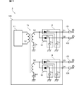
- FIG. 11 is a circuit diagram of the static eliminator 3 according to the third embodiment.
- the static eliminator 3 includes a power supply device 10C.
- the power supply device 10C includes two positive output terminals O1 and O3 and two negative output terminals O2 and O4.
- Positive ion generators 101 and 103 are connected to the positive output terminals O1 and O3, and negative ion generators 102 and 104 are connected to the negative output terminals O2 and O4.
- a plurality of positive ion generators 101 and 103 and negative ion generators 102 and 104 may be connected to the positive output terminals O1 and O3 and the negative output terminals O2 and O4.
- the power supply device 10 ⁇ / b> C includes a drive circuit 11, a transformer T ⁇ b> 2, positive rectifier circuits 12 and 14, and negative rectifier circuits 13 and 15.
- the positive rectifier circuit 14 has the same configuration as that of the positive rectifier circuit 12 and includes a diode D 14 and a smoothing capacitor C 14 .
- Negative rectifier circuit 15 has the same configuration as the negative rectifier circuit 13, a diode D 15 and a smoothing capacitor C 15.
- the transformer T2 includes a primary winding N1 and secondary windings N2 and N4.
- the primary winding N1 is connected to the drive circuit 11.
- the first end of the secondary winding N2 is connected to the ground via the bypass capacitor Cb, and the second end is connected to the positive output terminal O1 and the negative side via the positive rectifier circuit 12 and the negative rectifier circuit 13. It is connected to the output terminal O2.
- the first end of the secondary winding N4 is connected to the ground via the bypass capacitor Cb5, and the second end is connected to the positive output terminal O3 and the negative side via the positive rectifier circuit 14 and the negative rectifier circuit 15. It is connected to the output terminal O4.
- the secondary winding, the positive side rectifier circuits 12 and 14 and the negative side rectifier circuits 13 and 15 connected to the secondary winding are shown in pairs, but any number of pairs may be provided.
- the positive ion generator 101 and the negative ion generator 102, and the positive ion generator 103 and the negative ion generator 104 can be installed at remote locations. It is possible to remove static electricity while maintaining the balance of positive and negative ion generation.
- the total amount of ions generated by the generator 101 and the negative ion generator 102 and the total amount of ions generated by the positive ion generator 103 and the negative ion generator 104 can be made different according to the purpose and application. Become.
- FIG. 12 is a circuit diagram of the static eliminator 4 according to the fourth embodiment.
- the power supply device 10D of the static eliminator 4 has transformers T3, T4, and T5.
- the transformers T3, T4, T5 secondary windings have primary windings N31, N41, N51 and secondary windings N32, N42, N52. Secondary windings N32, N42, and N52 are connected in series.
- the bypass capacitor Cb1 is provided between the secondary windings N32 and N42.
- the bypass capacitor Cb2 is provided between the secondary windings N42 and N52.
- the bypass capacitor Cb3 is provided between the secondary winding N52 and the ground. In this example, there are three sets of transformers.
- FIG. 13 is a circuit diagram of the load device 5 including the power supply device 10E according to the fifth embodiment.
- the power supply device 10E includes a positive rectifier circuit 16 and a negative rectifier circuit 17.
- the second end of the secondary winding N2 is connected to the positive output terminal O1 and the negative output terminal O2 via the positive rectifier circuit 16 and the negative rectifier circuit 17.
- a connection point between the positive rectifier circuit 16 and the negative rectifier circuit 17 and the secondary winding N2 is referred to as a connection point B1.
- the positive side rectifier circuit 16 is a three-stage cockcroft circuit having capacitors C 21 , C 22 , C 23 and diodes D 21 , D 22 , D 23 .
- the positive rectifier circuit 16 is an example embodiment that corresponds to the “first rectifier circuit” according to the present invention.
- the diode D 21 is an example of the “first diode” according to the present invention.
- the negative side rectifier circuit 17 is a three-stage cockcroft circuit having capacitors C 24 , C 25 , C 26 and diodes D 24 , D 25 , D 26 .
- the negative side rectifier circuit 17 is an example embodiment that corresponds to the “second rectifier circuit” according to the present invention.
- the diode D 24 is an example of the “second diode” according to the present invention.
- the diode D 21 rectifies the maximum voltage at node B1. Accordingly, the voltage of the cathode side of the diode D 21 (B2 point) is V2 / 2 + Vb.
- Connection point B4 of the capacitor C 23 and the diode D 23 the voltage maximum voltage at the connection point B3 is rectified, a 3 ⁇ V2 / 2 + Vb.
- the charging voltage of the capacitor C 22 is the maximum voltage at the connection point B1
- Charging voltage of the capacitor C 21 and C 23 is V2.
- the diode D 24 rectifies the minimum voltage at node B1. Accordingly, the voltage of the anode side of the diode D 24 (B5 point) is -V2 / 2 + Vb.
- Connection point B7 between the capacitor C 26 and the diode D 26, the voltage minimum voltage at the connection point B7 is rectified, and -3 ⁇ V2 / 2 + Vb.
- the charging voltage of the capacitor C 25 the absolute value of the minimum voltage at node B1
- the positive and negative currents are equalized by the bypass capacitor Cb and the capacitors C 22 and C 25 .
- the positive side rectifier circuit 16 and the negative side rectifier circuit 17 are three-stage cockcroft circuits, but the positive and negative currents can be made equal even if the number of stages is changed.
- the loads R1 and R2 are, for example, ion generators, but are not limited thereto, and may be other loads.
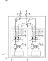
- FIG. 14 is a diagram illustrating the static eliminator 6 including the power supply device 10F according to the present embodiment.
- the power supply device 10F includes two power supply devices 10F1 and 10F2. Since the power supply apparatuses 10F1 and 10F2 have the same configuration as that of the power supply apparatus 10 described in the first embodiment, the same reference numerals are given to the elements constituting the power supply apparatuses 10F1 and 10F2.
- the power supply device 10F1 is an example of the “first positive / negative output circuit” according to the present invention.
- the power supply device 10F2 is an example embodiment that corresponds to the “second positive / negative output circuit” according to the present invention.
- the cathode of the diode D 12 to the power supply 10F1 has, and the anode of the diode D 13 to the power supply 10F2 has been connected through a resistor R51, R52 for short avoided.
- the connection point of the resistors R51 and R52 is connected to the output terminal O5.
- An ion generator 105 is connected to the output end O5.
- the output terminal O5 is an example of the “first positive / negative output terminal” according to the present invention.
- the resistors R51 and R52 are examples of the “first resistor” and the “second resistor” according to the present invention.
- the anode of the diode D 13 to the power supply 10F1 has, and the cathode of the diode D 12 to the power supply 10F2 has been connected through a resistor R53, R54 for short avoided.
- a connection point between the resistors R53 and R54 is connected to the output terminal O6.
- An ion generator 106 is connected to the output end O6.
- the output terminal O6 is an example of the “second positive / negative output terminal” according to the present invention.
- the resistors R53 and R54 are examples of the “third resistor” and the “fourth resistor” according to the present invention.
- the power supply devices 10F1 and 10F2 are operated alternately. Thereby, one ion generator emits positive and negative ions alternately.
- FIG. 15A is a diagram showing a waveform of a voltage applied to the ion generators 105 and 106
- FIG. 15B is a diagram showing a waveform of a current flowing through the ion generators 105 and 106.
- a solid line waveform is a voltage waveform applied to the ion generator 105
- a dotted line waveform is a voltage waveform applied to the ion generator 106.
- the solid line waveform indicates the current waveform to the ion generator 105
- the dotted line waveform indicates the current waveform to the ion generator 106. Note that the dotted line waveform in FIG. 15B is displayed with the sign reversed in accordance with the current direction to the ion generator 105.
- a positive current flows to the ion generator 105 through the resistor R51. Then, positive ions are generated from the ion generator 105. Further, a negative current flows to the ion generator 106 via the resistor R53. Then, negative ions are generated from the ion generator 106. At this time, as described in the first embodiment, positive and negative ions are released in a state where the generation balance is maintained.
- the positive current flows into the negative output terminal O2 of the power supply 10F2 through a resistor R51, R52 is the negative side of the power supply 10 via diode D 13 of the power supply 10F2, diode D 12, a resistor R54, R53 It flows into the output terminal O2. Since this is equivalent to the negative current flowing out from the negative output terminal O2 of the power supply device 10F1, the balance between all positive and negative currents and positive and negative ion currents is maintained.
- a positive current flows from the positive output terminal O1 of the power supply apparatus 10F2 into the power supply apparatus 10F1 via the resistors R54 and R53, and a positive current flows from the negative output terminal O2 of the power supply apparatus 10F2 into the power supply apparatus 10F1 via the resistors R52 and R51.
- Negative currents are equal and all positive and negative currents and positive and negative ion currents are balanced.
- the ion generator 105 generates positive and negative ions alternately.
- the ion generator 106 also generates positive and negative ions alternately. That is, positive and negative ions are alternately emitted from one ion generator.
- positive ions are always released from the positive ion generator, there is a problem that the ion generator is worn by collision of molecules.
- negative ions are always released from the ion generator, there is a problem that siloxane adheres to the ion generator.
- positive or negative ions are always emitted from the ion generator, there is a problem that the positive / negative balance is lost in the vicinity of the ion element.
- the ion balance in the vicinity of the ion element can be maintained.
- the collision time of molecules during generation of positive ions can be shortened, wear of the ion element can be reduced, and similarly, the generation time of negative ions can be shortened, so that the adhesion time of siloxane can be shortened.
- siloxane can be removed by causing molecules to collide with the element when positive ions are generated. As a result, the above-mentioned problems can be solved and the lifetime of the ion generator can be increased.
Landscapes
- Engineering & Computer Science (AREA)
- Power Engineering (AREA)
- Health & Medical Sciences (AREA)
- General Health & Medical Sciences (AREA)
- Toxicology (AREA)
- Elimination Of Static Electricity (AREA)
- Rectifiers (AREA)
Abstract
Description
図1は、実施形態1に係る除電器1の回路図である。
図10(A)、図10(B)及び図10(C)は、実施形態2に係る除電器2A,2B,2Cの回路図である。除電器2A,2B,2Cは、出力電圧を検出する抵抗分圧回路を備えている。
図11は、実施形態3に係る除電器3の回路図である。
図12は、実施形態4に係る除電器4の回路図である。
図13は、実施形態5に係る電源装置10Eを備える負荷装置5の回路図である。
図14は、本実施形態に係る電源装置10Fを備える除電器6を示す図である。
C12,C14…平滑コンデンサ(第1平滑キャパシタ)
C13,C15…平滑コンデンサ(第2平滑キャパシタ)
C21,C22,C23,C24,C25,C26…キャパシタ
Cb,Cb1,Cb2,Cb3,Cb4…バイパスコンデンサ
D12,D14,D21…ダイオード(第1ダイオード)
D13,D15,D24…ダイオード(第2ダイオード)
D22,D23,D25,D26…ダイオード
N1…一次巻線
N2,N4…二次巻線
N21,N22,N23…巻線
N3…三次巻線
N31,N41,N51…一次巻線
N32,N42,N52…二次巻線
O1,O3…正側出力端
O2,O4…負側出力端
O5…出力端(第1正負出力端)
O6…出力端(第2正負出力端)
R1,R2…負荷
R31,R32…分圧抵抗(第1抵抗分圧回路)
R41,R42…分圧抵抗(第2抵抗分圧回路)
R43,R44…分圧抵抗(第3抵抗分圧回路)
R51,R52…抵抗(第1抵抗、第2抵抗)
R53,R54…抵抗(第3抵抗、第4抵抗)
T1,T2,T3,T4,T5…トランス
1,1A,2A,2B,2C,3,4,6…除電器
1B,1C,5…負荷装置
10,10A,10B,10C,10D,10E,10F…電源装置
10F1…電源装置(第1正負出力回路)
10F2…電源装置(第2正負出力回路)
11…駆動回路
12,14,16…正側整流回路
13,15,17…負側整流回路
20…検出回路
101,103…正イオン発生子
102,104…負イオン発生子
105,106…イオン発生子
Claims (11)
- 交流電圧が入力される一次巻線と、第1端がグランドに接続された二次巻線とを有するトランスと、
前記二次巻線の第2端に接続され、アノードが前記第2端に接続され、カソードが正側出力端に接続された第1ダイオードを有する第1整流回路と、
前記二次巻線の第2端に接続され、カソードが前記第2端に接続され、アノードが負側出力端に接続された第2ダイオードを有する第2整流回路と、
前記二次巻線の前記第2端と前記第1整流回路及び前記第2整流回路との接続点から、前記二次巻線を通り、前記グランドまでの経路上のいずれかに設けられたキャパシタと、
を備えた電源装置。 - 前記キャパシタは、
前記二次巻線と、前記グランドとの間に設けられている、
請求項1に記載の電源装置。 - 前記キャパシタは、
前記接続点と前記二次巻線との間に設けられている、
請求項1に記載の電源装置。 - 前記キャパシタに並列接続された第1抵抗分圧回路、
を備えた、請求項1から3のいずれかに記載の電源装置。 - 前記第1整流回路は、
前記第1ダイオードのアノードとグランドとの間に接続された第1平滑キャパシタを有し、
前記第2整流回路は、
前記第2ダイオードのカソードとグランドとの間に接続された第2平滑キャパシタを有している、
請求項1から4のいずれかに記載の電源装置。 - 前記第1平滑キャパシタに並列接続された第2抵抗分圧回路と、
前記第2平滑キャパシタに並列接続された第3抵抗分圧回路と、
を備えた、請求項5に記載の電源装置。 - 前記トランスは三次巻線を有しており、
前記三次巻線に発生する電圧を検出する検出回路をさらに備えている、
請求項1から6のいずれかに記載の電源装置。 - 複数の前記第1整流回路及び前記第2整流回路と、
複数の前記正側出力端及び前記負側出力端と、
を備え、
前記トランスは複数の二次巻線を有し、
前記複数の二次巻線それぞれの第2端は、前記第1整流回路及び前記第2整流回路を介して、前記正側出力端及び前記負側出力端に接続されている、
請求項1から7のいずれかに記載の電源装置。 - 第1正負出力回路と
第2正負出力回路と、
を備え、
前記第1正負出力回路及び前記第2正負出力回路それぞれは、
正側出力端及び負側出力端と、
交流電圧が入力される一次巻線と、第1端がグランドに接続された二次巻線とを有するトランスと、
前記二次巻線の第2端に接続され、アノードが前記第2端に接続され、カソードが前記正側出力端に接続された第1ダイオードを有する第1整流回路と、
前記二次巻線の第2端に接続され、カソードが前記第2端に接続され、アノードが前記負側出力端に接続された第2ダイオードを有する第2整流回路と、
前記二次巻線の前記第2端と前記第1整流回路及び前記第2整流回路との接続点から、前記二次巻線を通り、前記グランドまでの経路上のいずれかに設けられたキャパシタと、
を有し、
前記第1正負出力回路が有する前記正側出力端と、前記第2正負出力回路が有する前記負側出力端とは、第1抵抗及び第2抵抗を介して接続され、
前記第1正負出力回路が有する前記負側出力端と、前記第2正負出力回路が有する前記正側出力端とは、第3抵抗及び第4抵抗を介して接続され、
前記第1抵抗と前記第2抵抗との接続点は、第1正負出力端に接続され、
前記第3抵抗と前記第4抵抗との接続点は、第2正負出力端に接続されている、
電源装置。 - 請求項1から8のいずれかに記載の電源装置と、
前記正側出力端に接続された正イオン発生子と、
前記負側出力端に接続された負イオン発生子と、
を備えた除電器。 - 請求項9に記載の電源装置と、
前記第1正負出力端及び前記第2正負出力端それぞれに接続されたイオン発生子、
を備えた除電器。
Priority Applications (4)
| Application Number | Priority Date | Filing Date | Title |
|---|---|---|---|
| JP2017520285A JP6477871B2 (ja) | 2015-05-26 | 2016-04-07 | 電源装置及び除電器 |
| CN201680029829.1A CN107615887A (zh) | 2015-05-26 | 2016-04-07 | 电源装置以及除电器 |
| KR1020177031359A KR101982497B1 (ko) | 2015-05-26 | 2016-04-07 | 전원 장치 |
| US15/810,200 US10148193B2 (en) | 2015-05-26 | 2017-11-13 | Power supply unit and static eliminator |
Applications Claiming Priority (2)
| Application Number | Priority Date | Filing Date | Title |
|---|---|---|---|
| JP2015106263 | 2015-05-26 | ||
| JP2015-106263 | 2015-05-26 |
Related Child Applications (1)
| Application Number | Title | Priority Date | Filing Date |
|---|---|---|---|
| US15/810,200 Continuation US10148193B2 (en) | 2015-05-26 | 2017-11-13 | Power supply unit and static eliminator |
Publications (1)
| Publication Number | Publication Date |
|---|---|
| WO2016189980A1 true WO2016189980A1 (ja) | 2016-12-01 |
Family
ID=57393178
Family Applications (1)
| Application Number | Title | Priority Date | Filing Date |
|---|---|---|---|
| PCT/JP2016/061346 Ceased WO2016189980A1 (ja) | 2015-05-26 | 2016-04-07 | 電源装置及び除電器 |
Country Status (5)
| Country | Link |
|---|---|
| US (1) | US10148193B2 (ja) |
| JP (1) | JP6477871B2 (ja) |
| KR (1) | KR101982497B1 (ja) |
| CN (1) | CN107615887A (ja) |
| WO (1) | WO2016189980A1 (ja) |
Cited By (4)
| Publication number | Priority date | Publication date | Assignee | Title |
|---|---|---|---|---|
| JPWO2018030072A1 (ja) * | 2016-08-09 | 2019-06-06 | 株式会社村田製作所 | 電源装置及び除電器 |
| JP2021044144A (ja) * | 2019-09-11 | 2021-03-18 | シャープ株式会社 | イオン発生装置、及びイオン発生システム |
| JP2021090301A (ja) * | 2019-12-05 | 2021-06-10 | 三菱パワー株式会社 | 電源回路及び入出力モジュール |
| US20240079857A1 (en) * | 2022-09-07 | 2024-03-07 | Keyence Corporation | Static eliminator and ion balance control method |
Families Citing this family (4)
| Publication number | Priority date | Publication date | Assignee | Title |
|---|---|---|---|---|
| CN108493776B (zh) * | 2018-05-22 | 2024-07-23 | 芜湖美智空调设备有限公司 | 正负离子控制电路及其控制方法 |
| CN110446322B (zh) * | 2019-07-31 | 2023-11-28 | 深圳市凯仕德科技有限公司 | 离子风机的放电方法、离子风机的放电装置以及离子风机 |
| TWI746151B (zh) * | 2020-09-07 | 2021-11-11 | 國立臺北科技大學 | 可調頻離子機控制裝置 |
| CN115765499A (zh) * | 2022-11-23 | 2023-03-07 | 珠海格力电器股份有限公司 | 负离子发生装置和电气设备 |
Citations (6)
| Publication number | Priority date | Publication date | Assignee | Title |
|---|---|---|---|---|
| JPH04368466A (ja) * | 1991-06-14 | 1992-12-21 | Sony Corp | スイッチング電源装置 |
| JPH10191549A (ja) * | 1996-12-25 | 1998-07-21 | Yokogawa Denshi Kiki Kk | 除電器の安全装置 |
| JP2000058290A (ja) * | 1998-06-04 | 2000-02-25 | Keyence Corp | 除電装置 |
| JP2007027015A (ja) * | 2005-07-21 | 2007-02-01 | Sharp Corp | イオン発生装置及び空気調節装置 |
| JP2008016274A (ja) * | 2006-07-05 | 2008-01-24 | Sunx Ltd | 除電装置 |
| JP2010218750A (ja) * | 2009-03-13 | 2010-09-30 | Omron Corp | 除電装置 |
Family Cites Families (20)
| Publication number | Priority date | Publication date | Assignee | Title |
|---|---|---|---|---|
| US3723850A (en) * | 1971-07-23 | 1973-03-27 | Ferromagnetics Inc | High voltage power supply for copying apparatus or the like |
| US3819980A (en) * | 1972-03-16 | 1974-06-25 | Gen Motors Corp | Emergency lighting system |
| US4158881A (en) * | 1978-06-12 | 1979-06-19 | Litton Systems, Inc. | DC to DC converter |
| US4673888A (en) * | 1986-09-02 | 1987-06-16 | Electro-Voice, Inc. | Power control system |
| JPS6420085U (ja) * | 1987-07-22 | 1989-01-31 | ||
| JPH074797Y2 (ja) * | 1991-09-26 | 1995-02-01 | 春日電機株式会社 | 直流除電器 |
| CN2170619Y (zh) * | 1993-01-19 | 1994-06-29 | 徐国忠 | 分流式直流静电消除器 |
| JP4367580B2 (ja) | 1997-04-14 | 2009-11-18 | 株式会社キーエンス | 除電装置 |
| JP2001157142A (ja) * | 1999-11-26 | 2001-06-08 | Sony Corp | 電気機器 |
| JP2001314079A (ja) * | 2000-04-28 | 2001-11-09 | Sony Corp | スイッチング電源回路 |
| KR20030081476A (ko) * | 2001-03-05 | 2003-10-17 | 소니 가부시끼 가이샤 | 스위칭 소자에 의해 구동주파수를 가변제어한 스위칭전원회로 |
| JP4954633B2 (ja) | 2005-08-24 | 2012-06-20 | 株式会社山梨技術工房 | 高電圧発生回路およびイオナイザー |
| JP4818093B2 (ja) * | 2006-12-19 | 2011-11-16 | ミドリ安全株式会社 | 除電装置 |
| JP5217535B2 (ja) * | 2008-03-17 | 2013-06-19 | サンケン電気株式会社 | Dc−dcコンバータ |
| JP5344562B2 (ja) * | 2008-12-01 | 2013-11-20 | ヒューグルエレクトロニクス株式会社 | イオナイザおよびイオナイザシステム |
| US8085561B2 (en) * | 2009-03-03 | 2011-12-27 | Gary Hanington | Power supply with integrated concentric high voltage multiplier |
| JP5351598B2 (ja) | 2009-04-24 | 2013-11-27 | ミドリ安全株式会社 | 除電装置 |
| JP5510032B2 (ja) * | 2009-05-14 | 2014-06-04 | 日産自動車株式会社 | 非接触給電装置 |
| JP5508302B2 (ja) * | 2011-01-21 | 2014-05-28 | 株式会社キーエンス | 除電器 |
| JP5828273B2 (ja) * | 2011-12-01 | 2015-12-02 | 富士電機株式会社 | スイッチング電源装置 |
-
2016
- 2016-04-07 KR KR1020177031359A patent/KR101982497B1/ko active Active
- 2016-04-07 CN CN201680029829.1A patent/CN107615887A/zh active Pending
- 2016-04-07 JP JP2017520285A patent/JP6477871B2/ja active Active
- 2016-04-07 WO PCT/JP2016/061346 patent/WO2016189980A1/ja not_active Ceased
-
2017
- 2017-11-13 US US15/810,200 patent/US10148193B2/en active Active
Patent Citations (6)
| Publication number | Priority date | Publication date | Assignee | Title |
|---|---|---|---|---|
| JPH04368466A (ja) * | 1991-06-14 | 1992-12-21 | Sony Corp | スイッチング電源装置 |
| JPH10191549A (ja) * | 1996-12-25 | 1998-07-21 | Yokogawa Denshi Kiki Kk | 除電器の安全装置 |
| JP2000058290A (ja) * | 1998-06-04 | 2000-02-25 | Keyence Corp | 除電装置 |
| JP2007027015A (ja) * | 2005-07-21 | 2007-02-01 | Sharp Corp | イオン発生装置及び空気調節装置 |
| JP2008016274A (ja) * | 2006-07-05 | 2008-01-24 | Sunx Ltd | 除電装置 |
| JP2010218750A (ja) * | 2009-03-13 | 2010-09-30 | Omron Corp | 除電装置 |
Cited By (8)
| Publication number | Priority date | Publication date | Assignee | Title |
|---|---|---|---|---|
| JPWO2018030072A1 (ja) * | 2016-08-09 | 2019-06-06 | 株式会社村田製作所 | 電源装置及び除電器 |
| JP2021044144A (ja) * | 2019-09-11 | 2021-03-18 | シャープ株式会社 | イオン発生装置、及びイオン発生システム |
| JP7299806B2 (ja) | 2019-09-11 | 2023-06-28 | シャープ株式会社 | イオン発生装置、及びイオン発生システム |
| JP2021090301A (ja) * | 2019-12-05 | 2021-06-10 | 三菱パワー株式会社 | 電源回路及び入出力モジュール |
| WO2021111764A1 (ja) * | 2019-12-05 | 2021-06-10 | 三菱パワー株式会社 | 電源回路及び入出力モジュール |
| US11764700B2 (en) | 2019-12-05 | 2023-09-19 | Mitsubishi Heavy Industries, Ltd. | Power supply circuit and input/output module |
| US20240079857A1 (en) * | 2022-09-07 | 2024-03-07 | Keyence Corporation | Static eliminator and ion balance control method |
| US12374869B2 (en) * | 2022-09-07 | 2025-07-29 | Keyence Corporation | Static eliminator and ion balance control method |
Also Published As
| Publication number | Publication date |
|---|---|
| US10148193B2 (en) | 2018-12-04 |
| KR101982497B1 (ko) | 2019-05-27 |
| US20180069484A1 (en) | 2018-03-08 |
| CN107615887A (zh) | 2018-01-19 |
| JP6477871B2 (ja) | 2019-03-06 |
| KR20170132287A (ko) | 2017-12-01 |
| JPWO2016189980A1 (ja) | 2018-02-15 |
Similar Documents
| Publication | Publication Date | Title |
|---|---|---|
| JP6477871B2 (ja) | 電源装置及び除電器 | |
| KR101158455B1 (ko) | 무정전 전원 장치 | |
| US9030856B2 (en) | High voltage inverter device and electrical leakage detector thereof | |
| KR20120085204A (ko) | 제전기 | |
| US9584032B2 (en) | Multi-output DC-to-DC power converter | |
| JPWO2017145380A1 (ja) | 直流高圧電源装置 | |
| EP2624423A2 (en) | Buck DC-TO-DC converter having a novel output protection mechanism | |
| KR101937755B1 (ko) | 이오나이저 | |
| JP6727436B2 (ja) | パルス電源装置 | |
| US9812847B2 (en) | Ionizer | |
| JP5460546B2 (ja) | 除電装置 | |
| US9600012B2 (en) | Internal power supply of a device | |
| JP6536750B2 (ja) | 電源装置及び除電器 | |
| US9530634B2 (en) | Device for supplying voltage to the cathode of a mass spectrometer | |
| KR101727330B1 (ko) | 제전 장치 | |
| JP6371226B2 (ja) | 逆電流保護付きスイッチング電源装置 | |
| JP2011004503A (ja) | 電源装置及び補正回路 | |
| CN109075716B (zh) | 具有电隔离的钟控电源单元 | |
| EP2975727A1 (en) | Three-wire UPS system with artificial neutral | |
| JP6635513B2 (ja) | スイッチング電源装置 | |
| JP4638309B2 (ja) | 交流安定化電源装置 | |
| US9966858B2 (en) | DC-DC converting apparatus for obtaining a constant output voltage | |
| JP2007288973A (ja) | 正負切り換え電源装置 | |
| US20120152301A1 (en) | Center-tapped solar array and power distribution system for same | |
| JP2008035647A (ja) | 直流電源装置 |
Legal Events
| Date | Code | Title | Description |
|---|---|---|---|
| 121 | Ep: the epo has been informed by wipo that ep was designated in this application |
Ref document number: 16799688 Country of ref document: EP Kind code of ref document: A1 |
|
| ENP | Entry into the national phase |
Ref document number: 2017520285 Country of ref document: JP Kind code of ref document: A |
|
| ENP | Entry into the national phase |
Ref document number: 20177031359 Country of ref document: KR Kind code of ref document: A |
|
| NENP | Non-entry into the national phase |
Ref country code: DE |
|
| 122 | Ep: pct application non-entry in european phase |
Ref document number: 16799688 Country of ref document: EP Kind code of ref document: A1 |