WO2016186099A1 - 導電性粘着材及び導電性基材付き導電性粘着材 - Google Patents
導電性粘着材及び導電性基材付き導電性粘着材 Download PDFInfo
- Publication number
- WO2016186099A1 WO2016186099A1 PCT/JP2016/064559 JP2016064559W WO2016186099A1 WO 2016186099 A1 WO2016186099 A1 WO 2016186099A1 JP 2016064559 W JP2016064559 W JP 2016064559W WO 2016186099 A1 WO2016186099 A1 WO 2016186099A1
- Authority
- WO
- WIPO (PCT)
- Prior art keywords
- conductive
- particles
- adhesive material
- less
- conductive adhesive
- Prior art date
- Legal status (The legal status is an assumption and is not a legal conclusion. Google has not performed a legal analysis and makes no representation as to the accuracy of the status listed.)
- Ceased
Links
Images


Classifications
-
- C—CHEMISTRY; METALLURGY
- C09—DYES; PAINTS; POLISHES; NATURAL RESINS; ADHESIVES; COMPOSITIONS NOT OTHERWISE PROVIDED FOR; APPLICATIONS OF MATERIALS NOT OTHERWISE PROVIDED FOR
- C09J—ADHESIVES; NON-MECHANICAL ASPECTS OF ADHESIVE PROCESSES IN GENERAL; ADHESIVE PROCESSES NOT PROVIDED FOR ELSEWHERE; USE OF MATERIALS AS ADHESIVES
- C09J11/00—Features of adhesives not provided for in group C09J9/00, e.g. additives
- C09J11/02—Non-macromolecular additives
- C09J11/04—Non-macromolecular additives inorganic
-
- C—CHEMISTRY; METALLURGY
- C09—DYES; PAINTS; POLISHES; NATURAL RESINS; ADHESIVES; COMPOSITIONS NOT OTHERWISE PROVIDED FOR; APPLICATIONS OF MATERIALS NOT OTHERWISE PROVIDED FOR
- C09J—ADHESIVES; NON-MECHANICAL ASPECTS OF ADHESIVE PROCESSES IN GENERAL; ADHESIVE PROCESSES NOT PROVIDED FOR ELSEWHERE; USE OF MATERIALS AS ADHESIVES
- C09J201/00—Adhesives based on unspecified macromolecular compounds
-
- C—CHEMISTRY; METALLURGY
- C09—DYES; PAINTS; POLISHES; NATURAL RESINS; ADHESIVES; COMPOSITIONS NOT OTHERWISE PROVIDED FOR; APPLICATIONS OF MATERIALS NOT OTHERWISE PROVIDED FOR
- C09J—ADHESIVES; NON-MECHANICAL ASPECTS OF ADHESIVE PROCESSES IN GENERAL; ADHESIVE PROCESSES NOT PROVIDED FOR ELSEWHERE; USE OF MATERIALS AS ADHESIVES
- C09J7/00—Adhesives in the form of films or foils
- C09J7/20—Adhesives in the form of films or foils characterised by their carriers
-
- C—CHEMISTRY; METALLURGY
- C09—DYES; PAINTS; POLISHES; NATURAL RESINS; ADHESIVES; COMPOSITIONS NOT OTHERWISE PROVIDED FOR; APPLICATIONS OF MATERIALS NOT OTHERWISE PROVIDED FOR
- C09J—ADHESIVES; NON-MECHANICAL ASPECTS OF ADHESIVE PROCESSES IN GENERAL; ADHESIVE PROCESSES NOT PROVIDED FOR ELSEWHERE; USE OF MATERIALS AS ADHESIVES
- C09J7/00—Adhesives in the form of films or foils
- C09J7/20—Adhesives in the form of films or foils characterised by their carriers
- C09J7/28—Metal sheet
-
- C—CHEMISTRY; METALLURGY
- C09—DYES; PAINTS; POLISHES; NATURAL RESINS; ADHESIVES; COMPOSITIONS NOT OTHERWISE PROVIDED FOR; APPLICATIONS OF MATERIALS NOT OTHERWISE PROVIDED FOR
- C09J—ADHESIVES; NON-MECHANICAL ASPECTS OF ADHESIVE PROCESSES IN GENERAL; ADHESIVE PROCESSES NOT PROVIDED FOR ELSEWHERE; USE OF MATERIALS AS ADHESIVES
- C09J9/00—Adhesives characterised by their physical nature or the effects produced, e.g. glue sticks
- C09J9/02—Electrically-conducting adhesives
-
- H—ELECTRICITY
- H05—ELECTRIC TECHNIQUES NOT OTHERWISE PROVIDED FOR
- H05K—PRINTED CIRCUITS; CASINGS OR CONSTRUCTIONAL DETAILS OF ELECTRIC APPARATUS; MANUFACTURE OF ASSEMBLAGES OF ELECTRICAL COMPONENTS
- H05K9/00—Screening of apparatus or components against electric or magnetic fields
Definitions
- the present invention relates to a conductive adhesive material, and more particularly to a conductive adhesive material suitably used for shielding electromagnetic waves. Moreover, this invention relates to the conductive adhesive material with a conductive base material using the said conductive adhesive material.
- an electromagnetic shielding material has been used to protect circuits and electronic component elements in electrical or electronic equipment.
- an adhesive sheet containing metal particles is used as an electromagnetic shielding material. Moreover, this adhesive sheet may be used by laminating on a conductive substrate.
- Patent Document 1 discloses that a conductive resin composition containing conductive particles and a resin is used as an electromagnetic shielding material.
- the conductive particles include a nucleus containing a conductive substance and a coating layer covering the nucleus.
- the coating layer is made of a conductive material different from the core, and at least a part of it forms the outermost layer.
- the conventional electromagnetic shielding material such as Patent Document 1 may not fully exhibit the electromagnetic shielding function.
- the surface of the adherend to which the electromagnetic wave shielding material is applied has irregularities, there is a problem that the electromagnetic wave shielding function tends to be lowered.
- the conductive particle includes a plurality of metal particles, a plurality of conductive particles, and an adhesive component, the conductive particles excluding the metal particles, and the surface of the substrate particles.
- a conductive pressure-sensitive adhesive material wherein the conductive particle has a plurality of protrusions on an outer surface of the conductive portion.
- the content of the conductive particles is 1% by weight to 30% by weight in 100% by weight of the conductive adhesive material.
- the conductive particles have a particle diameter of 3 ⁇ m or more and 40 ⁇ m or less.
- the volume resistivity of the conductive particles is 0.001 ⁇ ⁇ cm or less.
- the ratio of the particle size of the conductive particles to the particle size of the metal particles is 0.7 or more and 5000 or less.
- the average height of the protrusions is 30 nm or more and 1000 nm or less.
- the surface area of the portion where the protrusion is present is 0.1% or more out of 100% of the total surface area of the outer surface of the conductive part.
- the conductive particles include a plurality of core substances that protrude the outer surface of the conductive part.
- the material of the core substance has a Mohs hardness of 5 or more.
- the thickness of the conductive adhesive material is 5 ⁇ m or more and 40 ⁇ m or less.
- a conductive group having the above-described conductive adhesive material and a conductive base material, wherein the conductive adhesive material is disposed on the surface of the conductive base material.
- a conductive adhesive with a material is provided.
- the conductive substrate is a copper foil.
- the conductive adhesive material according to the present invention includes a plurality of metal particles, a plurality of conductive particles, and an adhesive component, and the conductive particles include base particles excluding the metal particles, and the surfaces of the base particles.
- An electroconductive particle having a conductive portion disposed thereon, and the conductive particle has a plurality of protrusions on the outer surface of the conductive portion. Function can be enhanced sufficiently.
- FIG. 1 is a cross-sectional view showing a conductive adhesive with a conductive substrate according to an embodiment of the present invention.
- FIG. 2 is a cross-sectional view showing conductive particles used in the conductive adhesive material with a conductive substrate according to an embodiment of the present invention.
- FIG. 3 is a cross-sectional view showing a first modification of the conductive particles.
- FIG. 4 is a cross-sectional view showing a second modification of the conductive particles.
- FIG. 5 is a cross-sectional view showing a third modification of the conductive particles.
- FIG. 6 is a diagram for explaining a connection resistance evaluation method.
- the conductive adhesive material according to the present invention is particularly preferably used for shielding electromagnetic waves.
- the conductive adhesive material according to the present invention is particularly preferably used as an electromagnetic shielding material.
- the conductive adhesive material according to the present invention has an electromagnetic wave shielding function.
- the electroconductive adhesive material which concerns on this invention may be arrange
- the conductive adhesive material according to the present invention is an adhesive layer.
- the conductive adhesive material according to the present invention is suitably used to obtain a conductive adhesive material with a conductive substrate comprising the above conductive adhesive material (adhesive layer) and a conductive substrate.
- the conductive adhesive material (adhesive layer) may be disposed on the surface of the conductive substrate.
- the conductive adhesive material according to the present invention includes a plurality of metal particles, a plurality of conductive particles, and an adhesive component.
- the conductive particles are conductive particles including base particles excluding metal particles and conductive portions disposed on the surface of the base particles.
- the conductive particles have a plurality of protrusions on the outer surface of the conductive part.
- the electromagnetic wave shielding function can be sufficiently enhanced even if the surface of the adherend has irregularities.
- the conductive particles comprising, as the conductive particles, base particles excluding the metal particles, and conductive portions arranged on the surface of the base particles.
- the combination of the configuration in which the conductive particles have protrusions on the outer surface of the conductive portion greatly contributes to the improvement of the electromagnetic wave shielding function when the electromagnetic wave shielding material is applied to the uneven surface.
- the conductive particles have protrusions on the outer surface of the conductive portion, the conductive adhesive material can be satisfactorily followed with respect to the uneven surface. As a result, the electromagnetic wave shielding function is enhanced.
- the conductive adhesive material according to the present invention has good applicability when the conductive adhesive material is formed.
- the dispersibility of the conductive particles is good, the distribution of the adhesive component in the application region becomes extremely uniform, and the variation in the adhesive strength can be reduced.
- the conductive adhesive material according to the present invention has the above-described configuration, the conduction path is not easily cut off due to the displacement of the adhesive portion due to heat, impact, etc., so that the durability and heat resistance of the electromagnetic wave shield are sufficiently obtained. Can be increased.
- the electroconductive adhesive material which concerns on this invention has said structure, when arrange
- the content of the conductive particles is preferably 1% by weight or more and 30% by weight or less.
- FIG. 1 is a cross-sectional view of a conductive adhesive material with a conductive base material according to an embodiment of the present invention.
- the conductive adhesive material with a conductive substrate includes a conductive adhesive material.
- the conductive adhesive material 52 has a conductive adhesive material 52 and a conductive base material 53.
- the conductive adhesive material 52 is disposed on the surface of the conductive substrate 53.
- the conductive adhesive material 52 includes a plurality of metal particles 56, a plurality of conductive particles 1, and an adhesive component 57.
- the conductive base material the conductive adhesive material, the metal particles contained in the conductive adhesive material, the conductive particles contained in the conductive adhesive material, and the adhesive component contained in the conductive adhesive material will be described in more detail.
- the conductive pressure-sensitive adhesive material of the present invention can be formed into a conductive pressure-sensitive adhesive sheet, a conductive pressure-sensitive adhesive tape, or the like by arranging it on a conductive base material as described above.
- a conductive base material metal base materials, such as metal foil, a metal mesh, and a metal plate, are mentioned.
- the material for the conductive substrate include copper and aluminum.
- the metal foil include copper foil and aluminum foil.
- the conductive substrate is preferably a metal substrate, more preferably a metal foil, a metal mesh, or a metal plate, and even more preferably a metal foil.
- the material of the conductive substrate is preferably copper or aluminum, and more preferably copper.
- the conductive substrate is more preferably a copper foil or an aluminum foil, and even more preferably a copper foil.
- the thickness of the conductive substrate is preferably 5 ⁇ m or more, more preferably 10 ⁇ m or more, preferably 40 ⁇ m or less, more preferably 30 ⁇ m or less, and even more preferably 20 ⁇ m or less. is there.
- the thickness of the conductive adhesive is preferably 5 ⁇ m or more, more preferably 10 ⁇ m or more, preferably 40 ⁇ m or less, more preferably 30 ⁇ m or less, and even more preferably 20 ⁇ m or less. is there.
- the conductive adhesive material according to the present invention the content of metal particles can be relatively reduced by using conductive particles, so that aggregation of metal particles can be suppressed. As a result, the thickness of the conductive adhesive material can be 20 ⁇ m or less, and the adhesive tape can be made thinner.
- an adhesive sheet and an adhesive film are contained in an adhesive tape.
- the ratio of the thickness of the conductive adhesive material to the particle diameter of the conductive particles is preferably 0.125 or more.
- it is 0.3 or more, More preferably, it is 0.5 or more,
- it is 20 or less, More preferably, it is 10 or less, More preferably, it is 5 or less, More preferably, it is 1.8 or less.
- the ratio is not less than the above lower limit and not more than the above upper limit, the electromagnetic wave shielding function is effectively enhanced.
- the said metal particle is a metal particle in which both the center part and the surface part are formed with the metal. This metal particle does not have base material particles other than the metal particle in the center.
- the metal species in the central part and the surface part and the proportion thereof may be the same or different.
- the metal that is the material of the metal particles is not particularly limited.
- the metal particle material include gold, silver, copper, palladium, ruthenium, rhodium, iridium, lithium, platinum, zinc, iron, tin, lead, aluminum, cobalt, indium, nickel, chromium, titanium, and antimony. Bismuth, thallium, germanium, cadmium, silicon, tungsten, molybdenum and alloys thereof.
- the metal include tin-doped indium oxide (ITO) and solder.
- the electromagnetic wave shielding function can be effectively enhanced, an alloy containing tin, nickel, palladium, silver, copper or gold is preferable, nickel, palladium, copper or silver is more preferable, and nickel, palladium or copper is further preferable.
- the conductive portion contains nickel and phosphorus or boron.
- the metal particle material may be an alloy containing phosphorus, boron, or the like. In the metal particles, nickel and tungsten or molybdenum may be alloyed.
- the content of nickel, palladium, copper or silver in 100% by weight of the metal particles is preferably 10% by weight or more, more preferably 25% by weight or more, still more preferably 40% by weight or more, preferably 100% by weight ( Total amount) or less.
- the nickel content in the metal particles is preferably not less than the above lower limit and not more than the above upper limit.
- the metal particles preferably contain nickel as a main metal. It is preferable that the content of nickel is 50% by weight or more in the total 100% by weight of the metal particles. In 100% by weight of the metal particles, the nickel content is preferably 65% by weight or more, more preferably 80% by weight or more, and still more preferably 90% by weight or more. When the nickel content is not less than the above lower limit, the electromagnetic shielding function is effectively enhanced.
- the content of the metal particles is preferably 1% by weight or more, more preferably 5% by weight or more, preferably 25% by weight or less, more preferably 15% by weight or less.
- the electromagnetic shielding function is effectively enhanced.
- the electromagnetic wave shielding function can be sufficiently enhanced even if the content of the metal particles is small.
- FIG. 2 is a cross-sectional view showing conductive particles used in the conductive adhesive material in the conductive adhesive material with a conductive substrate according to an embodiment of the present invention.
- the conductive particle 1 shown in FIG. 1 includes a base particle 2, a conductive portion 3, and a core substance 4.
- the conductive part 3 is disposed on the surface of the base particle 2.
- the conductive particle 1 is a coated particle in which the surface of the base particle 2 is coated with the conductive portion 3.
- the conductive part 3 is a continuous film.
- the conductive particles 1 have a plurality of protrusions on the conductive surface.
- the conductive portion 3 has a plurality of protrusions 3a on the outer surface.
- a plurality of core substances 4 are arranged on the surface of the base particle 2.
- the plurality of core materials 4 are disposed inside the conductive portion 3 and are embedded in the conductive portion 3.
- the conductive portion 3 covers a plurality of core materials 4.
- the outer surface of the conductive portion 3 is raised by the plurality of core materials 4 and the protrusions 3a are formed.
- the conductive particle 1 includes a core material 4 that is raised on the outer surface of the conductive portion 3 so as to form a protrusion 3a.
- FIG. 3 is a cross-sectional view showing a first modification of the conductive particles.
- 3 includes a base particle 2 and a conductive portion 3A.
- the conductive part 3 ⁇ / b> A is disposed on the surface of the base particle 2.
- the conductive particles 1A have a plurality of protrusions on the conductive surface.
- the conductive portion 3A has a plurality of protrusions 3Aa on the outer surface.
- the conductive particle 1A does not include a core substance.
- the conductive portion 3A has a first portion and a second portion that is thicker than the first portion.
- a portion excluding the plurality of protrusions 3Aa is the first portion of the conductive portion 3A.
- the plurality of protrusions 3Aa are the second portions where the thickness of the conductive portion 3A is thick.
- the core substance is not necessarily used to form the protrusions.
- FIG. 4 is a cross-sectional view showing a second modification of the conductive particles.
- the conductive particle 1B shown in FIG. 1 includes a base particle 2, a conductive portion 3B, and a core substance 4.
- the conductive particle 1B has a plurality of protrusions on the conductive surface.
- the conductive portion 3B has a plurality of protrusions 3Ba on the outer surface.
- the position of the core substance and the conductive part are different.
- the conductive portion 3 having a single layer structure is formed, whereas in the conductive particle 1B, a multi-layer (two layers) conductive portion 3B is formed.
- the conductive part 3B has a first conductive part 3BA and a second conductive part 3BB.
- the first and second conductive portions 3BA and 3BB are disposed on the surface of the base particle 2.
- the first conductive portion 3BA is disposed between the base particle 2 and the second conductive portion 3BB. Accordingly, the first conductive portion 3BA is disposed on the surface of the base particle 2, and the second conductive portion 3BB is disposed on the surface of the first conductive portion 3BA.
- the outer shape of the first conductive portion 3BA is spherical.
- the first conductive portion 3BA has no protrusion on the outer surface.
- the second conductive portion 3BB has a plurality of protrusions 3BBa on the outer surface.
- a plurality of core materials 4 are arranged on the surface of the first conductive portion 3BA.
- the plurality of core materials 4 are arranged inside the second conductive portion 3BB and are embedded in the second conductive portion 3BB.
- the second conductive portion 3BB covers a plurality of core substances 4.
- the outer surface of the conductive portion 3 ⁇ / b> B is raised by the plurality of core materials 4, and the protrusion 3 ⁇ / b> Ba is formed.
- the outer surface of the second conductive portion 3BB is raised by the plurality of core materials 4 to form protrusions 3BBa.
- the conductive portion may not be a single layer but may be a multilayer.
- FIG. 5 is a cross-sectional view showing a third modification of the conductive particles.
- a conductive particle 1 ⁇ / b> C shown in FIG. 5 includes a base particle 2, a conductive part 3 ⁇ / b> C, and a core substance 4.
- the conductive particles 1C have a plurality of protrusions on the conductive surface.
- the conductive portion 3C has a plurality of protrusions 3Ca on the outer surface.
- the conductive particles 1B and the conductive particles 1C differ only in the conductive portion due to the difference in the position of the core substance.
- the conductive part 3C has a first conductive part 3CA and a second conductive part 3CB.
- the first and second conductive portions 3CA and 3CB are disposed on the surface of the base particle 2.
- a first conductive portion 3CA is disposed between the base particle 2 and the second conductive portion 3CB. Therefore, the first conductive portion 3CA is disposed on the surface of the base particle 2, and the second conductive portion 3CB is disposed on the surface of the first conductive portion 3CA.
- the first conductive portion 3CA has a plurality of protrusions 3CAa on the outer surface.
- the second conductive portion 3CB has a plurality of protrusions 3CBa on the outer surface.
- a plurality of core substances 4 are arranged on the surface of the base particle 2.
- the plurality of core materials 4 are disposed inside the conductive portion 3C and are embedded in the conductive portion 3C.
- the plurality of core materials 4 are arranged inside the first conductive portion 3CA and are embedded in the first conductive portion 3CA.
- the conductive portion 3 ⁇ / b> C covers a plurality of core materials 4.
- the outer surface of the conductive portion 3 ⁇ / b> C is raised by the plurality of core materials 4, and the protrusion 3 ⁇ / b> Ca is formed.
- the first conductive portion 3CA covers a plurality of core substances 4.
- the outer surface of the first conductive portion 3CA is raised by the plurality of core materials 4 to form protrusions 3CAa, and further, protrusions 3CBa are formed.
- the volume resistivity of the conductive particles is preferably 0.1 ⁇ ⁇ cm or less, more preferably 0.02 ⁇ ⁇ cm or less, and further preferably 0.001 ⁇ ⁇ cm or less.
- the volume resistivity is 2.5 g of powder using a powder resistance measuring instrument (“MCP-PD51 type” manufactured by Mitsubishi Chemical Analytech Co., Ltd.), etc., and under a pressure condition of 20 kN using a dedicated powder probe. , Measured by Loresta GX MCP-T700.
- the particle diameter of the conductive particles is preferably 3 ⁇ m or more, more preferably 5 ⁇ m or more, still more preferably 10 ⁇ m or more, particularly preferably 15 ⁇ m or more, preferably 40 ⁇ m or less, more preferably 35 ⁇ m or less, still more preferably 30 ⁇ m or less. Particularly preferably, it is 25 ⁇ m or less.
- the particle diameter of the conductive particles is equal to or more than the above lower limit, the thickness of the conductive adhesive can be sufficiently secured, and the contact area between the conductive particles and the adherend is increased, so that the electromagnetic wave shielding function is further enhanced. Get higher.
- the ratio of the particle size of the conductive particles to the particle size of the metal particles is preferably 0.7 or more, more preferably 1 or more, still more preferably 15 or more. Especially preferably, it is 20 or more, Preferably it is 5000 or less, More preferably, it is 4000 or less, More preferably, it is 500 or less.
- the ratio is not less than the lower limit and not more than the upper limit, the electromagnetic wave shielding function is effectively enhanced.
- the particle diameter per one of the conductive particles and the metal particles indicates the diameter when the conductive particles and the metal particles are spherical, and when the conductive particles and the metal particles are not spherical. Indicates the maximum diameter.
- the average height of the protrusions is preferably 30 nm or more, more preferably 100 nm or more, still more preferably 500 nm or more, and preferably 1000 nm or less.
- the average height of the protrusions is equal to or more than the lower limit, the contact property by the protrusions and the electromagnetic wave shielding function are further enhanced.
- the average height of the protrusions is not more than the above upper limit, the protrusions are not easily broken.
- the average height of the protrusions is an average height of the protrusions included in one conductive particle.
- the height of the projection is a virtual line of the conductive portion (dashed line shown in FIG. 2) on the assumption that there is no projection on the line connecting the center of the conductive particles and the tip of the projection (dashed line L1 shown in FIG. 2).
- L2 Indicates the distance from the top (on the outer surface of the spherical conductive particles assuming no projection) to the tip of the projection. That is, in FIG. 2, the distance from the intersection of the broken line L1 and the broken line L2 to the tip of the protrusion is shown.
- the surface area of the portion where the protrusion is present is preferably 0.1% or more, more preferably, out of the total surface area 100% of the outer surface of the conductive portion. It is 10% or more, more preferably 30% or more.
- the upper limit of the ratio of the surface area of the portion where the protrusion is present is not particularly limited in 100% of the total surface area of the outer surface of the conductive portion. 99% or less may be sufficient as the surface area of the part with the said protrusion among 100% of the total surface area of the outer surface of the said electroconductive part, and 95% or less may be sufficient as it.
- the ratio of the surface area of the portion with the protrusion is determined by observing the conductive particles with a scanning electron microscope (SEM) and calculating the ratio of the projected area of the portion with the protrusion to the projected area of the particle diameter of the conductive particles. Can be measured.
- SEM scanning electron microscope
- the content of the conductive particles is preferably 1% by weight or more, more preferably 5% by weight or more, preferably 30% by weight or less, more preferably 25% by weight or less, Preferably it is 20 weight% or less.
- the content of the conductive particles is not less than the above lower limit and not more than the above upper limit, the electromagnetic wave shielding function is effectively enhanced.
- the substrate particles are substrate particles excluding metal particles.
- the base particles include resin particles, inorganic particles excluding metal particles, and organic-inorganic hybrid particles.
- the substrate particles are preferably resin particles, inorganic particles excluding metal particles, or organic-inorganic hybrid particles.
- the base particle may have a core and a shell disposed on the surface of the core, or may be a core-shell particle.
- the core may be an organic core, and the shell may be an inorganic shell.
- the base material particles are more preferably resin particles or organic-inorganic hybrid particles, and may be resin particles or organic-inorganic hybrid particles. By using these preferable base particles, conductive particles more suitable for an electromagnetic wave shielding material can be obtained.
- the electromagnetic shielding material When the electromagnetic shielding material is bonded to the adherend, the electromagnetic shielding material is pressed against the adherend.
- the substrate particles are resin particles or organic-inorganic hybrid particles, the conductive particles are easily deformed when pressed, and the contact area between the conductive particles and the adherend increases. For this reason, the electromagnetic wave shielding function is further enhanced.
- the resin for forming the resin particles include polyolefin resins such as polyethylene, polypropylene, polystyrene, polyvinyl chloride, polyvinylidene chloride, polyisobutylene, and polybutadiene; acrylic resins such as polymethyl methacrylate and polymethyl acrylate; Alkylene terephthalate, polycarbonate, polyamide, phenol formaldehyde resin, melamine formaldehyde resin, benzoguanamine formaldehyde resin, urea formaldehyde resin, phenol resin, melamine resin, benzoguanamine resin, urea resin, epoxy resin, unsaturated polyester resin, saturated polyester resin, polysulfone, polyphenylene Oxide, polyacetal, polyimide, polyamideimide, polyether ether Tons, polyethersulfone, and polymers such as obtained by a variety of polymerizable monomer having an ethylene
- the resin is preferably a polymer obtained by polymerizing one or more polymerizable monomers having an ethylenically unsaturated group.
- the resin particles are obtained by polymerizing a polymerizable monomer having an ethylenically unsaturated group, as the polymerizable monomer having an ethylenically unsaturated group, a non-crosslinkable monomer and And a crosslinkable monomer.
- non-crosslinkable monomer examples include styrene monomers such as styrene and ⁇ -methylstyrene; carboxyl group-containing monomers such as (meth) acrylic acid, maleic acid, and maleic anhydride; (Meth) acrylate, ethyl (meth) acrylate, propyl (meth) acrylate, butyl (meth) acrylate, 2-ethylhexyl (meth) acrylate, lauryl (meth) acrylate, cetyl (meth) acrylate, stearyl (meth) acrylate, cyclohexyl ( Alkyl (meth) acrylate compounds such as meth) acrylate and isobornyl (meth) acrylate; 2-hydroxyethyl (meth) acrylate, glycerol (meth) acrylate, polyoxyethylene (meth) acrylate, glycidyl (meth) acrylate, etc.
- Oxygen atom-containing (meth) acrylate compounds Nitrile-containing monomers such as (meth) acrylonitrile; Vinyl ether compounds such as methyl vinyl ether, ethyl vinyl ether, and propyl vinyl ether; Acids such as vinyl acetate, vinyl butyrate, vinyl laurate, and vinyl stearate Vinyl ester compounds; unsaturated hydrocarbons such as ethylene, propylene, isoprene, and butadiene; halogen-containing monomers such as trifluoromethyl (meth) acrylate, pentafluoroethyl (meth) acrylate, vinyl chloride, vinyl fluoride, and chlorostyrene Etc.
- Nitrile-containing monomers such as (meth) acrylonitrile
- Vinyl ether compounds such as methyl vinyl ether, ethyl vinyl ether, and propyl vinyl ether
- Acids such as vinyl acetate, vinyl butyrate, vinyl laurate, and vinyl stea
- crosslinkable monomer examples include tetramethylolmethane tetra (meth) acrylate, tetramethylolmethane tri (meth) acrylate, tetramethylolmethane di (meth) acrylate, trimethylolpropane tri (meth) acrylate, and dipenta Erythritol hexa (meth) acrylate, dipentaerythritol penta (meth) acrylate, glycerol tri (meth) acrylate, glycerol di (meth) acrylate, (poly) ethylene glycol di (meth) acrylate, (poly) propylene glycol di (meth) Polyfunctional (meth) acrylate compounds such as acrylate, (poly) tetramethylene glycol di (meth) acrylate, 1,4-butanediol di (meth) acrylate; triallyl (iso) sia Silane-
- the resin particles can be obtained by polymerizing the polymerizable monomer having an ethylenically unsaturated group by a known method. Examples of this method include a method of suspension polymerization in the presence of a radical polymerization initiator, and a method of polymerizing by swelling a monomer together with a radical polymerization initiator using non-crosslinked seed particles.
- the substrate particles are inorganic particles or organic-inorganic hybrid particles excluding metal particles
- examples of the inorganic material for forming the substrate particles include silica, alumina, barium titanate, zirconia, and carbon black.
- the inorganic substance is preferably not a metal.
- the particles formed by the silica are not particularly limited. For example, after forming a crosslinked polymer particle by hydrolyzing a silicon compound having two or more hydrolyzable alkoxysilyl groups, firing may be performed as necessary. The particle
- examples of the organic / inorganic hybrid particles include organic / inorganic hybrid particles formed of a crosslinked alkoxysilyl polymer and an acrylic resin.
- the organic-inorganic hybrid particles are preferably core-shell type organic-inorganic hybrid particles having a core and a shell disposed on the surface of the core.
- the core is preferably an organic core.
- the shell is preferably an inorganic shell.
- the base particle is preferably an organic-inorganic hybrid particle having an organic core and an inorganic shell disposed on the surface of the organic core.
- Examples of the material for forming the organic core include the resin for forming the resin particles described above.
- Examples of the material for forming the inorganic shell include inorganic substances for forming the above-described base material particles.
- the material for forming the inorganic shell is preferably silica.
- the inorganic shell is preferably formed on the surface of the core by forming a metal alkoxide into a shell by a sol-gel method and then sintering the shell.
- the metal alkoxide is preferably a silane alkoxide.
- the inorganic shell is preferably formed of a silane alkoxide.
- the thickness of the shell is preferably 100 nm or more, more preferably 200 nm or more, preferably 5 ⁇ m or less, more preferably 3 ⁇ m or less.
- the thickness of the shell is an average thickness per base particle. The thickness of the shell can be controlled by controlling the sol-gel method.
- the conductive part is preferably a conductive layer.
- the metal that is the material of the conductive part is not particularly limited.
- the metal that is the material of the conductive part includes gold, silver, copper, palladium, ruthenium, rhodium, iridium, lithium, platinum, zinc, iron, tin, lead, aluminum, cobalt, indium, nickel, chromium, titanium, antimony Bismuth, thallium, germanium, cadmium, silicon, tungsten, molybdenum and alloys thereof.
- Examples of the metal include tin-doped indium oxide (ITO) and solder.
- the electromagnetic wave shielding function can be effectively enhanced, an alloy containing tin, nickel, palladium, silver, copper or gold is preferable, nickel, palladium, copper or silver is more preferable, and nickel, palladium or copper is further preferable.
- the conductive portion contains nickel and phosphorus or boron.
- the material of the conductive part may be an alloy containing phosphorus and boron.
- nickel and tungsten or molybdenum may be alloyed.
- the content of nickel, palladium, copper or silver in 100% by weight of the conductive part is preferably 10% by weight or more, more preferably 25% by weight or more, still more preferably 40% by weight or more, preferably 100% by weight ( Total amount) or less. It is preferable that the content of nickel in the conductive part is not less than the above lower limit and not more than the above upper limit.
- the conductive part preferably contains nickel as a main metal.
- the content of nickel is preferably 50% by weight or more in 100% by weight of the entire conductive part including nickel.
- the content of nickel is preferably 65% by weight or more, more preferably 80% by weight or more, and further preferably 90% by weight or more.
- the electromagnetic shielding function is effectively enhanced.
- the method for measuring the content of the metal contained in the conductive part can use various known analytical methods and is not particularly limited. Examples of this measuring method include absorption spectrometry or spectrum analysis. In the above-mentioned absorption analysis method, a flame absorptiometer, an electric heating furnace absorptiometer, or the like can be used. Examples of the spectrum analysis method include a plasma emission analysis method and a plasma ion source mass spectrometry method.
- ICP emission analyzer when measuring the content of the metal contained in the conductive part.
- ICP emission analyzers examples include ICP emission analyzers manufactured by HORIBA.
- the conductive part preferably contains phosphorus or boron
- the conductive part containing nickel preferably contains phosphorus or boron.
- the total content of phosphorus and boron is preferably 0.1% by weight or more, more preferably 1% by weight in 100% by weight of the conductive part containing phosphorus or boron. As mentioned above, More preferably, it is 3 weight% or more, Preferably it is 10 weight% or less.
- the total content of phosphorus and boron is not more than the above upper limit, the resistance of the conductive portion is further lowered, and the electromagnetic wave shielding function is effectively enhanced.
- a method for controlling the content of nickel, boron and phosphorus in the conductive part for example, when forming the conductive part by electroless nickel plating, a method for controlling the pH of the nickel plating solution, conductive by electroless nickel plating.
- a method for adjusting the concentration of a boron-containing reducing agent when forming a part, a method for adjusting the concentration of a phosphorus-containing reducing agent when forming a conductive part by electroless nickel plating, and a nickel concentration in a nickel plating solution The method etc. of adjusting are mentioned.
- the conductive portion may be formed of one layer or a plurality of layers (multilayers). That is, the conductive portion may be a single layer or may have a stacked structure of two or more layers.
- the conductive portion located on the outermost side of the conductive portion has a plurality of protrusions on the outer surface.
- the outermost layer is preferably a gold layer, a nickel layer, a palladium layer, a copper layer, or an alloy layer containing tin and silver, and the gold layer or the palladium layer Is more preferable, and a gold layer is particularly preferable.
- the outermost layer is these preferable conductive portions, the electromagnetic wave shielding function is effectively enhanced.
- the outermost layer is a gold layer, the corrosion resistance is further enhanced.
- the method for forming the conductive portion on the surface of the particle is not particularly limited.
- Examples of the method for forming the conductive part include a method by electroless plating, a method by electroplating, a method by physical vapor deposition, and a method of coating the surface of particles with metal powder or a paste containing metal powder and a binder. Can be mentioned. Since formation of the conductive part is simple, a method by electroless plating is preferred.
- Examples of the method by physical vapor deposition include methods such as vacuum vapor deposition, ion plating, and ion sputtering.
- the thickness of the conductive part is preferably 0.005 ⁇ m or more, more preferably 0.01 ⁇ m or more, preferably 10 ⁇ m or less, more preferably 1 ⁇ m or less, and even more preferably 0.5 ⁇ m or less, Especially preferably, it is 0.3 micrometer or less.
- the thickness of the conductive portion is the thickness of the entire conductive layer when the conductive portion is a multilayer. When the thickness of the conductive part is not less than the above lower limit and not more than the above upper limit, the electromagnetic shielding function is effectively enhanced.
- the thickness of the outermost conductive layer is preferably 0.001 ⁇ m or more, more preferably 0.01 ⁇ m or more, preferably 0.5 ⁇ m or less, more preferably Is 0.1 ⁇ m or less.
- the thickness of the outermost conductive layer is not less than the above lower limit and not more than the above upper limit, the coating with the outermost conductive layer becomes uniform, and the electromagnetic wave shielding function is effectively enhanced.
- the outermost layer is a gold layer, the thinner the gold layer, the lower the cost.
- the thickness of the conductive part can be measured by observing the cross section of the conductive particles using, for example, a field emission scanning electron microscope (FE-SEM).
- FE-SEM field emission scanning electron microscope
- the obtained conductive particles are added to “Technobit 4000” manufactured by Kulzer so as to have a content of 30% by weight, and dispersed to prepare an embedded resin for inspecting conductive particles.
- a cross section of the conductive particles is cut out using an ion milling device ("IM4000” manufactured by Hitachi High-Technologies Corporation) so as to pass through the vicinity of the center of the conductive particles dispersed in the embedded resin for inspection.
- the image magnification is set to 50,000 times, 50 conductive particles are randomly selected, and the conductive portion of each conductive particle is observed. It is preferable to do. It is preferable to measure the thickness of the conductive part in the obtained conductive particles and arithmetically average it to obtain the thickness of the conductive part.
- FE-SEM field emission scanning electron microscope
- a conductive part is formed by electroless plating, and a conductive part is formed by electroless plating on the surface of the base particle. Thereafter, a method of attaching a core substance and further forming a conductive portion by electroless plating can be used.
- a first conductive part is formed on the surface of the base particle, and then a core substance is disposed on the first conductive part, and then the second conductive part.
- the conductive material is formed on the base particle by electroless plating without using the above core substance, and then plating is deposited on the surface of the conductive portion in a protruding shape, and further electroless plating is performed.
- a method of forming a conductive portion may be used.
- the core material is added to the particle dispersion, and the core material is added to the surface of the particle, for example, van der Waals force.
- a method in which a core substance is added to a container containing particles, and a core substance is adhered to the surface of the particles by mechanical action such as rotation of the container is preferable.
- the material of the core substance is not particularly limited.
- the Mohs hardness of the core material is preferably high.
- the core material examples include barium titanate (Mohs hardness 4.5), nickel (Mohs hardness 5), silica (silicon dioxide, Mohs hardness 6-7), titanium oxide (Mohs hardness 7), zirconia. (Mohs hardness 8-9), alumina (Mohs hardness 9), tungsten carbide (Mohs hardness 9), diamond (Mohs hardness 10), and the like.
- the material of the core substance is preferably nickel, silica, titanium oxide, zirconia, alumina, tungsten carbide or diamond, more preferably silica, titanium oxide, zirconia, alumina, tungsten carbide or diamond, and titanium oxide.
- the Mohs hardness of the core material is preferably 4 or more, more preferably 5 or more, still more preferably 6 or more, still more preferably 7 or more, and particularly preferably 7. 5 or more.
- the shape of the core substance is not particularly limited.
- the shape of the core substance is preferably a lump.
- Examples of the core substance include a particulate lump, an agglomerate in which a plurality of fine particles are aggregated, and an irregular lump.
- the average diameter (average particle diameter) of the core substance is preferably 0.001 ⁇ m or more, more preferably 0.05 ⁇ m or more, preferably 0.9 ⁇ m or less, more preferably 0.2 ⁇ m or less.
- the electromagnetic wave shielding function is effectively enhanced.
- the “average diameter (average particle diameter)” of the core substance indicates a number average diameter (number average particle diameter).
- the average diameter of the core material is obtained by observing 50 arbitrary core materials with an electron microscope or an optical microscope and calculating an average value.
- the number of the protrusions per one of the conductive particles is preferably 3 or more, more preferably 5 or more.
- the upper limit of the number of protrusions is not particularly limited. The upper limit of the number of protrusions can be appropriately selected in consideration of the particle diameter of the conductive particles.
- the conductive pressure-sensitive adhesive material of the present invention has a pressure-sensitive adhesive component, and can be formed into a conductive pressure-sensitive adhesive sheet, a conductive pressure-sensitive adhesive tape, or the like by arranging it on a conductive base material as described above.
- the adhesive component include rubber adhesives, acrylic adhesives, silicone adhesives, and polyurethane adhesives.
- the said adhesion component only 1 type may be used and 2 or more types may be used together.
- the content of the adhesive component is preferably 5% by weight or more, more preferably 15% by weight or more, preferably 60% by weight or less, more preferably 35% by weight or less.
- the electromagnetic shielding function is effectively enhanced.
- a powder resistance measuring instrument (“MCP-PD51 type” manufactured by Mitsubishi Chemical Analytech Co., Ltd.) is used and 2.5 g of powder is used.
- MCP-PD51 type manufactured by Mitsubishi Chemical Analytech Co., Ltd.
- conductive particles having a volume resistivity of 0.001 ⁇ ⁇ cm or less were used.
- Example 1 Preparation of a conductive adhesive material solution for forming a conductive adhesive material Using ethyl acetate as a solvent and 0.1 part by weight of azobisisobutyronitrile as an initiator, 2-phenoxyethyl methacrylate 40 parts by weight, 58 parts by weight of n-butyl methacrylate and 2 parts by weight of methacrylic acid were polymerized by a solution polymerization method (60 ° C. for 4 hours, 85 ° C. for 1 hour), and an acrylic polymer having a weight average molecular weight of about 400,000 A solution (solid content concentration: 45% by weight) was obtained.
- a solution polymerization method 60 ° C. for 4 hours, 85 ° C. for 1 hour
- conductive adhesive material with conductive base material A copper foil having a thickness of 12 ⁇ m was prepared. On this copper foil, a conductive adhesive material (adhesive layer) is formed to a thickness of 20 ⁇ m using a solution of the above-mentioned conductive adhesive material using a bar coater, and further aged at 50 ° C. for one day. Thus, a conductive adhesive with a conductive substrate was obtained. In the obtained conductive adhesive, the content of conductive particles was 8% by weight, and the content of metal particles was 7% by weight.
- Example 2-3 As shown in Table 1, a conductive adhesive with a conductive substrate was obtained in the same manner as in Example 1 except that the particle diameter of the conductive particles was changed.
- Example 4 As shown in Table 1, a conductive adhesive with a conductive substrate was obtained in the same manner as in Example 1 except that the particle diameter of the conductive particles and the particle diameter of the metal particles were changed.
- Example 5-8 As shown in Table 1, a conductive adhesive with a conductive substrate was obtained in the same manner as in Example 1 except that the particle diameter of the metal particles was changed.
- Example 9 As shown in Table 1, a conductive adhesive with a conductive substrate was obtained in the same manner as in Example 1 except that the particle diameter of the metal particles and the thickness of the conductive adhesive were changed.
- Example 10 As shown in Table 1, a conductive adhesive with a conductive substrate was obtained in the same manner as in Example 1 except that the thickness of the conductive adhesive was changed.
- Example 11-12 As shown in Table 1, a conductive adhesive with a conductive substrate was obtained in the same manner as in Example 1 except that the particle diameter of the metal particles and the thickness of the conductive adhesive were changed.
- Example 13-14 As shown in Table 1, a conductive adhesive with a conductive substrate was obtained in the same manner as in Example 1 except that the average height of the protrusions of the conductive particles was changed.
- Example 15-18 As shown in Table 1, a conductive adhesive with a conductive substrate was obtained in the same manner as in Example 1 except that the plating metal type of the conductive part of the conductive particles was changed.
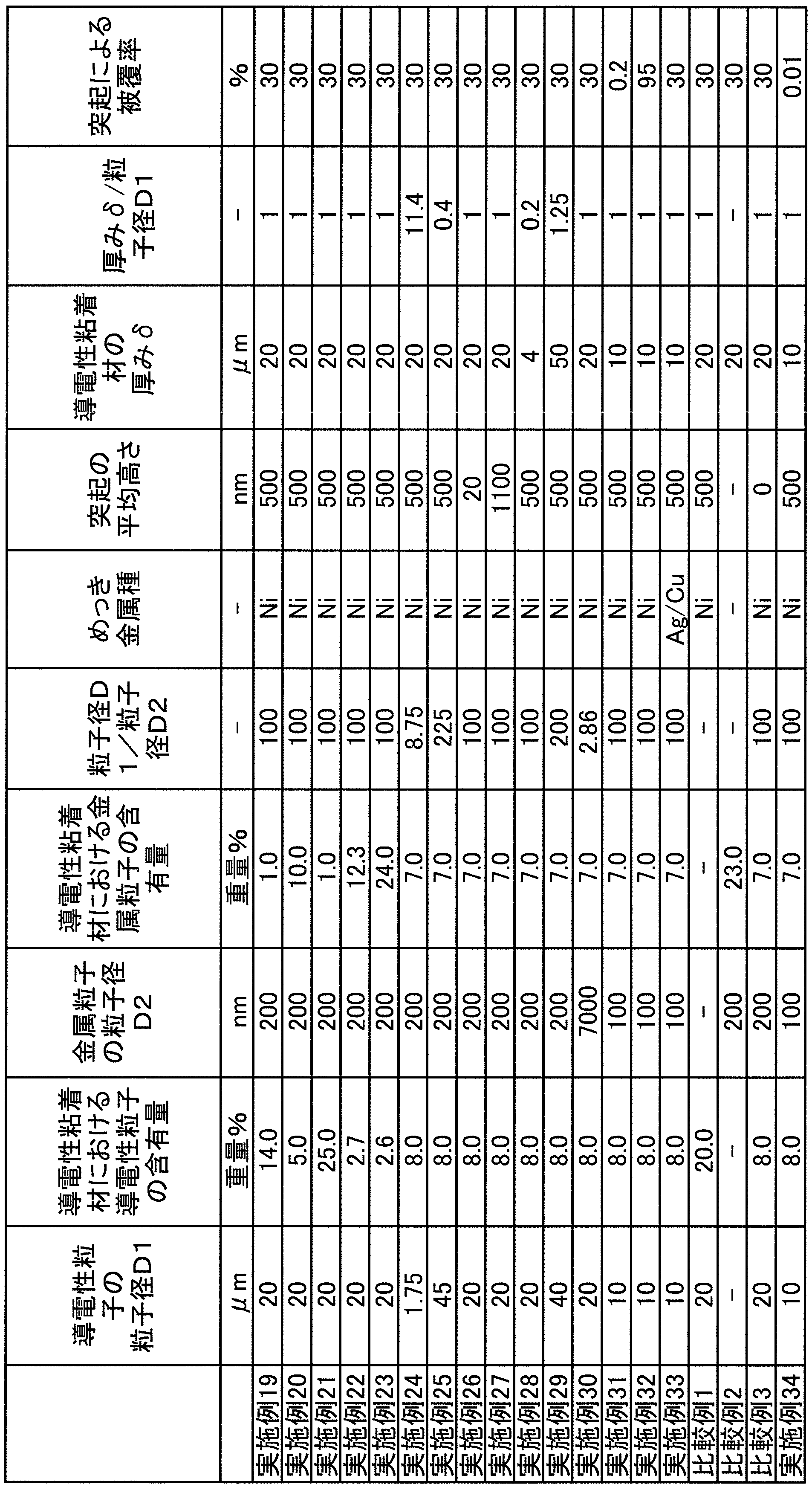
- Examples 19-23 As shown in Table 2, a conductive adhesive with a conductive substrate was obtained in the same manner as in Example 1 except that the content of conductive particles and the content of metal particles in the obtained conductive adhesive were changed. .
- Examples 24-25 As shown in Table 2, a conductive adhesive with a conductive substrate was obtained in the same manner as in Example 1 except that the particle diameter of the conductive particles was changed.
- Examples 26-27 As shown in Table 2, a conductive adhesive with a conductive substrate was obtained in the same manner as in Example 1 except that the average height of the protrusions of the conductive particles was changed.
- Example 28 As shown in Table 2, a conductive adhesive with a conductive substrate was obtained in the same manner as in Example 1 except that the thickness of the conductive adhesive was changed.
- Example 29 As shown in Table 2, a conductive adhesive with a conductive substrate was obtained in the same manner as in Example 1 except that the particle diameter of the conductive particles and the thickness of the conductive adhesive were changed.
- Example 30 As shown in Table 2, a conductive adhesive with a conductive substrate was obtained in the same manner as in Example 1 except that the particle diameter of the metal particles was changed.
- Examples 31-32 As shown in Table 2, a conductive adhesive with a conductive substrate was obtained in the same manner as in Example 4 except that the coverage by the protrusions of the conductive particles was changed.
- Example 33 As shown in Table 2, a conductive adhesive with a conductive substrate was prepared in the same manner as in Example 4 except that the plating metal type (layer configuration, outermost layer Ag / inner layer Cu) of the conductive part of the conductive particles was changed. Obtained.
- Example 1 As shown in Table 2, the conductivity with the conductive base material was the same as in Example 1 except that the content of the conductive particles in the conductive adhesive material was changed and the metal particles were not used in the conductive adhesive material. An adhesive was obtained.
- Example 2 As shown in Table 2, the conductivity with the conductive base material was the same as in Example 1 except that the content of the metal particles in the conductive adhesive material was changed and the conductive particles were not used in the conductive adhesive material. An adhesive was obtained.
- Example 3 As shown in Table 2, a conductive adhesive with a conductive substrate was obtained in the same manner as in Example 1 except that conductive particles having no protrusions (average height of protrusions of 0 nm) were used.
- Example 34 As shown in Table 2, a conductive adhesive with a conductive substrate was obtained in the same manner as in Example 4 except that the coverage by the protrusions of the conductive particles was changed.
- Adhesiveness A test piece (conductive adhesive material with a conductive base material) was attached to a stainless steel plate from the conductive adhesive material side, and the force required to peel it off from the test plate in the 180 ° direction was evaluated. The tensile speed was 30 mm / min, and the tape width was 25 mm. From the force required to peel off, the tackiness was determined according to the following criteria.
- connection resistance As shown in FIG. 6, the conductive adhesive 61 with a conductive base material is attached to the lower pure copper electrode 62 (25 ⁇ 25 mm) from the adhesive material side, and sandwiched between the upper pure copper electrode 63 and 2 MPa applied. In the pressed state, the connection resistance was measured using the four probe method. The plane area of the conductive adhesive with a conductive substrate was 10 ⁇ 10 mm. Connection resistance was determined according to the following criteria.
- Electromagnetic wave shielding property Using the KEC method (magnetic field) developed by KEC Kansai Electronics Industry Promotion Center, the electromagnetic wave shielding property of the conductive adhesive with a conductive substrate was evaluated. The shielding effect against 1 GHz high frequency was used as a comparison standard, and the electromagnetic shielding properties were evaluated from the obtained shielding effect value.
- Electromagnetic Shield Durability The conductive adhesive material with a conductive base material was subjected to a heat cycle test under the following heat cycle conditions, and then the shielding property was evaluated by the KEC method. Using the shielding effect against 1 GHz high frequency as a reference, the electromagnetic shielding durability was evaluated from the obtained shielding effect value.
- Heat cycle conditions low temperature side: ⁇ 10 ° C./30 min, high temperature side: 120 ° C./30 min, total 250 cycles.
Landscapes
- Chemical & Material Sciences (AREA)
- Organic Chemistry (AREA)
- Engineering & Computer Science (AREA)
- Microelectronics & Electronic Packaging (AREA)
- Inorganic Chemistry (AREA)
- Conductive Materials (AREA)
- Shielding Devices Or Components To Electric Or Magnetic Fields (AREA)
- Non-Insulated Conductors (AREA)
- Laminated Bodies (AREA)
- Adhesive Tapes (AREA)
- Adhesives Or Adhesive Processes (AREA)
Abstract
Description
本発明の導電性粘着材は、上述のように導電性基材に配置させることにより、導電性粘着シートや導電性粘着テープ等とすることができる。上記導電性基材としては、金属箔、金属メッシュ及び金属板等の金属基材が挙げられる。上記導電性基材の材料としては、銅及びアルミニウム等が挙げられる。上記金属箔としては、銅箔及びアルミニウム箔等が挙げられる。
電磁波シールド機能を効果的に高める観点から、上記導電性粘着材の厚みは、好ましくは5μm以上、より好ましくは10μm以上であり、好ましくは40μm以下、より好ましくは30μm以下、更に好ましくは20μm以下である。
上記金属粒子は、中心部及び表面部の双方が金属により形成されている金属粒子である。この金属粒子は、中心部において、金属粒子を除く基材粒子を有さない。中心部、表面部の金属種やその割合は同じであっても異なっていてもよい。
図2は、本発明の一実施形態に係る導電性基材付き導電性粘着材における導電性粘着材に用いた導電性粒子を示す断面図である。
上記基材粒子は、金属粒子を除く基材粒子である。上記基材粒子としては、樹脂粒子、金属粒子を除く無機粒子及び有機無機ハイブリッド粒子等が挙げられる。上記基材粒子は、樹脂粒子、金属粒子を除く無機粒子又は有機無機ハイブリッド粒子であることが好ましい。上記基材粒子は、コアと、該コアの表面上に配置されたシェルとを有していてもよく、コアシェル粒子であってもよい。上記コアが有機コアであってもよく、上記シェルが無機シェルであってもよい。
上記芯物質が上記導電部中に埋め込まれていることによって、上記導電部が外表面に、複数の突起を有するようにすることが容易である。
本発明の導電性粘着材は、粘着成分を有し、上述のように導電性基材に配置させることにより、導電性粘着シートや導電性粘着テープ等とすることができる。上記粘着成分としては、ゴム系粘着剤、アクリル系粘着剤、シリコーン系粘着剤、及びポリウレタン系粘着剤が挙げられる。上記粘着成分は1種のみが用いられてもよく、2種以上が併用されてもよい。
(1)導電性粘着材を形成するための導電性粘着材の溶液の調製
溶媒として酢酸エチルを用い、開始剤としてアゾビスイソブチロニトリル0.1重量部を用い、2-フェノキシエチルメタクリラート40重量部、メタクリル酸n-ブチル58重量部及びメタクリル酸2重量部を、溶液重合方法によって重合させ(60℃4時間、85℃1時間)、重量平均分子量が約40万のアクリル系ポリマーの溶液(固形分濃度:45重量%)を得た。このアクリル系ポリマー溶液の固形分100重量部に対して、粘着付与樹脂として重合ロジンペンタエリスリトールエステル(ハリマ化成グループ社製「ハリエスターS」)40重量部を配合し、アクリル系樹脂組成物溶液を作製した。
厚みが12μmである銅箔を用意した。この銅箔上に、上記導電性粘着材の溶液を用いて、バーコーターを用いて、厚みが20μmなるように導電性粘着材(粘着層)を形成して、さらに50℃で一日間エージングして、導電性基材付き導電性粘着材を得た。得られた導電性粘着材において、導電性粒子の含有量は8重量%、金属粒子の含有量は7重量%であった。
表1のように、導電性粒子の粒子径を変更したこと以外は、実施例1と同様に導電性基材付き導電性粘着材を得た。
表1のように、導電性粒子の粒子径及び金属粒子の粒子径を変更したこと以外は、実施例1と同様に導電性基材付き導電性粘着材を得た。
表1のように、金属粒子の粒子径を変更したこと以外は、実施例1と同様に導電性基材付き導電性粘着材を得た。
表1のように、金属粒子の粒子径及び導電性粘着材の厚みを変更したこと以外は、実施例1と同様に導電性基材付き導電性粘着材を得た。
表1のように、導電性粘着材の厚みを変更したこと以外は、実施例1と同様に導電性基材付き導電性粘着材を得た。
表1のように、金属粒子の粒子径及び導電性粘着材の厚みを変更したこと以外は、実施例1と同様に導電性基材付き導電性粘着材を得た。
表1のように、導電性粒子の突起の平均高さを変更したこと以外は、実施例1と同様に導電性基材付き導電性粘着材を得た。
表1のように、導電性粒子の導電部のめっき金属種を変更したこと以外は、実施例1と同様に導電性基材付き導電性粘着材を得た。
表2のように、得られる導電性粘着材における導電性粒子の含有量及び金属粒子の含有量を変更したこと以外は、実施例1と同様に導電性基材付き導電性粘着材を得た。
表2のように、導電性粒子の粒子径を変更したこと以外は、実施例1と同様に導電性基材付き導電性粘着材を得た。
表2のように、導電性粒子の突起の平均高さを変更したこと以外は、実施例1と同様に導電性基材付き導電性粘着材を得た。
表2のように、導電性粘着材の厚みを変更したこと以外は、実施例1と同様に導電性基材付き導電性粘着材を得た。
表2のように、導電性粒子の粒子径及び導電性粘着材の厚みを変更したこと以外は、実施例1と同様に導電性基材付き導電性粘着材を得た。
表2のように、金属粒子の粒子径を変更したこと以外は、実施例1と同様に導電性基材付き導電性粘着材を得た。
表2のように、導電性粒子の突起による被覆率を変更したこと以外は、実施例4と同様に導電性基材付き導電性粘着材を得た。
表2のように、導電性粒子の導電部のめっき金属種(層構成、最外層Ag/内層Cu)を変更したこと以外は、実施例4と同様に導電性基材付き導電性粘着材を得た。
表2のように、導電性粘着材における導電性粒子の含有量を変更し、かつ導電性粘着材に金属粒子を用いなかったこと以外は、実施例1と同様に導電性基材付き導電性粘着材を得た。
表2のように、導電性粘着材における金属粒子の含有量を変更し、かつ導電性粘着材に導電性粒子を用いなかったこと以外は、実施例1と同様に導電性基材付き導電性粘着材を得た。
表2のように、突起を有さない導電性粒子(突起の平均高さ0nm)を用いたこと以外は、実施例1と同様に導電性基材付き導電性粘着材を得た。
表2のように、導電性粒子の突起による被覆率を変更したこと以外は、実施例4と同様に導電性基材付き導電性粘着材を得た。
(1)粘着性
試験片(導電性基材付き導電性粘着材)をステンレス板に導電性粘着材側から貼りつけ、試験板から180°方向に引き剥がすのに要する力を評価した。引張速度は30mm/min、テープ幅は25mmとした。引き剥がすのに要する力から、粘着性を以下の基準で判定した。
○○○:15N/mm2以上
○○:10N/mm2以上、15N/mm2未満
○:4N/mm2以上、10N/mm2未満
△:1N/mm2以上、4N/mm2未満
×:1N/mm2未満
図6のように、導電性基材付き導電性粘着材61を粘着材側から、下部純銅電極62(25×25mm)に貼り付け、上部純銅電極63で挟んで、2MPa加圧した状態で、四端子法を用いて接続抵抗を測定した。導電性基材付き導電性粘着材の平面積を10×10mmとした。接続抵抗を以下の基準で判定した。
○○○:2Ω未満
○○:2Ω以上、5Ω未満
○:5Ω以上、10Ω未満
△:10Ω以上、30Ω未満
×:30Ω以上
KEC関西電子工業振興センター開発のKEC法(磁界)を用いて、導電性基材付き導電性粘着材の電磁波シールド性を評価した。1GHz高周波に対するシールド効果を比較基準とし、得られたシールド効果の値から、電磁波シールド性を評価した。
○○○:90dB以上
○○:75dB以上、90dB未満
○:60dB以上、75dB未満
△:40dB以上、60dB未満
×:40dB未満
導電性基材付き導電性粘着材について、以下のヒートサイクル条件でヒートサイクル試験を行った後、KEC法にてシールド性を評価した。1GHz高周波に対するシールド効果を比較基準とし、得られたシールド効果の値から、電磁波シールド耐久性を評価した。
○○○:80dB以上
○○:65dB以上、80dB未満
○:50dB以上、65dB未満
△:40dB以上、50dB未満
×:40dB未満


2…基材粒子
3,3A,3B,3C…導電部
3a,3Aa,3Ba,3Ca…突起
3BA,3CA…第1の導電部
3CAa…突起
3BB,3CB…第2の導電部
3BBa,3CBa…突起
4…芯物質
51…導電性基材付き導電性粘着材
52…導電性粘着材
53…導電性基材
56…金属粒子
57…粘着成分
Claims (12)
- 複数の金属粒子と、複数の導電性粒子と、粘着成分とを含み、
前記導電性粒子が、金属粒子を除く基材粒子と、前記基材粒子の表面上に配置された導電部とを備える導電性粒子であり、
前記導電性粒子が、前記導電部の外表面に複数の突起を有する、導電性粘着材。 - 導電性粘着材100重量%中、前記導電性粒子の含有量が1重量%以上、30重量%以下である、請求項1に記載の導電性粘着材。
- 前記導電性粒子の粒子径が3μm以上、40μm以下である、請求項1又は2に記載の導電性粘着材。
- 前記導電性粒子の体積抵抗率が0.001Ω・cm以下である、請求項1~3のいずれか1項に記載の導電性粘着材。
- 前記導電性粒子の粒子径の前記金属粒子の粒子径に対する比が0.7以上、5000以下である、請求項1~4のいずれか1項に記載の導電性粘着材。
- 前記突起の平均高さが30nm以上、1000nm以下である、請求項1~5のいずれか1項に記載の導電性粘着材。
- 前記導電部の外表面の全表面積100%中、前記突起がある部分の表面積が0.1%以上である、請求項1~6のいずれか1項に記載の導電性粘着材。
- 前記導電性粒子は、前記導電部の外表面を隆起させている複数の芯物質を備える、請求項1~7のいずれか1項に記載の導電性粘着材。
- 前記芯物質の材料のモース硬度が5以上である、請求項8に記載の導電性粘着材。
- 厚みが5μm以上、40μm以下である、請求項1~9のいずれか1項に記載の導電性粘着材。
- 請求項1~10のいずれか1項に記載の導電性粘着材と、
導電性基材とを有し、
前記導電性粘着材が、前記導電性基材の表面上に配置されている、導電性基材付き導電性粘着材。 - 前記導電性基材が銅箔である、請求項11に記載の導電性基材付き導電性粘着材。
Priority Applications (3)
| Application Number | Priority Date | Filing Date | Title |
|---|---|---|---|
| KR1020177015100A KR102529562B1 (ko) | 2015-05-20 | 2016-05-17 | 도전성 점착재 및 도전성 기재 부착 도전성 점착재 |
| CN201680010125.XA CN107250308B (zh) | 2015-05-20 | 2016-05-17 | 导电性粘合材料及带导电性基材的导电性粘合材料 |
| JP2016533665A JP6114883B1 (ja) | 2015-05-20 | 2016-05-17 | 導電性粘着材及び導電性基材付き導電性粘着材 |
Applications Claiming Priority (2)
| Application Number | Priority Date | Filing Date | Title |
|---|---|---|---|
| JP2015103078 | 2015-05-20 | ||
| JP2015-103078 | 2015-05-20 |
Publications (1)
| Publication Number | Publication Date |
|---|---|
| WO2016186099A1 true WO2016186099A1 (ja) | 2016-11-24 |
Family
ID=57320110
Family Applications (1)
| Application Number | Title | Priority Date | Filing Date |
|---|---|---|---|
| PCT/JP2016/064559 Ceased WO2016186099A1 (ja) | 2015-05-20 | 2016-05-17 | 導電性粘着材及び導電性基材付き導電性粘着材 |
Country Status (5)
| Country | Link |
|---|---|
| JP (1) | JP6114883B1 (ja) |
| KR (1) | KR102529562B1 (ja) |
| CN (1) | CN107250308B (ja) |
| TW (1) | TWI677558B (ja) |
| WO (1) | WO2016186099A1 (ja) |
Cited By (4)
| Publication number | Priority date | Publication date | Assignee | Title |
|---|---|---|---|---|
| WO2017104665A1 (ja) * | 2015-12-15 | 2017-06-22 | 積水化学工業株式会社 | 導電性粘着テープ |
| JP2019026821A (ja) * | 2017-08-03 | 2019-02-21 | トラス カンパニー リミテッドTruss Co.,Ltd | 導電性粘着テープ |
| WO2019077909A1 (ja) * | 2017-10-16 | 2019-04-25 | タツタ電線株式会社 | 導電性接着剤 |
| JP2021019012A (ja) * | 2019-07-17 | 2021-02-15 | 信越ポリマー株式会社 | 電磁波シールドフィルム、回路基板、及び回路基板の製造方法 |
Families Citing this family (2)
| Publication number | Priority date | Publication date | Assignee | Title |
|---|---|---|---|---|
| EP4075452A4 (en) * | 2019-12-10 | 2022-11-23 | Asahi Kasei Kabushiki Kaisha | CONDUCTIVE FILM AND WRAPPED BODY THEREOF |
| JP7528433B2 (ja) * | 2019-12-11 | 2024-08-06 | Dic株式会社 | 導電性粘着シート |
Citations (6)
| Publication number | Priority date | Publication date | Assignee | Title |
|---|---|---|---|---|
| JPS63301408A (ja) * | 1987-06-02 | 1988-12-08 | Hitachi Chem Co Ltd | 導電性粒子 |
| JP2005109160A (ja) * | 2003-09-30 | 2005-04-21 | Tokai Rubber Ind Ltd | 電磁波シールドテープおよびそれを用いたシールドフラットケーブル |
| JP2010034045A (ja) * | 2008-07-01 | 2010-02-12 | Hitachi Chem Co Ltd | 回路接続材料及び回路接続構造体 |
| JP2013058764A (ja) * | 2007-10-05 | 2013-03-28 | Hitachi Chemical Co Ltd | 接着剤組成物及びこれを用いた回路接続材料、並びに、回路部材の接続方法及び回路接続体 |
| JP2015010111A (ja) * | 2013-06-26 | 2015-01-19 | 日東電工株式会社 | 導電性粘着テープ |
| JP2015127392A (ja) * | 2013-11-27 | 2015-07-09 | 日東電工株式会社 | 導電性粘着テープ、電子部材及び粘着剤 |
Family Cites Families (10)
| Publication number | Priority date | Publication date | Assignee | Title |
|---|---|---|---|---|
| JP3296306B2 (ja) * | 1997-10-28 | 2002-06-24 | ソニーケミカル株式会社 | 異方導電性接着剤および接着用膜 |
| JP3741841B2 (ja) * | 1997-10-30 | 2006-02-01 | 信越ポリマー株式会社 | 異方導電性接着剤 |
| JP5375374B2 (ja) * | 2009-07-02 | 2013-12-25 | 日立化成株式会社 | 回路接続材料及び回路接続構造体 |
| JP5940760B2 (ja) * | 2010-05-19 | 2016-06-29 | 積水化学工業株式会社 | 導電性粒子、異方性導電材料及び接続構造体 |
| CN103124999B (zh) * | 2010-09-30 | 2015-06-10 | 积水化学工业株式会社 | 导电性粒子、各向异性导电材料及连接结构体 |
| JP5184612B2 (ja) * | 2010-11-22 | 2013-04-17 | 日本化学工業株式会社 | 導電性粉体、それを含む導電性材料及びその製造方法 |
| JP6009933B2 (ja) * | 2011-12-22 | 2016-10-19 | 積水化学工業株式会社 | 導電性粒子、導電材料及び接続構造体 |
| JP2013182823A (ja) * | 2012-03-02 | 2013-09-12 | Dexerials Corp | 接続体の製造方法、及び異方性導電接着剤 |
| WO2013132831A1 (ja) | 2012-03-06 | 2013-09-12 | 東洋インキScホールディングス株式会社 | 導電性微粒子およびその製造方法、導電性樹脂組成物、導電性シート、並びに電磁波シールドシート |
| JP5530571B1 (ja) * | 2012-11-28 | 2014-06-25 | 積水化学工業株式会社 | 絶縁性粒子付き導電性粒子、導電材料及び接続構造体 |
-
2016
- 2016-05-17 JP JP2016533665A patent/JP6114883B1/ja active Active
- 2016-05-17 CN CN201680010125.XA patent/CN107250308B/zh active Active
- 2016-05-17 KR KR1020177015100A patent/KR102529562B1/ko active Active
- 2016-05-17 WO PCT/JP2016/064559 patent/WO2016186099A1/ja not_active Ceased
- 2016-05-20 TW TW105115838A patent/TWI677558B/zh active
Patent Citations (6)
| Publication number | Priority date | Publication date | Assignee | Title |
|---|---|---|---|---|
| JPS63301408A (ja) * | 1987-06-02 | 1988-12-08 | Hitachi Chem Co Ltd | 導電性粒子 |
| JP2005109160A (ja) * | 2003-09-30 | 2005-04-21 | Tokai Rubber Ind Ltd | 電磁波シールドテープおよびそれを用いたシールドフラットケーブル |
| JP2013058764A (ja) * | 2007-10-05 | 2013-03-28 | Hitachi Chemical Co Ltd | 接着剤組成物及びこれを用いた回路接続材料、並びに、回路部材の接続方法及び回路接続体 |
| JP2010034045A (ja) * | 2008-07-01 | 2010-02-12 | Hitachi Chem Co Ltd | 回路接続材料及び回路接続構造体 |
| JP2015010111A (ja) * | 2013-06-26 | 2015-01-19 | 日東電工株式会社 | 導電性粘着テープ |
| JP2015127392A (ja) * | 2013-11-27 | 2015-07-09 | 日東電工株式会社 | 導電性粘着テープ、電子部材及び粘着剤 |
Cited By (8)
| Publication number | Priority date | Publication date | Assignee | Title |
|---|---|---|---|---|
| WO2017104665A1 (ja) * | 2015-12-15 | 2017-06-22 | 積水化学工業株式会社 | 導電性粘着テープ |
| JP2019026821A (ja) * | 2017-08-03 | 2019-02-21 | トラス カンパニー リミテッドTruss Co.,Ltd | 導電性粘着テープ |
| CN109385225A (zh) * | 2017-08-03 | 2019-02-26 | 特乐司有限公司 | 利用可压缩变形的导电性粉末的导电性胶带及其制造方法 |
| WO2019077909A1 (ja) * | 2017-10-16 | 2019-04-25 | タツタ電線株式会社 | 導電性接着剤 |
| JP2019073622A (ja) * | 2017-10-16 | 2019-05-16 | タツタ電線株式会社 | 導電性接着剤 |
| KR20200071104A (ko) * | 2017-10-16 | 2020-06-18 | 타츠타 전선 주식회사 | 도전성 접착제 |
| KR102337623B1 (ko) | 2017-10-16 | 2021-12-09 | 타츠타 전선 주식회사 | 도전성 접착제 |
| JP2021019012A (ja) * | 2019-07-17 | 2021-02-15 | 信越ポリマー株式会社 | 電磁波シールドフィルム、回路基板、及び回路基板の製造方法 |
Also Published As
| Publication number | Publication date |
|---|---|
| CN107250308A (zh) | 2017-10-13 |
| JPWO2016186099A1 (ja) | 2017-06-15 |
| CN107250308B (zh) | 2019-10-25 |
| TW201708469A (zh) | 2017-03-01 |
| TWI677558B (zh) | 2019-11-21 |
| KR102529562B1 (ko) | 2023-05-09 |
| KR20180006872A (ko) | 2018-01-19 |
| JP6114883B1 (ja) | 2017-04-12 |
Similar Documents
| Publication | Publication Date | Title |
|---|---|---|
| JP6114883B1 (ja) | 導電性粘着材及び導電性基材付き導電性粘着材 | |
| JP6470810B2 (ja) | 絶縁性粒子付き導電性粒子、導電材料及び接続構造体 | |
| JP6009933B2 (ja) | 導電性粒子、導電材料及び接続構造体 | |
| JP6165626B2 (ja) | 導電性粒子、導電材料及び接続構造体 | |
| JP6004983B2 (ja) | 導電性粒子、導電材料及び接続構造体 | |
| JP6084868B2 (ja) | 導電性粒子、導電材料及び接続構造体 | |
| KR102095291B1 (ko) | 절연성 입자 부착 도전성 입자, 도전 재료 및 접속 구조체 | |
| JPWO2013108842A1 (ja) | 導電性粒子、導電材料及び接続構造体 | |
| JP7132274B2 (ja) | 導電性粒子、導電材料及び接続構造体 | |
| JP2014026971A (ja) | 導電性粒子、導電材料及び接続構造体 | |
| JP6478308B2 (ja) | 導電性粒子、導電材料及び接続構造体 | |
| KR102805388B1 (ko) | 도전성 입자, 도전 재료 및 접속 구조체 | |
| JP2018137225A (ja) | 導電性粒子、導電材料及び接続構造体 | |
| JP6747816B2 (ja) | 導電性粒子、導電材料及び接続構造体 | |
| WO2022260159A1 (ja) | 被覆粒子、被覆粒子の製造方法、樹脂組成物及び接続構造体 | |
| KR102793665B1 (ko) | 절연성 입자 구비 도전성 입자, 도전 재료 및 접속 구조체 | |
| JP7132112B2 (ja) | 導電フィルム及び接続構造体 | |
| JP2015056306A (ja) | 導電性粒子、導電材料及び接続構造体 | |
| JP6066734B2 (ja) | 導電性粒子、導電材料及び接続構造体 | |
| JP2025037114A (ja) | 導電性粒子、導電材料及び接続構造体 | |
| JP2014026970A (ja) | 導電性粒子、導電材料及び接続構造体 | |
| JP2020013787A (ja) | 導電材料及び接続構造体 | |
| KR20200140808A (ko) | 절연성 입자를 갖는 도전성 입자, 절연성 입자를 갖는 도전성 입자의 제조 방법, 도전 재료 및 접속 구조체 | |
| JP2015057769A (ja) | 導電性粒子、導電材料及び接続構造体 |
Legal Events
| Date | Code | Title | Description |
|---|---|---|---|
| ENP | Entry into the national phase |
Ref document number: 2016533665 Country of ref document: JP Kind code of ref document: A |
|
| 121 | Ep: the epo has been informed by wipo that ep was designated in this application |
Ref document number: 16796492 Country of ref document: EP Kind code of ref document: A1 |
|
| ENP | Entry into the national phase |
Ref document number: 20177015100 Country of ref document: KR Kind code of ref document: A |
|
| NENP | Non-entry into the national phase |
Ref country code: DE |
|
| 122 | Ep: pct application non-entry in european phase |
Ref document number: 16796492 Country of ref document: EP Kind code of ref document: A1 |